EP0122081B1 - Semiconductor memory device - Google Patents
Semiconductor memory device Download PDFInfo
- Publication number
- EP0122081B1 EP0122081B1 EP84302045A EP84302045A EP0122081B1 EP 0122081 B1 EP0122081 B1 EP 0122081B1 EP 84302045 A EP84302045 A EP 84302045A EP 84302045 A EP84302045 A EP 84302045A EP 0122081 B1 EP0122081 B1 EP 0122081B1
- Authority
- EP
- European Patent Office
- Prior art keywords
- data
- memory device
- data line
- lines
- address
- Prior art date
- Legal status (The legal status is an assumption and is not a legal conclusion. Google has not performed a legal analysis and makes no representation as to the accuracy of the status listed.)
- Expired
Links
Images


Classifications
-
- G—PHYSICS
- G06—COMPUTING OR CALCULATING; COUNTING
- G06T—IMAGE DATA PROCESSING OR GENERATION, IN GENERAL
- G06T1/00—General purpose image data processing
- G06T1/60—Memory management
-
- G—PHYSICS
- G11—INFORMATION STORAGE
- G11C—STATIC STORES
- G11C7/00—Arrangements for writing information into, or reading information out from, a digital store
- G11C7/10—Input/output [I/O] data interface arrangements, e.g. I/O data control circuits, I/O data buffers
-
- G—PHYSICS
- G11—INFORMATION STORAGE
- G11C—STATIC STORES
- G11C7/00—Arrangements for writing information into, or reading information out from, a digital store
- G11C7/10—Input/output [I/O] data interface arrangements, e.g. I/O data control circuits, I/O data buffers
- G11C7/1006—Data managing, e.g. manipulating data before writing or reading out, data bus switches or control circuits therefor
Definitions
- the present invention relates to a semiconductor memory device, and more particularly, to a semiconductor memory device used, for example, for storing graphic data.
- a graphic data memory is used for storing graphic data being processed.
- the graphic memory often stores graphic data in correspondence to the graph or picture displayed by a graphic display apparatus.
- data processing such as compressing, differentiating, smoothing, and so on.
- data processing it is necessary to read out and process the data not only of the designated memory cell but also of the memory cells in the periphery thereof. Therefore, it is desirable that, in such a graphic memory and the like, not only the designated memory cell but also the memory cells in the periphery thereof can be quickly accessed.
- the memory cells from which data can be read out in parallel are limited to those included within each cell group, and it is impossible to read out data simultaneously from memory cells belonging to different cell groups.
- GB-A-2 092 785 discloses a window-scanned memory, allowing parallel access to a set of memory cells in respective sub-memories which describe an array of sample points in an access window.
- the access window can be shifted to any selected region of the field of sample points by providing an address of one of the sample points in the array.
- the set of memory cells is accessed for data input and output using respective input and output multiplexors, requiring address calculations to be performed.
- a memory device comprising: a plurality of memory cells; a plurality of word lines; a plurality of data lines used for write-in of data to, and/or readout of data from, said memory cells, the memory cells being connected between the word lines and the data lines; a word decoder for selecting one of the word lines; a column decoder having a plurality of output ends corresponding to the respective data lines; a first data bus for transferring data of a target memory cell; a second data bus for transferring data of a memory cell arranged in a predetermined position with respect to the target memory cell; a data line selecting circuit for selectively connecting said data lines to said data buses in response to an address signal; characterised in that: the memory device is a semiconductor memory device; the data line selecting circuit has a plurality of first transfer gate transistors and a plurality of second transfer gate transistors; each of the data lines is connected through one of the first transfer gate transistors to the first data bus, and is connected through one of said second transfer
- the present invention uses the idea of making it possible to simultaneously access a memory cell connected to a word line and a data line and memory cells connected to the word line and one or more data lines which are disposed in locations having predetermined relationships with the location of the data line, by selecting the word line and the data line, in a semiconductor memory device used as a graphic data memory device and the like.
- An embodiment of the present invention can make it possible to simultaneously read out the data from a target memory cell and one or more memory cells disposed in the periphery thereof with a short access time, thereby reducing the time for graphic data processing and so on, and increasing the efficiency of the data processing.
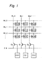
- Figure 1 illustrates an example of a conventional semiconductor memory device.
- the memory device shown in Fig. 1 is composed of word lines WL0, WL1, WL2, ...; data lines BL0, BL1, BL2, ...; memory cells MC00, MC01, MC02, ..., MC10, MC11, MC12, ..., and MC20, MC21, MC22, ...; a data bus DB; transistors Q0, Q1, Q2, ...; connected between the data lines BL0, BL1, BL2, ... and the data bus DB, respectively; and column decoders CD0, CD1, CD2, ... which supply a column selecting signal to the gates of the transistors Q0, Q1 Q2, ... respectively.
- each of the data lines BL0, BL1, BL2, ... and the data bus DB is shown by a single solid line, for simplicity. However, in practice, it should be noted that each of these data lines and the data bus is constituted of a pair of signal lines transmitting logic signals having opposite polarity.
- a selecting signal having, for example, a high potential level is applied to the word line WL1 from a row decoder (not shown in the drawing).
- the memory cells MC01, MC11, MC21, --- connected to the word line WL1 are selected, and data read out from these memory cells is output to the corresponding data lines BL0, BL1, BL2, ---, respectively.
- the transistor Q1 is turned on by the column decoder CD, and the data line BL1 and the data bus DB are connected. Therefore, the readout data from the memory cells MC11 is output through the data line BL1 and the data bus DB, so that a readout operation is performed.
- Figure 2 illustrates another example of a conventional semiconductor memory device.
- the memory device shown in Fig. 2 is constituted of memory cells MC00, MC01, MC02 ---, MC10, MC11, --- connected between word lines WL0, WL1, WL2, --- and data lines BL0, BL1, BL2, BL3, ---; transistors Q0 , Q1 , Q2 , --- connected between the data lines BL0, BL1, BL2, BL3, --- and data buses DB0, DB1, DB2, DB3; a column decoder CD0 which commonly controls the transistors Q0 through Q3 among these transistors and other column decoders.
- the memory device shown in Fig. 2 it is possible to simultaneously read out the data from the four memory cells MC01, MC11, MC21, MC31 among the memory cells connected to a word line, e.g., WL1 to the data buses DB0, DB1, DB2, DB3 , by selecting the word line WL1 and applying a column selecting signal to the transistors Q0 , Q1 , Q2 , Q3 from the column decoderCD0. That is, in the memory device shown in Fig. 2, it is possible to effect a parallel readout operation in which four bits of data are read out at the same time by designating one address.
- a word line e.g., WL1 to the data buses DB0, DB1, DB2, DB3
- the memory cells from which data can be read out in parallel are limited to those connected to the data lines of a predetermined data line group. It is impossible to read out data simultaneously from memory cells connected to the different sets (groups) of the data lines. Therefore, if the target memory cell is such a cell, for example MC31, that is connected to a data line disposed at either end of a data line group, it is impossible to read out the data from memory cells on both sides of the target memory cell at the same time, and it is necessary to separately access the memory cell(s) adjacently disposed on either side of the target memory cell.
- Figure 3 partially illustrates a structure of a semiconductor memory device which is an embodiment of the present invention.
- the memory device shown in Fig. 3 comprises word lines WL0, WL1, WL2, ---; data lines BL0, BL1, BL2, ---; memory cells MC00, MC01, MC02, ---, MC10, MC11,MC12, ---; three data buses DB-1, DB0, DB+1; column decoders CD0, CD1, CD2, ---; transistors used for transfer gates Q00 , Q01 , Q02 , Q10 , Q11 , Q12 , ---; and so on.
- the transistors Q00 , Q01 Q02 are connected between the data line BL0 and the data buses DB-1, DB0, DB+1, respectively, the transistors Q10 , Q11 , Q12 are connected between the data line BL1 and the data buses DB-1, DB0, DB+1 respectively, and each of the other transistors is connected between the corresponding data line and the corresponding data bus in a similar manner.
- These transistors constitute a data line selecting circuit.
- the output of each column decoder is connected to the gate of the transistor connected between a data line and the data bus DB0, and to the gates of the transistors connected between the data lines disposed on each side of the data line and the data buses DB-1 and DB+1, respectively.
- the output of the column decoder CD1 is commonly connected to the gate of the transistor Q11 connected between the data line BL1 and the data bus DB0, to the gate of the transistor Q00 connected between the data line BL0 and the data bus DB-1, and to the gate of the transistor Q22 connected between the data line BL2 and the data bus DB+1.
- a data line is the line connecting the memory cells and the transfer gates disposed in one column.
- the data line BL0 connects the memory cells MC00, MC01, MC02, --- and the transistors Q00 , Q01 , Q02.
- the memory cell MC11 is the target memory cell
- a column selecting signal is output from the column decoder CD1 and, thereby, the transistors Q00 and Q22 as well as the transistor Q11 are turned on. Therefore, the data read out from the memory cell MC11 is output through the data line BL1, the transistor Q11 , and the data bus DB0 and, moreover, the data read out from the memory cells MC01 and MC21 disposed adjacently on both sides of the memory cell MC11 is output through the data lines BL0 and BL2, the transistors Q00 and Q22 , and the data buses DB-1 and DB+1, respectively.
- the target memory cell is MC11 and when it is necessary to read out the data from nine memory cells in the periphery of and including the memory cell MC11, i.e., MC00, MC01, MC02, MC10, MC11, MC12, MC20, MC21, and MC22, in order to perform graphic data processing, it is possible to read out the data by a three times access operation in which the word lines WL0, WL1 and WL2 are sequentially selected together with the selection of the column decoder CD1.
- data is read out from the target memory cell and the memory cells adjacently disposed on both sides thereof at the same time.
- the memory cells from which data is read out simultaneously with the target memory cell are not limited to the memory cells adjacent the target memory cell but can be memory cells whose locations have any predetermined relationship to the target memory cell, or can be memory cells whose addresses have a predetermined relationship thereto.
- data write-in can be effected by supplying data just to one data bus, for example, DB0, in the data write-in time, in a manner similar to the conventional device. It is also possible to write-in the data in parallel to the target memory cell and the peripheral memory cells simultaneously by supplying data to the data buses DB0, DB-1, and DB+1.
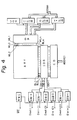
- Figure 4 illustrates a semiconductor memory device as another embodiment of the present invention.
- the semiconductor memory device shown in Fig. 4 comprises a memory cell array ARY having a plurality of memory cells arranged in a matrix, an input/output gate IOG connected to the memory cell array ARY through data lines BL0, BL1, ---, BLn, a column decoder CD, and a word decoder WD connected to the memory cell array ARY through word lines WL0, WL1, ---, WLn.
- the input/output gate comprises transfer gate circuits such as the transfer gate transistors of the memory device shown in Fig.
- the device shown in Fig. 4 further comprises output buffers OB-1, OB0, and OB+1 connected to the input/output gate LOG via data buses DB-1, DB0, and DB+1, respectively; data input buffers DIB-1, DIB0, and DIB+1 which are also connected to the input/output gate IOG via data buses DB-1, DB0, and DB+1, respectively; a read/write control circuit RWC controlling these buffers; address buffers BUF-1, BUF, and BUF+1 connected to the word decoder CD; and an address control circuit ADC controlling these address buffers.
- the address buffers BUF-1 and BUF+1 comprise, for example a decrement circuit and an increment circuit for generating decremented and incremented address signals from an input word address signal ADD(W).
- the gate circuits of the input/output gate IOG are arranged for memory access of cells in a particular predetermined relationship. If a programmable logic array (PLA) is used to form the input/output gate IOG, the predetermined relationship may be altered when, for example, readout of nine memory cells is required, a word address signal ADD(W) is applied to the address buffers BUF-1, BUF0, and BUF+1 and a column address signal ADD(C) is applied to the column decoder CD.
- PDA programmable logic array
- the address control circuit ADC applies a control signal to the address buffer BUF0, and the address buffer BUF0 supplies the buffered word address signal corresponding to the input word decoder WD.
- the word decoder selects a word line, for example,
- the input/output gate IOG transfers the data on the three data lines designated by the column address signal ADD(C) to the data buses DB-1, DB0, and DB+1 under the control of the column decoder CD.
- the data on the data buses DB-1, DB0, and DB+1 is output via the output buffers OB-1, OB0, and OB+1, respectively, which are activated by the read/write control circuit RWC in accordance with a write-enable signal WE having, for example, a high potential level.
- the address control circuit ADC supplies the control signal to the address buffer BUF-1.
- the address buffer BUF-1 generates a decremented address signal designating, for example, a word line WL1, from the input word address ADD(W) and supplies the decremented address signal to the word decoder WD. Therefore, the word line, for example, WL1, is selected and the data is read out from three memory cells which are connected to the word line WL1 and which are selected by the column address signal ADD(C), in the same manner as previously mentioned.
- the address control circuit ADC then supplies the control signal to the address buffer BUF+1.
- the address buffer BUF+1 generates an incremented address signal designating, for example, a word line WL3, from the input word address ADD(W) and supplies the incremented address signal to the word decoder WD. Therefore, the data is read out from three memory cells connected to the word line WL3 and selected by the column address signal ADD(C) in the same manner as previously mentioned.
- the semiconductor memory device shown in Fig. 4 it is possible to read out the data not only from the target memory cell but also the eight memory cells in the periphery thereof in the same operation, by designating only the target memory cell by the word address ADD(W) and the column address ADD(C).
- the write-in operation may be performed similarly by supplying input data Din(-1), Din(0), and Din (+1) to the data input buffers DIB-1, DIB0, and DIB+1 and by supplying the word address ADD(W) and the column address ADD(C).
- the write enable signal WE is rendered, for example, low, so that the read/write control circuit RWC enables the data input buffers DIB-1, DIB0, and DIB+1.
- the present invention it is possible to simultaneously access not only a target memory cell but also memory cells whose locations have a predetermined relationship to the target memory cell, such as the memory cells adjacently disposed on both sides of the target memory cell.
Landscapes
- Physics & Mathematics (AREA)
- General Physics & Mathematics (AREA)
- Engineering & Computer Science (AREA)
- Theoretical Computer Science (AREA)
- Dram (AREA)
- Static Random-Access Memory (AREA)
- Image Input (AREA)
- Controls And Circuits For Display Device (AREA)
Applications Claiming Priority (2)
| Application Number | Priority Date | Filing Date | Title |
|---|---|---|---|
| JP53586/83 | 1983-03-31 | ||
| JP58053586A JPS59180324A (ja) | 1983-03-31 | 1983-03-31 | 半導体記憶装置 |
Publications (3)
| Publication Number | Publication Date |
|---|---|
| EP0122081A2 EP0122081A2 (en) | 1984-10-17 |
| EP0122081A3 EP0122081A3 (en) | 1988-03-09 |
| EP0122081B1 true EP0122081B1 (en) | 1991-05-29 |
Family
ID=12946955
Family Applications (1)
| Application Number | Title | Priority Date | Filing Date |
|---|---|---|---|
| EP84302045A Expired EP0122081B1 (en) | 1983-03-31 | 1984-03-27 | Semiconductor memory device |
Country Status (4)
| Country | Link |
|---|---|
| US (1) | US4597063A (enExample) |
| EP (1) | EP0122081B1 (enExample) |
| JP (1) | JPS59180324A (enExample) |
| DE (1) | DE3484630D1 (enExample) |
Families Citing this family (16)
| Publication number | Priority date | Publication date | Assignee | Title |
|---|---|---|---|---|
| US4742474A (en) * | 1985-04-05 | 1988-05-03 | Tektronix, Inc. | Variable access frame buffer memory |
| JPH0783062B2 (ja) * | 1985-06-18 | 1995-09-06 | 株式会社東芝 | マスタ−スライス型半導体装置 |
| JPS62131289A (ja) * | 1985-12-03 | 1987-06-13 | 日本電気株式会社 | 図形表示装置用の記憶回路 |
| DE3774369D1 (de) * | 1986-08-22 | 1991-12-12 | Fujitsu Ltd | Halbleiter-speicheranordnung. |
| JPS6381688A (ja) * | 1986-09-26 | 1988-04-12 | Hitachi Ltd | 半導体記憶装置 |
| US4811297A (en) * | 1986-12-16 | 1989-03-07 | Fujitsu Limited | Boundary-free semiconductor memory device |
| JP2603252B2 (ja) * | 1987-04-30 | 1997-04-23 | キヤノン株式会社 | 撮像装置 |
| JPS63308785A (ja) * | 1987-06-10 | 1988-12-16 | Fujitsu Ltd | 半導体記憶装置 |
| JPH01121715A (ja) * | 1987-11-05 | 1989-05-15 | Kokudo Joho Kaihatsu Kk | 地籍情報管理装置 |
| JPH01169063U (enExample) * | 1988-05-20 | 1989-11-29 | ||
| JP2783579B2 (ja) * | 1989-03-01 | 1998-08-06 | 株式会社東芝 | 半導体装置 |
| JPH03241598A (ja) * | 1990-02-19 | 1991-10-28 | Fujitsu Ltd | シグネチャー回路 |
| JPH0831276B2 (ja) * | 1990-06-15 | 1996-03-27 | 松下電器産業株式会社 | 半導体メモリ |
| JPH0548224A (ja) * | 1991-08-16 | 1993-02-26 | Matsushita Electric Ind Co Ltd | プリント基板 |
| JPH0682710U (ja) * | 1993-05-01 | 1994-11-25 | 博美 田村 | ハウス栽培用照明具 |
| US6711664B1 (en) * | 2000-09-13 | 2004-03-23 | Sun Microsystems, Inc. | Method and system for decoding a row address to assert multiple adjacent rows in a memory structure |
Family Cites Families (4)
| Publication number | Priority date | Publication date | Assignee | Title |
|---|---|---|---|---|
| US4045783A (en) * | 1976-04-12 | 1977-08-30 | Standard Microsystems Corporation | Mos one transistor cell ram having divided and balanced bit lines, coupled by regenerative flip-flop sense amplifiers, and balanced access circuitry |
| US4104735A (en) * | 1976-09-15 | 1978-08-01 | Siemens Aktiengesellschaft | Arrangement for addressing a MOS store |
| US4460958A (en) * | 1981-01-26 | 1984-07-17 | Rca Corporation | Window-scanned memory |
| JPS581872A (ja) * | 1981-06-25 | 1983-01-07 | Fujitsu Ltd | メモリアクセス方式 |
-
1983
- 1983-03-31 JP JP58053586A patent/JPS59180324A/ja active Granted
-
1984
- 1984-03-27 DE DE8484302045T patent/DE3484630D1/de not_active Expired - Lifetime
- 1984-03-27 EP EP84302045A patent/EP0122081B1/en not_active Expired
- 1984-03-29 US US06/594,630 patent/US4597063A/en not_active Expired - Lifetime
Also Published As
| Publication number | Publication date |
|---|---|
| US4597063A (en) | 1986-06-24 |
| EP0122081A2 (en) | 1984-10-17 |
| EP0122081A3 (en) | 1988-03-09 |
| JPS6336068B2 (enExample) | 1988-07-19 |
| JPS59180324A (ja) | 1984-10-13 |
| DE3484630D1 (de) | 1991-07-04 |
Similar Documents
| Publication | Publication Date | Title |
|---|---|---|
| EP0122081B1 (en) | Semiconductor memory device | |
| US5471603A (en) | Modular high-capacity solid-state mass data storage device including controller/memory modules arranged in parallel channels | |
| US4811297A (en) | Boundary-free semiconductor memory device | |
| US5229971A (en) | Semiconductor memory device | |
| US4740923A (en) | Memory circuit and method of controlling the same | |
| EP0646925B1 (en) | Fully scalable memory apparatus | |
| US4578780A (en) | Dual port type semiconductor memory | |
| US5361339A (en) | Circuit for fast page mode addressing of a RAM with multiplexed row and column address lines | |
| US5703810A (en) | DRAM for texture mapping | |
| US5666312A (en) | Column redundancy scheme for a random access memory incorporating multiplexers and demultiplexers for replacing defective columns in any memory array | |
| US6377492B1 (en) | Memory architecture for read and write at the same time using a conventional cell | |
| JPH0338678B2 (enExample) | ||
| EP0420339A2 (en) | Multi-plane random access memory system | |
| US5537355A (en) | Scheme to test/repair multiple large RAM blocks | |
| US5418745A (en) | Semiconductor memory device for continuously accessing a memory cell array divided according to a column address | |
| JPH0785693A (ja) | 半導体記憶装置 | |
| JP3061824B2 (ja) | 半導体メモリ | |
| JPH0227759B2 (enExample) | ||
| JPS58103063A (ja) | マトリクス記憶装置 | |
| KR100280470B1 (ko) | 플래시메모리의 데이터 입출력장치 | |
| JPH01211395A (ja) | Icメモリ | |
| JPH04285796A (ja) | 半導体記憶装置 | |
| JPS62146480A (ja) | 半導体記憶装置 | |
| JPH0444356B2 (enExample) | ||
| JPH01112592A (ja) | 半導体記憶装置 |
Legal Events
| Date | Code | Title | Description |
|---|---|---|---|
| PUAI | Public reference made under article 153(3) epc to a published international application that has entered the european phase |
Free format text: ORIGINAL CODE: 0009012 |
|
| AK | Designated contracting states |
Designated state(s): DE FR GB |
|
| PUAL | Search report despatched |
Free format text: ORIGINAL CODE: 0009013 |
|
| RHK1 | Main classification (correction) |
Ipc: G11C 8/00 |
|
| AK | Designated contracting states |
Kind code of ref document: A3 Designated state(s): DE FR GB |
|
| 17P | Request for examination filed |
Effective date: 19880712 |
|
| 17Q | First examination report despatched |
Effective date: 19891110 |
|
| GRAA | (expected) grant |
Free format text: ORIGINAL CODE: 0009210 |
|
| AK | Designated contracting states |
Kind code of ref document: B1 Designated state(s): DE FR GB |
|
| REF | Corresponds to: |
Ref document number: 3484630 Country of ref document: DE Date of ref document: 19910704 |
|
| ET | Fr: translation filed | ||
| PLBE | No opposition filed within time limit |
Free format text: ORIGINAL CODE: 0009261 |
|
| STAA | Information on the status of an ep patent application or granted ep patent |
Free format text: STATUS: NO OPPOSITION FILED WITHIN TIME LIMIT |
|
| 26N | No opposition filed | ||
| PGFP | Annual fee paid to national office [announced via postgrant information from national office to epo] |
Ref country code: FR Payment date: 20010313 Year of fee payment: 18 |
|
| PGFP | Annual fee paid to national office [announced via postgrant information from national office to epo] |
Ref country code: DE Payment date: 20010319 Year of fee payment: 18 |
|
| PGFP | Annual fee paid to national office [announced via postgrant information from national office to epo] |
Ref country code: GB Payment date: 20010321 Year of fee payment: 18 |
|
| REG | Reference to a national code |
Ref country code: GB Ref legal event code: IF02 |
|
| PG25 | Lapsed in a contracting state [announced via postgrant information from national office to epo] |
Ref country code: GB Free format text: LAPSE BECAUSE OF NON-PAYMENT OF DUE FEES Effective date: 20020327 |
|
| PG25 | Lapsed in a contracting state [announced via postgrant information from national office to epo] |
Ref country code: DE Free format text: LAPSE BECAUSE OF NON-PAYMENT OF DUE FEES Effective date: 20021001 |
|
| GBPC | Gb: european patent ceased through non-payment of renewal fee |
Effective date: 20020327 |
|
| PG25 | Lapsed in a contracting state [announced via postgrant information from national office to epo] |
Ref country code: FR Free format text: LAPSE BECAUSE OF NON-PAYMENT OF DUE FEES Effective date: 20021129 |
|
| REG | Reference to a national code |
Ref country code: FR Ref legal event code: ST |