EP0112672B1 - System for processing machine check interruption - Google Patents
System for processing machine check interruption Download PDFInfo
- Publication number
- EP0112672B1 EP0112672B1 EP83307470A EP83307470A EP0112672B1 EP 0112672 B1 EP0112672 B1 EP 0112672B1 EP 83307470 A EP83307470 A EP 83307470A EP 83307470 A EP83307470 A EP 83307470A EP 0112672 B1 EP0112672 B1 EP 0112672B1
- Authority
- EP
- European Patent Office
- Prior art keywords
- machine check
- interruption
- signal
- data processor
- condition
- Prior art date
- Legal status (The legal status is an assumption and is not a legal conclusion. Google has not performed a legal analysis and makes no representation as to the accuracy of the status listed.)
- Expired
Links
Images
Classifications
-
- G—PHYSICS
- G06—COMPUTING OR CALCULATING; COUNTING
- G06F—ELECTRIC DIGITAL DATA PROCESSING
- G06F11/00—Error detection; Error correction; Monitoring
-
- G—PHYSICS
- G06—COMPUTING OR CALCULATING; COUNTING
- G06F—ELECTRIC DIGITAL DATA PROCESSING
- G06F11/00—Error detection; Error correction; Monitoring
- G06F11/07—Responding to the occurrence of a fault, e.g. fault tolerance
- G06F11/0703—Error or fault processing not based on redundancy, i.e. by taking additional measures to deal with the error or fault not making use of redundancy in operation, in hardware, or in data representation
- G06F11/0706—Error or fault processing not based on redundancy, i.e. by taking additional measures to deal with the error or fault not making use of redundancy in operation, in hardware, or in data representation the processing taking place on a specific hardware platform or in a specific software environment
- G06F11/0721—Error or fault processing not based on redundancy, i.e. by taking additional measures to deal with the error or fault not making use of redundancy in operation, in hardware, or in data representation the processing taking place on a specific hardware platform or in a specific software environment within a central processing unit [CPU]
-
- G—PHYSICS
- G06—COMPUTING OR CALCULATING; COUNTING
- G06F—ELECTRIC DIGITAL DATA PROCESSING
- G06F11/00—Error detection; Error correction; Monitoring
- G06F11/07—Responding to the occurrence of a fault, e.g. fault tolerance
- G06F11/0703—Error or fault processing not based on redundancy, i.e. by taking additional measures to deal with the error or fault not making use of redundancy in operation, in hardware, or in data representation
- G06F11/0751—Error or fault detection not based on redundancy
-
- G—PHYSICS
- G06—COMPUTING OR CALCULATING; COUNTING
- G06F—ELECTRIC DIGITAL DATA PROCESSING
- G06F11/00—Error detection; Error correction; Monitoring
- G06F11/07—Responding to the occurrence of a fault, e.g. fault tolerance
- G06F11/0703—Error or fault processing not based on redundancy, i.e. by taking additional measures to deal with the error or fault not making use of redundancy in operation, in hardware, or in data representation
- G06F11/0793—Remedial or corrective actions
Definitions
- the present invention relates to a system for processing machine check interruption and more particularly to a system for processing machine check interruption using a data processor in which a machine check interruption code is analyzed when a machine check interruption occurs; and if the contents of the machine check interruption code show a condition in which the operation of the hardware thereafter is not guaranteed, the data processor is rendered to be in a disabled-waiting condition.
- An exigent condition In an exigent condition, the central processing unit (CPU) is directly affected, and, therefore, it becomes impossible to proceed with the execution of the instructions and with the processing of the interruption.
- An exigent condition can be of two types: instruction processing damage (PD) and system damage (SD).
- PD instruction processing damage
- SD system damage
- An erroneous operation which cannot be discriminated as a specific kind is indicated as SD.
- the type SD includes SD occurring on a memory access route and SD occurring on a CPU route.
- jobs are generally executed under the management of the operating system.
- the interruption process for a machine check is carried out by software.
- the type SD also includes damage which makes the operation of hardware unreliable, for example, damage resulting in the erroneous operation of a memory control unit (MCU) which controls the memory access operation.
- MCU memory control unit
- the software sometimes does not judge such damage to be a system breakdown condition when the cause thereof is a certain kind but executes the processing so as to interrupt, i.e., to end abnormally, only the job at that time and to move on to the next job.
- GB-A-1 495 729 discloses a data processing system including analysing means, allowing an error in the system to be detected, error indicating means responsive to the analysing means and capable of supplying information about the error, and control means which in response to that information, identifies the mode in which the error has occurred and validates an error program for dealing with the error accordingly.
- the system can distinguish between an error merely arising in a currently-running process, and an error which involves the entire system.
- a system for processing machine check interruption using a data processor which outputs a machine check interruption signal by detecting the generation of a machine check condition and performs interruption processing on the basis of said machine check interruption signal
- said data processor comprising a specific code detector means which detects a specific interruption signal among the machine interruption signals, characterised in that said data processor further comprises a signal converting means for converting the machine check interruption signal into a modified code signal when the interruption signal generated by the machine check interruption is the above-mentioned specific interruption signal, and a control portion which assumes a disabled-waiting condition in response to said modified code signal, the operation of said data processor being stopped by rendering said control portion to be in a disabled-waiting condition when the above-mentioned specific interruption signal occurs.
- An embodiment of the present invention can thus provide, in order to solve the above-mentioned problems, a system for processing machine check interruption in which the machine check interruption code is converted into another data code in accordance with the portion which assumes a machine check condition and in accordance with the content of the machine check condition, thereby causing the software to assume a disabled-waiting condition and ensuring reliable data processing.
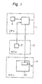
- the data processor of Figure 1 used in a system according to the present invention comprises a CPU 1, an MCU 2, and an MSU 3.
- the CPU 1 comprises, in addition to a general data processing portion (not shown), a signal generating portion 11, which generates a modified machine check interruption signal in response to the occurrence of a machine check interruption, and a fault detecting portion 4, which generates a machine check interruption signal when a fault is detected in the CPU 1.
- the MCU 2 also comprises a fault detecting portion 5 generating a machine check interruption signal when a fault is detected in the MCU 2.
- the MSU 3 comprises a control portion 20 which includes a register 19 for storing a machine check interruption code (hereinafter referred to as an MCIC register), and a machine check processing routine.
- MCIC register machine check interruption code
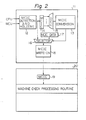
- FIG. 2 illustrates in detail the structure of the signal generating portion 11 and the control portion 20 used in the data processor of Figure 1.
- the signal generating portion 11 comprises a machine check detecting and holding portion 12, a control circuit 13 for converting the machine check interruption code (hereinafter referred to as an MCIC converting circuit), a code register 14, a decoder 15, a selector 16, a holding portion 17 for converted data of a machine check interruption code (hereinafter referred to as an MCIC conversion data portion), and a write-in portion 18 for a machine check interruption code (hereinafter referred to as an MCIC write-in portion).
- the control portion 20 in the MSU 3 includes, as was previously mentioned, the MCIC register 19 and the machine check processing routine.
- the machine check detecting and holding portion 12 detects the generation of a machine check interruption signal and stores the machine check interruption code.
- the machine check interruption code includes information on where the machine check interruption signal is generated and on the cause of the generation thereof. This information will be analyzed in a debugging process so as to determine what kind of abnormal phenomenon is generated in each portion of the data processor.
- the MCIC converting circuit 13 selects the input of the selector 16 so that either the output signal from the machine check detecting and holding portion 12 or the output signal from the MCIC conversion data portion 17 is output therefrom.
- the MCIC converting circuit 13 usually controls the selector 16 so that the machine check interruption signal sent from the machine check detecting and holding portion 12 is output from the selector 16.
- the MCIC converting circuit 13 receives the conversion command from the decoder 15, it controls the selector 16 so that the output signal sent from the MCIC conversion data portion 17 is output therefrom.
- the decoder 15 detects the condition that the machine check interruption signal sent from the machine check detecting and holding portion 12 indicates a state in which the erroneous device and the content data of the device show a condition in which operation of the hardware is unreliable, for example, a condition in which an address parity error is detected when data is written into a main storage unit. If the decoder 15 detects such a condition, it transmits a converting command output "1" to the MCIC converting circuit 13. The kinds of machine check interruption signals which lead to the generation of the converting command output "1" are previously determined.
- the MCIC conversion data portion 17 outputs, for example, all "0"s, and, when this all "0"s signal is output from the selector 16, the machine check processing routine of the control portion 20 cannot analyze where the machine check interruption signal is generated from or the cause of the generation thereof because of the all "0"s signal. Therefore, continuation of execution of the machine check interruption processing becomes impossible and the data processor assumes a disabled-waiting condition.
- the control portion 20 stores control programs necessary to control the various operations of the data processor and performs various control functions by using them.
- the control portion 20 also stores the machine check processing routine.
- the machine check detecting and holding portion 12 detects the machine check interruption signal and temporarily stores it.
- the machine check interruption signal is then sent from the machine check detecting and holding portion 12 to the code register 14 and the selector 16. If the machine check interruption code stored in the code register 14 shows an error, for example, in the CPU 1, by which the data processor will not be led to a system breakdown state, the decoder 15 outputs an "0" signal. Therefore, the MCIC converting circuit 13 controls the selector 16 so that it outputs the machine check interruption signal unchanged.
- This interruption signal is written into an output register (not shown) by the MCIC write-in portion 18 and is transmitted to the MCIC register 19 of the control portion 20.
- the place where the interruption signal is generated and the cause of the generated interruption are analyzed by the machine check processing routine on the basis of the machine check interruption signal, debugging thereby being executed.
- the decoder 15 judges that the machine check interruption signal is one of the signals showing a condition in which continued operation of the hardware would not be reliable, such as erroneous operation of the MCU, the decoder 15 outputs the conversion command output "1".
- the MCIC converting circuit 13 controls the selector 16 so that the selector outputs the all "0"s signal sent from the MCIC conversion data portion 17 in place of the machine check interruption signal transmitted from the machine check detecting and holding portion 12.
- the all "0"s signal is sent to the MCIC register 19 via the MCIC write-in portion 18, and the machine check processing routine of the control portion 20 analyzes the code stored in the MCIC register 19.
- the machine check interruption signal corresponds to a condition in which operation of the hardware from now on is reliable. If it is determined that the signal corresponds to a condition in which operation of the hardware is unreliable, the hardware processing is stopped. Therefore, data processing is reliably effected.
Landscapes
- Engineering & Computer Science (AREA)
- Theoretical Computer Science (AREA)
- Quality & Reliability (AREA)
- Physics & Mathematics (AREA)
- General Engineering & Computer Science (AREA)
- General Physics & Mathematics (AREA)
- Debugging And Monitoring (AREA)
- Hardware Redundancy (AREA)
- Computer And Data Communications (AREA)
Applications Claiming Priority (2)
| Application Number | Priority Date | Filing Date | Title |
|---|---|---|---|
| JP57228855A JPS59116858A (ja) | 1982-12-23 | 1982-12-23 | マシンチエツク割込み処理方式 |
| JP228855/82 | 1982-12-23 |
Publications (3)
| Publication Number | Publication Date |
|---|---|
| EP0112672A2 EP0112672A2 (en) | 1984-07-04 |
| EP0112672A3 EP0112672A3 (en) | 1987-05-13 |
| EP0112672B1 true EP0112672B1 (en) | 1989-08-09 |
Family
ID=16882929
Family Applications (1)
| Application Number | Title | Priority Date | Filing Date |
|---|---|---|---|
| EP83307470A Expired EP0112672B1 (en) | 1982-12-23 | 1983-12-08 | System for processing machine check interruption |
Country Status (9)
| Country | Link |
|---|---|
| US (1) | US4587654A (cg-RX-API-DMAC7.html) |
| EP (1) | EP0112672B1 (cg-RX-API-DMAC7.html) |
| JP (1) | JPS59116858A (cg-RX-API-DMAC7.html) |
| KR (1) | KR890001796B1 (cg-RX-API-DMAC7.html) |
| AU (1) | AU544915B2 (cg-RX-API-DMAC7.html) |
| BR (1) | BR8307085A (cg-RX-API-DMAC7.html) |
| CA (1) | CA1204876A (cg-RX-API-DMAC7.html) |
| DE (1) | DE3380369D1 (cg-RX-API-DMAC7.html) |
| ES (1) | ES8501902A1 (cg-RX-API-DMAC7.html) |
Families Citing this family (1)
| Publication number | Priority date | Publication date | Assignee | Title |
|---|---|---|---|---|
| US4916697A (en) * | 1988-06-24 | 1990-04-10 | International Business Machines Corporation | Apparatus for partitioned clock stopping in response to classified processor errors |
Family Cites Families (11)
| Publication number | Priority date | Publication date | Assignee | Title |
|---|---|---|---|---|
| US3229251A (en) * | 1962-03-26 | 1966-01-11 | Ibm | Computer error stop system |
| US3555517A (en) * | 1968-10-30 | 1971-01-12 | Ibm | Early error detection system for data processing machine |
| US3707714A (en) * | 1971-01-08 | 1972-12-26 | Honeywell Inc | Multiple error detector |
| JPS5519000B2 (cg-RX-API-DMAC7.html) * | 1973-07-11 | 1980-05-22 | ||
| JPS50117336A (cg-RX-API-DMAC7.html) * | 1973-11-30 | 1975-09-13 | ||
| IT1046598B (it) * | 1974-05-16 | 1980-07-31 | Honeywell Inf Systems | Interfaccia di connessione di apparecchiature periferiche a un calcolatore provvista di meccanismi di segnalazione e di distinzione tradiversi tipi di errore |
| JPS51146143A (en) * | 1975-06-11 | 1976-12-15 | Hitachi Ltd | Wedging process mode when logic device generates error action |
| US4044337A (en) * | 1975-12-23 | 1977-08-23 | International Business Machines Corporation | Instruction retry mechanism for a data processing system |
| JPS6032217B2 (ja) * | 1979-04-02 | 1985-07-26 | 日産自動車株式会社 | 制御用コンピュ−タのフェィルセ−フ装置 |
| DE3036926C2 (de) * | 1980-09-30 | 1984-07-26 | Siemens AG, 1000 Berlin und 8000 München | Verfahren und Anordnung zur Steuerung des Arbeitsablaufes in Datenverarbeitungsanlagen mit Mikroprogrammsteuerung |
| JPS57159353A (en) * | 1981-03-28 | 1982-10-01 | Fujitsu Ltd | Failure processing system |
-
1982
- 1982-12-23 JP JP57228855A patent/JPS59116858A/ja active Granted
-
1983
- 1983-11-17 CA CA000441404A patent/CA1204876A/en not_active Expired
- 1983-11-17 AU AU21466/83A patent/AU544915B2/en not_active Ceased
- 1983-11-23 US US06/554,730 patent/US4587654A/en not_active Expired - Fee Related
- 1983-12-05 KR KR1019830005757A patent/KR890001796B1/ko not_active Expired
- 1983-12-08 DE DE8383307470T patent/DE3380369D1/de not_active Expired
- 1983-12-08 EP EP83307470A patent/EP0112672B1/en not_active Expired
- 1983-12-22 ES ES528305A patent/ES8501902A1/es not_active Expired
- 1983-12-22 BR BR8307085A patent/BR8307085A/pt not_active IP Right Cessation
Also Published As
| Publication number | Publication date |
|---|---|
| DE3380369D1 (en) | 1989-09-14 |
| BR8307085A (pt) | 1984-07-31 |
| AU544915B2 (en) | 1985-06-20 |
| KR890001796B1 (ko) | 1989-05-22 |
| US4587654A (en) | 1986-05-06 |
| EP0112672A2 (en) | 1984-07-04 |
| CA1204876A (en) | 1986-05-20 |
| JPS59116858A (ja) | 1984-07-05 |
| ES528305A0 (es) | 1984-12-01 |
| JPS6322339B2 (cg-RX-API-DMAC7.html) | 1988-05-11 |
| EP0112672A3 (en) | 1987-05-13 |
| ES8501902A1 (es) | 1984-12-01 |
| AU2146683A (en) | 1984-06-28 |
| KR840007188A (ko) | 1984-12-05 |
Similar Documents
| Publication | Publication Date | Title |
|---|---|---|
| EP0505706B1 (en) | Alternate processor continuation of the task of a failed processor | |
| US5386565A (en) | Method and system for controlling/monitoring computer system having plural operating systems to run thereon | |
| EP0265949A2 (en) | Debugging microprocessor | |
| US4045661A (en) | Apparatus for detecting and processing errors | |
| US4096564A (en) | Data processing system with interrupt functions | |
| US4839895A (en) | Early failure detection system for multiprocessor system | |
| US5257269A (en) | Error controller for use in debugging microprocessor | |
| EP0638864A1 (en) | Development support system for microcomputer with internal cache | |
| EP0125797A1 (en) | Interrupt signal handling apparatus | |
| US6026504A (en) | Multiprocessor system and method for error tracking | |
| EP0112672B1 (en) | System for processing machine check interruption | |
| JPS6146543A (ja) | 転送装置の障害処理方式 | |
| US12493534B2 (en) | Primary machine and fault-tolerant system | |
| JPS632922Y2 (cg-RX-API-DMAC7.html) | ||
| JPS61267810A (ja) | 停電検出判定回路 | |
| JPH11119992A (ja) | ファームウェアのトレース制御装置 | |
| JPH03204739A (ja) | マイクロコンピュータ | |
| KR100231775B1 (ko) | 이동통신 교환기의 응용프로그램 에러 처리 및 복구 방법 | |
| JPS60195649A (ja) | マイクロプログラム制御型デ−タ処理装置におけるエラ−報告方式 | |
| JPS62113241A (ja) | 障害回復装置 | |
| JP2000003290A (ja) | インサーキットエミュレータ | |
| JPH0224731A (ja) | エラー処理方法 | |
| KR19980014207A (ko) | 멀티프로세서 시스템의 데이타 프로토콜 처리장치 및 방법 | |
| JPS62217335A (ja) | Cpu暴走監視回路 | |
| JPH04365145A (ja) | メモリ障害処理方法 |
Legal Events
| Date | Code | Title | Description |
|---|---|---|---|
| PUAI | Public reference made under article 153(3) epc to a published international application that has entered the european phase |
Free format text: ORIGINAL CODE: 0009012 |
|
| AK | Designated contracting states |
Designated state(s): DE FR GB |
|
| PUAL | Search report despatched |
Free format text: ORIGINAL CODE: 0009013 |
|
| AK | Designated contracting states |
Kind code of ref document: A3 Designated state(s): DE FR GB |
|
| 17P | Request for examination filed |
Effective date: 19870727 |
|
| 17Q | First examination report despatched |
Effective date: 19880311 |
|
| GRAA | (expected) grant |
Free format text: ORIGINAL CODE: 0009210 |
|
| AK | Designated contracting states |
Kind code of ref document: B1 Designated state(s): DE FR GB |
|
| REF | Corresponds to: |
Ref document number: 3380369 Country of ref document: DE Date of ref document: 19890914 |
|
| ET | Fr: translation filed | ||
| PLBE | No opposition filed within time limit |
Free format text: ORIGINAL CODE: 0009261 |
|
| STAA | Information on the status of an ep patent application or granted ep patent |
Free format text: STATUS: NO OPPOSITION FILED WITHIN TIME LIMIT |
|
| 26N | No opposition filed | ||
| PGFP | Annual fee paid to national office [announced via postgrant information from national office to epo] |
Ref country code: GB Payment date: 19941129 Year of fee payment: 12 |
|
| PGFP | Annual fee paid to national office [announced via postgrant information from national office to epo] |
Ref country code: DE Payment date: 19941208 Year of fee payment: 12 |
|
| PGFP | Annual fee paid to national office [announced via postgrant information from national office to epo] |
Ref country code: FR Payment date: 19941209 Year of fee payment: 12 |
|
| PG25 | Lapsed in a contracting state [announced via postgrant information from national office to epo] |
Ref country code: GB Effective date: 19951208 |
|
| GBPC | Gb: european patent ceased through non-payment of renewal fee |
Effective date: 19951208 |
|
| PG25 | Lapsed in a contracting state [announced via postgrant information from national office to epo] |
Ref country code: FR Effective date: 19960830 |
|
| PG25 | Lapsed in a contracting state [announced via postgrant information from national office to epo] |
Ref country code: DE Effective date: 19960903 |
|
| REG | Reference to a national code |
Ref country code: FR Ref legal event code: ST |