EP0111053A2 - Moniteur on-line - Google Patents
Moniteur on-line Download PDFInfo
- Publication number
- EP0111053A2 EP0111053A2 EP19830108275 EP83108275A EP0111053A2 EP 0111053 A2 EP0111053 A2 EP 0111053A2 EP 19830108275 EP19830108275 EP 19830108275 EP 83108275 A EP83108275 A EP 83108275A EP 0111053 A2 EP0111053 A2 EP 0111053A2
- Authority
- EP
- European Patent Office
- Prior art keywords
- input
- output
- line
- serial
- gate
- Prior art date
- Legal status (The legal status is an assumption and is not a legal conclusion. Google has not performed a legal analysis and makes no representation as to the accuracy of the status listed.)
- Granted
Links
Images


Classifications
-
- G—PHYSICS
- G01—MEASURING; TESTING
- G01R—MEASURING ELECTRIC VARIABLES; MEASURING MAGNETIC VARIABLES
- G01R31/00—Arrangements for testing electric properties; Arrangements for locating electric faults; Arrangements for electrical testing characterised by what is being tested not provided for elsewhere
- G01R31/28—Testing of electronic circuits, e.g. by signal tracer
- G01R31/317—Testing of digital circuits
- G01R31/3181—Functional testing
- G01R31/3185—Reconfiguring for testing, e.g. LSSD, partitioning
- G01R31/318533—Reconfiguring for testing, e.g. LSSD, partitioning using scanning techniques, e.g. LSSD, Boundary Scan, JTAG
- G01R31/318572—Input/Output interfaces
-
- G—PHYSICS
- G01—MEASURING; TESTING
- G01R—MEASURING ELECTRIC VARIABLES; MEASURING MAGNETIC VARIABLES
- G01R31/00—Arrangements for testing electric properties; Arrangements for locating electric faults; Arrangements for electrical testing characterised by what is being tested not provided for elsewhere
- G01R31/28—Testing of electronic circuits, e.g. by signal tracer
- G01R31/317—Testing of digital circuits
- G01R31/3181—Functional testing
- G01R31/3185—Reconfiguring for testing, e.g. LSSD, partitioning
- G01R31/318533—Reconfiguring for testing, e.g. LSSD, partitioning using scanning techniques, e.g. LSSD, Boundary Scan, JTAG
- G01R31/318555—Control logic
-
- G—PHYSICS
- G06—COMPUTING; CALCULATING OR COUNTING
- G06F—ELECTRIC DIGITAL DATA PROCESSING
- G06F11/00—Error detection; Error correction; Monitoring
- G06F11/07—Responding to the occurrence of a fault, e.g. fault tolerance
- G06F11/08—Error detection or correction by redundancy in data representation, e.g. by using checking codes
- G06F11/10—Adding special bits or symbols to the coded information, e.g. parity check, casting out 9's or 11's
-
- G—PHYSICS
- G06—COMPUTING; CALCULATING OR COUNTING
- G06F—ELECTRIC DIGITAL DATA PROCESSING
- G06F15/00—Digital computers in general; Data processing equipment in general
- G06F15/76—Architectures of general purpose stored program computers
- G06F15/78—Architectures of general purpose stored program computers comprising a single central processing unit
- G06F15/7867—Architectures of general purpose stored program computers comprising a single central processing unit with reconfigurable architecture
-
- H—ELECTRICITY
- H01—ELECTRIC ELEMENTS
- H01L—SEMICONDUCTOR DEVICES NOT COVERED BY CLASS H10
- H01L2924/00—Indexing scheme for arrangements or methods for connecting or disconnecting semiconductor or solid-state bodies as covered by H01L24/00
- H01L2924/0001—Technical content checked by a classifier
- H01L2924/0002—Not covered by any one of groups H01L24/00, H01L24/00 and H01L2224/00
Definitions
- the invention broadly relates to level sensitive scan design (LSSD) logic systems for use in digital computers and more particularly relates to logic for making multiple use of the LSSD scan strings on an integrated circuit chip.
- LSSD level sensitive scan design
- level sensitive scan design principles involve the use of a dedicated serial data path from an input pad to the serial inputs of concatenated LSSD shift registers for the purpose of scanning in test data which is then output during a testing interval to embedded logic on the integrated circuit chip to be tested.
- the embedded logic processes the test data input from the LSSD scan string and outputs the result of that logical processing to an output LSSD shift register associated with the embedded logic.
- That output LSSD shift register then serially outputs the test result data to the same or to another LSSD scan string, which result data is serially output from the chip for test result analysis.
- the invention intends to make multiple usage of level sensitive scan design strings on an integrated circuit chip and, in_particular, to reduce the number of input/output pads on the integrated chip.
- a further object of the invention is to reconfigure the logic paths on an integrated circuit logic chip in response to detected parity errors, in an improved manner by means of making multiple use of level sensitive scan design strings on the integrated circuit chip.
- level sensitive scan design (LSSD) scan strings on an integrated digital logic circuit chip are employed for multiple functions of providing control parameters to logic blocks on the integrated circuit chip, and for providing reconfiguration messages to reconfiguration logic on the integrated circuit chip, in addition to the normal function of transferring test data to various portions of the integrated circuit chip. This reduces the number of input/output pads on the integrated circuit chip which must be dedicated to these functions.
- LSSD level sensitive scan design
- Level sensitive scan design (LSSD) scan strings on an integrated digital logic circuit chip are employed for multiple functions of providing control parameters to logic blocks on the integrated circuit chip, and for providing reconfiguration messages to reconfiguration logic on the integrated circuit chip, in addition to the normal function of transferring test data to various portions of the integrated circuit chip. This reduces the number of input/output pads on the integrated circuit chip which must be dedicated to these functions.
- LSSD Level sensitive scan design
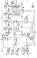
- Figure 1 shows a multi-chip system block diagram configuration in which the invention finds application.
- Four digital logic integrated circuit chips 24A through 24D are connected in cascade fashion for an array processing application. For example, if a 16-point fast Fourier transform were to be performed on data input at the input line 202, the first chip 24A would carry out the first two-point butterfly computation, the results of which would be output on line 202B to the input of the next chip 24B. The chip 24B would then carry out the second two-point butterfly computation the results of which would be output on line 202C to chip 24C. Chip 24C would then carry out the third two-point butterfly computation and output the results on line 202D to the last chip 24D. Chip 24D would carry out the fourth two-point butterfly computation, outputting the results on line 20.
- the group controller 22 is a programmed microprocessor having a control bus 10 connected to each of the digital logic integrated circuit chips 24A through 24D by means of the respective inputs l0A through 10D from the bus 10.
- the bus 10 will pass control information between the group controller 22 and the chips 24A-24D to carry out the necessary arithmetic control functions to coordinate the arithmetic operations of the interdependent chips.
- the bus 10 will also pass testing information between the group controller 22 and the chips 24A-24D to carry out operational tests employing level sensitive scan design techniques (LSSD) during selected testing intervals.
- LSSD level sensitive scan design techniques
- reconfiguration information can be transmitted from the group controller 22 over the bus 10 to the failing chip to control the reconfiguration of the failing chip so that it can operate in a degraded mode to enable the successful production of the desired result, for example the successful completion of the 16-point butterfly computation, described above.
- auxiliary data input line 203A-D can also be employed for selectively routing data around a chip which has failed to the point that it cannot be operated in a degraded mode.
- An auxiliary test input line 14 can be employed to enable specialized testing of the chips 24A-24D during manufacture.
- FIG. 2 illustrates a more detailed view of a single one of the chips 24A-24D, hereinafter designated as chip 24.
- the control bus 10 is composed of seven digital lines, the serial control/test input line 50, the serial control/test output line 52, the type A line 54, the type B line 56, the select line 58, the clock line 60, and the signal out line 62. These lines connect the bus 10 to the monitor 100 on the chip 24, which is. shown in greater det.ail in Figure 3.
- the monitor, circuit 100 serves as the control interface for the chip 24 with respect to the bus 10, and interconnects with a variety of control and arithmetic logic on the chip 24.
- the data bus 202A-D will be referred to hereinafter as the data bus 202 for the generalized chip 24 of Figure 2.
- the data bus 202 consists of eight data lines DO through D7 and the parity line P.
- an odd parity rule is applied so that the total number of binary ones input by the data bus 202 must always be odd, the parity line P assuming a binary zero or a one state in order to comply with this odd parity rule.
- the data input on the data bus 202 is detected to have an even parity where the nine lines have an even number of binary ones therein, it is assumed that a single error has occurred on one of the eight data lines DO through D7.
- Reconfiguration logic 225 on the chip 24 will respond from a command sent from the group controller 22, to reconfigure the data lines DO through D7 and the parity line P so that eight binary bits of valid information will be output on lines 248 to the combinatorial logic functions on the chip 24. Operating under this condition, the chip can no longer benefit from the indication of parity errors on the P line and this mode of operation will be described as the degraded mode of operation.
- the reconfiguration message which controls the reconfiguration logic 225 is received over the bus 10 from the group controller 22 by the monitor 100. This serial-by-bit data input on line 50 is passed through the scan gate 78 to the serial scan string 210 which will convey the reconfiguration message to the reconfiguration shift register 212.
- the reconfiguration decoder 216 in response to the reconfiguration message in the shift register 212, will control the reconfiguration logic 225 to modify the pathways for the parity line P and the one failing data input line among the plurality of input lines DO-D7. This operation is described in conjunction with the description of Figure 4 hereinafter.
- the reconfiguration logic 225 and the reconfiguration decoder 216 comprise a part of the.interface port 200.
- test patterns are input in a serial-by-bit manner on the line 50 to the scan gate 78 of the monitor 100.
- This serial test pattern is output over the serial scan string 210, for example, to the LSSD shift register 104.
- the test pattern bits are then output in parallel over line 111 to the input of the combinatorial logic function 110 and a single cycle of arithmetic operation is carried out.
- the result of that arithmetic operation is output from the logic function 110 on the line 118.to the parallel input of the LSSD shift register 114.
- the result data bits are serially output over line 122 to the serial scan string 112' back to the scan gate 78.
- the test result bits are then serially output over the serial control/test output line 52 to the group.controller 22 where a test result analysis can be conducted.
- Array processing arithmetic operations are typically highly repetitive sequences of elementary arithmetic operations which are performed on large data sets. Such highly repetitive arithmetic operations undergo far fewer branches and interrupts than occur with general purpose computers. This enables the simultaneous execution of sequential portions of the arithmetic operations employing pipelining techniques well-known to the art. This enables a limited repertoire of instruction sets to be made available to the arithmetic logic on a particular integrated circuit chip 24, making it unnecessary to engage in frequent accessing of new instruction sets from an instruction storage device. This enables the use of control parameters which designate which of the limited number of instruction sets are to be executed for a particular array processing arithmetic operation.
- the serial-by-bit level sensitive scan design strings are employed to convey control parameters to the combinatorial logic function blocks on the integrated circuit chip 24 during control setup intervals.
- a control parameter message is input in a serial-by-bit manner on line 50 to the scan gate 78 in the monitor 100.
- the control parameter message is then output on the serial scan string 210, for example, to the serial input of the control parameter shift register 102.
- the control parameter bits are then output in parallel over line 103 to a control input to the combinatorial logic function 110 on the chip 24.
- Additional scan strings, such as 112 can connect additional LSSD shift registers, such as 114, and additional control parameter registers, such as 115, to the scan gate 78.
- the scan gate 78 can selectively connect the scan string 112-112' to the lines 52 and 50. In this manner, efficient usage can be made of the input/output pads on the integrated, circuit chip and the serial scan strings on the integrated circuit chip to enable the combined use of the serial scan strings for a level sensitive scan design testing, for reconfiguration of failing data paths, and for the conveyance of control parameters to combinatorial logic functions on the integrated circuit chip.24.
- a typical integrated digital logic circuit chip 24 can contain as many as 50 000 gates thereon requiring on the order of 1 000 LSSD latches to enable sufficient functional isolation and sufficiently short scan strings to provide reliable testing of the circuitry thereon.
- .Since 200 LSSD latches per scan string is generally considered the limit for practical LSSD testing techniques to be performed, at least five serial scan strings will generally be present on a chip 24 of this example size.
- the scan gate 78 in the monitor 100 is capable of selectively switching between these several lines. This will be described in greater detail hereinafter in connection with the functional block diagram of the monitor 100 shown in Figure 3.
- the monitor 100 shown in Figure 3 has the type A line 54 and the type B line 56 input to the type decoder 55 which has an output to the in gate 51 and the out gate 53.
- the binary values for the signals on the type A line 54 and the type B line 56 signify which of four types of messages is input on the serial control/test input line 50.
- a equals zero and B equals either zero or one the message input on line 50 is a command.
- a equals one and B equals zero the message input on line 50 is an interrupt.
- the message input on line 50 is scan data.
- the in gate 51 in response to the signal from the type decoder 55, will transfer the message input on line 50 to line 82 when the value of A on line 54 is zero.
- the in gate 51 will transfer the message on line 50 to line 86 when the value of A on line 54 is one.and the value of B on line 56 is zero.
- the in gate 51 will transfer the message on line 50 to line 84 when the value of A equals one on line 54 and the value of B equals one on line 56.
- the structure of the monitor 100 in Figure 3 will be described in connection with its function in carrying out three basically different types of operations, changing the control parameter, performing an LSSD test, and carrying out the reconfiguration of data lines in response to a detected parity error.
- a scan string must be selected which includes the control parameter shift register, the arithmetic operations must be stopped, the new control parameter must be scanned in to the control parameter shift register, and then the arithmetic operations restarted. This is achieved in a six step sequence, as follows.
- the signal on the type A line 54 is a binary zero and the signal on the type B line 56 is a binary zero indicating that the message being received on the serial input line 50 is a command.
- the command message is 16 bits long and is transferred by the in gate over line 82-to the instruction register 64.
- the command message has three basic fields, bits 0-through 2 constitute an instruction field, bits 3 through 7 constitute an address field, and bits 8 through 15 constitute a mode field. Bits 0 through 2 are input from the instruction register 64 over the line 66 to the decoder 68.
- Five instructions can be decoded from this field, to load the mode register, to read the status register, to reset the status register, to echo the 16 bits of information in the instruction register 64 through the response register 87 back out onto the output line 52, and a no-op instruction.
- bits ' 0 through 2 designate the loading of the mode register.
- Bits 3 through 7 of the instruction register 64 constitute an address which is decoded by the decoders 90, 72, 95 and 106 to determine which of the respective mode registers 92, 74, 96 or 107 is to receive the mode bits 8 through 15 on line 80.
- the address on line 70 is decoded by the decoder 72 to designate the mode register 74 in the scan section of the monitor as the recipient of bits 8 through 15 on line 80.
- the eight bits loaded into the mode register 74 are decoded by the decoder 76 to select the scan string 210.
- This selection is carried out by the scan gate 78, which connects the data in line 84 from the in gate 51 to the input line of the scan string 210 and which connects the data out line 88 from the output line 210' of the scan string 210 through the out gate 53 to the output line 52.
- the type A line 54 has a binary zero and the type B line 56 has a binary zero,.thereby designating that the serial message input on the data input line 50 is a command.
- the command being received is a stop-on-interrupt command which will serve to stop the arithmetic processing on the integrated circuit chip 24 when an interrupt signal is received.
- This 16-bit command is transferred from the in gate 51 over the line 82 to the instruction register 64. Bits 0 through 2 are decoded by the decoder 68 as an instruction to load the mode register.
- Bits 3 through 7 are decoded by the decoder 106 to designate the mode register 107 in the timing section of the monitor as the recipient of the information in bits 8 through 15. Bits 8 through 15 are output on line 80 to the mode register 107 as a command indicating that when the next interrupt signal is received, the arithmetic processing on the chip will be stopped by the timing control 108.
- the type A line 54 has a binary one value and the type B line 56 has a binary zero value, indicating that the serial message being received on the data input line 50 is an interrupt signal.
- the message on line 50 is transferred by the in gate 51 over the line 86 to the timing control 108 which outputs a stop signal to the arithmetic logic blocks on the chip 24, stopping their operation.
- the type A line 54 has a binary one state and the type B line 56 has a binary one state, designating that the message input on the input line 50 is data.
- The-in gate 51 outputs this message over line 84 to the scan gate 78, which tranfers this data which is a control parameter over the scan line 210 to the control parameter shift register 102 shown in Figure 2.
- a reset'signal on-the chip then causes the parallel output of the control parameter in the shift register 102 to the combinatorial logic block 110, as desired.
- the type A line 54 has a binary zero state and the type B line 56 has a binary zero state, indicating that the message being received on the data line 50 is a command.
- the command message is a run message which will restart the arithmetic processing in the arithmetic logic blocks on the integrated circuit chip 24 upon the receipt of the next interrupt signal.
- the message is transferred from the in gate 51 over the line 82 to the instruction register 64.
- Bits 0 through 2 are decoded by the decoder 68 to indicate to load the mode register.
- the decoder 106 decodes the address on line 70 designating the mode register 107 as the recipient of the message on line 80.
- the run command is loaded in the timing control 108 which will await the next interrupt signal.
- the type A line 54 has a binary one value and the type B line 56 has a binary zero value, indicating that the message being received on the data line 50 is an interrupt signal.
- the interrupt signal is routed by the in gate 51 over the line 86 to the timing control 108 which initiates the restarting of the arithmetic operations by the arithmetic logic functions 110 on the integrated circuit chip 24.
- the LSSD serial scan string 210 on the integrated circuit chip can be employed for changing control parameters governing the logical operation of combinatorial logic functions 110 on the integrated circuit chip.
- the control parameter shift register 115 which is a part of the second scan string 112 can also be operated in the manner described for the control parameter shift register 102.
- a level sensitive scan design (LSSD test) will be conducted by having the group controller 22 transfer an input test pattern over a first serial scan string 210 to a first LSSD shift register 104 for input to the logic function block 110 during a first interval and then, after performing a single logic cycle, the results of processing that test pattern are scanned out from a second LSSD shift register 114 over a second serial scan string 112 back to the group controller 22 for test result analysis.
- LSSD test level sensitive scan design
- the type A line 54 has a binary zero state and the type B line 56 has a binary zero state indicating that the message on the input data line 50 is a command, that command being to select the first scan string 210. That command message is transferred by the in gate 51 over the line .82 to the instruction register 64. Bits 8 through 15 of the message are transferred over line 80 to the mode register 74 and are decoded in the decoder 76 to cause the.scan gate 78 to connect the-scan string 210 to the data in line 84.
- the type A line 54 is a binary zero and the type B line 56 is a binary zero indicating that the message input on the data line 50 is a command, it being a stop-on-interrupt command.
- the command is transferred through the in gate 51 over the line 82 to the instruction register 64.
- Bits 8 through 15 of the command are transferred over line 80 to the mode register 107 and are input to the timing control 108 indicating that a stop signal is to be issued to the logic block 110 upon the receipt of the next interrupt signal.
- the type A line 54 is a binary one state and the type B line 56 is a binary zero state, indicating that the message being received on the data in line 50 is an interrupt signal.
- This interrupt signal is transferred from the in gate 51 over the line 86 to the timing control 108 which then issues a stop signal to the logic function l10 on the integrated circuit chip 24.
- the type A line 54 has a binary' one state and the type B line 56 has a binary one state, indicating that the message being received on the serial data input line 50 is data.
- This is the test pattern data input from the group controller 22 which is to be scanned through the scan gate 78 over the scan line 210 to the LSSD shift register 104.
- the type A line 54 has a binary zero state and the type B line 56 has a binary zero state, indicating that the message being received on the serial data input line 50 is a command, it being a single-cycle-on-interrupt command.
- This command message is transferred over the line 8-2 to the instruction register 64 and bits 8 through 15 are transferred over line 80 to the mode register 107 in the timing section of the monitor.
- This command message is transferred to the timing control 108 so that a single cycle of logic operation will be initiated by the timing control 108 upon the receipt of the next interrupt.
- the type A input 54 is a binary one state and the type B input on line 56 is a binary zero state, indicating that an interrupt signal is being received on the data line 50.
- This signal is transferred by the in gate 51 over the line 86 to the timing control 108.
- the timing control outputs a signal to the logic function 110 causing it to execute a single cycle to perform an arithmetic function on the contents of the LSSD shift register 104 and to output the results of that arithmetic function over line 118 to the output LSSD shift register 114.
- the type A line 54 has a binary zero state and the type B line 56 has a binary zero state, indicating that the message input on the serial data line 50 is a command, namely the command to select the scan string 112.
- This command message is transferred by the in gate 51 over line 82 to the instruction register 64 and.bits 8 through 15 of the message are transferred over line 80 to the mode register 74 and are decoded by the decoder 76.
- the decoder 76 outputs control signals to the scan gate 78 to connect the scan string 112 so that the output line 112' of the scan string l12 is connected to the signal out line 88 from the scan gate 78 to the out gate 53 and thence to the serial data output line 52.
- the type A line 54 has a binary one state and the type B line 56 has a binary one state, indicating that data is to be transferred from the scan gate 78 on the data out line 88 through the out gate 53 to the data out line 52.
- Dummy bits are received on the data input line 50 and are transferred by the in gate 51 over the data in line 84 to the scan gate 78 and are passed through the scan string 112.
- the bits input on line 50 could also be test pattern data for a second test to be subsequently performed.
- test result bits in the output LSSD shift register 114 are output over line 122 and over the output 112' of the serial scan string 112 through the scan gate 78 and over the data output line 88 to the out gate 53 and thence to the data output line 52. These test result bits are then received by the group controller 22 for subsequent test result analysis.
- the type A line 54 has a binary zero state and the type B line 56 has a binary zero state, indicating that the message being received on the serial data input line 50 is a command message and it is the command to restart the arithmetic operations in the logic block 110 upon receipt of the next interrupt.
- This command is transferred over line 82 to the instruction register 64 and bits 8 through 15 are transferred on line 80 to the mode register 107 which enables the timing control 108 to issue a run signal upon receipt of the next interrupt signal.
- the type A line 54 is a binary one and the type B line 56 is a binary zero, indicating that the message being received on the data input line 50 is an interrupt signal.
- the in gate 51 passes this message over line 86 to the timing control 108.
- the timing control 108 issues a run signal to the logic function block 110 on the chip 24, thereby restarting the arithmetic operations on the chip. In this manner, LSSD testing operations are performed.
- the LSSD shift register 204 which is a part of the scan string 210 can also be operated in the manner described for the LSSD shift register 104.
- Figure 4 shows the reconfiguration logic 225 in the interface port 200.
- the data bus 202 has its lines input to the LSSD shift register 204, and those lines are output from the register 204 through the AND gates 208 to a parity error detector consisting of the exclusive OR gates 222 through 234 which are connected to the data input lines D0 through D7 and the exclusive OR 236 which has an input line connected to the parity line P.
- the other input to the exclusive OR 236 is the output of the exclusive OR gates 222 through 234.
- the output from the exclusive OR 236 is the parity error detection signal and will indicate when a parity error has occurred on the data lines DO through D7 input to the integrated circuit chip 24.
- the signal gate 97 When such a parity error is detected, the signal gate 97 outputs a signal on line 62 which passes over the bus 10 to the group controller 22, indicating the existence of a parity error on the chip 24.
- the group controller 22 will then go through a sequence of tests of the data lines DO through D7, employing the LSSD testing procedure described above in conjunction with LSSD shift registers 204, 104 and/or 114.
- the group controller 22 will output a reconfiguration message to the chip 24 which is executed in the following sequence of steps.
- the type A line 54 has a binary zero state and the type B line 56 has a binary zero state, indicating that a command message is being received on the serial input data line 50, that message being to select the scan line 210.
- the in gate 51 conveys the message on line 82 to the instruction register 64 and bits 8 through 15 of the message are transferred to the mode register 74.
- the mode register 74 outputs the message to the decoder 76 which provides signals to the scan gate 78 for connecting the scan line 210 to the data input line 84.
- the type A line 54 has a binary zero state and the type B line 56 has a binary zero state, indicating that a command message is being received on the serial data input line 50 indicating that the arithmetic block 110 is to stop arithmetic operations upon receipt of the next interrupt.
- the command message is conveyed from the in gate 51 over the line 82 to the instruction register 64 and bits 8 through 15 are transferred over line 80 to the mode register 107 in the timing section.
- the timing control 108 receives the message from the mode register 107 and is prepared to stop the arithmetic operations on the integrated circuit chip 24 upon receipt of the next interrupt signal.
- the type A line 54 has a binary one state and the type B line 56 has a binary zero state, indicating the receipt of an interrupt signal on the serial input data line 50.
- the interrupt signal is transferred from the in gate 51 over line 86 to the timing control 108.
- the timing control 108 issues a stop signal to the logic block 110 to stop the arithmetic functions on the integrated circuit chip 24.
- the type A line 54 has a binary one state and the type B line 56 has a binary one state, indicating that data is being received over the serial data input line 50. That data will be the scan data for reconfiguring the input data lines DO through D7 by means of the reconfiguration logic 225.
- the reconfiguration message is transferred from the input data line 50 through the in gate 51 and over the data in line 84 to the scan gate 78 and out onto the scan line 210 which has been selected.
- the reconfiguration message is serially transferred over the serial scan string 210 through the control parameter shift register 102 and through the LSSD shift register 104 and thence over line 211 to the reconfiguration shift register 212.
- the reconfiguration message is then transferred in parallel from the reconfiguration shift register 212 to the reconfiguration decoder 216 where it will be active to execute the desired reconfiguration of the data lines DO through D7, as will be described hereinafter, by means of the reconfiguration logic 225 shown in Figure 4.
- the type A line 54 has a binary zero state and the type B line 56 has a binary zero state, indicating that a command message is being received on the serial input data line 50, that message being a restart message on the next received interrupt signal.
- the command message is transferred from the in gate 51 over the line 82 to the instruction register 64.
- Bits 8 through 15 are transferred over line 80 to the mode register 107 in the timing section of the monitor.
- the timing control 108 receives these bits from the mode register, 107 and is set up to restart the running of the arithmetic logic in the logic block 110 on the integrated circuit-chip 24 upon receipt of the next interrupt signal.
- the type A line 54 has a binary one state and the type B line 56 has a binary zero state, indicating that an interrupt signal is being received on the serial data input line 50.
- This signal is transferred through the in gate 51 over the line 86 to the timing control 108.
- the timing control 108 outputs a run signal to the arithmetic logic in the logic block 110, recommencing the operation of the arithmetic functions to be performed on the chip.
- the LSSD scan strings on the integrated circuit chip 24 can be employed for transferring reconfiguration messages to reconfiguration logic on the integrated circuit chip in response to the detection of parity errors.
- FIG. 4 illustrates the interface port 200 and features the reconfiguration logic 225.
- a reconfiguration shift register 212 has a serial input 211 which is connected through the LSSD shift register 104 and the control parameter shift register 102 over the scan string 210 to the scan gate 78.
- the reconfiguration shift register 212 has a parallel output to the reconfiguration decoder 216 and it has a serial output 214 to the serial input of the LSSD shift register 204.
- the reconfiguration shift register 212 receives reconfiguration bits at the serial input 211 and provides those reconfiguration bits at its parallel output to the decoder 216.
- the LSSD shift register 204 in the interface port 200 has its serial input 214 connected to the serial output of the shift register 212, a parallel input for receiving the data bus lines 202 comprising the eight data lines DO through D7 and the parity line P.
- the LSSD shift register 204 has a serial output line 210' to the scan gate 78 and the parallel output consisting of the nine lines 206.
- the LSSD shift register 204 selectively transfers operand data from the input data bus 202 to the parallel output 206 during normal operating intervals or it will alternately transfer test pattern data from the serial input line 214 which is part of the scan string 210, to the parallel output 206 during LSSD testing intervals.
- Each of the AND gates 208 has a second input connected to a respective one of nine output lines 218 (0) through 218 (7) and 218 (P) from the reconfiguration decoder 216.
- Each of the AND gates 208 has a respective one of nine output lines 220 (0) through 220 (7) and 220 (P).
- the P line in the input data bus 202 is a parity bit line and the remaining eight lines DO through D7 are data input lines associated with the parity bit line P.
- the exclusive OR gates 222 and 224 have their outputs input to the exclusive OR gate 230.
- the exclusive OR gates 226 and 228 have their outputs input to the exclusive OR gate 232.
- the outputs of the exclusive OR gates 230 and 232 are input to the exclusive OR gate 234.
- the output of the exclusive OR gate 234 is input to the exclusive OR gate 236.
- the other input to the exclusive OR gate 236 is the line 220 (P) which is connected through the AND gate 208 (P) and a line 206 (P) and through the LSSD shift register 204, to the P line of the input data bus 202.
- the parity rule to be followed for the data input bus 202 is odd parity so that the total number of binary ones on the nine lines comprising the data bus 202 must be odd.
- an even number of binary ones must be present on the data lines DO through D7 if no parity errors are to be detected, and thus the output of the exclusive OR gate 234 will always be opposite to the parity line 220 (P).
- the output of the exclusive OR 236 will always be a binary one if no parity errors are present.
- Each respective AND gate 242 has a second input connected over a respective one of the eight lines 240 (0) through 240 (7) through a respective one of the eight inverters 238 (0) through 238 (7) to a respective one of eight outputs 218 (0) through 218. (7) from the reconfiguration decoder 216 in Figure 4.
- the output of each respective AND gate 242 (0) through 242 (7) is connected over a respective one of the eight lines 244 (0) through 244 (7) to a first input of a respective one of the eight OR gates 246 (0) through 246 (7).
- the other input of the respective OR gates 246 is connected to the output line 220 (0) through 220 (7) of a respective one of the AND gates 208 (0) through 208 (7), as is shown in Figure 4.
- the outputs of the OR gates 246 are the respective, isolated, output lines 248 (0) through 248 (7) which are directed to logic function blocks 110 on the chip 24.
- the reconfiguration logic 225 In an example of the operation of the reconfiguration logic 225, assume that the input data line D7 is failing at its input to the chip 24.
- the group controller 22 inputs a reconfiguration message to the reconfiguration shift register 212, as previously described, which is decoded by the reconfiguration decoder 216 to provide enabling signals on lines 218 ( P ), and 218 (0) through 218 (6). No enabling signal is output on line 218 (7). Therefore, the AND gate 208 (7) will have its output line 220 (7) at a binary zero value. Since the eight bits of data and the parity bit on the nine lines of the data bus 202 are valid and self consistent until they reach the chip 24, the output of the exclusive OR gate 236 will be the binary value of the failed line D7.
- the binary zero value on the output line 218 (7) from the reconfiguration decoder 216 will be inverted by the inverter 238 (7) to a binary one value which will enable the AND gate 242 (7), thereby passing the output of the exclusive OR 236 over the line 244 (7) to the input of the OR gate 246 (7).
- the binary one value on all of the other output lines from the reconfiguration decoder 216 will be inverted by the inverters 238 to thereby disable the corresponding AND gates 242.
- the output of the exclusive OR gate 236 which is the binary value of the failed bit line D7 is transferred to the corresponding line 248 (7) while the binary value for the input lines DO through D6 are passed through to the respective lines 248 (0) through 248 (6), so as to fully reconstitute the validity of the eight bits of data which are to be transmitted to the combinatorial logic functions on the integrated circuit chip 24.
- a serial reconfiguration message received from the group controller 22 by the chip 24 on line 50 can be conveyed over the serial scan string 210 to the reconfiguration shift register 212 to carry out the reconfiguration of a failing bit line from the input data bus 202, in response to a detected parity error.
Landscapes
- Engineering & Computer Science (AREA)
- General Engineering & Computer Science (AREA)
- Physics & Mathematics (AREA)
- General Physics & Mathematics (AREA)
- Theoretical Computer Science (AREA)
- Computer Hardware Design (AREA)
- Quality & Reliability (AREA)
- Tests Of Electronic Circuits (AREA)
- Test And Diagnosis Of Digital Computers (AREA)
- Testing Or Measuring Of Semiconductors Or The Like (AREA)
- Semiconductor Integrated Circuits (AREA)
- For Increasing The Reliability Of Semiconductor Memories (AREA)
- Testing Of Individual Semiconductor Devices (AREA)
- Control Of Motors That Do Not Use Commutators (AREA)
- Selective Calling Equipment (AREA)
- Maintenance And Management Of Digital Transmission (AREA)
Priority Applications (1)
| Application Number | Priority Date | Filing Date | Title |
|---|---|---|---|
| AT83108275T ATE64483T1 (de) | 1982-10-29 | 1983-08-23 | Online-monitor. |
Applications Claiming Priority (2)
| Application Number | Priority Date | Filing Date | Title |
|---|---|---|---|
| US437775 | 1982-10-29 | ||
| US06/437,775 US4488259A (en) | 1982-10-29 | 1982-10-29 | On chip monitor |
Publications (3)
| Publication Number | Publication Date |
|---|---|
| EP0111053A2 true EP0111053A2 (fr) | 1984-06-20 |
| EP0111053A3 EP0111053A3 (en) | 1987-05-06 |
| EP0111053B1 EP0111053B1 (fr) | 1991-06-12 |
Family
ID=23737827
Family Applications (1)
| Application Number | Title | Priority Date | Filing Date |
|---|---|---|---|
| EP19830108275 Expired - Lifetime EP0111053B1 (fr) | 1982-10-29 | 1983-08-23 | Moniteur on-line |
Country Status (7)
| Country | Link |
|---|---|
| US (1) | US4488259A (fr) |
| EP (1) | EP0111053B1 (fr) |
| JP (1) | JPS5984539A (fr) |
| AT (1) | ATE64483T1 (fr) |
| CA (1) | CA1191558A (fr) |
| DE (1) | DE3382311D1 (fr) |
| ES (1) | ES526020A0 (fr) |
Cited By (7)
| Publication number | Priority date | Publication date | Assignee | Title |
|---|---|---|---|---|
| EP0196171A2 (fr) * | 1985-03-23 | 1986-10-01 | International Computers Limited | Circuits numériques intégrés |
| EP0209982A2 (fr) * | 1985-07-25 | 1987-01-28 | International Computers Limited | Circuits intégrés numériques |
| FR2603704A1 (fr) * | 1986-09-10 | 1988-03-11 | Philips Nv | Procede pour tester un support portant plusieurs circuits integres a fonctionnement numerique, circuit integre propre a etre monte sur un support a tester ainsi, et support pourvu de plusieurs circuits integres de ce genre |
| EP0303065A1 (fr) * | 1987-08-10 | 1989-02-15 | Siemens Nixdorf Informationssysteme Aktiengesellschaft | Procédé et aménagement de circuit pour modules à semi-conducteurs avec éléments logiques de commutation intégrés en technologie LSI |
| EP0336435A2 (fr) * | 1988-04-08 | 1989-10-11 | Wang Laboratories Inc. | Dispositif et procédé de diagnostic de mémoire |
| EP0565866A2 (fr) * | 1992-03-19 | 1993-10-20 | Nec Corporation | Dispositif de circuit à haute densité d'intégration |
| EP0578540A1 (fr) * | 1992-07-08 | 1994-01-12 | STMicroelectronics S.A. | Procédé pour tester le fonctionnement d'un circuit intégré spécialisé, et circuit intégré spécialisé s'y rapportant |
Families Citing this family (31)
| Publication number | Priority date | Publication date | Assignee | Title |
|---|---|---|---|---|
| JPS62228177A (ja) * | 1986-03-29 | 1987-10-07 | Toshiba Corp | 半導体集積回路用許容入力電圧検査回路 |
| JPS63243890A (ja) * | 1987-03-31 | 1988-10-11 | Toshiba Corp | 半導体集積回路装置 |
| US4847839A (en) * | 1987-08-26 | 1989-07-11 | Honeywell Inc. | Digital registers with serial accessed mode control bit |
| US5535331A (en) * | 1987-09-04 | 1996-07-09 | Texas Instruments Incorporated | Processor condition sensing circuits, systems and methods |
| US6304987B1 (en) | 1995-06-07 | 2001-10-16 | Texas Instruments Incorporated | Integrated test circuit |
| US4980889A (en) * | 1988-12-29 | 1990-12-25 | Deguise Wayne J | Multi-mode testing systems |
| US5167020A (en) * | 1989-05-25 | 1992-11-24 | The Boeing Company | Serial data transmitter with dual buffers operating separately and having scan and self test modes |
| JP3005250B2 (ja) | 1989-06-30 | 2000-01-31 | テキサス インスツルメンツ インコーポレイテツド | バスモニター集積回路 |
| US6675333B1 (en) * | 1990-03-30 | 2004-01-06 | Texas Instruments Incorporated | Integrated circuit with serial I/O controller |
| US5581564A (en) * | 1990-12-18 | 1996-12-03 | Integrated Device Technology, Inc. | Diagnostic circuit |
| US5271019A (en) * | 1991-03-15 | 1993-12-14 | Amdahl Corporation | Scannable system with addressable scan reset groups |
| US5872448A (en) * | 1991-06-18 | 1999-02-16 | Lightspeed Semiconductor Corporation | Integrated circuit architecture having an array of test cells providing full controlability for automatic circuit verification |
| US5517515A (en) * | 1994-08-17 | 1996-05-14 | International Business Machines Corporation | Multichip module with integrated test circuitry disposed within interposer substrate |
| US5821773A (en) * | 1995-09-06 | 1998-10-13 | Altera Corporation | Look-up table based logic element with complete permutability of the inputs to the secondary signals |
| US5969538A (en) | 1996-10-31 | 1999-10-19 | Texas Instruments Incorporated | Semiconductor wafer with interconnect between dies for testing and a process of testing |
| US5869979A (en) * | 1996-04-05 | 1999-02-09 | Altera Corporation | Technique for preconditioning I/Os during reconfiguration |
| US6691267B1 (en) | 1997-06-10 | 2004-02-10 | Altera Corporation | Technique to test an integrated circuit using fewer pins |
| US6314550B1 (en) | 1997-06-10 | 2001-11-06 | Altera Corporation | Cascaded programming with multiple-purpose pins |
| US6408413B1 (en) | 1998-02-18 | 2002-06-18 | Texas Instruments Incorporated | Hierarchical access of test access ports in embedded core integrated circuits |
| US6405335B1 (en) | 1998-02-25 | 2002-06-11 | Texas Instruments Incorporated | Position independent testing of circuits |
| US6184707B1 (en) | 1998-10-07 | 2001-02-06 | Altera Corporation | Look-up table based logic element with complete permutability of the inputs to the secondary signals |
| US7058862B2 (en) | 2000-05-26 | 2006-06-06 | Texas Instruments Incorporated | Selecting different 1149.1 TAP domains from update-IR state |
| US6728915B2 (en) | 2000-01-10 | 2004-04-27 | Texas Instruments Incorporated | IC with shared scan cells selectively connected in scan path |
| US6769080B2 (en) | 2000-03-09 | 2004-07-27 | Texas Instruments Incorporated | Scan circuit low power adapter with counter |
| US6803785B1 (en) * | 2000-06-12 | 2004-10-12 | Altera Corporation | I/O circuitry shared between processor and programmable logic portions of an integrated circuit |
| US6961884B1 (en) | 2000-06-12 | 2005-11-01 | Altera Corporation | JTAG mirroring circuitry and methods |
| US7340596B1 (en) | 2000-06-12 | 2008-03-04 | Altera Corporation | Embedded processor with watchdog timer for programmable logic |
| US7424658B1 (en) | 2002-07-01 | 2008-09-09 | Altera Corporation | Method and apparatus for testing integrated circuits |
| DE102006038428A1 (de) * | 2006-08-17 | 2008-02-21 | Bayerische Motoren Werke Ag | Verfahren zur Programmierung eines Steuergerätes eines Kraftfahrzeugs |
| US8589841B2 (en) * | 2012-04-05 | 2013-11-19 | International Business Machines Corporation | Automatic parity checking identification |
| US11525172B1 (en) | 2021-12-01 | 2022-12-13 | L.E. Jones Company | Nickel-niobium intermetallic alloy useful for valve seat inserts |
Citations (1)
| Publication number | Priority date | Publication date | Assignee | Title |
|---|---|---|---|---|
| US3761695A (en) * | 1972-10-16 | 1973-09-25 | Ibm | Method of level sensitive testing a functional logic system |
Family Cites Families (11)
| Publication number | Priority date | Publication date | Assignee | Title |
|---|---|---|---|---|
| US3631402A (en) * | 1970-03-19 | 1971-12-28 | Ncr Co | Input and output circuitry |
| US3614327A (en) * | 1970-10-05 | 1971-10-19 | Nasa | Data multiplexer using tree switching configuration |
| SE358755B (fr) * | 1972-06-09 | 1973-08-06 | Ericsson Telefon Ab L M | |
| US3935476A (en) * | 1974-12-13 | 1976-01-27 | Mostek Corporation | Combination output/input logic for integrated circuit |
| US4071902A (en) * | 1976-06-30 | 1978-01-31 | International Business Machines Corporation | Reduced overhead for clock testing in a level system scan design (LSSD) system |
| DE2842750A1 (de) * | 1978-09-30 | 1980-04-10 | Ibm Deutschland | Verfahren und anordnung zur pruefung von durch monolithisch integrierten halbleiterschaltungen dargestellten sequentiellen schaltungen |
| GB2030807B (en) * | 1978-10-02 | 1982-11-10 | Ibm | Latch circuit |
| US4293919A (en) * | 1979-08-13 | 1981-10-06 | International Business Machines Corporation | Level sensitive scan design (LSSD) system |
| US4312066A (en) * | 1979-12-28 | 1982-01-19 | International Business Machines Corporation | Diagnostic/debug machine architecture |
| DE3030299A1 (de) * | 1980-08-09 | 1982-04-08 | Ibm Deutschland Gmbh, 7000 Stuttgart | Schieberegister fuer pruef- und test-zwecke |
| US4441075A (en) * | 1981-07-02 | 1984-04-03 | International Business Machines Corporation | Circuit arrangement which permits the testing of each individual chip and interchip connection in a high density packaging structure having a plurality of interconnected chips, without any physical disconnection |
-
1982
- 1982-10-29 US US06/437,775 patent/US4488259A/en not_active Expired - Lifetime
-
1983
- 1983-08-23 AT AT83108275T patent/ATE64483T1/de active
- 1983-08-23 DE DE8383108275T patent/DE3382311D1/de not_active Expired - Fee Related
- 1983-08-23 EP EP19830108275 patent/EP0111053B1/fr not_active Expired - Lifetime
- 1983-08-24 CA CA000435243A patent/CA1191558A/fr not_active Expired
- 1983-09-28 ES ES526020A patent/ES526020A0/es active Granted
- 1983-09-30 JP JP58180867A patent/JPS5984539A/ja active Granted
Patent Citations (1)
| Publication number | Priority date | Publication date | Assignee | Title |
|---|---|---|---|---|
| US3761695A (en) * | 1972-10-16 | 1973-09-25 | Ibm | Method of level sensitive testing a functional logic system |
Non-Patent Citations (2)
| Title |
|---|
| DIGEST OF PAPERS OF THE 1979 IEEE TEST CONFERENCE, 23rd - 25th October 1979, Cherry Hill, New Jersey, US, pages 29-36, IEEE, New York, US; L.A. STOLTE et al.: "Design for testability of the IBM system/38" * |
| IBM TECHNICAL DISCLOSURE BULLETIN, vol. 19, no. 9, February 1977, pages 3341-3343, New York, US; R.L. HESTER et al.: "TIE-UP/TIE-DOWN mechanism for input pins on LSI chips" * |
Cited By (13)
| Publication number | Priority date | Publication date | Assignee | Title |
|---|---|---|---|---|
| EP0196171A3 (en) * | 1985-03-23 | 1989-02-01 | International Computers Limited | Digital integrated circuits |
| EP0196171A2 (fr) * | 1985-03-23 | 1986-10-01 | International Computers Limited | Circuits numériques intégrés |
| EP0209982A2 (fr) * | 1985-07-25 | 1987-01-28 | International Computers Limited | Circuits intégrés numériques |
| EP0209982A3 (en) * | 1985-07-25 | 1989-03-08 | International Computers Limited | Digital integrated circuits |
| NL8602274A (nl) * | 1986-09-10 | 1988-04-05 | Philips Nv | Werkwijze voor het testen van een drager met meerdere digitaal-werkende geintegreerde schakelingen, geintegreerde schakeling geschikt voor het aanbrengen op een aldus te testen drager, en drager voorzien van meerdere van zulke geintegreerde schakelingen. |
| FR2603704A1 (fr) * | 1986-09-10 | 1988-03-11 | Philips Nv | Procede pour tester un support portant plusieurs circuits integres a fonctionnement numerique, circuit integre propre a etre monte sur un support a tester ainsi, et support pourvu de plusieurs circuits integres de ce genre |
| EP0303065A1 (fr) * | 1987-08-10 | 1989-02-15 | Siemens Nixdorf Informationssysteme Aktiengesellschaft | Procédé et aménagement de circuit pour modules à semi-conducteurs avec éléments logiques de commutation intégrés en technologie LSI |
| EP0336435A2 (fr) * | 1988-04-08 | 1989-10-11 | Wang Laboratories Inc. | Dispositif et procédé de diagnostic de mémoire |
| EP0336435A3 (fr) * | 1988-04-08 | 1991-02-27 | Wang Laboratories Inc. | Dispositif et procédé de diagnostic de mémoire |
| EP0565866A2 (fr) * | 1992-03-19 | 1993-10-20 | Nec Corporation | Dispositif de circuit à haute densité d'intégration |
| EP0565866A3 (fr) * | 1992-03-19 | 1997-11-05 | Nec Corporation | Dispositif de circuit à haute densité d'intégration |
| EP0578540A1 (fr) * | 1992-07-08 | 1994-01-12 | STMicroelectronics S.A. | Procédé pour tester le fonctionnement d'un circuit intégré spécialisé, et circuit intégré spécialisé s'y rapportant |
| FR2693574A1 (fr) * | 1992-07-08 | 1994-01-14 | Sgs Thomson Microelectronics | Procédé pour tester le fonctionnement d'un circuit intégré spécialisé, et circuit intégré spécialisé s'y rapportant. |
Also Published As
| Publication number | Publication date |
|---|---|
| JPS5984539A (ja) | 1984-05-16 |
| ES8501936A1 (es) | 1984-12-01 |
| ATE64483T1 (de) | 1991-06-15 |
| JPH0260145B2 (fr) | 1990-12-14 |
| CA1191558A (fr) | 1985-08-06 |
| US4488259A (en) | 1984-12-11 |
| DE3382311D1 (en) | 1991-07-18 |
| EP0111053B1 (fr) | 1991-06-12 |
| ES526020A0 (es) | 1984-12-01 |
| EP0111053A3 (en) | 1987-05-06 |
Similar Documents
| Publication | Publication Date | Title |
|---|---|---|
| US4488259A (en) | On chip monitor | |
| US4621363A (en) | Testing and diagnostic device for digital computers | |
| US4722084A (en) | Array reconfiguration apparatus and methods particularly adapted for use with very large scale integrated circuits | |
| US5001712A (en) | Diagnostic error injection for a synchronous bus system | |
| CA1056458A (fr) | Barre omnibus commune de diagnostic pour la verification d'un ordinateur en fonctionnement | |
| EP0095928B1 (fr) | Appareil de traitement pipe-line ayant une fonction de test | |
| EP0716421B1 (fr) | Procédé pour contrôler une matrice de RAM dynamique | |
| JPH07181231A (ja) | 回路ボード試験システム及びその方法 | |
| JPS61163444A (ja) | デ−タ処理装置のエラ−・テスト装置 | |
| US4422141A (en) | Microprocessor architecture for improved chip testability | |
| US4563736A (en) | Memory architecture for facilitating optimum replaceable unit (ORU) detection and diagnosis | |
| JPS60239836A (ja) | 論理回路の故障診断方式 | |
| JPH07287054A (ja) | 集積回路制御 | |
| US4701917A (en) | Diagnostic circuit | |
| US3649963A (en) | Error detection arrangement for register-to-register data transmission | |
| US5055774A (en) | Integrated circuit integrity testing apparatus | |
| US6256761B1 (en) | Integrated electronic module with hardware error infeed for checking purposes | |
| US5689634A (en) | Three purpose shadow register attached to the output of storage devices | |
| JPS62113075A (ja) | Lsi試験システム | |
| JPS63174141A (ja) | 情報処理装置の試験診断方式 | |
| JPS60252958A (ja) | 論理回路の試験方式 | |
| JPS60239835A (ja) | 論理回路の故障診断方式 | |
| JPS62133534A (ja) | デ−タ処理装置のlsi | |
| JPS61267835A (ja) | デ−タ処理装置 | |
| JPS59206945A (ja) | 制御記憶検査装置 |
Legal Events
| Date | Code | Title | Description |
|---|---|---|---|
| PUAI | Public reference made under article 153(3) epc to a published international application that has entered the european phase |
Free format text: ORIGINAL CODE: 0009012 |
|
| AK | Designated contracting states |
Designated state(s): AT CH DE FR GB IT LI NL SE |
|
| 17P | Request for examination filed |
Effective date: 19840823 |
|
| PUAL | Search report despatched |
Free format text: ORIGINAL CODE: 0009013 |
|
| AK | Designated contracting states |
Kind code of ref document: A3 Designated state(s): AT CH DE FR GB IT LI NL SE |
|
| 17Q | First examination report despatched |
Effective date: 19890317 |
|
| GRAA | (expected) grant |
Free format text: ORIGINAL CODE: 0009210 |
|
| AK | Designated contracting states |
Kind code of ref document: B1 Designated state(s): AT CH DE FR GB IT LI NL SE |
|
| PG25 | Lapsed in a contracting state [announced via postgrant information from national office to epo] |
Ref country code: SE Effective date: 19910612 Ref country code: NL Effective date: 19910612 Ref country code: AT Effective date: 19910612 |
|
| REF | Corresponds to: |
Ref document number: 64483 Country of ref document: AT Date of ref document: 19910615 Kind code of ref document: T |
|
| REF | Corresponds to: |
Ref document number: 3382311 Country of ref document: DE Date of ref document: 19910718 |
|
| ET | Fr: translation filed | ||
| ITF | It: translation for a ep patent filed |
Owner name: IBM - DR. ALFREDO BRAVI |
|
| NLV1 | Nl: lapsed or annulled due to failure to fulfill the requirements of art. 29p and 29m of the patents act | ||
| PGFP | Annual fee paid to national office [announced via postgrant information from national office to epo] |
Ref country code: CH Payment date: 19911126 Year of fee payment: 9 |
|
| PLBE | No opposition filed within time limit |
Free format text: ORIGINAL CODE: 0009261 |
|
| STAA | Information on the status of an ep patent application or granted ep patent |
Free format text: STATUS: NO OPPOSITION FILED WITHIN TIME LIMIT |
|
| 26N | No opposition filed | ||
| PG25 | Lapsed in a contracting state [announced via postgrant information from national office to epo] |
Ref country code: LI Effective date: 19920831 Ref country code: CH Effective date: 19920831 |
|
| REG | Reference to a national code |
Ref country code: CH Ref legal event code: PL |
|
| PGFP | Annual fee paid to national office [announced via postgrant information from national office to epo] |
Ref country code: DE Payment date: 19930824 Year of fee payment: 11 |
|
| PGFP | Annual fee paid to national office [announced via postgrant information from national office to epo] |
Ref country code: FR Payment date: 19940725 Year of fee payment: 12 |
|
| PG25 | Lapsed in a contracting state [announced via postgrant information from national office to epo] |
Ref country code: DE Effective date: 19950503 |
|
| PGFP | Annual fee paid to national office [announced via postgrant information from national office to epo] |
Ref country code: GB Payment date: 19951016 Year of fee payment: 13 |
|
| PG25 | Lapsed in a contracting state [announced via postgrant information from national office to epo] |
Ref country code: FR Effective date: 19960430 |
|
| REG | Reference to a national code |
Ref country code: FR Ref legal event code: ST |
|
| PG25 | Lapsed in a contracting state [announced via postgrant information from national office to epo] |
Ref country code: GB Effective date: 19960823 |
|
| GBPC | Gb: european patent ceased through non-payment of renewal fee |
Effective date: 19960823 |