EP0110701A2 - Circuit tampon d'entrée - Google Patents
Circuit tampon d'entrée Download PDFInfo
- Publication number
- EP0110701A2 EP0110701A2 EP83307239A EP83307239A EP0110701A2 EP 0110701 A2 EP0110701 A2 EP 0110701A2 EP 83307239 A EP83307239 A EP 83307239A EP 83307239 A EP83307239 A EP 83307239A EP 0110701 A2 EP0110701 A2 EP 0110701A2
- Authority
- EP
- European Patent Office
- Prior art keywords
- circuit
- fet
- input buffer
- source follower
- inverter
- Prior art date
- Legal status (The legal status is an assumption and is not a legal conclusion. Google has not performed a legal analysis and makes no representation as to the accuracy of the status listed.)
- Granted
Links
Images


Classifications
-
- H—ELECTRICITY
- H03—ELECTRONIC CIRCUITRY
- H03K—PULSE TECHNIQUE
- H03K19/00—Logic circuits, i.e. having at least two inputs acting on one output; Inverting circuits
- H03K19/02—Logic circuits, i.e. having at least two inputs acting on one output; Inverting circuits using specified components
- H03K19/08—Logic circuits, i.e. having at least two inputs acting on one output; Inverting circuits using specified components using semiconductor devices
- H03K19/094—Logic circuits, i.e. having at least two inputs acting on one output; Inverting circuits using specified components using semiconductor devices using field-effect transistors
- H03K19/0952—Logic circuits, i.e. having at least two inputs acting on one output; Inverting circuits using specified components using semiconductor devices using field-effect transistors using Schottky type FET MESFET
-
- H—ELECTRICITY
- H03—ELECTRONIC CIRCUITRY
- H03K—PULSE TECHNIQUE
- H03K19/00—Logic circuits, i.e. having at least two inputs acting on one output; Inverting circuits
- H03K19/003—Modifications for increasing the reliability for protection
- H03K19/00369—Modifications for compensating variations of temperature, supply voltage or other physical parameters
- H03K19/00384—Modifications for compensating variations of temperature, supply voltage or other physical parameters in field effect transistor circuits
-
- H—ELECTRICITY
- H03—ELECTRONIC CIRCUITRY
- H03K—PULSE TECHNIQUE
- H03K19/00—Logic circuits, i.e. having at least two inputs acting on one output; Inverting circuits
- H03K19/01—Modifications for accelerating switching
- H03K19/017—Modifications for accelerating switching in field-effect transistor circuits
- H03K19/01707—Modifications for accelerating switching in field-effect transistor circuits in asynchronous circuits
-
- H—ELECTRICITY
- H03—ELECTRONIC CIRCUITRY
- H03K—PULSE TECHNIQUE
- H03K19/00—Logic circuits, i.e. having at least two inputs acting on one output; Inverting circuits
- H03K19/0175—Coupling arrangements; Interface arrangements
- H03K19/0185—Coupling arrangements; Interface arrangements using field effect transistors only
- H03K19/018507—Interface arrangements
- H03K19/018535—Interface arrangements of Schottky barrier type [MESFET]
Definitions
- the present invention relates to input buffer circuits and more particularly to an input buffer circuit for a digital integrated circuit of FETs which can receive ECL level signals.
- Figure 1 of the accompanying drawings shows by way of example a known input buffer circuit of a digital integrated circuit constructed of FETs (field effect transistors).
- This circuit comprises an inverter which consists of normally "on” type FETs Q 3 and Q 4 , and a level shifting circuit which consists of diodes D and a resistor R.
- the level shifting circuit shifts an input level V in in order to convert it into a voltage level capable of switching the inverter of the succeeding stage, that is, a transition logic level.
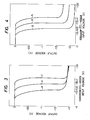
- Figure 2 of the accompanying drawings is a graph of transfer characteristics in Figure 1.
- Curves a, b, and c indicate cases where the ratio W 4/ W 3 between the gate widths of the FETs Q 3 and Q 4 is set at 5, 13 and 50, respectively.
- This graph illustrates the case where a supply voltage V SS is set at -2 V, the threshold voltage V of the FET at -1 V and the level shift magnitude V s of the diodes D at 1.55 V.
- an input logic swing required for satisfactorily switching the output may be smaller as the ratio between the gate width W 4 of the FET Q 4 and the gate width W 3 of the FET Q 3 is greater.
- the output of the inverter needs to be satisfactorily switched in a range of signal levels from - 1.45 V to - 1.15 V. It will be noted from Figure 2 that W 4 /W 3 needs to be at least 13 in order to satisfy the above specification.
- the input buffer of Figure 1 has the following two disadvantages: (a) In the case where the threshold voltage V T of the FET has fluctuated due to dispersions in manufacturing conditions etc., the input logic swing necessary for reliably switching the output increases. . (b) Also in the case where the supply voltage V SS has fluctuated, the input logic swing necessary for reliably switching the output increases.
- Figure 3 of the accompanying drawing is a graph of the transfer characteristics in the case where the threshold voltage V has fluctuated in the circuit of Figure 1
- Figure 4 of the accompanying drawings is a graph of transfer characteristics in the case where the supply voltage V SS has fluctuated in the same circuit.
- the input necessary for reliably switching the output is about -1.6 V as a low level and about -0.9 V as a high level, that is, the logic swing becomes about 0.7 V.
- This value is approximately double that of the input logic swing 0.3 V which is originally required in the absence of any fluctuation, and it becomes a serious problem.
- the value of 0.7 V corresponds to the addition of about 0.4 V which is the width of the change of the input logic threshold value of the inverter, the change being attributed to the fluctuation of the threshold voltage V or the supply voltage V SS .
- a further additional input logic swing of 1.1 V with 0.4 V is required.
- the gate width ratio W 4 /W 3 is set to be smaller, the influence of the fluctuation of the threshold voltage V T is somewhat mitigated, but the input logic swing originally required increases as stated before. It can accordingly be said that, in the presence of the manufacture dispersion or the supply voltage fluctuation, the signal of the ECL level cannot be received by the circuit of Figure 1.
- an input buffer circuit comprising an inverter circuit and a level shifting circuit which shifts an input level in order to convert it to a level capable of switching the inverter, characterized in that said input buffer circuit additionally includes a source follower circuit which having first and second FETs of an identical conductivity type connected in a series, the gate of said first FET being connected to a circuit input for receiving the input signal, the output of the source follower circuit being connected to the inverter through the level shift circuit, a transition logic level of said source follower circuit being controlled by a voltage which is supplied to the gate of said second FET in said source follower circuit.
- the input buffer circuit includes first, second, third and fourth FETs, Q 1 , Q 2 , Q 3 and Q 4 respectively, and diodes- D 2 and a resistor R for level shift.
- Symbols V SS , V SS2 and V LL indicate supply voltages
- symbols V in , V out and V con t indicate voltages at an input terminal, output terminal and control voltage input terminal, respectively.
- the FETs Q 3 and Q 4 constitute an inverter
- the diodes D 2 and the resistor R constitute a level shifting circuit, these elements forming the same circuit as in the prior- art input buffer shown in Figure 1.
- the FETs Q 1 and Q 2 constitute a source follower circuit. Unlike an ordinary source follower circuit, this source follower circuit features that current flowing therethrough can be controlled with the voltage fed to the control voltage input terminal V cont .
- the level shift magnitude of the diodes D 2 will be designated by V S , the source voltage of the FET Q 1 by V 1 , and the gate widths of the FETs Q 1 - Q 4 by W 1 - W 4 respectively.
- V S the source voltage of the FET Q 1 by V 1
- W 1 - W 4 the gate widths of the FETs Q 1 - Q 4 by W 1 - W 4 respectively.
- all the FETs are of the N-channel type and that all the threshold voltages thereof are equal and are V T (V T ⁇ O).
- the supply voltage V SS2 and the threshold voltage V T are selected so as to operate the FETs Q 1 and Q 2 constituting the source follower, in their saturation regions at all times.
- V 1 , V cont and V SS2 Since the saturation condition holds for the FETs Q 1 and Q 2 constituting the source follower, the relationship of Vin. V 1 , V cont and V SS2 becomes as follows:
- V 1 becomes a voltage obtained by converting tne level of the input voltage V. by a certain value which is determined by V T , V SS2 and V cont .
- V 1TH denote the value of V 1 at this time, namely, the input logic threshold value of the inverter
- V 1TH is given by the following equation: Letting V in T H denote the value of V in at this time, namely, the input logic threshold value of the circuit of Figure 5, the following is obtained from equations (1) and (2):
- V in TH can be set at a desired value by selecting the control voltage V cont as follows :
- Figures 6 and 7 are graphs of the transfer characteristics of the circuit in Figure 5, respectively.
- Curves e and f in Figure 6 indicate the transfer characteristics in the cases where the threshold voltage V T has become -1.3 V and -0.7 V, respectively, and curves g and h in Figure T the transfer characteristics in the cases where the supply voltage V SS has become -2.2 V and -1.8 V, respectively.
- V cont as follows: where V T1 , V T2' V T3 and V T4 denote the threshold voltages of the FETs Q 1 , Q 2 , Q 3 and Q 4 , respectively.
- the control circuit includes first, second, third and fourth FETs, Q 1 ', Q 2 ', Q 3 ' and Q 4 ' respectively, and divides D 2 and a resistor R for level shift. Portions constructed of these elements are identical in arrangement to the input buffer of Figure 5, except that the gate of the FET Q 1 ' is supplied with a reference voltage V ref instead of the input voltage V in .
- the circuit also includes an inverter circuit INV.
- the input logic threshold voltage of this inverter circuit INV is designed so as to become a value close to the logic threshold voltage of the output V out of the circuit in Figure 5.
- the circuit includes diodes D, a resistor R * and a supply voltage V LL * , these elements constituting a level shifting circuit for adjusting the output level of the inverter circuit INV to the level of the control voltage Vcont.
- the output V CONT ' of the level shifting circuit is connected to the gate electrode of the FET Q 2 ' so as to apply feedback.
- the output V CONT ' is also a terminal for deriving the control voltage, and it is connected to the control voltage terminal V cont of the input buffer in Figure 5.
- control voltage V CONT ' has become somewhat higher than V cont . Then, current flowing through the N-channel FET Q 2 ' increases to lower V 1 ' and to raise V 2 ', so that the output of the inverter INV becomes close to the low level. Thus, the control voltage V CONT ' lowers.
- control circuit of Figure 8 forms a feedback circuit which functions in the direction of lowering V CONT ' when this voltage has risen. Accordingly, when the control voltage V CONT has conversely become somewhat lower, the output of the inverter INV functionsctions in the direction of raising the control voltage V CONT '. In this way, the control voltage VCONT settles to a value close to V cont' so that the control voltage stable against the fluctuations of the threshold voltage V T , and the supply voltage V SS can be attained.
- FIG 9 is a block diagram showing an embodiment in the case of where the control circuit of Figure 8 is connected to a plurality of input buffers of Figure 5. In this manner the control circuit can also supply a control voltage to a plurality of input buffers.
- the circuit shown in block form in Figure.9 includes an ECL LSI, 10 and a FET LSI 20.
- the circuit further includes output buffers 11, 12 and 13 within the ECL LSI 10, input buffers 14 and 15 within the ECL LSI 10, input buffers 21, 22 and 23 being the same as the one shown in Figure 5, these input buffers being within the FET LSI 20, output buffers 24 and 25 within the FET LSI 20, and a control circuit 26 being the same as that shown in Figure 8.
- the level shift magnitudes of the diodes D 2 in Figure 5 and the diodes D 2 ' in Figure 8 need not be equal to each other. When they are not equal, a voltage obtained by subtracting the difference of the level shift magnitudes from the voltage V inTH may be applied as the reference voltage V ref . It is impossible to make the threshold voltages V T of the respective FETs quite equal.- However; as regards the dispersion of the threshold voltages V T of FETs which are simultaneously manufactured within a single LSI chip, relative fluctuations can be made smaller than absolute fluctuations from a design value.
- the input logic threshold value of the inverter INV has been set at a value close to the transition logic level of the output voltage V out of the circuit in Figure 5.
- the fluctuation of the supply voltage is amplified to change the control voltage V CONT ', and the inverter INV operates as described above.
- the constituent circuits of the inverter INV and the number of constituent stages thereof and the kinds of power sources to be used may may be chosen anyhow. Further, it is sometimes the case that the number of the diodes D changes depending upon the output levels of the inverter INV.
- the output of the inverter INV is directly connected to the control vultage V CONT ' and the gate of the FET Q2', to dispense with the diodes D , resistor R and supply voltage V LL *, or the sense of the diodes D becomes the opposite.
- the supply voltages V SS and V SS2 or the supply voltages V LL and V LL ', V LL may well be equalized.
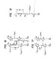
- Figures 10, 11, 12, 13, 14, 15, 16 and 17 are arrangement diagrams of input buffers each showing further embodiments of the present invention.
- the embodiment of Figure 10 is such that, in the arrangement of Figure 5, the level shifting circuit composed of the diodes D 2 , resistor R and voltage source V LL is replaced with diodes D l connected in series between the FETs Q 1 and Q 2 , so as to derive the output of the source follower circuit from between the diodes D 1 and the FET Q 2 and to supply it to the inverter circuit of the succeeding stage.
- the embodiment of Figure 11 is such that, in the arrangement of Figure 5, diodes D 1 are further connected in series between the FETs Q 1 and Q 2 , so as to derive the output of the source follower circuit from between the diodes D 1 and the FET Q 2 and to supply it to the inverter circuit of the succeeding stage through the diodes D 2 .
- the embodiment of Figure 12 is such that, in the arrangement of Figure 5, the level shifting circuit composed of the diodes D 2 , resistor R and voltage source V LL is omitted so as to directly supply the inverter circuit of the succeeding stage with the output of the source follower circuit derived from between the FETs Q 1 and Q 2 .
- the embodiment of Figure 13 is such that, in the arrangement of Figure 11, the FET Q 3 is replaced with a resistor R 3 .
- the embodiments of Figure 14, 15, 16 or 17 are such that, in the arrangements of Figure 5, 10, 11 or 12, a coupling capacitor C is connected between the input end V in (the gate electrode of the FET Q l ) of the source follower circuit and the input end (the gate electrode of the FET Q 4 ) of the inverter circuit, respectively.
- the effect of the present invention is similarly achieved even when the circuit of Figure 5 or the same constituent portions in Figure 8 as in Figure 5 is/are replaced with the circuit shown in Figure 10, 11, 12, 13, 14, 15, 16 or 17.
- the circuit to be used as the input buffer, and the circuit to be used as a part of the control circuit can be selected from among Figures 5, 10, 11, 12, 13, 14, 15, 16 and 17 independently of each other.
- the relations to be met by the FET device constants and circuit constants of the circuit for use as the input buffer and the circuit for use as a part of the control circuit are the same as the relations of equation (6) mentioned before:
- the description thus far made holds as it is by considering the voltage drop V s to be the level shift magnitude of the diodes D 1 for the circuit of Figure 10, to be the sum of the level shift magnitudes of the diodes D 1 and D 2 for the circuit of Figure 11, and to be 0 V for the circuit of Figure 12. It is a matter of course that the number of the diodes D 1 or D 2 in Figure 5, 10, 11, 14,15 or 16 may be any number of at least one.
- the four FETs Q 1 , Q 2 , Q 3 and Q 4 in one input buffer can be brought closer than the distance between the input buffer and the control circuit, the dispersion of the threshold voltages V T can be made still smaller than in the case of the conditions of equation (6). Accordingly, a more remarkable effect can be expected.
- Figure 18 is an arrangement diagram showing another embodiment of the control circuit portion of the present invention.
- any of the level shifting resistors R used in the various embodiments, except the simple control circuit shown in Figure 18, can be replaced with any desired current limiter.
- One example is a FET whose source electrode and gate electrode are connected in common.
- FETs used in the respective embodiments have been of the N-channel, they all may well be P-channel FET S , with the polarities of the diodes and the supply voltages reversed.
- the coupling capacitor C is connected between the input terminal V in and the gate electrode of the FET Q 4 , increase in the delay time can be reduced. Needless to say, the connection of such coupling capacitor C is also applicable to circuits in which the FET Q 3 is replaced with the resistor as shown in Figure 13.
- the control circuit is feared to oscillate. For avoiding this drawback, it is effective to connect a capacitor between the terminal of the control voltage V CONT ' and the power source.
- a signal of any desired level can be received by altering the voltage to be applied as the reference voltage V ref of the control circuit.
- the present invention can realize an input buffer less susceptible to manufacturing dispersions or supply voltage fluctuations, without increasing power consumption or delay time. Therefore, the invention is very effective when applied to any sort of FET integrated . circuit such as GaAs MESFETs or Si MOS devices.
Applications Claiming Priority (2)
| Application Number | Priority Date | Filing Date | Title |
|---|---|---|---|
| JP208301/82 | 1982-11-27 | ||
| JP57208301A JPS5999819A (ja) | 1982-11-27 | 1982-11-27 | 入力インタ−フエイス回路 |
Publications (3)
| Publication Number | Publication Date |
|---|---|
| EP0110701A2 true EP0110701A2 (fr) | 1984-06-13 |
| EP0110701A3 EP0110701A3 (en) | 1985-01-09 |
| EP0110701B1 EP0110701B1 (fr) | 1987-09-30 |
Family
ID=16553980
Family Applications (1)
| Application Number | Title | Priority Date | Filing Date |
|---|---|---|---|
| EP83307239A Expired EP0110701B1 (fr) | 1982-11-27 | 1983-11-28 | Circuit tampon d'entrée |
Country Status (5)
| Country | Link |
|---|---|
| US (1) | US4697110A (fr) |
| EP (1) | EP0110701B1 (fr) |
| JP (1) | JPS5999819A (fr) |
| CA (1) | CA1201179A (fr) |
| DE (1) | DE3373963D1 (fr) |
Cited By (9)
| Publication number | Priority date | Publication date | Assignee | Title |
|---|---|---|---|---|
| WO1987004027A1 (fr) * | 1985-12-20 | 1987-07-02 | Fujitsu Limited | Amplificateur de signaux par tranches utilisant des transistors a effet de champ (fet) |
| US4701643A (en) * | 1986-03-24 | 1987-10-20 | Ford Microelectronics, Inc. | FET gate current limiter circuits |
| US4712023A (en) * | 1985-11-13 | 1987-12-08 | Matsushita Electric Industrial Co., Ltd. | Buffered FET logic gate using depletion-mode MESFET's. |
| EP0284263A1 (fr) * | 1987-03-13 | 1988-09-28 | Gould Electronics Inc. | Circuits logiques FET en cascade |
| EP0314476A2 (fr) * | 1987-10-28 | 1989-05-03 | Gigabit Logic Inc | Compensation de seuil par rétroaction |
| US4877976A (en) * | 1987-03-13 | 1989-10-31 | Gould Inc. | Cascade FET logic circuits |
| EP0349272A2 (fr) * | 1988-06-27 | 1990-01-03 | Nec Corporation | Circuit de conversion de niveau pouvant délivrer des signaux de sortie avec un niveau logique déterminé |
| FR2648643A1 (fr) * | 1989-06-20 | 1990-12-21 | Thomson Composants Microondes | Circuit d'interface entre deux circuits numeriques de natures differentes |
| EP0448269A2 (fr) * | 1990-03-20 | 1991-09-25 | Fujitsu Limited | Circuit d'interface disposé entre un circuit logique à semi-conducteurs composés et un circuit à transistors bipolaires |
Families Citing this family (14)
| Publication number | Priority date | Publication date | Assignee | Title |
|---|---|---|---|---|
| DE3765203D1 (de) * | 1986-07-21 | 1990-10-31 | Siemens Ag | Integrierbare schaltung zur pegelumsetzung. |
| JPH0752837B2 (ja) * | 1987-03-11 | 1995-06-05 | 三菱電機株式会社 | 論理回路 |
| US4798978A (en) * | 1987-04-30 | 1989-01-17 | Gain Electronics Corporation | GAAS FET logic having increased noise margin |
| US4782250A (en) * | 1987-08-31 | 1988-11-01 | International Business Machines Corporation | CMOS off-chip driver circuits |
| US4868427A (en) * | 1987-10-30 | 1989-09-19 | Gazelle Microcircuits, Inc. | ECL to TTL circuit |
| US4814635A (en) * | 1987-11-27 | 1989-03-21 | Motorola, Inc. | Voltage translator circuit |
| JP2574859B2 (ja) * | 1988-03-16 | 1997-01-22 | 株式会社日立製作所 | Fet論理回路 |
| DE4011937A1 (de) * | 1989-04-17 | 1990-10-18 | Mitsubishi Electric Corp | Eingangspufferschaltkreis fuer integrierte halbleiterschaltkreise |
| NL8901170A (nl) * | 1989-05-10 | 1990-12-03 | Philips Nv | Geintegreerde schakeling met een signaalniveauconverter. |
| JPH0567933A (ja) * | 1991-09-06 | 1993-03-19 | Toshiba Corp | レベルシフト回路 |
| JP3315178B2 (ja) * | 1993-02-19 | 2002-08-19 | 三菱電機株式会社 | レベルシフト回路 |
| US6605974B2 (en) * | 2001-07-31 | 2003-08-12 | Telefonaktiebolaget Lm Ericsson(Publ) | Level shifter with gain |
| JP5038710B2 (ja) * | 2006-12-28 | 2012-10-03 | 株式会社日立製作所 | レベル変換回路 |
| WO2011043175A1 (fr) * | 2009-10-09 | 2011-04-14 | Semiconductor Energy Laboratory Co., Ltd. | Circuit logique et écran doté de celui-ci |
Citations (6)
| Publication number | Priority date | Publication date | Assignee | Title |
|---|---|---|---|---|
| FR2230125A1 (en) * | 1973-05-16 | 1974-12-13 | Thomson Csf | Intergrated FET voltage converter with FET in series with resistor - to give constant difference between input and output voltages |
| GB1447476A (en) * | 1972-11-28 | 1976-08-25 | Plessey Co Ltd | Semiconductor circuit arrangements |
| US4242604A (en) * | 1978-08-10 | 1980-12-30 | National Semiconductor Corporation | MOS Input circuit with selectable stabilized trip voltage |
| EP0042777A1 (fr) * | 1980-06-24 | 1981-12-30 | Thomson-Csf | Inverseur logique et opérateur à plusieurs sorties dérivé de cet inverseur utilisant au moins un transistor à effet de champ à faible tension de seuil |
| JPS5750135A (en) * | 1980-09-09 | 1982-03-24 | Nec Corp | Inverter circuit |
| EP0102643A1 (fr) * | 1982-09-06 | 1984-03-14 | Hitachi, Ltd. | Circuit de conversion de niveau |
Family Cites Families (8)
| Publication number | Priority date | Publication date | Assignee | Title |
|---|---|---|---|---|
| US3299291A (en) * | 1964-02-18 | 1967-01-17 | Motorola Inc | Logic elements using field-effect transistors in source follower configuration |
| JPS5845137B2 (ja) * | 1973-05-04 | 1983-10-07 | 株式会社日立製作所 | デンシジユウソウチ |
| US4023050A (en) * | 1976-05-10 | 1977-05-10 | Gte Laboratories Incorporated | Logic level converter |
| FR2469052A1 (fr) * | 1979-11-05 | 1981-05-08 | Thomson Csf | Comparateur a memoire, assurant la regeneration de signaux electriques numeriques, et systeme de transmission numerique utilisant un tel comparateur |
| US4393315A (en) * | 1981-05-18 | 1983-07-12 | Sperry Corporation | High-gain stabilized converter |
| US4453095A (en) * | 1982-07-16 | 1984-06-05 | Motorola Inc. | ECL MOS Buffer circuits |
| US4496856A (en) * | 1982-07-21 | 1985-01-29 | Sperry Corporation | GaAs to ECL level converter |
| US4558235A (en) * | 1983-08-31 | 1985-12-10 | Texas Instruments Incorporated | MESFET logic gate having both DC and AC level shift coupling to the output |
-
1982
- 1982-11-27 JP JP57208301A patent/JPS5999819A/ja active Pending
-
1983
- 1983-11-25 CA CA000442012A patent/CA1201179A/fr not_active Expired
- 1983-11-28 US US06/555,618 patent/US4697110A/en not_active Expired - Fee Related
- 1983-11-28 EP EP83307239A patent/EP0110701B1/fr not_active Expired
- 1983-11-28 DE DE8383307239T patent/DE3373963D1/de not_active Expired
Patent Citations (6)
| Publication number | Priority date | Publication date | Assignee | Title |
|---|---|---|---|---|
| GB1447476A (en) * | 1972-11-28 | 1976-08-25 | Plessey Co Ltd | Semiconductor circuit arrangements |
| FR2230125A1 (en) * | 1973-05-16 | 1974-12-13 | Thomson Csf | Intergrated FET voltage converter with FET in series with resistor - to give constant difference between input and output voltages |
| US4242604A (en) * | 1978-08-10 | 1980-12-30 | National Semiconductor Corporation | MOS Input circuit with selectable stabilized trip voltage |
| EP0042777A1 (fr) * | 1980-06-24 | 1981-12-30 | Thomson-Csf | Inverseur logique et opérateur à plusieurs sorties dérivé de cet inverseur utilisant au moins un transistor à effet de champ à faible tension de seuil |
| JPS5750135A (en) * | 1980-09-09 | 1982-03-24 | Nec Corp | Inverter circuit |
| EP0102643A1 (fr) * | 1982-09-06 | 1984-03-14 | Hitachi, Ltd. | Circuit de conversion de niveau |
Non-Patent Citations (1)
| Title |
|---|
| PATENTS ABSTRACTS OF JAPAN, vol. 6, no. 123 (E-117)[1001], 8th July 1982; & JP - A - 57 050 135 (NIPPON DENKI K.K.) 24-03-1982 * |
Cited By (16)
| Publication number | Priority date | Publication date | Assignee | Title |
|---|---|---|---|---|
| US4712023A (en) * | 1985-11-13 | 1987-12-08 | Matsushita Electric Industrial Co., Ltd. | Buffered FET logic gate using depletion-mode MESFET's. |
| WO1987004027A1 (fr) * | 1985-12-20 | 1987-07-02 | Fujitsu Limited | Amplificateur de signaux par tranches utilisant des transistors a effet de champ (fet) |
| WO1989000359A1 (fr) * | 1985-12-20 | 1989-01-12 | Fujitsu Limited | Amplificateur a tranches utilisant des fet |
| US4701643A (en) * | 1986-03-24 | 1987-10-20 | Ford Microelectronics, Inc. | FET gate current limiter circuits |
| EP0284263A1 (fr) * | 1987-03-13 | 1988-09-28 | Gould Electronics Inc. | Circuits logiques FET en cascade |
| US4877976A (en) * | 1987-03-13 | 1989-10-31 | Gould Inc. | Cascade FET logic circuits |
| EP0314476A2 (fr) * | 1987-10-28 | 1989-05-03 | Gigabit Logic Inc | Compensation de seuil par rétroaction |
| EP0314476A3 (fr) * | 1987-10-28 | 1989-10-11 | Gigabit Logic Inc | Compensation de seuil par rétroaction |
| EP0349272A2 (fr) * | 1988-06-27 | 1990-01-03 | Nec Corporation | Circuit de conversion de niveau pouvant délivrer des signaux de sortie avec un niveau logique déterminé |
| EP0349272A3 (en) * | 1988-06-27 | 1990-08-22 | Nec Corporation | Level conversion circuit having capability of supplying output signal with controlled logical level |
| FR2648643A1 (fr) * | 1989-06-20 | 1990-12-21 | Thomson Composants Microondes | Circuit d'interface entre deux circuits numeriques de natures differentes |
| EP0404634A1 (fr) * | 1989-06-20 | 1990-12-27 | Thomson Composants Microondes | Circuit d'interface entre deux circuits numériques de natures différentes |
| US5045727A (en) * | 1989-06-20 | 1991-09-03 | Thomson Composants Microondes | Interface circuit between two circuits of different logic types |
| EP0448269A2 (fr) * | 1990-03-20 | 1991-09-25 | Fujitsu Limited | Circuit d'interface disposé entre un circuit logique à semi-conducteurs composés et un circuit à transistors bipolaires |
| EP0448269A3 (en) * | 1990-03-20 | 1991-12-11 | Fujitsu Limited | Interface circuit provided between a compound semiconductor logic circuit and a bipolar transistor circuit |
| US5159208A (en) * | 1990-03-20 | 1992-10-27 | Fujitsu Limited | Interface circuit provided between a compound semiconductor logic circuit and a bipolar transistor circuit |
Also Published As
| Publication number | Publication date |
|---|---|
| EP0110701A3 (en) | 1985-01-09 |
| DE3373963D1 (en) | 1987-11-05 |
| JPS5999819A (ja) | 1984-06-08 |
| US4697110A (en) | 1987-09-29 |
| CA1201179A (fr) | 1986-02-25 |
| EP0110701B1 (fr) | 1987-09-30 |
Similar Documents
| Publication | Publication Date | Title |
|---|---|---|
| EP0110701A2 (fr) | Circuit tampon d'entrée | |
| US7148735B2 (en) | Level shifter having automatic delay adjusting function | |
| US4791323A (en) | Level translation circuit | |
| US4380710A (en) | TTL to CMOS Interface circuit | |
| US20050134355A1 (en) | Level shift circuit | |
| KR100591520B1 (ko) | 감소된 전압 입출력의 3상태 버퍼 및 그 제조 방법 | |
| US4563600A (en) | ECL Circuit having a negative feedback differential transistor circuit to increase the operating speed of the output circuit | |
| KR20010049227A (ko) | 레벨조정회로 및 이를 포함하는 데이터 출력회로 | |
| EP0349272A2 (fr) | Circuit de conversion de niveau pouvant délivrer des signaux de sortie avec un niveau logique déterminé | |
| US5565795A (en) | Level converting circuit for reducing an on-quiescence current | |
| US4701643A (en) | FET gate current limiter circuits | |
| US5128556A (en) | Current-switching type logic circuit | |
| KR100251254B1 (ko) | 파워 손실을 절감할 수 있는 전압 감시 회로 | |
| KR900009192B1 (ko) | 차동회로 | |
| US5479116A (en) | Level conversion circuits for converting a digital input signal varying between first and second voltage levels to a digital output signal varying between first and third voltage levels | |
| US10454479B2 (en) | Inverter with balanced voltages across internal transistors | |
| US5160857A (en) | Integratable transistor switch unit of the ntl logic family | |
| US5051626A (en) | Buffer circuit for logic level conversion | |
| KR100759775B1 (ko) | 입출력 버퍼 회로 | |
| EP0365331A1 (fr) | Convertisseur des niveaux ECL/CMOS | |
| US7501873B2 (en) | Digitally controlled threshold adjustment circuit | |
| US7034568B2 (en) | Logic circuit | |
| US5296754A (en) | Push-pull circuit resistant to power supply and temperature induced distortion | |
| US11750098B2 (en) | Voltage conversion circuit having self-adaptive mechanism | |
| US5030854A (en) | Translator circuit for converting ECL type signals to TTL type signals |
Legal Events
| Date | Code | Title | Description |
|---|---|---|---|
| PUAI | Public reference made under article 153(3) epc to a published international application that has entered the european phase |
Free format text: ORIGINAL CODE: 0009012 |
|
| 17P | Request for examination filed |
Effective date: 19840109 |
|
| AK | Designated contracting states |
Designated state(s): DE FR GB NL |
|
| PUAL | Search report despatched |
Free format text: ORIGINAL CODE: 0009013 |
|
| AK | Designated contracting states |
Designated state(s): DE FR GB NL |
|
| 17Q | First examination report despatched |
Effective date: 19860514 |
|
| GRAA | (expected) grant |
Free format text: ORIGINAL CODE: 0009210 |
|
| AK | Designated contracting states |
Kind code of ref document: B1 Designated state(s): DE FR GB |
|
| REF | Corresponds to: |
Ref document number: 3373963 Country of ref document: DE Date of ref document: 19871105 |
|
| ET | Fr: translation filed | ||
| PLBE | No opposition filed within time limit |
Free format text: ORIGINAL CODE: 0009261 |
|
| STAA | Information on the status of an ep patent application or granted ep patent |
Free format text: STATUS: NO OPPOSITION FILED WITHIN TIME LIMIT |
|
| 26N | No opposition filed | ||
| PGFP | Annual fee paid to national office [announced via postgrant information from national office to epo] |
Ref country code: GB Payment date: 19951117 Year of fee payment: 13 |
|
| PGFP | Annual fee paid to national office [announced via postgrant information from national office to epo] |
Ref country code: DE Payment date: 19960129 Year of fee payment: 13 |
|
| PG25 | Lapsed in a contracting state [announced via postgrant information from national office to epo] |
Ref country code: GB Effective date: 19961128 |
|
| GBPC | Gb: european patent ceased through non-payment of renewal fee |
Effective date: 19961128 |
|
| PG25 | Lapsed in a contracting state [announced via postgrant information from national office to epo] |
Ref country code: DE Effective date: 19970801 |
|
| PGFP | Annual fee paid to national office [announced via postgrant information from national office to epo] |
Ref country code: FR Payment date: 19971119 Year of fee payment: 15 |
|
| PG25 | Lapsed in a contracting state [announced via postgrant information from national office to epo] |
Ref country code: FR Free format text: LAPSE BECAUSE OF NON-PAYMENT OF DUE FEES Effective date: 19990730 |
|
| REG | Reference to a national code |
Ref country code: FR Ref legal event code: ST |
|
| PG25 | Lapsed in a contracting state [announced via postgrant information from national office to epo] |
Ref country code: FR Free format text: LAPSE BECAUSE OF NON-PAYMENT OF DUE FEES Effective date: 19971130 |