EP0110353A1 - Bildsignalverarbeitungssystem geeignet für die Darstellung von Halbtonbildern - Google Patents
Bildsignalverarbeitungssystem geeignet für die Darstellung von Halbtonbildern Download PDFInfo
- Publication number
- EP0110353A1 EP0110353A1 EP83111844A EP83111844A EP0110353A1 EP 0110353 A1 EP0110353 A1 EP 0110353A1 EP 83111844 A EP83111844 A EP 83111844A EP 83111844 A EP83111844 A EP 83111844A EP 0110353 A1 EP0110353 A1 EP 0110353A1
- Authority
- EP
- European Patent Office
- Prior art keywords
- picture
- picture information
- color
- circuit means
- signals
- Prior art date
- Legal status (The legal status is an assumption and is not a legal conclusion. Google has not performed a legal analysis and makes no representation as to the accuracy of the status listed.)
- Granted
Links
Images


Classifications
-
- H—ELECTRICITY
- H04—ELECTRIC COMMUNICATION TECHNIQUE
- H04N—PICTORIAL COMMUNICATION, e.g. TELEVISION
- H04N1/00—Scanning, transmission or reproduction of documents or the like, e.g. facsimile transmission; Details thereof
- H04N1/46—Colour picture communication systems
- H04N1/56—Processing of colour picture signals
- H04N1/60—Colour correction or control
- H04N1/6016—Conversion to subtractive colour signals
- H04N1/6019—Conversion to subtractive colour signals using look-up tables
-
- H—ELECTRICITY
- H04—ELECTRIC COMMUNICATION TECHNIQUE
- H04N—PICTORIAL COMMUNICATION, e.g. TELEVISION
- H04N1/00—Scanning, transmission or reproduction of documents or the like, e.g. facsimile transmission; Details thereof
- H04N1/40—Picture signal circuits
- H04N1/40062—Discrimination between different image types, e.g. two-tone, continuous tone
-
- H—ELECTRICITY
- H04—ELECTRIC COMMUNICATION TECHNIQUE
- H04N—PICTORIAL COMMUNICATION, e.g. TELEVISION
- H04N1/00—Scanning, transmission or reproduction of documents or the like, e.g. facsimile transmission; Details thereof
- H04N1/40—Picture signal circuits
- H04N1/405—Halftoning, i.e. converting the picture signal of a continuous-tone original into a corresponding signal showing only two levels
- H04N1/4055—Halftoning, i.e. converting the picture signal of a continuous-tone original into a corresponding signal showing only two levels producing a clustered dots or a size modulated halftone pattern
- H04N1/4058—Halftoning, i.e. converting the picture signal of a continuous-tone original into a corresponding signal showing only two levels producing a clustered dots or a size modulated halftone pattern with details for producing a halftone screen at an oblique angle
-
- H—ELECTRICITY
- H04—ELECTRIC COMMUNICATION TECHNIQUE
- H04N—PICTORIAL COMMUNICATION, e.g. TELEVISION
- H04N1/00—Scanning, transmission or reproduction of documents or the like, e.g. facsimile transmission; Details thereof
- H04N1/46—Colour picture communication systems
- H04N1/52—Circuits or arrangements for halftone screening
-
- H—ELECTRICITY
- H04—ELECTRIC COMMUNICATION TECHNIQUE
- H04N—PICTORIAL COMMUNICATION, e.g. TELEVISION
- H04N1/00—Scanning, transmission or reproduction of documents or the like, e.g. facsimile transmission; Details thereof
- H04N1/46—Colour picture communication systems
- H04N1/56—Processing of colour picture signals
- H04N1/60—Colour correction or control
- H04N1/6016—Conversion to subtractive colour signals
Definitions
- the present invention relates to a picture signal processing system and, more particularly, to a picture signal processing system suitable for displaying continuous tone pictures.
- the display of bi-level pictures is most stable with display devices such as a thermal printer and a liquid crystal display.
- display devices such as a thermal printer and a liquid crystal display.
- continuous tone display system using the dithering method is well known.
- a threshold value for bi-level quantization is fluctuated in accordance with a random or pseudo-random function during the process of quantizing a continuous tone picture to two values.
- the display resolution is reduced and irregular noises are caused when the picture is displayed in various tones.
- a color printer using a color sensor of spatially divided type is well known.
- a color printer when a printed document having characters and a color picture is copied, dots forming the continuous tone color picture are outputed as noise to thereby prevent the colors of the picture from being faithfully reproduced.
- the picture may be blurred by an optical system. When it is done so, however, even the characters are blurred, thus adversely affecting the reproduction of the characters. Blurred picture can also be obtained by an electrical process of averaging picture signals, with the result that small characters cannot be displayed.
- An object of the present invention is to provide a picture information signal processing system suitable for a high-resolution and continuous-tone picture display.
- Another object of the present invention is to provide a picture signal processing system arranged to display a continuous tone color picture without being influenced by pattern noise resulting from dots forming the continuous tone color picture.
- a local fluctuation factor in the density of an input picture is obtained on the basis of a picture information signal so as to display the continuous tone picture. Whe the local fluctuation factor is larger than a predetermined value, bi-level picture inforamtion signals are supplied to a picture output device and, when smaller, dithered picture information signals are supplied to the picture output device.
- a process of averaging color information signals is carried out so that bi-level or dithered signals of the averaged color information signals are supplied to the picture output device.
- a document 1 is illuminated by a line source 2 such as a fluorescent lamp and a picture on the document 1 is imaged on a one-dimensional sensor 4, which has CCD chips, by means of a self-focusing rod-lens array 3 which is known as "SELFOC".
- the document 1 and the optical scanning system are moved relative to each other.
- the optical scanning system is usually moved relative to the document 1.
- Picture signals are read out of the sensor 4 in a serial form and each signal is converted by an A/D converter 5 to a digital signal of eight bits, for example.
- the digital picture signal is applied commonly to density conversion ROMs 6, 7 and 8 provided for corresponding the density characteristic of the document to the density output characteristic of a display printer 22.
- Density conversion tables corresponding to dark, faint and contrastless documents, respectively, are stored in the ROMs 6, 7 and 8.
- the ROMs 6, 7 and 8 are accessed by the digital picture signal from the A/D converter 5 to read out corresponding density-converted picture data.
- One of the ROMs 6, 7 and 8 is selected by a switch 9 in accordance with the density characteristic of the document 1.
- An output signal read out of the selected ROM is applied to a high-frequency component emphasizing circuit or differentiating circuit 10, which generates an output signal (digital) having such a magnitude as corresponds to the local variation factor in the density of the document 1.
- the output signal is used, as will be described later, for switchover between simple two-level display and dithered display of the pictures.
- the differentiating circuit 10 is arranged to perform two-dimensional differentiation of the picture signals using the convolution operation.
- the differentiating circuit 10 comprises a line memory section 11 for preparing two-dimensional picture data corresponding to a two-dimensional picture element array of a predetermined size from one-dimensional input signals, and a sum-of-products operation section 12 for differentiating the two-dimensional data.
- an electrical signal shown in Fig. 2B is obtained from the sensor 4 through the optical system which has transmission characteristics of the rod-lens array 3 and the like.
- this electrical signal is applied to the differentiating circuit 10, a differentiated signal shown in Fig. 2C is obtained..
- This differentiated signal is shown in an analog form in Fig. 2C but practically obtained as a 8-bit digital signal.
- the output signal of the differentiating circuit 10 is applied to a simple binarization/dithering switchover code generator section (ROM) 13.
- This switchover code generator section 13 generates a first code signal "0" to select the simple binarization of picture using a fixed threshold value, when the input signal shown in Fig. 2C has a level larger than a level designated by a broken line 31 or smaller than a level designated by a broken line 32.
- a second code signal "1" is generated to select such organizational dithering of picture as will be described later.
- the switchover code generator section 13 comprises a ROM, whose content may be determined as shown in Fig. 3.
- this ROM is accessed by the differentiated signal to generate a binary signal corresponding to the level of the differentiated signal.
- the local variation factor in the density of the input document is detected by the differentiating cicuit 10 and when the variation factor exceeds the predetermined level, the switchover code generator section 13 generates the code signal for selecting simple binarization of picture, while when the variation factor is lower than the predetermined level, the code signal for selecting dithering of picture.
- the code signal is applied to a multiplexer 14 to select simple bi-level or dithered picture signal.
- a signal on the same line as the output signal of the sum-of-products operation section 12 is derived from the line memory section 11.
- the signal derived from the line memory section 11 is an output signal of the line sensor 4 as shown in Fig. 2B. This signal is subject to the simple binarization or dithered binarization.
- the degradation of high-frequency components of the picture signals cannot be avoided due to transfer characteristics of the optical system including the rod-lens array 3.
- the output signal of the line memory section 11 is corrected by an output signal of the operation circuit 12 which corresponds to the high-frequency components of the picture. Since over-correction brings about a degradation of picture quality, a correcting coefficient K is selected between 0 and 1.
- the output signal of the sum-of-products operation section 12 is multiplied by the correcting coefficient K in a multiplier 15 and applied to an adder 16.
- Time delay is caused in the sum-of-products operation section 12 due to its operation process, so that the output signal of the line memory 11 is supplied to the adder 16 through a delay circuit 17.
- the correcting coefficient K is 1/2 n (n represents an integer)
- the multiplier 15 can be omitted in such a way that the output signal of the sum-of-products operation circuit 12 is added to the corresponding lower significant bits of the output signal of the line memory 11.
- An output signal of the adder 16 is applied to comparators 18 and 19. Picture signals from the adder 16 are compared in the comparator 18 with a fixed threshold value stored in a memory 20 to perform simple binarization of the picture signals. On the other hand, the output signals of the adder 16 are compared every picture element in the comparator 19 with an organic dithering pattern data stored in a memory 21 to obtain dithered binary picture signals.
- Output signals of the comparators 18 and 19 are applied to the selector 14, which is responsive to the selection signal from the ROM 13 to select either of simple binary picture signals or dithered binary picture signals according to the local density variation of the document, the selected picture signal being fed to display printer 22.
- an output picture shown in Fig. 2D can be obtained from an input picture shown in Fig. 2A.
- the output picture shown in Fig. 2D is depicted correspondingly to visible density of the picture.
- Fig. 4A shows a picture signal obtained from the line sensor.
- An output picture as shown in Fig. 4B is obtained from the picture signal by the simple binarization process and, an output picture as shown in Fig. 4C is obtained by the dithered binarization.
- Fig. 2D portions which have a high local density variation factor (or high-frequency components of the picture signal) are displayed as two-level pictures and portions which have a low local density variation factor (or low-frequency components of the picture signal) are displayed as dithered pictures. Therefore, pictures can be displayed with a high resolution and continuous tone picture can be effectively displayed.
- the high-frequency component emphasizing circuit 10 will be described. Irregularity in sensitivity is found among sensing elements or CCD cells of the CCD line sensor 4. When the high-frequency emphasis is performed in the line direction, therefore, the irregularity in sensitivity of the sensing elements will be further enhanced. However, no variation in the sensor output signal is caused in a direction perpendicular to the line sensor, that is, in a direction in which the document is fed or the line sensor is moved. Therefore, a great emphasis of the high-frequency components is possible in the direction perpendicular to the line direction.
- Fig. 5 shows a matrix of parameters for high-frequency emphasis, in which the same parameters are alotted to the first and fifth rows and the same parameters are also alotted to the second and fourth lows.
- Each of the parameters al to c 5 corresponds to a picture element. Data of each of the picture elements in the 5x5 picture elements array is multiplied by its corresponding parameter and the sum of products is found to perform the convolution operation. Picture element data on five lines are simultaneously needed to prepare picture element data for 5x5 picture elements array.
- the line memory section 11 includes six line memories 60a to 60f and a multiplexer 61 and a complex multiplexer 62 arranged at the inputs and outputs of the line memories, respectively.
- the input multiplexer 61 selects the line memories 60a to 60f successively and picture signals are written into the selected line memory from an input terminal I.
- Picture data are simultaneously read out from remaining five line memories to their corresponding output terminals O 1 to 0 5 through the complex multiplexer 62. Every time when one picture element data is written into a selected line memory, five picture element data on the five lines are simultaneously read out from the remaining five line memories, and five consecutive picture element data are successively read out from each of the line memories.
- the output terminals O 1 to 0 5 receive data from five line memories, respectively, in the order of data storage.
- the outputs O 1 to 0 5 of the line memory section 11 are connected to inputs SI 1 to SI 5 of the sum-of-products operation section 12 shown in Fig. 7.
- Picture element data applied to the input SI 1 and SI 5 of the sum-of-products operation section 12 are applied via an adder 70 to a sum-of-products operation circuit 72 where they are multiplied by a corresponding one of parameters a l to a 5 applied from a parameter memory 75, and the resultant products are added together.
- Picture element data applied to the input SI 2 and SI 4 are applied via an adder 71 to a sum-of-products operation circuit 73 where they are multiplied by a corresponding one of parameters b 1 to b 5 applied from a parameter memory 76, the resultant products are added together.
- Picture element data applied to the input SI 3 are supplied to a sum-of-products operation circuit 74 where they are multiplied by a corresponding one of parameters c l to c 5 applied from a parameter memory 77, and the resultant products are added together.
- the outputs of the sum-of-products operation circuits 72 to 74 are connected to an output So via adders 78 and 79.
- a high-frequency component emphasized signal, namely, a differentiated signal is obtained at the output S 0 .
- a picture signal processing system for color picture display will be described.
- separate color signals W, Y' and C' representing white, yellow and cyan picture components, respectively, are provided by a color document input device 80.
- the signals W, Y' and C' are converted to digital signals by A/D converters 81a, 81b and 81c.
- These digital signals are supplied to a color conversion matrix circuit 84 through compensation circuits 83a, 83b and 83c which serve to adapt the input and output characteristics of the input device 80 to the density characteristics of three color inks used in a color printer 82.
- the matrix circuit 84 converts the picture signals W, Y' and C' to color signals M, Y and C according to spectral characteristics of magenta, yellow and cyan inks in the color printer 82.
- the color signals M, Y and C are supplied to picture signal processing circuits 85a, 85b and 85c, respectively, and subject to simple binarization or dithered binarization.
- the picture signal processing circuits have an arrangement identical to that in the above-described embodiment.
- the color picture signals which have been processed as described above are applied to the color printer 82 so that color picture having continuous tones can be obtained with a high resolution.
- a block diagram shown in the picture signal processing circuit 85a is the same as the processing circuit shown in Fig. 1 and corresponding blocks are represented by the same reference numerals. Since the color signals are independently subject to the picture processing of the present invention in this embodiment, fine adjustment of colors is made possible.
- circuits 86a, 86b and 86c similar in function to the ROMs 6, 7 and 8 shown in Fig. 1 may be arranged at the output side of the color conversion matrix circuit 84.
- the separate color signals W, Y' and C' from the input device 80 are converted to digital signals, respectively, by means of the A/D converters 81a, 81b and 81c. These digital signals are applied to logarithmic conversion ROMs 90a, 90b and 90c to be subject to logarithmic conversion to reduce the number of bits of signal.
- the logarithmic- converted digital signals are applied to a color conversion circuit 91, which provides signals M, Y and C.
- the color conversion circuit 91 comprises a RAM (random access memory) in which a color conversion table formed according to the gradation of color which can be displayed by the color printer is stored.
- a color conversion table for converting the color signals W, Y' and C' to the color signals M, Y and C is prepared.
- the bit number of the digital signals W, Y' and C' which access the RAM which stores the conversion table may be smaller than in the embodiment shown in Fig. 8. Since the color conversion circuit 91 comprises the RAM, the content of the color conversion table can be changed.
- This embodiment is provided with a ROM 92 for changing the content of the color conversion table. As in a case where a color input document has a poor contrast or a high density background, color conversion is made possible thanks to this ROM 92, according to the characteristics of the document.
- the selection of the simple binarization or dithered binarization of picture signals is made only on the basis of the picture signal W.
- the signal W is also subject to the simple binarization and dithered binarization.
- the signal W is supplied to a picture signal processing circuit 93 after A/D conversion.
- This circuit 93 is the same as that of Fig. 1 and like blocks are designated by like numerals.
- the output signals M, Y and C of the color conversion circuit 91 are delayed by delay circuits 94a, 94b and 94c correspondingly to the delay caused by the convolution operation in the processing circuit 93, and then subject to simple and dithered binarization processing.
- Numerals 95a, 95b and 95c represent circuits for simple binarization of the signals M, Y and C, respectively, and numerals 96a, 96b and 96c comparators for dithered binarization.
- Numerals 97a, 97b and 97c denote dithering pattern memories for the comparators 96a, 96b and 96c, respectively.
- the simple binary signal and the dithered binary signal of the signal M are applied to a multiplexer 98a.
- the simple binary signal and the dithered binary signal of the signal Y are applied to a multiplexer 98b.
- the like signals of the signal C are applied to a multiplexer 98c.
- the multiplexers 98a, 98b and 98c select one of the simple and dithered binary signals to feed corresponding gate circuits 99a, 99b and 99c.
- An output signal of the multiplexer 14 which selects one of the simple and dithered binary signals of the signal W is applied to a gate circuit 99d.
- a conincidence detecting circuit 100 is provided on the output side of the multiplexers 98a, 98b and 98c to generate an output signal whose logical level is "1", when output levels of the multiplexers 98a, 98b and 98c coincide with one another.
- the gate circuit 99d is enabled by the detected signal of logical level 1 from the coincidence detecting circuit 100 to apply the signal W to a color printer 101. As this time the gate circuits 99a, 99b and 99c are disabled.
- the gate circuit 99d is disabled while the gate circuits 99a to 99c are enabled. Namely, only the signal W is applied to the color printer 101 with respect to the black or white ground of picture, while only the signals M, Y and C are applied to the color printer 101 with respect to the remaining portion of the picture.
- the emphasis of high-frequency components is carried out only with respect to the black and white portions of picture, thus enabling an output picture with a distinct contour to be obtained. Thanks to binarization, linear components can be displayed with high resolution even in color portions except the black and white, and continuous tone color pictures can be pleasantly displayed thanks to dithered binarization.
- Fig. 9 The embodiment of Fig. 9 is arranged such that the signal W (black and white signal) is applied to the color printer as reguired. However, this embodiment may be modified in such a way that the signal W is used only for detecting the local density variation and the color conversion circuit 91 provides a signal B (black) in addition to the signals M, Y and C. This signal B is also subject to the simple and dithered binarization to be applied to the color printer.
- a picture signal processing system of this invention will be described which is arranged to reduce pattern noises resulting from dots of continuous tone picture portions of a color input document.
- Fig. 10 shows a schematic arrangement of a color copying machine wherein a color document is read out by a plurality of CCD chips and a color picture is displayed by the thermal printing method.
- This color copying machine comprises a proximity sensor section 111 which serves as a picture readout device, a color printer section 113, and a picture signal processing section 115 which processes picture signals from the proximity sensor section 111 in accordance with this invention.
- the proximity sensor section 111 comprises an above-described self-focusing rod lens array, a plurality of CCD chips 119a to 119e arranged in the line direction of a document 121 to form a photosensor, and a light source (not shown) for illuminating the document 121.
- the photosensor is of the spatially divided type and six CCD cells, for example, are assigned to a picture element (84 ⁇ m) as shown in Fig. 11. Three pairs of CCD cells each of two adjacent CCD cells have three-color filters W (white), Y (yellow) and C (cyan) thereon, respectively, as shown in Fig. 11. Three color filters may be of Y (yellow), G (green) and C (cyan).
- Picture signals are read out serially from each of the CCD chips 119a to 119e and applied via amplifiers 123a to 123e to A/D converters 125a to 125e, respectively, to be converted to digital signals.
- Signals W, Y and C contained in an output signal of each of the A/D converters 125a to 125e are stored in memories 127, 129 and 131, respectively. It is preferable that each of memories 127, 129 and 131 has a capacity which corresponds to two scanning lines on the document 121.
- Picture signals read out of the memories 127, 129 and 131 are applied to a picture signal processing circuit 133 of the present invention. Output picture signals of the processing circuit 133 are applied to the color thermal printer 113 to form a color output picture by a color sequential system.
- the picture signal processing circuit 133 of this embodiment will be described referring to Fig. 12.
- the signals W, Y and C read out from the memories 127, 129 and 131 are applied to normalization circuits 135a, 135b and 135c, respectively.
- the normalization circuit has a function of eliminating or reducing moire noises which may be caused by a relationship between pitches of picture dots and photosensing elements of the photosensor, and a function of correcting the variation of sensitivity of the photosensing elements or the shading of the photosensor.
- Each of the normalization circuits 135a to 135c includes, as shown in Fig. 13, a register 137 for holding a picture signal detected by one CCD cell only for one clock time, and an adder 139 for adding together two picture signals detected by the two adjacent CCD cells. Bits of output signal of the adder 139 are shifted by one bit to LSB (least significant bit) side, so that an arithmetical mean of two picture signals detected by the two adjacent CCD cells of the same filter color is obtained. This mean signal represents one of separate three color signals for one picture element. When moire components, opposite in sign and substantially same in magnitude, is contained in output signals of the two adjacent CCD cells of the same filter color, they are almost cancelled out by the above-described adding process.
- coordinate transforming circuits 149a, 149b and 149c to correct the subtle color variation caused by this characteristic variation of the color filters and also to reduce the capacity of color conversion table memories for obtaining the signals M, Y and C applied to the color printer.
- FIG. 14 An arrangement of the coordinate transforming circuits 149a to 149c is shown in Fig. 14. Normalized color signals W , Y and C O from the nomalization circuits 135a to 135c are successively applied to a sum-of-products operation circuit 153 via a multiplexer 151. Predetermined coefficients are read out from a coefficient memory 155 and each of the normalized color signals is multiplied by its corresponding coefficient in the sum-of-products operation circuit 153. Three products are added together to provide a coordinate-transformed signal. Coefficient memories 155 for the coordinate transforming circuits 149a to 149c store different coefficients.
- the coordinate transformation of the normalized color signals W O , C O and Y is intended to uniformly distribute, in an address space of a color conversion table memory, address signals (coordinate-transformed signals) for accessing the color conversion table memories which provide the output signals M, C and Y.
- address signals coordinate-transformed signals
- the conversion matrix coefficients become extremely approximate to one another.
- the output signals M, Y and C concentrate within a narrow region in a space represented by the W O , Y O and C o . Therefore, to precisely express each of the output signals necessitates a large number of bits, which results in the complication of the circuit arrangement. If the address signals of the color conversion table memory are uniformly distributed in the address space of this memory, the output signal can be easily represented, resulting in the simplification of the circuit arrangement.
- Brightness signal S 1 and first and second color difference signals S 2 and S 3 are defined from the normalized picture signals W O , Y and C o as follows: S 1 is enough to be defined as a signal corresponding to the brightness signal. S 1 may be W O .
- Equation (2) is expressed in a matrix form as follows:
- Matrix coefficients aij are appropriately selected in such a way that each of the signal X 1 , X 2 and X 3 is uniformly distributed in the address space of the color conversion table memory.
- Sl, S 2 and S 3 are measured from color signals obtained from each of the picture elements each of six CCD cells, and X 1 , X 2 and X 3 are previously determined on the basis of S l , S 2 and S 3 . Therefore, the matrix coefficients can be determined by inverse matrix.
- the matrix coefficients aij are obtained every picture element. Even if S l , S 2 and S 3 are different every picture element, therefore, X l , X 2 and X 3 remain unchanged.
- the coefficient memory 155 stores the matrix coefficients for each of picture elements, which are successively read out, using the computer, to perform coordinate transformation every picture element, thus preventing hue variation of picture elements caused by the variation of the color filter characteristics.
- Matrix coefficients in first, second and third rows of equation (4) are stored in the coefficient memories 155 of the coordinate conversion circuits 149a, 149b and 149c, respectively.
- one picture element is 84 ⁇ m in size and the number of picture elements to be displayed is twelve per 1 mm in the case of color display.
- One picture element is 28 ⁇ m in the case of black and white display, corresponding to 36 picture elements per 1 mm.
- portions such as edges and lines in picture where the variation in density is large is displayed by the normal two levels, and the other portions by the dithering.
- the picture display will be achieved only by the simple binarization even if switchover between simple and dithered binari- zations is carried out with respect to the read out picture signals.
- the switchover of binarization and dithering displays is not based on signal of each picture element, but it is based on an average value of signals which correspond to plural picture elements (e.g. 4x4 or 2x2 picture elements).
- output signals X 1 , X 2 and X 3 of the coordinate transforming circuits 149a to 149c are applied to averaging circuits 157a to 157c, respectively.
- the density variation factor of averaged brightness signal X l is used as a reference for performing the changeover between the binarization and dithering displays. Dot noise is eliminated by the averaging process. The switching between the binarization and dithering displays is carried out on the basis of the brightness signal from which dot noise has been eliminated, thus enabling a clear output picture to be obtained.
- each of the averaging circuits 157a to 157c is enough to average sixteen signals which correspond to 4x4 picture elements.
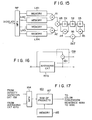
- Fig. 15 show an arrangement of the averaging circuits.
- MP represents a multiplexer, LM 1 to LM 4 line memories each having the same capacity as the number of picture elements on one line, A l to A 6 adders, and D 1 to D 3 delay circuits for delaying signals for one clock time required to transfer one picture element signal.
- Fig. 16 shows a circuit 159 for measuring the local variation of picture density.
- the measuring circuit 159 includes a substracter 161 for calculating the difference between input and output signals of the averaging circuit 157a.
- This substract- ing process is a kind of differentiation, by which the local variation factor can be extremely easily obtained.
- the output signal of the averaging circuit 157a may be differentiated using the circuit shown in Fig. 1.
- Output signals of the averaging circuit 157a and substracter 161 are mixed by a mixer circuit 163.
- output signals of the averaging circuit 157a and substracter 161 are successively applied to a sum-of-products operation circuit 167 via a multiplexer 164.
- the sum-of-products operation circuit 167 matrixes the two input signals, using coefficients stored in a coefficient memory 165, as follows: wherein X represents an input signal of the averaging circuit 157a, X an averaged signal, and a and b matrix coefficients.
- the picture quality of output pictures can be made different from that of input pictures by changing the matrix coefficients.
- a noise-suppressed but somewhat blurred output picture can be obtained by making the coefficient a small and the other coefficient b large.
- an output picture in which the contour of objects is emphasized can be obtained by making the coefficient a large and the other coefficient b small. It is desirable that the coefficients a and b can be changed from outside.
- Output signals of the mixer 163 and averaging circuits 157b and 157c are inputed as address signals to color conversion memories 169a, 169b and 169c.
- Stored in the color conversion memories 169a, 169b and 169c are data on the respective amounts of the inks to print an output picture which are previously calculated according to Neugebauer's equation which is well known in the field of color production.
- An output signal of the local density variation measuring circuit 159 is applied to a binarization/dithering decision section 171, which comprises a ROM, like the above-described embodiment.
- Output signals of the color conversion memories 169a, 169b and 169c are applied to binarization/dithering switching circuits 173a, 173b and 173c.
- the switching circuit comprises a binarization circuit 175a for bi-level quantizing an output signal of the color conversion memory, a dithering reference data memory 177a, a fixed threshold value memory 179a and a multiplexer 181a for selectively connecting one of dithering reference data and fixed threshold value memories 177a and 179a to the binarization circuit 175a in response to the output of the binarization/dithering decision circuit 171.
- the binarization circuit 175a quantizes an input picture signal according to a fixed threshold value stored in the fixed threshold value memory 179a.
- the input picture signal is quantized according to a threshold value set every picture element of the predetermined picture element array and stored in the dithering reference data memory 177a.
- Fig. 19 shows a dithering reference pattern for a 4 x 4 picture-element array. Sixteen picture elements are assigned with priority orders from 1 to 16. Each of picture signals for sixteen picture elements is dithered according to a threshold value which corresponds to the priority order assigned thereto.
- Binary or dithered picture signals extracted from the binarization/dithering switching circuits 173a, 173b and 173c as described above are applied to a thermal head of the color thermal printer.
- the coordinate treansforming circuits 149a, 149b and 149c are provided so that their output signals X i . X 2 and X 3 are adapted to uniformly distribute in address spaces of the color conversion memories 169a, 169b and 169c. Even with such coordinate transforms, however, in the case of a high density (dark) color, it is difficult to differentiate color signals. Dark colors are all converted to black. It is therefore desirable that a non-linear conversion such as a logarithmic conversion be applied to the brightness and color difference signals, particularly to the brightness signal.
- a logarithmic conversion memory 207 is provided on the output side of the mixer 163 for this purpose, as shown in Fig. 20. The output signal of the mixer 163 is applied to the memory 207 as an address signal. Stored in this memory 207 is a color conversion table whose output value remarkably increases as its input address value becomes great.
- Fig. 21 shows an embodiment which is arranged to prevent the generation of such false colors.
- this embodiment when the number of generated false colors exceeds a predetermined number in a region of a predetermined number of picture elements, picture signals are averaged with respect to a larger region of picture elements.
- brightness signal X 1 from the mixer 163 and color difference signals X 2 and X 3 from the average circuits 157b and 157c are applied to a false color detector circuit 209.
- the input signals X 1 , X 2 and X 3 are input to a color detector circuit 211 in the false color dector circuit 209 where it is judged whether or not a color represented by the combination of the signals X i . X 2 and X 3 is present practically.
- the detector circuit 211 is a memory having the same address space as those of the color conversion memories 169a, 169b and 169c but different in the content stored therein.
- the detector circuit 211 when the detector circuit 211 has no address designated by three signals X 1 , X 2 and X 3' it generates an output "1" and when having an address, it generates an output "0". Namely, in case of false color, the memory 211 generates the output "1" which is counted by a counter 213.
- the counter 213 counts the output "1" of the memory 213 every predetermined picture region, that is, during the time a predetermined number of output signals are output from the averaging circuits 157a to 157c.
- the value counted by the counter 213 is compared with a threshold value, which is set by a threshold value circuit 215, by means of a decision circuit 217. When the count value is larger than the threshold value, the decision circuit 217 generates an output "1".
- averaging circuits 157b and 157c On the output side of the averaging circuits 157b and 157c are provided similar averaging circuits 219 and 221.
- a multiplexer 223 is connected to receive output signals of the averaging circuits 157b and 219.
- a multiplexer 225 is connected to receive output signals of the averaging circuits 157c and 221.
- a multiplexer 227 is connected to receive output signals of the averaging circuit 157a and mixer circuit 163. These multiplexers 223, 225 and 227 are controlled by the decision circuit 217.
- the multiplexers 227, 223 and 225 select output signals of the averaging circuits 157a, 157b and 157c, respectively, and supply them to the color conversion memories 169a, 169c and 169c.
- the multiplexers 227, 223 and 225 select output signals of the mixer circuit 163 and averaging circuits 219 and 221, respectively.
- the output of the decision circuit 217 is also connected to multiplexers 181a, 181b and 181c of the binarization/dithering switching circuits 173a, 173b and 173c. Namely, when the output of the decision circuit 217 is "I", the multiplexers 181a, 181b and 181c are caused to select dithered binarization of picture signals.
- Fig. 22 shows an embodiment which is applied to an ordinary printed document having binary pictures such as characters and lines, and a continuous tone picture formed by dot patterns.
- the dot patterns are displayed by dithered binarization of averaged picture signals, and characters and lines by simple binarization of picture signals.
- Fig. 22 input signals of the averaging circuits 157a, 157b and 157c are applied to the false color detector circuit 211.
- the multiplexers 227, 223 and 225 select outputs of the averaging circuits 157a, 157b and 157c, respectively, and connect them to the color conversion memories 169a, 169b and 169c.
- the output of the decision circuit 217 is "1”
- the outputs of the averaging circuits 157a, 157b and 157c are selected respectively.
- the multiplexer 181, dithering reference pattern memory 177 and fixed threshold value memory 179 are provided in common to the binarization circuits 175a, 175b and 175c for binarization of outputs of the color conversion memories 169a, 169b and 169c.
- the multiplexer 181 connects the dithering reference pattern memory 177 to the binarization circuits 175a to 175c to dither output picture signals.
Landscapes
- Engineering & Computer Science (AREA)
- Multimedia (AREA)
- Signal Processing (AREA)
- Facsimile Image Signal Circuits (AREA)
- Image Processing (AREA)
Applications Claiming Priority (4)
| Application Number | Priority Date | Filing Date | Title |
|---|---|---|---|
| JP208474/82 | 1982-11-30 | ||
| JP57208474A JPH0722327B2 (ja) | 1982-11-30 | 1982-11-30 | カラー画像処理装置 |
| JP146532/83 | 1983-08-12 | ||
| JP58146532A JPS6038977A (ja) | 1983-08-12 | 1983-08-12 | 画像信号処理装置 |
Publications (3)
| Publication Number | Publication Date |
|---|---|
| EP0110353A1 true EP0110353A1 (de) | 1984-06-13 |
| EP0110353B1 EP0110353B1 (de) | 1986-06-18 |
| EP0110353B2 EP0110353B2 (de) | 1990-03-21 |
Family
ID=26477344
Family Applications (1)
| Application Number | Title | Priority Date | Filing Date |
|---|---|---|---|
| EP83111844A Expired EP0110353B2 (de) | 1982-11-30 | 1983-11-25 | Bildsignalverarbeitungssystem geeignet für die Darstellung von Halbtonbildern |
Country Status (3)
| Country | Link |
|---|---|
| US (1) | US4663662A (de) |
| EP (1) | EP0110353B2 (de) |
| DE (1) | DE3364212D1 (de) |
Cited By (6)
| Publication number | Priority date | Publication date | Assignee | Title |
|---|---|---|---|---|
| EP0187534A2 (de) * | 1984-12-27 | 1986-07-16 | Kabushiki Kaisha Toshiba | Farbsignalverarbeitungsvorrichtung mit Signalinterpolationsfunktion zum Gebrauch in einem Farbkopiergerät |
| EP0349234A2 (de) * | 1988-06-28 | 1990-01-03 | Fujitsu Limited | Bildverarbeitungssystem |
| EP0365878A2 (de) * | 1988-10-25 | 1990-05-02 | Yozan Inc. | Bildverarbeitungsverfahren |
| EP0415100A2 (de) * | 1989-08-28 | 1991-03-06 | Polaroid Corporation | Eichsystem und -verfahren für Farbbildabtastverfahren |
| EP0588380A2 (de) * | 1988-06-08 | 1994-03-23 | Canon Kabushiki Kaisha | Bildverarbeitungsverfahren |
| NL1012708C2 (nl) * | 1999-07-26 | 2001-01-29 | Ocu Technologies B V | Afdrukken van digitale kleurenbeelden met locaal aangepaste halftoning. |
Families Citing this family (43)
| Publication number | Priority date | Publication date | Assignee | Title |
|---|---|---|---|---|
| FR2542540B1 (fr) * | 1983-03-08 | 1989-02-10 | Canon Kk | Systeme de traitement d'images |
| JPS59205876A (ja) * | 1983-05-10 | 1984-11-21 | Canon Inc | カラー画像処理装置 |
| DE3444366C3 (de) * | 1983-12-09 | 1994-12-22 | Canon Kk | Bildverarbeitungseinrichtung |
| GB2153619B (en) * | 1983-12-26 | 1988-01-20 | Canon Kk | Image processing apparatus |
| JPH0614685B2 (ja) * | 1984-03-29 | 1994-02-23 | 株式会社東芝 | 画像信号処理装置 |
| US4817180A (en) * | 1984-11-10 | 1989-03-28 | Dainippon Screen Mfg. Co., Ltd. | Image signal filtering |
| US5301039A (en) * | 1985-01-21 | 1994-04-05 | Canon Kabushiki Kaisha | Image processing apparatus with pixel tone discrimination |
| JPS61225973A (ja) * | 1985-03-30 | 1986-10-07 | Konishiroku Photo Ind Co Ltd | 多色像形成装置 |
| GB8518026D0 (en) * | 1985-07-17 | 1985-08-21 | British Petroleum Co Plc | Chemical process |
| US4879595A (en) * | 1985-10-22 | 1989-11-07 | Konishiroku Photo Industry Co., Ltd. | Technique for reproducing an image read from a color original |
| DE3637058A1 (de) * | 1985-10-31 | 1987-05-07 | Ricoh Kk | Digitales kopiergeraet |
| US5177795A (en) * | 1985-11-05 | 1993-01-05 | Canon Kabushiki Kaisha | Image processing apparatus |
| US4760463A (en) * | 1985-12-07 | 1988-07-26 | Kabushiki Kaisha Toshiba | Image scanner apparatus with scanning function |
| JPS62243478A (ja) * | 1986-04-16 | 1987-10-23 | Canon Inc | カラ−複写装置 |
| DE3789757T2 (de) * | 1986-05-16 | 1994-08-25 | Canon Kk | Datenübertragungsanlage. |
| US5175635A (en) * | 1986-06-02 | 1992-12-29 | Kabushiki Kaisha Toshiba | Picture printing apparatus using multivalued patterns, binary patterns and dither patterns selectively |
| US4905079A (en) * | 1986-10-28 | 1990-02-27 | Canon Kabushiki Kaisha | Color image processing apparatus for processing separated color signals |
| EP0606962B1 (de) * | 1986-11-14 | 1998-06-03 | Canon Kabushiki Kaisha | Farbbildverarbeitungsgerät |
| US5175807A (en) * | 1986-12-04 | 1992-12-29 | Quantel Limited | Video signal processing with added probabilistic dither |
| US4926251A (en) * | 1987-04-07 | 1990-05-15 | Kabushiki Kaisha Toshiba | Color image processing apparatus with image corrector |
| US4945405A (en) * | 1987-05-21 | 1990-07-31 | Minolta Camera Kabushiki Kaisha | Color image read apparatus with shading and color balance correction |
| JPH06100861B2 (ja) * | 1987-06-03 | 1994-12-12 | コニカ株式会社 | カラ−画像形成装置 |
| US4757389A (en) * | 1987-06-15 | 1988-07-12 | Xerox Corporation | Calibration improvement with dither for a raster input scanner |
| EP0304289A3 (de) * | 1987-08-18 | 1991-03-13 | Kabushiki Kaisha Toshiba | Halbtonbildreproduktionsverfahren und -Gerät |
| JPH01198870A (ja) * | 1987-10-08 | 1989-08-10 | Ricoh Co Ltd | デジタルカラー画像処理装置 |
| DE3839299C2 (de) * | 1987-11-20 | 1995-06-01 | Canon Kk | Bildverarbeitungseinrichtung |
| US5016117A (en) * | 1987-12-29 | 1991-05-14 | Brother Kogyo Kabushiki Kaisha | Optical reader having apparatus for discrimination between dither-matrix and non-dither-matrix reading areas, and/or means for determining light emitter drive power values by using reference reflector surface |
| US5014124A (en) * | 1988-02-25 | 1991-05-07 | Ricoh Company, Ltd. | Digital image processing apparatus |
| JPH01231473A (ja) * | 1988-03-10 | 1989-09-14 | Brother Ind Ltd | 画像形成方法 |
| IT1219118B (it) * | 1988-03-18 | 1990-05-03 | Olivetti & Co Spa | Dispositivo di scansione di documenti per un apparecchiatura di lettura e trattamento digitale di immagini a colori |
| JPH0270173A (ja) * | 1988-09-02 | 1990-03-09 | Fuji Xerox Co Ltd | デジタル画像処理装置 |
| US4956638A (en) * | 1988-09-16 | 1990-09-11 | International Business Machines Corporation | Display using ordered dither |
| JP2791066B2 (ja) * | 1988-11-15 | 1998-08-27 | キヤノン株式会社 | 記録装置 |
| US5121197A (en) * | 1989-02-23 | 1992-06-09 | Minolta Camera Kabushiki Kaisha | Method for processing half tone images to improve efficiency of data compression |
| US4970562A (en) * | 1989-05-22 | 1990-11-13 | Xerox Corporation | Color image processing apparatus |
| JPH0330571A (ja) * | 1989-06-28 | 1991-02-08 | Canon Inc | フアクシミリ装置 |
| CA2020627C (en) | 1989-07-07 | 1995-06-27 | Yuzo Koike | Image processing apparatus |
| JP3028553B2 (ja) * | 1990-04-09 | 2000-04-04 | ソニー株式会社 | 画像処理装置及び画像処理方法 |
| US6906825B1 (en) * | 1999-06-14 | 2005-06-14 | Toshiba Tec Kabushiki Kaisha | Image processor and color image processor |
| JP2001036744A (ja) * | 1999-07-21 | 2001-02-09 | Fujitsu Ltd | 画像読取方法、画像読取装置及び画像処理装置 |
| US6816284B1 (en) * | 2000-04-07 | 2004-11-09 | Color Aix Perts Gmbh | Multispectral color reproduction system with nonlinear coding |
| JP3473600B2 (ja) * | 2000-12-01 | 2003-12-08 | セイコーエプソン株式会社 | 液晶表示装置、画像データ補正回路、画像データ補正方法および電子機器 |
| US20060215929A1 (en) * | 2005-03-23 | 2006-09-28 | David Fresneau | Methods and apparatus for image convolution |
Citations (5)
| Publication number | Priority date | Publication date | Assignee | Title |
|---|---|---|---|---|
| US3937878A (en) | 1975-01-21 | 1976-02-10 | Bell Telephone Laboratories, Incorporated | Animated dithered display systems |
| DE3207079A1 (de) * | 1981-02-27 | 1982-09-16 | Canon K.K., Tokyo | Bildsignalverarbeitungsgeraet |
| DE3226034A1 (de) * | 1981-07-11 | 1983-02-10 | Ricoh Co., Ltd., Tokyo | Verfahren zum verarbeiten eines halbtonbildes |
| DE3225415A1 (de) * | 1981-07-07 | 1983-02-10 | Konishiroku Photo Industry Co., Ltd., Tokyo | Bildaufzeichnungsverfahren und -vorrichtung |
| EP0074794A2 (de) | 1981-09-08 | 1983-03-23 | Xerox Corporation | Apparat und Verfahren zur Erzeugung von Halbtonmuster |
Family Cites Families (15)
| Publication number | Priority date | Publication date | Assignee | Title |
|---|---|---|---|---|
| JPS6035661B2 (ja) * | 1975-09-12 | 1985-08-15 | 大日本スクリーン製造株式会社 | 色修正方法 |
| JPS5537092A (en) * | 1978-09-05 | 1980-03-14 | Ibm | Mode switch for setting threshold value |
| JPS5566174A (en) * | 1978-11-13 | 1980-05-19 | Ricoh Co Ltd | Reproducer of gradation picture |
| US4194221A (en) * | 1978-12-26 | 1980-03-18 | Xerox Corporation | Automatic multimode continuous halftone line copy reproduction |
| US4288821A (en) * | 1980-06-02 | 1981-09-08 | Xerox Corporation | Multi-resolution image signal processing apparatus and method |
| JPS57125580A (en) * | 1981-01-02 | 1982-08-04 | Ibm | Threshould processing mode switch |
| US4554593A (en) * | 1981-01-02 | 1985-11-19 | International Business Machines Corporation | Universal thresholder/discriminator |
| JPS57147376A (en) * | 1981-03-06 | 1982-09-11 | Ricoh Co Ltd | Picture discriminating method |
| JPS583374A (ja) * | 1981-06-29 | 1983-01-10 | Nippon Telegr & Teleph Corp <Ntt> | 中間調処理方式 |
| JPS58153455A (ja) * | 1982-03-06 | 1983-09-12 | Nippon Telegr & Teleph Corp <Ntt> | 中間調信号処理方式 |
| GB2103449B (en) * | 1981-06-29 | 1985-05-30 | Nippon Telegraph & Telephone | Method and apparatus for gray level signal processing |
| JPS5810960A (ja) * | 1981-07-11 | 1983-01-21 | Ricoh Co Ltd | 画信号処理装置 |
| GB2114847B (en) * | 1981-12-26 | 1986-02-12 | Konishiroku Photo Ind | Apparatus for discriminating between linear and tonal picture video signals |
| JPS58142676A (ja) * | 1982-02-18 | 1983-08-24 | Sanyo Electric Co Ltd | カラ−ファクシミリの色変換装置 |
| US4586089A (en) * | 1982-08-18 | 1986-04-29 | Matsushita Electric Industrial Co., Ltd. | Image processor |
-
1983
- 1983-11-25 DE DE8383111844T patent/DE3364212D1/de not_active Expired
- 1983-11-25 EP EP83111844A patent/EP0110353B2/de not_active Expired
- 1983-11-30 US US06/556,323 patent/US4663662A/en not_active Expired - Lifetime
Patent Citations (5)
| Publication number | Priority date | Publication date | Assignee | Title |
|---|---|---|---|---|
| US3937878A (en) | 1975-01-21 | 1976-02-10 | Bell Telephone Laboratories, Incorporated | Animated dithered display systems |
| DE3207079A1 (de) * | 1981-02-27 | 1982-09-16 | Canon K.K., Tokyo | Bildsignalverarbeitungsgeraet |
| DE3225415A1 (de) * | 1981-07-07 | 1983-02-10 | Konishiroku Photo Industry Co., Ltd., Tokyo | Bildaufzeichnungsverfahren und -vorrichtung |
| DE3226034A1 (de) * | 1981-07-11 | 1983-02-10 | Ricoh Co., Ltd., Tokyo | Verfahren zum verarbeiten eines halbtonbildes |
| EP0074794A2 (de) | 1981-09-08 | 1983-03-23 | Xerox Corporation | Apparat und Verfahren zur Erzeugung von Halbtonmuster |
Cited By (13)
| Publication number | Priority date | Publication date | Assignee | Title |
|---|---|---|---|---|
| EP0187534A2 (de) * | 1984-12-27 | 1986-07-16 | Kabushiki Kaisha Toshiba | Farbsignalverarbeitungsvorrichtung mit Signalinterpolationsfunktion zum Gebrauch in einem Farbkopiergerät |
| EP0187534A3 (en) * | 1984-12-27 | 1987-06-03 | Kabushiki Kaisha Toshiba | Color signal processing apparatus with a signal interpolation function for use in a color copier |
| EP0588380A3 (de) * | 1988-06-08 | 1994-04-13 | Canon Kabushiki Kaisha | Bildverarbeitungsverfahren |
| EP0588380A2 (de) * | 1988-06-08 | 1994-03-23 | Canon Kabushiki Kaisha | Bildverarbeitungsverfahren |
| EP0349234A3 (de) * | 1988-06-28 | 1991-04-03 | Fujitsu Limited | Bildverarbeitungssystem |
| EP0349234A2 (de) * | 1988-06-28 | 1990-01-03 | Fujitsu Limited | Bildverarbeitungssystem |
| EP0365878A3 (de) * | 1988-10-25 | 1991-03-20 | Yozan Inc. | Bildverarbeitungsverfahren |
| EP0365878A2 (de) * | 1988-10-25 | 1990-05-02 | Yozan Inc. | Bildverarbeitungsverfahren |
| EP0415100A2 (de) * | 1989-08-28 | 1991-03-06 | Polaroid Corporation | Eichsystem und -verfahren für Farbbildabtastverfahren |
| EP0415100A3 (en) * | 1989-08-28 | 1991-04-10 | Polaroid Corporation | Calibration system and method for color image scanning |
| NL1012708C2 (nl) * | 1999-07-26 | 2001-01-29 | Ocu Technologies B V | Afdrukken van digitale kleurenbeelden met locaal aangepaste halftoning. |
| EP1073261A1 (de) * | 1999-07-26 | 2001-01-31 | Océ-Technologies B.V. | Farbdruck digitaler Bilder mit lokal angepasster Halbtonrasterung |
| US6842268B1 (en) | 1999-07-26 | 2005-01-11 | Oce-Technologies B.V. | Printing of digital color images with locally adjusted half-toning |
Also Published As
| Publication number | Publication date |
|---|---|
| US4663662A (en) | 1987-05-05 |
| DE3364212D1 (en) | 1986-07-24 |
| EP0110353B1 (de) | 1986-06-18 |
| EP0110353B2 (de) | 1990-03-21 |
Similar Documents
| Publication | Publication Date | Title |
|---|---|---|
| EP0110353B1 (de) | Bildsignalverarbeitungssystem geeignet für die Darstellung von Halbtonbildern | |
| US5072291A (en) | Image information signal processing apparatus for improving reproduced image quality by discriminating the type of input image and selecting a particular processing in accordance therewith | |
| US5325448A (en) | Image treatment method and apparatus with error dispersion and controllable quantization | |
| US6118547A (en) | Image processing method and apparatus | |
| EP0187534B1 (de) | Farbsignalverarbeitungsvorrichtung mit Signalinterpolationsfunktion zum Gebrauch in einem Farbkopiergerät | |
| EP0168818B1 (de) | Farbbildkopiergerät | |
| US4414581A (en) | Image signal processing method and apparatus therefor | |
| US5130823A (en) | Error diffusion system | |
| CA2027304A1 (en) | Method and system for reproducing monochromatic and color images using ordered dither and error diffusion | |
| US5515456A (en) | Process for providing digital halftone image with random error diffusion, color correction and enlargement | |
| JPS6198069A (ja) | 画像処理装置 | |
| WO1993022871A1 (en) | Method and system of color halftone reproduction | |
| US5289294A (en) | Image processing apparatus | |
| US7262879B2 (en) | Method for screening of halftone images | |
| EP0707414A2 (de) | Verbessertes Verfahren und Gerät zur Verringerung von Artefakten in Halbtonbildern mit Verwendung von Korrektur des Graugleichgewichts | |
| US5818971A (en) | Method and image reproduction device for reproducing grey values using a combination of error diffusion and cluster dithering for enhanced resolution and tone | |
| US5051841A (en) | Process for providing digital halftone images with random error diffusion | |
| US5303069A (en) | Method for producing a multitone image | |
| US4837846A (en) | Method of the image processing | |
| US6026199A (en) | Method and apparatus for halftoning grey value signals | |
| JPS62149258A (ja) | 画像処理方式 | |
| US6307647B1 (en) | Digital halftoning with error diffusion | |
| US6141121A (en) | Method and apparatus for color halftoning | |
| US5506698A (en) | Image reproducing apparatus and process wherein minimized average error technique is used for each of fractions of original pel intensity value | |
| EP0361538A1 (de) | Verfahren und Anordnung zur Randverstärkung bei der Reproduktion digitalisierter Multipegelbilder durch einen Printer mit konstanter Punktgrösse |
Legal Events
| Date | Code | Title | Description |
|---|---|---|---|
| PUAI | Public reference made under article 153(3) epc to a published international application that has entered the european phase |
Free format text: ORIGINAL CODE: 0009012 |
|
| 17P | Request for examination filed |
Effective date: 19831125 |
|
| AK | Designated contracting states |
Designated state(s): DE FR GB IT NL |
|
| RAP1 | Party data changed (applicant data changed or rights of an application transferred) |
Owner name: KABUSHIKI KAISHA TOSHIBA |
|
| GRAA | (expected) grant |
Free format text: ORIGINAL CODE: 0009210 |
|
| AK | Designated contracting states |
Kind code of ref document: B1 Designated state(s): DE FR GB IT NL |
|
| ITF | It: translation for a ep patent filed |
Owner name: JACOBACCI & PERANI S.P.A. |
|
| REF | Corresponds to: |
Ref document number: 3364212 Country of ref document: DE Date of ref document: 19860724 |
|
| ET | Fr: translation filed | ||
| PLBI | Opposition filed |
Free format text: ORIGINAL CODE: 0009260 |
|
| 26 | Opposition filed |
Opponent name: BSG TECHNISCHE BERATUNGS-GESELLSCHAFT MBH Effective date: 19870318 |
|
| NLR1 | Nl: opposition has been filed with the epo |
Opponent name: BSG TECHNISCHE BERATUNGS-GESELLSCHAFT MBH |
|
| PUAH | Patent maintained in amended form |
Free format text: ORIGINAL CODE: 0009272 |
|
| STAA | Information on the status of an ep patent application or granted ep patent |
Free format text: STATUS: PATENT MAINTAINED AS AMENDED |
|
| 27A | Patent maintained in amended form |
Effective date: 19900321 |
|
| AK | Designated contracting states |
Kind code of ref document: B2 Designated state(s): DE FR GB IT NL |
|
| ITF | It: translation for a ep patent filed |
Owner name: JACOBACCI & PERANI S.P.A. |
|
| NLR2 | Nl: decision of opposition | ||
| ET3 | Fr: translation filed ** decision concerning opposition | ||
| NLR3 | Nl: receipt of modified translations in the netherlands language after an opposition procedure | ||
| ITTA | It: last paid annual fee | ||
| PGFP | Annual fee paid to national office [announced via postgrant information from national office to epo] |
Ref country code: FR Payment date: 19941109 Year of fee payment: 12 |
|
| PGFP | Annual fee paid to national office [announced via postgrant information from national office to epo] |
Ref country code: GB Payment date: 19941115 Year of fee payment: 12 |
|
| PGFP | Annual fee paid to national office [announced via postgrant information from national office to epo] |
Ref country code: DE Payment date: 19941123 Year of fee payment: 12 |
|
| PGFP | Annual fee paid to national office [announced via postgrant information from national office to epo] |
Ref country code: NL Payment date: 19941130 Year of fee payment: 12 |
|
| PG25 | Lapsed in a contracting state [announced via postgrant information from national office to epo] |
Ref country code: GB Effective date: 19951125 |
|
| PG25 | Lapsed in a contracting state [announced via postgrant information from national office to epo] |
Ref country code: NL Effective date: 19960601 |
|
| GBPC | Gb: european patent ceased through non-payment of renewal fee |
Effective date: 19951125 |
|
| PG25 | Lapsed in a contracting state [announced via postgrant information from national office to epo] |
Ref country code: FR Effective date: 19960731 |
|
| NLV4 | Nl: lapsed or anulled due to non-payment of the annual fee |
Effective date: 19960601 |
|
| PG25 | Lapsed in a contracting state [announced via postgrant information from national office to epo] |
Ref country code: DE Effective date: 19960801 |
|
| REG | Reference to a national code |
Ref country code: FR Ref legal event code: ST |