EP0104765B1 - Substratstruktur für eine Halbleiteranordnung und Verfahren zur Herstellung dieses Substrats - Google Patents
Substratstruktur für eine Halbleiteranordnung und Verfahren zur Herstellung dieses Substrats Download PDFInfo
- Publication number
- EP0104765B1 EP0104765B1 EP83304898A EP83304898A EP0104765B1 EP 0104765 B1 EP0104765 B1 EP 0104765B1 EP 83304898 A EP83304898 A EP 83304898A EP 83304898 A EP83304898 A EP 83304898A EP 0104765 B1 EP0104765 B1 EP 0104765B1
- Authority
- EP
- European Patent Office
- Prior art keywords
- film
- region
- substrate
- groove
- layer
- Prior art date
- Legal status (The legal status is an assumption and is not a legal conclusion. Google has not performed a legal analysis and makes no representation as to the accuracy of the status listed.)
- Expired
Links
Images


Classifications
-
- H—ELECTRICITY
- H10—SEMICONDUCTOR DEVICES; ELECTRIC SOLID-STATE DEVICES NOT OTHERWISE PROVIDED FOR
- H10P—GENERIC PROCESSES OR APPARATUS FOR THE MANUFACTURE OR TREATMENT OF DEVICES COVERED BY CLASS H10
- H10P76/00—Manufacture or treatment of masks on semiconductor bodies, e.g. by lithography or photolithography
- H10P76/40—Manufacture or treatment of masks on semiconductor bodies, e.g. by lithography or photolithography of masks comprising inorganic materials
-
- H—ELECTRICITY
- H10—SEMICONDUCTOR DEVICES; ELECTRIC SOLID-STATE DEVICES NOT OTHERWISE PROVIDED FOR
- H10W—GENERIC PACKAGES, INTERCONNECTIONS, CONNECTORS OR OTHER CONSTRUCTIONAL DETAILS OF DEVICES COVERED BY CLASS H10
- H10W10/00—Isolation regions in semiconductor bodies between components of integrated devices
- H10W10/01—Manufacture or treatment
- H10W10/011—Manufacture or treatment of isolation regions comprising dielectric materials
- H10W10/014—Manufacture or treatment of isolation regions comprising dielectric materials using trench refilling with dielectric materials, e.g. shallow trench isolations
- H10W10/0143—Manufacture or treatment of isolation regions comprising dielectric materials using trench refilling with dielectric materials, e.g. shallow trench isolations comprising concurrently refilling multiple trenches having different shapes or dimensions
-
- H—ELECTRICITY
- H10—SEMICONDUCTOR DEVICES; ELECTRIC SOLID-STATE DEVICES NOT OTHERWISE PROVIDED FOR
- H10W—GENERIC PACKAGES, INTERCONNECTIONS, CONNECTORS OR OTHER CONSTRUCTIONAL DETAILS OF DEVICES COVERED BY CLASS H10
- H10W10/00—Isolation regions in semiconductor bodies between components of integrated devices
- H10W10/01—Manufacture or treatment
- H10W10/011—Manufacture or treatment of isolation regions comprising dielectric materials
- H10W10/014—Manufacture or treatment of isolation regions comprising dielectric materials using trench refilling with dielectric materials, e.g. shallow trench isolations
- H10W10/0145—Manufacture or treatment of isolation regions comprising dielectric materials using trench refilling with dielectric materials, e.g. shallow trench isolations of trenches having shapes other than rectangular or V-shape
-
- H—ELECTRICITY
- H10—SEMICONDUCTOR DEVICES; ELECTRIC SOLID-STATE DEVICES NOT OTHERWISE PROVIDED FOR
- H10W—GENERIC PACKAGES, INTERCONNECTIONS, CONNECTORS OR OTHER CONSTRUCTIONAL DETAILS OF DEVICES COVERED BY CLASS H10
- H10W10/00—Isolation regions in semiconductor bodies between components of integrated devices
- H10W10/10—Isolation regions comprising dielectric materials
- H10W10/17—Isolation regions comprising dielectric materials formed using trench refilling with dielectric materials, e.g. shallow trench isolations
Definitions
- This invention relates to a substrate structure of a semiconductor device especially an integrated circuit semiconductor device in which a plurality of semiconductor elements are incorporated into a single semiconductor substrate, and a method of manufacturing the substrate structure.
- US ⁇ A ⁇ 4 269 636 describes a method of manufacturing a bipolar transistor within a device region laterally isolated by means of a groove, but does not describe such a method leading to a substrate having a substantially flat upper surface.
- a principal object of this invention is to provide a method of manufacturing a substrate structure of a semiconductor device having a higher density of integration than a prior art integrated circuit device by improving the characteristics of the element isolating structure.
- Other objects of this invention are to make it possible to manufacture a substrate structure having a thick field oxidized region and a flat semiconductor substrate surface; to make it possible to simplify the manufacturing steps of preparing a semiconductor substrate having a field oxidized region; to make it possible to manufacture a substrate structure of a semiconductor device capable of withstanding several environmental conditions; and to make it possible to manufacture a substrate structure of a semiconductor device having a lesser number of defects in the element regions caused by stress in an isolating groove and in the field oxide region.
- a method of manufacturing a substrate structure of a semiconductor device comprising an element region (P) and a field oxide region (23) adjacent one another on a substrate (11), and an element isolating structure (20, 24) formed between said element region and said field oxide region in direct contact with said field oxide region and consisting of a groove (11 a) containing insulating material (20), whereby said element region is selectively defined by said field oxide region and said element isolating structure, said method characterized by the steps;
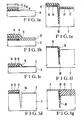
- Figs. 1a through 1g show successive steps of manufacturing a substrate structure of a semiconductor device according to the method of this invention.
- an oxide silicon film 14 having a thickness of about 600 nm by CVD process.
- a photo-resist of a predetermined pattern is applied onto the film 14 and by using the photoresist as a mask, films 14, 13 and 12 are sequentially subjected to reactive etchant, until the substrate 11 is exposed to form interelement isolation pattern shown in Fig. 1a.
- a silicon nitride layer 16' having a thickness of about 300 nm is formed to cover the entire surface by reduced pressure CVD process, for example.
- a silicon nitride region 16 is formed by subjecting the silicon nitride layer 16' to reactive ion etching process using CF 4 gas, for example, until the substrate 11 is exposed. Since reactive ion etching process is used, the flat portion of the silicon nitride layer 16' is removed, so that only the vertical portion along the wall of the interelement isolation pattern is left as the region 16.
- the width of the silicon nitride region 16 formed along the edge of the pattern is substantially equal to the film thickness of the silicon nitride layer 16', that is about 300 nm.
- the thickness of the silicon nitride film 16' is varied to a range between 100 nm and 500 nm when the silicon nitride region 16 is thermal oxidized under this state.
- a silicon oxide film 17 having a thickness of about 300 nm is formed.
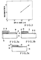
- the silicon oxide film 17 is used as a mask for etching the silicon substrate 11. Then, as shown in Fig. 1d, after removing the silicon nitride region 16 by wet etching utilizing phosphoric acid or the like, the silicon substrate 11 is etched by about 3 micrometers with reactive etching process utilizing SiC1 4 gas, for example to form a groove 11 a. The depth of the groove 11 a formed at this time must be determined by taking account of the breakdown voltage which is required for separating elements in this part.
- Fig. 2 shows a relationship thereabout.
- the silicon substrate used for obtaining this characteristics is n epitaxial layer on a n + doped layer on the surface of p + silicon crystal with the orientation [III]. After forming the groove, a channel cut region may be formed at the bottom of the groove by ion implantation, for example.
- the oxide film 17 on the silicon substrate 11 is removed by etching, and the portion of the silicon substrate 11 underlying the oxide film 17 is etched by a thickness corresponding to 1/2 of that of the field oxide film to be formed later.
- a thermal oxidized film 20' and 17' having a thickness of about 200 nm, and a silicon nitride film 21' having a thickness of about 200 nm is formed by reduced pressure CVD process.
- the silicon nitride film 21' is entirely removed by reactive ion etching process, and the oxide film 17' is removed by wet etching process.
- Fig. 1e the silicon nitride film 21' is entirely removed by reactive ion etching process, and the oxide film 17' is removed by wet etching process.
- the silicon substrate is selectively oxidized to form a field oxide film 23.
- field oxide film means an oxide film formed by oxidizing not only the surface portion of the substrate but also a substantial depth thereof as shown in Fig. 1g. At this time, propagation of oxidation in the lateral direction is prevented by silicon nitride film 21 which also prevents formation of a bird's beak.
- a crystal defect may be formed in the silicon substrate 11. To avoid this, a method shown in Figs. 3a and 3c is used.
- the resist pattern 15 is removed, a silicon nitride film 29 is formed on the entire surface, and then a polycrystalline silicon layer 30 is formed to obtain the structure shown in Fig. 3a.
- a heat oxide silicon film 26, a silicon nitride film 27 formed by CVD technique, a silicon oxide film 28 formed by CVD technique are formed in the left hand portion of a silicon substrate 25.
- a silicon nitride film 29 formed by reduced pressure CVD process is formed on the right hand portion of the substrate 25.
- a polycrystalline silicon layer 30 formed by reduced CVD process is deposited on the silicon nitride film 29 and the silicon-oxide film 28.
- the polycrystalline silicon film 30 may be substituted by any other film having excellent step or edge covering property.
- an oxide film formed by reduced CVD process, a metal film as sputtered aluminum film, or such high polymer film as a photoresist film can be used.
- the polycrystalline film 30 shown in Fig. 3a is etched off except an edge portion 31.
- Fig. 3b the polycrystalline film 30 shown in Fig. 3a is etched off except an edge portion 31.
- the exposed silicon nitride layer 29 is removed by a reactive ion etchant, and a portion 32 covered by the polycrystalline silicon film 31 is left, and thereafter the film 31 is removed. Then, a thermal oxidized silicon film 33 is formed by using the silicon nitride film 32 as a mask.
- the silicon nitride film 32 at the edge may be constituted by any selective oxidation mask. Furthermore, where the oxide film is formed by plasma oxidation or anodic oxidation, the silicon nitride film can be substituted by an alumina film.
- a shallow isolating groove having a depth of less than 1 micrometer as shown in Figs. 4a to 4g can be formed concurrently with formation of a deep groove having a depth of more than 2 micrometers and a field oxide film thicker than 1 micrometer as shown in Fig. 2.
- a thermal oxidized silicon film 35, a silicon nitride film 36 and a CVD silicon oxide film 37 are sequentially formed on a silicon substrate 34 in the order mentioned. Then after applying a photoresist film, the silicon oxide film described above is etched off by a conventional method for forming a groove A having a width of 0.5 micrometer and an edge or step B. Thereafter, as shown in Fig. 4a, a silicon nitride film 39 having a thickness of about 30 to 50 nm and a polycrystalline silicon film 40' having a thickness of about 500 nm are sequentially applied.
- the total thickness H of the silicon oxide film 35, the silicon nitride film 36 and the silicon oxide film 37 on a portion of the surface of the silicon substrate which later becomes an element region should be larger than the width W of the groove.
- the flat portion of the polycrystalline film 40' is removed by dry etching except a polycrystalline region at the edge portion B.
- the exposed silicon nitride film 39 is removed by using a polycrystalline silicon film as a mask.
- a substantial thickness of the polycrystalline silicon film is etched off with a wet etching process to leave only a portion 51 of the polycrystalline silicon film on the surface on which a shallow groove A is to be formed.
- portions other than an element region and an interelement isolating region are oxidized.
- the inner side of the groove A in the polycrystalline silicon layer 51 is oxidized to form a thermal oxidized silicon film 50 and an oxidized polycrystalline silicon film 52.
- the silicon oxide film 50 has a thickness of about 0.4 micrometer, while the silicon oxide film 52 has the same or larger thickness than that of the silicon oxide film 50.
- the assembly is dry etched to form a deep interelement isolating groove 11a a having a depth of about 2 micrometers. Then exposed silicon oxide films 37, 52 and 50 are removed.
- the film 37 is thicker than the other films 52 and 50 a portion thereof is left as a film 41.
- the righthand portion of the substrate 34 thus exposed is etched together with the substrate with the bottom of the shallow groove A exposed by an extent a little smaller than 1/2 of a field oxide film to be formed next.
- a thermal oxidized field film 43 having a thickness of about 1 to 1.5 micrometers is formed on the exposed surface of the substrate 34.
- grooves 11b and 11a a are not completely filled with silicon oxide films, they can be filled with silicon nitride.
- a modification shown in Fig. 1 can be applied to Figs. 4a to 4g.
- Fig. 5 shows a semiconductor device completed in a manner described above, in which 51 represents a silicon substrate, 52 a channel cut P + layer, 53 an n + layer, 54 a field oxide layer, 55 a silicon nitride layer, 56 an n layer, 57 a P + layer, 58 an n + layer, and 59, 60 and 61 base, emitter and collector electrodes respectively.
- a deep groove filled with dielectric and a thick field oxide layer can be formed by self-alignment no bird's beak and bird's head would be formed at the edge of the relatively thick silicon oxide film thus providing an excellent interelement isolation structure for high density integrated circuits with the thick field oxide film in contact with the deep groove.
- the width of the pattern is not limited by the exposure limit of photolithography but can be controlled by the thickness of a film formed by CVD process so that this method is not only suitable for fine construction, but also for deep and shallow grooves filled with dielectric, and a thick field oxide film can be formed by self-alignment. Consequently, the collector compensating region of a bipolar npn transistor constituting an LSI and the base region can be perfectly aligned, thereby providing a structure capable of exhibiting an optimum performance as designed.
- CMOS and Bi-MOS transistors that can be fabricated into a high speed and high density integrated circuit consuming lesser power. By making flat the substrate surface, there is no breakage of the wiring conductors connected later.
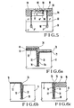
- Figs. 6a through 6c show a modified method of this invention in which the width of the deep groove 11 a is increased and the electric charge stored in the insulating film by radiations is decreased when forming an interelement isolating region.
- elements corresponding to those shown in Fig. 1a to 1g are designated by the same reference characters.
- steps shown in Figs. 6a to 6c only the portions different from Figs. 1a to 1g are shown. Steps up to the step shown in Fig. 6a are the same as those shown in Figs. 1a to 1d, except that the width of the deep groove 11a a is made wider than that shown in Figs. 1a to 1g, by for example 1 micrometer.
- the thickness of the silicon nitride film 16'formed at the step shown in Fig. 1 b should be made large, for example about 0.3 micrometers as described above.
- a channel cut region 70 is formed by implanting boron ions at a dose of 1 x 10 13 /cm 2 and an accelerating voltage of 30 Kv. Then the Si0 2 film on the substrate 11 is etched off and the portion of the silicon substrate 11 underlying this Si0 2 film 17 is etched by a depth corresponding to about 1/2 of a field oxide film to be formed later with reactive ion etching process utilizing SiC 4 gas. Then, the exposed surface of the substrate 11 and the inner surface of the groove 11 a are thermal oxidized to form Si0 2 films 71 and 72 having a thickness of 50 nm, for example.
- a silicon nitride film 73 having a thickness of 150 nm is formed on the entire surfaces of the Si0 2 films 71 and 72 by reduced pressure CVD process. Then a filling member 74 made of polycrystalline silicon semi-insulating material or electroconductive material is formed on the entire surface so as to fill the groove 11 a.
- Fig. 6a shows this state in which the filling member 74 overlies not only the groove 11 a but also the silicon nitride film 73.
- the materials utilized as the filling member 74 are as follows:
- the filling member should have a specific resistance of less than about 10 10 ohm-cm.
- the manufacturing steps of the semiinsulating material is adjusted such that they will have such specific resistivity.
- the flat portion of the filling member 74 is then removed with directive and reactive ion etching process. Consequently, only the portion of the filling material that fills the groove 11 a is left.
- the filled portion 75 has a wedge shape with its upper end rounded.
- the exposed portion of the silicon nitride 73 is removed by a reactive etchant. Thereafter, the exposed oxide films 71 and 14 are etched until the upper surface of the substrate 11 is exposed. This state is shown by Fig. 6b. The right hand portion of the silicon substrate 11 at a lower level is exposed while the left hand portion at a higher level is still covered by the silicon oxide film 12 and the silicon nitride film 13.
- the exposed surface of the silicon substrate 11 is selectively oxidized by pyrogenic oxidation at 900°C, under 8 atmospheric pressure and for 100 minutes to form a field oxide film 76 which is formed to have substantially the same height as the upper surface of the silicon oxide film 12 overlying the silicon substrate 11. Consequently, the upper surface of the silicon substrate is substantially flat.
- the field oxide film 76 When forming the field oxide film, since the layer of Si 3 N 4 is exposed adjacent the groove 11a a on the surface of the silicon substrate 11 at a lower level, and since the surface of the filled portion 75 is inclined downwardly toward right, the field oxide film 76 thus formed completely covers the upper portion of the filled portion 75 so as to form a small recess 78. Accordingly, for the purpose of filling this recess 78, a supplementary filling material such as polycrystalline silicon, semiinsulating material, or electroconductor is applied to cover the entire surface of the substrate. Then the film of the supplementary filling material is etched with directive and reactive ion etchant until the surface of the field oxide film 76 is exposed. Then, as shown in Fig.
- a supplementary filling material such as polycrystalline silicon, semiinsulating material, or electroconductor
- the supplementary filling material also fills the recess 78 so that a portion 79 filled with the supplementary material is formed. Thereafter, exposed Si 3 N 4 film 13 on the portion of the silicon substrate 11 to be used later as the element region is etched off with hot phosphoric acid. For this reason, the groove isolating portion is in direct contact with the thick field oxide film, so that a flat structure can be obtained in which the groove isolating portion, the thick field oxide film and the element region are on the same planes.
- the method of utilizing the filling material can also be applied to a method of manufacturing an LSI wherein an Si0 2 film 72 and/or Si 3 N 4 layer 73 can not be made to be thick for some reasons. More particularly, when the width of the opening of the deep groove amounts to 0.5 to 0.6 micrometers, it is possible to make flat the surfaces of the Si0 2 film and the Si 3 N 4 film without using the filling material when the thicknesses of these films are adjusted more or less. However, due to other limitations of the manufacturing steps there may occur a case in which it is necessary to make thickness of Si0 2 film to be 5000nm (500 angstrom) and that of the Si 3 N 4 film to be 10 micrometers (1000 angstrom). In such a case, openings having width of 20 to 30 micrometers (2000 to 3000 angstroms) could not be filled with these materials, thus forming recesses. The method described above can be used to fill such recesses.
- the electric charge stored in the insulating film can be discharged through conductive filling materials 75 and 79 so that component elements utilized in satellites, for example, and required to have high performances can be obtained under severe environment conditions.
- the field oxide film is in direct contact with the element isolating region (deep groove) it is possible to obtain semiconductor devices suitable to be integrated at high densities. Furthermore even when the isolating groove is in direct contact with the thick field oxide film, there is no fear of forming a step such as a bird's beak, thus obtaining a flat substrate structure, which eliminates the possibility of breaking wiring conductors. Since the field oxide film and the element isolating region are separated by a short (not reaching the surface) Si 3 N 4 film 73, the stress created by the thick field oxide film can be alleviated, thus preventing defects formed in the element region. Accordingly there is no fear of degrading such characteristic as the life of a transistor formed on the element region.
- Figs. 7a and 7b show another modification of this invention in which the method of discharging electric charge from the insulating material shown in Figs. 6a to 6c is applied to the embodiment shown in Figs. 4a to 4g in which a deep groove and a shallow groove are formed simultaneously.
- a shallow groove 11b and a deep groove 11 a are formed in the same manner as in Figs. 4a to 4f.
- a channel cut region 80 is formed at the bottom of the deep groove 11b by ion implantation. This state is shown in Fig. 7a.
- the structure as shown in Fig. 7b is formed by the same steps as those shown in Figs. 6a to 6c. More particularly the entire exposed surface of a silicon substrate 34 is thermal oxidized to form a film of Si0 2 having a thickness of 50 nm, for example. Thereafter, a silicon nitride film 73 having a thickness of 100 nm is formed thereon. At this time, the shallow groove 11b b is completely filled with the oxide film 72 and the silicon nitride film 73. After that, since filling material 74 as polycrystalline silicon, semiinsulating material, or conductive material is applied onto the silicon nitride film 73.
- filling material 74 as polycrystalline silicon, semiinsulating material, or conductive material is applied onto the silicon nitride film 73.
- the filled material 74 is etched off with directive and reactive ion etching technique to remove the flat portion.
- the exposed flat silicon nitride film 73 is removed with a reactive etchants.
- the exposed oxide films 71 and 41 are removed until the silicon substrate 34 is exposed. This state is substantially the same as that shown in Fig. 6b except the shallow groove 11b.
- the surface of the exposed silicon substrate 34 is selectively oxidized to form a field oxidized film 43 with pyrogenic oxidation at 900°C, under a pressure of 8 atmospheric pressure for 100 minutes.
- the field oxide film 43 thus formed overlies the silicon substrate 34 and has the same level as that of the oxide film 35 with the result that the upper surface, as a whole, of the silicon substrate 34 is substantially flat.
- the field oxide film 76 thus formed can not completely cover the upper portion of the filled portion 75 so that a small recess 78 would be formed.
- supplementary filling material as polycrystalline silicon
- semiinsulating material or an electroconductive material is applied to the entire surface of the substrate.
- the supplemen- taryfilling material is etched off with directive and reactive ion etchant until the surface of the field oxide film 71 is exposed. Then as shown in Fig.
- the recess 78 is filled with the supplementary filling material to form a portion 79 filled with the supplementary filling material.
- the exposed Si 3 N 4 layer 36 on the silicon substrate 34 to be used later as the element region is etched off with hot phosphoric acid. In this manner, a flat structure can be obtained including a groove isolating portion, a thick field oxide film and an element region, all lying in the same plane.
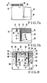
- Figs. 8 and 9 show bipolar transistors prepared by conventional method after removing the oxide film on the surface of the element region by using the method shown in Figs. 7a and 7b.
- the method of this invention can also be applied to form such semiconductor elements as MOS transistors.
- Figs. 8 and 9 show bipolar transistors prepared by conventional method after removing the oxide film on the surface of the element region by using the method shown in Figs. 7a and 7b.
- the method of this invention can also be applied to form such semiconductor elements as MOS transistors.
- 101 represents a P-silicon substrate having a resistivity of 10 to 20 ohm cm and a (111) crystal structure, 102 an n + embedded layer on the substrate 101 and having a surface impurity concentration of about 1 x 10 19 /cm', 103 a P + channel cut region, 104 a filled, oxide film having a thickness of about 1 micrometer, 106 oxide films formed on the inner walls of the deep and shallow grooves for isolating the element, 107 a silicon nitride film overlying the oxide films 106,108 an n type epitaxially grown layer having an impurity concentration of about 1 x 10 16 /cm 3 , 109 a P * diffused layer having an impurity concentration of about 1 x 10 18 / CM 3 , 110 a n diffused layer having an impurity concentration of 1 x 10 18 / CM 3 , 111 to 113 base, emitter and collector electrodes respectively, 115 and 116 a filling material,
- the insulating strength between elements is more than about 3 times of the operating voltage.
- the characteristic shown in Fig. 2 shows that with a groove depth of more than 2.5 micrometers, a reverse breakdown voltage of higher than 20V can be obtained.
- the width of the groove is considerably narrower than that of the prior art element isolating groove, thus enabling to obtain an LSI of high density.
- the surface portion of the silicon substrate at which the field oxide film is to be formed is etched off by a thickness corresponding to about 1/2 of that of the field oxide film to be formed later, it is also possible to etch the exposed surface of the silicon substrate 11 by a thickness corresponding to about 1/2 of that of the field oxide film to be formed to obtain a construction shown in Fig. 10 so as to execute the steps following the step shown in Fig. 1b. In such case, the etching step of the exposed surface of the silicon substrate shown in Fig. 1e becomes unnecessary.
- Fig. 11 shows a modification of the construction shown in Fig. 3a which further comprises an Si0 2 film 130 having a thickness of 70 nm and interposed between the silicon nitride film 29 and the polycrystalline silicon film 30.
- Such multilayer insulation structure can be used, if desired, in the manufacture of semiconductor devices.
- the filling material utilized in Figs. 6a to 6c can be replaced by a simple insulating material such as Si0 2 formed by CVD technique where it is not necessary to have a discharge property.
- a reactive ion etchant is usually used but any other etchant may be used so long as it has a directivity.
- the isolating groove surrounds the element region, and the field oxide film
- the other isolating groove and the other element region are arrayed in X direction in the order mentioned, whereas in Y direction, the other element region is positioned closely only via the isolation layer.
- the isolating groove and the field oxide film surround the element region in both X and Y directions, and the other isolating groove and the other element region are positioned on the outside of the field oxide film.
- the element region, the deep region and the thick oxide region should be formed closely adjacent.
Landscapes
- Element Separation (AREA)
Claims (14)
Applications Claiming Priority (4)
| Application Number | Priority Date | Filing Date | Title |
|---|---|---|---|
| JP145471/82 | 1982-08-24 | ||
| JP57145471A JPS5935445A (ja) | 1982-08-24 | 1982-08-24 | 半導体装置の製造方法 |
| JP58152482A JPS6045037A (ja) | 1983-08-23 | 1983-08-23 | 半導体装置の基板構造およびその製造方法 |
| JP152482/83 | 1983-08-23 |
Publications (3)
| Publication Number | Publication Date |
|---|---|
| EP0104765A2 EP0104765A2 (de) | 1984-04-04 |
| EP0104765A3 EP0104765A3 (en) | 1986-07-09 |
| EP0104765B1 true EP0104765B1 (de) | 1989-06-21 |
Family
ID=26476568
Family Applications (1)
| Application Number | Title | Priority Date | Filing Date |
|---|---|---|---|
| EP83304898A Expired EP0104765B1 (de) | 1982-08-24 | 1983-08-24 | Substratstruktur für eine Halbleiteranordnung und Verfahren zur Herstellung dieses Substrats |
Country Status (3)
| Country | Link |
|---|---|
| EP (1) | EP0104765B1 (de) |
| KR (1) | KR880000975B1 (de) |
| DE (1) | DE3380104D1 (de) |
Cited By (1)
| Publication number | Priority date | Publication date | Assignee | Title |
|---|---|---|---|---|
| CN107004700A (zh) * | 2014-12-11 | 2017-08-01 | 丰田自动车株式会社 | 半导体装置及其制造方法 |
Families Citing this family (7)
| Publication number | Priority date | Publication date | Assignee | Title |
|---|---|---|---|---|
| JPS6088468A (ja) * | 1983-10-13 | 1985-05-18 | インタ−ナショナル ビジネス マシ−ンズ コ−ポレ−ション | 半導体集積装置の製造方法 |
| US4571819A (en) * | 1984-11-01 | 1986-02-25 | Ncr Corporation | Method for forming trench isolation structures |
| IT1200725B (it) * | 1985-08-28 | 1989-01-27 | Sgs Microelettronica Spa | Struttura di isolamento in dispositivi mos e procedimento di preparazione della stessa |
| EP0226517A3 (de) * | 1985-12-18 | 1989-10-18 | Fairchild Semiconductor Corporation | Verfahren zur Isolierung von Zonen mit Dotierungen von verschiedenen Konzentrationen in einem Halbleitersubstrat |
| US5256592A (en) * | 1989-10-20 | 1993-10-26 | Oki Electric Industry Co., Ltd. | Method for fabricating a semiconductor integrated circuit device |
| US5240512A (en) * | 1990-06-01 | 1993-08-31 | Texas Instruments Incorporated | Method and structure for forming a trench within a semiconductor layer of material |
| US5120675A (en) * | 1990-06-01 | 1992-06-09 | Texas Instruments Incorporated | Method for forming a trench within a semiconductor layer of material |
Family Cites Families (2)
| Publication number | Priority date | Publication date | Assignee | Title |
|---|---|---|---|---|
| US4269636A (en) * | 1978-12-29 | 1981-05-26 | Harris Corporation | Method of fabricating self-aligned bipolar transistor process and device utilizing etching and self-aligned masking |
| US4331708A (en) * | 1980-11-04 | 1982-05-25 | Texas Instruments Incorporated | Method of fabricating narrow deep grooves in silicon |
-
1983
- 1983-08-24 DE DE8383304898T patent/DE3380104D1/de not_active Expired
- 1983-08-24 EP EP83304898A patent/EP0104765B1/de not_active Expired
- 1983-08-24 KR KR1019830003959A patent/KR880000975B1/ko not_active Expired
Cited By (1)
| Publication number | Priority date | Publication date | Assignee | Title |
|---|---|---|---|---|
| CN107004700A (zh) * | 2014-12-11 | 2017-08-01 | 丰田自动车株式会社 | 半导体装置及其制造方法 |
Also Published As
| Publication number | Publication date |
|---|---|
| EP0104765A3 (en) | 1986-07-09 |
| EP0104765A2 (de) | 1984-04-04 |
| DE3380104D1 (en) | 1989-07-27 |
| KR840005918A (ko) | 1984-11-19 |
| KR880000975B1 (ko) | 1988-06-07 |
Similar Documents
| Publication | Publication Date | Title |
|---|---|---|
| US4660068A (en) | Substrate structure of semiconductor device and method of manufacturing the same | |
| KR100232319B1 (ko) | 캐패시터 형성 방법 및 에스오아이 회로용 캐패시터 | |
| KR100707045B1 (ko) | 내부의 링형 게이트를 구비한 버티컬 전계 효과 트랜지스터 및 그 제조 방법 | |
| KR920006851B1 (ko) | 반도체 집적회로 장치 및 그 제조방법 | |
| JPH05267443A (ja) | 半導体デバイスの放熱装置及びその製造方法 | |
| US8053897B2 (en) | Production of a carrier wafer contact in trench insulated integrated SOI circuits having high-voltage components | |
| JPS5946104B2 (ja) | バイポ−ラ・トランジスタの製造方法 | |
| JP3640974B2 (ja) | 半導体集積回路の製造方法 | |
| JPH0214552A (ja) | 半導体装置内の下方レベルの金属に接触するように少なくとも1つの付加的なレベルの金属相互接続を形成するための方法 | |
| EP0104765B1 (de) | Substratstruktur für eine Halbleiteranordnung und Verfahren zur Herstellung dieses Substrats | |
| JPH1093088A (ja) | 自己整合接点をもつトランジスタの製造方法 | |
| EP0144762A1 (de) | Verfahren zum Herstellen eng benachbarter Öffnungen und zum Kontaktieren der Oberflächen von Halbleiterbauelementen | |
| EP0095328A2 (de) | Verfahren zum Herstellen einer Halbleiteranordnung durch Kontrollieren der Dicke der Isolierschicht am peripherischen Teil des Elementes | |
| US5073813A (en) | Semiconductor device having buried element isolation region | |
| US6727569B1 (en) | Method of making enhanced trench oxide with low temperature nitrogen integration | |
| EP0067412B1 (de) | Halbleiteranordnung mit Isolationszonen und Verfahren zu dessen Herstellung | |
| EP1067599B1 (de) | Verfahren zur Herstellung von Strukturen mit vergrabenen Oxidbereichen in einem Halbleitersubstrat | |
| KR0161432B1 (ko) | 소자분리 영역의 면적을 감소시키기 위한 트랜지스터 제조방법 | |
| US6344374B1 (en) | Method of fabricating insulators for isolating electronic devices | |
| US6316815B1 (en) | Structure for isolating integrated circuits in semiconductor substrate and method for making it | |
| US7271074B2 (en) | Trench insulation in substrate disks comprising logic semiconductors and power semiconductors | |
| KR19980064219A (ko) | 집적 회로의 제조 방법 | |
| JPH06291178A (ja) | 半導体装置の製造方法 | |
| KR19980068057A (ko) | 트렌치 소자분리방법 | |
| KR100602082B1 (ko) | 플래쉬 메모리 소자의 제조 방법 |
Legal Events
| Date | Code | Title | Description |
|---|---|---|---|
| PUAI | Public reference made under article 153(3) epc to a published international application that has entered the european phase |
Free format text: ORIGINAL CODE: 0009012 |
|
| AK | Designated contracting states |
Designated state(s): DE FR GB NL |
|
| RAP1 | Party data changed (applicant data changed or rights of an application transferred) |
Owner name: NIPPON TELEGRAPH AND TELEPHONE CORPORATION |
|
| PUAL | Search report despatched |
Free format text: ORIGINAL CODE: 0009013 |
|
| AK | Designated contracting states |
Kind code of ref document: A3 Designated state(s): DE FR GB NL |
|
| 17P | Request for examination filed |
Effective date: 19860802 |
|
| 17Q | First examination report despatched |
Effective date: 19871116 |
|
| GRAA | (expected) grant |
Free format text: ORIGINAL CODE: 0009210 |
|
| AK | Designated contracting states |
Kind code of ref document: B1 Designated state(s): DE FR GB NL |
|
| REF | Corresponds to: |
Ref document number: 3380104 Country of ref document: DE Date of ref document: 19890727 |
|
| ET | Fr: translation filed | ||
| PLBE | No opposition filed within time limit |
Free format text: ORIGINAL CODE: 0009261 |
|
| STAA | Information on the status of an ep patent application or granted ep patent |
Free format text: STATUS: NO OPPOSITION FILED WITHIN TIME LIMIT |
|
| 26N | No opposition filed | ||
| REG | Reference to a national code |
Ref country code: FR Ref legal event code: CA |
|
| REG | Reference to a national code |
Ref country code: GB Ref legal event code: IF02 |
|
| PGFP | Annual fee paid to national office [announced via postgrant information from national office to epo] |
Ref country code: GB Payment date: 20020704 Year of fee payment: 20 |
|
| PGFP | Annual fee paid to national office [announced via postgrant information from national office to epo] |
Ref country code: FR Payment date: 20020808 Year of fee payment: 20 |
|
| PGFP | Annual fee paid to national office [announced via postgrant information from national office to epo] |
Ref country code: DE Payment date: 20020829 Year of fee payment: 20 |
|
| PGFP | Annual fee paid to national office [announced via postgrant information from national office to epo] |
Ref country code: NL Payment date: 20020830 Year of fee payment: 20 |
|
| PG25 | Lapsed in a contracting state [announced via postgrant information from national office to epo] |
Ref country code: GB Free format text: LAPSE BECAUSE OF EXPIRATION OF PROTECTION Effective date: 20030823 |
|
| PG25 | Lapsed in a contracting state [announced via postgrant information from national office to epo] |
Ref country code: NL Free format text: LAPSE BECAUSE OF EXPIRATION OF PROTECTION Effective date: 20030824 |
|
| REG | Reference to a national code |
Ref country code: GB Ref legal event code: PE20 |
|
| NLV7 | Nl: ceased due to reaching the maximum lifetime of a patent |
Effective date: 20030824 |