EP0095328A2 - Verfahren zum Herstellen einer Halbleiteranordnung durch Kontrollieren der Dicke der Isolierschicht am peripherischen Teil des Elementes - Google Patents
Verfahren zum Herstellen einer Halbleiteranordnung durch Kontrollieren der Dicke der Isolierschicht am peripherischen Teil des Elementes Download PDFInfo
- Publication number
- EP0095328A2 EP0095328A2 EP83302856A EP83302856A EP0095328A2 EP 0095328 A2 EP0095328 A2 EP 0095328A2 EP 83302856 A EP83302856 A EP 83302856A EP 83302856 A EP83302856 A EP 83302856A EP 0095328 A2 EP0095328 A2 EP 0095328A2
- Authority
- EP
- European Patent Office
- Prior art keywords
- film
- insulating film
- element formation
- formation region
- groove
- Prior art date
- Legal status (The legal status is an assumption and is not a legal conclusion. Google has not performed a legal analysis and makes no representation as to the accuracy of the status listed.)
- Granted
Links
Images


Classifications
-
- H—ELECTRICITY
- H10—SEMICONDUCTOR DEVICES; ELECTRIC SOLID-STATE DEVICES NOT OTHERWISE PROVIDED FOR
- H10W—GENERIC PACKAGES, INTERCONNECTIONS, CONNECTORS OR OTHER CONSTRUCTIONAL DETAILS OF DEVICES COVERED BY CLASS H10
- H10W10/00—Isolation regions in semiconductor bodies between components of integrated devices
- H10W10/01—Manufacture or treatment
- H10W10/011—Manufacture or treatment of isolation regions comprising dielectric materials
- H10W10/012—Manufacture or treatment of isolation regions comprising dielectric materials using local oxidation of silicon [LOCOS]
- H10W10/0121—Manufacture or treatment of isolation regions comprising dielectric materials using local oxidation of silicon [LOCOS] in regions recessed from the surface, e.g. in trenches or grooves
-
- H—ELECTRICITY
- H10—SEMICONDUCTOR DEVICES; ELECTRIC SOLID-STATE DEVICES NOT OTHERWISE PROVIDED FOR
- H10W—GENERIC PACKAGES, INTERCONNECTIONS, CONNECTORS OR OTHER CONSTRUCTIONAL DETAILS OF DEVICES COVERED BY CLASS H10
- H10W10/00—Isolation regions in semiconductor bodies between components of integrated devices
- H10W10/01—Manufacture or treatment
- H10W10/011—Manufacture or treatment of isolation regions comprising dielectric materials
- H10W10/014—Manufacture or treatment of isolation regions comprising dielectric materials using trench refilling with dielectric materials, e.g. shallow trench isolations
-
- H—ELECTRICITY
- H10—SEMICONDUCTOR DEVICES; ELECTRIC SOLID-STATE DEVICES NOT OTHERWISE PROVIDED FOR
- H10W—GENERIC PACKAGES, INTERCONNECTIONS, CONNECTORS OR OTHER CONSTRUCTIONAL DETAILS OF DEVICES COVERED BY CLASS H10
- H10W10/00—Isolation regions in semiconductor bodies between components of integrated devices
- H10W10/10—Isolation regions comprising dielectric materials
- H10W10/13—Isolation regions comprising dielectric materials formed using local oxidation of silicon [LOCOS], e.g. sealed interface localised oxidation [SILO] or side-wall mask isolation [SWAMI]
-
- H—ELECTRICITY
- H10—SEMICONDUCTOR DEVICES; ELECTRIC SOLID-STATE DEVICES NOT OTHERWISE PROVIDED FOR
- H10W—GENERIC PACKAGES, INTERCONNECTIONS, CONNECTORS OR OTHER CONSTRUCTIONAL DETAILS OF DEVICES COVERED BY CLASS H10
- H10W10/00—Isolation regions in semiconductor bodies between components of integrated devices
- H10W10/10—Isolation regions comprising dielectric materials
- H10W10/17—Isolation regions comprising dielectric materials formed using trench refilling with dielectric materials, e.g. shallow trench isolations
-
- Y—GENERAL TAGGING OF NEW TECHNOLOGICAL DEVELOPMENTS; GENERAL TAGGING OF CROSS-SECTIONAL TECHNOLOGIES SPANNING OVER SEVERAL SECTIONS OF THE IPC; TECHNICAL SUBJECTS COVERED BY FORMER USPC CROSS-REFERENCE ART COLLECTIONS [XRACs] AND DIGESTS
- Y10—TECHNICAL SUBJECTS COVERED BY FORMER USPC
- Y10S—TECHNICAL SUBJECTS COVERED BY FORMER USPC CROSS-REFERENCE ART COLLECTIONS [XRACs] AND DIGESTS
- Y10S438/00—Semiconductor device manufacturing: process
- Y10S438/981—Utilizing varying dielectric thickness
Definitions
- the present invention relates to a method for manufacturing a semiconductor device wherein a thick field insulating film is formed in a field region so as to have a flat surface, and the thickness of an insulating film at the peripheral portion of the element formation region is controlled.
- a thick insulating film is formed in a field region between element formation regions so as to prevent incomplete insulation due to a parasitic channel and to decrease parasitic capacitance in a junction.
- Selective oxidation is generally used for element isolation.
- an antioxidant mask typically, a silicon nitride film
- Thermal oxidation is then performed at a high temperature to leave a thick oxide film only in the field region.
- a field oxide film undercuts the silicon nitride film, thus forming a so-called "bird's beak" during oxidation at a high temperature. This results in a dimensional error of the element formation region and hence precludes a high packing density of the integrated circuit.
- a stepped portion which has a height of about 0.3 to 0.5 ⁇ m is formed at a boundary between the field region and the element formation region. This stepped portion results in the degradation of lithographic precision and poor step coverage of the wiring layer.
- a liftoff technique which eliminates both the bird's beak and the stepped portion while forming a thick oxide film for element isolation.
- the field region is etched, thus forming a groove and a field oxide film is formed therein.
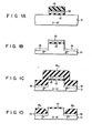
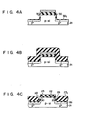
- a conventional liftoff technique will be briefly described with reference to Figs. 1(A) to l(G).
- a thermal oxide film 12 is formed on a silicon substrate 11, and an Al film 13 is formed thereon.
- a photoresist film 14 is formed on the Al film 13 by photoetching.
- the thermal oxide film 12 and the Al film 13 are etched using the photoresist film 14 as a mask.
- the silicon substrate 11 is selectively etched by reactive ion etching (RIE) using the Al film 13 as a mask, thus forming a groove of a depth corresponding to the thickness of a prospective field insulating film, as shown in Fig. l(B).
- RIE reactive ion etching
- a p-type impurity such as boron is ion-implanted in the exposed portion of the silicon substrate 11, thereby forming a p +- type inversion preventive layer (field stopper) 15.
- the impurity has the same conductivity type as that of the silicon substrate but has a higher concentration.
- a thick plasma CVD-SiO 2 film 16 1 is formed to cover the entire surface to a thickness greater than the depth of the groove.
- the CVD-SiO 2 film 16 1 is then etched by an aqueous solution of ammonium fluoride for one minute.
- a film portion of the CVD-SiO 2 film 16 1 which is formed on the side wall of the element formation region is etched faster than the remaining portion of the CVD-SiO 2 film 16 1 . Therefore, the SiO 2 film on the side wall is selectively etched, so that a narrow groove is formed.
- the Al film 13 is removed to lift off the CVD-SiO 2 film portion thereon, thus obtaining a structure as shown in Fig. 1(D).
- a CVD-Si0 2 film 16 2 is formed to cover the entire surface including the narrow groove.
- a photoresist film 17 is then applied to the entire surface so as to obtain a flat surface. It should be noted that the photoresist film is flowable and has the same etching rate as that of the CVD-Si0 2 films 16 1 and 16 2 .
- the photoresist film 17 and the CVD-SiO 2 films 16 1 and 16 2 are then uniformly etched to expose the element formation region.
- Fig. 1(G) shows a structure wherein a gate electrode 19 is formed through a gate oxide film 18 in the element formation region.
- the size of the element formation region is defined by the size of a photoetched mask which is used for etching the silicon substrate 11 by reactive ion etching. Therefore, a dimensional error of the element formation region can be substantially eliminated. Furthermore, the field oxide film has a flat surface, thereby greatly improving lithographic precision and allowing good step coverage of the wiring layer.
- a method for manufacturing a semiconductor device wherein a thickness of an insulating film at a peripheral portion of an element formation region is controlled, having a first step of forming a field insulating film in a groove so as to have a flat surface after an antietching mask is formed on said semiconductor substrate excluding a prospective field region and after said prospective field region is etched to form said groove, and a second step of forming a desired element in said element formation region isolated by said field insulating film, characterized in that the first step comprises the steps of:
- the antioxidant film is formed under the antietching mask.
- a field insulating film is selectively deposited in the groove to obtain a flat surface in the same manner as in the conventional method.
- the exposed portion of the semiconductor substrate is exposed in an oxygen atmosphere using the antioxidant film, thereby oxidizing a portion around the element formation region.
- the oxide film slightly undercuts below the peripheral portion of the element formation region. After an oxide film is formed in the element formation region, the oxide film portion at the peripheral portion of the element formation region becomes thicker than that at the central portion thereof.
- the peripheral portion of the gate oxide film is thick and the central portion is thin along the gate width thereof.
- the potential at the peripheral portion of the element formation region is substantially the same as that at the central portion thereof.
- the threshold voltage of the MOS transistor cannot be decreased.
- carriers will not be concentrated at the peripheral portion of the element formation region, thereby improving the reliability of the device.
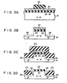
- FIGS. 2 (A) to 2(H) are sectional views for explaining the steps of manufacturing this MOS device.
- a p-type silicon substrate 21 which'has a plane (100) and a resistivity of 5 to 50 ⁇ cm is prepared.
- a thermal oxide film 22 is formed on the p-type silicon substrate 21 to a thickness of 0 about 300 A.
- a silicon nitride film 23 as an antioxidant film is then formed on the thermal oxide film 22 to a thickness of about 1,000 A.
- An At film 24 as an antietching mask and a liftoff material is formed on the silicon nitride film 23.
- a photoresist pattern 25 is formed on the Al film 24 by photoetching so as to correspond to a prospective element formation region. As shown in Fig.
- the At film 24, the silicon nitride film 23 and the oxide film 22 are sequentially etched using the photoresist pattern 25 as a mask. Thereafter, the exposed portion of the silicon substrate 21 is etched by reactive ion etching using CF 4 gas as an etchant, thus forming a groove. Thereafter, an impurity is ion-implanted in the groove, forming a field stopper (guard ring) 26.' As shown in Fig. 2(C), a CVD-SiO 2 film 27 1 as a first insulating film is deposited to cover the entire surface to a thickness slightly greater than the depth of the groove.
- a stepped portion is then selectively etched by ammonium fluoride, and the SiO 2 film 27 1 , together with the At film 24, is lifted off by diluted hydrofluoric acid.
- Fig. 2(D) a structure is obtained wherein the CVD-SiO 2 film 27 1 is selectively left in the groove of the field region, thereby forming a narrow groove 28 therein.
- Fig. 2(E) a CVD-Si0 2 film 27 2 as a second insulating film is deposited to cover the entire surface including the narrow groove 28.
- a flowable photoresist film 29 is formed on the CVD-Si0 2 film 27 2 so as to obtain a flat surface.
- the flowable photoresist film 29 and the CVD-SiO 2 film 27 are uniformly etched by reactive ion etching so as to leave a flat CVD-SiO 2 film 27 only in the field region, as shown in Fig. 2(F). Then, the obtained structure is annealed in a steam atmosphere at 1,000°C for 30 minutes. A thermal oxide film 30 slightly undercuts below the silicon nitride film 23, as shown in Fig. 2(G). The silicon nitride film 23 is removed, and then the underlying thermal oxide film 22 is removed. Thereafter, a gate oxide film 31 is formed, and a gate electrode 32 is formed thereon, as shown in Fig. 2(H).
- the peripheral portion of the thermal oxide film in the element formation region has a thickness greater than the central portion thereof, by about 0.1 and 0.2 ⁇ m, as shown in Fig. 2(H). Therefore, the potential at the peripheral portion of the element formation region under the gate oxide film is substantially the same as that at the central portion thereof. Even if the resultant transistor has a micropattern, its threshold voltage will not be decreased. For example, as shown in Fig. 5, a "hump" bl is formed in a dotted curve b indicating the relationship between the drain current and gate voltage of the MOS transistor manufactured by the conventional method with reference to Figs. 1(A) to l(G). However, according to the method of the present invention with reference to Figs.
- the problem of the conventional method is eliminated as indicated by a solid curve a. Furthermore, the gate oxide film formed by the conventional method tends to break down due to carrier concentration at the peripheral portion along the width of the gate. However, according to the present invention, such a drawback is substantially eliminated, thereby greatly improving the yield of the semiconductor devices.
- the obtained structure is then exposed in an oxygen atmosphere, thereby forming the thermal oxide film 30 such that the peripheral portion of the thermal oxide film 22 together with the thermal oxide film 30 is thicker than the central portion thereof.
- this thermal oxide film 30 may also be formed either before or during deposition of the CVD-Si0 2 film 27 on the field region.
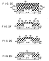
- a thermal oxide film 30 may be formed as shown in Fig. 3(A).
- the silicon nitride film 23 as the antioxidant film is removed, and a CVD-Si0 2 film 27 2 and a flowable photoresist film 29 are formed on the structure shown in Fig. 3(A) so as to obtain a flat surface.
- the flowable photoresist film 29 and the CVD-Si0 2 film 27 2 are uniformly etched, as shown in Fig. 3(C).
- a thermal oxide film 22 is removed and a gate oxide film 31 is formed.
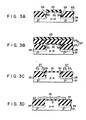
- the resultant structure is then exposed in an oxygen atmosphere in the same manner as in the previous embodiments, thereby forming a thick oxide film 30 1 on the exposed surface of the silicon substrate 21, as shown in Fig. 4(A).
- a thermal oxide film 30 is also formed at the peripheral portion of the element formation region.
- An Al film 24 as a liftoff material must be properly selected in consideration of a temperature of thermal oxidation.
- a CVD-Si0 2 film 27 1 as the first insulating film is deposited to cover the entire surface in the same manner as shown in Fig. 2(C).
- the CVD-Si0 2 film 27 1 is selectively left in the groove of the field region, thereby obtaining a narrow groove 28, as shown in Fig. 4(C).
- a CVD-SiO 2 film 27 2 as the second insulating film is deposited to cover the entire surface, and a flowable photoresist film 29 is applied to obtain a flat surface.
- the flowable photoresist film 29 and the CVD-SiO 2 film 27 (27 1 and 27 2 ) are uniformly etched by reactive ion etching so as to leave a flat SiO 2 film 27 only in the field region, as shown in Fig. 4(E).
- the thermal oxide film 22 is removed, and a gate oxide film and a gate electrode are sequentially deposited thereon.
- a gate oxide film and a gate electrode are sequentially deposited thereon.
- the present invention is applied to an MOS device. However, the present invention may also be applied to element isolation of a bipolar semiconductor device.
Landscapes
- Element Separation (AREA)
- Local Oxidation Of Silicon (AREA)
Applications Claiming Priority (2)
| Application Number | Priority Date | Filing Date | Title |
|---|---|---|---|
| JP57085726A JPS58202545A (ja) | 1982-05-21 | 1982-05-21 | 半導体装置の製造方法 |
| JP85726/82 | 1982-05-21 |
Publications (3)
| Publication Number | Publication Date |
|---|---|
| EP0095328A2 true EP0095328A2 (de) | 1983-11-30 |
| EP0095328A3 EP0095328A3 (en) | 1986-08-20 |
| EP0095328B1 EP0095328B1 (de) | 1989-09-27 |
Family
ID=13866845
Family Applications (1)
| Application Number | Title | Priority Date | Filing Date |
|---|---|---|---|
| EP83302856A Expired EP0095328B1 (de) | 1982-05-21 | 1983-05-19 | Verfahren zum Herstellen einer Halbleiteranordnung durch Kontrollieren der Dicke der Isolierschicht am peripherischen Teil des Elementes |
Country Status (4)
| Country | Link |
|---|---|
| US (1) | US4497108A (de) |
| EP (1) | EP0095328B1 (de) |
| JP (1) | JPS58202545A (de) |
| DE (1) | DE3380652D1 (de) |
Cited By (4)
| Publication number | Priority date | Publication date | Assignee | Title |
|---|---|---|---|---|
| WO1989001702A1 (en) * | 1987-08-17 | 1989-02-23 | Plessey Overseas Limited | A local oxidation of silicon process |
| FR2620861A1 (fr) * | 1987-09-22 | 1989-03-24 | Schiltz Andre | Procede de realisation d'isolement lateral a structure plane |
| EP0309788A1 (de) * | 1987-09-30 | 1989-04-05 | Siemens Aktiengesellschaft | Verfahren zur Erzeugung eines versenkten Oxids |
| US4909897A (en) * | 1986-06-17 | 1990-03-20 | Plessey Overseas Limited | Local oxidation of silicon process |
Families Citing this family (9)
| Publication number | Priority date | Publication date | Assignee | Title |
|---|---|---|---|---|
| US4615746A (en) * | 1983-09-29 | 1986-10-07 | Kenji Kawakita | Method of forming isolated island regions in a semiconductor substrate by selective etching and oxidation and devices formed therefrom |
| US4603468A (en) * | 1984-09-28 | 1986-08-05 | Texas Instruments Incorporated | Method for source/drain self-alignment in stacked CMOS |
| US4972251A (en) * | 1985-08-14 | 1990-11-20 | Fairchild Camera And Instrument Corp. | Multilayer glass passivation structure and method for forming the same |
| JP2742432B2 (ja) * | 1988-11-25 | 1998-04-22 | 株式会社日立製作所 | 半導体装置の製造方法 |
| US5387540A (en) * | 1993-09-30 | 1995-02-07 | Motorola Inc. | Method of forming trench isolation structure in an integrated circuit |
| US6097072A (en) * | 1996-03-28 | 2000-08-01 | Advanced Micro Devices | Trench isolation with suppressed parasitic edge transistors |
| US5721448A (en) * | 1996-07-30 | 1998-02-24 | International Business Machines Corporation | Integrated circuit chip having isolation trenches composed of a dielectric layer with oxidation catalyst material |
| KR100226736B1 (ko) * | 1996-11-07 | 1999-10-15 | 구본준 | 격리영역 형성방법 |
| TW580581B (en) * | 1998-11-10 | 2004-03-21 | Mosel Vitelic Inc | Method of estimating thin-film thickness and formation conditions |
Family Cites Families (5)
| Publication number | Priority date | Publication date | Assignee | Title |
|---|---|---|---|---|
| US4104086A (en) * | 1977-08-15 | 1978-08-01 | International Business Machines Corporation | Method for forming isolated regions of silicon utilizing reactive ion etching |
| JPS55153342A (en) * | 1979-05-18 | 1980-11-29 | Fujitsu Ltd | Semiconductor device and its manufacture |
| JPS56138938A (en) * | 1980-03-31 | 1981-10-29 | Chiyou Lsi Gijutsu Kenkyu Kumiai | Manufacture of semiconductor device |
| DE3170644D1 (en) * | 1980-11-29 | 1985-06-27 | Toshiba Kk | Method of filling a groove in a semiconductor substrate |
| US4407851A (en) * | 1981-04-13 | 1983-10-04 | Tokyo Shibaura Denki Kabushiki Kaisha | Method for manufacturing semiconductor device |
-
1982
- 1982-05-21 JP JP57085726A patent/JPS58202545A/ja active Granted
-
1983
- 1983-05-17 US US06/495,483 patent/US4497108A/en not_active Expired - Lifetime
- 1983-05-19 DE DE8383302856T patent/DE3380652D1/de not_active Expired
- 1983-05-19 EP EP83302856A patent/EP0095328B1/de not_active Expired
Cited By (4)
| Publication number | Priority date | Publication date | Assignee | Title |
|---|---|---|---|---|
| US4909897A (en) * | 1986-06-17 | 1990-03-20 | Plessey Overseas Limited | Local oxidation of silicon process |
| WO1989001702A1 (en) * | 1987-08-17 | 1989-02-23 | Plessey Overseas Limited | A local oxidation of silicon process |
| FR2620861A1 (fr) * | 1987-09-22 | 1989-03-24 | Schiltz Andre | Procede de realisation d'isolement lateral a structure plane |
| EP0309788A1 (de) * | 1987-09-30 | 1989-04-05 | Siemens Aktiengesellschaft | Verfahren zur Erzeugung eines versenkten Oxids |
Also Published As
| Publication number | Publication date |
|---|---|
| US4497108A (en) | 1985-02-05 |
| JPH0427702B2 (de) | 1992-05-12 |
| DE3380652D1 (en) | 1989-11-02 |
| JPS58202545A (ja) | 1983-11-25 |
| EP0095328B1 (de) | 1989-09-27 |
| EP0095328A3 (en) | 1986-08-20 |
Similar Documents
| Publication | Publication Date | Title |
|---|---|---|
| US3961999A (en) | Method for forming recessed dielectric isolation with a minimized "bird's beak" problem | |
| EP0152615B1 (de) | Schottky-Feldeffekttransistor und Verfahren zu dessen Herstellung | |
| US4546538A (en) | Method of manufacturing semiconductor integrated circuit devices having dielectric isolation regions | |
| EP0107416B1 (de) | Verfahren zur Herstellung einer Halbleiteranordnung | |
| US3966514A (en) | Method for forming dielectric isolation combining dielectric deposition and thermal oxidation | |
| JPH0329172B2 (de) | ||
| EP0055521A1 (de) | Verfahren zum Füllen einer Rille in einem Halbleitersubstrat | |
| US4044454A (en) | Method for forming integrated circuit regions defined by recessed dielectric isolation | |
| US4497108A (en) | Method for manufacturing semiconductor device by controlling thickness of insulating film at peripheral portion of element formation region | |
| EP0178000B1 (de) | Verfahren zur Herstellung submikronischer Gräben, z.B. in Halbleitermaterial und nach diesem Verfahren hergestellte Anordnungen | |
| EP0180256A1 (de) | Verfahren zum Herstellen von Kontakten auf einer Halbleitervorrichtung | |
| KR960001175B1 (ko) | 반도체장치의 제조방법 | |
| EP0050973B1 (de) | Verfahren zur Maskierung von Halbleiteranordnungen unter Verwendung einer Polymerschicht | |
| US4810668A (en) | Semiconductor device element-isolation by oxidation of polysilicon in trench | |
| JPS6123657B2 (de) | ||
| US4885261A (en) | Method for isolating a semiconductor element | |
| EP0293979A2 (de) | Oxydisolierungsstruktur ohne bird-beak für integrierte Schaltungen | |
| US4504333A (en) | Method of making field oxide regions | |
| US4696095A (en) | Process for isolation using self-aligned diffusion process | |
| JPH0210730A (ja) | 集積回路チップ上の電界効果トランジスタ用のフィールド・アイソレーション形成方法と構造 | |
| US5763316A (en) | Substrate isolation process to minimize junction leakage | |
| JPS5923476B2 (ja) | 半導体装置の製造方法 | |
| JPS5856436A (ja) | 半導体装置の製造方法 | |
| JPH079930B2 (ja) | 半導体装置の製造方法 | |
| KR0135031B1 (ko) | 반도체 소자의 격리방법 |
Legal Events
| Date | Code | Title | Description |
|---|---|---|---|
| PUAI | Public reference made under article 153(3) epc to a published international application that has entered the european phase |
Free format text: ORIGINAL CODE: 0009012 |
|
| 17P | Request for examination filed |
Effective date: 19830527 |
|
| AK | Designated contracting states |
Designated state(s): DE FR GB IT NL |
|
| RAP1 | Party data changed (applicant data changed or rights of an application transferred) |
Owner name: KABUSHIKI KAISHA TOSHIBA |
|
| PUAL | Search report despatched |
Free format text: ORIGINAL CODE: 0009013 |
|
| AK | Designated contracting states |
Kind code of ref document: A3 Designated state(s): DE FR GB IT NL |
|
| 17Q | First examination report despatched |
Effective date: 19880224 |
|
| GRAA | (expected) grant |
Free format text: ORIGINAL CODE: 0009210 |
|
| AK | Designated contracting states |
Kind code of ref document: B1 Designated state(s): DE FR GB IT NL |
|
| ITF | It: translation for a ep patent filed | ||
| REF | Corresponds to: |
Ref document number: 3380652 Country of ref document: DE Date of ref document: 19891102 |
|
| ET | Fr: translation filed | ||
| PLBE | No opposition filed within time limit |
Free format text: ORIGINAL CODE: 0009261 |
|
| 26N | No opposition filed | ||
| ITTA | It: last paid annual fee | ||
| PGFP | Annual fee paid to national office [announced via postgrant information from national office to epo] |
Ref country code: GB Payment date: 19970512 Year of fee payment: 15 |
|
| PGFP | Annual fee paid to national office [announced via postgrant information from national office to epo] |
Ref country code: FR Payment date: 19970513 Year of fee payment: 15 |
|
| PGFP | Annual fee paid to national office [announced via postgrant information from national office to epo] |
Ref country code: DE Payment date: 19970523 Year of fee payment: 15 |
|
| PGFP | Annual fee paid to national office [announced via postgrant information from national office to epo] |
Ref country code: NL Payment date: 19970529 Year of fee payment: 15 |
|
| PG25 | Lapsed in a contracting state [announced via postgrant information from national office to epo] |
Ref country code: GB Free format text: LAPSE BECAUSE OF NON-PAYMENT OF DUE FEES Effective date: 19980519 |
|
| PG25 | Lapsed in a contracting state [announced via postgrant information from national office to epo] |
Ref country code: FR Free format text: LAPSE BECAUSE OF NON-PAYMENT OF DUE FEES Effective date: 19980531 |
|
| PG25 | Lapsed in a contracting state [announced via postgrant information from national office to epo] |
Ref country code: NL Free format text: LAPSE BECAUSE OF NON-PAYMENT OF DUE FEES Effective date: 19981201 |
|
| GBPC | Gb: european patent ceased through non-payment of renewal fee |
Effective date: 19980519 |
|
| NLV4 | Nl: lapsed or anulled due to non-payment of the annual fee |
Effective date: 19981201 |
|
| PG25 | Lapsed in a contracting state [announced via postgrant information from national office to epo] |
Ref country code: DE Free format text: LAPSE BECAUSE OF NON-PAYMENT OF DUE FEES Effective date: 19990302 |
|
| REG | Reference to a national code |
Ref country code: FR Ref legal event code: ST |