EP0067412B1 - Halbleiteranordnung mit Isolationszonen und Verfahren zu dessen Herstellung - Google Patents
Halbleiteranordnung mit Isolationszonen und Verfahren zu dessen Herstellung Download PDFInfo
- Publication number
- EP0067412B1 EP0067412B1 EP82105043A EP82105043A EP0067412B1 EP 0067412 B1 EP0067412 B1 EP 0067412B1 EP 82105043 A EP82105043 A EP 82105043A EP 82105043 A EP82105043 A EP 82105043A EP 0067412 B1 EP0067412 B1 EP 0067412B1
- Authority
- EP
- European Patent Office
- Prior art keywords
- insulating film
- film
- region
- semiconductor device
- forming
- Prior art date
- Legal status (The legal status is an assumption and is not a legal conclusion. Google has not performed a legal analysis and makes no representation as to the accuracy of the status listed.)
- Expired
Links
Images

Classifications
-
- H—ELECTRICITY
- H10—SEMICONDUCTOR DEVICES; ELECTRIC SOLID-STATE DEVICES NOT OTHERWISE PROVIDED FOR
- H10P—GENERIC PROCESSES OR APPARATUS FOR THE MANUFACTURE OR TREATMENT OF DEVICES COVERED BY CLASS H10
- H10P95/00—Generic processes or apparatus for manufacture or treatments not covered by the other groups of this subclass
- H10P95/06—Planarisation of inorganic insulating materials
-
- H—ELECTRICITY
- H10—SEMICONDUCTOR DEVICES; ELECTRIC SOLID-STATE DEVICES NOT OTHERWISE PROVIDED FOR
- H10W—GENERIC PACKAGES, INTERCONNECTIONS, CONNECTORS OR OTHER CONSTRUCTIONAL DETAILS OF DEVICES COVERED BY CLASS H10
- H10W10/00—Isolation regions in semiconductor bodies between components of integrated devices
- H10W10/01—Manufacture or treatment
- H10W10/011—Manufacture or treatment of isolation regions comprising dielectric materials
- H10W10/014—Manufacture or treatment of isolation regions comprising dielectric materials using trench refilling with dielectric materials, e.g. shallow trench isolations
-
- H—ELECTRICITY
- H10—SEMICONDUCTOR DEVICES; ELECTRIC SOLID-STATE DEVICES NOT OTHERWISE PROVIDED FOR
- H10W—GENERIC PACKAGES, INTERCONNECTIONS, CONNECTORS OR OTHER CONSTRUCTIONAL DETAILS OF DEVICES COVERED BY CLASS H10
- H10W10/00—Isolation regions in semiconductor bodies between components of integrated devices
- H10W10/10—Isolation regions comprising dielectric materials
- H10W10/17—Isolation regions comprising dielectric materials formed using trench refilling with dielectric materials, e.g. shallow trench isolations
Definitions
- This invention relates to a semiconductor device in which a comparatively thick insulating film is buried in a field region and also a method of manufacturing such a semiconductor device.
- a thick insulating film is formed in a so-called field region between adjacent elements in order to eliminate defective insulation due to parasitic channel and also reduce the parasitic capacitance.
- the inter-element isolation in such a semiconductor device is attained by a well-known selective oxidation method.
- the element formation region is covered with an oxidizable mask, typically a silicon nitride film, and a thick oxide film is selectively formed over the field region through high temperature oxidation.
- an oxidizable mask typically a silicon nitride film
- a thick oxide film is selectively formed over the field region through high temperature oxidation.
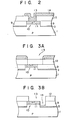
- the field oxide film protrudes in the form of a bird's beak from the end of the silicon nitride film during the high temperature oxidation. This causes dimensional errors of the element formation region and also prevents high density integration of integrated circuits.
- a surface step of about one half of the field oxide film (which is about 0.7 to 1.0 urn) in height is formed in the field region and element formation region after the formation of the field oxide film. This step remains as such in the subsequent steps to reduce the precision of the subsequent lithography. Also the reliability of the metal lead is reduced at the step.
- a BOX (buried oxide) method is also well known as a method which can eliminate the bird's beak and permits a flat buried field oxide film to be obtained.
- a silicon substrate 1 is prepared, and it is selectively etched to a desired depth corresponding to the field film thickness with the element formation region covered with a mask 2 by the ordinary photoetching process.
- an impurity of the same conductivity type as the silicon substrate for the prevention of field inversion for instance boron 3 in case of a P-type substrate, is injected by ion implantation into the field region by using the same mask 2.
- a silicon oxide film 4 to be buried in the field region is formed by using a lift-off process.
- the lift-off process may be carried out as follows. In the first place, a plasma CVD Si0 2 film is deposited over the entire surface of the wafer shown in Fig. 1(B). Then, etching for about one minute is done using, for instance, ammonium fluoride. As a result, a portion of the plasma CVD Si0 2 film deposited on the side surfaces of the raised portion formed at the boundary between the field region and element formation region is selectively removed because the etching speed for this portion is higher than that for the rest of the plasma CVD Si0 2 film formed on the non-raised or flat portion of the wafer by 3 to 20 times.
- a narrow groove 5 having a V-shaped sectional profile is formed at the boundary between the field region and element formation region as shown in Fig. 1(C).
- a CVD Si0 2 film 6 is deposited to fill the narrow groove 5.
- a groove 7 is formed in the CVD Si0 2 film in a portion thereof over the narrow groove 5 mentioned above.
- a film 8 which has fluidity and can be etched at the same rate as the CVD Si0 2 film is formed to fill the groove 7 thereby providing a flat surface.
- the fluid film 8 and CVD SiO z fiim 6 are etched away, and further etching is carried out to expose the silicon in the element formation region.
- a substantially flat field region consisting of the CVD Si0 2 film and plasma CVD Si0 2 film is formed, as shown in Fig. 1(E).
- a desired element is then formed in the element formation region 10 by the ordinary method.
- the dimensions of the element region are defined solely by the dimensions of the mask formed for the photoetching process if reactive ion etching (RIE) which is free from side etching is used for the etching of the silicon substrate.
- RIE reactive ion etching
- the hole 13 may be thought to form the hole 13 such that it partly overlaps the diffusion layer 11 and field region 9 as shown in Fig. 3A. By so doing, the semiconductor device integration density may be promoted.
- part 14 of the field oxide film 9 is also etched away at the time of the hole formation as shown in Fig. 3(B). Therefore, abnormal electric connection of a subsequently formed metal lead and the silicon substrate is liable to result.
- This invention has been made in view of the drawbacks inherent in the prior art inter-element isolation method using oxide film. Its object, accordingly, is to provide a method of manufacturing a semiconductor device, in which an insulating film of a different substance than oxide film is formed along an area neighbouring an element formation region, thus permitting the formation of a hole partly overlapping a field region thereby enabling to increase the semiconductor device integration density.
- a first aspect of the invention lies in providing a semiconductor device of the type in which a field region between adjacent element regions formed in a semiconductor substrate is constituted by a buried first insulating film having the top surface substantially flush with the top surface of the element regions, and a lead layer is electrically connected to each element region by through holes formed in a silicon oxide film formed to cover the element regions and field region, said semiconductor device being characterized in that a second insulating film is disposed around each of the element regions, at a boundary space between the field region and the element region, said second insulating film being consisted of a substance other than silicon oxide having a lower etching rate than silicon oxide, and that said holes are formed to overlap said each element region and said second insulating film.
- a second aspect of the invention lies in providing a method of manufacturing a semiconductor device, which comprises (a) a step of forming a recess in a portion of a semiconductor substrate corresponding to a field region, (b) a step of forming a thick first insulating film consisting of silicon oxide in said recess such that a groove is defined at the edge of said first insulating film, the surface of said thick first insulating film being flush with the surface of the semiconductor substrate, (c) a step of forming a second insulating film over the entire surface to fill said groove, (d) a step of exposing portions of the substrate corresponding to element formation regions while leaving said first and second insulating films in said recess, (e) a step of forming each of said element formation regions with an impurity-doped surface region adjacent to the field region, (f) a step offorming over the entire surface a third insulating film consisting of silicon oxide, and (g) a step of forming through said third insulating film a contact
- the first point is that for burying in an insulating film in the field region by the usual BOX method a first insulating film (for instance a CVD silicon oxide film) is formed by the well-known lift-off process and then a second insulating film of a substance, which has a selecting etching property with respect to a third insulating film which is subsequently formed on the aforementioned first and second insulating films and therefore has substantially a lower etching rate with respect to the third insulating film in a particular etching method, for instance alumina, silicon nitride or tantalum oxide, is formed in a V-shaped groove defined at the boundary defined between the first insulating film and an element formation region formed by the lift-off process.
- a first insulating film for instance a CVD silicon oxide film
- a second insulating film of a substance which has a selecting etching property with respect to a third insulating film which is subsequently formed on the aforementioned first and second insulating films and therefore
- the second point is that it has been made possible to obtain an electric connection between the impurity-doped layer in the element formation region and a lead through a contact hole which is formed in the third insulating film in such a manner that the hole partly overlaps the second insulating film in the field region, thus alleviating restrictions on the dimensions of the hole.
- the element formation region is thus surrounded by the second insulating film which has a lower etching rate than the third insulating film.
- the etching can be stopped at the surface of the second insulating film in the field region. That is, it is possible to avoid overetching of the field oxide film as shown in Fig. 3(B), thus eliminating abnormal electric connection between a subsequently formed lead and substrate, thereby increasing the reliability of the electric connection between diffusion layer and lead substance in the hole.
- the presence of the second insulating film makes it possible to use of a different insulating film from that of the conventional oxide film as a gate insulating film that is provided underneath a gate electrode of a semiconductor device, for instance alumina film, silicon nitride film or tantalum oxide film.
- the gate insulating film may be made of the same substance as the second insulating film formed in a portion of the field region adjacent to the element formation region, so that it is possible to prevent charge trap in the junction between these two layers.
- a P type substrate is used as the silicon substrate
- an alumina film as the second insulating film adjacent to the element formation region
- the inversion of the silicon substrate at the interface between the alumina film and silicon substrate can be prevented, because the alumina film has a characteristic of being negatively charged.
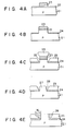
- a P-type silicon substrate 21 of surface orientation (100) and having a resistivity of 5 to 50 ⁇ ⁇ cm is prepared, and a thermal oxide film 22 is formed thereon to a thickness of about 500 A.
- a resist film 23 is formed to cover the element formation region by the ordinary photoetching process.
- a portion of the silicon substrate constituting a field region is etched to a depth of, for instance 0.6 pm with the resist film 23 as a mask. Then, boron for field inversion prevention is ion-implanted into silicon in the field region by using the same mask, thus forming a P +- type layer 24.
- a plasma CVD Si0 2 film is deposited over the entire surface of the wafer, and side portions formed at the boundary between the field region and element formation region is selectively removed by the lift-off process using, for instance, ammonium fluoride.
- the resist film 23 is then etched away together with the plasma CVD Si0 2 film thereon as shown in Fig. 4(D), leaving the plasma CVD Si0 2 film as a first insulating film 25 in the field region with a V-shaped groove 28 defined at the perimeter thereof.
- a second insulating film of a substance other than the first insulating film, for instance an alumina film is uniformly deposited.
- a substance for providing a flat surface typically a resist film (not shown), is then coated on the surface.
- the resist film and alumina film are uniformly etched away, whereby a flat field region including the second insulating film 26 filling the groove 28 is obtained as shown in Fig. 4(E).
- a diffusion layer 29 of a given type for instance N +- type
- a resist pattern 31 is formed on the insulating film 30, and with thus pattern as a mask a hole (i.e., contact hole) 32 is formed in the film 30 by reactive ion etching using, for instance, a mixture gas containing CF 4 (or C 3 F $ ) gas and H 2 gas.
- the hole 32 is formed to partly overlap the diffusion layer 29 and second insulating film 26.
- the etching can be stopped at the surface of the second insulating film 26 because the etching rate of the insulating film 26 is substantially lower as compared to the third insulating film 30.
- the field insulating film is not etched during the formation of the hole 32 which partly overlaps the field region.
- the possibility of electric connection between metal lead and substrate as mentioned before, is thus eliminated, and the reliability of the electric connection between the electrode lead and diffusion layer in the hole can be extremely increased.
- the width W 1 of the surface of the second insulating film 26 can be made substantially equal to the thickness of the first insulating layer.
- the width W 2 of the hole can be given an increased margin of 2XW, at the most as compared to the prior art case described earlier in connection with Fig. 2.
- the precision required for the mask register for forming the hole 32 can thus be extremely alleviated compared to the prior art. It is thus possible to improve the semiconductor device integration density without spoiling the features of the conventional BOX method.
- the P +- type layer 24 for inversion prevention may be omitted in some case.
- the second insulating film 26 is an alumina film
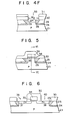
- Figs. 5 and 6 illustrate advantages of the invention in case where a gate insulating film 35 which is provided underneath a gate electrode 34 of a MOS device is made of a different insulating film from the prior art silicon oxide film, for instance a silicon nitride film, an alumina film or a tantalum oxide film.
- the second insulating film 26 is formed by using the same substance as the gate insulating film 35. Since in this case the gate insulating film 36 and second insulating film 25 defining a junction 36 between them are made of the same substance, there is no possibility of charge trap at the junction 36, which is very desirable from ths standpoint of the characteristics of the element.
- Fig. 6 is a section taken along line VI-VI in Fig. 5. As is shown, holes 39 and 40 for source 37 and drain 38 may also be formed to partly overlap the second insulating film 26.
- the other reference numerals designate like parts as in Fig. 4(F).
- the invention is naturally applicable for interelement isolation not only for a MOS device but also for a bipolar semiconductor device.
Landscapes
- Element Separation (AREA)
- Local Oxidation Of Silicon (AREA)
- Drying Of Semiconductors (AREA)
Claims (7)
dadurch gekennzeichnet, daß der dritte Isolierfilm (30) nach Schritt (f) aus einer Substanz besteht, die eine höhere Ätzgeschwindigkeit als der zweite Isolierfilm (26) aufweist, und daß das Kontaktloch den zweiten (lsolier-)Film (26) in der Ausnehmung überlappt und der zweite Isolierfilm (26) aus einer von Siliziumoxidfilm verschiedenen Substanz geformt ist.
Applications Claiming Priority (2)
| Application Number | Priority Date | Filing Date | Title |
|---|---|---|---|
| JP56088256A JPS57204148A (en) | 1981-06-10 | 1981-06-10 | Manufacture of semiconductor device |
| JP88256/81 | 1981-06-10 |
Publications (3)
| Publication Number | Publication Date |
|---|---|
| EP0067412A2 EP0067412A2 (de) | 1982-12-22 |
| EP0067412A3 EP0067412A3 (en) | 1986-07-09 |
| EP0067412B1 true EP0067412B1 (de) | 1989-04-19 |
Family
ID=13937786
Family Applications (1)
| Application Number | Title | Priority Date | Filing Date |
|---|---|---|---|
| EP82105043A Expired EP0067412B1 (de) | 1981-06-10 | 1982-06-08 | Halbleiteranordnung mit Isolationszonen und Verfahren zu dessen Herstellung |
Country Status (4)
| Country | Link |
|---|---|
| US (1) | US4504333A (de) |
| EP (1) | EP0067412B1 (de) |
| JP (1) | JPS57204148A (de) |
| DE (1) | DE3279632D1 (de) |
Families Citing this family (7)
| Publication number | Priority date | Publication date | Assignee | Title |
|---|---|---|---|---|
| EP0126292B1 (de) * | 1983-04-21 | 1987-12-02 | Kabushiki Kaisha Toshiba | Halbleitervorrichtung mit einer Schicht zur Isolation der Elemente und Verfahren zu ihrer Herstellung |
| US4729006A (en) * | 1986-03-17 | 1988-03-01 | International Business Machines Corporation | Sidewall spacers for CMOS circuit stress relief/isolation and method for making |
| US4996165A (en) * | 1989-04-21 | 1991-02-26 | Rockwell International Corporation | Self-aligned dielectric assisted planarization process |
| EP0607658A3 (de) * | 1992-11-13 | 1995-08-30 | At & T Corp | MOSFET-Herstellung. |
| JPH09312391A (ja) * | 1996-05-22 | 1997-12-02 | Toshiba Corp | 半導体装置およびその製造方法 |
| TW497120B (en) * | 2000-03-06 | 2002-08-01 | Toshiba Corp | Transistor, semiconductor device and manufacturing method of semiconductor device |
| US6348394B1 (en) | 2000-05-18 | 2002-02-19 | International Business Machines Corporation | Method and device for array threshold voltage control by trapped charge in trench isolation |
Family Cites Families (7)
| Publication number | Priority date | Publication date | Assignee | Title |
|---|---|---|---|---|
| US3646665A (en) * | 1970-05-22 | 1972-03-07 | Gen Electric | Complementary mis-fet devices and method of fabrication |
| US3766637A (en) * | 1972-05-04 | 1973-10-23 | Rca Corp | Method of making mos transistors |
| US4335391A (en) * | 1978-12-11 | 1982-06-15 | Texas Instruments Incorporated | Non-volatile semiconductor memory elements and methods of making |
| US4222792A (en) * | 1979-09-10 | 1980-09-16 | International Business Machines Corporation | Planar deep oxide isolation process utilizing resin glass and E-beam exposure |
| US4252582A (en) * | 1980-01-25 | 1981-02-24 | International Business Machines Corporation | Self aligned method for making bipolar transistor having minimum base to emitter contact spacing |
| DE3170644D1 (en) * | 1980-11-29 | 1985-06-27 | Toshiba Kk | Method of filling a groove in a semiconductor substrate |
| US4407851A (en) * | 1981-04-13 | 1983-10-04 | Tokyo Shibaura Denki Kabushiki Kaisha | Method for manufacturing semiconductor device |
-
1981
- 1981-06-10 JP JP56088256A patent/JPS57204148A/ja active Pending
-
1982
- 1982-06-04 US US06/384,946 patent/US4504333A/en not_active Expired - Lifetime
- 1982-06-08 DE DE8282105043T patent/DE3279632D1/de not_active Expired
- 1982-06-08 EP EP82105043A patent/EP0067412B1/de not_active Expired
Also Published As
| Publication number | Publication date |
|---|---|
| DE3279632D1 (en) | 1989-05-24 |
| US4504333A (en) | 1985-03-12 |
| EP0067412A2 (de) | 1982-12-22 |
| JPS57204148A (en) | 1982-12-14 |
| EP0067412A3 (en) | 1986-07-09 |
Similar Documents
| Publication | Publication Date | Title |
|---|---|---|
| EP0074541B1 (de) | Verfahren zur Herstellung einer Halbleiteranordnung mit dielektrischen Isolationszonen | |
| EP0660389B1 (de) | Verfahren zur Herstellung von Halbleiteranordnungen mit Isolationszonen | |
| JP2505961B2 (ja) | 半導体構造用のスタッドを形成する方法および半導体デバイス | |
| US4073054A (en) | Method of fabricating semiconductor device | |
| KR100190105B1 (ko) | 게이트전극의 제조방법 및 그에 따라 제조된 게이트구조 | |
| US4689872A (en) | Method of manufacturing a semiconductor device | |
| US4660068A (en) | Substrate structure of semiconductor device and method of manufacturing the same | |
| JP3793626B2 (ja) | 自己整合接点をもつトランジスタの製造方法 | |
| JPH10335441A (ja) | 半導体装置の製造方法 | |
| KR950012918B1 (ko) | 선택적 텅스텐 박막의 2단계 퇴적에 의한 콘택 매립방법 | |
| US5231046A (en) | Method for fabricating an interconnection pattern on a BPSG-filled trench isolation structure | |
| EP0067412B1 (de) | Halbleiteranordnung mit Isolationszonen und Verfahren zu dessen Herstellung | |
| KR100537812B1 (ko) | 이중 필드 분리 구조의 형성 방법 | |
| EP0095328B1 (de) | Verfahren zum Herstellen einer Halbleiteranordnung durch Kontrollieren der Dicke der Isolierschicht am peripherischen Teil des Elementes | |
| KR880000975B1 (ko) | 반도체 장치의 기판구조 및 그 제조방법 | |
| US4885261A (en) | Method for isolating a semiconductor element | |
| JPH05849B2 (de) | ||
| KR19980068057A (ko) | 트렌치 소자분리방법 | |
| US20010026995A1 (en) | Method of forming shallow trench isolation | |
| JPH0426162A (ja) | 浮遊ゲート型半導体記憶装置およびその製造方法 | |
| US6537899B2 (en) | Semiconductor device and a method of fabricating the same | |
| KR100191710B1 (ko) | 반도체 소자의 금속 배선 방법 | |
| US6716720B2 (en) | Method for filling depressions on a semiconductor wafer | |
| JPH0461346A (ja) | バイポーラ型半導体集積回路装置の製造方法 | |
| JP2855981B2 (ja) | 半導体装置の製造方法 |
Legal Events
| Date | Code | Title | Description |
|---|---|---|---|
| PUAI | Public reference made under article 153(3) epc to a published international application that has entered the european phase |
Free format text: ORIGINAL CODE: 0009012 |
|
| 17P | Request for examination filed |
Effective date: 19820705 |
|
| AK | Designated contracting states |
Designated state(s): DE FR GB IT |
|
| RAP1 | Party data changed (applicant data changed or rights of an application transferred) |
Owner name: KABUSHIKI KAISHA TOSHIBA |
|
| PUAL | Search report despatched |
Free format text: ORIGINAL CODE: 0009013 |
|
| AK | Designated contracting states |
Kind code of ref document: A3 Designated state(s): DE FR GB IT |
|
| 17Q | First examination report despatched |
Effective date: 19871111 |
|
| RBV | Designated contracting states (corrected) |
Designated state(s): DE FR GB |
|
| GRAA | (expected) grant |
Free format text: ORIGINAL CODE: 0009210 |
|
| AK | Designated contracting states |
Kind code of ref document: B1 Designated state(s): DE FR GB |
|
| REF | Corresponds to: |
Ref document number: 3279632 Country of ref document: DE Date of ref document: 19890524 |
|
| ET | Fr: translation filed | ||
| PLBE | No opposition filed within time limit |
Free format text: ORIGINAL CODE: 0009261 |
|
| STAA | Information on the status of an ep patent application or granted ep patent |
Free format text: STATUS: NO OPPOSITION FILED WITHIN TIME LIMIT |
|
| 26N | No opposition filed | ||
| PGFP | Annual fee paid to national office [announced via postgrant information from national office to epo] |
Ref country code: GB Payment date: 19930528 Year of fee payment: 12 |
|
| PGFP | Annual fee paid to national office [announced via postgrant information from national office to epo] |
Ref country code: FR Payment date: 19930609 Year of fee payment: 12 |
|
| PGFP | Annual fee paid to national office [announced via postgrant information from national office to epo] |
Ref country code: DE Payment date: 19930623 Year of fee payment: 12 |
|
| PG25 | Lapsed in a contracting state [announced via postgrant information from national office to epo] |
Ref country code: GB Effective date: 19940608 |
|
| GBPC | Gb: european patent ceased through non-payment of renewal fee |
Effective date: 19940608 |
|
| PG25 | Lapsed in a contracting state [announced via postgrant information from national office to epo] |
Ref country code: FR Effective date: 19950228 |
|
| PG25 | Lapsed in a contracting state [announced via postgrant information from national office to epo] |
Ref country code: DE Effective date: 19950301 |
|
| REG | Reference to a national code |
Ref country code: FR Ref legal event code: ST |