EP0086907B1 - Recording apparatus - Google Patents
Recording apparatus Download PDFInfo
- Publication number
- EP0086907B1 EP0086907B1 EP82201324A EP82201324A EP0086907B1 EP 0086907 B1 EP0086907 B1 EP 0086907B1 EP 82201324 A EP82201324 A EP 82201324A EP 82201324 A EP82201324 A EP 82201324A EP 0086907 B1 EP0086907 B1 EP 0086907B1
- Authority
- EP
- European Patent Office
- Prior art keywords
- chip
- row
- radiation sources
- rows
- led
- Prior art date
- Legal status (The legal status is an assumption and is not a legal conclusion. Google has not performed a legal analysis and makes no representation as to the accuracy of the status listed.)
- Expired
Links
Images




Classifications
-
- H—ELECTRICITY
- H04—ELECTRIC COMMUNICATION TECHNIQUE
- H04N—PICTORIAL COMMUNICATION, e.g. TELEVISION
- H04N1/00—Scanning, transmission or reproduction of documents or the like, e.g. facsimile transmission; Details thereof
- H04N1/04—Scanning arrangements, i.e. arrangements for the displacement of active reading or reproducing elements relative to the original or reproducing medium, or vice versa
- H04N1/19—Scanning arrangements, i.e. arrangements for the displacement of active reading or reproducing elements relative to the original or reproducing medium, or vice versa using multi-element arrays
- H04N1/195—Scanning arrangements, i.e. arrangements for the displacement of active reading or reproducing elements relative to the original or reproducing medium, or vice versa using multi-element arrays the array comprising a two-dimensional [2D] array
- H04N1/19505—Scanning picture elements spaced apart from one another in at least one direction
- H04N1/19515—Scanning picture elements spaced apart from one another in at least one direction in two directions
-
- B—PERFORMING OPERATIONS; TRANSPORTING
- B41—PRINTING; LINING MACHINES; TYPEWRITERS; STAMPS
- B41J—TYPEWRITERS; SELECTIVE PRINTING MECHANISMS, i.e. MECHANISMS PRINTING OTHERWISE THAN FROM A FORME; CORRECTION OF TYPOGRAPHICAL ERRORS
- B41J2/00—Typewriters or selective printing mechanisms characterised by the printing or marking process for which they are designed
- B41J2/435—Typewriters or selective printing mechanisms characterised by the printing or marking process for which they are designed characterised by selective application of radiation to a printing material or impression-transfer material
- B41J2/447—Typewriters or selective printing mechanisms characterised by the printing or marking process for which they are designed characterised by selective application of radiation to a printing material or impression-transfer material using arrays of radiation sources
- B41J2/45—Typewriters or selective printing mechanisms characterised by the printing or marking process for which they are designed characterised by selective application of radiation to a printing material or impression-transfer material using arrays of radiation sources using light-emitting diode [LED] or laser arrays
- B41J2/451—Special optical means therefor, e.g. lenses, mirrors, focusing means
-
- G—PHYSICS
- G06—COMPUTING OR CALCULATING; COUNTING
- G06K—GRAPHICAL DATA READING; PRESENTATION OF DATA; RECORD CARRIERS; HANDLING RECORD CARRIERS
- G06K15/00—Arrangements for producing a permanent visual presentation of the output data, e.g. computer output printers
- G06K15/02—Arrangements for producing a permanent visual presentation of the output data, e.g. computer output printers using printers
- G06K15/12—Arrangements for producing a permanent visual presentation of the output data, e.g. computer output printers using printers by photographic printing, e.g. by laser printers
- G06K15/1238—Arrangements for producing a permanent visual presentation of the output data, e.g. computer output printers using printers by photographic printing, e.g. by laser printers simultaneously exposing more than one point
- G06K15/1242—Arrangements for producing a permanent visual presentation of the output data, e.g. computer output printers using printers by photographic printing, e.g. by laser printers simultaneously exposing more than one point on one main scanning line
- G06K15/1247—Arrangements for producing a permanent visual presentation of the output data, e.g. computer output printers using printers by photographic printing, e.g. by laser printers simultaneously exposing more than one point on one main scanning line using an array of light sources, e.g. a linear array
-
- H—ELECTRICITY
- H04—ELECTRIC COMMUNICATION TECHNIQUE
- H04N—PICTORIAL COMMUNICATION, e.g. TELEVISION
- H04N1/00—Scanning, transmission or reproduction of documents or the like, e.g. facsimile transmission; Details thereof
- H04N1/024—Details of scanning heads ; Means for illuminating the original
- H04N1/032—Details of scanning heads ; Means for illuminating the original for picture information reproduction
- H04N1/036—Details of scanning heads ; Means for illuminating the original for picture information reproduction for optical reproduction
-
- H—ELECTRICITY
- H04—ELECTRIC COMMUNICATION TECHNIQUE
- H04N—PICTORIAL COMMUNICATION, e.g. TELEVISION
- H04N1/00—Scanning, transmission or reproduction of documents or the like, e.g. facsimile transmission; Details thereof
- H04N1/04—Scanning arrangements, i.e. arrangements for the displacement of active reading or reproducing elements relative to the original or reproducing medium, or vice versa
- H04N1/19—Scanning arrangements, i.e. arrangements for the displacement of active reading or reproducing elements relative to the original or reproducing medium, or vice versa using multi-element arrays
- H04N1/195—Scanning arrangements, i.e. arrangements for the displacement of active reading or reproducing elements relative to the original or reproducing medium, or vice versa using multi-element arrays the array comprising a two-dimensional [2D] array
- H04N1/19505—Scanning picture elements spaced apart from one another in at least one direction
-
- H—ELECTRICITY
- H04—ELECTRIC COMMUNICATION TECHNIQUE
- H04N—PICTORIAL COMMUNICATION, e.g. TELEVISION
- H04N1/00—Scanning, transmission or reproduction of documents or the like, e.g. facsimile transmission; Details thereof
- H04N1/04—Scanning arrangements, i.e. arrangements for the displacement of active reading or reproducing elements relative to the original or reproducing medium, or vice versa
- H04N1/19—Scanning arrangements, i.e. arrangements for the displacement of active reading or reproducing elements relative to the original or reproducing medium, or vice versa using multi-element arrays
- H04N1/195—Scanning arrangements, i.e. arrangements for the displacement of active reading or reproducing elements relative to the original or reproducing medium, or vice versa using multi-element arrays the array comprising a two-dimensional [2D] array
- H04N1/19505—Scanning picture elements spaced apart from one another in at least one direction
- H04N1/19521—Arrangements for moving the elements of the array relative to the scanned image or vice versa
- H04N1/19573—Displacing the scanned image
-
- H—ELECTRICITY
- H10—SEMICONDUCTOR DEVICES; ELECTRIC SOLID-STATE DEVICES NOT OTHERWISE PROVIDED FOR
- H10W—GENERIC PACKAGES, INTERCONNECTIONS, CONNECTORS OR OTHER CONSTRUCTIONAL DETAILS OF DEVICES COVERED BY CLASS H10
- H10W90/00—Package configurations
Definitions
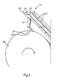
- the optical transfer means 12 is an elongate element of plastic or the like wherein a plurality of self-focussing fibers are provided, the optical axis of the transfer means, or more correctly the optical plane thereof, passing through the axis of the drum.
Landscapes
- Engineering & Computer Science (AREA)
- Multimedia (AREA)
- Signal Processing (AREA)
- Physics & Mathematics (AREA)
- Optics & Photonics (AREA)
- Health & Medical Sciences (AREA)
- General Health & Medical Sciences (AREA)
- Toxicology (AREA)
- General Engineering & Computer Science (AREA)
- General Physics & Mathematics (AREA)
- Theoretical Computer Science (AREA)
- Printers Or Recording Devices Using Electromagnetic And Radiation Means (AREA)
- Dot-Matrix Printers And Others (AREA)
- Exposure Or Original Feeding In Electrophotography (AREA)
- Facsimile Heads (AREA)
- Fax Reproducing Arrangements (AREA)
Applications Claiming Priority (2)
| Application Number | Priority Date | Filing Date | Title |
|---|---|---|---|
| GB8205024 | 1982-02-19 | ||
| GB8205024 | 1982-02-19 |
Publications (3)
| Publication Number | Publication Date |
|---|---|
| EP0086907A2 EP0086907A2 (en) | 1983-08-31 |
| EP0086907A3 EP0086907A3 (en) | 1984-11-28 |
| EP0086907B1 true EP0086907B1 (en) | 1987-05-06 |
Family
ID=10528481
Family Applications (1)
| Application Number | Title | Priority Date | Filing Date |
|---|---|---|---|
| EP82201324A Expired EP0086907B1 (en) | 1982-02-19 | 1982-10-25 | Recording apparatus |
Country Status (5)
| Country | Link |
|---|---|
| US (1) | US4536778A (env) |
| EP (1) | EP0086907B1 (env) |
| JP (1) | JPS58142872A (env) |
| CA (1) | CA1203840A (env) |
| DE (1) | DE3276289D1 (env) |
Families Citing this family (53)
| Publication number | Priority date | Publication date | Assignee | Title |
|---|---|---|---|---|
| JPS58147386A (ja) * | 1982-02-26 | 1983-09-02 | Canon Inc | 印字装置を備えた電子機器 |
| DE3368839D1 (en) * | 1983-01-21 | 1987-02-05 | Agfa Gevaert Nv | Recording apparatus |
| JPS6027565A (ja) * | 1983-07-25 | 1985-02-12 | Mitsubishi Electric Corp | 発光ダイオ−ドアレイヘツドおよびその製造方法 |
| DE3438949C2 (de) * | 1983-10-25 | 1994-03-10 | Canon Kk | Druckvorrichtung |
| DE3376727D1 (en) * | 1983-11-01 | 1988-06-23 | Agfa Gevaert Nv | Recording apparatus |
| WO1986002045A1 (fr) * | 1984-09-27 | 1986-04-10 | Sanyo Electric Co., Ltd. | Tete imprimante optique pour appareil a impression optique |
| JPS61111061A (ja) * | 1984-11-05 | 1986-05-29 | Casio Comput Co Ltd | 記録装置 |
| JPS61160982A (ja) * | 1985-01-08 | 1986-07-21 | Mitsubishi Electric Corp | 発光ダイオ−ドアレイヘツド |
| US4589745A (en) * | 1985-01-25 | 1986-05-20 | Polaroid Corporation | Geometric LED layout for line exposure |
| JPS61211063A (ja) * | 1985-03-15 | 1986-09-19 | Kyocera Corp | 光プリンタヘツド |
| DE3579453D1 (de) * | 1985-04-23 | 1990-10-04 | Agfa Gevaert Nv | Monolithische integration von lichtemittierenden elementen und steuerelektronik. |
| EP0246481B1 (de) * | 1986-05-13 | 1990-12-27 | Heimann GmbH | Kontaktbildsensorzeile |
| US4779108A (en) * | 1986-11-18 | 1988-10-18 | Sanyo Electric Co., Ltd. | Optical printer head |
| JP2816147B2 (ja) * | 1987-03-27 | 1998-10-27 | 株式会社日立製作所 | 発光ダイオードアレイ用駆動回路 |
| US4967192A (en) * | 1987-04-22 | 1990-10-30 | Hitachi, Ltd. | Light-emitting element array driver circuit |
| US4829321A (en) * | 1987-04-23 | 1989-05-09 | Hitachi Cable, Ltd. | Optical printer head with a light emitting diode array |
| US4799071A (en) * | 1987-09-21 | 1989-01-17 | Eastman Kodak Company | Dot printer with age compensation means |
| JPH0712712B2 (ja) * | 1987-10-07 | 1995-02-15 | 双葉電子工業株式会社 | 蛍光プリンタヘッド |
| JPH059616Y2 (env) * | 1987-10-17 | 1993-03-10 | ||
| JP2630960B2 (ja) * | 1987-10-17 | 1997-07-16 | グラフテック株式会社 | サーマルドットアレイを用いた波形記録装置 |
| US4912483A (en) * | 1987-10-22 | 1990-03-27 | Graphtec Kabushiki Kaisha | Balanced head suspension in thermal recorders |
| DE3808636A1 (de) * | 1988-03-15 | 1989-09-28 | Siemens Ag | Zeichengenerator fuer einen nichtmechanischen drucker |
| US4851862A (en) * | 1988-08-05 | 1989-07-25 | Eastman Kodak Company | Led array printhead with tab bonded wiring |
| US4927778A (en) * | 1988-08-05 | 1990-05-22 | Eastman Kodak Company | Method of improving yield of LED arrays |
| US4821051A (en) * | 1988-09-01 | 1989-04-11 | Eastman Kodak Company | Optical printhead having thermal expansion stress relief |
| US4913526A (en) * | 1988-09-01 | 1990-04-03 | Eastman Kodak Company | Optical LED printhead with lens locator bar |
| US4942405A (en) * | 1988-10-11 | 1990-07-17 | Hewlett-Packard Company | Light emitting diode print head assembly |
| US5014074A (en) * | 1988-10-11 | 1991-05-07 | Hewlett-Packard Company | Light emitting diode print head assembly |
| JP2845933B2 (ja) * | 1989-04-24 | 1999-01-13 | キヤノン株式会社 | 記録ヘッドユニット |
| NL8901230A (nl) * | 1989-05-17 | 1990-12-17 | Oce Nederland Bv | Belichtings- en afdrukinrichting. |
| US5317344A (en) * | 1989-12-22 | 1994-05-31 | Eastman Kodak Company | Light emitting diode printhead having improved signal distribution apparatus |
| US5543830A (en) * | 1990-10-12 | 1996-08-06 | Minnesota Mining And Manufacturing Company | Apparatus with light emitting element, microlens and gradient index lens characteristics for imaging continuous tone images |
| EP0507366B1 (en) * | 1991-04-04 | 1996-07-03 | Agfa-Gevaert N.V. | LED exposure head |
| US5818500A (en) * | 1991-05-06 | 1998-10-06 | Eastman Kodak Company | High resolution field emission image source and image recording apparatus |
| US5872587A (en) * | 1991-07-16 | 1999-02-16 | Minolta Co., Ltd. | Light signal generating device with reduced light leakage |
| JP2937577B2 (ja) * | 1991-09-11 | 1999-08-23 | 双葉電子工業 株式会社 | 蛍光プリンタ用光源 |
| NL9101745A (nl) * | 1991-10-18 | 1993-05-17 | Oce Nederland Bv | Belichtings- en afdrukinrichting. |
| CA2077813C (en) * | 1991-12-20 | 1998-07-28 | Thomas L. Paoli | Apparatus and method for spot position control in an output device employing a linear array of light sources |
| US5606358A (en) * | 1991-12-23 | 1997-02-25 | Eastman Kodak Company | Light-emitting diode printhead |
| DE4303225C2 (de) * | 1993-02-04 | 1996-08-14 | Siemens Nixdorf Inf Syst | Optischer Zeichengenerator für einen elektrografischen Drucker |
| DE4308864C2 (de) * | 1992-06-25 | 1996-05-09 | Agfa Gevaert Ag | Vorrichtung zum Kopieren von transparenten Bildvorlagen |
| US5640188A (en) * | 1992-12-18 | 1997-06-17 | Xerox Corporation | Multiple diode laser employing mating substrates |
| JP2845719B2 (ja) * | 1993-04-12 | 1999-01-13 | 沖電気工業株式会社 | ドライバic |
| DE69315566T2 (de) * | 1993-06-18 | 1998-03-26 | Xeikon N.V., Mortsel | Led-Aufzeichnungskopf |
| NL9301330A (nl) * | 1993-07-30 | 1995-02-16 | Oce Nederland Bv | Afdrukinrichting voorzien van een LED-array. |
| US5764273A (en) * | 1993-08-27 | 1998-06-09 | Xerox Corporation | Spot position control using a linear array of light valves |
| US5638108A (en) * | 1994-08-31 | 1997-06-10 | Xerox Corporation | Lower resolution led bars used for 600 SPI printing |
| JP3185204B2 (ja) * | 1995-05-31 | 2001-07-09 | 日本精機株式会社 | 発光素子アセンブリ |
| JP3227385B2 (ja) * | 1996-07-11 | 2001-11-12 | キヤノン株式会社 | 画像形成装置 |
| US7151557B2 (en) * | 2004-03-19 | 2006-12-19 | Lexmark International, Inc. | Collimation assembly for adjusting laser light sources in a multi-beamed laser scanning unit |
| US8096634B2 (en) * | 2007-09-17 | 2012-01-17 | Xerox Corporation | Temperature compensation for full-width arrays write heads |
| GB201209142D0 (en) * | 2012-05-24 | 2012-07-04 | Lumejet Holdings Ltd | Media exposure device |
| JP6156402B2 (ja) * | 2015-02-13 | 2017-07-05 | 日亜化学工業株式会社 | 発光装置 |
Family Cites Families (11)
| Publication number | Priority date | Publication date | Assignee | Title |
|---|---|---|---|---|
| FR2178433A5 (env) * | 1972-03-31 | 1973-11-09 | Radiotechnique Compelec | |
| US3952311A (en) * | 1972-04-24 | 1976-04-20 | The Laitram Corporation | Electro-optical printing system |
| US4455562A (en) * | 1981-08-14 | 1984-06-19 | Pitney Bowes Inc. | Control of a light emitting diode array |
| EP0022704B1 (fr) * | 1979-07-13 | 1983-12-14 | COMPAGNIE INDUSTRIELLE DES TELECOMMUNICATIONS CIT-ALCATEL S.A. dite: | Barrette d'impression d'image, son procédé de fabrication et dispositif d'impression d'image |
| JPS5630154A (en) * | 1979-08-21 | 1981-03-26 | Oki Electric Ind Co Ltd | Photoprint head |
| JPS5710162A (en) * | 1980-06-23 | 1982-01-19 | Nippon Telegr & Teleph Corp <Ntt> | Exposure system of electrophotography |
| CA1175884A (en) * | 1980-06-25 | 1984-10-09 | Hugh St. L. Dannatt | Light emitting diode assembly |
| EP0079904A1 (en) * | 1981-05-26 | 1983-06-01 | PURDY, Haydn Victor | Light emitting diode array devices and image transfer systems |
| US4413269A (en) * | 1981-11-23 | 1983-11-01 | International Business Machines Corporation | Method of and apparatus for controlling gray scale while printing on charge sensitive recording mediums |
| US4427275A (en) * | 1982-07-22 | 1984-01-24 | Pitney Bowes Inc. | Xerographic electronic printer |
| US4455578A (en) * | 1982-08-30 | 1984-06-19 | Eastman Kodak Company | Electronics for arrayed photosources |
-
1982
- 1982-10-25 EP EP82201324A patent/EP0086907B1/en not_active Expired
- 1982-10-25 DE DE8282201324T patent/DE3276289D1/de not_active Expired
- 1982-10-26 US US06/436,671 patent/US4536778A/en not_active Expired - Fee Related
- 1982-11-04 JP JP57194479A patent/JPS58142872A/ja active Granted
- 1982-11-05 CA CA000415021A patent/CA1203840A/en not_active Expired
Also Published As
| Publication number | Publication date |
|---|---|
| EP0086907A2 (en) | 1983-08-31 |
| US4536778A (en) | 1985-08-20 |
| JPS58142872A (ja) | 1983-08-25 |
| EP0086907A3 (en) | 1984-11-28 |
| JPH0342188B2 (env) | 1991-06-26 |
| DE3276289D1 (en) | 1987-06-11 |
| CA1203840A (en) | 1986-04-29 |
Similar Documents
| Publication | Publication Date | Title |
|---|---|---|
| US4536778A (en) | Recording apparatus with modular LED array of higher production yield | |
| EP0115088B1 (en) | Recording apparatus | |
| EP0141880B1 (en) | Recording apparatus | |
| EP0460194B1 (en) | A light emitting diode printhead having improved signal distribution apparatus | |
| EP0098382B1 (en) | Uniformly intense imaging by close-packed lens array | |
| US4706130A (en) | Image recording apparatus utilizing light emitting diodes with pixel shape correction | |
| EP0786353B1 (en) | Led printing head | |
| US4575739A (en) | Recording apparatus | |
| US5134340A (en) | Light-emitting diode printhead | |
| US5274401A (en) | Electrostatic printhead | |
| EP0247699B1 (en) | Image-forming element for an electrostatic printer, and a printer in which an element of this kind is used | |
| GB2099221A (en) | Light emitting diode array devices and image transfer systems | |
| US5257049A (en) | LED exposure head with overlapping electric circuits | |
| US4763041A (en) | Dot array fluorescent tube for writing optical information in optical printer | |
| JP2001130051A (ja) | 露光装置および画像形成装置 | |
| EP0510274A1 (en) | Light emitting diode printhead | |
| EP0453612A1 (en) | Light emitting diode array | |
| WO1982004353A1 (en) | Light emitting diode array devices and image transfer systems | |
| JP2991259B2 (ja) | 画像形成装置 | |
| JP2000174986A (ja) | 露光装置ならびに露光装置を用いた画像形成装置 | |
| JPH08192534A (ja) | Ledプリントヘッド | |
| JPH06334221A (ja) | 画像装置 |
Legal Events
| Date | Code | Title | Description |
|---|---|---|---|
| PUAI | Public reference made under article 153(3) epc to a published international application that has entered the european phase |
Free format text: ORIGINAL CODE: 0009012 |
|
| AK | Designated contracting states |
Designated state(s): BE DE FR GB IT NL |
|
| PUAL | Search report despatched |
Free format text: ORIGINAL CODE: 0009013 |
|
| AK | Designated contracting states |
Designated state(s): BE DE FR GB IT NL |
|
| 17P | Request for examination filed |
Effective date: 19850406 |
|
| 17Q | First examination report despatched |
Effective date: 19860424 |
|
| GRAA | (expected) grant |
Free format text: ORIGINAL CODE: 0009210 |
|
| AK | Designated contracting states |
Kind code of ref document: B1 Designated state(s): BE DE FR GB IT NL |
|
| REF | Corresponds to: |
Ref document number: 3276289 Country of ref document: DE Date of ref document: 19870611 |
|
| ITF | It: translation for a ep patent filed | ||
| ET | Fr: translation filed | ||
| PLBE | No opposition filed within time limit |
Free format text: ORIGINAL CODE: 0009261 |
|
| STAA | Information on the status of an ep patent application or granted ep patent |
Free format text: STATUS: NO OPPOSITION FILED WITHIN TIME LIMIT |
|
| 26N | No opposition filed | ||
| ITTA | It: last paid annual fee | ||
| PGFP | Annual fee paid to national office [announced via postgrant information from national office to epo] |
Ref country code: BE Payment date: 19950821 Year of fee payment: 14 |
|
| PGFP | Annual fee paid to national office [announced via postgrant information from national office to epo] |
Ref country code: NL Payment date: 19951019 Year of fee payment: 14 |
|
| PG25 | Lapsed in a contracting state [announced via postgrant information from national office to epo] |
Ref country code: BE Effective date: 19961031 |
|
| REG | Reference to a national code |
Ref country code: GB Ref legal event code: 746 Effective date: 19961118 |
|
| REG | Reference to a national code |
Ref country code: FR Ref legal event code: D6 |
|
| BERE | Be: lapsed |
Owner name: AGFA-GEVAERT N.V. Effective date: 19961031 |
|
| PG25 | Lapsed in a contracting state [announced via postgrant information from national office to epo] |
Ref country code: NL Effective date: 19970501 |
|
| NLV4 | Nl: lapsed or anulled due to non-payment of the annual fee |
Effective date: 19970501 |
|
| PGFP | Annual fee paid to national office [announced via postgrant information from national office to epo] |
Ref country code: GB Payment date: 19980810 Year of fee payment: 17 |
|
| PGFP | Annual fee paid to national office [announced via postgrant information from national office to epo] |
Ref country code: FR Payment date: 19980922 Year of fee payment: 17 |
|
| PG25 | Lapsed in a contracting state [announced via postgrant information from national office to epo] |
Ref country code: GB Free format text: LAPSE BECAUSE OF NON-PAYMENT OF DUE FEES Effective date: 19991025 |
|
| GBPC | Gb: european patent ceased through non-payment of renewal fee |
Effective date: 19991025 |
|
| PG25 | Lapsed in a contracting state [announced via postgrant information from national office to epo] |
Ref country code: FR Free format text: LAPSE BECAUSE OF NON-PAYMENT OF DUE FEES Effective date: 20000630 |
|
| REG | Reference to a national code |
Ref country code: FR Ref legal event code: ST |
|
| PGFP | Annual fee paid to national office [announced via postgrant information from national office to epo] |
Ref country code: DE Payment date: 20010829 Year of fee payment: 20 |