EP0054079B1 - Convertisseur AN parallèle à MOS - Google Patents
Convertisseur AN parallèle à MOS Download PDFInfo
- Publication number
- EP0054079B1 EP0054079B1 EP80107811A EP80107811A EP0054079B1 EP 0054079 B1 EP0054079 B1 EP 0054079B1 EP 80107811 A EP80107811 A EP 80107811A EP 80107811 A EP80107811 A EP 80107811A EP 0054079 B1 EP0054079 B1 EP 0054079B1
- Authority
- EP
- European Patent Office
- Prior art keywords
- input
- comparator
- comparators
- voltage divider
- transfer transistor
- Prior art date
- Legal status (The legal status is an assumption and is not a legal conclusion. Google has not performed a legal analysis and makes no representation as to the accuracy of the status listed.)
- Expired
Links
Images
Classifications
-
- H—ELECTRICITY
- H04—ELECTRIC COMMUNICATION TECHNIQUE
- H04N—PICTORIAL COMMUNICATION, e.g. TELEVISION
- H04N7/00—Television systems
- H04N7/24—Systems for the transmission of television signals using pulse code modulation
-
- H—ELECTRICITY
- H03—ELECTRONIC CIRCUITRY
- H03M—CODING; DECODING; CODE CONVERSION IN GENERAL
- H03M1/00—Analogue/digital conversion; Digital/analogue conversion
- H03M1/12—Analogue/digital converters
- H03M1/34—Analogue value compared with reference values
- H03M1/36—Analogue value compared with reference values simultaneously only, i.e. parallel type
- H03M1/361—Analogue value compared with reference values simultaneously only, i.e. parallel type having a separate comparator and reference value for each quantisation level, i.e. full flash converter type
Definitions
- the invention relates to parallel-analog-to-digital converters monolithically integrated by means of insulating layer field-effect transistors, that is to say for short MOS-parallel A / D converters.
- the number of binary digits of the digital converter output signal is designated by n.
- All the comparator inputs of one type, for example the non-inverting ones, are connected to the signal input and the comparator inputs of the other type, for example the inverting ones, are each connected to a voltage divider tap.
- the known arrangement provides that during the first half of the clock period the respective voltage divider tap by means of the one CMOS transmission gate lies at the corresponding comparator input via the assigned capacitance, while at the same time the comparator, which is only a CMOS inverter, is normalized to its tipping point via a further CMOS transmission gate.
- the comparator input is connected to the voltage divider via a third, controlled, CMOS transmission gate, while the CMOS inverter is enabled at its breakpoint.
- the invention specified in the claim provides a further solution to the problem of dynamic compensation of MOS parallel A / D converters.
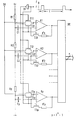
- Each non-inverting input + of the comparators K1 ... Kp lies above the controlled current path of the first transfer transistor T11, T12, T1 p at the signal input SE. Furthermore, the non-inverting input is connected to the associated voltage divider tap via the controlled current path of the second transfer transistor T21, T22, T2p.
- This voltage divider consists of the resistors R1, R2, Rp and is connected to the reference voltage Ur.
- the second transistor T21 is thus at the connection point of the resistors R1, R2, the second transistor T22 at the connection point of the resistor R2 with the next voltage divider resistor, which is no longer shown in the drawing, and the second transistor T2p is at the connection point of the last resistor Rp of the voltage divider the circuit zero.
- fen is also the capacitance C1, C2, Cp, the other end of which is at the inverting input of the associated comparator K1, K2, Kp.
- MOS capacitors are advantageously used, which are then included in the integrated circuit.
- a negative feedback path leads from the output of each comparator K1, K2, Kp to the associated inverting input, which consists of the resistor R'1, R'2, R'p and the controlled current path of the respective third transfer transistor T31, T32, T3p connected in series therewith .
- One end of the controlled current path of the respective third transfer transistor is therefore also at a connection of the corresponding capacitance C1, C2, Cp.
- the gates of the respective second and third transfer transistors T21, T31; T22, T32; T2p, T3p are connected to one another and are connected to a clock signal F that controls them only during the character rewind pulses as short conversion pauses T, the timing of which is indicated schematically in the drawing above right and which also inverts the gates of the first transfer transistors via the inverter IV T11, T12, T1 p controls.
- the Short pauses in conversion T can also be referred to as compensation times, since the dynamic compensation is effective during them.
- the second and third transfer transistors are thus conductive and the first transfer transistors are blocked, it being assumed for the exemplary embodiment of the drawing that the transistors shown therein are p-channel transistors of the enhancement type.
- the voltage at the respective inverting input of the comparators K1, K2, Kp is thus set to the voltage value at the associated voltage divider tap, including the respective offset voltage of the comparators, since via the second transfer transistors the non-inverting input is connected to this potential point, which is otherwise located at the signal input SE.
- the respective capacitance C1, C2, Cp is thus charged to the offset voltage of the associated comparator.
- the second and third transfer transistors are blocked and the first transfer transistors are conductive, so that the input signal is switched through to the non-inverting input and the inverting input is at the potential of the voltage divider tap including the respective offset voltage, so that the capacitances C1 ... Cp form a compensation voltage source for the associated comparators K1 ... Kp during the conversion times t.
Landscapes
- Engineering & Computer Science (AREA)
- Multimedia (AREA)
- Signal Processing (AREA)
- Theoretical Computer Science (AREA)
- Analogue/Digital Conversion (AREA)
Claims (1)
- Convertisseur analogique/numérique parallèle monolithique intégré, du type à transistors à effet de champ à grille isolée (convertisseur A/D MOS parallèle), pour utilisation dans des appareils de télévision, comportant une entrée de signal (SE), des comparateurs (K1, K2, Kp) en nombre p=2n-1, un diviseur de tension constitué de p ou p-1 résistances (R1, R2, Rp) connecté à une tension de référence (Ur), et une partie codeur (DC) reliée aux sorties des comparateurs, ces éléments étant tels que- n désigne le nombre des emplacements binaires du signal de sortie numérique du convertisseur,- tous les comparateurs sont reliés, côté entrée, à l'entrée de signal (SE) par l'intermédiaire du trajet de conduction commandé d'un premier transistor de transfert (T11, T12, T1 p), ainsi que chacun à une prise d'un diviseur de tension, cela par l'intermédiaire du trajet de conduction commandé d'un deuxième transistor de transfert (T21, T22, T2p),- par l'intermédiaire d'une résistance (R'1, R'2, R'p) et du trajet de conduction commandé d'un troisième transistor de transfert (T31, T32, T3p) monté en série avec cette résistance, chaque sortie de comparateur est connectée à une entrée de comparateur, laquelle est reliée à une capacité (C1, C2, Cp), et- les grilles des deuxième et troisième transistors de transfert (T21, T31 ; T22, T32; T2p, T3p) sont mutuellement reliées et reçoivent un signal d'horloge (F) qui en commande la conduction, et les portes des premiers transistors de transfert (T11, T12, T1p) sont aussi reliées entre elles et reçoivent le signal d'horloge inversé, ce convertisseur étant caractérisé par les particularités suivantes:- chaque comparateur possède une entrée non inverseuse reliée à l'entrée de signal (SE), et une entrée inverseuse reliée à la capacité (C1, C2, Cp),- chaque entrée inverseuse (-) du comparateur est connectée par l'intermédiaire de la capacité (C1, C2, Cp), à la prise correspondante du diviseur de tension, et- le signal d'horloge (F) ne commande les deuxièmes et troisièmes transistors de transfert (T21, T31 ; T22, T32; T2p, T3p) que pendant la durée du retour de ligne.
Priority Applications (5)
| Application Number | Priority Date | Filing Date | Title |
|---|---|---|---|
| DE8080107811T DE3069190D1 (de) | 1980-12-11 | 1980-12-11 | Mos-parallel a/d converter |
| EP80107811A EP0054079B1 (fr) | 1980-12-11 | 1980-12-11 | Convertisseur AN parallèle à MOS |
| US06/326,637 US4400693A (en) | 1980-12-11 | 1981-12-02 | MOS Parallel A/D converter |
| JP56197794A JPS57123733A (en) | 1980-12-11 | 1981-12-10 | Mos parallel a/d converter |
| US06/503,229 US4547763A (en) | 1980-12-11 | 1983-06-10 | MOS Parallel A/D converter |
Applications Claiming Priority (1)
| Application Number | Priority Date | Filing Date | Title |
|---|---|---|---|
| EP80107811A EP0054079B1 (fr) | 1980-12-11 | 1980-12-11 | Convertisseur AN parallèle à MOS |
Publications (2)
| Publication Number | Publication Date |
|---|---|
| EP0054079A1 EP0054079A1 (fr) | 1982-06-23 |
| EP0054079B1 true EP0054079B1 (fr) | 1984-09-12 |
Family
ID=8186928
Family Applications (1)
| Application Number | Title | Priority Date | Filing Date |
|---|---|---|---|
| EP80107811A Expired EP0054079B1 (fr) | 1980-12-11 | 1980-12-11 | Convertisseur AN parallèle à MOS |
Country Status (4)
| Country | Link |
|---|---|
| US (2) | US4400693A (fr) |
| EP (1) | EP0054079B1 (fr) |
| JP (1) | JPS57123733A (fr) |
| DE (1) | DE3069190D1 (fr) |
Families Citing this family (25)
| Publication number | Priority date | Publication date | Assignee | Title |
|---|---|---|---|---|
| DE3069190D1 (de) * | 1980-12-11 | 1984-10-18 | Itt Ind Gmbh Deutsche | Mos-parallel a/d converter |
| FR2536923A1 (fr) * | 1982-11-26 | 1984-06-01 | Efcis | Comparateur a prise en memoire de la tension de decalage et application a un convertisseur analogique-numerique a structure parallele |
| US4647968A (en) * | 1984-12-03 | 1987-03-03 | Rca Corporation | Analog-to-digital conversion system as for a narrow bandwidth signal processor |
| US4602241A (en) * | 1985-06-28 | 1986-07-22 | Rca Corporation | Input current saving apparatus for flash A/D converter |
| JPH0754910B2 (ja) * | 1986-03-10 | 1995-06-07 | 株式会社日立製作所 | Ad変換器 |
| US4899153A (en) * | 1986-04-03 | 1990-02-06 | Brooktree Corporation | Fast high-resolution analog-to-digital converter |
| US5173698A (en) * | 1986-12-24 | 1992-12-22 | Zdzislaw Gulczynski | Flash analog-to-digital converter with integrating input stage |
| FR2623668B1 (fr) * | 1987-11-20 | 1990-03-09 | Thomson Composants Militaires | Convertisseur analogique-numerique rapide a structure parallele |
| KR910001911B1 (ko) * | 1988-05-19 | 1991-03-30 | 삼성전자 주식회사 | 전병렬형 Bi-CMOS용 아날로그 디지탈 콘버터 |
| US5214430A (en) * | 1989-01-31 | 1993-05-25 | Zdzislaw Gulczynski | Ladderless true flash analog-to-digital converter with automatic calibration |
| JPH03179920A (ja) * | 1989-12-08 | 1991-08-05 | Mitsubishi Electric Corp | サンプルホールド回路装置 |
| JPH0629850A (ja) * | 1992-05-11 | 1994-02-04 | Takayama:Kk | A/dコンバータ |
| JP3067903B2 (ja) * | 1992-08-20 | 2000-07-24 | 沖電気工業株式会社 | アナログ/ディジタル変換器 |
| US5554986A (en) * | 1994-05-03 | 1996-09-10 | Unitrode Corporation | Digital to analog coverter having multiple resistor ladder stages |
| US5696508A (en) * | 1995-02-24 | 1997-12-09 | Lucent Technologies Inc. | Comparator-offset compensating converter |
| KR100483867B1 (ko) * | 1996-04-01 | 2005-04-20 | 록히드 마틴 코포레이션 | Adc 오프셋 패턴차 제거 방법 및 장치 |
| US5786866A (en) | 1996-10-15 | 1998-07-28 | Fairchild Semiconductor Corporation | Video color subcarrier signal generator |
| US5877718A (en) * | 1997-03-24 | 1999-03-02 | International Business Machines Corporation | Differential analog-to-digital converter with low power consumption |
| US5990814A (en) * | 1997-09-05 | 1999-11-23 | Cirrus Logic, Inc. | Method and circuit for calibration of flash analog to digital converters |
| JP2002533973A (ja) | 1998-12-22 | 2002-10-08 | ビショップ イノヴェーション リミテッド | 容量性フラッシュアナログ−ディジタル変換器用電子回路 |
| US7242330B2 (en) * | 2003-12-17 | 2007-07-10 | Texas Instruments Incorporated | Dynamic compensation of analog-to-digital converter (ADC) offset errors using filtered PWM |
| US7939873B2 (en) * | 2004-07-30 | 2011-05-10 | Semiconductor Energy Laboratory Co., Ltd. | Capacitor element and semiconductor device |
| US10009039B1 (en) * | 2017-08-18 | 2018-06-26 | Cirrus Logic, Inc. | Multi-path analog system with multi-mode high-pass filter |
| US10069483B1 (en) | 2017-08-18 | 2018-09-04 | Cirrus Logic, Inc. | Multi-path analog system with multi-mode high-pass filter |
| US10141946B1 (en) | 2017-08-18 | 2018-11-27 | Cirrus Logic, Inc. | Multi-path analog system with multi-mode high-pass filter |
Family Cites Families (4)
| Publication number | Priority date | Publication date | Assignee | Title |
|---|---|---|---|---|
| US3747089A (en) * | 1971-11-09 | 1973-07-17 | K Sharples | Analog to digital converter |
| US3982241A (en) * | 1974-08-19 | 1976-09-21 | Digital Equipment Corporation | Self-zeroing analog-to-digital conversion system |
| JPS558051B2 (fr) * | 1974-11-06 | 1980-03-01 | ||
| DE3069190D1 (de) * | 1980-12-11 | 1984-10-18 | Itt Ind Gmbh Deutsche | Mos-parallel a/d converter |
-
1980
- 1980-12-11 DE DE8080107811T patent/DE3069190D1/de not_active Expired
- 1980-12-11 EP EP80107811A patent/EP0054079B1/fr not_active Expired
-
1981
- 1981-12-02 US US06/326,637 patent/US4400693A/en not_active Expired - Fee Related
- 1981-12-10 JP JP56197794A patent/JPS57123733A/ja active Pending
-
1983
- 1983-06-10 US US06/503,229 patent/US4547763A/en not_active Expired - Fee Related
Also Published As
| Publication number | Publication date |
|---|---|
| DE3069190D1 (de) | 1984-10-18 |
| US4547763A (en) | 1985-10-15 |
| US4400693A (en) | 1983-08-23 |
| EP0054079A1 (fr) | 1982-06-23 |
| JPS57123733A (en) | 1982-08-02 |
Similar Documents
| Publication | Publication Date | Title |
|---|---|---|
| EP0054079B1 (fr) | Convertisseur AN parallèle à MOS | |
| DE2145295C3 (de) | Schaltungsanordnung für ein Schieberegister | |
| DE2855584A1 (de) | Taktgesteuerter praezisionsvergleicher | |
| DE2310267C2 (de) | Digital/Analog-Umsetzer | |
| DE2711829A1 (de) | Vergleicher fuer einen analog/digital- und digital/analog-umsetzer | |
| DE2556828C3 (de) | Dynamisches Schieberegister aus Isolierschicht-Feldeffekttransistoren | |
| EP0039076A1 (fr) | Circuit intégrateur comportant un étage d'échantillonnage | |
| DE3120669A1 (de) | A/d - und d/a - wandler | |
| DE2801272C2 (de) | Schaltungsanordnung zur Durchführung einer gewichtsfaktorabhängigen Ladungsaufteilung und -übertragung | |
| DE2602382C2 (de) | Reihen-Parallel-Analog-Digital-Umsetzereinrichtung | |
| EP0421395B2 (fr) | Agencement de conversion d'une grandeur électrique d'entrée en un signal électrique continu proportionnel à ladite grandeur | |
| DE2838310B1 (de) | Schaltungsanordnung zur Umsetzung von Digital-Signalen,insbesondere PCM-Signalen,in diesen entsprechende Analog-Signale,mit einem R-2R-Kettennetzwerk | |
| DE3511688C2 (fr) | ||
| DE2836948A1 (de) | Mos-analog/digital-umsetzer | |
| DE2341822C3 (de) | Digitales Schieberegister | |
| DE2612764C2 (de) | Spannungs-Frequenz-Wandler | |
| EP0217120B1 (fr) | Montage d'annulation d'écho | |
| EP0320525A1 (fr) | Etage échantillonneur- bloqueur et son utilisation dans des convertisseurs analogiques/numériques parallèles | |
| EP0012985B1 (fr) | Intégrateur à double rampe | |
| DE3246176A1 (de) | Einrichtung zur offsetkompensation in einer verstaerkerschaltung | |
| DE3027331C2 (de) | Spannungspolaritätsumschaltschaltung | |
| EP0142182B1 (fr) | Montage pour la conversion d'un signal d'entrée numérique en un signal de sortie analogique | |
| DE2241917B2 (de) | Schieberegister | |
| DE3031592A1 (de) | Verfahren zum nullpunktabgleich des durch einen operationsverstaerker realisierten analogwertvergleichers eines unter verwendung eines digital-analog-wandlers nach dem iterativprinzip arbeitenden analog-digital-wandlers, insbesondere bei dessen zugehoerigkeit zu einer einrichtung zur analog-digital-wandlung und umgekehrt zur digital-analog-wandlung (codec) | |
| DE19653192C2 (de) | Monolithisch integrierte Signalverarbeitungsschaltung |
Legal Events
| Date | Code | Title | Description |
|---|---|---|---|
| PUAI | Public reference made under article 153(3) epc to a published international application that has entered the european phase |
Free format text: ORIGINAL CODE: 0009012 |
|
| 17P | Request for examination filed |
Effective date: 19811010 |
|
| AK | Designated contracting states |
Designated state(s): DE FR GB IT NL |
|
| ITF | It: translation for a ep patent filed |
Owner name: AVV. PAOLO SAVI |
|
| GRAA | (expected) grant |
Free format text: ORIGINAL CODE: 0009210 |
|
| AK | Designated contracting states |
Designated state(s): DE FR GB IT NL |
|
| REF | Corresponds to: |
Ref document number: 3069190 Country of ref document: DE Date of ref document: 19841018 |
|
| ET | Fr: translation filed | ||
| PLBE | No opposition filed within time limit |
Free format text: ORIGINAL CODE: 0009261 |
|
| STAA | Information on the status of an ep patent application or granted ep patent |
Free format text: STATUS: NO OPPOSITION FILED WITHIN TIME LIMIT |
|
| 26N | No opposition filed | ||
| GBPC | Gb: european patent ceased through non-payment of renewal fee | ||
| PG25 | Lapsed in a contracting state [announced via postgrant information from national office to epo] |
Ref country code: GB Free format text: LAPSE BECAUSE OF NON-PAYMENT OF DUE FEES Effective date: 19881118 |
|
| REG | Reference to a national code |
Ref country code: FR Ref legal event code: DL |
|
| PGFP | Annual fee paid to national office [announced via postgrant information from national office to epo] |
Ref country code: DE Payment date: 19931210 Year of fee payment: 14 |
|
| PGFP | Annual fee paid to national office [announced via postgrant information from national office to epo] |
Ref country code: FR Payment date: 19931229 Year of fee payment: 14 |
|
| PGFP | Annual fee paid to national office [announced via postgrant information from national office to epo] |
Ref country code: NL Payment date: 19931231 Year of fee payment: 14 |
|
| PG25 | Lapsed in a contracting state [announced via postgrant information from national office to epo] |
Ref country code: NL Effective date: 19950701 |
|
| PG25 | Lapsed in a contracting state [announced via postgrant information from national office to epo] |
Ref country code: FR Effective date: 19950831 |
|
| NLV4 | Nl: lapsed or anulled due to non-payment of the annual fee |
Effective date: 19950701 |
|
| PG25 | Lapsed in a contracting state [announced via postgrant information from national office to epo] |
Ref country code: DE Effective date: 19950901 |
|
| REG | Reference to a national code |
Ref country code: FR Ref legal event code: ST |