EP0048925B1 - Schaltungsanordnung für kleine Fernsprechnebenstellenanlagen mit wechselseitiger Übertragung von binären Digitalsignalen zwischen einer zentralen Einrichtung und mit ihr verbundenen Fernsprechapparaten - Google Patents
Schaltungsanordnung für kleine Fernsprechnebenstellenanlagen mit wechselseitiger Übertragung von binären Digitalsignalen zwischen einer zentralen Einrichtung und mit ihr verbundenen Fernsprechapparaten Download PDFInfo
- Publication number
- EP0048925B1 EP0048925B1 EP81107505A EP81107505A EP0048925B1 EP 0048925 B1 EP0048925 B1 EP 0048925B1 EP 81107505 A EP81107505 A EP 81107505A EP 81107505 A EP81107505 A EP 81107505A EP 0048925 B1 EP0048925 B1 EP 0048925B1
- Authority
- EP
- European Patent Office
- Prior art keywords
- central device
- information
- circuit
- transmission
- voltage
- Prior art date
- Legal status (The legal status is an assumption and is not a legal conclusion. Google has not performed a legal analysis and makes no representation as to the accuracy of the status listed.)
- Expired
Links
- 230000005540 biological transmission Effects 0.000 title claims description 41
- 230000002457 bidirectional effect Effects 0.000 title 1
- 230000011664 signaling Effects 0.000 claims description 16
- 230000008859 change Effects 0.000 claims description 4
- 230000000694 effects Effects 0.000 claims description 3
- 238000010276 construction Methods 0.000 claims description 2
- 230000015572 biosynthetic process Effects 0.000 claims 1
- 230000004048 modification Effects 0.000 claims 1
- 238000012986 modification Methods 0.000 claims 1
- 239000003990 capacitor Substances 0.000 description 10
- 230000010363 phase shift Effects 0.000 description 6
- 230000009467 reduction Effects 0.000 description 6
- 230000006870 function Effects 0.000 description 4
- 230000003287 optical effect Effects 0.000 description 4
- 238000010586 diagram Methods 0.000 description 3
- 230000008878 coupling Effects 0.000 description 2
- 238000010168 coupling process Methods 0.000 description 2
- 238000005859 coupling reaction Methods 0.000 description 2
- 238000011017 operating method Methods 0.000 description 2
- 238000012545 processing Methods 0.000 description 2
- 230000001360 synchronised effect Effects 0.000 description 2
- 230000006978 adaptation Effects 0.000 description 1
- 238000001514 detection method Methods 0.000 description 1
- 238000011161 development Methods 0.000 description 1
- 238000011156 evaluation Methods 0.000 description 1
- 230000000977 initiatory effect Effects 0.000 description 1
- 238000000034 method Methods 0.000 description 1
- 230000008569 process Effects 0.000 description 1
- 230000001105 regulatory effect Effects 0.000 description 1
- 230000035945 sensitivity Effects 0.000 description 1
- 230000001629 suppression Effects 0.000 description 1
Images

Classifications
-
- H—ELECTRICITY
- H04—ELECTRIC COMMUNICATION TECHNIQUE
- H04M—TELEPHONIC COMMUNICATION
- H04M9/00—Arrangements for interconnection not involving centralised switching
- H04M9/002—Arrangements for interconnection not involving centralised switching with subscriber controlled access to a line, i.e. key telephone systems
- H04M9/003—Transmission of control signals from or to the key telephone set; signalling equipment at key telephone set, e.g. keyboard or display equipment
-
- H—ELECTRICITY
- H04—ELECTRIC COMMUNICATION TECHNIQUE
- H04L—TRANSMISSION OF DIGITAL INFORMATION, e.g. TELEGRAPHIC COMMUNICATION
- H04L25/00—Baseband systems
- H04L25/38—Synchronous or start-stop systems, e.g. for Baudot code
- H04L25/40—Transmitting circuits; Receiving circuits
- H04L25/49—Transmitting circuits; Receiving circuits using code conversion at the transmitter; using predistortion; using insertion of idle bits for obtaining a desired frequency spectrum; using three or more amplitude levels ; Baseband coding techniques specific to data transmission systems
- H04L25/4906—Transmitting circuits; Receiving circuits using code conversion at the transmitter; using predistortion; using insertion of idle bits for obtaining a desired frequency spectrum; using three or more amplitude levels ; Baseband coding techniques specific to data transmission systems using binary codes
Definitions
- the invention relates to a circuit arrangement for small private branch exchanges with reciprocal transmission of binary digital signals between a central device and telephone sets which are connected to it in a star-shaped manner via short connecting lines consisting of a two-wire signal line and a two-wire speech line, the information in one direction preferably being bitwise those of the other direction are nested within defined data blocks and the transmission by binary characters is differentiated by their amplitude or their sign and in one direction, preferably pointing from the central device to the telephone sets, relates to the signal line voltages and in the opposite direction to the signal line currents Binary values take place and the transmission from the central device to the telephone sets a much higher density of information than in the opposite direction g is based.
- Small private branch exchanges are assumed, in which a mutually directed signaling takes place between the individual speech devices and a control device common to them. This signaling takes place via a pair of signal wires, which forms the respective connecting line in addition to the pair of speech wires.
- Setting information for optical display elements attached to them which can be implemented, for example, by light-emitting diodes and / or by a display, is primarily transmitted to the speech apparatus.
- the display can be used, for example, to inform the respective subscriber of the dialed-in number or of any fees accrued.
- the busy status of the internal or existing external lines can be indicated by the lighting status of the individual LEDs.
- the information for all display elements present on a speech device can be combined in a data block and transmitted as binary digital signals.
- the O bit can correspond, for example, to the signal voltage idle value, while the 1 bit can represent an active signal in the form of a voltage drop to be carried out.
- the assigned voltage states are controlled by a transmission unit, which in turn is controlled by a control unit contained in the central device, which represents a processor, for example.
- buttons which enable certain operating procedures or by the actuation of which the type of the intended connection can be signaled. A distinction can therefore be made as to whether an internal connection to another intercom of the private branch exchange or an external connection to an intercom of the public network or to an intercom of another dialing private branch exchange is to be established.
- the binary values of the information coming from the telephone sets can be characterized by different signal current values.
- the information for each direction can be combined in a data block.
- the data blocks are transmitted continuously and not only when the information contained in them changes. Bit-wise interleaving of the information to be assigned to the two directions can also be carried out within a data block formed.
- the mutual signaling requires timely coordination in the transmission functions.
- the clock which is the basis for the transmission of the information bits in the telephone set must coincide in time with the clock which determines the transmission of the information bits in the central facility. Since a change in the voltage or the currents on the signal line is carried out during signaling, it must be ensured that the permissible noise voltage is not exceeded by the transmission pulses generated thereby. This must also apply if the four-core connecting cables have a very short cable length.
- the transmitting unit causes the pulses generated by an amplitude change and assigned to a specific binary value to be deformed by means of elements with reactive resistance that a receiving circuit is arranged at the output of the transmitting unit connected to the signal line, which basically corresponds to the receiving circuit which is on other end of the signal line for the registration of these pulses is present that a certain edge of each, registered in the said receiving circuits Im pulses is used to synchronize the relevant unit for clock generation.
- the noise voltage resulting from the signaling in the speech wires is reduced compared to the use of rectangular pulses.
- the permissible noise voltage is not exceeded even with very short subscriber lines.
- a low transmission frequency for example 250 Hz, is used in most applications for the mutual signaling explained at the beginning.
- the harmonics are in a range that is preferably perceived by the ear. Due to the deformation and the associated attenuation of the harmonics, the transmission level can be increased without simultaneously increasing the noise voltage. This results in a reduction in the sensitivity to interference for the transmission carried out.
- a matching receiving circuit is also arranged on the transmitting side. Since the respective pulses registered by them are used as synchronization pulses, a phase shift between the control signal for the respective transmitter unit and the actually transmitted pulse, which occurs during the deformation by means of the elements with reactive resistance, can no longer have an effect. Since, with respect to a given direction, each pulse to be assigned to this direction is synchronized within a data block, the required clock can in each case be derived from an oscillator which, with the simplest construction, can also have a low frequency constancy.
- the deformation mentioned is carried out for those pulses which are generated by the change in amplitude of the signal voltage and are used for the transmission of information from the central device to the respective speech apparatus.
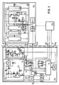
- FIG. 1 shows the basic structure of a small private branch exchange, in which a mutual signaling takes place between the central facility and the individual telephone sets. Only the details necessary for understanding the invention are shown.
- FIG. 2 serve to illustrate the transmission functions.
- the individual speech devices TS1 to TSx are connected in a star shape via a four-wire connection line Ltg to a device ZSt common to them.
- Each subscriber line consists of the pair of speech wires a, b and the pair of signaling wires c, d.
- the voice information and the call stream are transmitted via the a, b wires.
- a mutual signaling between the individual speech devices and the central device is carried out via the c, d wires, and at the same time those units of each speech device which are related to the signaling and which are combined for the speech device TS1 by the module BS, are also used the necessary supply voltage.
- This supply voltage is supplied by the unit SE of the central device.
- This unit can represent a current transformer fed by the mains voltage, which can also emit the supply voltage to be connected to the speech wires for microphone supply in the same way. This is indicated by the multiple symbol on an output of the unit SE.
- the speech circuit SS is connected to the speech wires a, b leading to each speech apparatus, which contains the line termination circuit in addition to the processing of the speech information to be carried out in connection with the handset HA.
- Internal connections can be established between the individual speech devices and there is the possibility of connecting to an external line EL, which can be a line to the public telephone network or to another private branch exchange.
- an external line EL can be a line to the public telephone network or to another private branch exchange.
- four external lines can be available for a total of 16 speech devices, which form the small private branch exchange in connection with the central facility.
- the type of connection desired can be signaled, for example, by pressing the buttons provided for this purpose on each telephone set.
- the possibility is indicated by the keypad TI3 of initiating the transmission of certain information by pressing a key.
- the Tw key is intended to symbolically indicate the keys of a normal dialing keyboard, while the Te key stands for a series of keys through which certain operating procedures can be initiated. If, for example, actuation of a key provided for this purpose, which can be one of the keys Te, signals that the establishment of an external connection is intended, the subsequent actuation of the selection keys leads to the output of the assigned selection information. In systems with normal dialing pulse input by loop interruption, this can take place, controlled by the control unit Pz in the central device by the unit IW. By means of the unit MF there is the possibility of delivering the necessary selection information in a known manner in a multi-frequency code.
- the control unit PZ also provides the setting commands for the coupling arrangement KN, which then enable the connection to be switched through the corresponding actuation of its coupling points. If an internal connection to another speech device of the private branch exchange is desired, the control unit issues corresponding setting commands for the switching network.
- the information transmitted by a speech device can be temporarily stored in a memory (not shown) before processing by the control unit PZ.
- This information can be transmitted by means of binary digital signals, the binary values of which are characterized by a predetermined current idle value or by a current drop in the signal line current.
- This reduction in current can be effected in any telephone set by the transmitting device S, which in turn is controlled by a control unit Pt, which initially receives and processes the stimuli emanating from the keys.
- the lifting of the handset is also registered by this control unit and communicated to the central device as corresponding information.
- the transmitting device S can essentially consist of an electronic switch, by means of which a first of a total of two current regulating units, namely the current regulator unit IR1, which serves to supply the control unit Pt, is deactivated. During this time, the supply of this control unit is maintained by a storage element which is contained in the control unit.
- a second regulator circuit IR2 through which optical display elements, which are symbolically represented by the display element L, are supplied.
- These display elements can represent light-emitting diodes which, for example, indicate the busy status of the individual external lines or the busy status of the internal lines. These light emitting diodes can be connected in series to reduce their current consumption.
- Modulation of the current flowing on the signal line is thus carried out.
- the binary values of the digital information to be transmitted are thus formed by the current reduction, which can correspond to a 1-bit, and for example by the quiescent current value of the signal line, which then corresponds to the 0-bit.
- This information originating from the telephone set can be grouped together in a data block, in which case a data block is alternately transmitted to the central device and from there to the telephone set.
- the information to be provided by a telephone set can also be interleaved bit by bit within a data block to be formed with the information sent out by the central device.
- the digital information provided by the speech apparatus is registered by a receiving circuit E1 to Ex, each coupled to one wire of each signal line, and transferred to the control unit Pz in the central device. So there is a separate receiving circuit for each speech device.
- This receiving circuit can essentially consist of a resistor located in the d-wire and a transistor or operational amplifier evaluating the voltage drop across this resistor.
- the control unit then initiates the subsequent functions to be linked to it.
- the information sent from the central device ZSt to the individual speech apparatuses which mainly relates to setting information for optical display elements, is transmitted as binary digital signals via the respective signal line.
- the binary values of the entire information to be summarized in a data block for a speech apparatus are formed by a voltage rest value and by the voltage drop.
- the same information must be transmitted to the individual speech devices.
- This can be brought about by a common transmission circuit Sz controlled by the control unit Pz, which is connected on the output side in many cases to one wire of the individual signal lines.
- the transmission circuit is coupled to each c-wire.
- the transmission circuit Sz contains a voltage regulator SR, via which a predetermined DC voltage supplied by the unit SE is supplied to the signal line is laid. This serves as the supply voltage for the units coupled to this line in the individual telephone sets.
- the active binary value for example corresponding to a 1-bit, is to be formed by a specific lowering of the signal wire voltage.
- the bit pattern corresponding to the information to be sent out within a data block is emitted by the control unit Pz to the transmission circuit Sz by means of a corresponding transmission clock.
- the transmit clock is applied via the base resistor R5 to the base of the transistor T2 present as a level converter.
- the transistor T2 With each active transmit clock pulse for a bit pattern shown by way of example in line a of FIG. 2, the transistor T2 is turned on.
- potential which drives the resistor R4 and the resistors R2 and R3 is applied to the base of the transistor T1.
- the Zener diode ZD1 is bridged.
- the output voltage of the regulator circuit follows this reduction.
- the voltage on the signal wires thus drops by a certain value, for example by 3 V. Since individual telephone sets can be coupled to the central device directly or via only very short subscriber lines, it must be ensured that no impermissibly high noise voltage is set on the voice line when the pulses are emitted. Since a low transmission frequency of, for example, 250 Hz can be used for the signaling, the harmonics are also at a rectangular pulse in a range in which the ear is very sensitive.
- RC switching elements are provided in the transmission circuit, by means of which the emitted pulses are deformed. This consists essentially in the fact that the corners of the pulses to be emitted are rounded off. This is achieved by the timing elements formed from the resistor R1 and the capacitor C1 as well as from the resistors R2, R3 and the capacitor C2.
- the capacitor C3 connected to the voltage regulator serves to suppress the tendency of the regulator to oscillate.
- This additional transmission circuit then makes it possible to insert an additional information bit at a fixed predetermined location in the data block transmitted by the common transmission circuit Sz for a specific telephone set. This can be done by reducing the voltage on the d-wire, which leads to the telephone set that is to receive the information. As a result, the overall information in question in the respective data block is only evaluated by the receiving circuit contained in this associated telephone set, while it is ignored by the control units of the other telephone sets evaluating the received pulses.
- a selection circuit which is each coupled to a d-wire, can, as shown for the circuit S1, serve a zender diode ZD2 located in this wire, which can be bridged by the transistor T3 to be controlled by the control unit via the resistor R6. If this transistor is switched through by a control pulse supplied by the control unit, the voltage on the signal line is reduced by the value of the Zener voltage. In this way, a 1-bit can be inserted into the data block for a specific telephone set, while a 0-bit is available at this point for all other telephone sets. This then provides the information for these telephone sets that the received data block cannot be evaluated. If information is to be evaluated by all telephone sets, the common transmission circuit Sz in the central device can also transmit the intended selection bit in the data block. It is possible to select a specific telephone set by inserting a selection bit defined by reducing the voltage, since no reference potential is defined in the telephone set for the wires of the signal line.
- the receiving circuit Et located on the signal line evaluates the voltage changes occurring on the wires of the respective signal line. As a result, the information bits defined by a voltage drop can be determined.
- the transistor T6 serves as the receiver for the incoming information bits in the simplest way. Its emitter is connected to the c-wire, while its base is connected via the base resistor R14 to the plus side of the capacitor C5 coupled to the d-wire. This capacitor is charged via the zener diode ZD4 when the transistor T7 is turned on to a voltage which is lower by the zener voltage than the voltage at the c-wire.
- the transmitter circuit in the central device reduces the voltage, the voltage drops, for example, by 3 V, while the voltage across the capacitor C5 keeps the base potential of the transistor T6 approximately constant. If the Zener voltage of the Zender diode ZD4 is chosen so that it together with the base-emitter voltage of the transistor T6 is less than or at most equal to the voltage drop made, the transistor is blocked. The transistor T6 is turned on again at the end of each voltage drop. Every drop in voltage is considered to correspond Appropriate control pulse to the control unit Pt. The voltage drop across the collector resistor R15 is used for this.
- the delay element consisting of resistor R16 and capacitor C6 is also located in the collector circuit. This delay element serves to ensure that brief drops in the signal voltage resulting from interference are not evaluated.
- the active signals emitted by the transmission unit Sz of the central device ZST which are formed by lowering the voltage, are deformed. This is done using components with reactive resistance and serves, in particular with regard to short terminating lines, to reduce the noise voltage on the voice lines.
- the corners of the output pulse are rounded off by RC elements. They are formed from the resistor R1 and the capacitor C1 or from the resistors R2 and R3 and the capacitor C2. As a result of these RC elements, a phase shift arises between the transmit clock pulse, which is supplied by the control unit PZ, and the signal transmitted on the basis of this clock pulse.
- the mutual signaling in which the information is either sent in blocks from the central device to the respective telephone set and then in the opposite direction, or in which the information bits to be mutually assigned in both directions are interleaved within a data block, requires precise timing the respective broadcasting times in the facilities mentioned.
- the clock on which the transmission of the information bits is based in the telephone set must match the clock which determines the transmission of the information bits in the central facility. This requires mutual synchronization of the units from which the clock is derived.
- the clock sequences required for the control unit Pz of the central device ZSt are derived from the oscillator arrangement Oszl.
- the necessary clock sequences for the control unit Pt of the telephone set TS1 are derived from the oscillator arrangement Osz2 with the interposition of divider circuits (not shown). The same applies to the other telephone sets TS.
- the aim is to set up the individual units of small private branch exchanges cost-effectively.
- Simple oscillator circuits are therefore used, the frequency constancy of which makes no high demands.
- this presupposes that they are also synchronized within each transmitted data block, these synchronization pulses being derived from the pulses emitted in a predetermined direction.
- the transmission clock and the pulse received in the individual speech apparatuses on the basis of this transmission clock cannot be used for this synchronization, since the already mentioned phase shift occurs due to the RC elements present for deforming the respective transmission pulses.
- the same simple reception circuit is coupled to the transmission line of the central device as is also used in the individual telephone sets.
- the receiving circuit Ez additionally connected to the transmission line in the central device contains a Zener diode, namely the Zener diode ZD3, for voltage evaluation, in the same way as the receiving circuit Et, which is arranged in each telephone set.
- a certain Zener current is maintained for this Zener diode by the high-resistance resistor R7.
- the voltage drop of the zener diode controls the transistor T4 coupled to it on the emitter side and via the base resistor R8. This transistor has the same function as the transistor T6 in the receiving circuit Et. With R9 the collector resistance of the transistor T4 is designated.
- the voltage drop across this resistor each of which defines an emitted pulse, controls the transistor T5 via the resistor R10.
- the resistor R10 forms a delay element in connection with the capacitor C4, which is present in the receiving circuit Et in the same way. This delay element ensures that interference peaks cannot have an effect.
- the transistor T5 only serves as a level converter.
- the voltage drop occurring at its collector resistor R11 is communicated to the control unit Pz via the resistor R12.
- This control unit can then, for example, detect each falling edge of a transmitted pulse. The same edge is neglected by the control unit at the same time Pt recognized on the basis of the received pulse transmitted to it in the same way.
- Each control unit then derives a synchronization pulse for the oscillator circuit Osz1 or Osz2.
- the receiving unit Ez compared to the receiving unit Et, those components are missing that are there for specific adaptation to the line conditions.
- the influence of the transmission line can be disregarded in the reception circuit Ez, which is arranged at the beginning of the line in relation to the transmission direction.
- the pulse diagram in line a of FIG. 2 shows an example of a bit pattern for a data block to be sent out by the central device.
- Each bit pattern shown corresponds to the transmission clock applied by the control unit Pz to the common transmission circuit Sz.
- the data block which is transmitted continuously and not only when there are changes in information, can begin with a synchronization bit Sy, which can be twice the length of time to distinguish it from the other information bits.
- the information bit Se shown in dashed lines below can be the selection bit described, which is inserted into the data block for selection of a specific telephone set by one of the selection circuits S1 to Sx. In the example, the bit sequence »0, 1, 0, 1 is added. The location of these bits in the data block determines the control address for individual optical display elements.
- the lighting status of these display elements is determined by this bit sequence. With a transmitted 1-bit, for example, the information is to be coupled that the assigned display element is activated. If this represents a light-emitting diode, it is in its light-up state. This is ensured by appropriate control signals from the control unit of the relevant telephone set.
- an acknowledgment bit Q and a parity bit P can follow.
- a pause of the same length is inserted between the information bits.
- an information bit sent by the telephone can be inserted as a 0 or 1 bit in the bitwise nesting.
- Line b shows the voltage curve on the signal line which results from the transmission clock specified by the control unit according to line a.
- each clock pulse leads to a lowering of the signal voltage.
- This 1-bit is thus defined by this reduction from the signal voltage idle value Ur to the value Us.
- This phase shift results from RC elements which are switched on in the transmitter circuit in order to deform the emitted pulses on the transmitter side.
- the necessary reduction in noise voltage is achieved even in cases where a speech device is connected to the central device via a very short connecting line.
- the transmitted pulse is received during its pulse time tz and fed to the respective control unit Pz or Pt.
- Each falling edge can be used to synchronize the existing oscillator circuits. This is indicated by the index SI in line b.
- an information bit can now be sent from the respective telephone set to the central facility.
Landscapes
- Engineering & Computer Science (AREA)
- Signal Processing (AREA)
- Physics & Mathematics (AREA)
- Spectroscopy & Molecular Physics (AREA)
- Computer Networks & Wireless Communication (AREA)
- Sub-Exchange Stations And Push- Button Telephones (AREA)
- Telephonic Communication Services (AREA)
- Meter Arrangements (AREA)
- Interconnected Communication Systems, Intercoms, And Interphones (AREA)
Priority Applications (1)
| Application Number | Priority Date | Filing Date | Title |
|---|---|---|---|
| AT81107505T ATE6719T1 (de) | 1980-09-25 | 1981-09-21 | Schaltungsanordnung fuer kleine fernsprechnebenstellenanlagen mit wechselseitiger uebertragung von binaeren digitalsignalen zwischen einer zentralen einrichtung und mit ihr verbundenen fernsprechapparaten. |
Applications Claiming Priority (2)
| Application Number | Priority Date | Filing Date | Title |
|---|---|---|---|
| DE3036182 | 1980-09-25 | ||
| DE3036182A DE3036182C2 (de) | 1980-09-25 | 1980-09-25 | Verfahren zur wechselseitigen Übertragung von binären Digitalsignalen zwischen einer zentralen Einrichtung und mit ihr verbundenen Fernsprechteilnehmerstellen |
Publications (2)
| Publication Number | Publication Date |
|---|---|
| EP0048925A1 EP0048925A1 (de) | 1982-04-07 |
| EP0048925B1 true EP0048925B1 (de) | 1984-03-14 |
Family
ID=6112832
Family Applications (1)
| Application Number | Title | Priority Date | Filing Date |
|---|---|---|---|
| EP81107505A Expired EP0048925B1 (de) | 1980-09-25 | 1981-09-21 | Schaltungsanordnung für kleine Fernsprechnebenstellenanlagen mit wechselseitiger Übertragung von binären Digitalsignalen zwischen einer zentralen Einrichtung und mit ihr verbundenen Fernsprechapparaten |
Country Status (12)
| Country | Link |
|---|---|
| EP (1) | EP0048925B1 (enExample) |
| AR (1) | AR230911A1 (enExample) |
| AT (1) | ATE6719T1 (enExample) |
| AU (1) | AU543544B2 (enExample) |
| BR (1) | BR8106120A (enExample) |
| CA (1) | CA1185024A (enExample) |
| DE (1) | DE3036182C2 (enExample) |
| FI (1) | FI74567C (enExample) |
| GB (1) | GB2085695B (enExample) |
| IN (1) | IN155068B (enExample) |
| NO (1) | NO153589C (enExample) |
| TR (1) | TR21185A (enExample) |
Families Citing this family (2)
| Publication number | Priority date | Publication date | Assignee | Title |
|---|---|---|---|---|
| DE3248276A1 (de) * | 1982-12-28 | 1984-06-28 | Standard Elektrik Lorenz Ag, 7000 Stuttgart | Schnittstellenschaltung fuer ein fernmeldesystem |
| DE4107593C1 (enExample) * | 1991-03-09 | 1992-05-21 | Fraunhofer-Gesellschaft Zur Foerderung Der Angewandten Forschung Ev, 8000 Muenchen, De |
Family Cites Families (3)
| Publication number | Priority date | Publication date | Assignee | Title |
|---|---|---|---|---|
| US3215779A (en) * | 1961-02-24 | 1965-11-02 | Hallicrafters Co | Digital data conversion and transmission system |
| CA1018270A (en) * | 1972-05-23 | 1977-09-27 | Itt Canada | Key telephone system using time division and space division control |
| US4046972A (en) * | 1976-10-27 | 1977-09-06 | Bell Telephone Laboratories, Incorporated | Key telephone station set circuit |
-
1980
- 1980-09-25 DE DE3036182A patent/DE3036182C2/de not_active Expired
-
1981
- 1981-09-10 IN IN1017/CAL/81A patent/IN155068B/en unknown
- 1981-09-18 AR AR286801A patent/AR230911A1/es active
- 1981-09-21 EP EP81107505A patent/EP0048925B1/de not_active Expired
- 1981-09-21 NO NO813203A patent/NO153589C/no unknown
- 1981-09-21 AT AT81107505T patent/ATE6719T1/de not_active IP Right Cessation
- 1981-09-24 AU AU75644/81A patent/AU543544B2/en not_active Ceased
- 1981-09-24 GB GB8128946A patent/GB2085695B/en not_active Expired
- 1981-09-24 CA CA000386626A patent/CA1185024A/en not_active Expired
- 1981-09-24 BR BR8106120A patent/BR8106120A/pt unknown
- 1981-09-24 FI FI812977A patent/FI74567C/fi not_active IP Right Cessation
- 1981-09-24 TR TR21185A patent/TR21185A/xx unknown
Also Published As
| Publication number | Publication date |
|---|---|
| DE3036182C2 (de) | 1983-12-01 |
| FI74567B (fi) | 1987-10-30 |
| AU7564481A (en) | 1982-04-01 |
| AU543544B2 (en) | 1985-04-26 |
| CA1185024A (en) | 1985-04-02 |
| EP0048925A1 (de) | 1982-04-07 |
| GB2085695B (en) | 1984-09-12 |
| NO813203L (no) | 1982-03-26 |
| NO153589C (no) | 1986-04-16 |
| IN155068B (enExample) | 1984-12-29 |
| BR8106120A (pt) | 1982-06-15 |
| GB2085695A (en) | 1982-04-28 |
| TR21185A (tr) | 1983-12-06 |
| AR230911A1 (es) | 1984-07-31 |
| FI74567C (fi) | 1988-02-08 |
| NO153589B (no) | 1986-01-06 |
| ATE6719T1 (de) | 1984-03-15 |
| DE3036182A1 (de) | 1982-04-01 |
| FI812977L (fi) | 1982-03-26 |
Similar Documents
| Publication | Publication Date | Title |
|---|---|---|
| EP0028416B1 (de) | Breitband-Vermittlungssystem | |
| DE2351104C3 (de) | Nach dem Zeitmultiplexverfahren arbeitende Fernsprechvermittlungsanlage | |
| DE3204228A1 (de) | Synchronisiereinrichtung fuer eine digitale fernmeldeanlage, insbesondere fuer eine ueber eine fernsprechleitung angeschaltete fernmeldeendstelle | |
| DE3204227A1 (de) | Digitale fernmeldeendstelle zur uebertragung von informationen zu einer digitalen fernmeldeanlage, insbesondere zu einer fernsprechanlage bzw. fernsprechnebenstellenanlage | |
| DE3204226A1 (de) | Gleichstrom-/gleichstrom-umsetzer zur verwendung in einer peripheren einrichtung einer fernmeldeanlage, insbesondere in einer digitalen fernmeldeendstelle | |
| EP0048925B1 (de) | Schaltungsanordnung für kleine Fernsprechnebenstellenanlagen mit wechselseitiger Übertragung von binären Digitalsignalen zwischen einer zentralen Einrichtung und mit ihr verbundenen Fernsprechapparaten | |
| DE2546422C2 (de) | Zweidraht-Vollduplex-Datenübertragungsverfahren und Vorrichtung zur Ausführung des Verfahrens | |
| DE2718317A1 (de) | Digital koppelnde fernmeldevermittlungseinrichtung | |
| DE3036240C2 (de) | Verfahren zur Übertragung von Binärzeichen zwischen einer zentralen Einrichtung und einer Anzahl von Teilnehmerstellen bei Fernsprechvermittlungsanlagen | |
| DE3427139A1 (de) | Einrichtung zur uebertragung von daten ueber eine fernsprechleitung | |
| EP0061524B1 (de) | Verfahren zur wechselseitigen Übertragung von binären Daten-signalen über eine beidseitig mit einem Übertrager abgeschlossene Signalleitung | |
| DE3783909T2 (de) | Anordnung zur berichtsmeldung in einem fernsprechsystem. | |
| DE3036183C2 (de) | Schaltungsanordnung zur Aussendung von digitalen Datensignalen von einer zentralen Einrichtung zu Teilnehmerstellen kleiner Nebenstellenanlagen | |
| DE2614334C3 (enExample) | ||
| DE3036204C2 (de) | Empfangsschaltung in kleinen Fernsprech-Nebenstellenanlagen für über das Signalisierungsadernpaar einer vieradrigen Teilnehmeranschlußleitung übertragene binäre Digitalsignale, deren Binärwerte unterschiedlichen Spannungswerten entsprechen | |
| DE3434853C2 (enExample) | ||
| DE3014420C2 (de) | Schaltungsanordnung zur Erzeugung eines akustischen Signals an Teilnehmerstellen in Fernsprech-, insbesondere Fernsprechnebenstellenanlagen | |
| DE2821513C3 (de) | Schaltungsanordnung zur Einspeisung von Hörtönen in Fernsprechvermittlungsanlagen | |
| DE3112894C2 (de) | Sende- und Empfangseinheit für in Fernsprechvermittlungsanlagen, insbesondere in kleinen Nebenstellenanlagen zu übertragende binäre Steuerdatensignale | |
| DE3114738A1 (de) | Schaltungsanordnung fuer einen fernsprechreihenapparat | |
| DE1762969C (de) | Schaltungsanordnung zum Anzeigen der Berechtigungsklasse in Fernmeldevermittlungsanlagen. Ausscheidung aus: 1412985 | |
| DE2019800C3 (de) | Übertragungssystem für den internen und externen Datenverkehr einer Fernmelde-, insbesondere Fernsprechanlage | |
| AT392378B (de) | Einrichtung zur uebertragung von daten ueber eine fernsprechleitung | |
| EP0246480B1 (de) | Schaltungsanordnung in Fernsprechvermittlungsanlagen zur Auswertung von Binärzeichen, deren Binärwerte jeweils durch festgelegte sich voneinander unterscheidende Stromwerte gebildet werden | |
| DE3036205A1 (de) | Verfahren zur wechselseitigen uebertragung von binaeren digitalsignalen zwischen einer zentralen einrichtung und mit ihr verbundenen endeinrichtung |
Legal Events
| Date | Code | Title | Description |
|---|---|---|---|
| PUAI | Public reference made under article 153(3) epc to a published international application that has entered the european phase |
Free format text: ORIGINAL CODE: 0009012 |
|
| 17P | Request for examination filed |
Effective date: 19811028 |
|
| AK | Designated contracting states |
Designated state(s): AT BE IT NL |
|
| ITF | It: translation for a ep patent filed | ||
| GRAA | (expected) grant |
Free format text: ORIGINAL CODE: 0009210 |
|
| AK | Designated contracting states |
Designated state(s): AT BE IT NL |
|
| REF | Corresponds to: |
Ref document number: 6719 Country of ref document: AT Date of ref document: 19840315 Kind code of ref document: T |
|
| PLBE | No opposition filed within time limit |
Free format text: ORIGINAL CODE: 0009261 |
|
| STAA | Information on the status of an ep patent application or granted ep patent |
Free format text: STATUS: NO OPPOSITION FILED WITHIN TIME LIMIT |
|
| 26N | No opposition filed | ||
| ITTA | It: last paid annual fee | ||
| PGFP | Annual fee paid to national office [announced via postgrant information from national office to epo] |
Ref country code: AT Payment date: 19900830 Year of fee payment: 10 |
|
| PGFP | Annual fee paid to national office [announced via postgrant information from national office to epo] |
Ref country code: BE Payment date: 19900913 Year of fee payment: 10 |
|
| PGFP | Annual fee paid to national office [announced via postgrant information from national office to epo] |
Ref country code: NL Payment date: 19900930 Year of fee payment: 10 |
|
| PG25 | Lapsed in a contracting state [announced via postgrant information from national office to epo] |
Ref country code: AT Effective date: 19910921 |
|
| PG25 | Lapsed in a contracting state [announced via postgrant information from national office to epo] |
Ref country code: BE Effective date: 19910930 |
|
| BERE | Be: lapsed |
Owner name: SIEMENS A.G. BERLIN UND MUNCHEN Effective date: 19910930 |
|
| PG25 | Lapsed in a contracting state [announced via postgrant information from national office to epo] |
Ref country code: NL Effective date: 19920401 |
|
| NLV4 | Nl: lapsed or anulled due to non-payment of the annual fee |