EP0019142B1 - Dispositif de mémoire à régénération interne - Google Patents
Dispositif de mémoire à régénération interne Download PDFInfo
- Publication number
- EP0019142B1 EP0019142B1 EP80102315A EP80102315A EP0019142B1 EP 0019142 B1 EP0019142 B1 EP 0019142B1 EP 80102315 A EP80102315 A EP 80102315A EP 80102315 A EP80102315 A EP 80102315A EP 0019142 B1 EP0019142 B1 EP 0019142B1
- Authority
- EP
- European Patent Office
- Prior art keywords
- signal
- refresh
- address
- row
- strobe signal
- Prior art date
- Legal status (The legal status is an assumption and is not a legal conclusion. Google has not performed a legal analysis and makes no representation as to the accuracy of the status listed.)
- Expired
Links
Images


Classifications
-
- G—PHYSICS
- G11—INFORMATION STORAGE
- G11C—STATIC STORES
- G11C11/00—Digital stores characterised by the use of particular electric or magnetic storage elements; Storage elements therefor
- G11C11/21—Digital stores characterised by the use of particular electric or magnetic storage elements; Storage elements therefor using electric elements
- G11C11/34—Digital stores characterised by the use of particular electric or magnetic storage elements; Storage elements therefor using electric elements using semiconductor devices
- G11C11/40—Digital stores characterised by the use of particular electric or magnetic storage elements; Storage elements therefor using electric elements using semiconductor devices using transistors
- G11C11/401—Digital stores characterised by the use of particular electric or magnetic storage elements; Storage elements therefor using electric elements using semiconductor devices using transistors forming cells needing refreshing or charge regeneration, i.e. dynamic cells
- G11C11/406—Management or control of the refreshing or charge-regeneration cycles
Definitions
- the present invention relates to a memory device composed of semiconductor elements and, more particularly, to a refreshing system for a dynamic type memory device using insulated-gate field-effect transistors.
- RAMs Dynamic type random access memories
- MOSTEK Co. of U.S.A. which allows an internal refresh in which a refresh operation for memory cells is internally performed without receiving any refresh address information from the outside thereof by using a refresh control signal in addition to the conventional external refresh which requires refresh address information from the outside.
- This RAM achieves high-flexibility in control and its application.
- a dynamic random access memory the input signals of which comprise a row strobe signal, a column strobe signal, a multi-address input signal, and a refresh control signal, having a function that, first by enabling the row strobe signal to incorporate the address input as a row address information, a circuit involved automatically refreshes data stored in all the memory cells on a row line designated by the address input at this time in an external refresh, and then by enabling the column strobe signal, the circuit automatically transfers data between a selected memory cell on the column line designated by the address input at this time and a data input/output circuit, and having a refresh address means designating a row in which when said refresh control signal is enabled, an internal refresh is automatically performed, and at the end of the internal refresh operation, a first confirmation signal is produced from an internal circuit; and at the end of a reset precharge operation, a second confirmation signal is produced from the internal circuit.
- the refresh control signal When the refresh control signal is enabled during the active period of the row strobe signal, it is latched by the internal circuit.
- the internal circuit receives the latched refresh control signal to automatically effect the internal refresh.
- the circuit automatically enters the reset precharge period and subsequently the reset precharge state is continued.
- the chip enable signal CE as a basic clock shifts from high level to low level and the RAM enters an active period
- an address input information at that time point is held (latched) and the contents of memory cells on a selected word (row) line are refreshed at the same time.
- data of a memory cell of the selected column and on the selected word line is transferred to a data bus and then is amplified by an output amplifier.
- the output enable signal OE controls as to if the read out data is made to appear at the input/output common terminal or not.
- the signal OE is set to low level, the output data is obtained at the input/output common terminal (read cycle).
- the data is written into a selected memory cell by shifting the signal WEto a low level to be enabled during the active period.
- the signal OE must be at its inactive level, i.e. at high level (write cycle). The reason for this is that if the signal OEis enabled i.e. low level, the read signal appears at the input/output common terminal, and it competes with the write input data. Therefore, in a read modify write cycle, after the signal OE is enabled i.e. low level in the RAM to read out the data, the signal OE is disenabled i.e. high level to be reset and then the signal WE is turned to its enabled level i.e. low level to write the data.
- the refresh operation of the memory "MK 4816" is as described above.
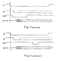
- this refresh operation is applied to the multi-address input system which has two clock signals that is a row strobe signal RAS and a column strobe signal CAS and address signals are inputted in a multiple manner into a RAM as previously described, the following problems arise.
- the two-clock, multi-address system is substantially a standard system in the MOS dynamic RAM with a large capacity, for example 4K, 16K and 64K.
- the Signal RAS is at its active level (low level)
- the address information at that time point is latched as a row address information and the contents of all the memory cells on the word line specified by the row address information are refreshed.
- the signal CAS When the signal CAS is at its active level (low level), the address information at that time is latched as a column address information, and a selected memory cell of the column designated is coupled with a data input/output circuit. Under this condition, the read or the write operation is performed. Therefore, the signal RAS and CAS are not related to the signals CE and OE respectively by one to one correspondence.
- the external refresh of MODE (1) in this system is exactly the same as the conventional one.
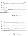
- MODE (3) corresponds to a case that the signal RFSH is at the active level during the reset period of the inactive level of the signal RAS. This operation is relatively easily performed since it is realized by providing the refresh cycle in the reset precharge state.
- the refresh mode due to MODE (4) is a refresh mode where the signal RFSH is kept at a low level for a long period and all the input signals other than the signal RFSH are inhibited from inputting into the RAM whereby the refresh of the RAM is automatically performed under control of the internal circuit alone. Accordingly, this refresh mode is also possible in the two-clock, multi-address input system in question.
- the problem resides in the application of the refresh mode "MODE (2)" to the two-clock, multi-address input system.
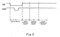
- the circuit upon the-active level of the signal OE or WE, after the data is read out or after the completion of the write operation is confirmed, the circuit is automatically shifted to the reset precharge phase, and following the completion thereof the internal refresh operation is introduced.
- MODE (2) refresh operation corresponds to a case that the signa) RFSH is turned to its active level during the active level period of the signal HAS in the read or write cycle.
- the refresh operation after the completion of the enabled access operation, the reset precharge is automatically performed and then the refresh cycle must be peformed.
- the output data appears as a result of the active level of the signal OEin the read cycle.
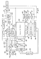
- the signal RFSH may be enabled at any time position in the active period of the signal RAS and is latched in an internal circuit of a RAM.
- the signalRFSH remains latched during an active period T1 of the signal RAS and until the signal RAS is turned to the inactive level to be reset.
- whole RAM circuit enters a reset precharge period T2 and a confirmation signal representing a confirmation of the end of the reset precharge operation is produced.
- the circuit When the internal refresh operation completes, the circuit automatically enters reset precharge period T4 where the content of the refresh address counter is incremented and the circuit prepares for the next internal refresh operation. Accordingly, the circuit waites the next activation (active level) of the RFSH or RAS while it is in the reset precharge state.
- the internal refresh by enabling the signal RFSH during the reset precharge (inactive level) period of the signal RAS, immediately following the activation of the signal RFSH, the internal refresh is performed immediately following confirmation of the end of the reset precharge operation, and the circuit automatically enters the reset precharge period after the internal refresh is completed.
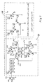
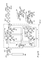
- FIG. 6 A circuit structure of the RAM due to the two-clock, multi-address system (multi-address type RAM), which employs the internal refresh system according to the invention, is illustrated in Fig. 6.
- the way of inputting the signal RFSH classifies the operation of the multi-address type RAM into the following four modes:
- the operation mode of (1) is a normal circuit operation.
- a RAS series clock generating circuit 115 operates to produce a series of internal control signals.
- the address input 119 at that time point is latched by a row address inverter buffer 118 as a row address, and the output of the row address inverter buffer 118 is determined.
- a row decoder 116 performs the selecting operation of a word (a row) line in a memory cell matrix 101. Finally, memory cells in the memory matrix 101 on the word line specified by the row address input are refreshed (external refresh).
- a CAS series clock generating circuit 108 produces a series of control signals.
- the address input 119 at that time point is latched as a column address by a column address inverter buffer 104 in response to one of the CAS series control signals, and the output of a column address inverter buffer 104 is determined.
- a column decoder 103 performs the selecting operation of a memory cell belonging to the selected word line in the memory matrix 101, and a selected memory cell on the column selected is coupled with a data input/output bus DB through a sense amplifier, and a data input/output (I/O) gate portion 102.
- read data from the selected memory cell appears at an output terminal DATA OUT, through a data output buffer 105.
- a write clock generating circuit 107 starts to operate in response to the activation of the write enable signal WE.
- the output of a data input buffer 106 is enabled in accordance with a level of a signal at a data input terminal DATA IN at this time, so that data is written into a selected memory cell.
- the operation mode of (2) is an internal refresh mode enabling the present invention to be effective.
- the signal RFSH if the signal RFSH is enabled, the signal RFSH is immediately latched in an internal refresh control clock generating circuit 109.
- the active operation of the cycle is continued while the internal refresh operation is not performed. That is, the latch operation of the signal RFSH is independently performed in the refresh control clock generating circuit 109.
- RAS series clock generating circuit 115 is reset and the CAS series clock generating circuit 108 and the write clock generating circuit 107 are in turn reset.
- precharge confirmation signal PEND representing the confirmation of the completion is produced by a precharge detection circuit 122.
- the internal refresh control clock generating circuit 109 enables a cycle signal for the internal refresh and applies it to a RAS input buffer control logic unit 114.
- a RAS series clock generating circuit 115 operates while at the same time the CAS series clock generating circuit 108 and the write clock generating circuit 107 are inhibited from operating by a signal path R4 from the internal refresh control clock generating circuit 109.
- the output signal RCOUT from the refresh address counter 113 are transferred to the row decoder 116 through a multiplexer 117 thereby to refresh memory cells on the word line designated.
- a refresh confirmation signal AEND is produced by a refresh detection circuit 121, so that the cycle signal of the internal refresh is reset and the content of the refresh address counter 113 is incremented for the next interval refresh.
- the precharge detection circuit 122 and the refresh detection circuit 121 operate based on the timing signals produced by the circuit 115.
- the RAS series clock generator 115 enters the reset precharge period. Subsequently, this state is kept up.
- the internal refresh control clock generating circuit 109 When the signal RFSH is enabled during the reset period of the RAS in the operation mode (3), the internal refresh control clock generating circuit 109 immediately operates and, in response to the precharge confirmation signal of the end of the reset precharge operation, the cycle signal of the internal refresh is enabled.
- the RAS series clock generating circuit 115 operates through the RAS input buffer control logic unit 114 to refresh memory cells on the word line designated by the refresh address counter 113. After the operation of the refresh is completed, the cycle signal (R1-R4) of the internal refresh is reset and the refresh address counter 113 is incremented, so that the whole system enters the reset precharge period.
- the operation mode (4) corresponds to a case that the signal RFSH is enabled for a predetermined time period or more and, in this mode, "AUTO REFRESH" is performed.
- an output with a fixed period of an oscillator circuit 111 is necessary which is commonly used for a substrate bias voltage generating circuit 110, normally.
- the cycle signals (R1-R4) for the AUTO REFRESH are enabled to operate the RAS series clock generating circuit 115, through the HAS input buffer control logic unit 114. As a result, memory cells on the word line specified by the refresh address counter 113 are refreshed.
- the RAS input buffer control logic unit 144 rejects the inputting thereto but' accepts only the cycle signal (R1) of the AUTO REFRESH which occurs periodically. Accordingly, the cycle signal (R1) of AUTO REFRESH superposes the operation of the whole circuit, so that the increment of the refresh address counter 113 and the reset precharge operation are kept up after its completion so long as the signal RFSH is kept low level.
- Figs. 7 to 15 illustrating detailed circuit diagrams of the RAM and Fig. 16 illustrating a timing diagram useful in explaining the operation of the embodiment.
- the explanation will proceed with relation to the operation modes (1) to (4), for ease of explanation.
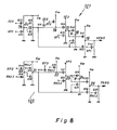
- the timing signals to control the internal refresh such as RF1, RFAA1, RFPP1, RFAA2, RFPP2, and ARO which are produced from the circuit 109 in Fig. 6 are all in low level in Fig. 7.
- a node 1 of the RAS input buffer control logic unit 114 becomes low in level (V DD -threshold voltage), so that the level of RAS appears at node 2 as it is.
- the RAS series clock generating circuit 115 operates with an interrelation as shown in Fig. 7.
- the enable timing signals such as RAS, RASO, RAS1,... SE3 successively rise thereby to refresh the memory cell on the selected word line.
- the signal CAS is enabled, so that the selected memory cell is coupled to the data input/output circuit (106 or 105). As a result, the contents of the memory cell is read out or input data is written into the memory cell in accordance with the signal WE.
- the refresh detection circuit 121 produces the active operation (read and early write) end confirmation signal AEND in response to the final enable timing SE3 produced by the circuit 115.
- the precharge detection circuit 122 produces the reset precharge operation end confirmation signal PEND in response to the final precharge timing XP3. Detailed structures of the refresh detection circuit 121 and the precharge detection circuit 122 are shown in Fig. 8.
- Fig. 9 when the signal RFSH is enabled, the signal RF firstly rises to the V DD (power voltage) level and then the signal RFP shifts to a low level and further the signal RF1 rises to the level V DD .
- V DD power voltage
- Those three timing signals exhibit level change in synchronism with the signal RFSH.
- the waveforms illustrating the operation of the mode (2) performed when the internal refresh system according to the present invention is used are illustrated in Fig. 16.
- @ designates an active period, a reset precharge period, ® an internal refresh period, and INC a time point that the refresh address counter is incremented.
- signals RASR and XPR are synchronized with the signal RAS and are an active timing signal and a reset precharge timing signal, which are isolated from the part of the internal refresh control clock generating circuit (109) in Fig. 9.
- a signal at the node 37 rises only during the active period of the RAS.
- a buffer circuit comprised of MOSTs Q 80 to Q 89 responds to the rise of the signal at the node 37, so that a signal at a node 42 rise to reach V DD level.
- a signal at node 40 shifts to ground potential and the MOST Q 86 become nonconductive. And the node 42 is isolated from the signal RF1 and it is kept at the V DD level during the remaining active period of RAS.
- a MOST Qg o charges a node 43 to a (V DD -threshold voltage) level.
- a node 46 also has the same level by a signal RASR. With a MOST Q 94 having a much larger current ability than a MOST Q 93 , the signal RFAA1 is kept at low level.
- the signal RASR shifts to low level and the signal XPR rises to the V OD level.
- the node 42 shifts to ground potential by the XPR while the node 43 is still kept at the (V DD -threshold voltage) dynamically.
- the confirmation signal PEND is issued and the node 46 shifts to low level, as that the MOST Q 94 becomes nonconductive and the signal RFAA1 rises to reach the V DD level.
- the MOST 0 3 conducts to shift the node 1 to low level so that the MOST Q 7 is nonconductive to isolate the signal RAS from the node 2.
- the MOST Qg also conducts and the node 2 shifts to ground potential, and further the signal RAS rises so that the RAS series clock generating circuit 115 enters the active period.
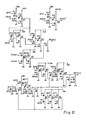
- Th row decoder 116 is constructed as shown in Fig. 15 and provided with the multiplexer 117 so that either the output of the address inverter buffer 118 or the output of the refresh address counter 113 serves as decoder input.
- a node B2 becomes ground potential
- the MOST QQ 5 becomes nonconductive so that the address inverter output and the decoder input are isolated from one another, while at the same time the output from the refresh address counter 113 is transferred through the MOST QQ 6 to the decoder input.
- the memory cells on the selected word line are refreshed.
- the rise of the signal RFAA1 restricts an output CAS of the first stage of the CAS series clock generator circuit 108 to be low level, so that the CAS series clock generating circuit 108 can not operate and only the refresh operation of the row side is performed.
- the signal at the node 48 in Fig. 10 follows the rise of the signal AEND, so that MOSTs Q 91 and Q 95 conduct to shift the signal RFAA1 to ground potential.
- the refresh address counter 113, a first and a second stages CNT1 and CNT2 which are shown in Fig.
- the signal RAS rises and the RAS series clock generating circuit 115 enters the active period.
- the signal RFAA1 cells on the word line designated by the refresh address counter 113 are refreshed, and the operation is completed to rise the signal AEND.
- the signal RFAA2 shifts to ground potential, as is apparent from Fig. 12.
- the signal RFPP2 rises.
- the content of the refresh address counter 113 is incremented while the signal level at the node 1 in Fig. 7 rises to the (V DD -threshold voltage) level.
- the signal RAS of high level appears at the node 2 through the MOST Q 7 . Accordingly, the RAS series clock generating circuit 115 enters the reset precharge period and the operation ends. At this time, the circuit operation in the case of the mode (3) terminates.
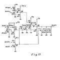
- the AUTO REFRESH which is introduced when the signal RFSH of the mode (4) is enabled for a given period of time or longer, is controlled by the circuit shown in Fig. 13.
- the auto refresh timing generator circuit 112 is made of a counter including a plurality stages of master-slave flip-flop circuits 112-0-112-n. During the period of time that the signal RFSH is in high level, the counter is set to the initial condition and it shifts to low level to be enabled. At this time, the output signal from the oscillator circuit 111 is transferred to MOST QHO.
- the output ARCYC from the final stage 112-n of the counter determines the timing of the AUTO REFRESH and at the intial stage the RFSH shifts to low level and after a given time the ARCYC shifts to low level.
- the signal ARO rise and the signal level at the node 2 in Fig. 7 shifts to ground potential.
- the RAS series clock generating circuit enters the active period.
- the refresh operation in this case is quite similar to that of the case of the signal RFAA1 or RFAA2. After the refresh operation completes and the signal AEND rises, the ARO in Fig. 13 shifts to low level, and the signal level at the node 2 rises.
- the RAS series clock generating circuit 115 enters the reset precharge period. Subsequently, it is left in the reset precharge state until the signal ARCYC changes from high level to low level. So long as the signal RFSH is kept at low level, the RF1 is in high level and the signal level at node 1 in Fig. 7 is in low level. The signal RAS is isolated from the node 2.
- the operation of the RAS series clock generating circuit 115 is controlled by the signal ARC and the signal ARO. Since the signal ARCYC is a counter response for the output signal from the oscillator circuit 111, it takes a waveshape with a given cycle during the period the signal RFSH is in low level. The internal refresh automatically continues.
- the memory circuit when receiving a refresh control signal RFSH enabled during the active period of the row strobe signal RAS, the memory circuit latches it by an internal circuit. Then row strobe signal RAS is reset, and the circuit enters the reset precharge period. The latched state of RFSH is kept until a signal for confirming the end of the reset precharge operation is produced. When the confirmation signal rises, the circuit receives the latch signal to automatically enter the internal refresh period. As a result, memory cells on the word line corresponding to the row address designated by the refresh address counter are refreshed. When the internal refresh operation ends, a confirmation signal is produced and the circuit automatically enters the reset precharge period. Subsequently, the circuit keeps the reset precharge state.
- the internal refresh is applicable for the refresh control signal which is enabled during the active period of the row strobe signal RAS in the dynamic RAM of the two-clock, multi-address system. A flexible use of the RAM is attained in the practical use.
Landscapes
- Engineering & Computer Science (AREA)
- Microelectronics & Electronic Packaging (AREA)
- Computer Hardware Design (AREA)
- Dram (AREA)
Claims (5)
Applications Claiming Priority (2)
| Application Number | Priority Date | Filing Date | Title |
|---|---|---|---|
| JP56160/79 | 1979-05-08 | ||
| JP5616079A JPS55150192A (en) | 1979-05-08 | 1979-05-08 | Memory unit |
Publications (3)
| Publication Number | Publication Date |
|---|---|
| EP0019142A2 EP0019142A2 (fr) | 1980-11-26 |
| EP0019142A3 EP0019142A3 (en) | 1982-11-10 |
| EP0019142B1 true EP0019142B1 (fr) | 1985-07-03 |
Family
ID=13019334
Family Applications (1)
| Application Number | Title | Priority Date | Filing Date |
|---|---|---|---|
| EP80102315A Expired EP0019142B1 (fr) | 1979-05-08 | 1980-04-29 | Dispositif de mémoire à régénération interne |
Country Status (4)
| Country | Link |
|---|---|
| US (1) | US4334295A (fr) |
| EP (1) | EP0019142B1 (fr) |
| JP (1) | JPS55150192A (fr) |
| DE (1) | DE3070827D1 (fr) |
Families Citing this family (40)
| Publication number | Priority date | Publication date | Assignee | Title |
|---|---|---|---|---|
| JPS5873096A (ja) * | 1981-10-27 | 1983-05-02 | Nec Corp | 半導体メモリ |
| JPS58155596A (ja) * | 1982-03-10 | 1983-09-16 | Hitachi Ltd | ダイナミツク型mosram |
| JPS5952495A (ja) * | 1982-09-17 | 1984-03-27 | Hitachi Ltd | Mos−ram装置 |
| JPS59129987A (ja) * | 1983-01-14 | 1984-07-26 | Nec Corp | 半導体メモリ |
| US4587559A (en) * | 1983-03-11 | 1986-05-06 | Welch Allyn, Inc. | Refreshing of dynamic memory |
| JPS59167898A (ja) * | 1983-03-14 | 1984-09-21 | Nec Corp | メモリ回路 |
| US4672583A (en) * | 1983-06-15 | 1987-06-09 | Nec Corporation | Dynamic random access memory device provided with test circuit for internal refresh circuit |
| JPS6061992A (ja) * | 1983-09-14 | 1985-04-09 | Nec Corp | 擬似スタティックメモリ |
| JPS60211692A (ja) * | 1984-04-06 | 1985-10-24 | Hitachi Ltd | 半導体記憶装置 |
| US4622668A (en) * | 1984-05-09 | 1986-11-11 | International Business Machines Corporation | Process and apparatus for testing a microprocessor and dynamic ram |
| JP2631973B2 (ja) * | 1984-07-26 | 1997-07-16 | 三菱電機株式会社 | ダイナミツクメモリ装置 |
| JPS6166295A (ja) * | 1984-09-10 | 1986-04-05 | Nec Corp | 半導体メモリ |
| JPS6212991A (ja) * | 1985-07-10 | 1987-01-21 | Fujitsu Ltd | 半導体記憶装置 |
| US4691303A (en) * | 1985-10-31 | 1987-09-01 | Sperry Corporation | Refresh system for multi-bank semiconductor memory |
| JPS6355797A (ja) * | 1986-08-27 | 1988-03-10 | Fujitsu Ltd | メモリ |
| JPS63166093A (ja) * | 1986-12-26 | 1988-07-09 | Toshiba Corp | 半導体メモリの制御回路 |
| US5313428A (en) * | 1987-11-12 | 1994-05-17 | Sharp Kabushiki Kaisha | Field memory self-refreshing device utilizing a refresh clock signal selected from two separate clock signals |
| US5724540A (en) * | 1988-03-28 | 1998-03-03 | Hitachi, Ltd. | Memory system having a column address counter and a page address counter |
| US5335336A (en) * | 1988-03-28 | 1994-08-02 | Hitachi, Ltd. | Memory device having refresh mode returning previous page address for resumed page mode |
| US5430681A (en) * | 1989-05-08 | 1995-07-04 | Hitachi Maxell, Ltd. | Memory cartridge and its memory control method |
| EP0425693B1 (fr) * | 1989-05-08 | 1996-09-04 | Hitachi Maxell, Ltd. | Cartouche memoire et procede de commande de memoire |
| JP3155545B2 (ja) * | 1990-09-07 | 2001-04-09 | シャープ株式会社 | メモリのリフレッシュ制御回路 |
| KR970004746B1 (ko) * | 1990-11-16 | 1997-04-03 | 세끼자와 다다시 | 고속 어드레스 디코더를 포함하는 반도체 메모리 |
| US5365487A (en) * | 1992-03-24 | 1994-11-15 | Texas Instruments Incorporated | DRAM power management with self-refresh |
| KR960009960B1 (ko) * | 1994-03-12 | 1996-07-25 | 금성일렉트론 주식회사 | 디램의 리프레쉬 콘트롤회로 |
| JPH0955098A (ja) * | 1995-08-15 | 1997-02-25 | Mitsubishi Electric Corp | 半導体記憶装置 |
| US6209071B1 (en) | 1996-05-07 | 2001-03-27 | Rambus Inc. | Asynchronous request/synchronous data dynamic random access memory |
| US6263448B1 (en) | 1997-10-10 | 2001-07-17 | Rambus Inc. | Power control system for synchronous memory device |
| US6092212A (en) * | 1997-12-22 | 2000-07-18 | Intel Corporation | Method and apparatus for driving a strobe signal |
| US6334167B1 (en) | 1998-08-31 | 2001-12-25 | International Business Machines Corporation | System and method for memory self-timed refresh for reduced power consumption |
| US7099221B2 (en) * | 2004-05-06 | 2006-08-29 | Micron Technology, Inc. | Memory controller method and system compensating for memory cell data losses |
| US20060010339A1 (en) * | 2004-06-24 | 2006-01-12 | Klein Dean A | Memory system and method having selective ECC during low power refresh |
| US7340668B2 (en) * | 2004-06-25 | 2008-03-04 | Micron Technology, Inc. | Low power cost-effective ECC memory system and method |
| US7116602B2 (en) | 2004-07-15 | 2006-10-03 | Micron Technology, Inc. | Method and system for controlling refresh to avoid memory cell data losses |
| JP4848564B2 (ja) * | 2005-09-29 | 2011-12-28 | 株式会社ハイニックスセミコンダクター | 半導体メモリ装置のリセット制御回路 |
| KR100832020B1 (ko) * | 2005-09-29 | 2008-05-26 | 주식회사 하이닉스반도체 | 반도체 메모리 장치의 리셋제어회로 |
| US20080080284A1 (en) * | 2006-09-15 | 2008-04-03 | Peter Mayer | Method and apparatus for refreshing memory cells of a memory |
| US7894289B2 (en) | 2006-10-11 | 2011-02-22 | Micron Technology, Inc. | Memory system and method using partial ECC to achieve low power refresh and fast access to data |
| US7900120B2 (en) * | 2006-10-18 | 2011-03-01 | Micron Technology, Inc. | Memory system and method using ECC with flag bit to identify modified data |
| CN109499085A (zh) | 2014-06-11 | 2019-03-22 | 英尼奥斯欧洲股份公司 | 丙烯腈回收的乙腈移除步骤中的污染减轻 |
Family Cites Families (2)
| Publication number | Priority date | Publication date | Assignee | Title |
|---|---|---|---|---|
| US3737879A (en) * | 1972-01-05 | 1973-06-05 | Mos Technology Inc | Self-refreshing memory |
| US3969706A (en) * | 1974-10-08 | 1976-07-13 | Mostek Corporation | Dynamic random access memory misfet integrated circuit |
-
1979
- 1979-05-08 JP JP5616079A patent/JPS55150192A/ja active Granted
-
1980
- 1980-04-29 EP EP80102315A patent/EP0019142B1/fr not_active Expired
- 1980-04-29 DE DE8080102315T patent/DE3070827D1/de not_active Expired
- 1980-05-01 US US06/145,537 patent/US4334295A/en not_active Expired - Lifetime
Non-Patent Citations (2)
| Title |
|---|
| ELECTRONICS, vol. 52, no. 4, 15th February 1979, pages 141-147, New York (USA); D.C. Ford et al: "64-K dynamic RAM has pin that refreshes". * |
| IEEE INTERNATIONAL SOLID-STATE CIRCUITS CONFERENCE, 15th February 1979, pages 144,145,289, New York (USA); S.S.EATON: "A 5V-Only 2Kx8 Dynamic RAM" * |
Also Published As
| Publication number | Publication date |
|---|---|
| JPS6336080B2 (fr) | 1988-07-19 |
| EP0019142A2 (fr) | 1980-11-26 |
| JPS55150192A (en) | 1980-11-21 |
| US4334295A (en) | 1982-06-08 |
| DE3070827D1 (en) | 1985-08-08 |
| EP0019142A3 (en) | 1982-11-10 |
Similar Documents
| Publication | Publication Date | Title |
|---|---|---|
| EP0019142B1 (fr) | Dispositif de mémoire à régénération interne | |
| US4768171A (en) | Memory circuit having a plurality of cell arrays | |
| US5193072A (en) | Hidden refresh of a dynamic random access memory | |
| US5754486A (en) | Self-test circuit for memory integrated circuits | |
| US4672583A (en) | Dynamic random access memory device provided with test circuit for internal refresh circuit | |
| KR920001758B1 (ko) | 내부 셀프-리프레쉬 회로를 가지는 의사(pseudo)-정적 메모리장치 | |
| US4627032A (en) | Glitch lockout circuit for memory array | |
| US4207618A (en) | On-chip refresh for dynamic memory | |
| US5299168A (en) | Circuit for detecting refresh address signals of a semiconductor memory device | |
| JP2856598B2 (ja) | ダイナミックランダムアクセスメモリ装置 | |
| US4322825A (en) | Flexible hidden refresh memory circuit | |
| US4570242A (en) | Dynamic random-access memory | |
| JPS6213758B2 (fr) | ||
| US4494222A (en) | Processor system using on-chip refresh address generator for dynamic memory | |
| US4439843A (en) | Memory device | |
| JPS63127492A (ja) | 半導体記憶装置 | |
| US5007028A (en) | Multiport memory with improved timing of word line selection | |
| US4293932A (en) | Refresh operations for semiconductor memory | |
| JPS5856287A (ja) | 半導体回路 | |
| US4476548A (en) | Dynamic type MOS memory device | |
| US4823322A (en) | Dynamic random access memory device having an improved timing arrangement | |
| EP0458213B1 (fr) | Circuit de commande pour commander un mode d'opération dans une RAM pseudo-statique | |
| KR100221748B1 (ko) | 리프레쉬 기능이 없는 dram 구성의 캐쉬 메모리 장치 | |
| US4695980A (en) | Integrated circuit having a common input terminal | |
| US5327387A (en) | Dynamic random access memory having an improved operational stability |
Legal Events
| Date | Code | Title | Description |
|---|---|---|---|
| PUAI | Public reference made under article 153(3) epc to a published international application that has entered the european phase |
Free format text: ORIGINAL CODE: 0009012 |
|
| AK | Designated contracting states |
Designated state(s): DE FR GB NL |
|
| 17P | Request for examination filed |
Effective date: 19811027 |
|
| PUAL | Search report despatched |
Free format text: ORIGINAL CODE: 0009013 |
|
| AK | Designated contracting states |
Designated state(s): DE FR GB NL |
|
| RAP1 | Party data changed (applicant data changed or rights of an application transferred) |
Owner name: NEC CORPORATION |
|
| GRAA | (expected) grant |
Free format text: ORIGINAL CODE: 0009210 |
|
| AK | Designated contracting states |
Designated state(s): DE FR GB NL |
|
| REF | Corresponds to: |
Ref document number: 3070827 Country of ref document: DE Date of ref document: 19850808 |
|
| ET | Fr: translation filed | ||
| PLBE | No opposition filed within time limit |
Free format text: ORIGINAL CODE: 0009261 |
|
| STAA | Information on the status of an ep patent application or granted ep patent |
Free format text: STATUS: NO OPPOSITION FILED WITHIN TIME LIMIT |
|
| 26N | No opposition filed | ||
| ITCP | It: supplementary protection certificate |
Spc suppl protection certif: CCP 178 |
|
| PGFP | Annual fee paid to national office [announced via postgrant information from national office to epo] |
Ref country code: FR Payment date: 19990409 Year of fee payment: 20 |
|
| PGFP | Annual fee paid to national office [announced via postgrant information from national office to epo] |
Ref country code: NL Payment date: 19990426 Year of fee payment: 20 |
|
| PGFP | Annual fee paid to national office [announced via postgrant information from national office to epo] |
Ref country code: GB Payment date: 19990428 Year of fee payment: 20 |
|
| PGFP | Annual fee paid to national office [announced via postgrant information from national office to epo] |
Ref country code: DE Payment date: 19990430 Year of fee payment: 20 |
|
| PG25 | Lapsed in a contracting state [announced via postgrant information from national office to epo] |
Ref country code: GB Free format text: LAPSE BECAUSE OF EXPIRATION OF PROTECTION Effective date: 20000428 |
|
| PG25 | Lapsed in a contracting state [announced via postgrant information from national office to epo] |
Ref country code: NL Free format text: LAPSE BECAUSE OF EXPIRATION OF PROTECTION Effective date: 20000429 |
|
| REG | Reference to a national code |
Ref country code: GB Ref legal event code: PE20 Effective date: 20000428 |
|
| NLV7 | Nl: ceased due to reaching the maximum lifetime of a patent |
Effective date: 20000429 |