EP0018501B1 - Verfahren zur Herstellung von hochverdichteten vertikalen FETs und eine daraus gebildete Matrixanordnung - Google Patents
Verfahren zur Herstellung von hochverdichteten vertikalen FETs und eine daraus gebildete Matrixanordnung Download PDFInfo
- Publication number
- EP0018501B1 EP0018501B1 EP80101629A EP80101629A EP0018501B1 EP 0018501 B1 EP0018501 B1 EP 0018501B1 EP 80101629 A EP80101629 A EP 80101629A EP 80101629 A EP80101629 A EP 80101629A EP 0018501 B1 EP0018501 B1 EP 0018501B1
- Authority
- EP
- European Patent Office
- Prior art keywords
- layer
- doped
- silicon
- shaped openings
- openings
- Prior art date
- Legal status (The legal status is an assumption and is not a legal conclusion. Google has not performed a legal analysis and makes no representation as to the accuracy of the status listed.)
- Expired
Links
Images




Classifications
-
- G—PHYSICS
- G11—INFORMATION STORAGE
- G11C—STATIC STORES
- G11C11/00—Digital stores characterised by the use of particular electric or magnetic storage elements; Storage elements therefor
- G11C11/21—Digital stores characterised by the use of particular electric or magnetic storage elements; Storage elements therefor using electric elements
- G11C11/34—Digital stores characterised by the use of particular electric or magnetic storage elements; Storage elements therefor using electric elements using semiconductor devices
- G11C11/35—Digital stores characterised by the use of particular electric or magnetic storage elements; Storage elements therefor using electric elements using semiconductor devices with charge storage in a depletion layer, e.g. charge coupled devices
-
- G—PHYSICS
- G11—INFORMATION STORAGE
- G11C—STATIC STORES
- G11C11/00—Digital stores characterised by the use of particular electric or magnetic storage elements; Storage elements therefor
- G11C11/21—Digital stores characterised by the use of particular electric or magnetic storage elements; Storage elements therefor using electric elements
- G11C11/34—Digital stores characterised by the use of particular electric or magnetic storage elements; Storage elements therefor using electric elements using semiconductor devices
- G11C11/40—Digital stores characterised by the use of particular electric or magnetic storage elements; Storage elements therefor using electric elements using semiconductor devices using transistors
- G11C11/401—Digital stores characterised by the use of particular electric or magnetic storage elements; Storage elements therefor using electric elements using semiconductor devices using transistors forming cells needing refreshing or charge regeneration, i.e. dynamic cells
- G11C11/403—Digital stores characterised by the use of particular electric or magnetic storage elements; Storage elements therefor using electric elements using semiconductor devices using transistors forming cells needing refreshing or charge regeneration, i.e. dynamic cells with charge regeneration common to a multiplicity of memory cells, i.e. external refresh
- G11C11/404—Digital stores characterised by the use of particular electric or magnetic storage elements; Storage elements therefor using electric elements using semiconductor devices using transistors forming cells needing refreshing or charge regeneration, i.e. dynamic cells with charge regeneration common to a multiplicity of memory cells, i.e. external refresh with one charge-transfer gate, e.g. MOS transistor, per cell
-
- H—ELECTRICITY
- H10—SEMICONDUCTOR DEVICES; ELECTRIC SOLID-STATE DEVICES NOT OTHERWISE PROVIDED FOR
- H10B—ELECTRONIC MEMORY DEVICES
- H10B12/00—Dynamic random access memory [DRAM] devices
- H10B12/01—Manufacture or treatment
- H10B12/02—Manufacture or treatment for one transistor one-capacitor [1T-1C] memory cells
- H10B12/03—Making the capacitor or connections thereto
- H10B12/038—Making the capacitor or connections thereto the capacitor being in a trench in the substrate
- H10B12/0383—Making the capacitor or connections thereto the capacitor being in a trench in the substrate wherein the transistor is vertical
-
- H—ELECTRICITY
- H10—SEMICONDUCTOR DEVICES; ELECTRIC SOLID-STATE DEVICES NOT OTHERWISE PROVIDED FOR
- H10B—ELECTRONIC MEMORY DEVICES
- H10B12/00—Dynamic random access memory [DRAM] devices
- H10B12/30—DRAM devices comprising one-transistor - one-capacitor [1T-1C] memory cells
- H10B12/39—DRAM devices comprising one-transistor - one-capacitor [1T-1C] memory cells the capacitor and the transistor being in a same trench
- H10B12/395—DRAM devices comprising one-transistor - one-capacitor [1T-1C] memory cells the capacitor and the transistor being in a same trench the transistor being vertical
-
- H—ELECTRICITY
- H10—SEMICONDUCTOR DEVICES; ELECTRIC SOLID-STATE DEVICES NOT OTHERWISE PROVIDED FOR
- H10D—INORGANIC ELECTRIC SEMICONDUCTOR DEVICES
- H10D30/00—Field-effect transistors [FET]
- H10D30/60—Insulated-gate field-effect transistors [IGFET]
- H10D30/63—Vertical IGFETs
-
- H—ELECTRICITY
- H10—SEMICONDUCTOR DEVICES; ELECTRIC SOLID-STATE DEVICES NOT OTHERWISE PROVIDED FOR
- H10W—GENERIC PACKAGES, INTERCONNECTIONS, CONNECTORS OR OTHER CONSTRUCTIONAL DETAILS OF DEVICES COVERED BY CLASS H10
- H10W10/00—Isolation regions in semiconductor bodies between components of integrated devices
- H10W10/01—Manufacture or treatment
- H10W10/011—Manufacture or treatment of isolation regions comprising dielectric materials
- H10W10/014—Manufacture or treatment of isolation regions comprising dielectric materials using trench refilling with dielectric materials, e.g. shallow trench isolations
- H10W10/0143—Manufacture or treatment of isolation regions comprising dielectric materials using trench refilling with dielectric materials, e.g. shallow trench isolations comprising concurrently refilling multiple trenches having different shapes or dimensions
-
- H—ELECTRICITY
- H10—SEMICONDUCTOR DEVICES; ELECTRIC SOLID-STATE DEVICES NOT OTHERWISE PROVIDED FOR
- H10W—GENERIC PACKAGES, INTERCONNECTIONS, CONNECTORS OR OTHER CONSTRUCTIONAL DETAILS OF DEVICES COVERED BY CLASS H10
- H10W10/00—Isolation regions in semiconductor bodies between components of integrated devices
- H10W10/10—Isolation regions comprising dielectric materials
- H10W10/17—Isolation regions comprising dielectric materials formed using trench refilling with dielectric materials, e.g. shallow trench isolations
-
- Y—GENERAL TAGGING OF NEW TECHNOLOGICAL DEVELOPMENTS; GENERAL TAGGING OF CROSS-SECTIONAL TECHNOLOGIES SPANNING OVER SEVERAL SECTIONS OF THE IPC; TECHNICAL SUBJECTS COVERED BY FORMER USPC CROSS-REFERENCE ART COLLECTIONS [XRACs] AND DIGESTS
- Y10—TECHNICAL SUBJECTS COVERED BY FORMER USPC
- Y10S—TECHNICAL SUBJECTS COVERED BY FORMER USPC CROSS-REFERENCE ART COLLECTIONS [XRACs] AND DIGESTS
- Y10S148/00—Metal treatment
- Y10S148/05—Etch and refill
-
- Y—GENERAL TAGGING OF NEW TECHNOLOGICAL DEVELOPMENTS; GENERAL TAGGING OF CROSS-SECTIONAL TECHNOLOGIES SPANNING OVER SEVERAL SECTIONS OF THE IPC; TECHNICAL SUBJECTS COVERED BY FORMER USPC CROSS-REFERENCE ART COLLECTIONS [XRACs] AND DIGESTS
- Y10—TECHNICAL SUBJECTS COVERED BY FORMER USPC
- Y10S—TECHNICAL SUBJECTS COVERED BY FORMER USPC CROSS-REFERENCE ART COLLECTIONS [XRACs] AND DIGESTS
- Y10S148/00—Metal treatment
- Y10S148/051—Etching
-
- Y—GENERAL TAGGING OF NEW TECHNOLOGICAL DEVELOPMENTS; GENERAL TAGGING OF CROSS-SECTIONAL TECHNOLOGIES SPANNING OVER SEVERAL SECTIONS OF THE IPC; TECHNICAL SUBJECTS COVERED BY FORMER USPC CROSS-REFERENCE ART COLLECTIONS [XRACs] AND DIGESTS
- Y10—TECHNICAL SUBJECTS COVERED BY FORMER USPC
- Y10S—TECHNICAL SUBJECTS COVERED BY FORMER USPC CROSS-REFERENCE ART COLLECTIONS [XRACs] AND DIGESTS
- Y10S148/00—Metal treatment
- Y10S148/085—Isolated-integrated
-
- Y—GENERAL TAGGING OF NEW TECHNOLOGICAL DEVELOPMENTS; GENERAL TAGGING OF CROSS-SECTIONAL TECHNOLOGIES SPANNING OVER SEVERAL SECTIONS OF THE IPC; TECHNICAL SUBJECTS COVERED BY FORMER USPC CROSS-REFERENCE ART COLLECTIONS [XRACs] AND DIGESTS
- Y10—TECHNICAL SUBJECTS COVERED BY FORMER USPC
- Y10S—TECHNICAL SUBJECTS COVERED BY FORMER USPC CROSS-REFERENCE ART COLLECTIONS [XRACs] AND DIGESTS
- Y10S148/00—Metal treatment
- Y10S148/117—Oxidation, selective
-
- Y—GENERAL TAGGING OF NEW TECHNOLOGICAL DEVELOPMENTS; GENERAL TAGGING OF CROSS-SECTIONAL TECHNOLOGIES SPANNING OVER SEVERAL SECTIONS OF THE IPC; TECHNICAL SUBJECTS COVERED BY FORMER USPC CROSS-REFERENCE ART COLLECTIONS [XRACs] AND DIGESTS
- Y10—TECHNICAL SUBJECTS COVERED BY FORMER USPC
- Y10S—TECHNICAL SUBJECTS COVERED BY FORMER USPC CROSS-REFERENCE ART COLLECTIONS [XRACs] AND DIGESTS
- Y10S148/00—Metal treatment
- Y10S148/131—Reactive ion etching rie
Definitions
- the invention relates to a method and its modifications for producing high-density vertical FETs which are dielectrically insulated from one another, and to a matrix arrangement formed from such FETs according to the preambles of claims 1, 6 and 11.
- MOSFET circuits for producing matrix memories are known per se.
- US-A-4 017 883 describes a matrix memory for random access with charge-coupled memory cells which have been formed in a semiconductor body which is divided into three contiguous regions along the planar surface of the semiconductor body. Contamination was diffused into the first area, so that it alternatively serves as a source and drain for charge carriers.
- the second or gate region has a threshold voltage that is determined by an impurity that has been introduced into this region either by means of diffusion or ion implantation.
- the third or memory area has a lower threshold voltage than the gate area.
- a single, uniform metal electrode extends over the second and third regions.
- US Pat. No. 3,975,221 also describes a MOS field-effect transistor (MOSFET) with V-shaped trenches, which is provided with a surface-diffused drain and a common substrate source. A heavily doped base layer and a weakly doped space charge region are arranged between the drain and source regions.
- the gate is formed on the inclined surface of the V-shaped trench, which penetrates into the transistor to the substrate and exposes the base layer to the gate structure.
- the gate is formed in the V-shaped trench by an insulating silicon dioxide layer and a conductive gate layer. Suitable lines contact the gate conductor and the drain connection.
- the V-shaped trench is made by anisotropic silicon etching.
- the directional etching process in the ⁇ 100> planes of the silicon proceeds at a much higher speed than in the ⁇ 111> planes, which leads to a sharp, chisel-shaped V-trench geometry.
- a VMOS memory cell of random access memory was specified, in which the storage node is designed as a buried N + -doped zone.
- a V-shaped trench is etched in the top of a buried N + -doped storage node in each cell. All four sides of this V-trench are conductive during a read or write operation.
- US-A-4104 086 describes methods for forming U-shaped trenches in monocrystalline silicon using reactive ion etching.
- the shape of the trenches can be designed so that they have a slight slope preferably between 2 ° and 20 ° with respect to the vertical.
- Filling the trench with dielectric insulation material, such as silicon dioxide, is also described so as to provide a pattern of dielectric insulation for a number of monocrystalline silicon regions.
- a memory matrix which has channels of an FET realized on the wall of a V-shaped opening, in which polycrystalline silicon doped as gate connection is applied to the gate in the V-shaped opening and in which parts of a further doped polycrystalline silicon layer connected to the gate connections and applied on an insulating surface layer form the word lines and in which N + -doped single-crystalline silicon regions adjoining the V-shaped opening form the bit lines.
- the invention has now set itself the task of specifying a method by means of which memory cells of very small dimensions, in particular for read / write memories for random access, can be produced.
- a particularly dense matrix structure from such memory cells is to be specified.
- the invention achieves the advantage that very dense matrices can be produced from FETs, which are dielectrically separated from one another and which have a plurality of vertical or slightly U-shaped trenches that are inclined relative to the vertical.
- the inversion charge storage area is primarily determined by the depth of the trench.
- the density of such a U-shaped MOS single-electrode memory structure for random access is thus considerably greater than in the case of a single-electrode VMOS memory structure.
- the proposed vertical MOSFET memory structure for random access only one of four side walls of the trench is conductive.
- This random access memory is thus about half the size of a VMOS memory, which was described in the article at the aforementioned IEEE International Solid-State Circuit Conference, with half as much memory and with half as much bit line diffusion areas.
- the density of the structure improved by the invention is about twice as high as the comparison type, the capacity ratio between memory and bit line remaining approximately the same.
- the thin silicon dioxide gate isolation region has undergone a fourfold reduction, so that the reliability of such a memory is also better.
- the methods for producing a matrix of highly compressed MOSFETs that are dielectrically insulated from one another use method steps of reactive ion etching.
- This technology has a significant advantage over the anisotropic etch used in VMOS processes.
- VMOS process it is necessary to use larger areas in order to achieve more memory areas.
- a very thin epitaxial layer is also necessary because the cell area is determined by the depth of the trench and the depth of the trench in turn by the thickness of the epitaxial layer.
- the projection area of the trench is at least 3 ⁇ 3 ⁇ m.
- V-shape which depends on the anisotropic etching of the silicon oriented in the ⁇ 100> plane.
- the reactive ion etching process used is independent of the crystallographic orientation of the monocrystalline silicon and, in addition, the depth of the U-shaped trench can be made as deep as desired.
- FIG. 1 shows process steps for producing a matrix from very dense MOS field-effect transistor structures.
- the structure shown in Fig. 1 consists of a monocrystalline silicon substrate 10, which is weakly P-doped in the selected example. Furthermore, a P-doped layer 12 is arranged above the substrate 10 and a strongly N-conducting layer 14 above the layer 12. For the purpose of the invention, it does not matter if all or some of the layers 10, 12 and 14 are of the opposite, than the conductivity type shown.
- the structure itself can be made using various techniques.
- a monocrystalline silicon substrate with weak P-doping in the ⁇ 100> crystal plane which has a doping concentration of 1 ⁇ 10 14 to 1 ⁇ 10 15 atoms / dm 3 and a conductivity of 100 Ohm ⁇ cm up to 25 Ohm x cm.
- the P-doped layer 12 is preferably applied to the substrate 10 by epitaxial growth. This can be carried out by means of conventional methods, such as, for example, the use of SiCl 4 / H 2 or SiH 4 / H 2 mixtures at temperatures of the growth process from approximately 1000 ° C. to 1200 ° C.
- the p-doped layer can have a typical thickness of between about 0.5 to 5 micrometers ( 1 1 m) and preferably that of 2 micrometers.
- the doping concentration of the layer 12 is preferably between 1 X 10 16 to 1 X 10 17 Ato men / cm 3 having a conductivity of 2 ohms x cm to 0.2 ohm x cm.
- the layer 14 can with the aid of an epitaxial growth process Herge - be assumed that of the P-doped Layer 12 is similar, but is performed with doping material of the opposite conductivity. For the production of the N + layer 14, however, an unmasked diffusion, which encompasses the entire surface, or an ion implantation method with respect to the P-doped epitaxial layer, which was waxed up in the previous method step, is preferred.
- FIG. 1 The structure shown in FIG. 1 is now prepared for a reactive ion etching process.
- This process is described in detail in FR-A-7610361 and US-A-4104 086. It should be briefly mentioned, however, that this process requires the formation of a mask layer (not shown) that can be formed from silicon dioxide or a combination of mask layers that contain silicon dioxide or silicon nitride that are applied to the surface of layer 14 using conventional methods will. These are then formed in the areas in which U-shaped openings are desired.
- An RF-induced plasma is made reactive by containing, for example, a chlorine species, which are specified in the two above-mentioned patents.
- the detailed description of the (HF) high-frequency glow discharge apparatus is also contained in the French patent mentioned above.
- the environment of the reacting ion etching or the plasma preferably consists of the combination of an inert gas, for example argon and a chlorine species.
- a suitable power on the order of about 0.1 to 0.75 W / cm 2 of a high frequency voltage source produces a sufficiently high power density to reactively ion etch the silicon at a rate of 0.02 to 0.08 microns / minute cause.
- FIG. 2 The desired result of this etching is shown in FIG. 2, in which essentially U-shaped openings or channels are shown which at least partially penetrate into the region 10 which has a P conductivity.
- it is important that the openings or channels are more than between 2 ° and 20 ° beveled from the vertical, as described in US Pat. No. 4,104,086. This is necessary because the subsequent filling deposits lead to somewhat thicker deposits near the surface of a trench than at the bottom.
- the next process step is to fill the openings 16 with dielectric material 18.
- the filling can be done by a simple thermal oxidation of the openings by subjecting the body to oxidation in a wet atmosphere at 970 ° C. In such an atmosphere, an opening with a width of 2 ⁇ m can be closed within 17 hours.
- chemical deposition can be used to fill the openings with dielectric material consisting of silicon dioxide, silicon nitride, aluminum oxide or a combination thereof. This process is typically a chemical vapor deposition from a gas mixture of N 2 0, SiH 4 and N 2 at a growth process temperature of about 800 ° C for the formation of silicon dioxide.
- thermal silicon dioxide layer has a better dielectric quality than that of the silicon dioxide chemically vapor-deposited on the surface of the silicon.
- a dielectric surface layer 20 is formed during the process either by thermal precipitation or by chemical vapor phase precipitation.
- a second opening or trough 22 is driven into the substrate 10 by reactive ion etching through the dielectric layer 20, the layers 14 and 12.
- the process for forming this opening 22 created by reactive ion etching is also explained in the patents cited above.
- the preferred chlorine species etchant for silicon etches more slowly through the silicon dioxide layer 20 than through monocrystalline silicon.
- a photoresistive mask (not shown) and chemical etching can be used to etch through the silicon dioxide layer 20, but reactive ion etching of the silicon through the silicon dioxide layer 20, which serves as a mask, follows.
- the opening formed is essentially U-shaped with a slight bevel from the vertical of preferably 2 ° to 10 °.
- the monocrystalline regions between the dielectric insulation regions 18 are essentially halved by the U-shaped openings 22.
- the semiconductor body is exposed to an oxidizing atmosphere, which can consist, for example, of oxygen and / or steam at 970 ° C. in order to generate the gate dielectric 24 in the openings.
- Thermal oxidation is a very accurate method of generating the desired gate dielectric thickness for MOSFET circuits of the semiconductor product.
- the surface layer 22 is also slightly reinforced by the oxidation process.
- a doped polysilicon layer 26 in the openings 22, which are covered with the silicon dioxide layer 24 of the gate dielectric.
- the doped polysilicon is typically applied by chemical vapor deposition using SiH 4 , N 2 and a dopant such as PH 3 .
- the chemical vapor deposition can alternatively use a reactive plasma in its deposition, where a lower temperature is possible during the process.
- the doping material is preferably N +.
- the doped polycrystalline silicon covers the entire surface of the semiconductor body.
- the N + regions 30 can be used as bit lines for a cell of a read / write memory.
- the channel for the FET is the P-doped region 34.
- the opening 26 filled with doped polycrystalline material is then the gate connection.
- the capacitor of this one-element MOSFET memory cell of a random access memory consists of the depletion region 25, which was formed in the P-doped substrate, which surrounds the dielectric layer 24 of the gate and its connection 26.
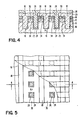
- FIG. 5 shows a top view of the surface of the section shown in FIG. 4.
- Fig. 4 shows the section 4-4, which emerges from Fig. 5.
- FIGS. 4, 5 The operation of a circuit structure according to FIGS. 4, 5 can be better described in connection with FIGS. 4, 5 and 6.
- a positive voltage is applied to word line 28 during a write operation.
- Channel 34 then becomes conductive.
- the writing of a binary 1 or a 0 is determined by the voltage on the bit line, which takes a high or a low level value. These levels are used to control whether or not electrical charges are stored in the potential well 25, which well is formed in the P - doped substrate near the thin gate oxide 24, as well as in the operation of a charge coupled storage device (CCD) is the case.
- CCD charge coupled storage device
- the word line voltage drops back to its quiescent level, thereby screening the channel before the bit line returns to its quiescent state.
- the quiescent voltage of the word line should be high enough to maintain the potential wells of these memory cells.
- the word line voltage drops, typically to 0 volts. This reduces the surface potential and the charges that were originally stored in the potential wells flow outwards onto the bit lines and are sensed.
- the bit line is kept at a positive voltage. Details of the memory cell operation described above are described in AF Tasch's article "The Charge-Coupled RAM Cell Concept", which is in the IEEE Journal of Solid-State Circuits, Vol. SC-11, No. 1, February 1976, on pages 58 until 63 is published.
- FIGS. 7 to 14 A second embodiment is shown in FIGS. 7 to 14. This embodiment is preferable because it results in a MOSFET structure for random access memory that realizes vertical one-channel FETs that are realized on the side surfaces of the trenches.
- This random access memory is about half the size of previously known random access VMOSFET memory.
- the capacity ratio of memory to bit line remains approximately the same despite this size reduction.
- the structure consists of a monocrystalline silicon substrate 60, which may have any crystallographic orientation of an overlying N + layer 61, one above the N + - lying doped layer p-doped layer 62 and a second N + - doped layer 63, the lies over the P-conducting layer.
- the P + doped substrate may have a conductivity of 1 X 10 18 atoms / cm 3 or more.
- the layers 61, 62 and 63 can be formed with the aid of conventional epitaxial growth techniques, that is to say those processes which have already been explained in connection with FIGS. 1 to 5.
- the rows of layers can also be formed using combinations between epitaxial growth and / or unmasked diffusion steps.
- the conductivity of layer 61 which is preferred here, is 10 20 atoms / cm 3 .
- the conductivity of the P-doped layer 62 is chosen with 1 x 10 16 to 1 x 10¹⁷ atoms / cm 3 and that of the N + -doped layer 63 with 1020 atoms / cm3.
- U-shaped openings are made in the semiconductor body by driving the etching through a suitable pattern of a mask layer into the P + -doped substrate 60.
- the result of this process step is a pattern of openings, the areas monocrystalline Isolate a silicon substrate and the overlying layers from each other.
- the resulting openings in the pattern are then filled with dielectric material such as silicon dioxide, silicon nitride, aluminum trioxide and / or combinations of these materials. These filled openings are then viewed as dielectric isolation regions 64.
- the dielectric material is also deposited on the surface of the semiconductor body as layer 65.
- This layer 65 is completely removed from the N + -doped layer 63 by reactive ion etching.
- the result of this reactive ion etching is the N + islands on the surface of the dielectric silicon dioxide filler layer 64.
- a layer 66 of highly doped N + polycrystalline silicon is then applied over the entire surface, so that a structure has now been created which is shown in FIG. 9 shows.
- a second reactive ion etch is performed which drives deep openings and trenches 20 through the dielectric layer 68 and layers 66, 63, 62 and 61 into the P + - conductive substrate 60.
- the process for forming the opening 70 by means of reactive ion etching has already been explained in connection with FR-A-7 610 361 mentioned at the beginning and in connection with the first exemplary embodiment in FIG. 3.
- the resulting opening is essentially U-shaped with a slight bevel from the vertical and preferably 2 ° to 10 °.
- the regions of monocrystalline silicon between the dielectric insulation regions 64 are essentially halved by U-shaped openings 70.
- the openings 70 isolate the halved regions of monocrystalline silicon from one another, since they extend from one dielectric region to the next.
- the silicon dioxide insulator 72 for a gate is formed by exposing the semiconductor body to an oxidation atmosphere of, for example, 970 ° C. in oxygen or water vapor.
- the thickness of this gate dielectric can be, for example, between approximately 400 and 1000 angstroms.
- the dimensions of the gate, along with other critical dimensions of the circuit, can be changed in accordance with the scale rules for MOSFETs described in the design of ion-implanted MOSFETs With Very Small Physical Dimensions by RH Dennard, et alita in IEEE J. Solid -State Circuits Vol. SC-9, No. 5, pages 256 to 268, October 1974. The result of this process is the structure shown in FIG. 11.
- the doped polycrystalline layer 74 typically produced by chemical vapor deposition, as has already been explained in connection with FIG. 4, is deposited in the openings 70 which contain the gate dielectric 72 and over the entire surface of the silicon dioxide layer 68
- the doped polycrystalline silicon within the openings acts like a gate connection 75.
- the desired pattern of word lines is now applied photolithographically to the surface layer of the polycrystalline N + -doped silicon which is preferably used.
- Passivation layers are now applied to the entire structure, which shield the integrated circuit against contamination of the ambient atmosphere. These passivation coatings are applied using known methods.
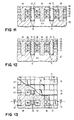
- FIG. 13 shows a top view of the structure of the integrated circuit with the surface layer partially removed.
- Fig. 12 shows a section along the line 12-12 in Fig. 13.
- the polycrystalline N + -doped silicon layer 66 represents the bit line of the memory.
- the N + -doped layers 61 and 63 are the source / drain regions of the MOSFET.
- the P-type layer 62 separates the N + -doped layers 61 and 63 from each other and provides the area for the MOSFET channel.
- the connection between the P + -doped substrate 60 and the N + -doped layer 61 forms the capacitor of the memory cell.
- Fig. 14 shows the electrical concerns of the embodiments shown in Figs. 12 and 13.
- the same reference numerals in FIGS. 12, 13 and 14 also show the same concrete elements.
- Bit lines 66 connect the memory cell to the sense amplifier and word lines 74 to the word drivers.
- the memory cell is basically a dynamic one-element cell as described in US-A-3 387 286.
- FIGS. 12 and 13 The mode of operation of the exemplary embodiments in FIGS. 12 and 13 is explained in more detail below with reference to FIG. 14.
- the operation of these memory cells is very similar to that in the aforementioned US Pat. No. 3,387,286.
- a positive voltage is applied to word line 74 which makes channel 72 conductive.
- the writing of a binary 1 or a binary 0 is determined by the voltage on the bit line 66, which must assume a high signal level for a binary 1 and a low signal level for a binary 0.
- the voltage on the word line drops to the quiescent level and also switches off the channel before the voltage on the bit line also drops to its quiescent level.
- the voltage on the word line rises again and also switches the channel on, so that the charges stored in the capacitor flow back over the bit line and can be sensed there.
Landscapes
- Engineering & Computer Science (AREA)
- Computer Hardware Design (AREA)
- Microelectronics & Electronic Packaging (AREA)
- Manufacturing & Machinery (AREA)
- Semiconductor Memories (AREA)
- Local Oxidation Of Silicon (AREA)
- Element Separation (AREA)
Applications Claiming Priority (2)
| Application Number | Priority Date | Filing Date | Title |
|---|---|---|---|
| US06/036,722 US4252579A (en) | 1979-05-07 | 1979-05-07 | Method for making single electrode U-MOSFET random access memory utilizing reactive ion etching and polycrystalline deposition |
| US36722 | 1979-05-07 |
Publications (2)
| Publication Number | Publication Date |
|---|---|
| EP0018501A1 EP0018501A1 (de) | 1980-11-12 |
| EP0018501B1 true EP0018501B1 (de) | 1983-05-25 |
Family
ID=21890246
Family Applications (1)
| Application Number | Title | Priority Date | Filing Date |
|---|---|---|---|
| EP80101629A Expired EP0018501B1 (de) | 1979-05-07 | 1980-03-27 | Verfahren zur Herstellung von hochverdichteten vertikalen FETs und eine daraus gebildete Matrixanordnung |
Country Status (6)
| Country | Link |
|---|---|
| US (1) | US4252579A (it) |
| EP (1) | EP0018501B1 (it) |
| JP (1) | JPS5840343B2 (it) |
| CA (1) | CA1133136A (it) |
| DE (1) | DE3063421D1 (it) |
| IT (1) | IT1149830B (it) |
Families Citing this family (53)
| Publication number | Priority date | Publication date | Assignee | Title |
|---|---|---|---|---|
| JPS5827667B2 (ja) * | 1979-02-19 | 1983-06-10 | 富士通株式会社 | 半導体装置 |
| JPS5636143A (en) * | 1979-08-31 | 1981-04-09 | Hitachi Ltd | Manufacture of semiconductor device |
| US4333227A (en) * | 1979-11-29 | 1982-06-08 | International Business Machines Corporation | Process for fabricating a self-aligned micrometer bipolar transistor device |
| US4400715A (en) * | 1980-11-19 | 1983-08-23 | International Business Machines Corporation | Thin film semiconductor device and method for manufacture |
| US4333794A (en) * | 1981-04-07 | 1982-06-08 | International Business Machines Corporation | Omission of thick Si3 N4 layers in ISA schemes |
| GB2104722B (en) * | 1981-06-25 | 1985-04-24 | Suwa Seikosha Kk | Mos semiconductor device and method of manufacturing the same |
| JPS583248A (ja) * | 1981-06-30 | 1983-01-10 | Toshiba Corp | バイポ−ラ型半導体装置の製造方法 |
| US4375124A (en) * | 1981-11-12 | 1983-03-01 | Gte Laboratories Incorporated | Power static induction transistor fabrication |
| US4554570A (en) * | 1982-06-24 | 1985-11-19 | Rca Corporation | Vertically integrated IGFET device |
| JPS5982761A (ja) * | 1982-11-04 | 1984-05-12 | Hitachi Ltd | 半導体メモリ |
| US4830975A (en) * | 1983-01-13 | 1989-05-16 | National Semiconductor Corporation | Method of manufacture a primos device |
| JPH0666436B2 (ja) * | 1983-04-15 | 1994-08-24 | 株式会社日立製作所 | 半導体集積回路装置 |
| JPS6070766A (ja) * | 1983-09-26 | 1985-04-22 | Mitsubishi Electric Corp | 半導体装置の製造方法 |
| JPS60128654A (ja) * | 1983-12-16 | 1985-07-09 | Hitachi Ltd | 半導体集積回路 |
| JPH0793365B2 (ja) * | 1984-09-11 | 1995-10-09 | 株式会社東芝 | 半導体記憶装置およびその製造方法 |
| US4916511A (en) * | 1985-05-03 | 1990-04-10 | Texas Instruments Incorporated | Trench structure and process |
| US4855017A (en) * | 1985-05-03 | 1989-08-08 | Texas Instruments Incorporated | Trench etch process for a single-wafer RIE dry etch reactor |
| US4788158A (en) * | 1985-09-25 | 1988-11-29 | Texas Instruments Incorporated | Method of making vertical inverter |
| US4937648A (en) * | 1986-03-12 | 1990-06-26 | Huang Jack S T | Resistant transistor |
| NL8600786A (nl) * | 1986-03-27 | 1987-10-16 | Philips Nv | Ladingsgekoppelde inrichting. |
| US4829017A (en) * | 1986-09-25 | 1989-05-09 | Texas Instruments Incorporated | Method for lubricating a high capacity dram cell |
| JPS6370851U (it) * | 1986-10-28 | 1988-05-12 | ||
| US5082795A (en) * | 1986-12-05 | 1992-01-21 | General Electric Company | Method of fabricating a field effect semiconductor device having a self-aligned structure |
| US4794561A (en) * | 1987-07-02 | 1988-12-27 | Integrated Device Technology, Inc. | Static ram cell with trench pull-down transistors and buried-layer ground plate |
| US5545290A (en) * | 1987-07-09 | 1996-08-13 | Texas Instruments Incorporated | Etching method |
| US5164325A (en) * | 1987-10-08 | 1992-11-17 | Siliconix Incorporated | Method of making a vertical current flow field effect transistor |
| US5015594A (en) * | 1988-10-24 | 1991-05-14 | International Business Machines Corporation | Process of making BiCMOS devices having closely spaced device regions |
| US4894697A (en) * | 1988-10-31 | 1990-01-16 | International Business Machines Corporation | Ultra dense dram cell and its method of fabrication |
| US5028980A (en) * | 1988-12-21 | 1991-07-02 | Texas Instruments Incorporated | Trench capacitor with expanded area |
| US5064777A (en) * | 1990-06-28 | 1991-11-12 | International Business Machines Corporation | Fabrication method for a double trench memory cell device |
| US5192708A (en) * | 1991-04-29 | 1993-03-09 | International Business Machines Corporation | Sub-layer contact technique using in situ doped amorphous silicon and solid phase recrystallization |
| US5395784A (en) * | 1993-04-14 | 1995-03-07 | Industrial Technology Research Institute | Method of manufacturing low leakage and long retention time DRAM |
| KR0123751B1 (ko) * | 1993-10-07 | 1997-11-25 | 김광호 | 반도체장치 및 그 제조방법 |
| US6150687A (en) | 1997-07-08 | 2000-11-21 | Micron Technology, Inc. | Memory cell having a vertical transistor with buried source/drain and dual gates |
| US6072209A (en) | 1997-07-08 | 2000-06-06 | Micro Technology, Inc. | Four F2 folded bit line DRAM cell structure having buried bit and word lines |
| US5909618A (en) | 1997-07-08 | 1999-06-01 | Micron Technology, Inc. | Method of making memory cell with vertical transistor and buried word and body lines |
| US5973356A (en) * | 1997-07-08 | 1999-10-26 | Micron Technology, Inc. | Ultra high density flash memory |
| US5907170A (en) | 1997-10-06 | 1999-05-25 | Micron Technology, Inc. | Circuit and method for an open bit line memory cell with a vertical transistor and trench plate trench capacitor |
| US6066869A (en) * | 1997-10-06 | 2000-05-23 | Micron Technology, Inc. | Circuit and method for a folded bit line memory cell with vertical transistor and trench capacitor |
| US6528837B2 (en) | 1997-10-06 | 2003-03-04 | Micron Technology, Inc. | Circuit and method for an open bit line memory cell with a vertical transistor and trench plate trench capacitor |
| KR100275727B1 (ko) * | 1998-01-06 | 2001-01-15 | 윤종용 | 반도체 장치의 커패시터 형성방법 |
| US6025225A (en) * | 1998-01-22 | 2000-02-15 | Micron Technology, Inc. | Circuits with a trench capacitor having micro-roughened semiconductor surfaces and methods for forming the same |
| US6246083B1 (en) | 1998-02-24 | 2001-06-12 | Micron Technology, Inc. | Vertical gain cell and array for a dynamic random access memory |
| US5991225A (en) * | 1998-02-27 | 1999-11-23 | Micron Technology, Inc. | Programmable memory address decode array with vertical transistors |
| US6124729A (en) | 1998-02-27 | 2000-09-26 | Micron Technology, Inc. | Field programmable logic arrays with vertical transistors |
| US6043527A (en) | 1998-04-14 | 2000-03-28 | Micron Technology, Inc. | Circuits and methods for a memory cell with a trench plate trench capacitor and a vertical bipolar read device |
| US6208164B1 (en) | 1998-08-04 | 2001-03-27 | Micron Technology, Inc. | Programmable logic array with vertical transistors |
| US6134175A (en) | 1998-08-04 | 2000-10-17 | Micron Technology, Inc. | Memory address decode array with vertical transistors |
| US7229872B2 (en) * | 2000-04-04 | 2007-06-12 | International Rectifier Corporation | Low voltage power MOSFET device and process for its manufacture |
| SG112804A1 (en) * | 2001-05-10 | 2005-07-28 | Inst Of Microelectronics | Sloped trench etching process |
| JP2007189008A (ja) * | 2006-01-12 | 2007-07-26 | Elpida Memory Inc | 半導体記憶装置およびその製造方法 |
| US10361200B1 (en) | 2018-03-07 | 2019-07-23 | International Business Machines Corporation | Vertical fin field effect transistor with integral U-shaped electrical gate connection |
| US20230292497A1 (en) * | 2022-03-11 | 2023-09-14 | Nanya Technology Corporation | Manufacturing method of semiconductor structure |
Family Cites Families (17)
| Publication number | Priority date | Publication date | Assignee | Title |
|---|---|---|---|---|
| US3412297A (en) * | 1965-12-16 | 1968-11-19 | United Aircraft Corp | Mos field-effect transistor with a onemicron vertical channel |
| US4017883A (en) * | 1971-07-06 | 1977-04-12 | Ibm Corporation | Single-electrode charge-coupled random access memory cell with impurity implanted gate region |
| US3938241A (en) * | 1972-10-24 | 1976-02-17 | Motorola, Inc. | Vertical channel junction field-effect transistors and method of manufacture |
| NL157137B (nl) * | 1973-03-27 | 1978-06-15 | Nkf Kabel Bv | Werkwijze en inrichting voor het gelijkmatig met poedervormig materiaal bedekken van een langwerpig voorwerp, waarvan althans de buitenlaag bestaat uit door warmte smeltbare kunststof. |
| US3975221A (en) * | 1973-08-29 | 1976-08-17 | American Micro-Systems, Inc. | Low capacitance V groove MOS NOR gate and method of manufacture |
| US4003126A (en) * | 1974-09-12 | 1977-01-18 | Canadian Patents And Development Limited | Method of making metal oxide semiconductor devices |
| US4037306A (en) * | 1975-10-02 | 1977-07-26 | Motorola, Inc. | Integrated circuit and method |
| US4003036A (en) * | 1975-10-23 | 1977-01-11 | American Micro-Systems, Inc. | Single IGFET memory cell with buried storage element |
| US4222062A (en) * | 1976-05-04 | 1980-09-09 | American Microsystems, Inc. | VMOS Floating gate memory device |
| US4070690A (en) * | 1976-08-17 | 1978-01-24 | Westinghouse Electric Corporation | VMOS transistor |
| DE2642615C2 (de) * | 1976-09-22 | 1986-04-24 | Siemens AG, 1000 Berlin und 8000 München | Halbleiterspeicher |
| US4084175A (en) * | 1976-09-30 | 1978-04-11 | Research Corporation | Double implanted planar mos device with v-groove and process of manufacture thereof |
| US4044452A (en) * | 1976-10-06 | 1977-08-30 | International Business Machines Corporation | Process for making field effect and bipolar transistors on the same semiconductor chip |
| US4145703A (en) * | 1977-04-15 | 1979-03-20 | Supertex, Inc. | High power MOS device and fabrication method therefor |
| US4104086A (en) * | 1977-08-15 | 1978-08-01 | International Business Machines Corporation | Method for forming isolated regions of silicon utilizing reactive ion etching |
| CA1118892A (en) * | 1977-12-27 | 1982-02-23 | John R. Edwards | Semiconductor device utilizing memory cells with sidewall charge storage regions |
| US4116720A (en) * | 1977-12-27 | 1978-09-26 | Burroughs Corporation | Method of making a V-MOS field effect transistor for a dynamic memory cell having improved capacitance |
-
1979
- 1979-05-07 US US06/036,722 patent/US4252579A/en not_active Expired - Lifetime
-
1980
- 1980-02-20 JP JP55019308A patent/JPS5840343B2/ja not_active Expired
- 1980-03-21 CA CA348,131A patent/CA1133136A/en not_active Expired
- 1980-03-27 EP EP80101629A patent/EP0018501B1/de not_active Expired
- 1980-03-27 DE DE8080101629T patent/DE3063421D1/de not_active Expired
- 1980-04-11 IT IT21316/80A patent/IT1149830B/it active
Non-Patent Citations (1)
| Title |
|---|
| IBM TECHICAL DISCLOSURE BULLETIN, Band 21, Nr. 7, Dezember 1978, New York, US, F. BARSON: "Dynamic DMOS-random-access memory cell design with trench", Seiten 2755-2756 * |
Also Published As
| Publication number | Publication date |
|---|---|
| CA1133136A (en) | 1982-10-05 |
| DE3063421D1 (en) | 1983-07-07 |
| IT8021316A0 (it) | 1980-04-11 |
| EP0018501A1 (de) | 1980-11-12 |
| JPS5840343B2 (ja) | 1983-09-05 |
| JPS55148438A (en) | 1980-11-19 |
| US4252579A (en) | 1981-02-24 |
| IT1149830B (it) | 1986-12-10 |
Similar Documents
| Publication | Publication Date | Title |
|---|---|---|
| EP0018501B1 (de) | Verfahren zur Herstellung von hochverdichteten vertikalen FETs und eine daraus gebildete Matrixanordnung | |
| DE3880750T2 (de) | Vertikale Transistor-/Kapazitätspeicherzellen-Struktur und Herstellungsverfahren dafür. | |
| EP0002670B1 (de) | Verfahren zum Herstellen eines bipolaren Transistors in einem Halbleitersubstrat | |
| DE3788499T2 (de) | Halbleiter-Grabenkondensator-Struktur. | |
| EP0744771B1 (de) | Verfahren zur Herstellung einer DRAM-Speicherzelle mit vertikalem Transistor | |
| DE69130163T2 (de) | Verfahren zur Herstellung einer MOS-EEPROM-Transistorzelle mit schwebendem Gate | |
| DE3037431C2 (it) | ||
| DE19512431C2 (de) | Halbleiterspeicherzelle mit wahlfreiem Zugriff auf Silicium-auf-Isolator mit doppelten Steuergates und deren Herstellungsverfahren | |
| DE3780840T2 (de) | Einen rillenkondensator enthaltender dynamischer speicher mit wahlfreiem zugriff. | |
| DE2502235C2 (it) | ||
| DE4215708C2 (de) | SRAM und Verfahren zu dessen Herstellung | |
| DE3787687T2 (de) | Halbleiterspeicher. | |
| DE3525418A1 (de) | Halbleiterspeichereinrichtung und verfahren zu ihrer herstellung | |
| DE3844388A1 (de) | Dynamische direktzugriffspeichereinrichtung | |
| DE3916228A1 (de) | Halbleiterspeichervorrichtung mit stapelkondensatorzellenstruktur und verfahren zu ihrer herstellung | |
| EP0875937A2 (de) | DRAM-Zellenanordnung und Verfahren zu deren Herstellung | |
| DE19941148A1 (de) | Speicher mit Grabenkondensator und Auswahltransistor und Verfahren zu seiner Herstellung | |
| DE3530773A1 (de) | Halbleitervorrichtung und verfahren zu ihrer herstellung | |
| DE2328090A1 (de) | Halbleiterkondensator mit grosser kapazitaet und verfahren zu seiner herstellung | |
| EP0317934B1 (de) | Dreidimensionale 1-Transistorzellenanordnung für dynamische Halbleiterspeicher mit Grabenkondensator und Verfahren zu ihrer Herstellung | |
| EP1125328B1 (de) | Verfahren zur herstellung einer dram-zellenanordnung | |
| DE10022696A1 (de) | Herstellungsverfahren einer Halbleitereinrichtung und Halbleitereinrichtung | |
| EP1282917B1 (de) | Vertikaler transistor | |
| EP0989603A2 (de) | Grabenkondesator mit Isolationskragen und entsprechendes Herstellungsverfahren | |
| DE19646419C1 (de) | Verfahren zur Herstellung einer elektrisch schreib- und löschbaren Festwertspeicherzellenanordnung |
Legal Events
| Date | Code | Title | Description |
|---|---|---|---|
| PUAI | Public reference made under article 153(3) epc to a published international application that has entered the european phase |
Free format text: ORIGINAL CODE: 0009012 |
|
| AK | Designated contracting states |
Designated state(s): DE FR GB |
|
| 17P | Request for examination filed |
Effective date: 19810312 |
|
| GRAA | (expected) grant |
Free format text: ORIGINAL CODE: 0009210 |
|
| AK | Designated contracting states |
Designated state(s): DE FR GB |
|
| REF | Corresponds to: |
Ref document number: 3063421 Country of ref document: DE Date of ref document: 19830707 |
|
| ET | Fr: translation filed | ||
| PLBE | No opposition filed within time limit |
Free format text: ORIGINAL CODE: 0009261 |
|
| STAA | Information on the status of an ep patent application or granted ep patent |
Free format text: STATUS: NO OPPOSITION FILED WITHIN TIME LIMIT |
|
| 26N | No opposition filed | ||
| PGFP | Annual fee paid to national office [announced via postgrant information from national office to epo] |
Ref country code: GB Payment date: 19910220 Year of fee payment: 12 |
|
| PGFP | Annual fee paid to national office [announced via postgrant information from national office to epo] |
Ref country code: FR Payment date: 19910225 Year of fee payment: 12 |
|
| PGFP | Annual fee paid to national office [announced via postgrant information from national office to epo] |
Ref country code: DE Payment date: 19910323 Year of fee payment: 12 |
|
| PG25 | Lapsed in a contracting state [announced via postgrant information from national office to epo] |
Ref country code: GB Effective date: 19920327 |
|
| GBPC | Gb: european patent ceased through non-payment of renewal fee | ||
| PG25 | Lapsed in a contracting state [announced via postgrant information from national office to epo] |
Ref country code: FR Effective date: 19921130 |
|
| PG25 | Lapsed in a contracting state [announced via postgrant information from national office to epo] |
Ref country code: DE Effective date: 19921201 |
|
| REG | Reference to a national code |
Ref country code: FR Ref legal event code: ST |