CN108563366B - Touch screen liquid crystal display - Google Patents
Touch screen liquid crystal display Download PDFInfo
- Publication number
- CN108563366B CN108563366B CN201810604129.1A CN201810604129A CN108563366B CN 108563366 B CN108563366 B CN 108563366B CN 201810604129 A CN201810604129 A CN 201810604129A CN 108563366 B CN108563366 B CN 108563366B
- Authority
- CN
- China
- Prior art keywords
- touch
- display
- electrodes
- touch screen
- lcd
- Prior art date
- Legal status (The legal status is an assumption and is not a legal conclusion. Google has not performed a legal analysis and makes no representation as to the accuracy of the status listed.)
- Active
Links
Images


Classifications
-
- G—PHYSICS
- G06—COMPUTING; CALCULATING OR COUNTING
- G06F—ELECTRIC DIGITAL DATA PROCESSING
- G06F3/00—Input arrangements for transferring data to be processed into a form capable of being handled by the computer; Output arrangements for transferring data from processing unit to output unit, e.g. interface arrangements
- G06F3/01—Input arrangements or combined input and output arrangements for interaction between user and computer
- G06F3/03—Arrangements for converting the position or the displacement of a member into a coded form
- G06F3/041—Digitisers, e.g. for touch screens or touch pads, characterised by the transducing means
- G06F3/0416—Control or interface arrangements specially adapted for digitisers
-
- G—PHYSICS
- G02—OPTICS
- G02F—OPTICAL DEVICES OR ARRANGEMENTS FOR THE CONTROL OF LIGHT BY MODIFICATION OF THE OPTICAL PROPERTIES OF THE MEDIA OF THE ELEMENTS INVOLVED THEREIN; NON-LINEAR OPTICS; FREQUENCY-CHANGING OF LIGHT; OPTICAL LOGIC ELEMENTS; OPTICAL ANALOGUE/DIGITAL CONVERTERS
- G02F1/00—Devices or arrangements for the control of the intensity, colour, phase, polarisation or direction of light arriving from an independent light source, e.g. switching, gating or modulating; Non-linear optics
- G02F1/01—Devices or arrangements for the control of the intensity, colour, phase, polarisation or direction of light arriving from an independent light source, e.g. switching, gating or modulating; Non-linear optics for the control of the intensity, phase, polarisation or colour
- G02F1/13—Devices or arrangements for the control of the intensity, colour, phase, polarisation or direction of light arriving from an independent light source, e.g. switching, gating or modulating; Non-linear optics for the control of the intensity, phase, polarisation or colour based on liquid crystals, e.g. single liquid crystal display cells
- G02F1/133—Constructional arrangements; Operation of liquid crystal cells; Circuit arrangements
- G02F1/1333—Constructional arrangements; Manufacturing methods
- G02F1/13338—Input devices, e.g. touch panels
-
- G—PHYSICS
- G06—COMPUTING; CALCULATING OR COUNTING
- G06F—ELECTRIC DIGITAL DATA PROCESSING
- G06F3/00—Input arrangements for transferring data to be processed into a form capable of being handled by the computer; Output arrangements for transferring data from processing unit to output unit, e.g. interface arrangements
- G06F3/01—Input arrangements or combined input and output arrangements for interaction between user and computer
- G06F3/03—Arrangements for converting the position or the displacement of a member into a coded form
- G06F3/041—Digitisers, e.g. for touch screens or touch pads, characterised by the transducing means
- G06F3/0412—Digitisers structurally integrated in a display
-
- G—PHYSICS
- G02—OPTICS
- G02F—OPTICAL DEVICES OR ARRANGEMENTS FOR THE CONTROL OF LIGHT BY MODIFICATION OF THE OPTICAL PROPERTIES OF THE MEDIA OF THE ELEMENTS INVOLVED THEREIN; NON-LINEAR OPTICS; FREQUENCY-CHANGING OF LIGHT; OPTICAL LOGIC ELEMENTS; OPTICAL ANALOGUE/DIGITAL CONVERTERS
- G02F1/00—Devices or arrangements for the control of the intensity, colour, phase, polarisation or direction of light arriving from an independent light source, e.g. switching, gating or modulating; Non-linear optics
- G02F1/01—Devices or arrangements for the control of the intensity, colour, phase, polarisation or direction of light arriving from an independent light source, e.g. switching, gating or modulating; Non-linear optics for the control of the intensity, phase, polarisation or colour
- G02F1/13—Devices or arrangements for the control of the intensity, colour, phase, polarisation or direction of light arriving from an independent light source, e.g. switching, gating or modulating; Non-linear optics for the control of the intensity, phase, polarisation or colour based on liquid crystals, e.g. single liquid crystal display cells
- G02F1/133—Constructional arrangements; Operation of liquid crystal cells; Circuit arrangements
- G02F1/1333—Constructional arrangements; Manufacturing methods
- G02F1/1335—Structural association of cells with optical devices, e.g. polarisers or reflectors
- G02F1/133509—Filters, e.g. light shielding masks
- G02F1/133514—Colour filters
-
- G—PHYSICS
- G02—OPTICS
- G02F—OPTICAL DEVICES OR ARRANGEMENTS FOR THE CONTROL OF LIGHT BY MODIFICATION OF THE OPTICAL PROPERTIES OF THE MEDIA OF THE ELEMENTS INVOLVED THEREIN; NON-LINEAR OPTICS; FREQUENCY-CHANGING OF LIGHT; OPTICAL LOGIC ELEMENTS; OPTICAL ANALOGUE/DIGITAL CONVERTERS
- G02F1/00—Devices or arrangements for the control of the intensity, colour, phase, polarisation or direction of light arriving from an independent light source, e.g. switching, gating or modulating; Non-linear optics
- G02F1/01—Devices or arrangements for the control of the intensity, colour, phase, polarisation or direction of light arriving from an independent light source, e.g. switching, gating or modulating; Non-linear optics for the control of the intensity, phase, polarisation or colour
- G02F1/13—Devices or arrangements for the control of the intensity, colour, phase, polarisation or direction of light arriving from an independent light source, e.g. switching, gating or modulating; Non-linear optics for the control of the intensity, phase, polarisation or colour based on liquid crystals, e.g. single liquid crystal display cells
- G02F1/133—Constructional arrangements; Operation of liquid crystal cells; Circuit arrangements
- G02F1/1333—Constructional arrangements; Manufacturing methods
- G02F1/1335—Structural association of cells with optical devices, e.g. polarisers or reflectors
- G02F1/133528—Polarisers
-
- G—PHYSICS
- G02—OPTICS
- G02F—OPTICAL DEVICES OR ARRANGEMENTS FOR THE CONTROL OF LIGHT BY MODIFICATION OF THE OPTICAL PROPERTIES OF THE MEDIA OF THE ELEMENTS INVOLVED THEREIN; NON-LINEAR OPTICS; FREQUENCY-CHANGING OF LIGHT; OPTICAL LOGIC ELEMENTS; OPTICAL ANALOGUE/DIGITAL CONVERTERS
- G02F1/00—Devices or arrangements for the control of the intensity, colour, phase, polarisation or direction of light arriving from an independent light source, e.g. switching, gating or modulating; Non-linear optics
- G02F1/01—Devices or arrangements for the control of the intensity, colour, phase, polarisation or direction of light arriving from an independent light source, e.g. switching, gating or modulating; Non-linear optics for the control of the intensity, phase, polarisation or colour
- G02F1/13—Devices or arrangements for the control of the intensity, colour, phase, polarisation or direction of light arriving from an independent light source, e.g. switching, gating or modulating; Non-linear optics for the control of the intensity, phase, polarisation or colour based on liquid crystals, e.g. single liquid crystal display cells
- G02F1/133—Constructional arrangements; Operation of liquid crystal cells; Circuit arrangements
- G02F1/1333—Constructional arrangements; Manufacturing methods
- G02F1/1343—Electrodes
- G02F1/134309—Electrodes characterised by their geometrical arrangement
- G02F1/134363—Electrodes characterised by their geometrical arrangement for applying an electric field parallel to the substrate, i.e. in-plane switching [IPS]
-
- G—PHYSICS
- G02—OPTICS
- G02F—OPTICAL DEVICES OR ARRANGEMENTS FOR THE CONTROL OF LIGHT BY MODIFICATION OF THE OPTICAL PROPERTIES OF THE MEDIA OF THE ELEMENTS INVOLVED THEREIN; NON-LINEAR OPTICS; FREQUENCY-CHANGING OF LIGHT; OPTICAL LOGIC ELEMENTS; OPTICAL ANALOGUE/DIGITAL CONVERTERS
- G02F1/00—Devices or arrangements for the control of the intensity, colour, phase, polarisation or direction of light arriving from an independent light source, e.g. switching, gating or modulating; Non-linear optics
- G02F1/01—Devices or arrangements for the control of the intensity, colour, phase, polarisation or direction of light arriving from an independent light source, e.g. switching, gating or modulating; Non-linear optics for the control of the intensity, phase, polarisation or colour
- G02F1/13—Devices or arrangements for the control of the intensity, colour, phase, polarisation or direction of light arriving from an independent light source, e.g. switching, gating or modulating; Non-linear optics for the control of the intensity, phase, polarisation or colour based on liquid crystals, e.g. single liquid crystal display cells
- G02F1/133—Constructional arrangements; Operation of liquid crystal cells; Circuit arrangements
- G02F1/136—Liquid crystal cells structurally associated with a semi-conducting layer or substrate, e.g. cells forming part of an integrated circuit
- G02F1/1362—Active matrix addressed cells
-
- G—PHYSICS
- G06—COMPUTING; CALCULATING OR COUNTING
- G06F—ELECTRIC DIGITAL DATA PROCESSING
- G06F3/00—Input arrangements for transferring data to be processed into a form capable of being handled by the computer; Output arrangements for transferring data from processing unit to output unit, e.g. interface arrangements
- G06F3/01—Input arrangements or combined input and output arrangements for interaction between user and computer
- G06F3/03—Arrangements for converting the position or the displacement of a member into a coded form
- G06F3/041—Digitisers, e.g. for touch screens or touch pads, characterised by the transducing means
- G06F3/0416—Control or interface arrangements specially adapted for digitisers
- G06F3/04166—Details of scanning methods, e.g. sampling time, grouping of sub areas or time sharing with display driving
-
- G—PHYSICS
- G06—COMPUTING; CALCULATING OR COUNTING
- G06F—ELECTRIC DIGITAL DATA PROCESSING
- G06F3/00—Input arrangements for transferring data to be processed into a form capable of being handled by the computer; Output arrangements for transferring data from processing unit to output unit, e.g. interface arrangements
- G06F3/01—Input arrangements or combined input and output arrangements for interaction between user and computer
- G06F3/03—Arrangements for converting the position or the displacement of a member into a coded form
- G06F3/041—Digitisers, e.g. for touch screens or touch pads, characterised by the transducing means
- G06F3/0416—Control or interface arrangements specially adapted for digitisers
- G06F3/0418—Control or interface arrangements specially adapted for digitisers for error correction or compensation, e.g. based on parallax, calibration or alignment
- G06F3/04184—Synchronisation with the driving of the display or the backlighting unit to avoid interferences generated internally
-
- G—PHYSICS
- G06—COMPUTING; CALCULATING OR COUNTING
- G06F—ELECTRIC DIGITAL DATA PROCESSING
- G06F3/00—Input arrangements for transferring data to be processed into a form capable of being handled by the computer; Output arrangements for transferring data from processing unit to output unit, e.g. interface arrangements
- G06F3/01—Input arrangements or combined input and output arrangements for interaction between user and computer
- G06F3/03—Arrangements for converting the position or the displacement of a member into a coded form
- G06F3/041—Digitisers, e.g. for touch screens or touch pads, characterised by the transducing means
- G06F3/044—Digitisers, e.g. for touch screens or touch pads, characterised by the transducing means by capacitive means
- G06F3/0443—Digitisers, e.g. for touch screens or touch pads, characterised by the transducing means by capacitive means using a single layer of sensing electrodes
-
- G—PHYSICS
- G06—COMPUTING; CALCULATING OR COUNTING
- G06F—ELECTRIC DIGITAL DATA PROCESSING
- G06F3/00—Input arrangements for transferring data to be processed into a form capable of being handled by the computer; Output arrangements for transferring data from processing unit to output unit, e.g. interface arrangements
- G06F3/01—Input arrangements or combined input and output arrangements for interaction between user and computer
- G06F3/03—Arrangements for converting the position or the displacement of a member into a coded form
- G06F3/041—Digitisers, e.g. for touch screens or touch pads, characterised by the transducing means
- G06F3/044—Digitisers, e.g. for touch screens or touch pads, characterised by the transducing means by capacitive means
- G06F3/0444—Digitisers, e.g. for touch screens or touch pads, characterised by the transducing means by capacitive means using a single conductive element covering the whole sensing surface, e.g. by sensing the electrical current flowing at the corners
-
- G—PHYSICS
- G06—COMPUTING; CALCULATING OR COUNTING
- G06F—ELECTRIC DIGITAL DATA PROCESSING
- G06F3/00—Input arrangements for transferring data to be processed into a form capable of being handled by the computer; Output arrangements for transferring data from processing unit to output unit, e.g. interface arrangements
- G06F3/01—Input arrangements or combined input and output arrangements for interaction between user and computer
- G06F3/03—Arrangements for converting the position or the displacement of a member into a coded form
- G06F3/041—Digitisers, e.g. for touch screens or touch pads, characterised by the transducing means
- G06F3/044—Digitisers, e.g. for touch screens or touch pads, characterised by the transducing means by capacitive means
- G06F3/0445—Digitisers, e.g. for touch screens or touch pads, characterised by the transducing means by capacitive means using two or more layers of sensing electrodes, e.g. using two layers of electrodes separated by a dielectric layer
-
- G—PHYSICS
- G06—COMPUTING; CALCULATING OR COUNTING
- G06F—ELECTRIC DIGITAL DATA PROCESSING
- G06F3/00—Input arrangements for transferring data to be processed into a form capable of being handled by the computer; Output arrangements for transferring data from processing unit to output unit, e.g. interface arrangements
- G06F3/01—Input arrangements or combined input and output arrangements for interaction between user and computer
- G06F3/03—Arrangements for converting the position or the displacement of a member into a coded form
- G06F3/041—Digitisers, e.g. for touch screens or touch pads, characterised by the transducing means
- G06F3/044—Digitisers, e.g. for touch screens or touch pads, characterised by the transducing means by capacitive means
- G06F3/0446—Digitisers, e.g. for touch screens or touch pads, characterised by the transducing means by capacitive means using a grid-like structure of electrodes in at least two directions, e.g. using row and column electrodes
-
- G—PHYSICS
- G09—EDUCATION; CRYPTOGRAPHY; DISPLAY; ADVERTISING; SEALS
- G09G—ARRANGEMENTS OR CIRCUITS FOR CONTROL OF INDICATING DEVICES USING STATIC MEANS TO PRESENT VARIABLE INFORMATION
- G09G3/00—Control arrangements or circuits, of interest only in connection with visual indicators other than cathode-ray tubes
- G09G3/20—Control arrangements or circuits, of interest only in connection with visual indicators other than cathode-ray tubes for presentation of an assembly of a number of characters, e.g. a page, by composing the assembly by combination of individual elements arranged in a matrix no fixed position being assigned to or needed to be assigned to the individual characters or partial characters
- G09G3/34—Control arrangements or circuits, of interest only in connection with visual indicators other than cathode-ray tubes for presentation of an assembly of a number of characters, e.g. a page, by composing the assembly by combination of individual elements arranged in a matrix no fixed position being assigned to or needed to be assigned to the individual characters or partial characters by control of light from an independent source
- G09G3/36—Control arrangements or circuits, of interest only in connection with visual indicators other than cathode-ray tubes for presentation of an assembly of a number of characters, e.g. a page, by composing the assembly by combination of individual elements arranged in a matrix no fixed position being assigned to or needed to be assigned to the individual characters or partial characters by control of light from an independent source using liquid crystals
- G09G3/3611—Control of matrices with row and column drivers
- G09G3/3614—Control of polarity reversal in general
-
- G—PHYSICS
- G09—EDUCATION; CRYPTOGRAPHY; DISPLAY; ADVERTISING; SEALS
- G09G—ARRANGEMENTS OR CIRCUITS FOR CONTROL OF INDICATING DEVICES USING STATIC MEANS TO PRESENT VARIABLE INFORMATION
- G09G3/00—Control arrangements or circuits, of interest only in connection with visual indicators other than cathode-ray tubes
- G09G3/20—Control arrangements or circuits, of interest only in connection with visual indicators other than cathode-ray tubes for presentation of an assembly of a number of characters, e.g. a page, by composing the assembly by combination of individual elements arranged in a matrix no fixed position being assigned to or needed to be assigned to the individual characters or partial characters
- G09G3/34—Control arrangements or circuits, of interest only in connection with visual indicators other than cathode-ray tubes for presentation of an assembly of a number of characters, e.g. a page, by composing the assembly by combination of individual elements arranged in a matrix no fixed position being assigned to or needed to be assigned to the individual characters or partial characters by control of light from an independent source
- G09G3/36—Control arrangements or circuits, of interest only in connection with visual indicators other than cathode-ray tubes for presentation of an assembly of a number of characters, e.g. a page, by composing the assembly by combination of individual elements arranged in a matrix no fixed position being assigned to or needed to be assigned to the individual characters or partial characters by control of light from an independent source using liquid crystals
- G09G3/3611—Control of matrices with row and column drivers
- G09G3/3648—Control of matrices with row and column drivers using an active matrix
-
- G—PHYSICS
- G02—OPTICS
- G02F—OPTICAL DEVICES OR ARRANGEMENTS FOR THE CONTROL OF LIGHT BY MODIFICATION OF THE OPTICAL PROPERTIES OF THE MEDIA OF THE ELEMENTS INVOLVED THEREIN; NON-LINEAR OPTICS; FREQUENCY-CHANGING OF LIGHT; OPTICAL LOGIC ELEMENTS; OPTICAL ANALOGUE/DIGITAL CONVERTERS
- G02F2201/00—Constructional arrangements not provided for in groups G02F1/00 - G02F7/00
- G02F2201/12—Constructional arrangements not provided for in groups G02F1/00 - G02F7/00 electrode
- G02F2201/124—Constructional arrangements not provided for in groups G02F1/00 - G02F7/00 electrode interdigital
-
- G—PHYSICS
- G06—COMPUTING; CALCULATING OR COUNTING
- G06F—ELECTRIC DIGITAL DATA PROCESSING
- G06F2203/00—Indexing scheme relating to G06F3/00 - G06F3/048
- G06F2203/041—Indexing scheme relating to G06F3/041 - G06F3/045
- G06F2203/04103—Manufacturing, i.e. details related to manufacturing processes specially suited for touch sensitive devices
-
- G—PHYSICS
- G06—COMPUTING; CALCULATING OR COUNTING
- G06F—ELECTRIC DIGITAL DATA PROCESSING
- G06F2203/00—Indexing scheme relating to G06F3/00 - G06F3/048
- G06F2203/041—Indexing scheme relating to G06F3/041 - G06F3/045
- G06F2203/04104—Multi-touch detection in digitiser, i.e. details about the simultaneous detection of a plurality of touching locations, e.g. multiple fingers or pen and finger
-
- G—PHYSICS
- G06—COMPUTING; CALCULATING OR COUNTING
- G06F—ELECTRIC DIGITAL DATA PROCESSING
- G06F2203/00—Indexing scheme relating to G06F3/00 - G06F3/048
- G06F2203/041—Indexing scheme relating to G06F3/041 - G06F3/045
- G06F2203/04111—Cross over in capacitive digitiser, i.e. details of structures for connecting electrodes of the sensing pattern where the connections cross each other, e.g. bridge structures comprising an insulating layer, or vias through substrate
-
- G—PHYSICS
- G06—COMPUTING; CALCULATING OR COUNTING
- G06F—ELECTRIC DIGITAL DATA PROCESSING
- G06F2203/00—Indexing scheme relating to G06F3/00 - G06F3/048
- G06F2203/041—Indexing scheme relating to G06F3/041 - G06F3/045
- G06F2203/04112—Electrode mesh in capacitive digitiser: electrode for touch sensing is formed of a mesh of very fine, normally metallic, interconnected lines that are almost invisible to see. This provides a quite large but transparent electrode surface, without need for ITO or similar transparent conductive material
-
- G—PHYSICS
- G06—COMPUTING; CALCULATING OR COUNTING
- G06F—ELECTRIC DIGITAL DATA PROCESSING
- G06F3/00—Input arrangements for transferring data to be processed into a form capable of being handled by the computer; Output arrangements for transferring data from processing unit to output unit, e.g. interface arrangements
- G06F3/01—Input arrangements or combined input and output arrangements for interaction between user and computer
- G06F3/03—Arrangements for converting the position or the displacement of a member into a coded form
- G06F3/041—Digitisers, e.g. for touch screens or touch pads, characterised by the transducing means
- G06F3/0416—Control or interface arrangements specially adapted for digitisers
- G06F3/04164—Connections between sensors and controllers, e.g. routing lines between electrodes and connection pads
-
- G—PHYSICS
- G09—EDUCATION; CRYPTOGRAPHY; DISPLAY; ADVERTISING; SEALS
- G09G—ARRANGEMENTS OR CIRCUITS FOR CONTROL OF INDICATING DEVICES USING STATIC MEANS TO PRESENT VARIABLE INFORMATION
- G09G2300/00—Aspects of the constitution of display devices
- G09G2300/04—Structural and physical details of display devices
- G09G2300/0421—Structural details of the set of electrodes
- G09G2300/0426—Layout of electrodes and connections
-
- G—PHYSICS
- G09—EDUCATION; CRYPTOGRAPHY; DISPLAY; ADVERTISING; SEALS
- G09G—ARRANGEMENTS OR CIRCUITS FOR CONTROL OF INDICATING DEVICES USING STATIC MEANS TO PRESENT VARIABLE INFORMATION
- G09G2300/00—Aspects of the constitution of display devices
- G09G2300/04—Structural and physical details of display devices
- G09G2300/0439—Pixel structures
- G09G2300/0456—Pixel structures with a reflective area and a transmissive area combined in one pixel, such as in transflectance pixels
-
- G—PHYSICS
- G09—EDUCATION; CRYPTOGRAPHY; DISPLAY; ADVERTISING; SEALS
- G09G—ARRANGEMENTS OR CIRCUITS FOR CONTROL OF INDICATING DEVICES USING STATIC MEANS TO PRESENT VARIABLE INFORMATION
- G09G2300/00—Aspects of the constitution of display devices
- G09G2300/04—Structural and physical details of display devices
- G09G2300/0469—Details of the physics of pixel operation
- G09G2300/0478—Details of the physics of pixel operation related to liquid crystal pixels
-
- G—PHYSICS
- G09—EDUCATION; CRYPTOGRAPHY; DISPLAY; ADVERTISING; SEALS
- G09G—ARRANGEMENTS OR CIRCUITS FOR CONTROL OF INDICATING DEVICES USING STATIC MEANS TO PRESENT VARIABLE INFORMATION
- G09G2310/00—Command of the display device
- G09G2310/02—Addressing, scanning or driving the display screen or processing steps related thereto
- G09G2310/0202—Addressing of scan or signal lines
- G09G2310/0205—Simultaneous scanning of several lines in flat panels
Abstract
The invention relates to a touch screen liquid crystal display. Disclosed herein is a liquid crystal display touch screen that integrates touch sensing components with display circuitry. This integration may take many forms. The touch sensing component may be implemented entirely inside the liquid crystal display stack, but between the color filter plate and the array rather than outside it. Alternatively, some touch sensing elements may be between the color filter plate and the array plate, but other touch sensing elements are not between the plates. In another alternative, all of the touch sensing elements can be between the color filter plate and the array plate. The latter alternative may include conventional and in-plane switching liquid crystal displays. In some forms, one or more display structures may also have touch sensing functionality. Further, techniques for manufacturing and operating such displays, as well as various devices incorporating such displays, are also disclosed herein.
Description
The application is a divisional application of an invention patent application with the application number of 200780021425.9, the application date of 2007, 6-8.6, and the invention name of 'touch screen liquid crystal display'.
Technical Field
The present application relates to electronic devices, and more particularly, to touch screen liquid crystal displays.
Background
There are many types of handheld electronic devices today, each of which utilizes some type of user interface. The user interface may include an output device in the form of a display, such as a Liquid Crystal Display (LCD), and one or more input devices that may be actuated mechanically (e.g., switches, buttons, keys, dials, joysticks, handles) or electronically (e.g., a touch pad or touch screen). The display may be configured to present visual information, such as text, multimedia data, and graphics, while the input device may be configured to perform operations such as issuing commands, making selections, or moving a cursor or selector in the electronic device.
Recently, work is being done to integrate various devices into a single handheld device. Further attempts have thus been made to integrate numerous user interface models and devices in a single unit. Touch screens may be used in such systems for practical and aesthetic reasons. In addition, a touch screen with multi-touch capability may also provide a number of advantages for such devices.
It has heretofore been recognized that touch screens, whether single-touch or multi-touch, can be produced by making a conventional LCD screen and disposing a substantially transparent touch sensing device in front of the screen. However, this incurs a number of disadvantages including high manufacturing costs.
Disclosure of Invention
According to one embodiment of the present invention, an integrated liquid crystal display touch screen is provided. The touch screen may include a plurality of layers including a first substrate (e.g., a TFT plate or an array plate) having a display control circuit formed thereon and a second substrate (e.g., a color filter plate) adjacent to the first substrate. The touch screen may also include one or more touch sensing elements, wherein all of the touch sensing elements may be disposed between the substrates.
The touch sensing component between the substrates may include a plurality of touch drive electrodes deposited on a second substrate, and a conductive black matrix segmented into a plurality of touch sense electrodes. Alternatively, the touch sensing part disposed between the substrates may include a plurality of touch driving electrodes deposited on the second substrate, and a plurality of metal touch sensing lines behind a black matrix, wherein the black matrix may be a polymer black matrix. In either case, the plurality of touch driving electrodes may be configured to function as V of the LCDCOM。
The touch-sensing component between the substrates can also include an Indium Tin Oxide (ITO) touch-sensing layer deposited on the substrates and unpatterned, a plurality of switches disposed about the touch-sensing layer, a first bus having a first subset of the switches coupled thereto (e.g., from two adjacent sides), and a second bus having a second subset of the plurality of switches coupled thereto (e.g., from the other two adjacent sides). The touch sensing layer may be deposited on the second substrate, and may also function as a V for an LCDCOM. The switches may comprise thin film transistors.
The touch sensing member between the substrates may further include an ITO touch sensing layer patterned into a plurality of rows, a plurality of switches disposed at first ends of the plurality of rows and connected to the first bus, and a plurality of switches disposed at second ends of the plurality of rows and connected to the second bus. The touch sensing layer may be deposited on the second substrate and may serve as a V of the LCDCOM. These switches may be packagedIncluding thin film transistors.
The touch-sensing component between the substrates may also include a segmented ITO layer deposited on the second substrate, and a plurality of switches also formed on the second substrate, thereby allowing each ITO segment to be configured into a display V at a given timeCOMOne of touch driving or touch sensing. These switches may then comprise thin film transistors.
The touch sensing component between the substrates may further include a first ITO layer deposited on the second substrate and patterned into a plurality of touch sensing electrodes, and a second ITO layer deposited on the second substrate and patterned into a plurality of touch driving electrodes. In addition, these touch driving electrodes can also be used for the display VCOM。
The touch sensing component between the substrates may further include a first ITO layer deposited on the second substrate and patterned into a plurality of touch drive electrodes, and a second ITO layer deposited on the second substrate and patterned into a plurality of touch sense electrodes. In addition, these touch sensing electrodes may also be used for the display VCOM。
The touch sensing component between the substrates may further include an ITO layer deposited on the second substrate and segmented into a plurality of touch driving electrodes and a plurality of touch sensing electrodes. The touch drive electrodes may include metal segments of reduced resistance. Additionally, the touch sensing component can also include a plurality of guard traces configured to block a portion of an electric field between the touch drive and touch sense electrodes that does not actually contribute to touch sensing, such as an electric field that is not transferred to a touch surface external to the device if a user's finger or other touch object can interact with the device.
The touch sensing component between the substrates can also include an ITO layer deposited on the second substrate and patterned into a plurality of individually addressable touch pixels. Each touch pixel can include a drive electrode and a sense electrode. In addition, a plurality of driving lines connected to each driving electrode and a plurality of sensing lines connected to each sensing electrode may be provided. These drive and/or sense lines can be formed either with a conductive black matrix, which can be a polymer black matrix, or with metal traces behind the black matrix.
The touch sensing component between the substrates may further include a first ITO layer deposited on the second substrate and segmented into at least two plates corresponding to each display pixel, a second ITO layer deposited on the second substrate and segmented into islands corresponding to each display pixel, and a V connected at the displayCOMA switch between an electrode and one of the at least two plates. Such an arrangement may allow V to be insertedCOMServing as a touch drive line. Further, this arrangement also allows the display data line to be used as a touch sensing line.
The touch sensing element between the substrates may also include an ITO layer patterned into a plurality of touch sensing electrodes deposited on a second substrate, and further configured to serve as display select line circuitry for a plurality of touch drive electrodes. The display select line circuit may be formed on the first substrate.
In another embodiment, provided is an electronic device incorporating an integrated LCD touch screen according to the above embodiments. The electronic device may take the form of a desktop computer, a tablet computer, and a notebook computer. Furthermore, the electronic device may also take the form of a handheld computer, personal digital assistant, media player, and mobile telephone. In some embodiments, a device may include one or more of the foregoing devices, such as a mobile phone and a media player.
Drawings
The invention may best be understood by reference to the following description taken in conjunction with the accompanying drawings, in which:
FIG. 1 illustrates a multipoint sensing device.
Fig. 2 illustrates a plurality of contact patches on a multipoint sensing system.
Fig. 3 illustrates a simplified schematic diagram of a mutual capacitance circuit.
FIG. 4 illustrates a process for operating a multipoint sensing device.
Fig. 5 illustrates a representative layout of LTPS transflective (transmissive) sub-pixels.
Fig. 6 illustrates a simplified model of LTPS as viewed from the top and sides.
Fig. 7 illustrates a circuit diagram of a sub-pixel, and shows on which glass substrates the respective elements are fabricated.
Fig. 8 illustrates a basic process flow for manufacturing an LCD.
Fig. 9 illustrates a completed small-sized LCD module.
FIG. 10 illustrates a block diagram of a touch screen LCD with separate touch driver and LCD driver chips.
FIG. 11 illustrates a block diagram of a touch screen LCD with an integrated LCD and touch driver chip.
Fig. 12 illustrates a basic stack (stackup) of the touch screen LCD.
FIG. 13 illustrates an alternative embodiment of a touch screen LCD.
Fig. 14 illustrates one electrode pattern.
FIG. 15 illustrates a stack-up diagram embodiment of a touch screen LCD.
Fig. 16 illustrates a touch pixel circuit of the touch screen LCD shown in fig. 15.
FIG. 17 illustrates a touch sensing layer protected by a plastic cover.
FIG. 18 illustrates an output column and a set of interconnected output gates for a region of a touch screen.
Fig. 19 illustrates a layout of touch pixels of the touch screen LCD.
FIG. 20 illustrates a stack-up diagram of one embodiment of a touch screen LCD.
Fig. 21 illustrates a touch sensor array.
FIG. 22 illustrates the physical implementation of concepts A and B in top and side views with cable routing (cabling) and subsystem placement.
FIG. 23 illustrates a high-level block diagram showing a possible architecture of a bottom glass element.
Fig. 24 illustrates elongated conductive dots.
FIG. 25 illustrates a high level block diagram of a touch/LCD driver integrated circuit.
Fig. 26 illustrates a flexible printed circuit for use in connection with various LCD embodiments described herein.
Fig. 27 illustrates processing for display updating and touch scanning performed simultaneously.
FIG. 28 illustrates power on VCSTA touch drive option.
FIG. 29 illustrates drive-VCSTA touch drive option.
FIG. 30 illustrates the use of touch driving for touch sensing and LCD VCOMThe electrical model in the case of both modulations.
FIG. 31 illustrates the conversion of VSTMConnected to the Cst line on both sides by a conductive dot.
Fig. 32 illustrates a manufacturing process flow of the touch screen LCD.
FIG. 33 illustrates the use of VCOMThe single line inversion (one line inversion) of (a) as the touch stimulus signal.
FIG. 34 illustrates a stack-up diagram of an alternative embodiment of a touch screen LCD.
Fig. 35 illustrates a flow of a manufacturing process of the touch screen LCD.
Fig. 36 illustrates an embodiment in which a touch driving layer is replaced with a conductive black matrix (black matrix).
Fig. 37 illustrates a circuit diagram of an embodiment of a touch screen LCD.
Fig. 38 illustrates a stack-up diagram of a touch screen LCD.
FIG. 39 illustrates row-by-row updating of display pixels of a touch screen LCD.
FIG. 40 illustrates a touch sensing process for a set of touch sensitive display lines in a touch screen LCD.
FIG. 41 illustrates a process of detecting touch activity for three pixels located in different areas of a touch screen LCD.
Fig. 42 illustrates a circuit diagram of another embodiment of a touch screen LCD.
Fig. 43 illustrates a stack diagram of the embodiment shown in fig. 42.
FIG. 44 illustrates an embodiment in which the touch sensing layer is replaced with a conductive black matrix.
FIG. 45 illustrates a stack-up diagram of another embodiment of a touch screen LCD.
Fig. 46 illustrates a top view of the embodiment shown in fig. 55.
Fig. 47 illustrates another embodiment of a touch screen LCD.
Fig. 48 illustrates an equivalent circuit of the embodiment of fig. 47.
FIG. 49 illustrates waveforms that may be used for the touch sensing process of the embodiments of FIGS. 47-48.
FIG. 50 illustrates further aspects of the touch screen integration of the embodiment of FIG. 47.
FIG. 51 illustrates another embodiment of a touch screen LCD.
FIG. 52 illustrates waveforms that may be used for the touch sensing process of the embodiments of FIGS. 51 and 53.
Fig. 53 illustrates an equivalent circuit of the embodiment of fig. 51.
FIG. 54 illustrates further aspects of touch screen integration for the embodiment of FIG. 51.
Fig. 55 illustrates a stack-up diagram of a touch screen LCD.
Fig. 56 illustrates a process of updating the touch screen LCD.
FIG. 57 illustrates a stack-up diagram for a touch screen LCD embodiment.
FIG. 58 illustrates a stack-up diagram for a touch screen LCD embodiment.
FIG. 59 illustrates an exemplary LCD display divided into three regions that can be independently updated or touch scanned.
Fig. 60A and 60B illustrate the update and touch scan processes of a touch screen LCD having three areas.
Fig. 61A and 61B illustrate electrode layouts of a touch panel LCD.
Fig. 62 illustrates circuit elements of a touch screen LCD.
Fig. 63 illustrates a snapshot of an update apparatus of a touch screen LCD.
FIG. 64 illustrates how metal lines and gaps in ITO can be completely or partially hidden behind a black matrix.
Fig. 65 illustrates a stack-up diagram of a touch screen LCD.
Fig. 66 illustrates a touch screen LCD segmented into three regions.
Fig. 67 illustrates a process for performing display update and touch scan in the touch screen LCD.
FIG. 68 illustrates a wiring and ITO layout for segmenting a touch screen LCD into three regions.
FIG. 69 illustrates a top view and a cross-sectional view of an area of a touch screen LCD containing guard traces.
FIG. 70 illustrates a top view and a cross-sectional view of an area of a touch screen LCD that does not include guard traces.
FIG. 71 illustrates an exemplary display area containing six touch pixels and their signal connections.
FIG. 72 illustrates a stack-up diagram for another embodiment of a touch screen LCD.
FIG. 73 illustrates a stack-up diagram for another embodiment of a touch screen LCD.
FIG. 74 illustrates highlighting V for a touch screen LCDCOMCircuit diagram of signal coupling.
FIG. 75 illustrates an exemplary display.
FIG. 76 illustrates a possible scan pattern for a touch screen LCD.
Fig. 77 illustrates a circuit diagram for the embodiment of fig. 79.
FIG. 78 illustrates a segmented ITO layer.
FIG. 79 illustrates a stack-up diagram for another embodiment of a touch screen LCD.
Fig. 80 illustrates a combined wiring and stack diagram for the embodiment of fig. 79.
FIG. 81 illustrates a physical implementation of the embodiment of FIG. 79.
Fig. 82 illustrates an LCD unit of a planar conversion type.
Fig. 83 illustrates an electrode arrangement for the planar conversion type LCD unit.
Fig. 84 illustrates a circuit diagram for an embodiment of an IPS-based touch screen LCD.
Fig. 85 illustrates a stack diagram corresponding to fig. 84.
FIG. 86 illustrates a stack-up diagram for another embodiment of an IPS-based touch screen LCD.
Fig. 87 illustrates a physical model for concept F, namely an embodiment of an IPS based touch screen LCD.
Fig. 88 illustrates a stack diagram corresponding to the embodiment of fig. 87.
FIG. 89 illustrates a side view of an all glass touch screen LCD.
FIG. 90 illustrates a side view of a touch screen LCD including plastic layers.
FIG. 91 illustrates a touch screen having multiple plastic layers.
Fig. 92 illustrates a touch screen with PET layers patterned on both sides and with connections through the PET layers.
FIG. 93 illustrates a combination PET/glass touch screen.
Fig. 94 illustrates a touch screen LCD device assembly.
FIG. 95 illustrates a touch screen LCD with a touch layer patterned inside a transparent glass housing.
FIG. 96 illustrates a patterned PET substrate that can be used in conjunction with a touch screen LCD.
Fig. 97 illustrates a flexible printed circuit bonded to the PET substrate of fig. 96.
Fig. 98 illustrates the cover affixed to the assembly of fig. 97.
FIG. 99 illustrates a simplified diagram of an on-glass level shifter/decoder chip.
Diagram 100 illustrates a modified touch/LCD driver and peripheral transistor circuitry.
FIG. 101 illustrates a simplified block diagram of a fully integrated touch/LCD driver.
Fig. 102 illustrates an application of a touch screen LCD.
FIG. 103 illustrates a block diagram of a computer system incorporating a touch screen.
FIG. 104 illustrates form factors for various electronic devices and computer systems that may be used in conjunction with a touch screen LCD according to the present invention.
Fig. 105 illustrates IPS LCD subpixels that form multiple touch sensing columns by connection.
Fig. 106 illustrates IPS LCD subpixels connected to form multiple touch-sensing rows.
Fig. 107 illustrates an IPS LCD integrating a touch sensing process.
Detailed Description
To enable one of ordinary skill in the art to make and use the invention, a description is now given of the invention as provided in the context of a particular application and its requirements. Various modifications to the disclosed embodiments will be readily apparent to those skilled in the art, and the general principles defined herein may be applied to other embodiments and applications without departing from the spirit and scope of the present invention. Thus, the present invention is not limited to the embodiments shown, but is to be accorded the widest scope consistent with the claims.
Background for LCD and touch sensing
Disclosed herein are techniques for integrating touch sensing technology into a liquid crystal display.
As is known to those skilled in the art, an LCD includes a plurality of layers, the most basic of which are a top glass, liquid crystals, and a bottom glass. The top and bottom glasses may be patterned to provide a boundary for the cell containing liquid crystal for a particular display pixel. The top and bottom glasses may also be patterned with layers of different conductive materials and thin film transistors to enable the orientation of the liquid crystal to be manipulated by changing the voltage across the liquid crystal cell, thereby controlling the pixel color and brightness.
As described in the applications incorporated by reference, for touch surfaces, particularly transparent touch surfaces with multi-touch capabilities, the surface may be formed from a series of layers. The series of layers may include at least one substrate, such as glass, and a plurality of touch sensitive electrodes may be disposed on the substrate. For example, a mutual capacitance arrangement may include a plurality of drive electrodes and a plurality of sense electrodes separated by a non-conductive layer such as glass. The capacitive coupling between the drive and sense electrodes may be affected when a conductive object, such as a user's finger, is in proximity. Such changes in capacitive coupling can be used to determine the location, shape, size, motion, identification, etc. of a particular touch. The operation of a computer or other electronic device may then be controlled by interpreting these parameters. The following self-capacitance means are also known to the person skilled in the art.
By integrating the layered structure of the LCD and the touch sensor, various benefits can be realized. The integration may include combining or interleaving the above-described hierarchical structures. Furthermore, the integration may also include dual uses (e.g., one for touch functionality and another for display functionality) to omit redundant structures and/or to discover specific layers or structures. Doing so may allow certain layers to be omitted, thereby reducing the cost and thickness of the touch screen LCD, as well as simplifying the manufacturing process. Currently, a variety of different devices are possible, and some of these will be described in further detail herein.
In particular, various embodiments of integrated touch screen LCDs will be discussed below. Those skilled in the art will appreciate that the detailed description given herein with respect to the appended drawings is illustrative rather than exhaustive and that numerous variations to the embodiments are possible. Further, while many of the embodiments disclosed relate to devices with multi-touch capabilities, numerous teachings can be applied to single-touch displays as well.
1.1 Multi-touch sensing
With the multi-touch sensing apparatus shown in FIG. 1, multiple simultaneous or nearly simultaneous touch events can be identified. The multi-touch sensing device 100 can detect and monitor multiple touch attributes (including, for example, identity, location, velocity, size, shape, and magnitude) that occur on the touch-sensitive surface 101 at the same time, near the same time, at different times, or over a period of time. The touch sensitive surface 101 may provide a plurality of sensor points, coordinates or nodes 102 that function in a substantially independent manner from each other and represent different points on the touch sensitive surface. The sensing points 102 may be located in a grid or pixel array where each sensing point is capable of producing a signal simultaneously. The sensing points 102 may be considered as mapping the touch sensitive surface 101 to a coordinate system, such as a cartesian or polar coordinate system.
For example, the touch sensitive surface may take the form of a tablet or a touch screen. To produce a touch screen, a substantially transparent conductive medium, such as Indium Tin Oxide (ITO), may be used. The number and configuration of sensing points 102 may vary. Generally, the number of sensing points 102 depends on the desired resolution and sensitivity. In touch screen applications, the number of sensing points 102 may also depend on the desired transparency of the touch screen.
Signals generated on the nodes 102 of the multi-touch sensor 101 may be used to generate a touch image at a particular point in time using a multi-touch sensing device similar to that described in detail below. For example, each object (e.g., finger, stylus, etc.) in contact with or near the touch-sensitive surface 101 may generate a contact footprint area 201 as shown in FIG. 2. Each contact footprint area 201 may cover several nodes 102. Covered nodes 202 may detect objects while the remaining nodes 102 may not. A pixilated image of the touch surface plane (which may be referred to as a touch image, multi-touch image, or proximity image) may thus be formed. The signals of each contact footprint area 201 may be clustered together. Each contact footprint area 201 may include high and low points based on the amount of touch at each point. The shape of the contact footprint area 201 and the high and low points inside the image may be used to distinguish contact footprint areas 201 that are close to each other. Furthermore, the current image may also be compared with a previous image in order to determine how the object moves over time and to determine how corresponding operations should be performed in the host device accordingly.
There are a wide variety of different sensing technologies that can be used in conjunction with these sensing devices, including resistive, capacitive, optical sensing devices, and the like. In a capacitance-based sensing device, as an object approaches the touch-sensitive surface 101, a small capacitance is formed between the object and the sensing point 102 near the object. By detecting the change in capacitance caused by this small capacitance at each sensing point 102, and by recording the location of the sensing point, the sensing circuit 103 can detect and monitor multiple touch activities. The capacitive sensing node can be based on either self capacitance or mutual capacitance.
In self-capacitance systems, the capacitance of the sensing point "itself" is measured relative to some reference, such as ground. The sensing points 102 may be spatially separated electrodes. These electrodes may be coupled to drive circuitry 104 and sense circuitry 103 by conductive traces 105a (drive lines) and 105b (sense lines). In some self-capacitance embodiments, a single conductive trace associated with each electrode may serve as both a drive line and a sense line.
In a mutual capacitance system, the "mutual" capacitance between a first electrode and a second electrode can be measured. In a mutual capacitance sensing device, these sensing points may be formed by intersections of patterned conductors forming spatially separated lines. For example, drive lines 105a can be formed on a first layer and sense lines 105b can be formed on a second layer 105b, whereby the drive and sense lines cross or "cross" each other at a sensing point 102. The different layers may be different substrates, different sides of the same substrate, or the same substrate side with a certain dielectric separation. Because of the separation between the drive and sense lines, there is a potential for a capacitive coupling node at each "intersection".
The arrangement of the drive and sense lines can vary. For example, in a Cartesian coordinate system (as shown), the drive lines may be formed in horizontal rows and the sense lines may be formed in vertical columns (or vice versa), thus forming a plurality of nodes that can be considered to have different x and y coordinates. Alternatively, in a polar coordinate system, the sense lines may be a plurality of concentric circles and the drive lines are radially extending lines (or vice versa), thus forming a plurality of nodes that can be considered to have different radial and angular coordinates. In either case, drive lines 105a can be connected to drive circuitry 104 and sense lines 105b can be connected to sense circuitry 103.
During operation, a drive signal (e.g., a periodic voltage) may be applied to each of the drive lines 105 a. Upon driving, charge applied to drive line 105a can be capacitively coupled to the intersecting sense line 105b through node 102. This causes a detectable, measurable current and/or voltage to be generated in the sense line 105 b. The relationship between the drive signal and the signal present on the sense line 105b can be a function of the capacitive coupling of the drive and sense lines, which, as described above, can be affected by an object in proximity to the node 102. As described in more detail below, sense line 105b may be sensed by one or more capacitive sensing circuits 103 and the capacitance at each node may be determined.
As described above, one drive line 105a at a time can be driven while the other drive lines are grounded. This process can be repeated for each drive line 105a until all drive lines have been driven and a (capacitance-based) touch image can be constructed from the sensed results. Once all of the lines 105a have been driven, the sequence may be repeated to construct a series of touch images. However, multiple drive lines may also be driven substantially simultaneously or nearly simultaneously in some embodiments of the invention.
Fig. 3 illustrates a simplified schematic diagram of a mutual capacitance circuit 300 corresponding to the above-described apparatus. Mutual capacitance circuit 300 may include drive line 105a and sense line 105b, which may be spatially separated, thereby forming capacitive coupling node 102. Drive line 105a may be electrically (i.e., conductively) coupled to drive circuit 104 represented by voltage source 310. The sense line 105b may be electrically coupled to the capacitive sensing circuit 103. In some cases, both the driving line 105a and the sensing line 105b may include some parasitic capacitance 302.
As described above, if there is no conductive object near the intersection of drive line 105a and sense line 105b, the capacitive coupling at node 102 can remain fairly stable. But if a conductive object (e.g., a user's finger, stylus, etc.) is present near the node 102, the capacitive coupling (i.e., the local system's capacitance) will change. This change in capacitive coupling will change the current (and/or voltage) carried by the sense line 105 b. Capacitance sensing circuit 103 may record this change in capacitance and the position of node 102 and report this information in some form to processor 106 (fig. 1).
Referring to FIG. 1, the sensing circuit 103 can acquire data from the touch surface 101 and provide the acquired data to the processor 106. In some embodiments, the sensing circuit 103 may be configured to send raw data (e.g., capacitance array values corresponding to each sensing point 102) to the processor 106. In other embodiments, the sensing circuit 103 may be configured to process the raw data itself and deliver the processed touch data to the processor 106. In either case, the processor can then use the data it receives to control the operation of the computer system 107 and/or one or more applications running thereon. Various implementations along these lines are described in the above-referenced applications, and include various computer systems having touchpads and touchscreens.
In certain embodiments, sensing circuit 103 may include one or more microcontrollers, each of which may monitor one or more sensing points 102. These microcontrollers may be Application Specific Integrated Circuits (ASICs) that, in cooperation with firmware, monitor signals originating from the touch-sensitive surface 101, process the monitored signals, and report this information to the processor 106. The microprocessor may also be a Digital Signal Processor (DSP). In certain embodiments, sensing circuitry 103 may include one or more sensor ICs that measure the capacitance in each sense line 105b and report the measured values to processor 106 or a host controller (not shown) within computer system 107. Any number of sensor ICs may be used. For example, a sensor IC may be used for all lines, or multiple sensor ICs may be used for a single line or group of lines.
FIG. 4 illustrates a high level process 400 for operating a multi-touch sensing device similar to that described above. The process begins with block 401 in which a plurality of sensing points 102 are driven. After block 401, process flow may proceed to block 402 where the output of sensing point 102 may be read. For example, a capacitance value for each sensing point 102 can be obtained. After block 402, the process proceeds to block 403, where an image or other data form (one or more signals) of a touch at a certain time may be generated, which may then be analyzed to determine where an object touching or in proximity to the touch sensor is located. After block 403, the process may proceed to block 404, where the current image or signal may be compared to one or more past images or signals to determine a change in one or more of shape, size, position, orientation, velocity, acceleration, pressure, etc. for each object. Subsequently, using this information (at step 405), an action can be performed in the computer system 107, which can range from moving a pointer or cursor to complex gesture-based interactions.
1.2. Semi-transparent reflective LCD
A brief introduction to transflective LCDs is presented herein to help better understand the process of integrating touch sensing technology with transflective LCDs. A typical sub-pixel cell that can be found in a Low Temperature Polysilicon (LTPS) transflective LCD is outlined below.
1.2.1 Circuit Foundation
Fig. 5 shows a representative layout of an LTPS transflective sub-pixel 500. When a voltage representing a desired gray level is applied to the data bus 501, and when the select line 502 is asserted (assert), display information may be conveyed to the subpixel capacitor CSTAnd CLC(not shown). The asserted level (assertion level) of the select line 502 may be close to the gate drive forward supply voltage. In the period when select line 502 is asserted, VCST(and V not shown)COM) The voltage across may be constant. All circuit components shown in fig. 5, including metal, polyethylene, active, oxide, and ITO, can be fabricated on the bottom glass of the LCD.
Fig. 6 shows a simplified model of a low temperature poly-silicon (LTPS) LCD 600, including a top view 601 and a side view 602. Top view 601 shows V on bottom glass 608 in both display area 604 and non-display area 605CSTA perspective view of the wiring (routing)603 (see-through view). Side view 602 shows a cross-section of the display.
Each display line may include a value for VCST606, and select traces (not shown). The selection tracks are connected to a gate driver circuit, also not shown, made of polysilicon thin film transistors (p-Si TFTs). VCSTTraces 606 may extend from display edge to display edge and may be connected together as shown on the left. These VCSTThe traces may also be connected to an ITO plane 609 on the top glass 610 by conductive dots 607. In general, V can be formed using four conductive points located at the four corners, respectivelyCOMPlane connected to VCOMDrive(VCOMDrive) 611. For simplicity, only one point 607 is shown in FIG. 6. VCSTAnd the voltage of the top glass ITO 609 can be set from VCOMDrive setting, wherein the VCOMDrive may be provided by an LCD driver IC (not shown). In addition, VCSTCan also be used with VCOMThe other Drive source than Drive 611 is connected.
Fig. 7 illustrates a circuit diagram 700 of a sub-pixel and shows on which glass substrate various components can be fabricated. The bottom glass 701 may be a substrate for integrating all the TFT pixel circuits 703. This may include select line drivers and control logic. The bottom glass may also serve as a substrate for Chip On Glass (COG) elements such as LCD drivers (not shown). Capacitor CLCMay be located on top of the glass 702. The electrode 704 may be a counter electrode (counter electrode) covering the entire display area and formed to be connected to the bottom electrode 705 to cause CLCThe ITO plane of (1). The upper electrode 704 may also contact V on the bottom glass 701COM Drive 701 is connected, for example, by conductive points 706 (only one shown) at the four corners.
1.2.2.VCOM
By minimizing or eliminating the DC component of the voltage across the Liquid Crystal (LC), certain undesirable image artifacts may be reduced or eliminated. Thereby, the electric field across the LC can be periodically reversed while maintaining overall balance in both field directions. It is very difficult to achieve perfect field balance, which may result in small DC offsets that will produce unwanted image artifacts. To mask flicker caused by DC offset, one of several inversion schemes known to those skilled in the art may be utilized, such as dot inversion.
1.2.3 modulation VCOM
In some embodiments, it may be desirable to reduce the voltage range of the data driver. Thus, V can be adjustedCOMITO plane and VCSTThe trace is modulated from ground to the supply rail to produce an AC voltage across the LC. However, doing so may limit the available inversion methods to frame and line types.
VCOMThe Drive requirements can be relatively simple: the voltage thereof may be kept constant until the charge transfer of a certain row of pixels is completed, thereby setting the gray value of the row of pixels. Once the display pixel is set, V is provided that the parasitic path to and from the sub-pixel is still smallCOMDrive can be changed without significantly affecting the LC state.
1.2.4 constant VCOM
VCOMModulation may complicate the integration of touch sensing and LCD. Various techniques for overcoming these complexities will be discussed below. An alternative method of minimizing the DC component of the voltage across the liquid crystal may be utilized. One such alternative is described in "Low Power Driving Options for an AMLCD Mobile Display chip" by J.Hector and P.Buchschschacher, pages 695-697 of SID 02Digest, which is incorporated herein by reference. This alternative method may allow VCOMIs maintained at a constant voltage without requiring a data driver of a large voltage range, and power consumption can be low. The use of constant V will be described hereinafterCOMVarious advantages of (1).
1.3LCD fabrication
The manufacture of LCD panels can be accomplished by using batch processes for large sheets of glass called mother-glass. Two pieces of mother glass may be used: may be color filter, black matrix and CLCThe upper electrode of (a) provides the top mother glass of the substrate; and a bottom mother glass that can provide a substrate for the active matrix TFT array and the driver circuit.
A basic process flow 800 for manufacturing an LCD is shown in fig. 8. The two large sheets of mother glass, one for the top sheet of the LCD and one for the bottom, may be subjected to process steps 801 and 802, respectively, before being aligned (block 803), pressed together, and heated (block 804) to cure the seal between the top and bottom glass, thereby creating a stable panel structure. The large panel may then be diced and separated into smaller modules of desired size (block 805). The edges of the individual modules may be lapped (block 806) prior to filling the modules with liquid crystal (block 807). After filling, the module may be sealed (block 809). The polarizer and electronic components may be attached (block 809). At or near the end of the process, a Flexible Printed Circuit (FPC) may be attached to its substrate.
A completed LCD module 900 is shown in fig. 9. The illustrated LCD module includes a Chip On Glass (COG) LCD driver 901 attached to a bottom glass 902, and further includes a Flex On Glass (FOG) Flexible Printed Circuit (FPC)903 attached to the bottom glass 902. The two elements may be electrically connected to the bottom glass pad and may be held in place using an Anisotropic Conductive Adhesive (ACA). The bottom glass 902 may extend beyond the top glass 904 to provide a support for mounting COG LCD drivers 901, FPCs 903, and other support elements. For a handheld device, the system processor backplane that manages data and provides control for the LCD may be placed below the backlight 906.
Additional elements to support touch sensing (e.g., FPC) may also be attached to the support 905. Further, other attachment points are equally possible. These details will be discussed below in connection with related embodiments.
1.4 Combined LCD and touch sensing
The overlay discussed herein may be better understood by combining the block diagrams of fig. 10 and 11. From the top, the touch sense electrodes 1001, 1101 may be deposited on top (user side) of the LCD top glass 1002, 1102. Touch drive electrodes 1003, 1103 may be patterned on the bottom side of the top glass 1002, 1102. Conductive dots 1004, 1104 may connect the driver electrodes 1003, 1103 to drivers 1005, 1105 also located on the bottom glass 1006, 1106. Supports 1007, 1107 on the bottom glass 1006, 1106 can house LCD driver chips 1008, 1108 and a touch sensor driver chip 1009, either butted together (fig. 10) or integrated into a single element (fig. 11). Finally, the FPC 1010, 1110 to which the holder is adhered may also be connected to the host device 1011, 1111.
2. Integration options
Some embodiments of an LCD integrated with touch sensing may include a top glass and a bottom glass. Display control circuitry may be formed on one and/or both of the two sheets of glass to affect the amount of light passing through the liquid crystal layer between the two glass sheets. The space between the outer edges of the top and bottom glass is referred to herein as a Liquid Crystal Module (LCM).
As shown in fig. 12, a typical LCD stack 1200 typically includes additional layers. In fig. 12, a hard-coated PMMA layer 1201 can protect the LCD polarizer 1202 and the top glass 1203, and a second polarizer 1205 can be included between the bottom glass 1204 and the backlight 1206.
The process of integrating touch sensing technology into an LCD can be implemented in a variety of technologies. For example, different touch sensing components and/or layers can be incorporated into an LCD display, where different embodiments can vary in display and/or manufacturing cost, display size, display complexity, display duration, display functionality, and image display quality. In some embodiments, the touch sensing capability is included within the LCD by integrating the touch sensing component on an LCD display outside of the LCM. In other embodiments, the touch sensing component can also be added both inside the LCM (e.g., between two glass layers) and outside the LCM. In other embodiments, only one set of touch sensing elements may be added inside the LCM (e.g., between two glass layers). Subsequent sections will describe several concepts for each of the embodiments described above.
2.1 touch sensing outside of liquid Crystal Module
By adding touch sensing components outside the LCM, it may allow for the addition of touch sensing capabilities to the LCD display while not affecting or having little impact on typical LCD manufacturing practices. For example, the touch sensing system and the LCD display system may be fabricated separately and integrated in a final step to form an LCD with touch sensing capabilities. Furthermore, by including the touch sensing part outside the LCM, it is also possible to allow the touch sensing part to be placed in a position close to a user touch area, whereby electrical interference between the display and the touch element can be reduced.
The following two embodiments, identified as concept C and concept N, may incorporate such external touch sensing elements.
2.1.1 concept C
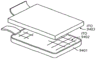
One embodiment of the present invention is concept C, which uses the laminate shown in fig. 13, thereby allowing a touch function separate from the LCD. In concept C, two additional Indium Tin Oxide (ITO) layers (ITO 11301 and ITO 21302) may be patterned on top of a Color Filter (CF) plate (e.g., a top glass layer). These layers may be used for touch sensing and touch driving components of a touch sensor, which may be a mutual capacitance touch sensor. These ITO layers can be patterned into columns and/or rows (shown in FIGS. 1 and 2 and described in the previous multi-touch sensing description) and can be separated by a dielectric, such as by a glass substrate or thin (e.g., 5-12 mm) SiO2The layers are separated.
In some embodiments, visual artifacts may be reduced by optimizing the electrode pattern used in the touch member. For example, FIG. 14 illustrates a diamond electrode pattern that can reduce visual artifacts.
In concept C, an FPC carrying touch sensing data may be attached to the top surface of the top glass 1303.
2.1.2 concept N
One embodiment of the present invention is concept N, which may implement capacitive sensing using self-capacitive sensing on the outer surface of a Color Filter (CF) panel. Concept N may use the stack-up shown in fig. 15, where the touch sensing elements may be located on top of CF plate 1501 (top glass). By forming the TFT 1503 having two metal layers and the patterned ITO 1500 on the CF plate 1501 using, for example, the same LTPS process as the conventional TFT plate 1504 process, a concept N-based LCD can be constructed without changing the standard LCD process. Touch ITO layer 1500 may be patterned into a plurality of touch pixels 1612 (fig. 16). The touch ITO layer 1500 may be protected with a plastic cover (as shown in fig. 17), and the plastic cover may also serve as a surface to be touched by a user.
FIG. 16 illustrates a self-capacitance touch pixel circuit for concept N. Each ITO touch pixel 1612 may be connected to two TFTs, such as an input TFT 1604 and an output TFT 1608. Input TFT 1604 may charge ITO touch pixel 1612 and output TFT 1608 may discharge ITO touch pixel 1612. The amount of charge moved may depend on the capacitance of ITO touch pixel 1612, which may vary by the proximity of a finger. More details regarding self-capacitance touch sensing are described above and in U.S. Pat. No. 6,323,846 entitled "Method and Apparatus for Integrating Manual Input," filed 11/27/2001, which is incorporated herein by reference in its entirety.
In one embodiment, as shown in fig. 16 and 18 for output column 1610 'C0' and output gate 1606 'R3', output column 1610 may be shared by touch pixels in the vertical direction and output gate 1606 may be shared by touch pixels in the horizontal direction. Fig. 19 shows a detailed layout of the touch pixels.
2.2 partially integrated touch sensing
Integrating touch sensing components inside the LCM can provide a number of advantages. For example, touch sensing components added inside the LCM may "reuse" an ITO layer or other structure that would otherwise be used only for display functions to provide touch sensing functionality. By incorporating touch sensing features into existing display layers, the total number of layers can also be reduced, reducing the display thickness and simplifying the manufacturing process.
The following embodiments may include touch sensing components inside and outside the LCM. Since integration of touch sensing components within the LCM can result in noise and interference between these two functions, the following designs can also include techniques that allow sharing of components while also reducing or eliminating the negative effects of electrical interference between the display and/or touch sensing on both outputs.
2.2.1 concept A
Concept a the base stack 2000 shown in fig. 20 can be used between the top glass and polarizer 2003, with an ITO sensing layer with multi-touch ("MT") capability (ITO1)2001 located on the user side of the top glass 2002. From the top, the touch sensing layer may include: ITO 12001 (an ITO layer that may be patterned into N sense (or drive) lines) and ITO 22004 (an ITO layer that may be patterned into M drive (or sense) lines). ITO 22004 can also act as V for LCDCOMAnd an electrode.
2.2.1.1 concept A: touch sensor electrode
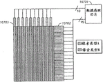
The touch sensor electrode array may include two patterned ITO layers as shown in fig. 21 (left side). FIG. 21 is a simplified view of one possible implementation of touch sensor electrodes. The layer ITO 12101 closer to the viewer may be a touch output layer, which may also be referred to as a sense layer or sense line. Touch drive layer 2102 may be located on layer ITO 2. ITO2 may also form capacitor CLC(see fig. 7). Further, fig. 21 (right side) also shows details of the three sensing pixels 2103a, 2103b and 2103c and their associated capacitors. The sensing lines and the driving lines have a pitch of 5mm and a gap of 10 to 30 μm. The gap may be small enough to be invisible to the naked eye but still large enough to be easily etched with a simple proximity mask (the gap is exaggerated in the figure).
Fig. 22 shows one possible physical implementation of concept a, including a top view 2201 and a side view 2202 with respect to cabling and subsystem placement. A top view 2201 shows the approximate position of the FPC 2203 in a deployed state (discussed in more detail below). FIG. 22 illustrates only one implementation in which a separate touch level shifter/decoder COG may be used. Alternative architectures that minimize the number of discrete touch elements will be discussed below. For mechanical stability, the FPC may be bent, as shown in side view 2202, to minimize the pressure applied at the T-tab (top joint) 2204 and B-tab (bottom joint) 2205 bond. FIG. 23 is a high level block diagram showing one possible architecture 2300 possessed by a primary bottom glass element, and a segmented ITO2 layer 2301 for touch sensing located on a top glass. For ITO2 on the top glass, each segment 2302 is connected to a corresponding pad on the bottom glass by a conductive dot 2303. Each pad on the bottom glass may be connected to a touch driver, as described below.
2.2.1.2 concept A: conductive point
Conductive dots at the corners of the LCD can be used to couple VCOMThe electrodes are connected to a drive circuit. Additional conductive points can be used to connect the touch drive lines to the touch drive circuitry. These points may have a sufficiently low resistance so as not to significantly increase the phase delay of the touch drive signal (discussed in more detail below). This may include limiting the conductive point resistance to 10 ohms or less. The conductive dot size may also be limited to reduce the required real estate.
As shown in fig. 24, elongated conductive dots 2401 may be used to reduce the requirements on dot resistance and real estate. The width of touch drive segment 2402 can be about 5mm, thereby providing a larger area to reduce the dot resistance.
2.2.1.3 concept A: flexible circuit and touch/LCD driver IC
A conventional display (e.g., fig. 9) may have an LCD driver Integrated Circuit (IC)901 for controlling the low-level operation of the display. The system host processor may exercise high level control over the display by sending commands and display data to the LCD driver 901. The multi-touch system may also have one or more driver ICs. An exemplary system with multi-touch capability is described in the incorporated reference, which includes three ICs, a multi-touch controller, an external level shifter/decoder, and a controller such as an ARM processor. The ARM processor may perform low-level control of the multi-touch controller and may then control the level shifter/decoder. The system host processor may perform advanced control over the ARM processor and receive touch data therefrom. In some embodiments, these drivers may be integrated into a single IC.
FIG. 25 shows an example high-level block diagram of a touch/LCD driver integrated circuit 2501. The IC has two main functions: 1) LCD control and update, and 2) touch scanning and data processing. These two functions can be integrated by an LCD driver portion 2502 for LCD control, an ARM processor 2503, and a multi-touch controller 2504 for touch scanning and processing. The touch circuitry may be synchronized with the LCD scan to avoid interference. Communication between the host and one of the LCD driver or ARM processor may be via host data and control bus 2505. A more fully integrated touch/LCD driver will be discussed below.
As shown in fig. 26, the FPC 2601 that brings together signals for the various touch and display layers may have three connector contacts, i.e., T-Tab 2602, B-Tab 2603, and host contact 2604. The T-tab may be connected to a sense line pad on the top glass. The T-tab trace 2605 may be connected to a corresponding pad on the B-tab 2603, and the B-tab 2603 may also be attached to the bottom glass. B-tab 2603 may also provide pass-through wiring 2606 from host connector 2604 to the touch/LCD driver IC, where host interface 2604 can connect a host to the touch/LCD driver IC. The FPC 2601 may also provide a substrate for each element 2607 supporting touch and LCD operations, and may be connected to the backlight FPC through two pads 2608.
The FPC 2601 may be a joint bonded to both the top and bottom glass. Alternatively, other bonding methods may be used.
2.2.1.4 concept A: touch drive integrated on bottom glass
The level shifter/decoder chip along with a separate voltage booster (e.g., 3V to 18V booster) may provide a high voltage drive circuit for touch sensing. In one embodiment, the touch/LCD driver IC may control the level shifter/decoder chip. Alternatively, the booster and/or the level shifter/decoder may be integrated in the touch/IC driver IC. For example, the integration may be achieved with a high voltage (18V) LTPS process. Doing so may allow for the level shifter/decoder chip and the voltage booster to be integrated on the bottom glass periphery. Level shifter/decoder may also be provided for V, as described belowCOMThe voltage of the touch drive is modulated.
2.2.1.5 concept A: and LCD VCOMShared touch drive
As described above, concept A can add an ITO layer to a standard LCD stackup, where the layer can function as a touch sensing line. The touch driving layer may be similar to LCD V, also denoted ITO2COMAnd (4) plane sharing. For display operations, a standard video refresh rate (e.g., 60fps) may be used. For touch sensing, a rate of at least 120 times per second may be used. However, the touch scan rate may also be reduced to a lower rate that matches the display refresh rate, such as 60 scans per second. In some embodiments, it is desirable not to interrupt display refresh or touch scan. Thus, one scheme that allows sharing of the ITO2 layer without slowing or interrupting display refresh or touch scanning (which may occur at the same or different rates) will now be described.
The concurrent display update and touch scan processing is depicted in FIG. 27. Five multi-touch drive segments 2700, 2701, 2702, 2703, 2704 are shown in this example. Each touch drive segment may overlap M display rows. The display may be scanned at a rate of 60 frames per second while the multi-touch sensor array may be scanned at a rate of 120 times per second. The figure shows the temporal evolution of a display frame lasting 16.67 milliseconds. The currently updated display area should preferably not overlap with the active touch drive segment.
Since the display scan is typically done in row order, the touch drive segments can be driven out of order to avoid overlapping display and touch activity. In the example shown in FIG. 27, the touch drive sequence is 1,2,3,4,0 in the first 8.3 milliseconds, and 1,2,4,3,0 in the second 8.3 millisecond cycle. The actual ordering may vary depending on the number of touch drive segments and the number of display rows. Thus, in general, it would be desirable if the touch drive usage sequence could be programmed. But for some special reasons a fixed sequence ordering may suffice.
Furthermore, it is also highly desirable (for image quality considerations) to have the active touch-driven segment away from the display area being updated. This is not illustrated in fig. 27, but is easily achieved when it is assumed that the number of touch driving segments is sufficient (e.g., 6 or more segments).
These techniques can effectively provide different refresh rates for the display and touch sensing components without requiring multiple circuits to support the high frequency display driver components.
2.2.1.6 concept A: vCSTDriving options
As shown in FIG. 7, VCSTAnd VCOMMay be connected together and thus can be commonly modulated to achieve a desired AC waveform across the LC. This is using VCOMModulation helps to achieve proper display refresh. In the process of mixing VCOMFor touch driving, it is not necessary to modulate V as wellCST. This process can be considered as the following open circuit VCSTAnd (6) selecting options. However, if V is usedSTMTo modulate VCSTThen the touch driving signal V can be reducedSTMThe capacitive load on the touch panel capacitively loads, thereby causing the phase delay of the touch signal to decrease. And this process can be regarded as driving V as described belowCSTAnd (6) selecting options.
FIG. 28 exampleShow an open circuit VCSTAnd (6) selecting options. The bottom diagram 2802 illustrates how one touch drive segment 2803 can cover M display rows 2804. Touch drive segment 2803 on the top glass can be electrically connected to circuitry on the bottom glass by conductive dots 2805. At the edge of display 2806, there are M V's in the M rows below the touch drive segmentCSTThe wires may be connected together. The top diagram 2801 shows the sub-pixel basic circuit, where the sub-pixel has a separate storage capacitor CST. In the top diagram, area 2807 may represent M consecutive rows of subpixels covered by a single touch drive segment. As described above, display operations and touch sensing may occur at different times for a particular touch drive/display set. When the display driver is ready to set the sub-pixel states in M rows, switches 2808, 2809 may turn V onCOMDrive2810 to M pieces of VCSTLine 2804 is connected to touch drive segment (V)COM)。VCOMThe Drive voltage may be set to ground or supply rail by the LCD driver depending on the inversion phase. Later, when this touch drive/display group is available for touch use, switches 2808, 2809 can connect the touch drive segment to V STM2811, and from VCOMDrive2810 disconnect VCSTThereby leaving it in the open state 2812.
FIG. 29 illustrates the driving VCSTAnd (6) selecting options. The bottom diagram 2902 illustrates how one touch drive segment 2903 can overlap with M display rows 2904. Touch drive segments 2903 located on the top glass can be electrically connected to circuitry on the bottom glass by conductive points 2905. At the edge of the display 2906, M V's in rows below a particular touch drive segmentCSTThe wires may be connected together. The top diagram 2901 shows a sub-pixel basic circuit, where the sub-pixel has a separate storage capacitor CST. In the top diagram, region 2907 may represent M consecutive rows of subpixels covered by a single touch drive segment. The display operation and the touch sensing may occur at different times. When the display driver is ready to set the sub-pixel states in the M rows, switch 2908 may set VCOMDrive2910 to M VCSTLine 2904 and to touch drive segment (V)COM). In general, VCOMThe voltage of Drive2910 may be set to ground or supply rail by the LCD driver depending on the inversion phase. Later, when this touch drive/display group can be used for touch use, switch 2908 can set V toCSTAnd touch drive segment (V)COM) To V STM 2911。
2.2.1.7 concept A: MT drive capacitive load
The capacitive loading of the touch drive lines of concept a can be very high, which can occur, for example, because there is a thin (e.g., about 4 μm) gap between the touch drive layer and the bottom glass, and the gap can be covered with a grid of metal wiring and pixel ITO. The liquid crystal may have a high maximum dielectric constant (e.g., about 10).
The capacitance of the touch drive segment may influence the stimulus touch pulse VSTMThe phase of (2) is delayed. If the capacitance is too high and thus there is too much phase delay, the resulting touch signal may be negatively affected. Applicants' analysis shows that if the ITO2 sheet resistance is kept at about 30 ohms/square or less, the phase retardation can be kept within optimum limits.
2.2.1.8 concept A: electric model and VCOMIntroduced noise
Since ITO2 can be used for touch driving and LCD V simultaneouslyCOMTherefore, if it is for VCOMThe modulation adds noise to the touch signal.
For example, while using one touch drive segment for touch sensing, if V is usedCOMTo modulate another touch drive segment, it is possible to add a noise component to the touch signal. The amount of noise added depends on the amount of noise relative to VSTMV ofCOMPhase, amplitude and frequency of the modulation. VCOMDepending on the inversion method used for the LCD.
FIG. 30 shows an electrical model of the use of touch driver 3001 for touch sensing and LCD VCOMThe modulation condition.The model shows VCOMThe input path through which noise can be added to the input terminal of the charge amplifier 3002 is modulated.
In some embodiments, the charge amplifier 3002 may require additional headroom (headroom) to accommodate V COM3003 introduced noise. In addition, subsequent filtering circuitry (e.g., a synchronous demodulator, not shown) may need to remove the signal from VCOMThe resulting noise signal is modulated.
2.2.1.9 concept A: vSTMEffect
Under certain conditions, VSTMModulation may have a negative impact on the subpixel voltage under the touch drive segment being modulated. If a perceptible change in subpixel RMS voltage occurs, display artifacts may result. To minimize display distortion that may result, one or more of the following methods may be utilized.
Touch driving from both sides can reduce distortion of LC pixel voltages. As shown in fig. 31, by adding VSTMTo C on both sides via conductive points 3102STWire, can be made by using the existing low resistance C on the bottom glassSTThe wiring 3101 realizes touch driving from both sides. Alternatively, single-ended touch driving may produce a pixel offset voltage that is uniform for all pixels, and this voltage may be reduced or eliminated by adjusting the data drive level. In addition, reducing ITO sheet resistance also helps to reduce display artifacts. Finally, VSTMCan also be associated with VCOMIs correlated with frequency to reduce the amount of noise in the touch signal.
2.2.1.10 concept A: influence on the manufacturing process
The fabrication process of concept a may include additional steps associated with a typical LCD fabrication process. Some of these steps may be entirely new steps and some steps may be modifications to existing steps. Fig. 32 shows a manufacturing process flow of concept a. Blocks 3201, 3202, and 3204 represent new steps, and blocks 3205, 3206, and 3207 represent modified steps, both of which are related to a conventional LCD manufacturing process (e.g., the manufacturing process of fig. 8).
The coating and patterning of ITO1 (blocks 3201, 3202) may be accomplished using known methods. The ITO may be protected during the rest of the LCD processing. Photoresists may be used to provide a removable protective coating. Alternatively, silicon dioxide may provide a permanent protective coating. In addition, ITO2 can be coated and patterned (block 3204) to form touch drive segments in a similar manner.
Phase delay analysis shows that for small displays (≦ 4 "diagonal), the sheet resistance of ITO1 and ITO2 may be as high as 300 ohms/square assuming less capacitive loading on either plane. As described above, it may be desirable for the capacitive load incorporating concept a to have a magnitude that limits the maximum sheet resistance of ITO2 to about 30 ohms/square or less.
2.2.2 concept A60
Concept a60 is physically similar to concept a and may provide a different approach to the problem of synchronizing display updates and touch scans. The treatment may be carried out by subjecting V toCOM1-line inversion of (i.e., V) is used as a stimulus for the touch signalSTM) To complete. This is illustrated in FIG. 33, which shows how a single touch drive segment 3301 can be modulated while the other touch drive segments can be held at a constant voltage. The method can eliminate the removal of unwanted V from the touch signalCOMThe problem of noise introduced. Furthermore, the display update and touch sensor scan are not necessarily spatially separated. But using this method, it is possible to operate at a single frequency (i.e., V)COMModulation frequency, e.g., about 14.4kHz), as opposed to the multi-frequency demodulation described in U.S. patent application 11/381,313 entitled "Multipoint Touch Screen Controller," filed on 2.5.2006, which is incorporated herein by reference. In addition, using this approach, the touch sensor scan rate can be fixed at the video refresh rate (e.g., 60 times per second).
2.2.3 concept B
Concept B illustrated in fig. 34 is similar to concept a, both sharing many of the same electrical, cabling and structural characteristics. However, concept B mayIntegrating touch drive layers into VCOMIn a layer. Concept B therefore differs in the number and stacking position of ITO layers used for LCD and touch sensing. Because of these similarities, concept B will now be described by emphasizing the differences between concepts a and B.
Concept B may split the shared ITO2 layer in concept A into two ITO layers, one layer serving as touch sensing (ITO)3402 and the other layer serving as LCD VCOM(ITO3) 3403. From the top, the layers for touch sensing may include: ITO 13401, which is an ITO layer that can be patterned into N touch sense lines; ITO 23402, which is an ITO layer that can be patterned into M touch drive lines; and ITO 33403, which is a V that can function as an LCDCOMAn ITO layer of the electrode. A touch driving layer (ITO2)3402 may be deposited on the lower surface of the top glass 3404, above the color filters 3405.
By separating V from touch-driven partCOMInterference can be reduced.
2.2.3.1 concept B: touch sensor electrode
Concept B may include touch sensor electrodes substantially similar to the electrodes described above for concept a.
2.2.3.2 concept B: conductive point
As with concept A, concept B can use additional conductive points 3406 located at the corners of the LCD to connect the touch drive segments to dedicated circuitry. Since V does not have to be shared with touch sensingCOMThus concept B can retain those VCOMConnected to each corner point of its driving circuit. In addition (as described below), concept B may even be VCOMMore conductive dots are added.
2.2.3.3 concept B: flexible circuit and touch/LCD driver IC
Concept B may use substantially the same FPC and touch/LCD driver IC as described for concept a.
2.2.3.4 concept B: synchronizing with LCD scanning
For concept B, although VCOMLayers may be separate from the touch drive layer, but it is still desirable to synchronize touch scanning and LCD updating in order to physically bring about a livenessThe moving touch drive is separate from the display area being updated. For concept B, the synchronization scheme previously described for concept a is equally applicable.
2.2.3.5 concept B: MT drive capacitive load
Like concept a, the capacitive load on the touch drive line of concept B can be very high. The large capacitance may be driven by touch drive (ITO)3402 and VCOMThin (e.g., about 5 μm) dielectric between planes (ITO3) 3403. One approach for reducing undesirable phase delay in touch stimulation signals is to reduce ITO drive line resistance by adding parallel metal traces. Phase delay may also be reduced by lowering the output resistance of the level shifter/decoder.
2.2.3.6 concept B: electric model and VCOMIntroducing noise
Due to the whole VCOMThe planes may all be coupled to the touch drive layer, so that operation of the multi-touch charge amplifier is likely to be VCOMThe noise disruption introduced by the modulation. To mitigate these effects, concept B may have a constant VCOMA voltage.
In contrast, ITO 23402 and ITO 33403 (V)COMAnd touch driving) may interfere with VCOMVoltages, which may result in storing erroneous data voltages on the LC pixels. To reduce VSTMTo VCOMCan increase the voltage VCOMThe number of conductive points connected to the bottom glass. For example, except for V at each corner of the viewing areaCOMIn addition to dots, conductive dots may also be placed in the middle of each edge.
By mixing VSTMAnd VCOMSynchronization, and turning off the pixel TFT at the correct time, can be further reduced by VCOM-VSTMDistortion caused by coupling. For example, if the line frequency is 28.8kHz and the touch drive frequency is a multiple of that frequency (e.g., 172.8kHz, 230.4kHz, and 288kHz), then VCOMThe distortion may have the same phase relationship for all pixels, thereby reducing or eliminating VCOMVisibility of the distortion. Furthermore, when the distortion is mostly attenuatedIf the gate of the pixel TFT is turned off, the LC pixel voltage error can be reduced. Like concept A, VSTMMay be in phase with V and frequencyCOMIs correlated with frequency to reduce the amount of noise in the touch signal.
2.2.3.7 concept B: influence on the manufacturing process
Like concept a, concept B may also add a step in the LCD manufacturing process. Fig. 35 shows a manufacturing process flow for concept B, where blocks 3501, 3502, 3503 and 3504 represent new steps associated with a conventional LCD manufacturing process (e.g., the process described in fig. 8), while blocks 3506, 3507, 3508 and 3509 represent modifications made to existing steps (e.g., the steps also associated with fig. 8).
As with concept a, ITO1 may be coated (block 3501) and patterned (block 3502) using known methods. The sheet resistance of ITO1 and ITO2 is substantially similar to that described for concept a. For concept B, since the layer of ITO2 may be coated directly on the glass, its deposition (block 3503) may be a routine process. Electrical access between the ITO2 layer and the bottom glass can be easily accomplished for those conductive points connected to the touch drive segments by etching using a shadow mask.
ITO3 (e.g. V for LCD)COMLayer) may have a sheet resistance between 30 and 100 ohms per square, and it may likewise be applied using conventional methods (block 3505). However, as mentioned above, VCOMVoltage distortion can be reduced by reducing the ITO layer resistance. The effective resistance of ITO3 can be reduced, if necessary, by adding metal traces parallel to the touch drive segments. The metal traces may be aligned with the black matrix so as not to interfere with pixel opening (pixel addressing). In addition, the density of metal traces (between one per display row to about one per 32 display rows) can be adjusted to provide VCOMThe desired resistance of the layer.
2.2.4 concept B'
Concept B' may be understood as a variation of concept B, except that it omits the ITO2 driver layer and instead uses a conductive black matrix (e.g., CrO under the top glass)2Layer) as a touch driving layer. Alternatively, the metal driving lines may be hidden behind a black matrix, which may be a polymer black matrix (polymer black matrix). Doing so may provide several benefits, including: (1) an ITO layer is omitted; (2) reduce VSTMTo VCOMThe influence of the layer; and (3) simplifying the manufacturing process. Since the use of a black matrix for touch driving may eliminate the need for patterning an ITO layer over the color filter, the manufacturing process may be simplified.
Fig. 36 shows a side view 3601 and a top view 3602 of concept B'. It can be seen that side view 3601 looks much like a standard LCD stackup, except for top ITO layer 3603 for touch sensing. The lower graph of FIG. 36 shows how the black matrix 3604 can be divided into separate touch drive segments. The grid pattern may follow the pattern of a conventional black matrix, but each drive segment may be electrically isolated from the other segments. To compensate for the reduced touch signal strength that may result from using a black matrix as the touch drive, the charge amplifier gain may be increased (e.g., about 4X).
Since the touch sensing layer is not necessarily in contact with VCOMLayer shield, thus VCOMThe modulation may interfere with the touch signal. In addition, touch driving still has the possibility of interfering with VCOMA voltage. These two problems are addressed by the pair V described above in connection with concept ACOMSegmentation of the layers and/or spatial separation of display updates and touch sensing as described above can be addressed. Furthermore, a constant V can be usedCOMVoltage to address these issues.
2.2.5 concept K
Concept K is illustrated in fig. 37 (circuit diagram) and 38 (stack diagram). Concept K exploits the fact that C is used on the gateST(CSTOn-gate) configuration, a select pulse in the TFT LCD may be partially transmitted to the pixel ITO.
As shown in the display stack of fig. 38, a viewer may face the active array board 3801 instead of the CF board 3802. ITO pixels on active array 3803 can provide V for touch sensorSTMPulses in which display lines are alternated for VSTMPulsing and display addressing. The ITO sensing layer 3804 on the plastic polarizer 3805 may be laminated on the back side of the array plate 3801 to provide a touch sensing layer. Furthermore, a thin glass layer (e.g. 0.2mm) also contributes to an improved signal-to-noise ratio.
During a display update, each row may be individually selected to update pixel data (as shown in FIG. 39). To generate V for touch sensingSTMMultiple rows 4001 can be selected simultaneously, while a high data voltage 4003 is applied to the column line 4002 to keep the TFTs off (as shown in fig. 40). The column driver may adjust the timing of the data signals from the display memory to correspond to the touch drive time interval.
In one embodiment, the touch pulse sequence may pulse about 30 rows 4001 simultaneously during one touch scan interval. FIG. 41 shows touch drive pulses (V)STM) The effect on the LCD sub-pixel voltage. From VSTMThe voltage added by the pulse can be VCOMAnd/or gamma correction of gray values of the display data.
Concept K may provide a number of advantages. Since the display pixels and touch sensors share drive circuitry, the level shifter/decoder can be omitted. In addition, conventional CF plates may be used herein. In addition, no additional conductive points are required between the top and bottom glasses. The baseline (busline) reflection may increase the reflectivity (R) of certain portions of the display, thereby requiring the use of additional films (e.g., CrO under Cr) at the baseline that may reduce R.
2.2.6 concept of X'
The concept X' is illustrated in fig. 42 (circuit diagram) and fig. 43 (stack diagram). The concept X' exploits the fact that VSTMPossibly similar to the gate pulse (e.g., 15-18V swing) used for TFT pixel switching. In concept X', touch drive segment 4301 may be part of an LTPS active array and may form a pixel storage capacitor CSTCounter electrode (counter electrode). CSTMay be formed between two ITO layers 4301, 4302. In this embodiment, the active array plate 4303, rather than the color filter plate 4304, may be located on the user side of the display.
As shown in FIG. 42, with a V forSTMMay be shared by three rows of pixels 4202 in order to select these rows. ITO touch drive segment 4203 may be patterned under a set of rows adjacent to the row being addressed. At a position different from VSTMWhen connected, these touch-driven segments 4203 can be connected to GND (ground) through TFT 4204.
Changes made to the processing steps to construct concept X' may include the following. First, a patterned sensing ITO can be added on the outside of the array substrate. Second, SiO can be added on the sensing ITO during LTPS processing2And (4) protecting. In addition, a protective resist (resist) may also be used here. Third, touch-driven ITO can be used in SiO for LTPS arrays2A barrier layer (which may be found in a typical LTPS process) is deposited and patterned underneath. Finally, the vias may be in the barrier SiO2Is patterned so as to be in contact with the touch driving ITO layer. This step may be combined with subsequent processing steps.
The concept X' may also provide a number of advantages. For example, since the display and touch sensor share the drive circuitry, the level shifter/decoder chip may be omitted. Further, no change is required to the CF plate, whereby a conventional color filtering process can be used. Further, due to the storage capacitor CSTCan be located between two ITO layers and thus can achieve very high transmission. In addition, another advantage is that additional conductive points between the array plate 4303 and the CF plate 4304 may be omitted.
2.3 fully integrated touch sensing
A third set of embodiments of the present invention fully integrates the touch sensing components inside the LCM. As with partially integrated touch sensing, existing layers in the LCM can simultaneously serve dual tasks in order to provide touch sensing functionality, and thereby reduce display thickness and simplify manufacturing processes. In addition, these fully integrated touch sensing layers may also be protected between glass layers.
In some embodiments, a fully integrated LCD may includeV similar to that described in the previous embodimentCOMAnd (3) a layer. In other embodiments, a fully integrated touch-sensing LCD may include in-plane switching (IPS) LCD structures, which will be described in more detail in subsequent sections.
2.3.1 fully integrated V-basedCOMLCD of (1)
2.3.1.1 concept A'
Concept a' can be considered a variation of concept a that omits the ITO sensing layer (ITO 2001 in fig. 20) and employs a conductive black matrix layer (located below the top glass) as the touch sensing layer. Alternatively, the metal sensing line may be hidden behind a black matrix, wherein the black matrix may be a polymer black matrix. Thus, concept A' may also eliminate the T-tab on the FPC and the corresponding adhesion to the top glass. The touch sensing lines may be routed to the bottom glass through conductive dots and may be directly connected to the touch/LCD driver chip. Further, the FPC may be a standard LCD FPC. By omitting manufacturing steps and elements, costs can be reduced compared to concepts a and B.
FIG. 44 illustrates one method that can be implemented to replace the touch sensing layer with a conductive black matrix. Fig. 44 includes a side view 4401 of the upper portion of a single pixel having a black matrix 4403 extending between three primary color portions 4404. The touch drive segments 4405 can be separated from the black matrix lines 4403 by a planarized (planarizing) dielectric layer 4406. Fig. 44 also shows a top view 4402 of a display having vertically extending black matrix lines 4403. About 96 black bottom lines (which is equivalent to 32 pixels, for example) may be connected together to the negative terminal of the charge amplifier 4907. The touch drive segment 4405 can be driven in the manner described above. A finger approaching the top glass 4408 may disturb the electric field between the vertical black matrix lines 4403 and the touch drive segments 4405. This perturbation may be amplified by the charge amplifier 4407 and may be further processed as described elsewhere herein.
Due to the depth of the touch sensor lines 4403 in the display, the minimum distance between a finger or touch object and the sensor lines 4403 may be limited. This reduces the touch signal strength. This can be addressed by reducing the thickness of the layers above the touch sensing layer, thereby allowing a finger or other touch object to be closer to the sense line.
2.3.1.2 concept X
Concept X is illustrated in fig. 45 and 46. The stack of concept X shown in fig. 45 is substantially equivalent to that of a standard LCD. Touch sensing layer 4501 can be embedded with VCOMLayer (ITO2) which serves the dual purpose of providing VCOMVoltage plane and as output of the touch sensor. The touch driving layer may also be embedded in an existing LCD layer. For example, touch drives can be located on the bottom glass 4503 and can be part of the LCD select line circuitry (see FIG. 5). The select line may then serve the dual purpose of providing the gate signal for the sub-pixel TFT and providing the touch drive signal VSTM. FIG. 46 is a top view of concept X, showing its floating pixel 4601 embedded VCOMOne possible arrangement of touch sensing layers of a layer.
2.3.1.3 concept H
Concept H is depicted in FIGS. 47-50. Concept H does not require any ITO to be included outside the top glass or plastic layer of the display. Thus, the manufacturing process may be very similar to existing display manufacturing processes.
As shown in fig. 47, the touch sensing portion of the screen may be a transparent resistive sheet (resistive sheet)4701, such as a glass or plastic substrate on which an unpatterned ITO layer is deposited. V of displayCOMA layer may be used for the touch sensing portion. In contrast to some embodiments described above, since the layer does not need to be patterned, a photolithography step may be omitted in the manufacturing process. For ease of reference herein, the sides are referred to as north, south, east and west as shown.
A plurality of switches 4702 may be disposed around the periphery of the resistive sheet. These switches may be implemented as TFTs on glass. In addition, in the display border area, a plurality of conductive dots 4703 are also displayed at each switch position, which can couple VCOM(on the top glass) to the TFT layer on the bottom glass. The switch 4702 may be commonly connected to two buses, e.g., north and east switches connected to one bus 4704And the south and west switches are connected to a second bus 4705.
For touch sensing, the switch 4702 may operate as follows. North and south switches may be used to measure the capacitance in the Y direction. The left and right switches can then be used to measure the capacitance in the X direction. Switches located in the northeast and northwest corners may be used for both X and Y measurements. As shown in fig. 49, the modulation can be performed by using a modulation waveform VMODThe resistive patches 4701 are actuated to measure capacitance. Further, the current (i.e., charge) required to drive the sheet to a desired voltage may be measured and used to determine the location of the touch.
In particular, as shown in the waveform of FIG. 49, in the absence of a touch, the baseline capacitance 4902 may indicate the stimulation of the lamella 4701 to VMODThe current (charge) required for the voltage. If there is a touch, a larger current 4903 (charge) may be required due to finger capacitance. This larger current is illustrated in the lower waveform group. The touch location can then be determined by a simple mathematical combination of the baseline and signal waveforms shown in fig. 49.
An equivalent circuit for a touch screen in performing an X-direction (i.e., east-west) measurement is illustrated in fig. 48. C _ PARA 4801 can be a distributed parasitic resistance of the sheet, and C _ filler 4802 can be a touch capacitance, e.g., a touch located at about 75% of the way to the east. The block diagram indicates how the plate can be driven to VMODAnd how the charge can be measured, combined, and processed and sent to the host.
Fig. 50 illustrates how concept H can be integrated with an LCD. In particular, conductive dots 5001 can be connected to the TFT layer to allow for a resistive sheet 5002 (V)COM) Modulation is performed to perform a display operation. The touch sensing operation and the display operation may be multiplexed in time. For example, assuming a screen refresh rate of 60Hz corresponding to a LCD update period of 16ms, a portion of this time may be used for writing information to the LCD, while another portion of the time may be used for touch sensing. During LCD refresh, VMODMay be from the LCD driverV of roadCOM. In touch sensing, waveforms with different frequencies and amplitudes may be used depending on the exact details of the touch system, such as desired SNR, parasitic capacitance, and so forth. It should be further noted that the touch sensing circuit in the present embodiment illustrated in block diagram form may be integrated in the LCD driver or may be a separate circuit.
2.3.1.4 concept J
Like concept H, concept J also does not require any ITO to be included outside the top glass or plastic layer of the display. The physical structure of concept J is illustrated in fig. 51. The touch sensing surface may be a resistive sheet 5101 similar to concept H, but patterned into a plurality of row strips 5102. The patterning process may be accomplished by photolithography, laser deletion (laser deletion), or other known patterning techniques. By patterning the resistive sheet 5101 into a plurality of strips 5102, the switches along the top and bottom (north and south) can be omitted, leaving the east and west switches 5103 connected to the row strips. Each row 5102 may be sequentially energized, for example using V as shown in FIG. 52MOD Waveform 5201. The current (charge) required to drive each row 5102 to a modulated voltage can be a function of the row capacitance, which can be a combination of the parasitic capacitance of the designated row (C _ PARA 5301, figure 53) and the capacitance of a FINGER or other touch object (C _ filler 5302, figure 53).
As shown in FIG. 52, the signal in the presence of a touch 5202 can be mathematically combined with the baseline signal 5203 to calculate touch coordinates. The Y output may be determined by the centroid of the Z output for each row. The X output may then be determined by a weighted average of the X outputs of each row.
Fig. 54 shows how the touch sensor of concept J can be integrated with an LCD. Conductive dots 5401 can connect V on top glassCOMA TFT layer connected to the bottom glass. Touch and display operations are not necessarily time multiplexed. Instead, while one portion of the display is being updated, another portion may be scanned for touch activity. Various techniques for accomplishing this are discussed above in connection with other embodiments. The touch sensing may use different frequencies and amplitudes,but may also be phase synchronized with the LCD line inversion. The switch 5402 may be implemented as a TFT on glass. The measurement circuit may be either integrated with the LCD controller or a separate component.
2.3.1.5 concept L
In concept L, an active TFT layer may be added to the color filter glass to allow the segmented ITO layer to provide multiple functions simultaneously via different regions of the LCD display. A stacked view of concept L is illustrated in fig. 55. Concept L may contain the same number of ITO layers as a standard LCD display. However, while the ITO 15509 and other structures 5507, 5508 on the bottom glass 5511 can remain standard, the active TFT layer 5501 on the filter glass 5505 can allow for regions (e.g., horizontal rows) of ITO 25504 at VCOMTouch driving or touch sensing.
Fig. 56 illustrates a conceptual L display with a horizontally segmented ITO2 layer 5504. The following processes are performed simultaneously for different areas of the display: execution VCOMModulation (region 5601) and/or writing (region 5602); providing touch stimulus (region 5603); providing touch sensing by measurement (region 5604); and maintained in a holding state (region 5605). The transistors in the active TFT layer 5501 may switch the signal for each horizontal row to the desired function in a specified time interval. In the same sequence, each region may have an equal exposure for each state, thereby substantially eliminating non-uniformities. Since providing touch stimulus can disturb the voltage across the LC, the LCD pixel writing process can occur immediately after the touch stimulus phase to shorten the duration of any disturbance. The LCD pixel writing to a region can be at VCOMOccurs during modulation, while adjacent segments may experience VCOMModulated to maintain uniform boundary conditions during pixel writing.
The color filter plate may be formed using a process similar to that used for active array processing. The process of forming the additional TFT layer may involve additional steps, but the back-end processing of the two substrates may remain substantially similar to that of a standard LCD. These techniques may allow such displays to be suitable for larger size panels without the use of low resistance ITO.
2.3.1.6 concepts M1 and M2
Fig. 57 and 58 show a stack of diagrams of the concepts M1 and M2, respectively. Concepts M1 and M2 may add patterned ITO and metal layers to the filter glass for touch sensing. Although the concepts M1 and M2 are similar, one difference is the different uses of the ITO1 and ITO2 layers. Concept M1 may use ITO 15701 for touch sensing and ITO 25702 for VCOMBoth (when the LCD pixel voltage is set/held) and touch driving (when the pixel voltage is not written). Concept M2 may use ITO 15801 for touch drive and ITO 25802 for VCOMAnd touch sensing. For both concepts M1 and M2, the top glass 5703, 5803 need not include any transistors or other active elements.
In either concept M1 or M2, V may be pairedCOMSegmentation to allow a display area to maintain a constant V during display updateCOMWhile another area is independently scanned for touch activity. This may reduce interference between touch sensing and display functions.
Fig. 59, 60, and 61 show an exemplary display (corresponding to concept M2) segmented into three regions (5901, 5902, 5903; fig. 59) where two regions may perform touch scans simultaneously (e.g., regions 5901, 5902) and the display pixels of the third region may be updated (e.g., region 5903). On the left side of FIG. 61, 27 vertical drive lines 6101 at the ITO1 and M1 (Metal 1) layers can provide three different areas, each of which has 9 touch columns. Each drive line (3 per touch column) may have a conductive point down to the array glass and may be routed to a driver ASIC (not shown).
The right side of FIG. 61 shows a possible pattern of segmented horizontal rows for the ITO2 layer, including V for the first set of alternating rows 6102COMAnd VHOLDAnd V for a second set of alternating rows 6103COM、VHOLDAnd VSENSE. Each row of ITO2 may be connected down to the array via conductive dots (not shown)Column glass, whereby LTPS TFT switches can be used to switch row mode. The right side of fig. 61 shows 21 sense rows, of which 14 can be sensed at any time (but the other number of rows can be more).
FIG. 62 shows a circuit diagram for touch sensing for the exemplary displays shown in FIGS. 59, 60, and 61. VSTMThe driver 6200 sends a signal through a metal drive column 6202, which may have a resistance RMetcolAnd parasitic capacitance Cdrv. Touch capacitance CsigCan be measured via an ITO line, which can have a resistance Rito2rowAnd a parasitic capacitance Cito2row. It is also possible for the touch sense charge to be subjected to two additional resistors R before reaching the charge amplifier 6204sw1And RborderThe influence of (c).
A display frame update rate of 60fps may correspond to a touch scan rate of 120 fps. If desired (e.g., in a small multi-touch display), the designer may choose to reduce the touch scan rate (e.g., to 60fps), thereby saving power and potentially reducing complexity. Thus, certain areas of the display may be left in a "hold state" when neither display updates nor touch scans occur in those areas.
Fig. 63 shows a display (as in fig. 60) in which the display area can be scanned and updated horizontally instead of vertically. The touch drive and touch sense areas can be interleaved so that stimulation applied to a touch drive row 6301 can be sensed from both sense rows 6302 and 6303 simultaneously, as shown by sense field lines 6305.
A black mask layer may be used to hide metal lines and/or gaps in the ITO layer. For example, the metal drive lines in ITO2, the etched gaps, and the etched gaps in ITO1 may be completely or partially hidden behind a black mask (as shown in fig. 64). This may reduce or eliminate the visual impact of these items on the display user.
2.3.1.7 concept M3
As shown in fig. 65, the concept M3 may be similar to the concepts M1 and M2, but it integrates touch driving and touch sensing in a single segmented ITO layer 6501. Although the various embodiments described above include the drive and sense electrodes on separate layers, the concept M3 may include the drive and sense electrodes in the same plane. By adding the dielectric layer 6502, the touch sensing component can be shielded from other electric fields and/or effects.
Fig. 66 and 67 illustrate the display of the concept M3 segmented into three regions 6601, 6602, 6603, each of which may alternate between a touch excitation/sensing phase, an LCD pixel writing phase, and a hold phase during each cyclic update of the display frame. FIG. 68 illustrates wiring details and layout settings that can divide the display. ITO1 row 6801 may be connected to LTPS switches on the TFT glass via conductive dots 6802, where the switches would be at V for that rowCOMAnd VHOLDTo switch the voltage. Three sense lines 6803 (one for each region) can be used for each column, where the lines are to be multiplexed to measure the active region in the corresponding time frame. In performing touch scanning on a certain area, a touch driving part corresponding to a row in the area may be activated, and all columns of the row may be sensed at the same time. During the time that one area of the display is scanned for touch activity, another area may modulate VCOMAnd/or update display pixels.
By adding metal segments (6805 in fig. 68) to the regions of ITO, the resistance of the ITO can be reduced. For example, short metal segments may be added to ITO1 drive electrodes 6804 to reduce the phase delay of the touch signal. These metal lines may be hidden behind a black mask layer.
As shown in fig. 69, guard traces 6903 can be used to block field lines between the touch and sense electrodes that are not passed up by the glass, in which case they would be affected by a finger or other touching object. This may reduce noise and enhance the impact of the measured touch on the display. FIG. 70 shows a top view 7001 and a cross-sectional view 7002 of a display without guard traces where rows of touch sensing components, such as drive electrodes 7003 and sense electrodes 7004, are separated by narrow gaps. When touch sensing is activeBy depositing a layer 6905 (V) of ITO2COM) Grounded, the touch sensing and display functions may be shielded from each other. FIG. 69 shows a top view 11101 and a cross-sectional view 6902 of a display including touch sensing components, such as ground guard traces 6903 between rows of drive electrodes 6904 and sense electrodes 6905, disposed on ITO 1.
2.3.1.8 concepts P1 and P2
Concepts P1 and P2 are similar to concept M3 and can provide touch driving and touch sensing electrodes in the same plane. However, as shown in FIG. 71, the concepts P1 and P2 may also provide the additional benefit of being individually addressable touch pixels. Each touch pixel can include a drive electrode 7102, a sense electrode 7103, and corresponding drive 7104 and sense lines 7105 that can be routed separately and connected to a bus on the display border. These lines may be formed using a conductive black mask, thereby allowing the black mask areas already present in the display to provide additional services for touch sensing. Alternatively, these lines may also be metal lines arranged behind a black matrix, wherein the black matrix may be a polymer black matrix.
Fig. 72 shows a stack diagram of concept P1. The concept P1 may differ from standard LCD processing in various ways. For example, a portion of the standard polymer black matrix may be changed to black chrome with a low resistance metal backing. These conductive lines can then be used to route signals to and from the touch pixels. In an additional masking step, a patterned ITO layer 7202 may be added behind the black mask. By adding STN type conductive dots 7203, drive and sense signals for each touch pixel can be routed to the LTPS TFT board (e.g., 2 dots per touch pixel). In addition, color filter layers and boundary planarization layers 7204 can be thickened to reduce touch driving and VCOMThe capacitance between them.
Fig. 73 shows a stack diagram of concept P2. In addition to incorporating the four variations described above with reference to concept P1, concept P2 may also include a patterned ITO layer 7301, where the layer may be used to create segmented VCOM. By pairs of VCOMSegmented, touch-driven and display operations can be isolated byThis potentially improves the signal-to-noise ratio. FIG. 74 shows a V highlighting concept P2COMCircuit diagram of signal coupling. By maintaining separate buses (Vholdbus1 and Vholdbus2) for return, the coupled charge can be reduced. Furthermore, by using complementary drives for half of the touch pixels, the backflow in Vholdbus1 may be reduced.
FIGS. 71 and 75 illustrate exemplary routing of touch sense and touch drive lines to and from the sense and drive pixels. A set of drive and sense lines can be routed horizontally from bus lines 7501, 7502 at each end of the display to each individual touch pixel 7101. These lines may be hidden behind a black mask layer or may also be incorporated into a conductive black mask layer. Furthermore, such wiring may also be located on a single layer. Signals for individual touch pixels can be addressed and multiplexed using LTPS TFTs and over bus lines.
Parasitic capacitance can be reduced if individual pixels can be driven instead of the entire row. In addition, the individually addressable touch pixels also allow the touch array to be scanned in a "random access" mode, not just in a row-by-row mode. This may increase the flexibility of the process of interleaving touch sensing with display updates. For example, fig. 76 depicts one possible scan pattern. Since the system can scan the touch pixels in any desired pattern, the scan pattern can be designed to ensure that adjacent rows and adjacent pixels are never driven at the same time, thereby avoiding fringe field (fringe field) interactions that can lead to signal loss or signal-to-noise ratio reduction. In FIG. 76, blocks 7601 and 7602 each include a drive electrode and a sense electrode. Block 7601 corresponds to an in-phase drive, while block 7602 corresponds to a 180 degree out-of-phase drive signal. In this figure, two rows (24 pixels total) may be overlaid in five sequences and four pixels scanned at a time.
2.3.1.9 concept D
Another embodiment, concept D, may support a multi-touch sensing process by using two segmented ITO layers and additional transistors for each touch pixel. Fig. 77 shows a circuit diagram of concept D. Updating on displayIn the process, the circuit may function as in a standard LCD display. Gate drive 7700 can drive two transistors (Q17702 and Q27704), thereby allowing for power from VCOMSignals on bus 7706 and data line 7708 convey charge to a set of circuits for controlling the LC (C)ST7710、CLC17712 and CLC27714) The capacitor of (2). When transistor Q27704 is turned off, V COM7706 it will be disconnected from C ST7710, thereby allowing V to be insertedCOM Line 7706 is used for touch sensing. In particular, line 7706 can be used to pass charge through C IN7716 and C OUT7718, via data lines 7708 (used as touch sense lines) into charge amplifier 7720. Conductive objects (e.g., a user's finger, a stylus, etc.) in proximity to the display can perturb the system capacitance in a manner that can be measured by charge amplifier 7720.
Fig. 78 and 79 show sub-pixel overlay diagrams in a concept D based display. In fig. 78, the layer of ITO1 may be segmented into two plates, a 7722 and C7726. The layer of ITO2 may be segmented into islands (e.g., B7724) that may be located over the subpixels and act as counter electrodes for the plates in the layer of ITO 1. During a display update, the voltage difference between the islands 7724 and the plates (a 7722, C7726) may be used to control the liquid crystal 7804. During touch sensing, the perturbation in capacitance throughout the subpixels (e.g., CLC1, CLC2, Cin, Cout, and Cst in fig. 77) may be measured therein to determine the proximity of conductive objects.
Fig. 80 shows a combined wiring stack diagram of concept D. FIG. 81 illustrates a physical implementation of one embodiment of concept D.
2.3.2 fully integrated and IPS-based LCD
In fig. 82, in-plane switching (IPS) is schematically illustrated, which can be used to create an LCD display with a wider viewing angle. While some LCDs (e.g., twisted nematic) use vertically arranged electrode pairs (a related example is shown in fig. 20), in an IPS LCD, the two electrodes 8201, 8202 for controlling the orientation of the liquid crystals 8203 can be parallel to each other in the same layer (e.g., in a single plane). By orienting the electrodes in this manner, a horizontal electric field 8200 can be generated across the liquid crystal, which can cause the liquid crystal to be parallel to the front of the panel, thereby increasing the viewing angle. The liquid crystal molecules in an IPS display are not anchored to the upper or lower layer (relevant examples are shown in fig. 82), but instead can rotate freely to align themselves to the electric field 8200 while remaining parallel to each other and to the plane of the display electrodes. FIG. 83 shows a more realistic setting of interdigitated pairs of electrodes (electrodes) 8301, 8302 in a display where planar switching may be used.
Due to the IPS display lacking V available for touch actuation or touch sensingCOMThus, certain embodiments of the present invention may allow the same electrodes used for display updating to be used for touch sensing as well, in order to provide touch sensing capabilities. These electrodes may be supplemented by additional circuitry (compensated). In some embodiments described above, it is possible for a touch pixel to overlap a large number of display pixels. In contrast, since the below-described IPS embodiments can use the same electrodes for display control and touch sensing, higher touch resolution can be achieved with little or no additional cost. Alternatively, multiple touch pixels can be aggregated to produce a combined touch signal of lower resolution.
2.3.2.1 concept E
One IPS embodiment, concept E, is illustrated in FIG. 84. As described above, in the IPS-based touch sensing display, the electrodes may be in the same plane and may have an interdigital structure (as shown in fig. 84). Although electrode a 8400 and electrode B8402 may be used to orient the liquid crystal layer during display updating, these electrodes may also be used (in combination with additional components) to achieve touch sensing. For example, concept E may use additional switches 8404 to change the drive for a set of signal lines based on whether the pixel is undergoing a display update or touch sensing. In addition, concept E may also include capacitances (CIN _ A8406, COUT _ A8408, CIN _ B8410, and COUT _ B8412) and two transistors (transistor Q18414 and transistor Q28416) to control when these electrodes will be used for display updating and when they will be used for touch sensing.
During touch sensing, transistors Q18414 and Q28418 are off, thereby disconnecting the electrodes from the display signal and allowing the electrodes to be used to measure capacitance. Then, VCOMThe metal lines 8416 may be connected to touch excitation signals 8418. The stimulus signal may be sent via CIN _ A8406 and CIN _ B8410 to COUT _ A8408 and COUT _ B8412, which may be connected to a charge amplifier 8422. Capacitance C between CIN and COUTSIG(not shown) may be used to detect touch. The charge delivered to charge amplifier 8422 when no sensing pixel is touched depends primarily on the capacitance between the two pairs of CIN and COUT capacitors. When an object (e.g. a finger) approaches the electrode, CSIGThe capacitance may be disturbed (e.g., reduced) and the disturbance may be measured by charge amplifier 8422 as a change in the amount of charge delivered. The values of CIN and COUT can be selected to suit the desired input range of charge amplifier 8422, thereby optimizing the touch signal strength.
By using high frequency signals in the touch sensing process, the electrodes can be used to perform touch sensing without negatively affecting the display state. Since the LC molecules are large and non-polar, a touch can be detected without changing the state of the display by using a high frequency field that does not change or apply a DC component to the RMS voltage across the LC.
Fig. 85 shows a stack diagram of concept E. As described, all touch parts may be formed on the TFT plate 8501.
2.3.2.2 concept Q
Another embodiment of an IPS-based touch-sensing display, concept Q, also allows the use of the TFT glass components of the LCD (e.g., metal wiring lines, electrodes, etc.) for both display and touch-sensing functions. One potential advantage of this embodiment is that no changes to the display factory equipment are required. For conventional LCD manufacturing, the only added content includes adding touch sensing electronics.
Concept Q includes two types of pixels shown in fig. 105 and 106. The pixel type a is illustrated in fig. 105. Each pixel 10501 includes three terminals, i.e., a selection terminal 10502, a data terminal 10503, and a common terminal 10504. Each class a pixel has a common terminal connected along column 10505 to form a touch-sensing column. The pixel type B is depicted in fig. 106. Each pixel 10601 also includes three terminals, i.e., a selection terminal 10602, a data terminal 10603, and a common terminal 10604. Each class B pixel also has a common terminal connected along row 10605 to form a touch-sensing row. The pixels can be arranged as shown in fig. 17 to have a plurality of touch-sensitive rows 10702 and a plurality of touch-sensitive columns 10703. Touch sense chip 10701 can include drive stimulation and sense circuitry and can be connected to these rows and columns.
The touch sensing chip may operate as follows. In the first period, all rows and columns may remain grounded while the LCD is updated. In some embodiments, this first period of time may be a period of about 12 ms. In the next period, the stimulation waveform can be used to drive the class A pixels, i.e., the touch columns, while the capacitance at each class B pixel, i.e., the touch row, is sensed. In the next period, the B class pixels, i.e., the touch columns, can be driven with the stimulus waveform while the capacitance at each A class pixel, i.e., the touch column, is sensed. Then, the process may be repeatedly performed. The two touch sensing periods are about 2 ms. The excitation waveform may take various forms. In some embodiments, it may be a sine wave with a peak-to-peak value of about 5V and zero DC offset. In addition, other periods and waveforms may be used.
2.3.2.3 concept G
One problem that can arise in IPS based touch sensing displays is that if there is a lack of shielding between the touch and the LC, this means that a finger (or other touching object) is likely to affect the display output. For example, a finger touching the screen may affect the field used to control the LC, causing display distortion. One solution to this problem may be to place a protective mask (e.g., a transparent ITO layer) between the user and the display sub-pixels. However, the shield may block an electric field for touch sensing, thereby hindering touch sensing.
This problem can be overcome by an embodiment, concept G, which overcomes this problem by flipping the layers of the display as shown in the stack diagram in fig. 86. Doing so may place the LC 8600 on the side of the TFT plate 8602 opposite the user. Thus, the field lines for controlling the LC 8600 can be generally oriented away from the touch side of the LCD. This may provide partial or complete shielding for the LC at metal areas, such as data lines, gate lines, and electrodes, disposed between the touching object and the LC 8600.
2.3.2.4 concept F
Another embodiment, concept F, can reduce display disturbance while keeping the LCD data bus unchanged (relative to a non-touch IPS display) and without requiring additional ITO layers and without making layer alignment more difficult. Unlike using shared data lines (as in concepts E and G), concept F may reduce potential display perturbations by adding a set of metal lines in the metal layer (M1) that may serve as the output sense line 8700 and that are routed. These output sense lines 8700 can extend vertically under the display circuitry through the entire area of the display, as shown in FIG. 87 and in the sub-pixel stackup diagram for concept F in FIG. 88. Concept F may allow removal of one transistor shown for concept E (fig. 84) by using a separate metal layer for output sensing. It should also be noted that concept F will flip the display layer to further reduce the potential display perturbations described above in connection with concept G.
3. Enabling techniques
Various features are applicable to many of the embodiments described above. Examples of which will be described below.
3.1DITO
In many embodiments, ITO may be deposited on both sides of the substrate and patterned. Various techniques and processes for this purpose are described in U.S. patent application 11/650,049 entitled "Double-sided Touch Sensitive Panel With ITO Metal Electrodes" filed on 3.1.2007, which is hereby incorporated by reference in its entirety.
3.2 replacement of patterned ITO with Metal
Various embodiments may omit the patterned ITO layer used to form the touch sensing electrodes and replace it with an extremely thin metal wire deposited on some of the layers, e.g., the top glass. This has many advantages including the elimination of the ITO processing step. Furthermore, the sense line electrodes can be made very thin (e.g., on the order of about 10 microns) so as not to interfere with the vision of the display. This reduction in line thickness may also reduce parasitic capacitance, which, as described above, may enhance various aspects of touch screen operation. Finally, since light from the display does not pass through the layer substantially covered with ITO, color and transmission will be improved.
3.3 Using Plastic as touch sensing substrate
The various embodiments described above are described in the context of glass substrates. In some embodiments, however, cost savings and reduced thickness may be achieved by replacing one or more of the substrates with plastic. Fig. 89 and 90 illustrate some of the differences between the glass-based system shown in fig. 89 and the plastic-based system shown in fig. 90. Although described in the context of one particular embodiment, the principles of replacing a plastic substrate may be applied to any concept.
Fig. 89 illustrates a stack of glass-based systems. The dimensions illustrated are examples using current technology, but those skilled in the art will appreciate that other thicknesses may be used as well, particularly as manufacturing techniques advance. From the top, a cover 8901 having an exemplary thickness of about 0.8mm may be positioned over the index matching layer 8902 (e.g., about 0.18mm thick). Located below the index matching layer may be a top polarizer 8903. The top polarizer 8903 may have a thickness of about 0.2 mm. The next layer may be a glass layer 8904 (e.g., about 0.5mm thick) with patterned ITO on each side. The sensing electrodes may be patterned on the top surface, where the electrodes may also be bonded to FPC 8905, for example. Drive electrode and V of LCDCOMThe layers may be patterned on the bottom side of glass layer 8905. Below which may be another glass layer 8906,wherein the glass layer has an exemplary thickness of about 0.3mm on which the TFT layer of the display may be formed. This glass layer top surface may also be bonded to an FPC 8907 that is connected to both the display and the touch sensing circuitry 8908. Below which may be a bottom polarizer and below which may be a display backlight 8910.
The total thickness from top to bottom is about 2.0 mm. The various ASIC and discrete circuit components may be located on glass or connected via FPC. The patterned ITO may be located on another plastic layer, such as the bottom side of the top cover, etc.
FIG. 90 illustrates a similar arrangement in which the thickness of the middle glass layer 9001 can be reduced by moving the touch sensing layer 9002 to a plastic polarizer 9003. The process of patterning the touch sensing layer 9002 on the plastic polarizer 9003 may be accomplished by various known methods. The reduction in thickness can be attributed to the fact that the glass does not have to be patterned on both sides. Due to handling problems, the glass used in the LCD process may be processed, for example, at a thickness of about 0.5mm, and then thinned to about 0.3mm after processing. By having the circuit components on both sides, wear on the glass can be avoided. However, in the embodiment of fig. 90, since the intermediate glass 9001 has an electrode patterned only on one side thereof, it is possible to grind it thin, and thus, the thickness thereof can be reduced by about 0.2mm in total. This arrangement may include additional FPC connections 9004 to the polarizer, which may be bonded using a low temperature bonding process. An additional advantage of using a plastic substrate is that materials with different dielectric constants can be used, which provides flexibility and enhances the operation of the capacitive sensing circuit.
A variation of the plastic substrate embodiment is illustrated in fig. 91. The electrodes 9101 (e.g., drive or sense lines) can be patterned on a plurality of plastic substrates 9102, 9103, which can then be adhered together. Because the plastic substrate can be thinner (e.g., about half the thickness of the glass substrate), the technology can provide even thinner touch screens.
In another variation shown in fig. 92, a polyester (polyester) substrate 9201 may have electrodes 9202 patterned on either side. This embodiment may include an access hole (access hole) for connecting between the two sides and passing through the substrate 9202. Polyester substrate 9201 may be disposed in a cover 9204 of a device such as a handheld computer. Another variation is illustrated in fig. 93, which shows a polyester layer 9301 with ITO electrodes 9302 patterned on the top surface, with inspection holes 9303 through the substrate 9301 to a second glass substrate 9304 and ITO electrodes 9305 patterned on the top surface.
FIG. 94 illustrates an upside down view of a device, such as a handheld computer 9401. By inverting it is meant that the user surface of the device is the bottom surface (not shown). ITO touch-sensing electrodes 9402 may be patterned on the back of the user surface, where a laminate 9403 with ITO placed on the contact surface is placed on it during device assembly. Another variation of this concept is illustrated in fig. 95, which shows ITO electrodes 9501 patterned on top of a stack of layers 9503 and inside of a molded plastic cover 70 according to one of the various embodiments discussed herein. In the illustration of fig. 95, the user face of the device may be a top face 9504.
Fig. 96, 97, and 98 illustrate a sequence of steps in the manufacturing process of a polyester substrate on which an ITO electrode pattern suitable for touch sensing as described herein is disposed. Fig. 96 illustrates a patterned polyester sheet 9601, wherein the polyester sheet is patterned into an isolated square grid of ITO 9602. The resistivity of the ITO may be about 200 ohms or less. The individual electrodes may be about 1mm by 1mm in size and the gap may be 30 microns. In the illustrated embodiment, sheet 9601 may be approximately 50mm by 80mm in size, which is a size suitable for a handheld computer, multimedia player, mobile phone, or similar device, although various other sizes and/or applications will occur to those skilled in the art. As shown in cross-section, the thickness of the sheet can be as small as 25 microns, but sizes of 25-200 microns are also useful. It is clear that this can provide significant advantages in terms of device thickness.
In fig. 97, an FPC 9701 may be adhered to a patterned substrate 9702. For example, in fig. 98, cover 9801 can be a PMMA layer about 0.8mm thick and can be adhered to PET substrate 9802 using an optional clear adhesive.
3.4 integration of level shifter/decoder with LCD controller
In some embodiments, additional circuitry (active, passive, or both) may be placed in the peripheral region of the LCD (see FIG. 6) to support the coupling of VSTMSignals are delivered to the touch drive segment. The details of the peripheral area circuitry and its design rules may depend on the specific manufacturing process details and TFT technology (i.e., PMOS, NMOS, or CMOS) used. The following four subsections discuss methods of implementing peripheral touch drive circuits in view of different drive circuit integration arrangements.
3.4.1 discrete level shifter/decoder chip
In one approach, a separate level shifter/decoder COG may be attached to the bottom glass (see fig. 22). In this arrangement, metal traces may be required in the peripheral region. The number of traces depends on the number of touch drive segments, which may be less than 20 for small displays. Design goals for this approach may include reducing capacitive coupling, which may be affected by the spacing between touch drive traces and the space between the touch drive traces and other LCD circuitry in the peripheral area. In addition, the lower trace impedance also helps to reduce capacitive coupling between adjacent touch drive traces.
For example, the combined resistance of the longest trace, level shifter/decoder output resistance, conductive dots, and ITO drive segments may be limited to about 450 ohms. The resistance of the touch-driven ITO may be about 330 ohms (assuming ITO sheet resistance is 30 ohms/square and 11 squares), which leaves 120 ohms for other components. The following table shows one process of assigning the resistance to each element in the touch driving circuit.
| Level shifter/decoder output | Metal trace | Conductive | ITO segmentation | |
| 10 |
100 ohm | 10 ohm | 330 ohm |
Wider traces and/or lower sheet resistance may be used to achieve the desired trace resistance. For example, for a 100 ohm trace resistance, if the sheet resistance is 200 ohms/square, then the desired trace width may be 0.18mm or more.
Of course, only the longest touch drive trace will correspondingly require the greatest width. The traces can have correspondingly smaller widths for correspondingly shorter other touch drive traces. For example, if the shortest trace is 5mm, its width may be about 0.01 mm.
FIG. 99 shows a simplified diagram of a level shifter/decoder COG 9901 for concept A (for concept B, transistor Q1 and ENB _ LCD [ x ] may be omitted]A decoder). The registered decoder block 9902 may include three separate registered decoders and may be loaded one decoder at a time. Each of the three decoders may be selected by two signals from the touch/LCD driver and may be programmed with 5-bit data. The output of the decoder may control three transistors Q1, Q2, Q3 associated with each output section of the level shifter/decoder. Each output section can be in one of three states: 1) LCD (Q1 onQ2 and Q3 are off), 2) touch (Q2 is on, Q1 and Q3 are off), or 3) GND (ground) (Q3 is on, Q1 and Q2 are off). As described above, the output resistance of Q2 may be about 10 ohms or less in order to reduce VSTMThe phase is delayed. For concept B, both the LCD decoder and Q1 may be omitted.
3.4.2 level shifter/decoder fully integrated in peripheral area
The functions of the level shifter/decoder (fig. 99) may also be fully integrated in the peripheral area of the bottom glass. With this approach, the type of TFT technology will become power consumption dependent. Although CMOS TFT technology may provide lower power consumption, it is more expensive compared to NMOS or PMOS. However, any technique may be used depending on the particular design constants.
To further reduce drive resistance, the transistor width can be expanded to compensate for the relatively low LTPS TFT mobility (e.g., about 50 cm)2V seconds).
3.4.3 level shifter/decoder partially integrated in touch/LCD driver
In some embodiments, the functions of the level shifter/decoder may be partially integrated in the touch/LCD driver and may be partially integrated in the peripheral area. This approach may have several benefits including, for example, eliminating CMOS in the peripheral area and thus reducing cost, and logic in the peripheral area and thus reducing power consumption. Fig. 100 shows a modified touch/LCD driver 10001 and peripheral transistor circuit 10002 that can be used in the method. Level shifter and boost circuit 10003 can be integrated on the bottom glass and can be located between the segment driver and the touch/LCD chip. Each touch driving segment has a segment driver. Each touch drive segment can be in one of three states: GND (ground) composed of VSTMModulated or made of VCOMAnd (5) modulating. In this arrangement, the level shifter circuit must be located on the bottom glass to enable the low voltage touch/LCD chip to control the transistor switches.
3.4.4 level shifter/decoder fully integrated in touch/LCD driver
In some embodiments, the level shifter/decoder functionality may be fully integrated in the touch/LCD driver. By moving the level shifter/decoder function to the touch/LCD driver, a separate level shifter/decoder can be omitted. Further, CMOS and logic may be omitted from the peripheral area.
FIG. 101 shows a simplified block diagram of a fully integrated touch/LCD driver 10101, which may include circuitry for generating VSTMThe booster circuit 10102. Furthermore, passive components (such as capacitors, diodes and inductors) are also necessary, but, as with all other approaches, are not shown here for simplicity.
4. Use, form factor, etc
An exemplary application of the integrated touch screen LCD described herein will now be described. Handheld computers may be an advantageous application, including PDAs, multimedia players, mobile phones, GPS devices, and the like. Touch screens may also find application in tablet computers, notebook computers, desktop computers, kiosks, and the like.
FIG. 102 is a perspective view of an application of a touch screen 10201 in accordance with one embodiment of the present invention. The touch screen 10201 may be configured to display a Graphical User Interface (GUI) to a user, possibly including a pointer or cursor and other information. For example, a touch screen may allow a user to move an input pointer or make selections on a graphical user interface by simply pointing at a GUI on the display 10202.
In general, a touch screen can recognize a touch event on the touch screen surface 10204, and thereafter output this information to a host device. The host device may correspond to a computer such as a desktop, laptop, handheld, or tablet computer. The host device may interpret the touch event and may perform an action based on the touch event. The touch screen shown in fig. 102 may be configured to simultaneously recognize multiple touch events occurring at different locations on the touch-sensitive surface 10204 of the touch screen. As shown, the touch screen may, for example, generate separate tracking signals S1-S4 for each of the touch points T1-T4 that occur on the surface of the touch screen at a given time.
Multiple touch events can be used separately or collectively to perform a single or multiple actions in a host device. When used separately, a first touch event may be used to perform a first action and a second touch event may be used to perform a second action, where the second action may be different from the first action. For example, the action may include: moving an object such as a cursor or pointer, scrolling or moving a lens, adjusting control settings, opening a file or document, viewing a menu, making selections, executing instructions, operating a peripheral device connected to a host device, and so forth. When used together, the first and second touch events may be used to perform a particular operation. The specific operation may include, for example: logging onto a computer or computer network, allowing authorized individuals to access restricted areas of a computer or computer network, loading a user profile associated with a user's computer desktop preferences, allowing access to web content, running a particular program, encrypting or decoding a message, and so forth.
Referring back to FIG. 102, the touch screen 10201 can be a stand-alone unit or can be integrated with other devices. If self-contained, the touch screen 10201 can act like a peripheral device (e.g., a monitor) that includes its own housing. The stand-alone display device may be coupled with the host device through a wired or wireless connection. If integrated, the touch screen 10201 may share a housing and may be hardwired to a host device, thereby forming a single unit. For example, the touch screen 10201 can be disposed within a variety of host devices, including but not limited to general purpose computers such as desktop, laptop, or tablet computers, handheld computers such as PDAs, media players such as music players, or peripheral devices such as cameras, printers, and/or mobile phones, among others.
FIG. 103 is a block diagram of a computer system 10301, according to one embodiment of the invention. Computer system 10301 may correspond to a personal computer system such as a desktop, laptop, tablet, or handheld computer. For example, the computer system may correspond to any Apple or PC based computer system. Further, the computer system may also correspond to a public computer system such as a kiosk, an Automated Teller Machine (ATM), a point of sale device (POS), an industrial personal computer, a gaming machine, a street machine, a vending machine, an electronic ticket terminal, a restaurant reservation terminal, a customer service station, a library terminal, a learning device, and the like.
As shown, computer system 10301 can include a processor 56 configured to execute instructions and perform operations 10302 associated with computer system 10301. For example, using instructions retrieved from memory, processor 10302 may control the receipt and manipulation of input and output data performed between components of computing system 10301. Processor 10302 may be a single chip processor or may be implemented in combination with multiple components.
In most cases, processor 10302 together with an operating system is used to execute computer code and generate and use data. Computer code and data can reside within program storage block 10303, which can be operatively coupled to processor 10302. Program storage block 10303 may provide space for holding data used by computer system 10301. For example, program storage blocks can include Read Only Memory (ROM)10304, Random Access Memory (RAM)10305, hard disk drive 10306, and so forth. The computer code and data may likewise reside on a removable storage medium, and may be loaded or installed onto a computer system as needed. For example, the removable storage medium may include CD-ROMs, PC-CARDs, floppy disks, magnetic tape, and network elements.
The display device 10308 can also include an integrated touch screen 10309 (shown separately for clarity but actually integrated with the display) operatively coupled to the processor 10302. Touch screen 10309 can be configured to receive input from a user's touch and to send this information to processor 10302. Touch screen 10309 can recognize touches and the location, shape, size, etc. of touches on its surface. Touch screen 10309 can report the touch to processor 10302, and processor 10302 can interpret the touch in accordance with its programming. For example, processor 10302 may initiate a task based on a particular touch.
The touch screen LCD described herein may find a very advantageous application in a Multi-function Hand-held Device, such as that disclosed in U.S. patent application 11/367,749 entitled Multi-functional Hand-held Device, filed 3/2006, which is incorporated herein by reference.
For example, the principles described herein may be used to design input devices for a variety of electronic devices and computer systems. These electronic devices and computer systems may be any of a variety of types shown in fig. 104, and this includes desktop computers 10401, notebook computers 10402, tablet computers 10403, handheld computers 10404, personal digital assistants 10405, media players 10406, mobile phones 10407, and so on. Further, the electronic device and computer system may be a combination of these types of devices, such as a device that is a combination of a personal digital assistant, a media player, and a mobile telephone. Other variations, permutations and combinations are possible with respect to the foregoing embodiments.
Further, while the principles herein are described with reference to a capacitive multi-touch system, the principles are equally applicable to systems that implement touch or proximity sensing depending on other technologies. It is therefore intended that the following appended claims be interpreted as including all such alterations, permutations, combinations, and equivalents of the foregoing.
Claims (19)
1. A touch screen display having a plurality of display pixels, the touch screen display comprising:
a display having a counter electrode and a plurality of sub-pixel electrodes;
the counter electrode is segmented into a plurality of islands, and a plurality of first sub-pixel electrodes operate as a common voltage electrode during a display function and operate as a plurality of touch driving electrodes during a touch function;
a plurality of second subpixel electrodes spaced apart from the plurality of first subpixel electrodes, the plurality of second subpixel electrodes operating as data voltages during a display function and operating as a plurality of touch sensing electrodes during a touch function due to mutual capacitive coupling between the plurality of touch driving electrodes and the plurality of touch sensing electrodes;
at least one capacitive touch sensing circuit operatively coupled to the plurality of touch sensing electrodes during a touch function for measuring changes in capacitance at the plurality of touch sensing electrodes during the touch function,
wherein each of the plurality of storage capacitors corresponding to the plurality of display pixels is configured to receive a common voltage during a display function.
2. The touch screen display defined in claim 1 wherein the display has a color filter panel and wherein the counter electrode is disposed on the color filter panel.
3. The touch screen display defined in claim 1 wherein the display comprises a plurality of rows of display pixels and wherein each of the plurality of touch drive electrodes overlaps a plurality of rows of display pixels.
4. The touch screen display of claim 2, wherein the display further comprises:
a first polarizer;
a second polarizer;
an active matrix layer disposed on a first substrate, the first substrate disposed between a first polarizer and a second polarizer;
the color filter plate is disposed between the first polarizer and the second polarizer and spaced apart from the active matrix layer; and
a liquid crystal layer disposed between the first substrate and the color filter plate.
5. The touch screen display defined in claim 1 wherein the display comprises a plurality of rows of display pixels; and wherein:
each of the plurality of touch drive electrodes overlaps a plurality of rows of display pixels to form a single touch drive segment for each of the overlapping rows.
6. The touch screen display defined in claim 5 wherein each display pixel comprises one of a plurality of storage capacitors and a common voltage is applied to each storage capacitor of rows of display pixels that overlap with each of the touch drive segments in a display function.
7. The touch screen display defined in claim 6 wherein in a display function a common voltage is also applied to the touch drive segments.
8. The touch screen display defined in claim 7 wherein in a touch function an excitation voltage is applied to the touch drive segment.
9. The touch screen display defined in claim 8 wherein, in a touch function, the stimulation voltage is also applied to each storage capacitor of rows of display pixels that overlap a given touch drive segment that receives the stimulation voltage.
10. The touch screen display defined in claim 8 wherein, in a touch function, each storage capacitor of rows of display pixels that overlap a given touch drive segment is placed in an open state.
11. The touch screen display defined in claim 1 wherein in a display function a common voltage is also applied to the touch drive electrodes.
12. The touch screen display defined in claim 11 wherein in a touch function an excitation voltage is applied to the touch drive electrodes.
13. The touch screen display defined in claim 12 wherein in touch functionality each of the plurality of storage capacitors is placed in an open circuit state.
14. The touch screen display defined in claim 12 wherein in a touch function each of the plurality of storage capacitors receives the excitation voltage.
15. The touch screen display of claim 1, wherein the display further comprises:
a first polarizer;
a second polarizer;
an active matrix layer disposed on a first substrate, the first substrate disposed between a first polarizer and a second polarizer;
a color filter plate disposed between the first polarizer and the second polarizer and spaced apart from the active matrix layer; and
a liquid crystal layer disposed between the first substrate and the color filter plate; and is
Wherein the plurality of touch driving electrodes and the plurality of touch sensing electrodes are arranged on the color filter plate.
16. The touch screen display of claim 1, wherein the display function and the touch function are performed simultaneously, and an area of the display of the touch screen that is being updated in the display function does not overlap an area of the display being scanned for the touch function.
17. A method of operating a touch screen display having a plurality of display pixels, comprising:
during the period of the display function,
operating a plurality of first subpixel electrodes of the touch screen display as a common voltage electrode, an
Receiving a common voltage at each of a plurality of storage capacitors corresponding to the plurality of display pixels; and
during the period of the touch function, it is,
operating the plurality of first sub-pixel electrodes as a plurality of touch driving electrodes,
forming capacitive sensing nodes at the plurality of touch drive electrodes and a plurality of touch sense electrodes, the plurality of touch sense electrodes being spaced apart from the plurality of touch drive electrodes, the capacitive sensing nodes being caused by mutual capacitive coupling between the plurality of touch drive electrodes and the plurality of touch sense electrodes, and
measuring a change in capacitance at the capacitive sensing node.
18. The method of claim 17, wherein the plurality of storage capacitors are placed in an open circuit state during a touch function.
19. The method of claim 17, wherein an actuation voltage is applied to the plurality of storage capacitors during a touch function.
Applications Claiming Priority (5)
| Application Number | Priority Date | Filing Date | Title |
|---|---|---|---|
| US80436106P | 2006-06-09 | 2006-06-09 | |
| US60/804,361 | 2006-06-09 | ||
| US88397907P | 2007-01-08 | 2007-01-08 | |
| US60/883,979 | 2007-01-08 | ||
| CN2007800214259A CN101467120B (en) | 2006-06-09 | 2007-06-08 | Touch screen liquid crystal display |
Related Parent Applications (1)
| Application Number | Title | Priority Date | Filing Date |
|---|---|---|---|
| CN2007800214259A Division CN101467120B (en) | 2006-06-09 | 2007-06-08 | Touch screen liquid crystal display |
Publications (2)
| Publication Number | Publication Date |
|---|---|
| CN108563366A CN108563366A (en) | 2018-09-21 |
| CN108563366B true CN108563366B (en) | 2022-01-25 |
Family
ID=38616319
Family Applications (6)
| Application Number | Title | Priority Date | Filing Date |
|---|---|---|---|
| CN202210040913.0A Pending CN114816105A (en) | 2006-06-09 | 2007-06-08 | Touch screen liquid crystal display |
| CN201210452148.XA Active CN102937846B (en) | 2006-06-09 | 2007-06-08 | Touch screen liquid crystal display |
| CN201110096938.4A Active CN102147680B (en) | 2006-06-09 | 2007-06-08 | Touch screen liquid crystal display |
| CN201210568727.0A Active CN102981678B (en) | 2006-06-09 | 2007-06-08 | Touch screen liquid crystal display |
| CN201810604129.1A Active CN108563366B (en) | 2006-06-09 | 2007-06-08 | Touch screen liquid crystal display |
| CN201410637444.6A Active CN104484066B (en) | 2006-06-09 | 2007-06-08 | Touch screen LCD |
Family Applications Before (4)
| Application Number | Title | Priority Date | Filing Date |
|---|---|---|---|
| CN202210040913.0A Pending CN114816105A (en) | 2006-06-09 | 2007-06-08 | Touch screen liquid crystal display |
| CN201210452148.XA Active CN102937846B (en) | 2006-06-09 | 2007-06-08 | Touch screen liquid crystal display |
| CN201110096938.4A Active CN102147680B (en) | 2006-06-09 | 2007-06-08 | Touch screen liquid crystal display |
| CN201210568727.0A Active CN102981678B (en) | 2006-06-09 | 2007-06-08 | Touch screen liquid crystal display |
Family Applications After (1)
| Application Number | Title | Priority Date | Filing Date |
|---|---|---|---|
| CN201410637444.6A Active CN104484066B (en) | 2006-06-09 | 2007-06-08 | Touch screen LCD |
Country Status (10)
| Country | Link |
|---|---|
| US (7) | US8654083B2 (en) |
| EP (3) | EP2027524B1 (en) |
| JP (7) | JP5517611B2 (en) |
| KR (15) | KR101529840B1 (en) |
| CN (6) | CN114816105A (en) |
| AT (1) | ATE534947T1 (en) |
| AU (1) | AU2011201285B9 (en) |
| DE (1) | DE112007002544A1 (en) |
| HK (6) | HK1127852A1 (en) |
| WO (1) | WO2007146785A2 (en) |
Families Citing this family (558)
| Publication number | Priority date | Publication date | Assignee | Title |
|---|---|---|---|---|
| US7663607B2 (en) | 2004-05-06 | 2010-02-16 | Apple Inc. | Multipoint touchscreen |
| US6803906B1 (en) * | 2000-07-05 | 2004-10-12 | Smart Technologies, Inc. | Passive touch system and method of detecting user input |
| US7254775B2 (en) * | 2001-10-03 | 2007-08-07 | 3M Innovative Properties Company | Touch panel system and method for distinguishing multiple touch inputs |
| US6954197B2 (en) * | 2002-11-15 | 2005-10-11 | Smart Technologies Inc. | Size/scale and orientation determination of a pointer in a camera-based touch system |
| US8456447B2 (en) | 2003-02-14 | 2013-06-04 | Next Holdings Limited | Touch screen signal processing |
| US8508508B2 (en) | 2003-02-14 | 2013-08-13 | Next Holdings Limited | Touch screen signal processing with single-point calibration |
| US7629967B2 (en) | 2003-02-14 | 2009-12-08 | Next Holdings Limited | Touch screen signal processing |
| US7532206B2 (en) | 2003-03-11 | 2009-05-12 | Smart Technologies Ulc | System and method for differentiating between pointers used to contact touch surface |
| US7411575B2 (en) * | 2003-09-16 | 2008-08-12 | Smart Technologies Ulc | Gesture recognition method and touch system incorporating the same |
| US7274356B2 (en) * | 2003-10-09 | 2007-09-25 | Smart Technologies Inc. | Apparatus for determining the location of a pointer within a region of interest |
| US7355593B2 (en) * | 2004-01-02 | 2008-04-08 | Smart Technologies, Inc. | Pointer tracking across multiple overlapping coordinate input sub-regions defining a generally contiguous input region |
| US7460110B2 (en) * | 2004-04-29 | 2008-12-02 | Smart Technologies Ulc | Dual mode touch system |
| US7492357B2 (en) * | 2004-05-05 | 2009-02-17 | Smart Technologies Ulc | Apparatus and method for detecting a pointer relative to a touch surface |
| US7538759B2 (en) | 2004-05-07 | 2009-05-26 | Next Holdings Limited | Touch panel display system with illumination and detection provided from a single edge |
| US8120596B2 (en) * | 2004-05-21 | 2012-02-21 | Smart Technologies Ulc | Tiled touch system |
| JP2006223977A (en) * | 2005-02-17 | 2006-08-31 | Kenichi Iwabuchi | Method for fermenting paper sludge and fermented paper sludge-utilized article |
| US8144125B2 (en) | 2006-03-30 | 2012-03-27 | Cypress Semiconductor Corporation | Apparatus and method for reducing average scan rate to detect a conductive object on a sensing device |
| US8040142B1 (en) | 2006-03-31 | 2011-10-18 | Cypress Semiconductor Corporation | Touch detection techniques for capacitive touch sense systems |
| US8683362B2 (en) * | 2008-05-23 | 2014-03-25 | Qualcomm Incorporated | Card metaphor for activities in a computing device |
| US20090278806A1 (en) * | 2008-05-06 | 2009-11-12 | Matias Gonzalo Duarte | Extended touch-sensitive control area for electronic device |
| US9274807B2 (en) | 2006-04-20 | 2016-03-01 | Qualcomm Incorporated | Selective hibernation of activities in an electronic device |
| US8296684B2 (en) | 2008-05-23 | 2012-10-23 | Hewlett-Packard Development Company, L.P. | Navigating among activities in a computing device |
| US8654083B2 (en) | 2006-06-09 | 2014-02-18 | Apple Inc. | Touch screen liquid crystal display |
| CN104965621B (en) | 2006-06-09 | 2018-06-12 | 苹果公司 | Touch screen LCD and its operating method |
| KR101246830B1 (en) * | 2006-06-09 | 2013-03-28 | 삼성디스플레이 주식회사 | Display device and method of driving the same |
| US8243027B2 (en) * | 2006-06-09 | 2012-08-14 | Apple Inc. | Touch screen liquid crystal display |
| US9280238B2 (en) * | 2006-08-30 | 2016-03-08 | Intel Corporation | Electrical touch screen sensor |
| US8547114B2 (en) | 2006-11-14 | 2013-10-01 | Cypress Semiconductor Corporation | Capacitance to code converter with sigma-delta modulator |
| US9442607B2 (en) * | 2006-12-04 | 2016-09-13 | Smart Technologies Inc. | Interactive input system and method |
| US8493330B2 (en) | 2007-01-03 | 2013-07-23 | Apple Inc. | Individual channel phase delay scheme |
| US9710095B2 (en) | 2007-01-05 | 2017-07-18 | Apple Inc. | Touch screen stack-ups |
| US8115753B2 (en) | 2007-04-11 | 2012-02-14 | Next Holdings Limited | Touch screen system with hover and click input methods |
| US8144126B2 (en) | 2007-05-07 | 2012-03-27 | Cypress Semiconductor Corporation | Reducing sleep current in a capacitance sensing system |
| US8350815B2 (en) * | 2007-06-20 | 2013-01-08 | Sony Mobile Communications | Portable communication device including touch input with scrolling function |
| US9500686B1 (en) | 2007-06-29 | 2016-11-22 | Cypress Semiconductor Corporation | Capacitance measurement system and methods |
| US8570053B1 (en) | 2007-07-03 | 2013-10-29 | Cypress Semiconductor Corporation | Capacitive field sensor with sigma-delta modulator |
| US8169238B1 (en) | 2007-07-03 | 2012-05-01 | Cypress Semiconductor Corporation | Capacitance to frequency converter |
| US8094137B2 (en) * | 2007-07-23 | 2012-01-10 | Smart Technologies Ulc | System and method of detecting contact on a display |
| CN101373266B (en) * | 2007-08-24 | 2012-03-21 | 群康科技(深圳)有限公司 | Touch control type electric moistening display apparatus |
| WO2009029767A1 (en) | 2007-08-30 | 2009-03-05 | Next Holdings, Inc. | Optical touchscreen with improved illumination |
| US8384693B2 (en) | 2007-08-30 | 2013-02-26 | Next Holdings Limited | Low profile touch panel systems |
| TWI343017B (en) * | 2007-09-28 | 2011-06-01 | Au Optronics Corp | Capacitive touch panel with low coupling capacitance and display device using the same |
| US8633915B2 (en) | 2007-10-04 | 2014-01-21 | Apple Inc. | Single-layer touch-sensitive display |
| TWI374379B (en) | 2007-12-24 | 2012-10-11 | Wintek Corp | Transparent capacitive touch panel and manufacturing method thereof |
| US20090174676A1 (en) | 2008-01-04 | 2009-07-09 | Apple Inc. | Motion component dominance factors for motion locking of touch sensor data |
| US8405636B2 (en) | 2008-01-07 | 2013-03-26 | Next Holdings Limited | Optical position sensing system and optical position sensor assembly |
| US8525798B2 (en) | 2008-01-28 | 2013-09-03 | Cypress Semiconductor Corporation | Touch sensing |
| TWM348999U (en) * | 2008-02-18 | 2009-01-11 | Tpk Touch Solutions Inc | Capacitive touch panel |
| US8564546B1 (en) * | 2008-02-27 | 2013-10-22 | Cypress Semiconductor Corporation | Multiple touch resolve |
| US8358142B2 (en) | 2008-02-27 | 2013-01-22 | Cypress Semiconductor Corporation | Methods and circuits for measuring mutual and self capacitance |
| US8319505B1 (en) | 2008-10-24 | 2012-11-27 | Cypress Semiconductor Corporation | Methods and circuits for measuring mutual and self capacitance |
| US8902174B1 (en) | 2008-02-29 | 2014-12-02 | Cypress Semiconductor Corporation | Resolving multiple presences over a touch sensor array |
| US9104273B1 (en) | 2008-02-29 | 2015-08-11 | Cypress Semiconductor Corporation | Multi-touch sensing method |
| US9329732B2 (en) | 2008-03-19 | 2016-05-03 | Egalax—Empia Technology Inc. | Device and method for detecting touch screen |
| TWI617965B (en) * | 2013-12-31 | 2018-03-11 | 禾瑞亞科技股份有限公司 | Touch controller, touch system, and method for detecting touch screen |
| JP4816668B2 (en) | 2008-03-28 | 2011-11-16 | ソニー株式会社 | Display device with touch sensor |
| JP5481040B2 (en) * | 2008-04-11 | 2014-04-23 | 株式会社ジャパンディスプレイ | Display device and driving method thereof |
| US8487898B2 (en) | 2008-04-25 | 2013-07-16 | Apple Inc. | Ground guard for capacitive sensing |
| US8576193B2 (en) | 2008-04-25 | 2013-11-05 | Apple Inc. | Brick layout and stackup for a touch screen |
| EP2113827B8 (en) * | 2008-04-30 | 2018-09-19 | InnoLux Corporation | Touch input device |
| US8159469B2 (en) * | 2008-05-06 | 2012-04-17 | Hewlett-Packard Development Company, L.P. | User interface for initiating activities in an electronic device |
| US20090278794A1 (en) * | 2008-05-09 | 2009-11-12 | Smart Technologies Ulc | Interactive Input System With Controlled Lighting |
| US20090277697A1 (en) * | 2008-05-09 | 2009-11-12 | Smart Technologies Ulc | Interactive Input System And Pen Tool Therefor |
| US8902193B2 (en) * | 2008-05-09 | 2014-12-02 | Smart Technologies Ulc | Interactive input system and bezel therefor |
| US20090278795A1 (en) * | 2008-05-09 | 2009-11-12 | Smart Technologies Ulc | Interactive Input System And Illumination Assembly Therefor |
| EP2300899A4 (en) * | 2008-05-14 | 2012-11-07 | 3M Innovative Properties Co | Systems and methods for assessing locations of multiple touch inputs |
| US8508495B2 (en) | 2008-07-03 | 2013-08-13 | Apple Inc. | Display with dual-function capacitive elements |
| JP5372630B2 (en) * | 2008-07-17 | 2013-12-18 | Nltテクノロジー株式会社 | Display device and driving method of display device |
| CN101634917B (en) * | 2008-07-21 | 2013-04-24 | 智点科技(深圳)有限公司 | Touch flat-panel display |
| JP2010032938A (en) * | 2008-07-31 | 2010-02-12 | Hitachi Displays Ltd | Liquid crystal display |
| US8049862B2 (en) * | 2008-08-08 | 2011-11-01 | Apple Inc. | Indium tin oxide (ITO) layer forming |
| CN101661362A (en) * | 2008-08-28 | 2010-03-03 | 比亚迪股份有限公司 | Multipoint touch sensing device |
| US20100059294A1 (en) * | 2008-09-08 | 2010-03-11 | Apple Inc. | Bandwidth enhancement for a touch sensor panel |
| KR101009672B1 (en) * | 2008-09-12 | 2011-01-19 | 엘지디스플레이 주식회사 | Liquid Crystal Display Device Embedded Touch Panel Therein |
| JP5216495B2 (en) | 2008-09-16 | 2013-06-19 | 株式会社ジャパンディスプレイウェスト | Contact detection device and display device |
| US8321174B1 (en) | 2008-09-26 | 2012-11-27 | Cypress Semiconductor Corporation | System and method to measure capacitance of capacitive sensor array |
| US8659557B2 (en) * | 2008-10-21 | 2014-02-25 | Atmel Corporation | Touch finding method and apparatus |
| JP4591798B2 (en) * | 2008-10-23 | 2010-12-01 | Necカシオモバイルコミュニケーションズ株式会社 | Terminal device and program |
| US8339378B2 (en) | 2008-11-05 | 2012-12-25 | Smart Technologies Ulc | Interactive input system with multi-angle reflector |
| US8144295B2 (en) | 2008-11-18 | 2012-03-27 | Apple Inc. | Common bus design for a TFT-LCD display |
| US20100171711A1 (en) * | 2008-11-28 | 2010-07-08 | Research In Motion Limited | Portable electronic device with touch-sensitive display and method of controlling same |
| US8749496B2 (en) * | 2008-12-05 | 2014-06-10 | Apple Inc. | Integrated touch panel for a TFT display |
| US20100162181A1 (en) * | 2008-12-22 | 2010-06-24 | Palm, Inc. | Interpreting Gesture Input Including Introduction Or Removal Of A Point Of Contact While A Gesture Is In Progress |
| US8547244B2 (en) * | 2008-12-22 | 2013-10-01 | Palm, Inc. | Enhanced visual feedback for touch-sensitive input device |
| US8451236B2 (en) * | 2008-12-22 | 2013-05-28 | Hewlett-Packard Development Company L.P. | Touch-sensitive display screen with absolute and relative input modes |
| US8217913B2 (en) | 2009-02-02 | 2012-07-10 | Apple Inc. | Integrated touch screen |
| US9261997B2 (en) | 2009-02-02 | 2016-02-16 | Apple Inc. | Touch regions in diamond configuration |
| US8922521B2 (en) * | 2009-02-02 | 2014-12-30 | Apple Inc. | Switching circuitry for touch sensitive display |
| US8760412B2 (en) * | 2009-02-02 | 2014-06-24 | Apple Inc. | Dual configuration for display data lines |
| US7995041B2 (en) | 2009-02-02 | 2011-08-09 | Apple Inc. | Integrated touch screen |
| US8531408B2 (en) * | 2009-02-13 | 2013-09-10 | Apple Inc. | Pseudo multi-domain design for improved viewing angle and color shift |
| US8633879B2 (en) | 2009-02-13 | 2014-01-21 | Apple Inc. | Undulating electrodes for improved viewing angle and color shift |
| US8345177B2 (en) | 2009-02-13 | 2013-01-01 | Shih Chang Chang | Via design for use in displays |
| US8587758B2 (en) * | 2009-02-13 | 2013-11-19 | Apple Inc. | Electrodes for use in displays |
| US9612489B2 (en) * | 2009-02-13 | 2017-04-04 | Apple Inc. | Placement and shape of electrodes for use in displays |
| US8294647B2 (en) * | 2009-02-13 | 2012-10-23 | Apple Inc. | LCD pixel design varying by color |
| US20100208179A1 (en) * | 2009-02-13 | 2010-08-19 | Apple Inc. | Pixel Black Mask Design and Formation Technique |
| US8558978B2 (en) * | 2009-02-13 | 2013-10-15 | Apple Inc. | LCD panel with index-matching passivation layers |
| US8390553B2 (en) * | 2009-02-13 | 2013-03-05 | Apple Inc. | Advanced pixel design for optimized driving |
| JP4968276B2 (en) | 2009-02-24 | 2012-07-04 | ソニー株式会社 | Display device and manufacturing method thereof |
| US8508542B2 (en) * | 2009-03-06 | 2013-08-13 | Apple Inc. | Systems and methods for operating a display |
| TWI392940B (en) * | 2009-03-11 | 2013-04-11 | Au Optronics Corp | Pixel structure, touch display panel and liquid crystal display |
| US8643624B2 (en) * | 2009-03-18 | 2014-02-04 | Synaptics Incorporated | Capacitive sensing using a segmented common voltage electrode of a display |
| US8558782B2 (en) * | 2009-03-24 | 2013-10-15 | Apple Inc. | LED selection for white point control in backlights |
| US8390562B2 (en) * | 2009-03-24 | 2013-03-05 | Apple Inc. | Aging based white point control in backlights |
| US8575865B2 (en) | 2009-03-24 | 2013-11-05 | Apple Inc. | Temperature based white point control in backlights |
| US8378958B2 (en) * | 2009-03-24 | 2013-02-19 | Apple Inc. | White point control in backlights |
| US8111232B2 (en) * | 2009-03-27 | 2012-02-07 | Apple Inc. | LCD electrode arrangement |
| US8294850B2 (en) * | 2009-03-31 | 2012-10-23 | Apple Inc. | LCD panel having improved response |
| US8593410B2 (en) | 2009-04-10 | 2013-11-26 | Apple Inc. | Touch sensor panel design |
| US20100265187A1 (en) * | 2009-04-20 | 2010-10-21 | Shih Chang Chang | Signal routing in an oled structure that includes a touch actuated sensor configuration |
| US8547345B2 (en) * | 2009-05-04 | 2013-10-01 | Microsoft Corporation | Touch sensitive LCD panel |
| JP5519349B2 (en) * | 2009-05-19 | 2014-06-11 | 株式会社ジャパンディスプレイ | Display device and contact detection device |
| CN101644983B (en) * | 2009-05-20 | 2012-09-26 | 无锡中星微电子有限公司 | Detection method of touch screen and device thereof |
| CN101644984B (en) * | 2009-05-20 | 2012-09-26 | 无锡中星微电子有限公司 | Method and device for detecting touch screen |
| TWI431362B (en) * | 2009-05-29 | 2014-03-21 | Japan Display West Inc | Touch sensor, display and electronic device |
| TWI497157B (en) * | 2009-06-19 | 2015-08-21 | Tpk Touch Solutions Inc | Touch ips liquid crystal display |
| US8957874B2 (en) | 2009-06-29 | 2015-02-17 | Apple Inc. | Touch sensor panel design |
| JP5439059B2 (en) * | 2009-06-30 | 2014-03-12 | 株式会社ジャパンディスプレイ | Display device and driving method thereof |
| JP5252454B2 (en) * | 2009-06-30 | 2013-07-31 | 株式会社ジャパンディスプレイウェスト | Contact detection device and display device having touch sensor function |
| US20110007019A1 (en) * | 2009-07-07 | 2011-01-13 | Nuvoton Technology Corporation | Systems and methods for using tft-based lcd panels as capacitive touch sensors |
| FR2949007B1 (en) | 2009-08-07 | 2012-06-08 | Nanotec Solution | DEVICE AND METHOD FOR CONTROL INTERFACE SENSITIVE TO A MOVEMENT OF A BODY OR OBJECT AND CONTROL EQUIPMENT INCORPORATING THIS DEVICE. |
| TWI498786B (en) | 2009-08-24 | 2015-09-01 | Semiconductor Energy Lab | Touch sensor and method for driving the same and display device |
| JP5444967B2 (en) * | 2009-09-04 | 2014-03-19 | 大日本印刷株式会社 | Display device substrate and method of manufacturing display device substrate |
| JP2011075809A (en) * | 2009-09-30 | 2011-04-14 | Toppan Printing Co Ltd | Liquid crystal display panel |
| JP5730529B2 (en) | 2009-10-21 | 2015-06-10 | 株式会社半導体エネルギー研究所 | Semiconductor device |
| US20110095989A1 (en) * | 2009-10-23 | 2011-04-28 | Smart Technologies Ulc | Interactive input system and bezel therefor |
| TWI511019B (en) * | 2009-11-17 | 2015-12-01 | Wistron Corp | Flat-surface resistive touch panel |
| KR20110054725A (en) * | 2009-11-18 | 2011-05-25 | 엘지디스플레이 주식회사 | Liquid crystal display device |
| KR101082162B1 (en) * | 2009-12-03 | 2011-11-09 | 삼성모바일디스플레이주식회사 | flat panel display integrated touch screen panel |
| US9651812B1 (en) | 2009-12-04 | 2017-05-16 | Cypress Semiconductor Corporation | Partially filled contact and trace layout |
| US20110134050A1 (en) * | 2009-12-07 | 2011-06-09 | Harley Jonah A | Fabrication of touch sensor panel using laser ablation |
| US20110148801A1 (en) * | 2009-12-18 | 2011-06-23 | Bateman Steven S | Touch panel region of interest reporting scheme |
| US20110148802A1 (en) * | 2009-12-22 | 2011-06-23 | Eric Oh-Yang | Presentation apparatus equipped with a touch panel |
| WO2011077525A1 (en) * | 2009-12-24 | 2011-06-30 | 富士通株式会社 | Electronic device, operation detection method and operation detection program |
| JP5542427B2 (en) | 2009-12-25 | 2014-07-09 | 株式会社ジャパンディスプレイ | Liquid crystal display |
| US8791792B2 (en) * | 2010-01-15 | 2014-07-29 | Idex Asa | Electronic imager using an impedance sensor grid array mounted on or about a switch and method of making |
| US8421890B2 (en) | 2010-01-15 | 2013-04-16 | Picofield Technologies, Inc. | Electronic imager using an impedance sensor grid array and method of making |
| US8866347B2 (en) | 2010-01-15 | 2014-10-21 | Idex Asa | Biometric image sensing |
| WO2011089853A1 (en) * | 2010-01-24 | 2011-07-28 | Semiconductor Energy Laboratory Co., Ltd. | Display device |
| TWI412854B (en) * | 2010-02-04 | 2013-10-21 | Chunghwa Picture Tubes Ltd | Touch-sensitive liquid crystal module and integrated touch-sensitive substrate |
| US9819815B1 (en) * | 2010-02-10 | 2017-11-14 | Amazon Technologies, Inc. | Surface display assembly having proximate active elements |
| JP5822403B2 (en) * | 2010-02-26 | 2015-11-24 | シナプティクス インコーポレイテッド | Demodulation changes to prevent interference |
| JP5454314B2 (en) * | 2010-04-06 | 2014-03-26 | セイコーエプソン株式会社 | Display device and electronic device |
| KR20110113035A (en) * | 2010-04-08 | 2011-10-14 | (주)멜파스 | Touch sensing panel and device for detecting multi-touch signal |
| CN102213851A (en) * | 2010-04-12 | 2011-10-12 | 辉达公司 | Liquid crystal display, system and method for displaying three-dimensional images |
| JP2011233019A (en) * | 2010-04-28 | 2011-11-17 | Sony Corp | Display device with touch detection function, drive circuit, drive system, and electronic equipment |
| JP5455126B2 (en) * | 2010-04-28 | 2014-03-26 | 株式会社ジャパンディスプレイ | Display device with touch detection function, driving method, and electronic device |
| US9898121B2 (en) * | 2010-04-30 | 2018-02-20 | Synaptics Incorporated | Integrated capacitive sensing and displaying |
| JP5523191B2 (en) * | 2010-04-30 | 2014-06-18 | 株式会社ジャパンディスプレイ | Display device with touch detection function |
| US9335870B2 (en) * | 2010-06-07 | 2016-05-10 | Apple Inc. | Touch-display crosstalk |
| US20110310126A1 (en) * | 2010-06-22 | 2011-12-22 | Emil Markov Georgiev | Method and system for interacting with datasets for display |
| TWI418884B (en) * | 2010-07-22 | 2013-12-11 | Holtek Semiconductor Inc | Touch type display module |
| US9652088B2 (en) | 2010-07-30 | 2017-05-16 | Apple Inc. | Fabrication of touch sensor panel using laser ablation |
| JP5539106B2 (en) * | 2010-08-23 | 2014-07-02 | 株式会社ジャパンディスプレイ | Display device with touch detection function, drive circuit, driving method of display device with touch detection function, and electronic device |
| JP5501158B2 (en) | 2010-08-23 | 2014-05-21 | 株式会社ジャパンディスプレイ | Display device with touch detection function, drive circuit, driving method of display device with touch detection function, and electronic device |
| JP5670124B2 (en) | 2010-08-23 | 2015-02-18 | 株式会社ジャパンディスプレイ | Display device with touch detection function, drive circuit, driving method of display device with touch detection function, and electronic device |
| US8976126B2 (en) * | 2010-09-02 | 2015-03-10 | Samsung Electronics Co., Ltd. | Washing machine and method of controlling the same |
| US8823657B2 (en) * | 2010-09-07 | 2014-09-02 | Apple Inc. | Master/slave control of touch sensing |
| KR101761580B1 (en) * | 2010-09-08 | 2017-07-27 | 엘지디스플레이 주식회사 | Display device having touch sensor |
| US20120062503A1 (en) * | 2010-09-14 | 2012-03-15 | Motorola-Mobility, Inc. | Device for integrating capactive touch with electrophoretic displays |
| JP5424347B2 (en) * | 2010-09-17 | 2014-02-26 | 株式会社ジャパンディスプレイ | Display device with touch detection function, driving method thereof, driving circuit, and electronic device |
| TWI456603B (en) * | 2010-09-20 | 2014-10-11 | Wintek Corp | Electronic device |
| US20120075197A1 (en) * | 2010-09-23 | 2012-03-29 | Nokia Corporation | Touch Display |
| KR101891985B1 (en) * | 2010-10-08 | 2018-08-27 | 엘지디스플레이 주식회사 | Liquid crystal display device |
| KR101790977B1 (en) * | 2010-10-08 | 2017-10-26 | 엘지디스플레이 주식회사 | Liquid crystal display device |
| JP2012088599A (en) * | 2010-10-21 | 2012-05-10 | Toppan Printing Co Ltd | Liquid crystal display device with touch sensor function |
| KR101230196B1 (en) * | 2010-10-29 | 2013-02-06 | 삼성디스플레이 주식회사 | Liquid Crystal Display having a Touch Screen Panel |
| WO2012063787A1 (en) * | 2010-11-10 | 2012-05-18 | シャープ株式会社 | Display device |
| US20120127120A1 (en) * | 2010-11-22 | 2012-05-24 | Himax Technologies Limited | Touch device and touch position locating method thereof |
| TWI456509B (en) * | 2010-11-26 | 2014-10-11 | Acer Inc | Finger recognition methods and systems, and computer program products thereof |
| US8804056B2 (en) | 2010-12-22 | 2014-08-12 | Apple Inc. | Integrated touch screens |
| CN103299258B (en) * | 2011-01-14 | 2016-03-02 | 夏普株式会社 | Liquid crystal indicator and driving method thereof |
| US8988087B2 (en) | 2011-01-24 | 2015-03-24 | Microsoft Technology Licensing, Llc | Touchscreen testing |
| US9965094B2 (en) | 2011-01-24 | 2018-05-08 | Microsoft Technology Licensing, Llc | Contact geometry tests |
| US8933906B2 (en) | 2011-02-02 | 2015-01-13 | 3M Innovative Properties Company | Patterned substrates with non-linear conductor traces |
| US9736928B2 (en) | 2011-02-02 | 2017-08-15 | 3M Innovative Properties Company | Patterned substrates with darkened conductor traces |
| US8658917B2 (en) * | 2011-02-04 | 2014-02-25 | Perceptive Pixel Inc. | Techniques for disambiguating touch data using user devices |
| US8982061B2 (en) | 2011-02-12 | 2015-03-17 | Microsoft Technology Licensing, Llc | Angular contact geometry |
| US9542092B2 (en) | 2011-02-12 | 2017-01-10 | Microsoft Technology Licensing, Llc | Prediction-based touch contact tracking |
| JP5154669B2 (en) * | 2011-02-18 | 2013-02-27 | 株式会社ジャパンディスプレイウェスト | Display device and manufacturing method thereof |
| US20120218028A1 (en) * | 2011-02-28 | 2012-08-30 | Tpk Touch Solutions Inc. | Capacitive touch panel, touch sensor structure and a method for manufacturing the capacitive touch panel |
| CN103403612B (en) * | 2011-03-03 | 2016-01-20 | 夏普株式会社 | Liquid crystal indicator |
| US8773377B2 (en) | 2011-03-04 | 2014-07-08 | Microsoft Corporation | Multi-pass touch contact tracking |
| JP5685132B2 (en) * | 2011-04-13 | 2015-03-18 | 株式会社ジャパンディスプレイ | Display panel with touch detection function, drive circuit, and electronic device |
| KR101520423B1 (en) * | 2011-04-21 | 2015-05-14 | 엘지디스플레이 주식회사 | Touch sensor in-cell type liquid crystal display device and method of fabricating the same |
| JP2013178593A (en) * | 2011-04-28 | 2013-09-09 | Nissha Printing Co Ltd | Mutual-capacitance type touch panel |
| US8786561B2 (en) | 2011-05-18 | 2014-07-22 | Microsoft Corporation | Disambiguating intentional and incidental contact and motion in multi-touch pointing devices |
| JP5834488B2 (en) * | 2011-05-18 | 2015-12-24 | 凸版印刷株式会社 | Liquid crystal display device with touch panel sensor and manufacturing method thereof |
| JP5769501B2 (en) * | 2011-05-30 | 2015-08-26 | ミネベア株式会社 | Detection device, input device including the detection device, electronic device using the detection device, electronic device using the input device, and detection device and input device control method |
| CN102650775B (en) * | 2011-06-03 | 2015-09-30 | 北京京东方光电科技有限公司 | Color membrane substrates and manufacture method, touch controlled type display panels |
| JP5772242B2 (en) * | 2011-06-03 | 2015-09-02 | ソニー株式会社 | Measuring apparatus, measuring method, program, and information processing apparatus |
| KR101293179B1 (en) * | 2011-06-13 | 2013-08-16 | 엘지이노텍 주식회사 | Liquid crystal display combined touch screen |
| FR2976688B1 (en) | 2011-06-16 | 2021-04-23 | Nanotec Solution | DEVICE AND METHOD FOR GENERATING AN ELECTRICAL POWER SUPPLY IN AN ELECTRONIC SYSTEM WITH A VARIABLE REFERENCE POTENTIAL. |
| CN103733167B (en) | 2011-06-20 | 2017-11-10 | 辛纳普蒂克斯公司 | Touch and display device with integrated sensor controller |
| US8711570B2 (en) * | 2011-06-21 | 2014-04-29 | Apple Inc. | Flexible circuit routing |
| JP5811638B2 (en) * | 2011-07-01 | 2015-11-11 | 凸版印刷株式会社 | Color filter with wiring for touch panel |
| US8970545B2 (en) * | 2011-07-13 | 2015-03-03 | Synaptics Incorporated | Trace shielding for input devices |
| US8913019B2 (en) | 2011-07-14 | 2014-12-16 | Microsoft Corporation | Multi-finger detection and component resolution |
| JP5738707B2 (en) * | 2011-07-28 | 2015-06-24 | 株式会社ジャパンディスプレイ | Touch panel |
| CN102902394A (en) * | 2011-07-28 | 2013-01-30 | 宸鸿科技(厦门)有限公司 | Touch panel and detecting method thereof |
| US9470941B2 (en) * | 2011-08-19 | 2016-10-18 | Apple Inc. | In-cell or on-cell touch sensor with color filter on array |
| US20130050130A1 (en) * | 2011-08-22 | 2013-02-28 | Sharp Kabushiki Kaisha | Touch panel and display device with differential data input |
| CN106249949B (en) | 2011-09-07 | 2018-03-20 | 辛纳普蒂克斯公司 | Capacitive sensing during non-display renewal time |
| US9378389B2 (en) | 2011-09-09 | 2016-06-28 | Microsoft Technology Licensing, Llc | Shared item account selection |
| US9940879B2 (en) | 2011-10-05 | 2018-04-10 | Apple Inc. | White point uniformity techniques for displays |
| JP5734805B2 (en) * | 2011-10-12 | 2015-06-17 | 株式会社ジャパンディスプレイ | Display device, driving circuit, driving method, and electronic apparatus |
| TWI497382B (en) * | 2011-10-14 | 2015-08-21 | Egalax Empia Technology Inc | System and method for communication through touch screens |
| KR101341924B1 (en) * | 2011-10-21 | 2013-12-19 | 포항공과대학교 산학협력단 | capacitance-measuring type touch sensor |
| US9075488B2 (en) | 2011-11-03 | 2015-07-07 | Synaptics Incorporated | Virtual geometries for integrated display and sensing devices |
| US9785281B2 (en) | 2011-11-09 | 2017-10-10 | Microsoft Technology Licensing, Llc. | Acoustic touch sensitive testing |
| US9176621B2 (en) | 2011-11-18 | 2015-11-03 | Synaptics Incorporated | Flexible timing and multiplexing for a display device comprising an integrated capacitive sensing device |
| CN103135815B (en) * | 2011-11-25 | 2017-02-22 | 上海天马微电子有限公司 | Embedded touch screen liquid crystal display device and touch control driving method thereof |
| FR2985049B1 (en) | 2011-12-22 | 2014-01-31 | Nanotec Solution | CAPACITIVE MEASURING DEVICE WITH SWITCHED ELECTRODES FOR TOUCHLESS CONTACTLESS INTERFACES |
| JP6052914B2 (en) | 2012-01-12 | 2016-12-27 | シナプティクス インコーポレイテッド | Single-layer capacitive imaging sensor |
| US9262020B2 (en) * | 2012-01-27 | 2016-02-16 | Blackberry Limited | Electronic device with capacitive touch-sensitive display |
| US9229567B2 (en) | 2012-01-27 | 2016-01-05 | Blackberry Limited | Electronic device including touch-sensitive display |
| EP2620843A1 (en) * | 2012-01-27 | 2013-07-31 | Research In Motion Limited | Electronic device including touch-sensitive display |
| EP2620804B1 (en) * | 2012-01-27 | 2017-09-20 | BlackBerry Limited | Electronic device with capacitive touch-sensitive display |
| US8780028B2 (en) | 2012-01-27 | 2014-07-15 | Blackberry Limited | Electronic device with capacitive touch-sensitive display |
| US8914254B2 (en) | 2012-01-31 | 2014-12-16 | Microsoft Corporation | Latency measurement |
| US8970547B2 (en) | 2012-02-01 | 2015-03-03 | Synaptics Incorporated | Noise-adapting touch sensing window |
| US20130194198A1 (en) * | 2012-02-01 | 2013-08-01 | David Brent GUARD | Thin Dielectric Layer For Touch Sensor Stack |
| KR20140126339A (en) * | 2012-02-24 | 2014-10-30 | 파나소닉 주식회사 | Input device |
| US9792850B2 (en) | 2012-02-27 | 2017-10-17 | Slim Hmi Technology | Data transmission system |
| TWM441878U (en) * | 2012-03-13 | 2012-11-21 | Inv Element Inc | Embedded touch display panel structure |
| KR101466556B1 (en) * | 2012-03-29 | 2014-11-28 | 엘지디스플레이 주식회사 | Liquid crystal display device and Method for manufacturing the same |
| WO2013149331A1 (en) * | 2012-04-07 | 2013-10-10 | Cambridge Touch Technologies, Ltd. | Pressure sensing display device |
| EP2958052B1 (en) | 2012-04-10 | 2020-10-07 | Idex Asa | Biometric sensing |
| US9329723B2 (en) | 2012-04-16 | 2016-05-03 | Apple Inc. | Reconstruction of original touch image from differential touch image |
| CN103376958A (en) * | 2012-04-19 | 2013-10-30 | 深圳欧菲光科技股份有限公司 | Capacitive sensing component, preparing method thereof, and touch control screen with capacitive sensing component |
| KR102262597B1 (en) * | 2012-04-27 | 2021-06-09 | 알센티스, 엘엘씨 | Capacitive sensor and method for determining a touch input stimulus |
| TWI464642B (en) * | 2012-04-27 | 2014-12-11 | Orise Technology Co Ltd | In-cell multi-touch display panel system |
| US9244572B2 (en) * | 2012-05-04 | 2016-01-26 | Blackberry Limited | Electronic device including touch-sensitive display and method of detecting touches |
| TWI493417B (en) * | 2012-05-18 | 2015-07-21 | Egalax Empia Technology Inc | Method and device for detecting capacitive touch screen |
| JP2013242432A (en) * | 2012-05-21 | 2013-12-05 | Panasonic Liquid Crystal Display Co Ltd | Liquid crystal display device |
| US9465460B2 (en) * | 2012-05-24 | 2016-10-11 | Htc Corporation | Method for controlling display of electronic device and electronic device using the same |
| JP2013246289A (en) | 2012-05-25 | 2013-12-09 | Panasonic Liquid Crystal Display Co Ltd | Liquid crystal display device |
| JP5979988B2 (en) * | 2012-05-31 | 2016-08-31 | 株式会社ジャパンディスプレイ | Liquid crystal display |
| KR20130136671A (en) * | 2012-06-05 | 2013-12-13 | 삼성디스플레이 주식회사 | Capacitive touch panel sensor and touch panel display device having the same |
| US9395583B2 (en) | 2012-06-06 | 2016-07-19 | Apple Inc. | Column spacer design for a display incorporating a third metal layer |
| US8941640B2 (en) * | 2012-06-08 | 2015-01-27 | Apple Inc. | Differential VCOM resistance or capacitance tuning for improved image quality |
| TW201350974A (en) * | 2012-06-08 | 2013-12-16 | Inv Element Inc | In-cell touch display panel system with increased accuracy of touch positions |
| KR101349665B1 (en) * | 2012-06-14 | 2014-01-10 | 엘지디스플레이 주식회사 | Display device with integrated touch screen |
| US9280231B2 (en) | 2012-06-20 | 2016-03-08 | Synaptics Incorporated | Disabling display lines during input sensing periods |
| US9389105B2 (en) * | 2012-06-21 | 2016-07-12 | The University Of North Carolina At Charlotte | Distributed sensor grid, surface, and skin systems and methods |
| US9218094B1 (en) | 2012-06-21 | 2015-12-22 | Parade Technologies, Ltd. | Sense position prediction for touch sensing methods, circuits and systems |
| EP2873999A4 (en) * | 2012-06-29 | 2016-06-08 | Shanghai Tianma Micro Elect Co | Capacitive liquid crystal display touch panel |
| CN103513808B (en) | 2012-06-29 | 2016-09-07 | 上海天马微电子有限公司 | Touch panel, touch display panel, touch detection and display methods |
| CN102768604A (en) * | 2012-06-29 | 2012-11-07 | 京东方科技集团股份有限公司 | Capacitive embedded touch screen, as well as touch location method and display device thereof |
| US9323403B2 (en) | 2012-06-29 | 2016-04-26 | Shanghai Tianma Micro-electronics Co., Ltd. | Capacitive touch LCD panel |
| JP6238588B2 (en) | 2012-06-29 | 2017-11-29 | 三星ディスプレイ株式會社Samsung Display Co.,Ltd. | Haptic display device |
| CN103293779B (en) * | 2012-06-29 | 2016-03-02 | 上海天马微电子有限公司 | Liquid crystal cell, display device and both control methods |
| CN102778988B (en) * | 2012-07-04 | 2016-12-21 | 信利半导体有限公司 | Integration projected capacitive touch screen display apparatus module and manufacture method thereof |
| TWI480633B (en) * | 2012-07-12 | 2015-04-11 | Hannstouch Solution Inc | Touch sensing panel and touch sensing liquid crystal display panel using the same |
| US9329314B2 (en) | 2012-07-13 | 2016-05-03 | Apple Inc. | Touch screen display with transparent electrical shielding layer |
| JP5734927B2 (en) * | 2012-07-18 | 2015-06-17 | 株式会社東海理化電機製作所 | Input device |
| JP2014021799A (en) * | 2012-07-20 | 2014-02-03 | Kyocera Display Corp | Touch panel device |
| JP6050728B2 (en) | 2012-07-24 | 2016-12-21 | 株式会社ジャパンディスプレイ | Liquid crystal display device with touch sensor and electronic device |
| US9116584B2 (en) | 2012-07-24 | 2015-08-25 | Atmel Corporation | Dielectric layer for touch sensor stack |
| JP2015187754A (en) * | 2012-08-09 | 2015-10-29 | シャープ株式会社 | liquid crystal display device |
| US10073568B2 (en) | 2012-08-15 | 2018-09-11 | Synaptics Incorporated | System and method for interference avoidance for a display device comprising an integrated sensing device |
| CN103631456B (en) | 2012-08-24 | 2017-07-04 | 深圳欧菲光科技股份有限公司 | Film inductor, the capacitance touch screen comprising the inductor and preparation method thereof and end product |
| US8970546B2 (en) | 2012-08-31 | 2015-03-03 | Synaptics Incorporated | Method and apparatus for improved input sensing using a display processor reference signal |
| KR101968929B1 (en) * | 2012-09-11 | 2019-04-16 | 삼성디스플레이 주식회사 | Sensor substrate, method of manufacturing the same and sensing display panel having the same |
| CN104620211A (en) * | 2012-09-14 | 2015-05-13 | 夏普株式会社 | Touch panel and touch panel integrated display device |
| US11314368B2 (en) | 2012-09-14 | 2022-04-26 | Samsung Display Co., Ltd. | Display device and method of driving the same in two modes |
| TWM454587U (en) * | 2012-09-14 | 2013-06-01 | Inv Element Inc | With use of a metal line is connected to the touch sensing layer electrode embedded touch display panel system |
| US9389737B2 (en) | 2012-09-14 | 2016-07-12 | Samsung Display Co., Ltd. | Display device and method of driving the same in two modes |
| US10073550B2 (en) | 2012-09-20 | 2018-09-11 | Synaptics Incorporated | Concurrent input sensing and display updating |
| KR101463051B1 (en) * | 2012-09-26 | 2014-11-18 | 주식회사 지니틱스 | Conductor pattern, touch panel module, and electric device |
| CN104662501B (en) * | 2012-09-27 | 2017-07-28 | 株式会社村田制作所 | Touch panel |
| JP6549987B2 (en) | 2012-10-04 | 2019-07-24 | コーニング インコーポレイテッド | Laminated glass article compressively stressed through photosensitive glass and method of manufacturing the article |
| EP2903821B1 (en) | 2012-10-04 | 2019-08-28 | Corning Incorporated | Laminated glass article with ceramic phase and method of making the article |
| KR102129504B1 (en) | 2012-10-04 | 2020-07-06 | 코닝 인코포레이티드 | Article with Glass Layer and Glass-Ceramic Layer and Method of Making the Article |
| GB2506675B (en) | 2012-10-08 | 2015-08-05 | Touchnetix Ltd | Touch sensors and touch sensing methods |
| US9317147B2 (en) | 2012-10-24 | 2016-04-19 | Microsoft Technology Licensing, Llc. | Input testing tool |
| CN102929031B (en) * | 2012-10-31 | 2015-06-10 | 北京京东方光电科技有限公司 | Color membrane substrate and manufacture method thereof and touch display device and driving method thereof |
| US8618865B1 (en) * | 2012-11-02 | 2013-12-31 | Palo Alto Research Center Incorporated | Capacitive imaging device with active pixels |
| CN102955637B (en) * | 2012-11-02 | 2015-09-09 | 北京京东方光电科技有限公司 | A kind of capacitance type in-cell touch panel, its driving method and display device |
| US10705631B2 (en) * | 2012-11-06 | 2020-07-07 | Hewlett-Packard Development Company, L.P. | Interactive display |
| US9510456B2 (en) | 2012-11-09 | 2016-11-29 | Shenzhen O-Film Tech Co., Ltd. | Transparent conductor and preparation method thereof |
| KR101455315B1 (en) * | 2012-11-13 | 2014-10-27 | 엘지디스플레이 주식회사 | Display device with integrated touch screen and method for driving the same |
| TWI471782B (en) * | 2012-11-14 | 2015-02-01 | Orise Technology Co Ltd | In-cell multi-touch display panel system |
| KR102021564B1 (en) * | 2012-11-23 | 2019-09-17 | 삼성디스플레이 주식회사 | Flexible Touch Screen Panel and Fabricating Method Thereof |
| KR102033614B1 (en) * | 2012-12-13 | 2019-10-17 | 엘지디스플레이 주식회사 | Touch sensor integrated type display device |
| KR102023437B1 (en) * | 2012-12-21 | 2019-09-20 | 엘지디스플레이 주식회사 | Liquid crystal display device and driving method thereof |
| CN103293785B (en) * | 2012-12-24 | 2016-05-18 | 上海天马微电子有限公司 | TN type liquid crystal indicator and touch control method thereof |
| CN103901650B (en) * | 2012-12-25 | 2016-12-28 | 上海天马微电子有限公司 | A kind of embedded touch display device |
| KR101606874B1 (en) | 2012-12-28 | 2016-03-28 | 엘지디스플레이 주식회사 | Display device with integrated touch screen and method for driving the same |
| KR101295537B1 (en) * | 2012-12-31 | 2013-08-12 | 엘지디스플레이 주식회사 | Display device with integrated touch screen |
| JP5908850B2 (en) * | 2013-01-08 | 2016-04-26 | 株式会社ジャパンディスプレイ | Display device with touch detection function, driving method of display device with touch detection function, and electronic apparatus |
| KR102154813B1 (en) * | 2013-01-17 | 2020-09-11 | 삼성디스플레이 주식회사 | display device integrated touch screen panel |
| JP6154305B2 (en) * | 2013-01-23 | 2017-06-28 | 株式会社ジャパンディスプレイ | Display device and electronic device |
| CN103941897B (en) | 2013-01-23 | 2016-12-28 | 上海天马微电子有限公司 | In-cell touch panel and driving method thereof |
| JP5459420B1 (en) | 2013-01-31 | 2014-04-02 | 凸版印刷株式会社 | Liquid crystal display device and color filter substrate |
| US9336723B2 (en) | 2013-02-13 | 2016-05-10 | Apple Inc. | In-cell touch for LED |
| US9268434B2 (en) * | 2013-02-14 | 2016-02-23 | Dell Products L.P. | Systems and methods for reducing power consumption in a touch sensor display |
| JP2014157219A (en) * | 2013-02-15 | 2014-08-28 | Renesas Sp Drivers Inc | Driver ic and image display unit |
| TWI492163B (en) * | 2013-02-20 | 2015-07-11 | Smartdisplayer Technology Co Ltd | Electronic card and its capacitive touch sensing method |
| US8970577B2 (en) | 2013-03-13 | 2015-03-03 | Synaptics Incorporated | Reducing display artifacts after non-display update periods |
| KR102141459B1 (en) * | 2013-03-22 | 2020-08-05 | 가부시키가이샤 한도오따이 에네루기 켄큐쇼 | Liquid crystal display device |
| JP5865287B2 (en) * | 2013-03-29 | 2016-02-17 | 株式会社ジャパンディスプレイ | Electronic device and control method of electronic device |
| JP5865286B2 (en) | 2013-03-29 | 2016-02-17 | 株式会社ジャパンディスプレイ | Electronic device and control method of electronic device |
| JP2014199492A (en) * | 2013-03-29 | 2014-10-23 | 株式会社ジャパンディスプレイ | Electronic device and method for controlling electronic device |
| JP2014199495A (en) * | 2013-03-29 | 2014-10-23 | 株式会社ジャパンディスプレイ | Electronic device, application operation device, and method for controlling electronic device |
| JP5953258B2 (en) | 2013-03-29 | 2016-07-20 | 株式会社ジャパンディスプレイ | Electronic device and control method of electronic device |
| JP5810121B2 (en) * | 2013-03-29 | 2015-11-11 | 株式会社ジャパンディスプレイ | Electronic device and control method of electronic device |
| CN103412667B (en) * | 2013-04-12 | 2015-04-08 | 深圳欧菲光科技股份有限公司 | Touch panel and touch display device |
| TW201441746A (en) * | 2013-04-25 | 2014-11-01 | Rich Ip Technology Inc | Touch displayer having in-plane switching liquid crystal structure |
| KR102061792B1 (en) | 2013-05-06 | 2020-01-03 | 삼성디스플레이 주식회사 | Liquid crystal display apparatus and method for manufacturing the same |
| US10890390B2 (en) | 2013-05-09 | 2021-01-12 | Terydon, Inc. | Indexer, indexer retrofit kit and method of use thereof |
| US10401878B2 (en) | 2013-05-09 | 2019-09-03 | Terydon, Inc. | Indexer, indexer retrofit kit and method of use thereof |
| US11360494B2 (en) | 2013-05-09 | 2022-06-14 | Terydon, Inc. | Method of cleaning heat exchangers or tube bundles using a cleaning station |
| US10408552B2 (en) | 2013-05-09 | 2019-09-10 | Terydon, Inc. | Indexer, indexer retrofit kit and method of use thereof |
| US10265834B2 (en) | 2013-05-09 | 2019-04-23 | Terydon, Inc. | System for remotely controlling an operating device |
| US11294399B2 (en) | 2013-05-09 | 2022-04-05 | Terydon, Inc. | Rotary tool with smart indexing |
| US11327511B2 (en) | 2013-05-09 | 2022-05-10 | Terydon, Inc. | Indexer, indexer retrofit kit and method of use thereof |
| US9268447B2 (en) * | 2013-05-13 | 2016-02-23 | Himax Technologies Limited | Touch display panel, touch display device and driving method thereof |
| JP2013164871A (en) * | 2013-05-27 | 2013-08-22 | Japan Display West Co Ltd | Display device, and electronic apparatus |
| US9262003B2 (en) | 2013-11-04 | 2016-02-16 | Qualcomm Incorporated | Piezoelectric force sensing array |
| US9323393B2 (en) | 2013-06-03 | 2016-04-26 | Qualcomm Incorporated | Display with peripherally configured ultrasonic biometric sensor |
| CN103294321A (en) * | 2013-06-06 | 2013-09-11 | 敦泰科技有限公司 | Touch control display device |
| CN103294319A (en) * | 2013-06-06 | 2013-09-11 | 敦泰科技有限公司 | Capacitive touch screen |
| CN105308542B (en) | 2013-06-19 | 2018-01-16 | 凸版印刷株式会社 | Base board for display device and display device |
| US9152283B2 (en) * | 2013-06-27 | 2015-10-06 | Synaptics Incorporated | Full in-cell sensor |
| CN104282181A (en) * | 2013-07-03 | 2015-01-14 | 向火平 | Electric demonstration board manufacturing method based on application of capacitive screen and electric demonstration board |
| KR101681305B1 (en) | 2014-08-01 | 2016-12-02 | 주식회사 하이딥 | Touch input device |
| US10007380B2 (en) | 2013-07-29 | 2018-06-26 | Hideep Inc. | Touch input device with edge support member |
| KR101452302B1 (en) | 2013-07-29 | 2014-10-22 | 주식회사 하이딥 | Touch sensor panel |
| US9552089B2 (en) | 2013-08-07 | 2017-01-24 | Synaptics Incorporated | Capacitive sensing using a matrix electrode pattern |
| TWI485599B (en) * | 2013-08-15 | 2015-05-21 | Hannstouch Solution Inc | Touch component and flat panel display |
| US9886141B2 (en) | 2013-08-16 | 2018-02-06 | Apple Inc. | Mutual and self capacitance touch measurements in touch panel |
| US9557860B2 (en) | 2013-08-22 | 2017-01-31 | Synaptics Incorporated | Switchable area enhancement for flexible capacitive sensing |
| US9766754B2 (en) | 2013-08-27 | 2017-09-19 | Samsung Display Co., Ltd. | Optical sensing array embedded in a display and method for operating the array |
| CN103455201B (en) * | 2013-08-27 | 2017-03-29 | 北京京东方光电科技有限公司 | A kind of touch control display apparatus and its driving method |
| JP6250342B2 (en) * | 2013-09-20 | 2017-12-20 | 株式会社ジャパンディスプレイ | Display device |
| KR200487471Y1 (en) * | 2013-09-20 | 2018-09-20 | 엘지디스플레이 주식회사 | Pressure-sensing stages for lamination systems |
| US9626046B2 (en) * | 2013-09-24 | 2017-04-18 | Apple Inc. | Devices and methods for reduction of display to touch crosstalk |
| US20150091842A1 (en) | 2013-09-30 | 2015-04-02 | Synaptics Incorporated | Matrix sensor for image touch sensing |
| US10042489B2 (en) | 2013-09-30 | 2018-08-07 | Synaptics Incorporated | Matrix sensor for image touch sensing |
| US8766950B1 (en) | 2013-09-30 | 2014-07-01 | Synaptics Incorporated | Modulated power supply for reduced parasitic capacitance |
| US9244581B2 (en) | 2013-09-30 | 2016-01-26 | Synaptics Incorporated | Modulated power supply for reduced parasitic capacitance |
| US9298325B2 (en) | 2013-09-30 | 2016-03-29 | Synaptics Incorporated | Processing system for a capacitive sensing device |
| US9405415B2 (en) | 2013-10-01 | 2016-08-02 | Synaptics Incorporated | Targeted transcapacitance sensing for a matrix sensor |
| US9459367B2 (en) | 2013-10-02 | 2016-10-04 | Synaptics Incorporated | Capacitive sensor driving technique that enables hybrid sensing or equalization |
| KR102285807B1 (en) * | 2013-10-02 | 2021-08-04 | 크리에이티브 레전드 세미컨덕터 (홍콩) 리미티드 | Simultaneous display updating and capacitive sensing for an integrated device |
| US9442615B2 (en) | 2013-10-02 | 2016-09-13 | Synaptics Incorporated | Frequency shifting for simultaneous active matrix display update and in-cell capacitive touch |
| US9274662B2 (en) | 2013-10-18 | 2016-03-01 | Synaptics Incorporated | Sensor matrix pad for performing multiple capacitive sensing techniques |
| CN103543899B (en) * | 2013-10-23 | 2016-08-17 | 合肥京东方光电科技有限公司 | Electromagnetic touch control display and preparation method thereof |
| US9495046B2 (en) | 2013-10-23 | 2016-11-15 | Synaptics Incorporated | Parasitic capacitance filter for single-layer capacitive imaging sensors |
| US9081457B2 (en) | 2013-10-30 | 2015-07-14 | Synaptics Incorporated | Single-layer muti-touch capacitive imaging sensor |
| US9436324B2 (en) | 2013-11-04 | 2016-09-06 | Blackberry Limited | Electronic device including touch-sensitive display and method of detecting touches |
| JP5807051B2 (en) * | 2013-11-21 | 2015-11-10 | 株式会社ジャパンディスプレイ | Display device with touch detection function, driving method thereof, driving circuit, and electronic device |
| KR101712346B1 (en) * | 2014-09-19 | 2017-03-22 | 주식회사 하이딥 | Touch input device |
| CN103713769A (en) * | 2013-12-13 | 2014-04-09 | 卫星电子(中山)有限公司 | Touch screen control transmission device |
| US10209813B2 (en) | 2013-12-13 | 2019-02-19 | Apple Inc. | Integrated touch and display architectures for self-capacitive touch sensors |
| US10691235B2 (en) | 2013-12-13 | 2020-06-23 | Apple Inc. | On-cell touch architecture |
| US9582186B2 (en) * | 2013-12-20 | 2017-02-28 | Mediatek Inc. | Signature verification between a mobile device and a computing device |
| KR102124906B1 (en) * | 2013-12-26 | 2020-07-07 | 엘지디스플레이 주식회사 | Organic electro luminescent device having touch screen and method of fabricationg the same |
| US10804897B2 (en) * | 2014-01-10 | 2020-10-13 | Touchplus Information Corp. | Touch-sensitive keypad control device |
| TWM485446U (en) * | 2014-01-10 | 2014-09-01 | Touchplus Information Corp | Remote control device |
| CN103793120A (en) * | 2014-01-28 | 2014-05-14 | 北京京东方光电科技有限公司 | In cell touch panel and display device |
| US10073569B2 (en) * | 2014-01-28 | 2018-09-11 | Apple Inc. | Integrated polarizer and conductive material |
| WO2015119462A1 (en) * | 2014-02-08 | 2015-08-13 | 주식회사 센트론 | Method for obtaining touch input information of particular sensing electrode by connecting a plurality of independent sensing electrodes together |
| EP3108345B1 (en) | 2014-02-18 | 2019-12-25 | Cambridge Touch Technologies Limited | Dynamic switching of power modes for touch screens using force touch |
| CN106062619B (en) | 2014-02-28 | 2019-04-16 | 凸版印刷株式会社 | Liquid crystal display device |
| CN106062618B (en) * | 2014-02-28 | 2019-04-16 | 凸版印刷株式会社 | Liquid crystal display device |
| US9798429B2 (en) | 2014-02-28 | 2017-10-24 | Synaptics Incorporated | Guard electrodes in a sensing stack |
| WO2015132694A1 (en) | 2014-03-07 | 2015-09-11 | Semiconductor Energy Laboratory Co., Ltd. | Touch sensor, touch panel, and manufacturing method of touch panel |
| KR20150112233A (en) * | 2014-03-27 | 2015-10-07 | 삼성전기주식회사 | Touch Sensor Module |
| US9335859B2 (en) | 2014-03-31 | 2016-05-10 | Synaptics Incorporated | Adaptive touch sensing electrode |
| US9582099B2 (en) | 2014-03-31 | 2017-02-28 | Synaptics Incorporated | Serrated input sensing intervals |
| US10133421B2 (en) * | 2014-04-02 | 2018-11-20 | Synaptics Incorporated | Display stackups for matrix sensor |
| WO2015153067A1 (en) * | 2014-04-02 | 2015-10-08 | Qualcomm Mems Technologies, Inc. | Display-to-display data transmission |
| WO2015160377A1 (en) | 2014-04-16 | 2015-10-22 | Wrostix Technologies Llc | Structure for pixelated self-capacitance |
| CN105022184A (en) * | 2014-04-17 | 2015-11-04 | 株式会社日本显示器 | Display device |
| US10101373B2 (en) | 2014-04-21 | 2018-10-16 | Palo Alto Research Center Incorporated | Capacitive imaging device with active pixels and method |
| JP6613044B2 (en) * | 2014-04-22 | 2019-11-27 | 株式会社半導体エネルギー研究所 | Display device, display module, and electronic device |
| US9952725B2 (en) * | 2014-04-22 | 2018-04-24 | Semiconductor Energy Laboratory Co., Ltd. | Liquid crystal display device and electronic device having sensor circuit comprising a transistor and a capacitor |
| US9927832B2 (en) | 2014-04-25 | 2018-03-27 | Synaptics Incorporated | Input device having a reduced border region |
| US9298309B2 (en) | 2014-04-29 | 2016-03-29 | Synaptics Incorporated | Source driver touch transmitter in parallel with display drive |
| WO2015166376A1 (en) | 2014-05-02 | 2015-11-05 | Semiconductor Energy Laboratory Co., Ltd. | Display device and input/output device |
| US10133382B2 (en) | 2014-05-16 | 2018-11-20 | Apple Inc. | Structure for integrated touch screen |
| US9690397B2 (en) | 2014-05-20 | 2017-06-27 | Synaptics Incorporated | System and method for detecting an active pen with a matrix sensor |
| US10936120B2 (en) | 2014-05-22 | 2021-03-02 | Apple Inc. | Panel bootstraping architectures for in-cell self-capacitance |
| US9367188B2 (en) | 2014-05-23 | 2016-06-14 | Apple Inc. | RC matching in a touch screen |
| WO2015183334A1 (en) | 2014-05-28 | 2015-12-03 | Pylemta Management Llc | Narrow border touch screen |
| US9354744B2 (en) * | 2014-06-09 | 2016-05-31 | Sony Corporation | Adaptive touch panel synchronization |
| JP6329817B2 (en) | 2014-06-10 | 2018-05-23 | 株式会社ジャパンディスプレイ | Display device with sensor |
| US10289251B2 (en) | 2014-06-27 | 2019-05-14 | Apple Inc. | Reducing floating ground effects in pixelated self-capacitance touch screens |
| CN104077996B (en) * | 2014-07-08 | 2016-12-07 | 上海天马微电子有限公司 | A kind of gate driver circuit and display floater, display device |
| US9280251B2 (en) | 2014-07-11 | 2016-03-08 | Apple Inc. | Funneled touch sensor routing |
| KR101648571B1 (en) * | 2014-07-16 | 2016-08-18 | 엘지디스플레이 주식회사 | In-cell touch type display device |
| CN104156106B (en) * | 2014-07-25 | 2017-07-25 | 京东方科技集团股份有限公司 | Contactor control device and its driving method |
| JP6527343B2 (en) | 2014-08-01 | 2019-06-05 | 株式会社 ハイディープHiDeep Inc. | Touch input device |
| JP5856721B2 (en) * | 2014-08-19 | 2016-02-10 | 株式会社ジャパンディスプレイ | Display device with touch detection function and electronic device |
| CN104219462B (en) * | 2014-08-30 | 2018-01-05 | 中国科学院长春光学精密机械与物理研究所 | NMOS line scan image sensors with voltage output type subsection integral reading circuit |
| US9880655B2 (en) | 2014-09-02 | 2018-01-30 | Apple Inc. | Method of disambiguating water from a finger touch on a touch sensor panel |
| CN104238814B (en) * | 2014-09-03 | 2017-08-11 | 合肥鑫晟光电科技有限公司 | Color membrane substrates and preparation method thereof, touch control display apparatus |
| KR102347852B1 (en) * | 2014-09-05 | 2022-01-06 | 삼성전자주식회사 | Touch screen panel, electronic notebook and mobile terminal |
| CN106605169B (en) | 2014-09-05 | 2020-09-01 | 凸版印刷株式会社 | Liquid crystal display device and substrate for display device |
| JP5845371B1 (en) | 2014-09-19 | 2016-01-20 | 株式会社 ハイディープ | smartphone |
| CN107077260B (en) | 2014-09-22 | 2020-05-12 | 苹果公司 | Touch controller and method for touch sensor panel |
| JP6310831B2 (en) | 2014-09-26 | 2018-04-11 | 株式会社ジャパンディスプレイ | Display device with sensor and control method of display device |
| US9857925B2 (en) | 2014-09-30 | 2018-01-02 | Synaptics Incorporated | Combining sensor electrodes in a matrix sensor |
| US10209834B2 (en) | 2014-10-01 | 2019-02-19 | Microsoft Technology Licensing, Llc | Integrated self-capacitive touch display |
| US9486027B2 (en) | 2014-10-17 | 2016-11-08 | Guardhat, Inc. | Connection assembly for adjoining a peripheral with a host wearable device |
| US20160117010A1 (en) * | 2014-10-24 | 2016-04-28 | Hycon Technology Corp. | Conductor pattern structure of capacitive touch panel |
| US10712867B2 (en) | 2014-10-27 | 2020-07-14 | Apple Inc. | Pixelated self-capacitance water rejection |
| CN105573569A (en) * | 2014-11-07 | 2016-05-11 | 群创光电股份有限公司 | Optical film and touch controlled display apparatus using optical film |
| KR102298701B1 (en) * | 2014-11-18 | 2021-09-06 | 삼성디스플레이 주식회사 | Low latency touch display device and driving method thereof |
| CN104375732B (en) * | 2014-11-28 | 2018-09-14 | 京东方科技集团股份有限公司 | Embedded touch module, driving method, touch-control display panel and display device |
| JP6698321B2 (en) | 2014-12-02 | 2020-05-27 | 株式会社半導体エネルギー研究所 | Display device |
| CN104461142B (en) * | 2014-12-10 | 2017-06-30 | 京东方科技集团股份有限公司 | Touch display substrate and preparation method thereof, touch control display apparatus |
| CN104503612B (en) * | 2014-12-12 | 2017-11-10 | 上海天马微电子有限公司 | A kind of touch-control display panel and electronic equipment |
| CN104538400B (en) * | 2014-12-16 | 2017-08-04 | 深圳市华星光电技术有限公司 | A kind of LTPS array base paltes |
| US9851854B2 (en) * | 2014-12-16 | 2017-12-26 | Microsoft Technology Licensing, Llc | Touch display device |
| GB2533667B (en) | 2014-12-23 | 2017-07-19 | Cambridge Touch Tech Ltd | Pressure-sensitive touch panel |
| US9582128B2 (en) | 2014-12-23 | 2017-02-28 | Synaptics Incorporated | Resonator circuit for a modulated power supply |
| JP6712597B2 (en) | 2014-12-23 | 2020-06-24 | ケンブリッジ タッチ テクノロジーズ リミテッドCambridge Touch Technologies Limited | Pressure sensitive touch panel |
| US10175827B2 (en) | 2014-12-23 | 2019-01-08 | Synaptics Incorporated | Detecting an active pen using a capacitive sensing device |
| JP6367110B2 (en) * | 2014-12-24 | 2018-08-01 | シャープ株式会社 | Touch panel controller, touch panel system, and electronic device |
| US10394391B2 (en) | 2015-01-05 | 2019-08-27 | Synaptics Incorporated | System and method for reducing display artifacts |
| CN107407988B (en) | 2015-01-05 | 2020-07-10 | 辛纳普蒂克斯公司 | Input device, processing system and method for operating an input device |
| US10191597B2 (en) | 2015-06-30 | 2019-01-29 | Synaptics Incorporated | Modulating a reference voltage to preform capacitive sensing |
| US10795471B2 (en) | 2015-01-05 | 2020-10-06 | Synaptics Incorporated | Modulating a reference voltage to perform capacitive sensing |
| KR102297485B1 (en) * | 2015-01-13 | 2021-09-02 | 삼성디스플레이 주식회사 | Method for driving touch screen panel |
| CN107209602B (en) | 2015-02-02 | 2020-05-26 | 苹果公司 | Flexible self-capacitance and mutual capacitance touch sensing system architecture |
| CN104657023B (en) * | 2015-03-06 | 2018-01-05 | 合肥京东方光电科技有限公司 | Array base palte and preparation method thereof, display device and preparation method thereof |
| US10488992B2 (en) | 2015-03-10 | 2019-11-26 | Apple Inc. | Multi-chip touch architecture for scalability |
| JP6515615B2 (en) * | 2015-03-19 | 2019-05-22 | セイコーエプソン株式会社 | Control device, control method of electronic device, and program |
| CN104731409B (en) * | 2015-03-23 | 2017-10-24 | 深圳市华星光电技术有限公司 | A kind of touch display panel and touch display unit |
| CN104699352B (en) * | 2015-04-01 | 2018-04-13 | 上海天马微电子有限公司 | A kind of self-tolerant touch-control display panel and its array base palte |
| WO2016163303A1 (en) * | 2015-04-06 | 2016-10-13 | シャープ株式会社 | Liquid-crystal display device with touch sensor |
| US9939972B2 (en) | 2015-04-06 | 2018-04-10 | Synaptics Incorporated | Matrix sensor with via routing |
| WO2016181527A1 (en) | 2015-05-13 | 2016-11-17 | 凸版印刷株式会社 | Liquid crystal display device |
| WO2016181524A1 (en) | 2015-05-13 | 2016-11-17 | 凸版印刷株式会社 | Liquid crystal display device |
| CN104834406B (en) * | 2015-05-29 | 2018-09-18 | 京东方科技集团股份有限公司 | A kind of display device and its driving method of integrated touch function |
| CN104866153B (en) * | 2015-05-29 | 2018-01-16 | 武汉华星光电技术有限公司 | Self-capacitance in-cell touch panel and preparation method thereof, liquid crystal display |
| CN104932741B (en) * | 2015-06-02 | 2018-10-26 | 武汉华星光电技术有限公司 | The scan method of touching signals |
| US9715297B2 (en) | 2015-06-30 | 2017-07-25 | Synaptics Incorporated | Flexible display and touch driver IC architecture |
| US9715304B2 (en) | 2015-06-30 | 2017-07-25 | Synaptics Incorporated | Regular via pattern for sensor-based input device |
| US10095948B2 (en) | 2015-06-30 | 2018-10-09 | Synaptics Incorporated | Modulation scheme for fingerprint sensing |
| US9720541B2 (en) | 2015-06-30 | 2017-08-01 | Synaptics Incorporated | Arrangement of sensor pads and display driver pads for input device |
| KR102356698B1 (en) * | 2015-07-10 | 2022-01-27 | 삼성디스플레이 주식회사 | Display device of in-cell type |
| US10318037B2 (en) * | 2015-07-10 | 2019-06-11 | Tpk Touch Solutions(Xiamen) Inc. | Detection method for enhanced 3D detection module |
| KR102334796B1 (en) * | 2015-07-10 | 2021-12-07 | 삼성디스플레이 주식회사 | Display apparatus |
| KR102357227B1 (en) * | 2015-07-16 | 2022-02-03 | 엘지디스플레이 주식회사 | Sensor screen and display device having the same |
| TW201704974A (en) * | 2015-07-17 | 2017-02-01 | 義隆電子股份有限公司 | Control method in touch display apparatus |
| KR101583765B1 (en) * | 2015-07-27 | 2016-01-08 | 주식회사 하이딥 | Smartphone |
| KR102349822B1 (en) * | 2015-07-31 | 2022-01-11 | 엘지디스플레이 주식회사 | Touch Integrated Circuit, And Touch Display Device And Method Of Driving The Same |
| KR102139424B1 (en) * | 2015-08-18 | 2020-07-29 | 알프스 알파인 가부시키가이샤 | Capacitive input device |
| KR102586275B1 (en) | 2015-08-26 | 2023-10-11 | 주식회사 엘엑스세미콘 | Panel driving device and panel driving method |
| US9690437B2 (en) * | 2015-08-26 | 2017-06-27 | Lg Display Co., Ltd. | Display device having in-cell touch structure and method of driving the same |
| CN205028263U (en) | 2015-09-07 | 2016-02-10 | 辛纳普蒂克斯公司 | Capacitance sensor |
| JP6145485B2 (en) * | 2015-09-08 | 2017-06-14 | 株式会社ジャパンディスプレイ | Electronics |
| CN105117069B (en) * | 2015-09-18 | 2018-11-09 | 上海中航光电子有限公司 | A kind of array substrate, touch-control display panel and touch control display apparatus |
| US9971463B2 (en) * | 2015-09-29 | 2018-05-15 | Synaptics Incorporated | Row-based sensing on matrix pad sensors |
| US10534481B2 (en) | 2015-09-30 | 2020-01-14 | Apple Inc. | High aspect ratio capacitive sensor panel |
| US10037112B2 (en) | 2015-09-30 | 2018-07-31 | Synaptics Incorporated | Sensing an active device'S transmission using timing interleaved with display updates |
| US10365773B2 (en) | 2015-09-30 | 2019-07-30 | Apple Inc. | Flexible scan plan using coarse mutual capacitance and fully-guarded measurements |
| US10444892B2 (en) * | 2015-10-07 | 2019-10-15 | Microchip Technology Incorporated | Capacitance measurement device with reduced noise |
| US10037094B2 (en) * | 2015-10-29 | 2018-07-31 | Novatek Microelectronics Corp. | Carrier touch sensing system capable of performing phase calibration and carrier signal demodulation |
| KR102474338B1 (en) * | 2015-10-30 | 2022-12-07 | 엘지디스플레이 주식회사 | Liquid crystal display device and the method for driving the same |
| GB2544307B (en) | 2015-11-12 | 2018-02-07 | Cambridge Touch Tech Ltd | Processing signals from a touchscreen panel |
| KR102392683B1 (en) * | 2015-11-30 | 2022-05-02 | 엘지디스플레이 주식회사 | Display device with a built-in touch screen |
| DE102016112934B4 (en) | 2015-12-07 | 2023-03-23 | Shanghai Tianma Micro-electronics Co., Ltd. | Integrated scoreboard with touch control and touch display device |
| US20170160866A1 (en) * | 2015-12-08 | 2017-06-08 | Innolux Corporation | Touch display device |
| CN105301822B (en) * | 2015-12-11 | 2018-10-23 | 上海中航光电子有限公司 | A kind of array substrate, display panel and display device |
| CN105373259B (en) * | 2015-12-11 | 2018-11-27 | 上海中航光电子有限公司 | A kind of array substrate, display panel and display device |
| JP2016058099A (en) * | 2015-12-12 | 2016-04-21 | 株式会社ジャパンディスプレイ | Display device with touch detection function, and electronic apparatus |
| DE102015225722A1 (en) * | 2015-12-17 | 2017-06-22 | Continental Automotive Gmbh | Touch screen with a haptic feedback device |
| US10282046B2 (en) | 2015-12-23 | 2019-05-07 | Cambridge Touch Technologies Ltd. | Pressure-sensitive touch panel |
| GB2544353B (en) | 2015-12-23 | 2018-02-21 | Cambridge Touch Tech Ltd | Pressure-sensitive touch panel |
| KR102055740B1 (en) | 2015-12-28 | 2019-12-13 | 도판 인사츠 가부시키가이샤 | Liquid crystal display |
| US10592022B2 (en) | 2015-12-29 | 2020-03-17 | Synaptics Incorporated | Display device with an integrated sensing device having multiple gate driver circuits |
| US10067587B2 (en) | 2015-12-29 | 2018-09-04 | Synaptics Incorporated | Routing conductors in an integrated display device and sensing device |
| KR102491734B1 (en) * | 2015-12-30 | 2023-01-27 | 엘지디스플레이 주식회사 | Touch Panel And Display Device Including the Same |
| CN106933400B (en) | 2015-12-31 | 2021-10-29 | 辛纳普蒂克斯公司 | Single layer sensor pattern and sensing method |
| US10209819B2 (en) * | 2015-12-31 | 2019-02-19 | Lg Display Co., Ltd. | Electronic device |
| JP2017134249A (en) * | 2016-01-28 | 2017-08-03 | 株式会社ジャパンディスプレイ | Display device |
| CN105549247B (en) | 2016-01-29 | 2018-10-26 | 上海中航光电子有限公司 | A kind of integrated touch-control display panel and preparation method thereof |
| CN105589602B (en) | 2016-02-02 | 2018-06-22 | 上海中航光电子有限公司 | Display panel and display device |
| GB2547031B (en) | 2016-02-05 | 2019-09-25 | Cambridge Touch Tech Ltd | Touchscreen panel signal processing |
| JP6535618B2 (en) * | 2016-02-16 | 2019-06-26 | 株式会社ジャパンディスプレイ | Display device |
| EP3418873A4 (en) * | 2016-02-18 | 2019-01-16 | Sony Corporation | Information processing device, information processing method, and program |
| JP6518203B2 (en) | 2016-02-26 | 2019-05-22 | 株式会社ジャパンディスプレイ | Touch detection device and touch detection method |
| KR102543630B1 (en) * | 2016-03-31 | 2023-06-14 | 동우 화인켐 주식회사 | Flexible color filter and flexible liquid crystal display |
| CN109073925B (en) | 2016-05-13 | 2021-10-01 | 凸版印刷株式会社 | Display device |
| CN106095372B (en) * | 2016-06-20 | 2019-04-23 | 联想(北京)有限公司 | A kind of display control method and electronic equipment |
| FR3054051B1 (en) * | 2016-07-13 | 2018-07-13 | Thales | HIGH-DIMENSIONAL MATRIX TOUCH SURFACE COMPRISING DOUBLE-INJECTED ELECTRONICS OF LINES OR COLUMNS |
| CN109564485B (en) | 2016-07-29 | 2022-04-01 | 苹果公司 | Touch sensor panel with multi-power domain chip configuration |
| US11733720B2 (en) | 2016-08-30 | 2023-08-22 | Terydon, Inc. | Indexer and method of use thereof |
| US11300981B2 (en) | 2016-08-30 | 2022-04-12 | Terydon, Inc. | Rotary tool with smart indexer |
| CN106200077A (en) * | 2016-08-31 | 2016-12-07 | 深圳市华星光电技术有限公司 | A kind of contact panel and preparation method thereof |
| AU2017208277B2 (en) | 2016-09-06 | 2018-12-20 | Apple Inc. | Back of cover touch sensors |
| KR102563741B1 (en) * | 2016-09-06 | 2023-08-08 | 삼성디스플레이 주식회사 | Display device |
| DK201670728A1 (en) | 2016-09-06 | 2018-03-19 | Apple Inc | Devices, Methods, and Graphical User Interfaces for Providing Feedback During Interaction with an Intensity-Sensitive Button |
| WO2018051486A1 (en) | 2016-09-16 | 2018-03-22 | 凸版印刷株式会社 | Display device and display device substrate |
| JP2018049227A (en) * | 2016-09-23 | 2018-03-29 | 株式会社半導体エネルギー研究所 | Display device and electronic apparatus |
| CN107908353B (en) * | 2016-09-30 | 2020-12-18 | 禾瑞亚科技股份有限公司 | Electronic system, touch control processing device and method thereof |
| US10467952B2 (en) | 2016-10-12 | 2019-11-05 | Shaoher Pan | Integrated light-emitting diode arrays for displays |
| US11011555B2 (en) | 2016-10-12 | 2021-05-18 | Shaoher Pan | Fabricating integrated light-emitting pixel arrays for displays |
| WO2018073690A1 (en) | 2016-10-21 | 2018-04-26 | Semiconductor Energy Laboratory Co., Ltd. | Touch sensor, display device, display module, and electronic device |
| CN106328088A (en) * | 2016-10-31 | 2017-01-11 | 上海天马微电子有限公司 | Driving circuit, driving method and semi-reflecting and semi-transmitting liquid crystal display |
| US10134349B2 (en) | 2016-12-02 | 2018-11-20 | Apple Inc. | Display interference mitigation systems and methods |
| CN106681578B (en) * | 2016-12-21 | 2020-02-07 | 北京集创北方科技股份有限公司 | Touch panel, touch detection device, and touch detection method |
| US10002280B1 (en) * | 2016-12-21 | 2018-06-19 | Fingerprint Cards Ab | System and method for controlling a signal in a fingerprint sensing device |
| KR20180077375A (en) * | 2016-12-28 | 2018-07-09 | 엘지디스플레이 주식회사 | Touch sensing system and driving method of the same |
| US10445048B2 (en) | 2016-12-30 | 2019-10-15 | Shaoher Pan | Larger displays formed by multiple integrated LED array micro-displays |
| KR20180089093A (en) * | 2017-01-31 | 2018-08-08 | 삼성전자주식회사 | Electronic device and method for recognizing fingerprint |
| CN106866660B (en) | 2017-02-15 | 2019-05-17 | 上海天马有机发光显示技术有限公司 | Electron transport material, OLED display panel and electronic equipment comprising it |
| US10504463B2 (en) * | 2017-03-13 | 2019-12-10 | Synaptics Incorporated | Display panel with reduced source lines |
| US10642418B2 (en) | 2017-04-20 | 2020-05-05 | Apple Inc. | Finger tracking in wet environment |
| US20180335801A1 (en) * | 2017-05-19 | 2018-11-22 | Apple Inc. | Magnetically compensated button feel in an electronic system |
| KR102325034B1 (en) * | 2017-06-02 | 2021-11-10 | 엘지디스플레이 주식회사 | Touch display device and method for driving thereof |
| KR102449825B1 (en) | 2017-07-31 | 2022-10-04 | 삼성전자주식회사 | Display for fingerprint recognition and electronic apparatus |
| KR102424954B1 (en) | 2017-08-07 | 2022-07-26 | 삼성디스플레이 주식회사 | Input sensing unit and display device having the same |
| US11093088B2 (en) | 2017-08-08 | 2021-08-17 | Cambridge Touch Technologies Ltd. | Device for processing signals from a pressure-sensing touch panel |
| GB2565305A (en) | 2017-08-08 | 2019-02-13 | Cambridge Touch Tech Ltd | Device for processing signals from a pressure-sensing touch panel |
| CN107402678A (en) * | 2017-08-11 | 2017-11-28 | 业成科技(成都)有限公司 | Touch control display apparatus |
| KR102487508B1 (en) | 2017-08-15 | 2023-01-10 | 애플 인크. | Self-Capacitance and Mutual-Capacitance Hybrid Touch Sensor Panel Architecture |
| WO2019068020A1 (en) | 2017-09-29 | 2019-04-04 | Apple Inc. | Touch sensor panel architecture with multiple sensing mode capabilities |
| KR102388802B1 (en) * | 2017-10-16 | 2022-04-20 | 엘지디스플레이 주식회사 | Display device |
| CN107561764A (en) * | 2017-10-30 | 2018-01-09 | 上海天马微电子有限公司 | A kind of display panel and its display device |
| TWI670999B (en) * | 2017-11-22 | 2019-09-01 | 日商阿爾卑斯阿爾派股份有限公司 | Input device |
| US10152072B1 (en) * | 2017-12-01 | 2018-12-11 | Qualcomm Incorporated | Flip voltage follower low dropout regulator |
| EP3553636A4 (en) * | 2018-02-14 | 2019-12-04 | Shenzhen Weitongbo Technology Co., Ltd. | Touch controller, touch display system, and touch display synchronization method |
| US10747358B2 (en) * | 2018-02-22 | 2020-08-18 | Wacom Co., Ltd. | Position detection circuit and position detection method |
| TWI657369B (en) * | 2018-03-08 | 2019-04-21 | 和碩聯合科技股份有限公司 | Method for transmitting continuous data and data transmission system |
| US10437402B1 (en) | 2018-03-27 | 2019-10-08 | Shaoher Pan | Integrated light-emitting pixel arrays based devices by bonding |
| US10325894B1 (en) | 2018-04-17 | 2019-06-18 | Shaoher Pan | Integrated multi-color light-emitting pixel arrays based devices by bonding |
| CN110609631A (en) * | 2018-06-15 | 2019-12-24 | 凯姆控股有限公司 | Touch panel and manufacturing method thereof |
| TWI679565B (en) * | 2018-09-04 | 2019-12-11 | 友達光電股份有限公司 | Touch panel |
| US11079882B2 (en) | 2018-09-28 | 2021-08-03 | Apple Inc. | Diamond based touch sensor panel architectures |
| US10861411B2 (en) * | 2019-01-17 | 2020-12-08 | Sharp Kabushiki Kaisha | Display device |
| US11015914B2 (en) * | 2019-01-21 | 2021-05-25 | Novatek Microelectronics Corp. | Capacitive image sensing device and capacitive image sensing method |
| CN109920359B (en) * | 2019-03-29 | 2022-06-10 | 武汉天马微电子有限公司 | Display panel, display panel driving method and display device |
| CN110110659A (en) * | 2019-05-07 | 2019-08-09 | 京东方科技集团股份有限公司 | Array substrate and display device |
| TWI703482B (en) * | 2019-06-05 | 2020-09-01 | 友達光電股份有限公司 | Touch display apparatus |
| US20220320064A1 (en) * | 2019-08-27 | 2022-10-06 | Semiconductor Energy Laboratory Co., Ltd. | Semiconductor device and manufacturing method thereof |
| US11157109B1 (en) | 2019-09-06 | 2021-10-26 | Apple Inc. | Touch sensing with water rejection |
| WO2021064509A1 (en) | 2019-10-04 | 2021-04-08 | 株式会社半導体エネルギー研究所 | Display device |
| US11011669B2 (en) | 2019-10-14 | 2021-05-18 | Shaoher Pan | Integrated active-matrix light emitting pixel arrays based devices |
| US10847083B1 (en) | 2019-10-14 | 2020-11-24 | Shaoher Pan | Integrated active-matrix light emitting pixel arrays based devices by laser-assisted bonding |
| JP7289781B2 (en) * | 2019-12-19 | 2023-06-12 | アルパイン株式会社 | liquid crystal display |
| US11144160B1 (en) * | 2020-03-30 | 2021-10-12 | Sigmasense, Llc. | Three-dimensional data reduction method and system |
| US11531438B2 (en) | 2020-05-29 | 2022-12-20 | Apple Inc. | Differential drive and sense for touch sensor panel |
| US11662867B1 (en) | 2020-05-30 | 2023-05-30 | Apple Inc. | Hover detection on a touch sensor panel |
| CN113970986B (en) * | 2020-07-23 | 2024-04-12 | 乐金显示有限公司 | Touch display device, touch circuit and touch driving method thereof |
| CN114390807B (en) * | 2020-10-16 | 2023-11-14 | 北京小米移动软件有限公司 | Middle frame and terminal equipment |
| KR20220093814A (en) * | 2020-12-28 | 2022-07-05 | 엘지디스플레이 주식회사 | Touch display device, touch driving circuit and display panel |
| CN112925440A (en) * | 2021-02-09 | 2021-06-08 | 捷开通讯(深圳)有限公司 | Touch control display device |
| CN113126824B (en) * | 2021-05-06 | 2022-10-25 | 武汉天马微电子有限公司 | Touch display panel, driving method thereof and display device |
| CN115373537A (en) * | 2021-05-20 | 2022-11-22 | 川奇光电科技(扬州)有限公司 | Display device and display device driving method |
| US11789561B2 (en) | 2021-09-24 | 2023-10-17 | Apple Inc. | Architecture for differential drive and sense touch technology |
| US11880536B2 (en) * | 2021-10-21 | 2024-01-23 | Wuhan China Star Optoelectronics Semiconductor Display Technology Co., Ltd. | Touch panel and mobile terminal |
Citations (8)
| Publication number | Priority date | Publication date | Assignee | Title |
|---|---|---|---|---|
| US5648642A (en) * | 1992-06-08 | 1997-07-15 | Synaptics, Incorporated | Object position detector |
| EP0988618A1 (en) * | 1998-04-09 | 2000-03-29 | Flat Panel Display Co. (Fpd) B.V. | Touch sensor display |
| CN1248712A (en) * | 1998-08-18 | 2000-03-29 | 国际商业机器公司 | Liquid crystal display device |
| EP1422601A1 (en) * | 2001-08-22 | 2004-05-26 | Sharp Kabushiki Kaisha | Touch sensor, display with touch sensor, and method for generating position data |
| CN1503195A (en) * | 2002-11-20 | 2004-06-09 | Lg.������Lcd��ʽ���� | Digital resistance type contact panel |
| CN1510480A (en) * | 2002-12-24 | 2004-07-07 | Lg.飞利浦Lcd有限公司 | Manufacturing method for liquid-crystal displaying device integrating touch board |
| WO2005043229A1 (en) * | 2003-11-04 | 2005-05-12 | Samsung Electronics Co. Ltd. | Liquid crystal display device having touch screen function and method of fabricating the same |
| CN1667475A (en) * | 2004-01-28 | 2005-09-14 | 夏普株式会社 | Display device |
Family Cites Families (763)
| Publication number | Priority date | Publication date | Assignee | Title |
|---|---|---|---|---|
| US2751555A (en) | 1951-10-03 | 1956-06-19 | Gen Electric | Extended-range phase comparator |
| US3333160A (en) | 1964-02-24 | 1967-07-25 | Water Economy And Res Company | Proximity responsive system |
| US3541541A (en) | 1967-06-21 | 1970-11-17 | Stanford Research Inst | X-y position indicator for a display system |
| US3662105A (en) | 1970-05-21 | 1972-05-09 | Univ Kentucky Res Found | Electrical sensor of plane coordinates |
| US3644835A (en) * | 1970-12-21 | 1972-02-22 | Motorola Inc | Phase detector and digital phase-locked loop |
| US3798370A (en) | 1972-04-17 | 1974-03-19 | Elographics Inc | Electrographic sensor for determining planar coordinates |
| US3875472A (en) | 1973-06-29 | 1975-04-01 | Owens Illinois Inc | Method of and system for light pen read-out and tablet writing of multicelled gaseous discharge display/memory device |
| DE2508154C3 (en) | 1974-12-03 | 1978-06-15 | Pentel K.K., Tokio | Input plate |
| GB1486988A (en) | 1976-02-27 | 1977-09-28 | Marconi Co Ltd | Touch pad position resolvers |
| CH609774A5 (en) | 1977-01-21 | 1979-03-15 | Semperit Ag | |
| JPS53147626U (en) | 1977-04-27 | 1978-11-20 | ||
| JPS586966B2 (en) | 1977-05-24 | 1983-02-07 | ぺんてる株式会社 | capacitive coupling tablet |
| JPS53147626A (en) | 1977-05-30 | 1978-12-22 | Nippon Steel Corp | Guiding of continuosly casted fragment |
| US4342460A (en) | 1978-03-30 | 1982-08-03 | Hooker Chemicals & Plastics Corp. | Gasket means for electrolytic cell assembly |
| US4277517A (en) | 1978-07-17 | 1981-07-07 | Rockwell International Corporation | Method of forming transparent conductor pattern |
| US4233522A (en) | 1978-10-30 | 1980-11-11 | General Electric Company | Capacitive touch switch array |
| US4313108A (en) * | 1978-12-07 | 1982-01-26 | Casio Computer Co., Ltd. | Electric apparatus for displaying a plurality of key symbols on a single passive display |
| US4246452A (en) | 1979-01-05 | 1981-01-20 | Mattel, Inc. | Switch apparatus |
| US4266144A (en) | 1979-05-14 | 1981-05-05 | Emhart Industries, Inc. | Detection means for multiple capacitive sensing devices |
| US4686332A (en) | 1986-06-26 | 1987-08-11 | International Business Machines Corporation | Combined finger touch and stylus detection system for use on the viewing surface of a visual display device |
| US4290052A (en) | 1979-10-26 | 1981-09-15 | General Electric Company | Capacitive touch entry apparatus having high degree of personal safety |
| US4250495A (en) | 1979-11-16 | 1981-02-10 | The Singer Company | Touch sensitive control panel and a method of manufacture thereof |
| US4268815A (en) | 1979-11-26 | 1981-05-19 | Eventoff Franklin Neal | Multi-function touch switch apparatus |
| EP0030732B1 (en) | 1979-12-15 | 1984-11-28 | Nitto Electric Industrial Co., Ltd. | Transparent electrically conductive film and process for production thereof |
| US4363027A (en) | 1980-02-08 | 1982-12-07 | The Singer Company | Touch sensitive control panel utilizing pyroelectric material |
| US4307383A (en) | 1980-02-08 | 1981-12-22 | The Singer Company | Touch sensitive control panel utilizing pyroelectric material |
| US4639720A (en) | 1981-01-12 | 1987-01-27 | Harris Corporation | Electronic sketch pad |
| US4394643A (en) | 1981-04-29 | 1983-07-19 | Whirlpool Corporation | Capacitive touch panel control |
| JPS5852268B2 (en) | 1981-09-30 | 1983-11-21 | 日本電気ホームエレクトロニクス株式会社 | handwriting input device |
| FR2520954B1 (en) | 1982-01-29 | 1985-11-29 | Commissariat Energie Atomique | CAPACITIVE KEYBOARD STRUCTURE |
| US4516112A (en) | 1982-02-22 | 1985-05-07 | Eaton Corporation | Transparent touch switching system |
| JPS58166430A (en) | 1982-03-26 | 1983-10-01 | Fujitsu Ltd | Finger touch type coordinate detection panel |
| US4549279A (en) | 1983-01-21 | 1985-10-22 | The Laitram Corporation | Single hand, single finger stroke alphameric data processing keyboard system |
| JPS59133414A (en) | 1983-01-21 | 1984-07-31 | Agency Of Ind Science & Technol | Method and device for detecting elliptic shape |
| JPS59214941A (en) | 1983-05-20 | 1984-12-04 | Toshiba Corp | Inputting device of position |
| US4526043A (en) | 1983-05-23 | 1985-07-02 | At&T Bell Laboratories | Conformable tactile sensor |
| JPS6029833A (en) | 1983-07-28 | 1985-02-15 | Canon Inc | Image display device |
| US4550221A (en) | 1983-10-07 | 1985-10-29 | Scott Mabusth | Touch sensitive control device |
| EP0142260B1 (en) * | 1983-10-13 | 1987-07-15 | Hozelock-ASL Limited | Lawn sprinkler |
| JPS60123927A (en) | 1983-12-08 | 1985-07-02 | Sony Corp | Touch panel |
| US4733222A (en) | 1983-12-27 | 1988-03-22 | Integrated Touch Arrays, Inc. | Capacitance-variation-sensitive touch sensing array system |
| GB2179160B (en) * | 1984-01-30 | 1988-11-09 | Touch Display Systems Ab | Touch controlled display device |
| EP0156593A3 (en) | 1984-03-22 | 1985-12-27 | AMP INCORPORATED (a New Jersey corporation) | Method and apparatus for mode changes and/or touch mouse control |
| GB8409877D0 (en) | 1984-04-17 | 1984-05-31 | Binstead Ronald Peter | Capacitance effect keyboard |
| US4672364A (en) | 1984-06-18 | 1987-06-09 | Carroll Touch Inc | Touch input device having power profiling |
| US4587378A (en) | 1984-07-30 | 1986-05-06 | Koala Technologies Corporation | Two-layer touch tablet |
| US4672558A (en) | 1984-09-25 | 1987-06-09 | Aquila Technologies Group, Inc. | Touch-sensitive data input device |
| US4964302A (en) | 1984-09-25 | 1990-10-23 | Grahn Allen R | Tactile sensor |
| DE3438416C1 (en) | 1984-10-19 | 1986-04-17 | Grünzweig + Hartmann und Glasfaser AG, 6700 Ludwigshafen | Mineral fiber web |
| US4695827A (en) | 1984-11-20 | 1987-09-22 | Hughes Aircraft Company | Electromagnetic energy interference seal for light beam touch panels |
| US4692809A (en) | 1984-11-20 | 1987-09-08 | Hughes Aircraft Company | Integrated touch paint system for displays |
| US4772885A (en) | 1984-11-22 | 1988-09-20 | Ricoh Company, Ltd. | Liquid crystal color display device |
| US4623757A (en) | 1984-11-29 | 1986-11-18 | Interaction Systems, Inc. | Method and apparatus for electronic touch mapping |
| JPS61131314A (en) | 1984-11-30 | 1986-06-19 | 株式会社日立製作所 | Mounting construction of see-through type touch sensor |
| GB2168816A (en) | 1984-12-19 | 1986-06-25 | Philips Electronic Associated | Touch-sensitive position sensor apparatus |
| US4740781A (en) | 1985-02-08 | 1988-04-26 | Itt Gilfillan | Touch panel data entry device for thin film electroluminescent panels |
| JPH0762818B2 (en) | 1985-03-04 | 1995-07-05 | ソニー株式会社 | Position detector |
| US4771276A (en) | 1985-04-15 | 1988-09-13 | International Business Machines Corporation | Electromagnetic touch sensor input system in a cathode ray tube display device |
| EP0253806A1 (en) | 1986-01-17 | 1988-01-27 | Interaction Systems, Inc. | Method and apparatus for improved electronic touch mapping |
| US5010772A (en) | 1986-04-11 | 1991-04-30 | Purdue Research Foundation | Pressure mapping system with capacitive measuring pad |
| US5017030A (en) | 1986-07-07 | 1991-05-21 | Crews Jay A | Ergonomically designed keyboard |
| US4675569A (en) | 1986-08-04 | 1987-06-23 | International Business Machines Corporation | Touch screen mounting assembly |
| US4707845A (en) | 1986-08-26 | 1987-11-17 | Tektronix, Inc. | Touch panel with automatic nulling |
| US4839634A (en) * | 1986-12-01 | 1989-06-13 | More Edward S | Electro-optic slate for input/output of hand-entered textual and graphic information |
| FR2608753B1 (en) | 1986-12-18 | 1991-06-07 | Centre Nat Rech Scient | DEVICE FOR TWO-DIMENSIONAL LOCATION OF CURRENT GENERATING EVENTS ON A RESISTIVE SURFACE |
| US4746770A (en) | 1987-02-17 | 1988-05-24 | Sensor Frame Incorporated | Method and apparatus for isolating and manipulating graphic objects on computer video monitor |
| US5159323A (en) | 1987-02-19 | 1992-10-27 | Semiconductor Energy Laboratory Co., Ltd. | Liquid crystal display |
| GB2204131B (en) | 1987-04-28 | 1991-04-17 | Ibm | Graphics input tablet |
| JPS63279316A (en) | 1987-05-11 | 1988-11-16 | Brother Ind Ltd | See-through type touch system input detector |
| EP0291252A3 (en) * | 1987-05-12 | 1989-08-02 | Seiko Epson Corporation | Method of video display and video display device therefor |
| US4806709A (en) | 1987-05-26 | 1989-02-21 | Microtouch Systems, Inc. | Method of and apparatus for sensing the location, such as coordinates, of designated points on an electrically sensitive touch-screen surface |
| US4806846A (en) | 1987-07-06 | 1989-02-21 | Kerber George L | High accuracy direct reading capacitance-to-voltage converter |
| CH674588A5 (en) | 1988-03-07 | 1990-06-15 | Bruyne Pieter De | |
| US5343064A (en) | 1988-03-18 | 1994-08-30 | Spangler Leland J | Fully integrated single-crystal silicon-on-insulator process, sensors and circuits |
| US4853493A (en) | 1988-05-06 | 1989-08-01 | Scriptel Holding, Inc. | Electrographic apparatus |
| US4914624A (en) | 1988-05-06 | 1990-04-03 | Dunthorn David I | Virtual button for touch screen |
| CH672704B5 (en) | 1988-05-26 | 1990-06-29 | Ebauchesfabrik Eta Ag | |
| JPH0230024A (en) | 1988-06-25 | 1990-01-31 | Gunze Ltd | Transparent touch panel |
| US4968877A (en) | 1988-09-14 | 1990-11-06 | Sensor Frame Corporation | VideoHarp |
| US4916308A (en) * | 1988-10-17 | 1990-04-10 | Tektronix, Inc. | Integrated liquid crystal display and optical touch panel |
| US5741990A (en) | 1989-02-17 | 1998-04-21 | Notepool, Ltd. | Method of and means for producing musical note relationships |
| US4898555A (en) | 1989-03-23 | 1990-02-06 | Bell & Howell Publication Systems Company | Display screen bezel and assembly method |
| US5073950A (en) | 1989-04-13 | 1991-12-17 | Personnel Identification & Entry Access Control, Inc. | Finger profile identification system |
| US5252951A (en) | 1989-04-28 | 1993-10-12 | International Business Machines Corporation | Graphical user interface with gesture recognition in a multiapplication environment |
| US5305017A (en) | 1989-08-16 | 1994-04-19 | Gerpheide George E | Methods and apparatus for data input |
| US5189403A (en) | 1989-09-26 | 1993-02-23 | Home Row, Inc. | Integrated keyboard and pointing device system with automatic mode change |
| US5105288A (en) * | 1989-10-18 | 1992-04-14 | Matsushita Electronics Corporation | Liquid crystal display apparatus with the application of black level signal for suppressing light leakage |
| JPH03180922A (en) | 1989-12-11 | 1991-08-06 | Fujitsu Ltd | Touch panel structure |
| US5499026A (en) | 1990-01-11 | 1996-03-12 | Varitronix Limited | Conductive touch pad with capacitive blocking filter |
| FR2658675B1 (en) | 1990-02-19 | 1994-09-16 | Techniphone | CAPACITIVE TYPE TOUCH SCREEN DEVICE. |
| US5241308A (en) | 1990-02-22 | 1993-08-31 | Paragon Systems, Inc. | Force sensitive touch panel |
| JPH03289715A (en) | 1990-04-06 | 1991-12-19 | Mochida Pharmaceut Co Ltd | Capacity change detector and touch panel using same |
| JP3014716B2 (en) * | 1990-04-12 | 2000-02-28 | 日本電信電話株式会社 | Input display integrated display device |
| US5062198A (en) | 1990-05-08 | 1991-11-05 | Keytec, Inc. | Method of making a transparent touch screen switch assembly |
| US5459463A (en) | 1990-05-25 | 1995-10-17 | Sextant Avionique | Device for locating an object situated close to a detection area and a transparent keyboard using said device |
| US5105186A (en) * | 1990-05-25 | 1992-04-14 | Hewlett-Packard Company | Lcd touch screen |
| US5142912A (en) | 1990-06-15 | 1992-09-01 | Honeywell Inc. | Semiconductor pressure sensor |
| GB2245708A (en) | 1990-06-29 | 1992-01-08 | Philips Electronic Associated | Touch sensor array systems |
| US5135062A (en) | 1990-07-18 | 1992-08-04 | Flintab Ab | Strain gage transducer system with guard circuit |
| US5224861A (en) | 1990-09-17 | 1993-07-06 | Hughes Aircraft Company | Training device onboard instruction station |
| JPH04127314A (en) | 1990-09-19 | 1992-04-28 | Oki Electric Ind Co Ltd | Touch position discriminating method for touch panel |
| US5149918A (en) | 1990-10-29 | 1992-09-22 | International Business Machines Corporation | Touch sensitive overlay |
| US5239152A (en) | 1990-10-30 | 1993-08-24 | Donnelly Corporation | Touch sensor panel with hidden graphic mode |
| US5117071A (en) | 1990-10-31 | 1992-05-26 | International Business Machines Corporation | Stylus sensing system |
| US5442742A (en) | 1990-12-21 | 1995-08-15 | Apple Computer, Inc. | Method and apparatus for the manipulation of text on a computer display screen |
| US5113041A (en) | 1990-12-28 | 1992-05-12 | At&T Bell Laboratories | Information processing |
| US5209126A (en) | 1991-01-04 | 1993-05-11 | Bonneville Scientific | Force sensor |
| WO1992013328A1 (en) | 1991-01-17 | 1992-08-06 | Rgb Dynamics | Capacitive touch screen |
| JP2534422B2 (en) | 1991-03-12 | 1996-09-18 | シャープ株式会社 | Display integrated tablet device |
| US5392058A (en) * | 1991-05-15 | 1995-02-21 | Sharp Kabushiki Kaisha | Display-integrated type tablet device |
| US5689253A (en) | 1991-04-10 | 1997-11-18 | Kinesis Corporation | Ergonomic keyboard apparatus |
| GB9108226D0 (en) | 1991-04-17 | 1991-06-05 | Philips Electronic Associated | Optical touch input device |
| US5898434A (en) | 1991-05-15 | 1999-04-27 | Apple Computer, Inc. | User interface system having programmable user interface elements |
| US5178477A (en) | 1991-06-06 | 1993-01-12 | Gambaro Thomas L | Ergonomic keyboard input device |
| JP3276985B2 (en) | 1991-06-27 | 2002-04-22 | ゼロックス・コーポレーション | Image pixel processing method |
| WO1993000629A1 (en) | 1991-06-28 | 1993-01-07 | Infogrip, Inc. | Chordic keyboard system |
| US5666113A (en) | 1991-07-31 | 1997-09-09 | Microtouch Systems, Inc. | System for using a touchpad input device for cursor control and keyboard emulation |
| JPH0563914A (en) | 1991-08-29 | 1993-03-12 | Canon Inc | Picture reader and information processor using the same |
| JPH0580923A (en) | 1991-09-24 | 1993-04-02 | Fuji Photo Film Co Ltd | Pointing device |
| US5381160A (en) | 1991-09-27 | 1995-01-10 | Calcomp Inc. | See-through digitizer with clear conductive grid |
| EP0535907B1 (en) | 1991-10-01 | 1996-12-11 | General Electric Company | Self-calibrating variable pressure touch key system employing transducers subject to parameter drift |
| JPH0769767B2 (en) | 1991-10-16 | 1995-07-31 | インターナショナル・ビジネス・マシーンズ・コーポレイション | Touch overlay for detecting finger touch or stylus position, and detection system |
| US5281966A (en) | 1992-01-31 | 1994-01-25 | Walsh A Peter | Method of encoding alphabetic characters for a chord keyboard |
| EP0554492B1 (en) | 1992-02-07 | 1995-08-09 | International Business Machines Corporation | Method and device for optical input of commands or data |
| JPH05224818A (en) | 1992-02-10 | 1993-09-03 | Matsushita Electric Ind Co Ltd | Touch panel device |
| US5483261A (en) * | 1992-02-14 | 1996-01-09 | Itu Research, Inc. | Graphical input controller and method with rear screen image detection |
| EP0563477A1 (en) | 1992-03-25 | 1993-10-06 | Visage Inc. | Touch screen sensing apparatus |
| US5563996A (en) | 1992-04-13 | 1996-10-08 | Apple Computer, Inc. | Computer note pad including gesture based note division tools and method |
| US5398310A (en) | 1992-04-13 | 1995-03-14 | Apple Computer, Incorporated | Pointing gesture based computer note pad paging and scrolling interface |
| US5534892A (en) * | 1992-05-20 | 1996-07-09 | Sharp Kabushiki Kaisha | Display-integrated type tablet device having and idle time in one display image frame to detect coordinates and having different electrode densities |
| US5523775A (en) | 1992-05-26 | 1996-06-04 | Apple Computer, Inc. | Method for selecting objects on a computer display |
| US5463696A (en) | 1992-05-27 | 1995-10-31 | Apple Computer, Inc. | Recognition system and method for user inputs to a computer system |
| US5710844A (en) | 1992-05-27 | 1998-01-20 | Apple Computer | Method for searching and displaying results in a pen-based computer system |
| US5592566A (en) | 1992-05-27 | 1997-01-07 | Apple Computer, Incorporated | Method and apparatus for computerized recognition |
| US5764818A (en) | 1992-05-27 | 1998-06-09 | Apple Computer, Inc. | Method for locating and displaying information in a pointer-based computer system |
| US5452371A (en) | 1992-05-27 | 1995-09-19 | Apple Computer, Inc. | Method of aligning shapes on a display of a computer system |
| US5544295A (en) | 1992-05-27 | 1996-08-06 | Apple Computer, Inc. | Method and apparatus for indicating a change in status of an object and its disposition using animation |
| GB9211283D0 (en) | 1992-05-28 | 1992-07-15 | Philips Electronics Uk Ltd | Liquid crystal display devices |
| DE69333000T2 (en) | 1992-06-01 | 2004-02-19 | Lg. Philips Lcd Co., Ltd. | Manufacturing process of a liquid crystal display |
| US5942733A (en) | 1992-06-08 | 1999-08-24 | Synaptics, Inc. | Stylus input capacitive touchpad sensor |
| US6239389B1 (en) | 1992-06-08 | 2001-05-29 | Synaptics, Inc. | Object position detection system and method |
| US5880411A (en) | 1992-06-08 | 1999-03-09 | Synaptics, Incorporated | Object position detector with edge motion feature and gesture recognition |
| US5543591A (en) | 1992-06-08 | 1996-08-06 | Synaptics, Incorporated | Object position detector with edge motion feature and gesture recognition |
| US5488204A (en) * | 1992-06-08 | 1996-01-30 | Synaptics, Incorporated | Paintbrush stylus for capacitive touch sensor pad |
| US5914465A (en) | 1992-06-08 | 1999-06-22 | Synaptics, Inc. | Object position detector |
| US5543590A (en) | 1992-06-08 | 1996-08-06 | Synaptics, Incorporated | Object position detector with edge motion feature |
| US5543588A (en) | 1992-06-08 | 1996-08-06 | Synaptics, Incorporated | Touch pad driven handheld computing device |
| US5889236A (en) | 1992-06-08 | 1999-03-30 | Synaptics Incorporated | Pressure sensitive scrollbar feature |
| US5861583A (en) | 1992-06-08 | 1999-01-19 | Synaptics, Incorporated | Object position detector |
| US5861875A (en) * | 1992-07-13 | 1999-01-19 | Cirque Corporation | Methods and apparatus for data input |
| US5565658A (en) | 1992-07-13 | 1996-10-15 | Cirque Corporation | Capacitance-based proximity with interference rejection apparatus and methods |
| US5821930A (en) | 1992-08-23 | 1998-10-13 | U S West, Inc. | Method and system for generating a working window in a computer system |
| US5982352A (en) | 1992-09-18 | 1999-11-09 | Pryor; Timothy R. | Method for providing human input to a computer |
| US6008800A (en) | 1992-09-18 | 1999-12-28 | Pryor; Timothy R. | Man machine interfaces for entering data into a computer |
| US5345543A (en) | 1992-11-16 | 1994-09-06 | Apple Computer, Inc. | Method for manipulating objects on a computer display |
| JP3469912B2 (en) | 1992-11-18 | 2003-11-25 | 株式会社デジタル | Touch panel input device and input method capable of multiple simultaneous inputs |
| EP0598443A1 (en) | 1992-11-18 | 1994-05-25 | Laboratoires D'electronique Philips S.A.S. | Transducer using strain gauges, force or weight measuring device and tactile platform provided with such a transducer |
| US5612719A (en) | 1992-12-03 | 1997-03-18 | Apple Computer, Inc. | Gesture sensitive buttons for graphical user interfaces |
| US5513309A (en) | 1993-01-05 | 1996-04-30 | Apple Computer, Inc. | Graphic editor user interface for a pointer-based computer system |
| US5915285A (en) | 1993-01-21 | 1999-06-22 | Optical Coating Laboratory, Inc. | Transparent strain sensitive devices and method |
| US5463388A (en) * | 1993-01-29 | 1995-10-31 | At&T Ipm Corp. | Computer mouse or keyboard input device utilizing capacitive sensors |
| US6133906A (en) * | 1993-03-15 | 2000-10-17 | Microtouch Systems, Inc. | Display-integrated stylus detection system |
| US5572205A (en) | 1993-03-29 | 1996-11-05 | Donnelly Technology, Inc. | Touch control system |
| JP2986047B2 (en) | 1993-04-29 | 1999-12-06 | インターナショナル・ビジネス・マシーンズ・コーポレイション | Digital input display device and input processing device and method |
| US5563632A (en) | 1993-04-30 | 1996-10-08 | Microtouch Systems, Inc. | Method of and apparatus for the elimination of the effects of internal interference in force measurement systems, including touch - input computer and related displays employing touch force location measurement techniques |
| JP3358744B2 (en) * | 1993-05-06 | 2002-12-24 | シャープ株式会社 | Liquid crystal display |
| US5677710A (en) | 1993-05-10 | 1997-10-14 | Apple Computer, Inc. | Recognition keypad |
| US5808567A (en) | 1993-05-17 | 1998-09-15 | Dsi Datotech Systems, Inc. | Apparatus and method of communicating using three digits of a hand |
| EP0626635B1 (en) | 1993-05-24 | 2003-03-05 | Sun Microsystems, Inc. | Improved graphical user interface with method for interfacing to remote devices |
| JP2653014B2 (en) * | 1993-07-26 | 1997-09-10 | 日本電気株式会社 | Active matrix liquid crystal display device |
| JP3273384B2 (en) | 1993-07-29 | 2002-04-08 | ぺんてる株式会社 | Coordinate input device |
| BE1007462A3 (en) | 1993-08-26 | 1995-07-04 | Philips Electronics Nv | Data processing device with touch sensor and power. |
| GB9317932D0 (en) | 1993-08-26 | 1993-10-13 | Cambridge Display Tech Ltd | Electroluminescent devices |
| US5583946A (en) | 1993-09-30 | 1996-12-10 | Apple Computer, Inc. | Method and apparatus for recognizing gestures on a computer system |
| JP3349223B2 (en) | 1993-10-13 | 2002-11-20 | 株式会社デジタル | Pointed coordinate detection method and device |
| US6243071B1 (en) | 1993-11-03 | 2001-06-05 | Apple Computer, Inc. | Tool set for navigating through an electronic book |
| JPH07141086A (en) | 1993-11-15 | 1995-06-02 | Fujitsu Ltd | Transparent input panel arranged on display part |
| EP0657842B1 (en) | 1993-12-07 | 1999-03-10 | Seiko Epson Corporation | Touch panel input device and method of generating input signals for an information processing device |
| JPH07191806A (en) * | 1993-12-27 | 1995-07-28 | Sharp Corp | Liquid crystal display device with pen input function |
| EP0667567B1 (en) | 1993-12-30 | 2001-10-17 | Xerox Corporation | Apparatus and method for supporting the implicit structure of freeform lists, outlines, text, tables, and diagrams in a gesture-based input system and editing system |
| EP0661620B1 (en) | 1993-12-30 | 2001-03-21 | Xerox Corporation | Apparatus and method for executing multiple concatenated command gestures in a gesture based input system |
| US5572573A (en) | 1994-01-25 | 1996-11-05 | U S West Advanced Technologies, Inc. | Removable user interface for use with interactive electronic devices |
| CN1043691C (en) | 1994-02-21 | 1999-06-16 | 松下电器产业株式会社 | Integral coordinate inputting device of indicator |
| US5457289A (en) | 1994-03-16 | 1995-10-10 | Microtouch Systems, Inc. | Frontally shielded capacitive touch sensor system |
| JPH07261932A (en) * | 1994-03-18 | 1995-10-13 | Hitachi Ltd | Sensor built-in type liquid crystal display device and information processing system using the display device |
| TW241352B (en) | 1994-03-30 | 1995-02-21 | Whitaker Corp | Reflective mode ultrasonic touch sensitive switch |
| GB9406702D0 (en) | 1994-04-05 | 1994-05-25 | Binstead Ronald P | Multiple input proximity detector and touchpad system |
| US5579036A (en) | 1994-04-28 | 1996-11-26 | At&T Global Information Solutions Company | Touch screen device and shielding bracket therefor |
| US7138984B1 (en) | 2001-06-05 | 2006-11-21 | Idc, Llc | Directly laminated touch sensitive screen |
| AU2586595A (en) | 1994-05-12 | 1995-12-05 | Apple Computer, Inc. | Method and apparatus for noise filtering for an input device |
| US5543589A (en) | 1994-05-23 | 1996-08-06 | International Business Machines Corporation | Touchpad with dual sensor that simplifies scanning |
| US5623280A (en) | 1994-06-17 | 1997-04-22 | Motorola, Inc. | Flexible liquid crystal display with touch sensitive screens |
| US5594806A (en) | 1994-06-20 | 1997-01-14 | Personnel Identification & Entry Access Control, Inc. | Knuckle profile indentity verification system |
| JPH086722A (en) * | 1994-06-21 | 1996-01-12 | Hitachi Ltd | Input united type liquid crystal display device and coordinate detecting method |
| US5563727A (en) | 1994-06-30 | 1996-10-08 | Honeywell Inc. | High aperture AMLCD with nonparallel alignment of addressing lines to the pixel edges or with distributed analog processing at the pixel level |
| JPH0816307A (en) | 1994-06-30 | 1996-01-19 | Pentel Kk | Multi-point simultaneous input finger touch coordinate detector |
| JPH0817288A (en) | 1994-07-04 | 1996-01-19 | Matsushita Electric Ind Co Ltd | Transparent touch panel |
| US5734751A (en) | 1994-07-22 | 1998-03-31 | Nec Corporation | Ellipse-like curve recognition by calculation of distances of points on the curve from FOCI |
| JPH08106358A (en) * | 1994-08-10 | 1996-04-23 | Fujitsu Ltd | Liquid crystal display device with tablet function, active matrix type liquid crystal display device, and driving method for liquid crystal display device with tablet function |
| US5530455A (en) | 1994-08-10 | 1996-06-25 | Mouse Systems Corporation | Roller mouse for implementing scrolling in windows applications |
| US5734742A (en) | 1994-09-19 | 1998-03-31 | Nissan Motor Co., Ltd. | Inspection system and process |
| US5574262A (en) | 1994-10-04 | 1996-11-12 | At&T Global Information Solutions Company | Noise cancellation for non-ideal electrostatic shielding |
| US5553500A (en) | 1994-10-26 | 1996-09-10 | Bonneville Scientific Incorporated | Triaxial normal and shear force sensor |
| JP3805005B2 (en) | 1994-11-09 | 2006-08-02 | キヤノン株式会社 | Image processing apparatus, optical character recognition apparatus, and methods thereof |
| GB9422911D0 (en) | 1994-11-14 | 1995-01-04 | Moonstone Technology Ltd | Capacitive touch detectors |
| JP3195176B2 (en) | 1994-11-16 | 2001-08-06 | アルプス電気株式会社 | Coordinate input device |
| TW274598B (en) | 1994-11-15 | 1996-04-21 | Alps Electric Co Ltd | Coordinate input device for pen of finger tip |
| US5805144A (en) | 1994-12-14 | 1998-09-08 | Dell Usa, L.P. | Mouse pointing device having integrated touchpad |
| JP2900229B2 (en) | 1994-12-27 | 1999-06-02 | 株式会社半導体エネルギー研究所 | Semiconductor device, manufacturing method thereof, and electro-optical device |
| KR0170932B1 (en) | 1994-12-29 | 1999-03-20 | 배순훈 | High speed motion estimation apparatus following visual and geometrical characteristic of image |
| US5650597A (en) | 1995-01-20 | 1997-07-22 | Dynapro Systems, Inc. | Capacitive touch sensor |
| US5764218A (en) | 1995-01-31 | 1998-06-09 | Apple Computer, Inc. | Method and apparatus for contacting a touch-sensitive cursor-controlling input device to generate button values |
| JP3544572B2 (en) * | 1995-02-01 | 2004-07-21 | 株式会社日立製作所 | Liquid crystal panel and liquid crystal display |
| US5680160A (en) | 1995-02-09 | 1997-10-21 | Leading Edge Industries, Inc. | Touch activated electroluminescent lamp and display switch |
| US5736976A (en) | 1995-02-13 | 1998-04-07 | Cheung; Nina T. | Computer data entry apparatus with hand motion sensing and monitoring |
| JP3464306B2 (en) | 1995-03-09 | 2003-11-10 | 富士通株式会社 | Input tablet |
| JP3529510B2 (en) | 1995-09-28 | 2004-05-24 | 株式会社東芝 | Information input device and control method of information input device |
| GB9507817D0 (en) | 1995-04-18 | 1995-05-31 | Philips Electronics Uk Ltd | Touch sensing devices and methods of making such |
| US5591945A (en) | 1995-04-19 | 1997-01-07 | Elo Touchsystems, Inc. | Acoustic touch position sensor using higher order horizontally polarized shear wave propagation |
| JPH08297267A (en) * | 1995-04-25 | 1996-11-12 | Alps Electric Co Ltd | Liquid crystal display device with tablet |
| US5729250A (en) | 1995-05-08 | 1998-03-17 | International Business Machines Corporation | Front cover assembly for a touch sensitive device |
| US5708460A (en) | 1995-06-02 | 1998-01-13 | Avi Systems, Inc. | Touch screen |
| US5790107A (en) | 1995-06-07 | 1998-08-04 | Logitech, Inc. | Touch sensing method and apparatus |
| US6031524A (en) | 1995-06-07 | 2000-02-29 | Intermec Ip Corp. | Hand-held portable data terminal having removably interchangeable, washable, user-replaceable components with liquid-impervious seal |
| US5801340A (en) | 1995-06-29 | 1998-09-01 | Invotronics Manufacturing | Proximity sensor |
| KR100230793B1 (en) | 1995-07-28 | 1999-11-15 | 김영환 | Driving method of lcd |
| US5634102A (en) | 1995-08-07 | 1997-05-27 | Apple Computer, Inc. | Methods and apparatus for a selectable backdrop |
| US5666502A (en) | 1995-08-07 | 1997-09-09 | Apple Computer, Inc. | Graphical user interface using historical lists with field classes |
| US5745716A (en) | 1995-08-07 | 1998-04-28 | Apple Computer, Inc. | Method and apparatus for tab access and tab cycling in a pen-based computer system |
| JP3258209B2 (en) | 1995-08-18 | 2002-02-18 | アルプス電気株式会社 | Coordinate input device |
| US5869790A (en) | 1995-08-16 | 1999-02-09 | Alps Electric Co., Ltd. | Coordinate input apparatus having orthogonal electrodes on opposite surfaces of a dielectric substrate and through-hole connections and manufacturing method thereof |
| JP3464570B2 (en) * | 1995-08-21 | 2003-11-10 | 株式会社 日立ディスプレイズ | Color liquid crystal display device |
| US5675361A (en) | 1995-08-23 | 1997-10-07 | Santilli; Donald S. | Computer keyboard pointing device |
| US5631805A (en) | 1995-09-27 | 1997-05-20 | Dynapro Systems, Inc. | Touch screen enclosure having an insertable graphic sheet |
| US5636101A (en) | 1995-09-27 | 1997-06-03 | Dynapro Systems, Inc. | Touch screen enclosure system having touch screen pan and hinged rear enclosure section for ease of serviceability |
| JPH0996792A (en) * | 1995-09-29 | 1997-04-08 | Optrex Corp | Liquid crystal display element with input function |
| US5552787A (en) | 1995-10-10 | 1996-09-03 | The United States Of America As Represented By The Secretary Of The Navy | Measurement of topography using polarimetric synthetic aperture radar (SAR) |
| US5847690A (en) | 1995-10-24 | 1998-12-08 | Lucent Technologies Inc. | Integrated liquid crystal display and digitizer having a black matrix layer adapted for sensing screen touch location |
| US6137560A (en) * | 1995-10-23 | 2000-10-24 | Hitachi, Ltd. | Active matrix type liquid crystal display apparatus with light source color compensation |
| US5856822A (en) | 1995-10-27 | 1999-01-05 | 02 Micro, Inc. | Touch-pad digital computer pointing-device |
| US6029214A (en) | 1995-11-03 | 2000-02-22 | Apple Computer, Inc. | Input tablet system with user programmable absolute coordinate mode and relative coordinate mode segments |
| JPH09146708A (en) | 1995-11-09 | 1997-06-06 | Internatl Business Mach Corp <Ibm> | Driving method for touch panel and touch input method |
| US5767457A (en) | 1995-11-13 | 1998-06-16 | Cirque Corporation | Apparatus and method for audible feedback from input device |
| WO1997018528A1 (en) | 1995-11-13 | 1997-05-22 | Synaptics, Inc. | Stylus input capacitive touchpad sensor |
| US5777596A (en) * | 1995-11-13 | 1998-07-07 | Symbios, Inc. | Touch sensitive flat panel display |
| TW329500B (en) * | 1995-11-14 | 1998-04-11 | Handotai Energy Kenkyusho Kk | Electro-optical device |
| US6107997A (en) | 1996-06-27 | 2000-08-22 | Ure; Michael J. | Touch-sensitive keyboard/mouse and computing device using the same |
| JP2000501526A (en) | 1995-11-16 | 2000-02-08 | マイケル ジェイ ウーレ | Multi-touch input device, method and system that minimizes memory requirements |
| US5730165A (en) | 1995-12-26 | 1998-03-24 | Philipp; Harald | Time domain capacitive field detector |
| US5823782A (en) | 1995-12-29 | 1998-10-20 | Tinkers & Chance | Character recognition educational system |
| US5825352A (en) | 1996-01-04 | 1998-10-20 | Logitech, Inc. | Multiple fingers contact sensing method for emulating mouse buttons and mouse operations on a touch sensor pad |
| US5920309A (en) * | 1996-01-04 | 1999-07-06 | Logitech, Inc. | Touch sensing method and apparatus |
| JPH09203890A (en) | 1996-01-25 | 1997-08-05 | Sharp Corp | Liquid crystal display element with input function and liquid crystal display element with reflection type input function, and their manufacture |
| US5956415A (en) | 1996-01-26 | 1999-09-21 | Harris Corporation | Enhanced security fingerprint sensor package and related methods |
| JPH09212302A (en) * | 1996-01-30 | 1997-08-15 | Alps Electric Co Ltd | Coordinate input device |
| KR100188112B1 (en) * | 1996-03-15 | 1999-06-01 | 김광호 | Tft-lcd device |
| JPH09258893A (en) * | 1996-03-25 | 1997-10-03 | Toshiba Corp | Coordinate input device and input display device providing the same |
| US5831170A (en) | 1996-04-04 | 1998-11-03 | Ssi Technologies, Inc. | Pressure sensor package and method of making the same |
| US5815141A (en) | 1996-04-12 | 1998-09-29 | Elo Touch Systems, Inc. | Resistive touchscreen having multiple selectable regions for pressure discrimination |
| JP3281256B2 (en) | 1996-04-24 | 2002-05-13 | シャープ株式会社 | Coordinate input device |
| AU2808697A (en) | 1996-04-24 | 1997-11-12 | Logitech, Inc. | Touch and pressure sensing method and apparatus |
| GB2313195A (en) | 1996-05-02 | 1997-11-19 | Univ Bristol | Data entry device |
| JP3436637B2 (en) | 1996-06-04 | 2003-08-11 | アルプス電気株式会社 | Coordinate input device |
| US5835079A (en) | 1996-06-13 | 1998-11-10 | International Business Machines Corporation | Virtual pointing device for touchscreens |
| US5790104A (en) | 1996-06-25 | 1998-08-04 | International Business Machines Corporation | Multiple, moveable, customizable virtual pointing devices |
| US5933134A (en) | 1996-06-25 | 1999-08-03 | International Business Machines Corporation | Touch screen virtual pointing device which goes into a translucent hibernation state when not in use |
| US6002808A (en) | 1996-07-26 | 1999-12-14 | Mitsubishi Electric Information Technology Center America, Inc. | Hand gesture control system |
| US6288707B1 (en) | 1996-07-29 | 2001-09-11 | Harald Philipp | Capacitive position sensor |
| US5943044A (en) | 1996-08-05 | 1999-08-24 | Interlink Electronics | Force sensing semiconductive touchpad |
| US6208329B1 (en) | 1996-08-13 | 2001-03-27 | Lsi Logic Corporation | Supplemental mouse button emulation system, method and apparatus for a coordinate based data input device |
| US5963277A (en) | 1996-08-24 | 1999-10-05 | Lg Electronics Inc. | Position sensible liquid crystal display device |
| KR100206998B1 (en) | 1996-08-28 | 1999-07-01 | 이종수 | Recognizing device and control method of matrix-type touch panel |
| US5745116A (en) | 1996-09-09 | 1998-04-28 | Motorola, Inc. | Intuitive gesture-based graphical user interface |
| JP3992797B2 (en) | 1996-09-25 | 2007-10-17 | 東芝松下ディスプレイテクノロジー株式会社 | Liquid crystal display |
| GB9620464D0 (en) | 1996-10-01 | 1996-11-20 | Philips Electronics Nv | Hand held image display device |
| US6650319B1 (en) | 1996-10-29 | 2003-11-18 | Elo Touchsystems, Inc. | Touch screen based topological mapping with resistance framing design |
| US5854625A (en) | 1996-11-06 | 1998-12-29 | Synaptics, Incorporated | Force sensing touchpad |
| US6020945A (en) | 1996-11-11 | 2000-02-01 | Dowa Mining Co., Ltd. | Display device with a transparent optical filter |
| US5748269A (en) | 1996-11-21 | 1998-05-05 | Westinghouse Air Brake Company | Environmentally-sealed, convectively-cooled active matrix liquid crystal display (LCD) |
| US6061177A (en) | 1996-12-19 | 2000-05-09 | Fujimoto; Kenneth Noboru | Integrated computer display and graphical input apparatus and method |
| US5920298A (en) * | 1996-12-19 | 1999-07-06 | Colorado Microdisplay, Inc. | Display system having common electrode modulation |
| EP0849697B1 (en) | 1996-12-20 | 2003-02-12 | Hitachi Europe Limited | A hand gesture recognition system and method |
| US5995172A (en) | 1997-01-02 | 1999-11-30 | Nec Corporation | Tablet integrated liquid crystal display apparatus with less parallax |
| US5952998A (en) | 1997-01-15 | 1999-09-14 | Compaq Computer Corporation | Transparent touchpad with flat panel display for personal computers |
| KR100235592B1 (en) * | 1997-01-22 | 1999-12-15 | 구본준 | Ips type lcd |
| KR100226812B1 (en) | 1997-01-27 | 1999-10-15 | 구자홍 | position detecting LCD |
| DE19706168A1 (en) | 1997-02-17 | 1998-08-20 | Ego Elektro Geraetebau Gmbh | Touch switch for e.g. electric cooker |
| ATE216541T1 (en) * | 1997-02-17 | 2002-05-15 | Ego Elektro Geraetebau Gmbh | TOUCH SWITCH WITH SENSOR BUTTON |
| US6222528B1 (en) * | 1997-03-07 | 2001-04-24 | Cirque Corporation | Method and apparatus for data input |
| JP3817012B2 (en) * | 1997-03-25 | 2006-08-30 | 松下電器産業株式会社 | Liquid crystal display device with coordinate detection function and drive circuit thereof |
| KR100244710B1 (en) * | 1997-04-18 | 2000-02-15 | 김영환 | Lcd display apparatus |
| US5977957A (en) * | 1997-05-22 | 1999-11-02 | Ericsson Inc. | Adaptive sampling of touch screen input |
| US6289326B1 (en) | 1997-06-04 | 2001-09-11 | Lafleur Bernard B. | Portable interactive kiosk |
| CH691711A5 (en) | 1997-06-11 | 2001-09-14 | Asulab Sa | Watch with tactile reading and adjustment of horological functions. |
| US6124848A (en) | 1997-08-01 | 2000-09-26 | Lsi Logic Corporation | Method and apparatus for reducing flat panel display horizontal scan signal interference in the electrostatic pen operated digitizer |
| JP3394187B2 (en) * | 1997-08-08 | 2003-04-07 | シャープ株式会社 | Coordinate input device and display integrated type coordinate input device |
| KR100293434B1 (en) * | 1997-09-08 | 2001-08-07 | 구본준, 론 위라하디락사 | In-plane switching mode liquid crystal display device |
| US6084576A (en) | 1997-09-27 | 2000-07-04 | Leu; Neng-Chyang | User friendly keyboard |
| US6037882A (en) | 1997-09-30 | 2000-03-14 | Levy; David H. | Method and apparatus for inputting data to an electronic system |
| US6072494A (en) | 1997-10-15 | 2000-06-06 | Electric Planet, Inc. | Method and apparatus for real-time gesture recognition |
| US6028581A (en) * | 1997-10-21 | 2000-02-22 | Sony Corporation | Method and apparatus for a liquid crystal display (LCD) having an input function |
| GB2330670B (en) | 1997-10-24 | 2002-09-11 | Sony Uk Ltd | Data processing |
| KR100293435B1 (en) | 1997-10-31 | 2001-08-07 | 구본준, 론 위라하디락사 | Position sensable liquid crystal and moethod for fabricating the same |
| JP3062464B2 (en) | 1997-11-14 | 2000-07-10 | 松下電子工業株式会社 | Semiconductor device |
| US5945980A (en) | 1997-11-14 | 1999-08-31 | Logitech, Inc. | Touchpad with active plane for pen detection |
| US6081259A (en) | 1997-11-25 | 2000-06-27 | Lsi Logic Corporation | Method and apparatus for reducing noise in an electrostatic digitizer |
| US6310610B1 (en) | 1997-12-04 | 2001-10-30 | Nortel Networks Limited | Intelligent touch display |
| US6163313A (en) | 1997-12-12 | 2000-12-19 | Aroyan; James L. | Touch sensitive screen and method |
| EP1046946B1 (en) | 1998-01-09 | 2008-05-28 | Nissha Printing Co., Ltd. | Liquid crystal display of touch input type, and method of manufacture |
| US6392636B1 (en) | 1998-01-22 | 2002-05-21 | Stmicroelectronics, Inc. | Touchpad providing screen cursor/pointer movement control |
| US6504713B1 (en) | 1998-01-22 | 2003-01-07 | Iv Phoenix Group, Inc. | Ultra-rugged, high-performance computer system |
| US7834855B2 (en) | 2004-08-25 | 2010-11-16 | Apple Inc. | Wide touchpad on a portable computer |
| US8479122B2 (en) | 2004-07-30 | 2013-07-02 | Apple Inc. | Gestures for touch sensitive input devices |
| US7844914B2 (en) | 2004-07-30 | 2010-11-30 | Apple Inc. | Activating virtual keys of a touch-screen virtual keyboard |
| US20060033724A1 (en) | 2004-07-30 | 2006-02-16 | Apple Computer, Inc. | Virtual input device placement on a touch screen user interface |
| US7683888B1 (en) | 2004-02-27 | 2010-03-23 | Apple Inc. | Shape detecting input device |
| KR100595925B1 (en) | 1998-01-26 | 2006-07-05 | 웨인 웨스터만 | Method and apparatus for integrating manual input |
| US7663607B2 (en) | 2004-05-06 | 2010-02-16 | Apple Inc. | Multipoint touchscreen |
| US7614008B2 (en) | 2004-07-30 | 2009-11-03 | Apple Inc. | Operation of a computer with touch screen interface |
| US7808479B1 (en) | 2003-09-02 | 2010-10-05 | Apple Inc. | Ambidextrous mouse |
| US7760187B2 (en) | 2004-07-30 | 2010-07-20 | Apple Inc. | Visual expander |
| JPH11233788A (en) | 1998-02-09 | 1999-08-27 | Semiconductor Energy Lab Co Ltd | Semiconductor device |
| US6249606B1 (en) | 1998-02-19 | 2001-06-19 | Mindmaker, Inc. | Method and system for gesture category recognition and training using a feature vector |
| US6333768B1 (en) | 1998-02-24 | 2001-12-25 | Sony Corporation | Convergence calibration in video displays with signal level control |
| JPH11249813A (en) | 1998-03-03 | 1999-09-17 | Sharp Corp | Display integrated type coordinate input device |
| US6639577B2 (en) | 1998-03-04 | 2003-10-28 | Gemstar-Tv Guide International, Inc. | Portable information display device with ergonomic bezel |
| US6198515B1 (en) | 1998-03-16 | 2001-03-06 | Joseph W. Cole | Apparatus and method for controlled sealing between bezel and CRT |
| US6172667B1 (en) | 1998-03-19 | 2001-01-09 | Michel Sayag | Optically-based touch screen input device |
| EP0950884B1 (en) | 1998-04-17 | 2004-08-18 | Micronas GmbH | Capacitive sensor |
| JP2982787B2 (en) | 1998-04-28 | 1999-11-29 | 日本精機株式会社 | Stepping motor type indicating instrument |
| JPH11326928A (en) * | 1998-05-08 | 1999-11-26 | Hitachi Ltd | Liquid crystal display device |
| US6050825A (en) | 1998-05-08 | 2000-04-18 | Nichol; Claudia D. | Opaque, one-size-fits-all computer keyboard cover which covers only the three or four alpha-numeric rows |
| KR100354904B1 (en) * | 1998-05-19 | 2002-12-26 | 삼성전자 주식회사 | Liquid crystal display with wide viewing angle |
| JP4177557B2 (en) * | 1998-06-08 | 2008-11-05 | 株式会社カネカ | Resistive touch panel for use in liquid crystal display device and liquid crystal display device including the same |
| JP3792920B2 (en) | 1998-12-25 | 2006-07-05 | 株式会社東海理化電機製作所 | Touch operation input device |
| US6347290B1 (en) | 1998-06-24 | 2002-02-12 | Compaq Information Technologies Group, L.P. | Apparatus and method for detecting and executing positional and gesture commands corresponding to movement of handheld computing device |
| EP0967468A1 (en) | 1998-06-26 | 1999-12-29 | Bossard AG | Capacitive force sensor |
| US6131299A (en) | 1998-07-01 | 2000-10-17 | Faro Technologies, Inc. | Display device for a coordinate measurement machine |
| US6317248B1 (en) | 1998-07-02 | 2001-11-13 | Donnelly Corporation | Busbars for electrically powered cells |
| US6188391B1 (en) * | 1998-07-09 | 2001-02-13 | Synaptics, Inc. | Two-layer capacitive touchpad and method of making same |
| US6177861B1 (en) | 1998-07-17 | 2001-01-23 | Lucent Technologies, Inc | System for short range wireless data communication to inexpensive endpoints |
| CA2273560A1 (en) | 1998-07-17 | 2000-01-17 | David Andrew Inglis | Finger sensor operating technique |
| US6135958A (en) | 1998-08-06 | 2000-10-24 | Acuson Corporation | Ultrasound imaging system with touch-pad pointing device |
| US6204897B1 (en) * | 1998-08-18 | 2001-03-20 | International Business Machines Corporation | Integrated resistor for measuring touch position in a liquid crystal display device |
| US6057903A (en) * | 1998-08-18 | 2000-05-02 | International Business Machines Corporation | Liquid crystal display device employing a guard plane between a layer for measuring touch position and common electrode layer |
| US6271835B1 (en) | 1998-09-03 | 2001-08-07 | Nortel Networks Limited | Touch-screen input device |
| ATE391329T1 (en) | 1998-09-04 | 2008-04-15 | Innovative Solutions & Support | FLAT SCREEN WITH TWO CPU'S FOR AIRCRAFT COCKPIT |
| JP2000112642A (en) | 1998-09-30 | 2000-04-21 | Digital Electronics Corp | Touch panel |
| US6522772B1 (en) | 1998-09-30 | 2003-02-18 | Ncr Corporation | Self-service checkout terminal having a biometric sensing device for verifying identity of a user and associated method |
| US6549193B1 (en) * | 1998-10-09 | 2003-04-15 | 3M Innovative Properties Company | Touch panel with improved linear response and minimal border width electrode pattern |
| US6292178B1 (en) | 1998-10-19 | 2001-09-18 | Allergan Sales, Inc. | Screen navigation control apparatus for ophthalmic surgical instruments |
| JP2000132305A (en) | 1998-10-23 | 2000-05-12 | Olympus Optical Co Ltd | Operation input device |
| US6489952B1 (en) * | 1998-11-17 | 2002-12-03 | Semiconductor Energy Laboratory Co., Ltd. | Active matrix type semiconductor display device |
| DE19853897A1 (en) | 1998-11-23 | 2000-05-25 | Bosch Gmbh Robert | Procedure for compensation of phase delays in circuits for conversion of analogue signals into digital signals is by consideration of the sampling signal of the previous sampling period |
| JP4542637B2 (en) | 1998-11-25 | 2010-09-15 | セイコーエプソン株式会社 | Portable information device and information storage medium |
| US6466036B1 (en) | 1998-11-25 | 2002-10-15 | Harald Philipp | Charge transfer capacitance measurement circuit |
| JP3758865B2 (en) | 1998-12-01 | 2006-03-22 | 富士ゼロックス株式会社 | Coordinate input device |
| JP2000172437A (en) | 1998-12-07 | 2000-06-23 | Matsushita Electric Ind Co Ltd | Touch panel-integrated liquid crystal display device |
| US6222465B1 (en) | 1998-12-09 | 2001-04-24 | Lucent Technologies Inc. | Gesture-based computer interface |
| JP2000172833A (en) | 1998-12-10 | 2000-06-23 | Omron Corp | Finger print collating device |
| JP2000207205A (en) * | 1999-01-14 | 2000-07-28 | Sony Corp | Arithmetic unit |
| US6933991B2 (en) | 1999-01-22 | 2005-08-23 | White Electronic Designs Corp. | Super bright low reflectance liquid crystal display |
| US6323849B1 (en) | 1999-01-22 | 2001-11-27 | Motorola, Inc. | Display module with reduced power consumption |
| US6535200B2 (en) | 1999-01-25 | 2003-03-18 | Harald Philipp | Capacitive position sensor |
| WO2000044018A1 (en) | 1999-01-26 | 2000-07-27 | Harald Philipp | Capacitive sensor and array |
| JP2000221932A (en) * | 1999-02-02 | 2000-08-11 | Matsushita Electric Ind Co Ltd | Liquid crystal display device and its driving method |
| US6246862B1 (en) | 1999-02-03 | 2001-06-12 | Motorola, Inc. | Sensor controlled user interface for portable communication device |
| US6483498B1 (en) | 1999-03-17 | 2002-11-19 | International Business Machines Corporation | Liquid crystal display with integrated resistive touch sensor |
| US6297811B1 (en) | 1999-06-02 | 2001-10-02 | Elo Touchsystems, Inc. | Projective capacitive touchscreen |
| US7151528B2 (en) | 1999-06-22 | 2006-12-19 | Cirque Corporation | System for disposing a proximity sensitive touchpad behind a mobile phone keypad |
| AU6199900A (en) * | 1999-06-22 | 2001-01-31 | Cirque Corporation | An improved touchpad having increased noise rejection, decreased moisture sensitivity, and improved tracking |
| JP2001075079A (en) | 1999-07-06 | 2001-03-23 | Matsushita Electric Ind Co Ltd | Liquid crystal display device and its production |
| US6337678B1 (en) | 1999-07-21 | 2002-01-08 | Tactiva Incorporated | Force feedback computer input and output device with coordinated haptic elements |
| US6690032B1 (en) | 1999-07-22 | 2004-02-10 | Seiko Epson Corporation | Electro-optical device and method of manufacture thereof, and electronic instrument |
| US6677934B1 (en) | 1999-07-30 | 2004-01-13 | L-3 Communications | Infrared touch panel with improved sunlight rejection |
| JP2001043022A (en) | 1999-07-30 | 2001-02-16 | Matsushita Electric Ind Co Ltd | Transparent touch panel and electronic equipment using the same |
| US6459424B1 (en) | 1999-08-10 | 2002-10-01 | Hewlett-Packard Company | Touch-sensitive input screen having regional sensitivity and resolution properties |
| JP2001075074A (en) * | 1999-08-18 | 2001-03-23 | Internatl Business Mach Corp <Ibm> | Touch sensor type liquid crystal display device |
| GB9920301D0 (en) | 1999-08-27 | 1999-11-03 | Philipp Harald | Level sensing |
| US6504530B1 (en) | 1999-09-07 | 2003-01-07 | Elo Touchsystems, Inc. | Touch confirming touchscreen utilizing plural touch sensors |
| US6411287B1 (en) | 1999-09-08 | 2002-06-25 | Elo Touchsystems, Inc. | Stress seal for acoustic wave touchscreens |
| US6377009B1 (en) | 1999-09-08 | 2002-04-23 | Harald Philipp | Capacitive closure obstruction sensor |
| JP3865115B2 (en) | 1999-09-13 | 2007-01-10 | Hoya株式会社 | MULTILAYER WIRING BOARD AND METHOD FOR MANUFACTURING THE SAME |
| US7030860B1 (en) | 1999-10-08 | 2006-04-18 | Synaptics Incorporated | Flexible transparent touch sensing system for electronic devices |
| US6757002B1 (en) | 1999-11-04 | 2004-06-29 | Hewlett-Packard Development Company, L.P. | Track pad pointing device with areas of specialized function |
| US20030132950A1 (en) | 2001-11-27 | 2003-07-17 | Fahri Surucu | Detecting, classifying, and interpreting input events based on stimuli in multiple sensory domains |
| US6947567B1 (en) | 1999-11-12 | 2005-09-20 | Bbe Sound Inc. | Audio boost circuit |
| JP3986225B2 (en) | 1999-11-26 | 2007-10-03 | カシオ計算機株式会社 | Multilayer display device |
| CA2393580A1 (en) | 1999-12-06 | 2001-06-07 | Elo Touchsystems Incorporated | Improved touch screen with relatively conductive grid |
| US20010023204A1 (en) | 2000-01-14 | 2001-09-20 | Nobuhiro Komata | Recording medium, computer, method for executing processes thereon, and method of selecting and executing processes on the computer |
| JP2001290135A (en) * | 2000-01-31 | 2001-10-19 | Nitto Denko Corp | Touch type liquid crystal display device and input detecting method |
| JP2003521790A (en) | 2000-02-02 | 2003-07-15 | スリーエム イノベイティブ プロパティズ カンパニー | Touch screen having polarizer and method of manufacturing the same |
| US6417846B1 (en) | 2000-02-02 | 2002-07-09 | Lee Si-Ken | Multifunction input device |
| DE10011645A1 (en) | 2000-03-10 | 2001-09-13 | Ego Elektro Geraetebau Gmbh | Touch switch with an LC display |
| WO2001073743A1 (en) * | 2000-03-28 | 2001-10-04 | Seiko Epson Corporation | Liquid crystal display, method and apparatus for driving liquid crystal display, and electronic device |
| US6543684B1 (en) | 2000-03-28 | 2003-04-08 | Ncr Corporation | Transaction terminal with privacy shield for touch-screen pin entry |
| JP3326154B2 (en) | 2000-03-30 | 2002-09-17 | ザイオソフト株式会社 | Outline extraction method, image forming method, and image forming apparatus |
| US6624833B1 (en) | 2000-04-17 | 2003-09-23 | Lucent Technologies Inc. | Gesture-based input interface system with shadow detection |
| US6250863B1 (en) | 2000-04-17 | 2001-06-26 | Boris Kamentser | Washer having stressed and unstressed strain gauges |
| US6876355B1 (en) * | 2000-05-18 | 2005-04-05 | Lg. Philips Lcd Co., Ltd. | Touch screen structure to prevent image distortion |
| JP3723747B2 (en) * | 2000-06-16 | 2005-12-07 | 松下電器産業株式会社 | Display device and driving method thereof |
| US6803906B1 (en) | 2000-07-05 | 2004-10-12 | Smart Technologies, Inc. | Passive touch system and method of detecting user input |
| KR100338012B1 (en) * | 2000-07-27 | 2002-05-24 | 윤종용 | Liquid Crystal Display apparatus using a swing common voltage and driving method therefor the same |
| JP2002055352A (en) * | 2000-08-09 | 2002-02-20 | Nec Corp | Liquid crystal display and image display device |
| US6627918B2 (en) | 2000-09-22 | 2003-09-30 | Donnelly Corporation | Spacer elements for interactive information devices and method for making same |
| GB2367530B (en) | 2000-10-03 | 2003-07-23 | Nokia Mobile Phones Ltd | User interface device |
| US6421234B1 (en) | 2000-10-10 | 2002-07-16 | Juniper Systems, Inc. | Handheld electronics device having ergonomic features |
| JP2002116438A (en) | 2000-10-11 | 2002-04-19 | Alps Electric Co Ltd | Liquid crystal display device |
| US6942571B1 (en) | 2000-10-16 | 2005-09-13 | Bally Gaming, Inc. | Gaming device with directional and speed control of mechanical reels using touch screen |
| GB2368483B (en) | 2000-10-24 | 2004-07-21 | Nokia Mobile Phones Ltd | Electronic device |
| EP2133777B1 (en) | 2000-10-27 | 2011-10-12 | Tyco Electronics Corporation | Dual sensor touchscreen utilizing projective-capacitive and force touch sensors |
| US6593916B1 (en) | 2000-11-03 | 2003-07-15 | James L. Aroyan | Touchscreen having multiple parallel connections to each electrode in a series resistor chain on the periphery of the touch area |
| US20020196237A1 (en) | 2001-06-21 | 2002-12-26 | Fernando Llavanya X. | Touch pad that confirms its security |
| EP1219934A1 (en) * | 2000-11-28 | 2002-07-03 | STMicroelectronics S.r.l. | Method of reading a capacitive sensor and related integrated circuit |
| EP1211633B1 (en) | 2000-11-28 | 2004-06-09 | STMicroelectronics S.r.l. | Texile-like capacitive pressure sensor and method of mapping the pressure exerted at points of a surface of a flexible and pliable object, particularly of a sail |
| US7688315B1 (en) | 2000-11-30 | 2010-03-30 | Palm, Inc. | Proximity input detection system for an electronic device |
| US6747626B2 (en) * | 2000-11-30 | 2004-06-08 | Texas Instruments Incorporated | Dual mode thin film transistor liquid crystal display source driver circuit |
| KR100750916B1 (en) * | 2000-12-18 | 2007-08-22 | 삼성전자주식회사 | Liquid Crystal Display device using a swing common electrode voltage and driving method therefor |
| US6744425B2 (en) | 2000-12-26 | 2004-06-01 | Bridgestone Corporation | Transparent electroconductive film |
| US20020084992A1 (en) | 2000-12-29 | 2002-07-04 | Agnew Stephen S. | Combined touch panel and display light |
| US6624835B2 (en) | 2001-01-09 | 2003-09-23 | National Semiconductor Corporation | System and method for noise reduction in touch screen system |
| JP3618687B2 (en) * | 2001-01-10 | 2005-02-09 | シャープ株式会社 | Display device |
| JP2002287902A (en) | 2001-01-17 | 2002-10-04 | Seiko Epson Corp | Touch panel and electronic equipment |
| JP2002216585A (en) | 2001-01-18 | 2002-08-02 | Minebea Co Ltd | Touch panel for display device |
| US6677932B1 (en) | 2001-01-28 | 2004-01-13 | Finger Works, Inc. | System and method for recognizing touch typing under limited tactile feedback conditions |
| US6670894B2 (en) | 2001-02-05 | 2003-12-30 | Carsten Mehring | System and method for keyboard independent touch typing |
| US6570557B1 (en) | 2001-02-10 | 2003-05-27 | Finger Works, Inc. | Multi-touch system and method for emulating modifier keys via fingertip chords |
| US7030861B1 (en) | 2001-02-10 | 2006-04-18 | Wayne Carl Westerman | System and method for packing multi-touch gestures onto a hand |
| US20020110673A1 (en) | 2001-02-14 | 2002-08-15 | Ramin Heydarpour | Multilayered electrode/substrate structures and display devices incorporating the same |
| US7133531B2 (en) | 2001-02-27 | 2006-11-07 | Nissim Karpenstein | Device using analog controls to mix compressed digital audio data |
| JP2002259052A (en) | 2001-02-27 | 2002-09-13 | Nissha Printing Co Ltd | Liquid crystal display device of touch input system |
| US6543947B2 (en) | 2001-03-14 | 2003-04-08 | Lee Jose H. | Keyboard having keys arranged in a pan configuration |
| WO2002075391A2 (en) | 2001-03-16 | 2002-09-26 | Cidra Corporation | Optical grating-based filter |
| JP4768143B2 (en) | 2001-03-26 | 2011-09-07 | 株式会社リコー | Information input / output device, information input / output control method, and program |
| JP2002287660A (en) * | 2001-03-28 | 2002-10-04 | Seiko Epson Corp | Display device with input function and electronic equipment |
| JP3788259B2 (en) * | 2001-03-29 | 2006-06-21 | 株式会社日立製作所 | Liquid crystal display |
| US6724366B2 (en) | 2001-04-03 | 2004-04-20 | Peter James Crawford | Thumb actuated x-y input device |
| US20020149571A1 (en) | 2001-04-13 | 2002-10-17 | Roberts Jerry B. | Method and apparatus for force-based touch input |
| US6525547B2 (en) | 2001-04-17 | 2003-02-25 | Sentronics Corporation | Capacitive two dimensional sensor |
| US6545495B2 (en) | 2001-04-17 | 2003-04-08 | Ut-Battelle, Llc | Method and apparatus for self-calibration of capacitive sensors |
| KR100814256B1 (en) * | 2001-04-21 | 2008-03-17 | 엘지.필립스 엘시디 주식회사 | Method of Driving Liquid Crystal Panel |
| US6965375B1 (en) | 2001-04-27 | 2005-11-15 | Palm, Inc. | Compact integrated touch panel display for a handheld device |
| US7088343B2 (en) | 2001-04-30 | 2006-08-08 | Lenovo (Singapore) Pte., Ltd. | Edge touchpad input device |
| US20020192445A1 (en) | 2001-05-03 | 2002-12-19 | Ezzell Stephen A. | Plastic substrate for display applications |
| US6809723B2 (en) | 2001-05-14 | 2004-10-26 | Agilent Technologies, Inc. | Pushbutton optical screen pointing device |
| US6777922B2 (en) | 2001-05-14 | 2004-08-17 | Sony Corporation | Information processing apparatus for inputting a signal, and method therefor |
| US7730401B2 (en) | 2001-05-16 | 2010-06-01 | Synaptics Incorporated | Touch screen with user interface enhancement |
| US6748125B2 (en) | 2001-05-17 | 2004-06-08 | Sioptical, Inc. | Electronic semiconductor control of light in optical waveguide |
| JP3800984B2 (en) | 2001-05-21 | 2006-07-26 | ソニー株式会社 | User input device |
| WO2002095563A1 (en) | 2001-05-21 | 2002-11-28 | Sony Corporation | User input apparatus, computer connected to user input apparatus, method of controlling computer connected to user input apparatus, and storage medium |
| JP2002342014A (en) | 2001-05-21 | 2002-11-29 | Nec Microsystems Ltd | Touch panel and data acquisition method therefor |
| US6992659B2 (en) | 2001-05-22 | 2006-01-31 | Palmone, Inc. | High transparency integrated enclosure touch screen assembly for a portable hand held device |
| US6498590B1 (en) | 2001-05-24 | 2002-12-24 | Mitsubishi Electric Research Laboratories, Inc. | Multi-user touch surface |
| JP2002366304A (en) | 2001-06-07 | 2002-12-20 | Alps Electric Co Ltd | Coordinate input device |
| CN1193261C (en) | 2001-06-08 | 2005-03-16 | 那纳须株式会社 | Liquid crystal display device and method for manufacturing the same |
| GB0114456D0 (en) | 2001-06-14 | 2001-08-08 | Koninkl Philips Electronics Nv | Object sensing |
| DE10130373B4 (en) | 2001-06-23 | 2006-09-21 | Abb Patent Gmbh | Capacitive differential pressure sensor |
| US6670951B2 (en) | 2001-07-03 | 2003-12-30 | Hewlett-Packard Development Company, L.P. | Methods and systems for increasing the input efficiency of personal digital assistants and other handheld stylus-engagable computing devices |
| US20030067447A1 (en) | 2001-07-09 | 2003-04-10 | Geaghan Bernard O. | Touch screen with selective touch sources |
| JP3959678B2 (en) | 2001-07-13 | 2007-08-15 | ミネベア株式会社 | Touch panel for display device |
| JP2003029899A (en) | 2001-07-17 | 2003-01-31 | Sony Corp | User input device |
| TW530498B (en) | 2001-08-14 | 2003-05-01 | Nat Univ Chung Cheng | Object segmentation method using MPEG-7 |
| JP2003066417A (en) * | 2001-08-22 | 2003-03-05 | Sharp Corp | Touch sensor integrated type display device |
| JP3488707B2 (en) | 2001-08-27 | 2004-01-19 | 株式会社日立製作所 | Pattern dimension measuring device |
| JP4072400B2 (en) | 2001-09-06 | 2008-04-09 | 東京エレクトロン株式会社 | Capacitance detection circuit, capacitance detection device, and microphone device |
| TWI221195B (en) | 2001-09-06 | 2004-09-21 | Tokyo Electron Ltd | Electrostatic capacitance measuring circuit, electrostatic capacitance measuring instrument, and microphone device |
| JP2003099185A (en) | 2001-09-20 | 2003-04-04 | Alps Electric Co Ltd | Input device |
| JP2003099192A (en) | 2001-09-21 | 2003-04-04 | Aiphone Co Ltd | Capacitance type touch panel device |
| JP2003173237A (en) | 2001-09-28 | 2003-06-20 | Ricoh Co Ltd | Information input-output system, program and storage medium |
| US7254775B2 (en) | 2001-10-03 | 2007-08-07 | 3M Innovative Properties Company | Touch panel system and method for distinguishing multiple touch inputs |
| KR20030028973A (en) | 2001-10-05 | 2003-04-11 | 비오이 하이디스 테크놀로지 주식회사 | Touch type lcd device |
| US6785578B2 (en) | 2001-10-09 | 2004-08-31 | General Electric Company | User input device for controlling medical imaging equipment motion |
| US7084856B2 (en) | 2001-10-22 | 2006-08-01 | Apple Computer, Inc. | Mouse having a rotary dial |
| US7345671B2 (en) | 2001-10-22 | 2008-03-18 | Apple Inc. | Method and apparatus for use of rotational user inputs |
| US7312785B2 (en) | 2001-10-22 | 2007-12-25 | Apple Inc. | Method and apparatus for accelerated scrolling |
| US7046230B2 (en) | 2001-10-22 | 2006-05-16 | Apple Computer, Inc. | Touch pad handheld device |
| US6995752B2 (en) | 2001-11-08 | 2006-02-07 | Koninklijke Philips Electronics N.V. | Multi-point touch pad |
| JP3917845B2 (en) * | 2001-11-16 | 2007-05-23 | シャープ株式会社 | Liquid crystal display |
| US7532131B2 (en) | 2001-11-20 | 2009-05-12 | William David Schaefer | Multi-layer solid state keyboard |
| US7009599B2 (en) | 2001-11-20 | 2006-03-07 | Nokia Corporation | Form factor for portable device |
| US6762752B2 (en) | 2001-11-29 | 2004-07-13 | N-Trig Ltd. | Dual function input device and method |
| FR2833132B1 (en) | 2001-11-30 | 2004-02-13 | Eastman Kodak Co | METHOD FOR SELECTING AND SAVING A SUBJECT OF INTEREST IN A DIGITAL STILL IMAGE |
| US6825833B2 (en) | 2001-11-30 | 2004-11-30 | 3M Innovative Properties Company | System and method for locating a touch on a capacitive touch screen |
| DE10251296A1 (en) | 2002-11-03 | 2004-05-19 | Trachte, Ralf, Dr. | Device for computer input has a touch-sensitive input surface with multiple input surface areas and a control unit coupled to the input surface. |
| JP4507480B2 (en) | 2001-12-27 | 2010-07-21 | ソニー株式会社 | Display device |
| US6690387B2 (en) * | 2001-12-28 | 2004-02-10 | Koninklijke Philips Electronics N.V. | Touch-screen image scrolling system and method |
| KR100887775B1 (en) | 2002-02-07 | 2009-03-09 | 하이디스 테크놀로지 주식회사 | Color fitter board manufacturing method of lcd |
| KR20030068415A (en) | 2002-02-14 | 2003-08-21 | 샤프 가부시키가이샤 | Display device, electronic appliance and camera |
| US6846579B2 (en) | 2002-02-15 | 2005-01-25 | Eastman Kodak Company | Multilayer with radiation absorber and touch screen |
| US7009663B2 (en) * | 2003-12-17 | 2006-03-07 | Planar Systems, Inc. | Integrated optical light sensitive active matrix liquid crystal display |
| WO2003073159A1 (en) * | 2002-02-20 | 2003-09-04 | Planar Systems, Inc. | Light sensitive display |
| JP2003249738A (en) | 2002-02-26 | 2003-09-05 | Funai Electric Co Ltd | Printed wiring board, electronic component mounting structure and optical pickup |
| US6900795B1 (en) | 2002-02-27 | 2005-05-31 | Knight, Iii Jack | Unitary molded lens filter for touch screen interface |
| US6985801B1 (en) | 2002-02-28 | 2006-01-10 | Garmin International, Inc. | Cockpit instrument panel systems and methods with redundant flight data display |
| US6832138B1 (en) | 2002-02-28 | 2004-12-14 | Garmin International, Inc. | Cockpit instrument panel systems and methods with redundant flight data display |
| WO2003075207A2 (en) | 2002-03-01 | 2003-09-12 | Planar Systems, Inc. | Reflection resistant touch screens |
| JP3982283B2 (en) | 2002-03-05 | 2007-09-26 | セイコーエプソン株式会社 | Display device and manufacturing method thereof |
| US20050162410A1 (en) | 2002-03-15 | 2005-07-28 | Koninklijke Philips Electronics N.V. | Touch sensitive display device |
| JP2003271311A (en) | 2002-03-18 | 2003-09-26 | Alps Electric Co Ltd | Coordinate input device and liquid crystal display device using the same |
| US6927761B2 (en) | 2002-03-29 | 2005-08-09 | 3M Innovative Properties Company | Moisture deflector for capacitive NFI touch screens for use with bezels of conductive material |
| KR20030080146A (en) * | 2002-04-04 | 2003-10-11 | 엘지전자 주식회사 | scan method of Organic Electroluminescence display device with passive matrix structure |
| US7038659B2 (en) | 2002-04-06 | 2006-05-02 | Janusz Wiktor Rajkowski | Symbol encoding apparatus and method |
| US6658994B1 (en) | 2002-04-10 | 2003-12-09 | Chromalox, Inc. | Modular assembly for a holding cabinet controller |
| US7466307B2 (en) | 2002-04-11 | 2008-12-16 | Synaptics Incorporated | Closed-loop sensor on a solid-state object position detector |
| TWI240842B (en) | 2002-04-24 | 2005-10-01 | Sipix Imaging Inc | Matrix driven electrophoretic display with multilayer back plane |
| US6995751B2 (en) | 2002-04-26 | 2006-02-07 | General Instrument Corporation | Method and apparatus for navigating an image using a touchscreen |
| JP2003323259A (en) | 2002-05-02 | 2003-11-14 | Nec Corp | Information processing apparatus |
| US7746325B2 (en) | 2002-05-06 | 2010-06-29 | 3M Innovative Properties Company | Method for improving positioned accuracy for a determined touch input |
| JP3852368B2 (en) | 2002-05-16 | 2006-11-29 | ソニー株式会社 | Input method and data processing apparatus |
| US7176897B2 (en) | 2002-05-17 | 2007-02-13 | 3M Innovative Properties Company | Correction of memory effect errors in force-based touch panel systems |
| US7158122B2 (en) | 2002-05-17 | 2007-01-02 | 3M Innovative Properties Company | Calibration of force based touch panel systems |
| JP2003337659A (en) | 2002-05-20 | 2003-11-28 | Sharp Corp | Input device and touch-area registering method |
| JP2004070920A (en) | 2002-06-11 | 2004-03-04 | Sony Computer Entertainment Inc | Information processing program, computer readable recording medium recording information processing program, information processing method and information processor |
| US6961049B2 (en) | 2002-06-21 | 2005-11-01 | 3M Innovative Properties Company | Capacitive touch sensor architecture with unique sensor bar addressing |
| KR20050019799A (en) | 2002-06-25 | 2005-03-03 | 쓰리엠 이노베이티브 프로퍼티즈 컴파니 | Touch sensor |
| US7154481B2 (en) * | 2002-06-25 | 2006-12-26 | 3M Innovative Properties Company | Touch sensor |
| US7463246B2 (en) | 2002-06-25 | 2008-12-09 | Synaptics Incorporated | Capacitive sensing device |
| US7023427B2 (en) | 2002-06-28 | 2006-04-04 | Microsoft Corporation | Method and system for detecting multiple touches on a touch-sensitive screen |
| KR100453167B1 (en) | 2002-06-29 | 2004-10-15 | 엘지.필립스 엘시디 주식회사 | Touch Panel And Apparatus For Driving Thereof |
| US7656393B2 (en) | 2005-03-04 | 2010-02-02 | Apple Inc. | Electronic device having display and surrounding touch sensitive bezel for user interface and control |
| US11275405B2 (en) | 2005-03-04 | 2022-03-15 | Apple Inc. | Multi-functional hand-held device |
| GB0215309D0 (en) * | 2002-07-03 | 2002-08-14 | Cambridge Display Tech Ltd | Combined information display and information input device |
| US6891531B2 (en) | 2002-07-05 | 2005-05-10 | Sentelic Corporation | Sensing an object with a plurality of conductors |
| JP4619630B2 (en) | 2002-07-16 | 2011-01-26 | アルプス電気株式会社 | Input device |
| CN100416472C (en) | 2002-07-16 | 2008-09-03 | 阿尔卑斯电气株式会社 | Electrostatic condenser coordinate input device |
| TWI245252B (en) * | 2002-07-18 | 2005-12-11 | Gigno Technology Co Ltd | LCD and the touch-control method thereof |
| AU2003258027A1 (en) | 2002-08-02 | 2004-02-23 | Cirque Corporation | Single-layer touchpad having touch zones |
| WO2004021328A2 (en) | 2002-08-29 | 2004-03-11 | N-Trig Ltd. | Transparent digitiser |
| EP1394640B1 (en) | 2002-08-30 | 2010-03-24 | Asulab S.A. | Timepiece with tactile reading and operation of time information |
| JP2005538406A (en) | 2002-09-06 | 2005-12-15 | コーニンクレッカ フィリップス エレクトロニクス エヌ ヴィ | Touch sensitive display |
| AU2003250425A1 (en) * | 2002-09-06 | 2004-03-29 | Koninklijke Philips Electronics N.V. | Touch sensing |
| JP4522043B2 (en) | 2002-09-06 | 2010-08-11 | セイコーエプソン株式会社 | Information device and display control method |
| JP2004118917A (en) | 2002-09-25 | 2004-04-15 | Clarion Co Ltd | Electronic equipment and navigation apparatus |
| KR100493921B1 (en) | 2002-10-07 | 2005-06-10 | 주식회사 에이터치 | Touch Screen with Flat Panel Disply and Method of Making Electro-graphic Screen Input Device therewith |
| USD482368S1 (en) | 2002-10-14 | 2003-11-18 | Ex'ovision B.V. | Display for touchscreen of a computer monitor |
| US7190416B2 (en) | 2002-10-18 | 2007-03-13 | Nitto Denko Corporation | Liquid crystal display with touch panel having internal front polarizer |
| JP2004138958A (en) * | 2002-10-21 | 2004-05-13 | Semiconductor Energy Lab Co Ltd | Display device |
| US7352355B2 (en) | 2002-10-28 | 2008-04-01 | Delphi Technologies, Inc. | Transparent overlay input device |
| US20040090429A1 (en) * | 2002-11-12 | 2004-05-13 | Geaghan Bernard O. | Touch sensor and method of making |
| KR100469355B1 (en) | 2002-11-14 | 2005-02-02 | 엘지.필립스 엘시디 주식회사 | touch panel for display device |
| US7388571B2 (en) | 2002-11-21 | 2008-06-17 | Research In Motion Limited | System and method of integrating a touchscreen within an LCD |
| JP3969295B2 (en) | 2002-12-02 | 2007-09-05 | セイコーエプソン株式会社 | SEMICONDUCTOR DEVICE, ITS MANUFACTURING METHOD, CIRCUIT BOARD, ELECTRO-OPTICAL DEVICE, AND ELECTRONIC DEVICE |
| US20040109097A1 (en) * | 2002-12-10 | 2004-06-10 | Toppoly Optoelectronics Corp. | Plane display device with touch panel |
| GB0229236D0 (en) * | 2002-12-12 | 2003-01-22 | Koninkl Philips Electronics Nv | AMLCD with integrated touch input |
| US6970160B2 (en) * | 2002-12-19 | 2005-11-29 | 3M Innovative Properties Company | Lattice touch-sensing system |
| KR100685954B1 (en) | 2002-12-24 | 2007-02-23 | 엘지.필립스 엘시디 주식회사 | Touch Panel |
| JP2004213269A (en) | 2002-12-27 | 2004-07-29 | Toshiba Corp | Character input device |
| US6927763B2 (en) | 2002-12-30 | 2005-08-09 | Motorola, Inc. | Method and system for providing a disambiguated keypad |
| US7362313B2 (en) | 2003-01-17 | 2008-04-22 | 3M Innovative Properties Company | Touch simulation system and method |
| US7042444B2 (en) * | 2003-01-17 | 2006-05-09 | Eastman Kodak Company | OLED display and touch screen |
| US20040141096A1 (en) * | 2003-01-22 | 2004-07-22 | Toppoly Optoelectronics Corp. | Flat display device with touch panel |
| US6972401B2 (en) | 2003-01-30 | 2005-12-06 | Smart Technologies Inc. | Illuminated bezel and touch system incorporating the same |
| DE202004021638U1 (en) | 2003-02-10 | 2009-12-31 | N-Trig Ltd. | Touch detection for a digitizer |
| TWI363206B (en) | 2003-02-28 | 2012-05-01 | Samsung Electronics Co Ltd | Liquid crystal display device |
| GB2398916A (en) | 2003-02-28 | 2004-09-01 | Sharp Kk | Display and sensor apparatus |
| JP2004271611A (en) | 2003-03-05 | 2004-09-30 | Pioneer Electronic Corp | Flat panel display apparatus |
| US20040188150A1 (en) | 2003-03-25 | 2004-09-30 | 3M Innovative Properties Company | High transparency touch screen |
| US20040189612A1 (en) | 2003-03-27 | 2004-09-30 | Bottari Frank J. | Touch sensor using light control |
| US7755616B2 (en) * | 2003-03-28 | 2010-07-13 | Lg Display Co., Ltd. | Liquid crystal display device having electromagnetic type touch panel |
| TWM240050U (en) | 2003-04-02 | 2004-08-01 | Elan Microelectronics Corp | Capacitor touch panel with integrated keyboard and handwriting function |
| KR100954082B1 (en) | 2003-04-08 | 2010-04-23 | 삼성전자주식회사 | Liquid crystal display device |
| JP2004317403A (en) | 2003-04-18 | 2004-11-11 | Alps Electric Co Ltd | Surface pressure distribution sensor |
| US7133032B2 (en) | 2003-04-24 | 2006-11-07 | Eastman Kodak Company | OLED display and touch screen |
| US7148882B2 (en) | 2003-05-16 | 2006-12-12 | 3M Innovatie Properties Company | Capacitor based force sensor |
| US7129935B2 (en) | 2003-06-02 | 2006-10-31 | Synaptics Incorporated | Sensor patterns for a capacitive sensing apparatus |
| GB0313808D0 (en) | 2003-06-14 | 2003-07-23 | Binstead Ronald P | Improvements in touch technology |
| CA2529688A1 (en) | 2003-06-20 | 2004-12-29 | Cirque Corporation | Single-layer touchpad and methods of use |
| US20040263484A1 (en) | 2003-06-25 | 2004-12-30 | Tapio Mantysalo | Multifunctional UI input device for moblie terminals |
| KR100652215B1 (en) * | 2003-06-27 | 2006-11-30 | 엘지.필립스 엘시디 주식회사 | Liquid crystal display device |
| US7098897B2 (en) | 2003-06-30 | 2006-08-29 | Motorola, Inc. | Touch screen assembly and display for an electronic device |
| JP2005030901A (en) | 2003-07-11 | 2005-02-03 | Alps Electric Co Ltd | Capacitive sensor |
| US8373660B2 (en) | 2003-07-14 | 2013-02-12 | Matt Pallakoff | System and method for a portable multimedia client |
| US7499040B2 (en) | 2003-08-18 | 2009-03-03 | Apple Inc. | Movable touch pad with added functionality |
| GB0319909D0 (en) * | 2003-08-23 | 2003-09-24 | Koninkl Philips Electronics Nv | Touch-input active matrix display device |
| CN100412766C (en) | 2003-08-29 | 2008-08-20 | 诺基亚公司 | Method and device for recognizing dual point user input on touch based user input device |
| US9024884B2 (en) | 2003-09-02 | 2015-05-05 | Apple Inc. | Touch-sensitive electronic apparatus for media applications, and methods therefor |
| CN1487289A (en) | 2003-09-08 | 2004-04-07 | 沈阳工业学院 | Two-phase gas-liquid flow capacitive sensor |
| TWI258029B (en) * | 2003-09-09 | 2006-07-11 | Tpo Displays Corp | Touching liquid crystal display equipment |
| US20050052427A1 (en) | 2003-09-10 | 2005-03-10 | Wu Michael Chi Hung | Hand gesture interaction with touch surface |
| US20050073507A1 (en) * | 2003-10-06 | 2005-04-07 | Richter Paul J. | Touch input sensing device |
| SE525614C2 (en) * | 2003-10-13 | 2005-03-22 | Anders Swedin | Touch sensitive display device e.g. LCD for mobile telephone, has switch that connect interface and measuring circuit to display electrode on front or back substrates, in different states of operation, respectively |
| US8068186B2 (en) | 2003-10-15 | 2011-11-29 | 3M Innovative Properties Company | Patterned conductor touch screen having improved optics |
| JP2005134755A (en) | 2003-10-31 | 2005-05-26 | Seiko Epson Corp | Electrooptical device and its manufacturing method, and electronic equipment |
| US8400406B1 (en) * | 2003-11-03 | 2013-03-19 | Imaging Systems Technology, Inc. | IR touch |
| JP2005158008A (en) * | 2003-11-06 | 2005-06-16 | Matsushita Electric Ind Co Ltd | Touch panel and liquid crystal display device with touch panel using the same |
| US7495659B2 (en) | 2003-11-25 | 2009-02-24 | Apple Inc. | Touch pad for handheld device |
| KR100643039B1 (en) * | 2003-12-11 | 2006-11-10 | 엘지.필립스 엘시디 주식회사 | In-Plane Switching Mode Liquid Crystal Display Device |
| US7339579B2 (en) | 2003-12-15 | 2008-03-04 | 3M Innovative Properties Company | Wiring harness and touch sensor incorporating same |
| CN100405269C (en) | 2003-12-26 | 2008-07-23 | 日本写真印刷株式会社 | Electronic apparatus with protection panel, protection panel, and method of producing protection panel |
| US20050140634A1 (en) | 2003-12-26 | 2005-06-30 | Nec Corporation | Liquid crystal display device, and method and circuit for driving liquid crystal display device |
| KR100710164B1 (en) * | 2003-12-30 | 2007-04-20 | 엘지.필립스 엘시디 주식회사 | In-Plane Switching mode Liquid Crystal Display Device |
| US7315300B2 (en) | 2003-12-31 | 2008-01-01 | 3M Innovative Properties Company | Touch sensitive device employing impulse reconstruction |
| KR100435616B1 (en) | 2004-01-02 | 2004-06-12 | 주식회사 봉견 | The block shore protection making method and device |
| US20050162402A1 (en) | 2004-01-27 | 2005-07-28 | Watanachote Susornpol J. | Methods of interacting with a computer using a finger(s) touch sensing input device with visual feedback |
| KR100519778B1 (en) | 2004-01-30 | 2005-10-07 | 삼성전자주식회사 | Plaza Chemical Vapor Deposition System and Method for Double Side Coating |
| JP4056480B2 (en) | 2004-02-03 | 2008-03-05 | Nec液晶テクノロジー株式会社 | Display device and electronic device |
| US6856259B1 (en) | 2004-02-06 | 2005-02-15 | Elo Touchsystems, Inc. | Touch sensor system to detect multiple touch events |
| WO2005078697A1 (en) | 2004-02-17 | 2005-08-25 | Sharp Kabushiki Kaisha | Display device and automobile having the same |
| CN1957471A (en) | 2004-04-06 | 2007-05-02 | 彩光公司 | Color filter integrated with sensor array for flat panel display |
| TWI247184B (en) | 2004-04-16 | 2006-01-11 | Toppoly Optoelectronics Corp | Method for manufacturing LCD device with integrated touch panel |
| US20050237439A1 (en) | 2004-04-21 | 2005-10-27 | Toppoly Optoelectronics Corp. | Touch panel |
| US7230608B2 (en) * | 2004-04-23 | 2007-06-12 | Eastman Kodak Company | OLED display and touch screen |
| KR101032949B1 (en) * | 2004-05-25 | 2011-05-09 | 삼성전자주식회사 | Semi-transmission lcd |
| TWI278690B (en) * | 2004-06-25 | 2007-04-11 | Hannstar Display Corp | Input-sensor-integrated liquid crystal display panel |
| KR100688498B1 (en) | 2004-07-01 | 2007-03-02 | 삼성전자주식회사 | LCD Panel with gate driver and Method for driving the same |
| JP4442877B2 (en) | 2004-07-14 | 2010-03-31 | キヤノン株式会社 | Coordinate input device and control method thereof |
| JP3826145B2 (en) | 2004-07-16 | 2006-09-27 | 株式会社クラレ | Condensing film, liquid crystal panel and backlight, and method for producing condensing film |
| KR101133753B1 (en) * | 2004-07-26 | 2012-04-09 | 삼성전자주식회사 | Liquid crystal display including sensing element |
| CN101661357B (en) | 2004-08-16 | 2013-07-03 | 苹果公司 | Touch sensitive device and method of increasing the spatial resolution of touch sensitive device |
| US8031273B2 (en) * | 2004-09-17 | 2011-10-04 | Sharp Kabushiki Kaisha | Display device, viewing angle control device, and electronic device |
| US7719522B2 (en) | 2004-09-24 | 2010-05-18 | Apple Inc. | Raw data track pad device and system |
| JP2006134915A (en) | 2004-11-02 | 2006-05-25 | Sony Corp | Semiconductor substrate, solid state imaging device and method of manufacturing the same |
| GB2419950A (en) | 2004-11-09 | 2006-05-10 | Sharp Kk | Capacitance measuring apparatus for LCD touch screen |
| JP2008032756A (en) | 2004-11-17 | 2008-02-14 | Sharp Corp | Touch panel display device and touch panel |
| US7671833B2 (en) * | 2004-11-22 | 2010-03-02 | Samsung Electronics Co., Ltd. | Touch sensible display device |
| KR101108343B1 (en) * | 2004-12-07 | 2012-01-25 | 엘지디스플레이 주식회사 | Liquid crystal display device |
| WO2006068782A2 (en) * | 2004-12-22 | 2006-06-29 | 3M Innovative Properties Company | Touch sensors incorporating capacitively coupled electrodes |
| KR101122002B1 (en) * | 2004-12-31 | 2012-02-29 | 엘지디스플레이 주식회사 | Liquid Crystal Display Panel and Method of Driving The Same |
| KR101085447B1 (en) * | 2004-12-31 | 2011-11-21 | 삼성전자주식회사 | Touch position detecting device and method of touch position detecting the same and touch screen display device having the same |
| KR101108391B1 (en) * | 2004-12-31 | 2012-01-30 | 엘지디스플레이 주식회사 | Liquid crystal display device |
| US7649525B2 (en) | 2005-01-04 | 2010-01-19 | Tpo Displays Corp. | Display systems with multifunctional digitizer module board |
| US7924269B2 (en) * | 2005-01-04 | 2011-04-12 | Tpo Displays Corp. | Display devices and methods forming the same |
| JP4516852B2 (en) | 2005-02-04 | 2010-08-04 | Necインフロンティア株式会社 | Electronics |
| JP4449784B2 (en) * | 2005-02-28 | 2010-04-14 | エプソンイメージングデバイス株式会社 | Electro-optical device, driving method, and electronic apparatus |
| US20060227114A1 (en) | 2005-03-30 | 2006-10-12 | Geaghan Bernard O | Touch location determination with error correction for sensor movement |
| TWI311279B (en) | 2005-04-28 | 2009-06-21 | Novatek Microelectronics Corp | Touch screen liquid crystal display device and system driving method |
| US7439962B2 (en) * | 2005-06-01 | 2008-10-21 | Synaptics Incorporated | Touch pad with flexible substrate |
| KR20060131542A (en) * | 2005-06-16 | 2006-12-20 | 엘지전자 주식회사 | Apparatus and method for power saving of a touch screen |
| KR101182557B1 (en) * | 2005-06-24 | 2012-10-02 | 엘지디스플레이 주식회사 | Liquid crystal display device and method for manufacturing thereof |
| JP4718920B2 (en) | 2005-07-13 | 2011-07-06 | 富士通コンポーネント株式会社 | Coordinate detection device |
| US7852324B2 (en) * | 2005-07-21 | 2010-12-14 | Tpo Displays Corp. | Process of integrating a digitizer input device in a display |
| US20070027932A1 (en) * | 2005-07-29 | 2007-02-01 | Q2 Labs, Llc | System and method of creating a single source rss document from multiple content sources |
| KR101187207B1 (en) * | 2005-08-04 | 2012-10-02 | 삼성디스플레이 주식회사 | Liquid crystal display |
| KR101152132B1 (en) * | 2005-08-04 | 2012-06-15 | 삼성전자주식회사 | Liquid crystal display including sensing unit |
| US20070063876A1 (en) * | 2005-08-24 | 2007-03-22 | Wong Alex K | Multiple sensing element touch sensor |
| US7932898B2 (en) * | 2005-09-20 | 2011-04-26 | Atmel Corporation | Touch sensitive screen |
| KR101171185B1 (en) * | 2005-09-21 | 2012-08-06 | 삼성전자주식회사 | Touch sensible display device and driving apparatus and method thereof |
| US7552861B2 (en) * | 2005-10-04 | 2009-06-30 | Tpo Displays Corp. | Display system |
| US20070085838A1 (en) * | 2005-10-17 | 2007-04-19 | Ricks Theodore K | Method for making a display with integrated touchscreen |
| KR101160837B1 (en) * | 2005-10-26 | 2012-06-29 | 삼성전자주식회사 | Touch sensible display device |
| US7868874B2 (en) | 2005-11-15 | 2011-01-11 | Synaptics Incorporated | Methods and systems for detecting a position-based attribute of an object using digital codes |
| US7307231B2 (en) | 2005-11-16 | 2007-12-11 | Matsushita Electric Industrial Co., Ltd. | Touch panel, method of manufacturing the same, and input device using the same |
| US7821501B2 (en) | 2005-12-14 | 2010-10-26 | Sigmatel, Inc. | Touch screen driver and methods for use therewith |
| US20070152951A1 (en) | 2005-12-29 | 2007-07-05 | Lg.Philips Lcd Co., Ltd. | Liquid crystal display device and driving method thereof |
| US8018440B2 (en) | 2005-12-30 | 2011-09-13 | Microsoft Corporation | Unintentional touch rejection |
| US20070159561A1 (en) * | 2006-01-10 | 2007-07-12 | Trendon Touch Technology Corp. | Display panel having touching circuit |
| US20070182706A1 (en) | 2006-01-13 | 2007-08-09 | Ntera Limited | Reflective display devices |
| US20110165150A1 (en) | 2006-01-18 | 2011-07-07 | Merck Patent Gmbh | Isolated organ perfusion combination therapy of cancer |
| US7573459B2 (en) | 2006-01-27 | 2009-08-11 | Hannstar Display Corp. | Pixel structure for LCD with embedded touch screen |
| US8144115B2 (en) * | 2006-03-17 | 2012-03-27 | Konicek Jeffrey C | Flat panel display screen operable for touch position determination system and methods |
| KR20070097675A (en) | 2006-03-28 | 2007-10-05 | 삼성전자주식회사 | Display panel |
| US7511702B2 (en) | 2006-03-30 | 2009-03-31 | Apple Inc. | Force and location sensitive display |
| US7538760B2 (en) | 2006-03-30 | 2009-05-26 | Apple Inc. | Force imaging input device and system |
| US20070229470A1 (en) * | 2006-03-31 | 2007-10-04 | Warren Snyder | Capacitive touch sense device having polygonal shaped sensor elements |
| US8264466B2 (en) | 2006-03-31 | 2012-09-11 | 3M Innovative Properties Company | Touch screen having reduced visibility transparent conductor pattern |
| TWI317086B (en) | 2006-04-14 | 2009-11-11 | Ritdisplay Corp | Top-emitting organic led display having transparent touch panel |
| US7978181B2 (en) | 2006-04-25 | 2011-07-12 | Apple Inc. | Keystroke tactility arrangement on a smooth touch surface |
| US8279180B2 (en) | 2006-05-02 | 2012-10-02 | Apple Inc. | Multipoint touch surface controller |
| GB2437827B (en) * | 2006-05-05 | 2008-03-26 | Harald Philipp | Touch screen element |
| KR101254695B1 (en) | 2006-05-10 | 2013-04-23 | 삼성디스플레이 주식회사 | Liquid crystal display panel with a built-in touch screen and liquid crystal display having the same |
| US20070262963A1 (en) * | 2006-05-11 | 2007-11-15 | Cypress Semiconductor Corporation | Apparatus and method for recognizing a button operation on a sensing device |
| JP4285504B2 (en) | 2006-05-24 | 2009-06-24 | ソニー株式会社 | Display device having touch panel |
| US8654083B2 (en) * | 2006-06-09 | 2014-02-18 | Apple Inc. | Touch screen liquid crystal display |
| CN101501613B (en) | 2006-06-09 | 2014-10-01 | 苹果公司 | Touch screen liquid crystal display |
| US8243027B2 (en) * | 2006-06-09 | 2012-08-14 | Apple Inc. | Touch screen liquid crystal display |
| AU2007257866B2 (en) | 2006-06-09 | 2011-03-03 | Apple Inc. | Touch screen liquid crystal display |
| CN104965621B (en) * | 2006-06-09 | 2018-06-12 | 苹果公司 | Touch screen LCD and its operating method |
| WO2007144993A1 (en) | 2006-06-12 | 2007-12-21 | Sharp Kabushiki Kaisha | Touch panel, display device and touch panel manufacturing method |
| US20080001906A1 (en) * | 2006-07-03 | 2008-01-03 | Dynascan Technology Corp. | LCD device and scanning method thereof |
| US9360967B2 (en) * | 2006-07-06 | 2016-06-07 | Apple Inc. | Mutual capacitance touch sensing device |
| US9069417B2 (en) | 2006-07-12 | 2015-06-30 | N-Trig Ltd. | Hover and touch detection for digitizer |
| US20080079697A1 (en) * | 2006-08-01 | 2008-04-03 | Dong-Ju Lee | Display device and manufacturing method thereof |
| KR101328387B1 (en) * | 2006-08-25 | 2013-11-13 | 삼성디스플레이 주식회사 | Method of touch position detecting |
| US20080055268A1 (en) | 2006-09-01 | 2008-03-06 | Dan-Sik Yoo | Touch screen panel and method for manufacturing the same |
| US20080055495A1 (en) | 2006-09-05 | 2008-03-06 | Honeywell International Inc. | LCD panel with synchronized integral touchscreen |
| KR101297216B1 (en) * | 2006-09-05 | 2013-08-16 | 삼성디스플레이 주식회사 | Touch panel, touch screen display device having the touch panel and method of manufacturing the same |
| US20080074398A1 (en) * | 2006-09-26 | 2008-03-27 | David Gordon Wright | Single-layer capacitive sensing device |
| JP4567028B2 (en) * | 2006-09-26 | 2010-10-20 | エルジー ディスプレイ カンパニー リミテッド | Liquid crystal display device having multi-touch sensing function and driving method thereof |
| KR101297387B1 (en) * | 2006-11-09 | 2013-08-19 | 삼성디스플레이 주식회사 | Liquid crystal display associated with touch panel |
| JP4332174B2 (en) | 2006-12-01 | 2009-09-16 | アルプス電気株式会社 | Input device and manufacturing method thereof |
| JP2008140327A (en) | 2006-12-05 | 2008-06-19 | Smk Corp | Touch panel |
| KR20080052836A (en) * | 2006-12-08 | 2008-06-12 | 삼성전자주식회사 | Liquid crystal display device and method for manufacturing the same |
| US20080150901A1 (en) * | 2006-12-22 | 2008-06-26 | Robert Lowles | Integrated Liquid Crystal Display And Touchscreen For An Electronic Device |
| US7920129B2 (en) | 2007-01-03 | 2011-04-05 | Apple Inc. | Double-sided touch-sensitive panel with shield and drive combined layer |
| US7812827B2 (en) * | 2007-01-03 | 2010-10-12 | Apple Inc. | Simultaneous sensing arrangement |
| US8493330B2 (en) * | 2007-01-03 | 2013-07-23 | Apple Inc. | Individual channel phase delay scheme |
| US8026903B2 (en) * | 2007-01-03 | 2011-09-27 | Apple Inc. | Double-sided touch sensitive panel and flex circuit bonding |
| US9710095B2 (en) | 2007-01-05 | 2017-07-18 | Apple Inc. | Touch screen stack-ups |
| TWI348065B (en) * | 2007-01-10 | 2011-09-01 | Au Optronics Corp | Liquid crystal display |
| KR101385190B1 (en) | 2007-02-07 | 2014-04-15 | 삼성디스플레이 주식회사 | Liquid crystal display and manufacturing method of the same |
| JP4967780B2 (en) * | 2007-04-20 | 2012-07-04 | セイコーエプソン株式会社 | Coordinate input device and display device |
| US9195329B2 (en) * | 2007-05-04 | 2015-11-24 | Blackberry Limited | Touch-sensitive device |
| JP5067690B2 (en) * | 2007-05-18 | 2012-11-07 | Nltテクノロジー株式会社 | Liquid crystal display device and terminal device |
| US8040326B2 (en) * | 2007-06-13 | 2011-10-18 | Apple Inc. | Integrated in-plane switching display and touch sensor |
| WO2009006557A1 (en) * | 2007-07-03 | 2009-01-08 | Cypress Semiconductor Corporation | Method for improving scan time and sensitivity in touch sensitive user interface device |
| JP4945345B2 (en) | 2007-07-03 | 2012-06-06 | 株式会社 日立ディスプレイズ | Display device with touch panel |
| CN101344657B (en) * | 2007-07-13 | 2010-07-14 | 群康科技(深圳)有限公司 | LCD and common voltage driving method |
| KR100882699B1 (en) * | 2007-08-29 | 2009-02-06 | 삼성모바일디스플레이주식회사 | Liquid crystal display and driving method thereof |
| US8587559B2 (en) | 2007-09-28 | 2013-11-19 | Samsung Electronics Co., Ltd. | Multipoint nanostructure-film touch screen |
| US8153016B2 (en) | 2007-10-03 | 2012-04-10 | Apple Inc. | Shaping a cover glass |
| US8633915B2 (en) * | 2007-10-04 | 2014-01-21 | Apple Inc. | Single-layer touch-sensitive display |
| TW200918994A (en) * | 2007-10-23 | 2009-05-01 | Au Optronics Corp | A liquid crystal display panel |
| JP2009116090A (en) * | 2007-11-07 | 2009-05-28 | Hitachi Displays Ltd | Liquid crystal display device |
| TW200933576A (en) * | 2008-01-16 | 2009-08-01 | Au Optronics Corp | Flat display and driving method thereof |
| US7923746B2 (en) | 2008-03-12 | 2011-04-12 | Industrial Technology Research Institute | Light emitting diode package structure and method for fabricating the same |
| JP4816668B2 (en) * | 2008-03-28 | 2011-11-16 | ソニー株式会社 | Display device with touch sensor |
| CN101672660B (en) | 2008-04-10 | 2013-01-02 | 爱特梅尔公司 | Capacitive position sensor |
| CN101261414B (en) * | 2008-04-21 | 2011-07-06 | 昆山龙腾光电有限公司 | LCD panel and display apparatus embodying the LCD panel |
| US8519965B2 (en) | 2008-04-23 | 2013-08-27 | Motorola Mobility Llc | Multi-touch detection panel with disambiguation of touch coordinates |
| US8576193B2 (en) * | 2008-04-25 | 2013-11-05 | Apple Inc. | Brick layout and stackup for a touch screen |
| US20090273581A1 (en) | 2008-04-30 | 2009-11-05 | Samsung Corning Precision Glass Co., Ltd. | Display filter and display device having the same |
| TWI396887B (en) * | 2008-05-07 | 2013-05-21 | Au Optronics Corp | Liquid crystal display device and related driving method |
| KR101483626B1 (en) | 2008-06-09 | 2015-01-16 | 삼성디스플레이 주식회사 | Touch screen display device |
| CN101308271B (en) * | 2008-06-30 | 2011-10-26 | 昆山龙腾光电有限公司 | Liquid crystal panel, LCD display device and its drive method |
| JP5571298B2 (en) | 2008-08-07 | 2014-08-13 | 株式会社ジャパンディスプレイ | Liquid crystal display |
| KR101080181B1 (en) * | 2008-08-14 | 2011-11-07 | (주)멜파스 | Touch sensing panel and touch sensing apparatus including bilaterally adjacent electrodes |
| TWI389016B (en) | 2008-08-26 | 2013-03-11 | Acer Inc | Integrated pixel structure, integrated touch panel lcd device and method of controlling the same |
| KR101009672B1 (en) | 2008-09-12 | 2011-01-19 | 엘지디스플레이 주식회사 | Liquid Crystal Display Device Embedded Touch Panel Therein |
| KR101564332B1 (en) * | 2008-10-28 | 2015-10-30 | 삼성전자주식회사 | Touch screen panel integrated with liquid crystal display method of manufacturing the same and method of touch sensing |
| KR101570532B1 (en) * | 2008-10-30 | 2015-11-20 | 엘지디스플레이 주식회사 | liquid crystal display |
| US8749496B2 (en) * | 2008-12-05 | 2014-06-10 | Apple Inc. | Integrated touch panel for a TFT display |
| US8319747B2 (en) * | 2008-12-11 | 2012-11-27 | Apple Inc. | Single layer touch panel with segmented drive and sense electrodes |
| KR101534109B1 (en) | 2008-12-23 | 2015-07-07 | 삼성전자주식회사 | Capacitive touch panel and touch system having the same |
| JP4893759B2 (en) * | 2009-01-27 | 2012-03-07 | ソニー株式会社 | Liquid crystal display |
| US8217913B2 (en) | 2009-02-02 | 2012-07-10 | Apple Inc. | Integrated touch screen |
| US7995041B2 (en) | 2009-02-02 | 2011-08-09 | Apple Inc. | Integrated touch screen |
| US8922521B2 (en) | 2009-02-02 | 2014-12-30 | Apple Inc. | Switching circuitry for touch sensitive display |
| TW201030588A (en) | 2009-02-13 | 2010-08-16 | Hannstar Display Corp | In-cell touch panel |
| US8643624B2 (en) | 2009-03-18 | 2014-02-04 | Synaptics Incorporated | Capacitive sensing using a segmented common voltage electrode of a display |
| TWI406159B (en) | 2009-05-13 | 2013-08-21 | Chimei Innolux Corp | Touch panel and touch display device |
| TWI390280B (en) | 2009-05-27 | 2013-03-21 | Au Optronics Corp | Touch panel display and touch display device |
| TWI431362B (en) | 2009-05-29 | 2014-03-21 | Japan Display West Inc | Touch sensor, display and electronic device |
| US8711108B2 (en) * | 2009-06-19 | 2014-04-29 | Apple Inc. | Direct connect single layer touch panel |
| KR20110015929A (en) * | 2009-08-10 | 2011-02-17 | 엘지디스플레이 주식회사 | Liquid crystal display |
| US8415958B2 (en) * | 2009-09-11 | 2013-04-09 | Synaptics Incorporated | Single layer capacitive image sensing |
| JP5026486B2 (en) | 2009-09-29 | 2012-09-12 | 日本写真印刷株式会社 | Mounting structure of touch input device with pressure sensitive sensor |
| US8730184B2 (en) | 2009-12-16 | 2014-05-20 | 3M Innovative Properties Company | Touch sensitive device with multilayer electrode having improved optical and electrical performance |
| JP2011233019A (en) * | 2010-04-28 | 2011-11-17 | Sony Corp | Display device with touch detection function, drive circuit, drive system, and electronic equipment |
| US20130094166A1 (en) | 2010-06-30 | 2013-04-18 | Makoto Yokoyama | Display apparatus |
| KR20120014808A (en) * | 2010-08-10 | 2012-02-20 | 엘지디스플레이 주식회사 | Liquid crystal display device having touch sensor embedded therein, method for driving the same and method for fabricating the same |
| KR20120015624A (en) | 2010-08-12 | 2012-02-22 | 삼성전자주식회사 | Method and apparatus for displaying |
| JP5501158B2 (en) * | 2010-08-23 | 2014-05-21 | 株式会社ジャパンディスプレイ | Display device with touch detection function, drive circuit, driving method of display device with touch detection function, and electronic device |
| KR101770319B1 (en) | 2010-11-25 | 2017-08-22 | 엘지디스플레이 주식회사 | Liquid crystal display device |
| US8804056B2 (en) * | 2010-12-22 | 2014-08-12 | Apple Inc. | Integrated touch screens |
| US9298363B2 (en) | 2011-04-11 | 2016-03-29 | Apple Inc. | Region activation for touch sensitive surface |
| KR102075082B1 (en) | 2011-06-20 | 2020-02-10 | 삼성전자주식회사 | Apparatus having a touch screen and method for changing display of apparatus |
| EP2538313B1 (en) * | 2011-06-20 | 2015-05-20 | Melfas, Inc. | Touch sensor panel |
| US9268427B2 (en) | 2011-09-23 | 2016-02-23 | Apple Inc. | Multi-mode voltages for touchscreens |
| US9495012B2 (en) | 2011-09-27 | 2016-11-15 | Z124 | Secondary single screen mode activation through user interface activation |
| JP5506758B2 (en) | 2011-10-03 | 2014-05-28 | 三菱電機株式会社 | Touch screen, touch panel, and display device including the same |
| US9075488B2 (en) | 2011-11-03 | 2015-07-07 | Synaptics Incorporated | Virtual geometries for integrated display and sensing devices |
| JP6052914B2 (en) * | 2012-01-12 | 2016-12-27 | シナプティクス インコーポレイテッド | Single-layer capacitive imaging sensor |
| US20130257749A1 (en) | 2012-04-02 | 2013-10-03 | United Video Properties, Inc. | Systems and methods for navigating content on a user equipment having a multi-region touch sensitive display |
| US8872985B2 (en) | 2012-04-13 | 2014-10-28 | Red.Com, Inc. | Video projector system |
| US9367120B2 (en) * | 2012-05-04 | 2016-06-14 | Blackberry Limited | Electronic device and method of detecting touches on a touch-sensitive display |
| KR101315227B1 (en) * | 2012-05-30 | 2013-10-07 | 엘지디스플레이 주식회사 | Display device with integrated touch screen and method for driving the same |
| CN103135851B (en) * | 2013-02-28 | 2016-05-04 | 合肥京东方光电科技有限公司 | A kind of contact panel and touch display screen |
| KR102021579B1 (en) * | 2013-04-22 | 2019-09-17 | 삼성디스플레이 주식회사 | Liquid crystal display and driving method thereof |
| CN103309503B (en) * | 2013-05-17 | 2016-03-02 | 北京京东方光电科技有限公司 | A kind of touch-screen and display device |
| US9772704B2 (en) | 2013-08-15 | 2017-09-26 | Apple Inc. | Display/touch temporal separation |
| US9971459B2 (en) * | 2014-01-31 | 2018-05-15 | Apple Inc. | Touch sensitive module with integrated sensor and artwork |
| US10001889B2 (en) * | 2014-11-09 | 2018-06-19 | Industrial Technology Research Institute | Mesh electrode, sensing device, and electrode layer |
| KR102291564B1 (en) * | 2015-01-06 | 2021-08-19 | 삼성디스플레이 주식회사 | Touch panel comprising touch sensor and diriving method thereof |
-
2007
- 2007-06-08 US US11/760,080 patent/US8654083B2/en not_active Expired - Fee Related
- 2007-06-08 CN CN202210040913.0A patent/CN114816105A/en active Pending
- 2007-06-08 CN CN201210452148.XA patent/CN102937846B/en active Active
- 2007-06-08 CN CN201110096938.4A patent/CN102147680B/en active Active
- 2007-06-08 KR KR1020147011317A patent/KR101529840B1/en active IP Right Grant
- 2007-06-08 KR KR1020157001839A patent/KR101614667B1/en active IP Right Grant
- 2007-06-08 EP EP07812077A patent/EP2027524B1/en active Active
- 2007-06-08 KR KR1020177019407A patent/KR102125605B1/en active IP Right Grant
- 2007-06-08 AT AT07812077T patent/ATE534947T1/en active
- 2007-06-08 KR KR1020117009048A patent/KR20110058895A/en active Application Filing
- 2007-06-08 KR KR1020117009033A patent/KR20110059776A/en not_active Application Discontinuation
- 2007-06-08 CN CN201210568727.0A patent/CN102981678B/en active Active
- 2007-06-08 CN CN201810604129.1A patent/CN108563366B/en active Active
- 2007-06-08 KR KR1020167009780A patent/KR101759853B1/en active IP Right Grant
- 2007-06-08 KR KR1020137009705A patent/KR101295943B1/en active IP Right Grant
- 2007-06-08 KR KR1020217034563A patent/KR102481798B1/en active IP Right Grant
- 2007-06-08 KR KR1020117009143A patent/KR101239019B1/en active IP Right Grant
- 2007-06-08 KR KR1020117015487A patent/KR101190484B1/en active IP Right Grant
- 2007-06-08 DE DE112007002544T patent/DE112007002544A1/en not_active Ceased
- 2007-06-08 KR KR1020207017150A patent/KR102319325B1/en active IP Right Grant
- 2007-06-08 CN CN201410637444.6A patent/CN104484066B/en active Active
- 2007-06-08 JP JP2009514549A patent/JP5517611B2/en not_active Expired - Fee Related
- 2007-06-08 KR KR1020137028273A patent/KR101452675B1/en active IP Right Grant
- 2007-06-08 EP EP17182184.6A patent/EP3264240A1/en not_active Withdrawn
- 2007-06-08 KR KR1020137011584A patent/KR101371922B1/en active IP Right Grant
- 2007-06-08 EP EP20210777.7A patent/EP3805907A1/en not_active Withdrawn
- 2007-06-08 JP JP2009514551A patent/JP5517612B2/en active Active
- 2007-06-08 KR KR1020117028459A patent/KR101239030B1/en active IP Right Grant
- 2007-06-08 KR KR1020117001710A patent/KR101128543B1/en active IP Right Grant
- 2007-06-08 WO PCT/US2007/070733 patent/WO2007146785A2/en active Application Filing
-
2009
- 2009-04-30 JP JP2009110901A patent/JP4584342B2/en not_active Expired - Fee Related
- 2009-04-30 JP JP2009110900A patent/JP2009199093A/en active Pending
- 2009-08-25 HK HK09107799.9A patent/HK1127852A1/en not_active IP Right Cessation
- 2009-11-19 HK HK09110860.7A patent/HK1131832A1/en not_active IP Right Cessation
- 2009-12-24 HK HK09112192.2A patent/HK1133477A1/en not_active IP Right Cessation
-
2010
- 2010-02-05 HK HK10101360.8A patent/HK1137823A1/en not_active IP Right Cessation
- 2010-02-05 HK HK10101359.1A patent/HK1137822A1/en not_active IP Right Cessation
-
2011
- 2011-03-22 AU AU2011201285A patent/AU2011201285B9/en not_active Ceased
- 2011-03-25 JP JP2011067400A patent/JP5550590B2/en not_active Expired - Fee Related
-
2012
- 2012-01-20 HK HK12100661.4A patent/HK1160262A1/en not_active IP Right Cessation
-
2014
- 2014-02-06 US US14/174,760 patent/US9244561B2/en active Active
- 2014-05-20 JP JP2014104486A patent/JP5968949B2/en not_active Expired - Fee Related
-
2015
- 2015-12-30 US US14/985,283 patent/US9575610B2/en active Active
-
2016
- 2016-07-06 JP JP2016134047A patent/JP6205024B2/en not_active Expired - Fee Related
-
2017
- 2017-02-03 US US15/424,712 patent/US10191576B2/en not_active Expired - Fee Related
-
2018
- 2018-12-21 US US16/231,065 patent/US10976846B2/en active Active
-
2019
- 2019-01-17 US US16/250,467 patent/US11175762B2/en active Active
-
2021
- 2021-11-08 US US17/454,039 patent/US11886651B2/en active Active
Patent Citations (8)
| Publication number | Priority date | Publication date | Assignee | Title |
|---|---|---|---|---|
| US5648642A (en) * | 1992-06-08 | 1997-07-15 | Synaptics, Incorporated | Object position detector |
| EP0988618A1 (en) * | 1998-04-09 | 2000-03-29 | Flat Panel Display Co. (Fpd) B.V. | Touch sensor display |
| CN1248712A (en) * | 1998-08-18 | 2000-03-29 | 国际商业机器公司 | Liquid crystal display device |
| EP1422601A1 (en) * | 2001-08-22 | 2004-05-26 | Sharp Kabushiki Kaisha | Touch sensor, display with touch sensor, and method for generating position data |
| CN1503195A (en) * | 2002-11-20 | 2004-06-09 | Lg.������Lcd��ʽ���� | Digital resistance type contact panel |
| CN1510480A (en) * | 2002-12-24 | 2004-07-07 | Lg.飞利浦Lcd有限公司 | Manufacturing method for liquid-crystal displaying device integrating touch board |
| WO2005043229A1 (en) * | 2003-11-04 | 2005-05-12 | Samsung Electronics Co. Ltd. | Liquid crystal display device having touch screen function and method of fabricating the same |
| CN1667475A (en) * | 2004-01-28 | 2005-09-14 | 夏普株式会社 | Display device |
Also Published As
Similar Documents
| Publication | Publication Date | Title |
|---|---|---|
| CN108563366B (en) | Touch screen liquid crystal display | |
| KR101109355B1 (en) | Touch screen liquid crystal display | |
| US8451244B2 (en) | Segmented Vcom | |
| US8552989B2 (en) | Integrated display and touch screen | |
| KR20090028627A (en) | Touch screen liquid crystal display |
Legal Events
| Date | Code | Title | Description |
|---|---|---|---|
| PB01 | Publication | ||
| PB01 | Publication | ||
| SE01 | Entry into force of request for substantive examination | ||
| SE01 | Entry into force of request for substantive examination | ||
| GR01 | Patent grant | ||
| GR01 | Patent grant |