JP5539106B2 - Display device with touch detection function, drive circuit, driving method of display device with touch detection function, and electronic device - Google Patents
Display device with touch detection function, drive circuit, driving method of display device with touch detection function, and electronic device Download PDFInfo
- Publication number
- JP5539106B2 JP5539106B2 JP2010186199A JP2010186199A JP5539106B2 JP 5539106 B2 JP5539106 B2 JP 5539106B2 JP 2010186199 A JP2010186199 A JP 2010186199A JP 2010186199 A JP2010186199 A JP 2010186199A JP 5539106 B2 JP5539106 B2 JP 5539106B2
- Authority
- JP
- Japan
- Prior art keywords
- drive
- touch detection
- signal
- display
- drive signal
- Prior art date
- Legal status (The legal status is an assumption and is not a legal conclusion. Google has not performed a legal analysis and makes no representation as to the accuracy of the status listed.)
- Active
Links
- 238000001514 detection method Methods 0.000 title claims description 313
- 238000000034 method Methods 0.000 title claims description 8
- 239000011159 matrix material Substances 0.000 claims description 11
- 239000004973 liquid crystal related substance Substances 0.000 description 36
- 239000000872 buffer Substances 0.000 description 28
- 239000000758 substrate Substances 0.000 description 28
- 238000006243 chemical reaction Methods 0.000 description 12
- 230000007274 generation of a signal involved in cell-cell signaling Effects 0.000 description 9
- 238000010586 diagram Methods 0.000 description 7
- 238000000605 extraction Methods 0.000 description 5
- 239000011521 glass Substances 0.000 description 5
- 238000005070 sampling Methods 0.000 description 5
- 230000035945 sensitivity Effects 0.000 description 5
- 230000005684 electric field Effects 0.000 description 4
- 239000000203 mixture Substances 0.000 description 3
- 238000012986 modification Methods 0.000 description 3
- 230000004048 modification Effects 0.000 description 3
- 230000009471 action Effects 0.000 description 2
- 230000008859 change Effects 0.000 description 2
- 238000007599 discharging Methods 0.000 description 2
- 239000010409 thin film Substances 0.000 description 2
- 230000015572 biosynthetic process Effects 0.000 description 1
- 239000003990 capacitor Substances 0.000 description 1
- 239000003086 colorant Substances 0.000 description 1
- 239000003989 dielectric material Substances 0.000 description 1
- 230000000694 effects Effects 0.000 description 1
- 239000000284 extract Substances 0.000 description 1
- 239000010408 film Substances 0.000 description 1
- 230000007246 mechanism Effects 0.000 description 1
- 229910044991 metal oxide Inorganic materials 0.000 description 1
- 150000004706 metal oxides Chemical class 0.000 description 1
- 239000004065 semiconductor Substances 0.000 description 1
Images


Classifications
-
- G—PHYSICS
- G06—COMPUTING; CALCULATING OR COUNTING
- G06F—ELECTRIC DIGITAL DATA PROCESSING
- G06F3/00—Input arrangements for transferring data to be processed into a form capable of being handled by the computer; Output arrangements for transferring data from processing unit to output unit, e.g. interface arrangements
- G06F3/01—Input arrangements or combined input and output arrangements for interaction between user and computer
- G06F3/03—Arrangements for converting the position or the displacement of a member into a coded form
- G06F3/041—Digitisers, e.g. for touch screens or touch pads, characterised by the transducing means
- G06F3/045—Digitisers, e.g. for touch screens or touch pads, characterised by the transducing means using resistive elements, e.g. a single continuous surface or two parallel surfaces put in contact
-
- G—PHYSICS
- G06—COMPUTING; CALCULATING OR COUNTING
- G06F—ELECTRIC DIGITAL DATA PROCESSING
- G06F3/00—Input arrangements for transferring data to be processed into a form capable of being handled by the computer; Output arrangements for transferring data from processing unit to output unit, e.g. interface arrangements
- G06F3/01—Input arrangements or combined input and output arrangements for interaction between user and computer
- G06F3/03—Arrangements for converting the position or the displacement of a member into a coded form
- G06F3/041—Digitisers, e.g. for touch screens or touch pads, characterised by the transducing means
- G06F3/0412—Digitisers structurally integrated in a display
-
- G—PHYSICS
- G06—COMPUTING; CALCULATING OR COUNTING
- G06F—ELECTRIC DIGITAL DATA PROCESSING
- G06F3/00—Input arrangements for transferring data to be processed into a form capable of being handled by the computer; Output arrangements for transferring data from processing unit to output unit, e.g. interface arrangements
- G06F3/01—Input arrangements or combined input and output arrangements for interaction between user and computer
- G06F3/03—Arrangements for converting the position or the displacement of a member into a coded form
- G06F3/041—Digitisers, e.g. for touch screens or touch pads, characterised by the transducing means
- G06F3/0416—Control or interface arrangements specially adapted for digitisers
- G06F3/04166—Details of scanning methods, e.g. sampling time, grouping of sub areas or time sharing with display driving
-
- G—PHYSICS
- G06—COMPUTING; CALCULATING OR COUNTING
- G06F—ELECTRIC DIGITAL DATA PROCESSING
- G06F3/00—Input arrangements for transferring data to be processed into a form capable of being handled by the computer; Output arrangements for transferring data from processing unit to output unit, e.g. interface arrangements
- G06F3/01—Input arrangements or combined input and output arrangements for interaction between user and computer
- G06F3/03—Arrangements for converting the position or the displacement of a member into a coded form
- G06F3/041—Digitisers, e.g. for touch screens or touch pads, characterised by the transducing means
- G06F3/044—Digitisers, e.g. for touch screens or touch pads, characterised by the transducing means by capacitive means
- G06F3/0445—Digitisers, e.g. for touch screens or touch pads, characterised by the transducing means by capacitive means using two or more layers of sensing electrodes, e.g. using two layers of electrodes separated by a dielectric layer
-
- G—PHYSICS
- G06—COMPUTING; CALCULATING OR COUNTING
- G06F—ELECTRIC DIGITAL DATA PROCESSING
- G06F3/00—Input arrangements for transferring data to be processed into a form capable of being handled by the computer; Output arrangements for transferring data from processing unit to output unit, e.g. interface arrangements
- G06F3/01—Input arrangements or combined input and output arrangements for interaction between user and computer
- G06F3/03—Arrangements for converting the position or the displacement of a member into a coded form
- G06F3/041—Digitisers, e.g. for touch screens or touch pads, characterised by the transducing means
- G06F3/044—Digitisers, e.g. for touch screens or touch pads, characterised by the transducing means by capacitive means
- G06F3/0446—Digitisers, e.g. for touch screens or touch pads, characterised by the transducing means by capacitive means using a grid-like structure of electrodes in at least two directions, e.g. using row and column electrodes
-
- G—PHYSICS
- G09—EDUCATION; CRYPTOGRAPHY; DISPLAY; ADVERTISING; SEALS
- G09G—ARRANGEMENTS OR CIRCUITS FOR CONTROL OF INDICATING DEVICES USING STATIC MEANS TO PRESENT VARIABLE INFORMATION
- G09G3/00—Control arrangements or circuits, of interest only in connection with visual indicators other than cathode-ray tubes
- G09G3/20—Control arrangements or circuits, of interest only in connection with visual indicators other than cathode-ray tubes for presentation of an assembly of a number of characters, e.g. a page, by composing the assembly by combination of individual elements arranged in a matrix no fixed position being assigned to or needed to be assigned to the individual characters or partial characters
- G09G3/34—Control arrangements or circuits, of interest only in connection with visual indicators other than cathode-ray tubes for presentation of an assembly of a number of characters, e.g. a page, by composing the assembly by combination of individual elements arranged in a matrix no fixed position being assigned to or needed to be assigned to the individual characters or partial characters by control of light from an independent source
- G09G3/36—Control arrangements or circuits, of interest only in connection with visual indicators other than cathode-ray tubes for presentation of an assembly of a number of characters, e.g. a page, by composing the assembly by combination of individual elements arranged in a matrix no fixed position being assigned to or needed to be assigned to the individual characters or partial characters by control of light from an independent source using liquid crystals
- G09G3/3611—Control of matrices with row and column drivers
- G09G3/3648—Control of matrices with row and column drivers using an active matrix
- G09G3/3655—Details of drivers for counter electrodes, e.g. common electrodes for pixel capacitors or supplementary storage capacitors
-
- G—PHYSICS
- G09—EDUCATION; CRYPTOGRAPHY; DISPLAY; ADVERTISING; SEALS
- G09G—ARRANGEMENTS OR CIRCUITS FOR CONTROL OF INDICATING DEVICES USING STATIC MEANS TO PRESENT VARIABLE INFORMATION
- G09G3/00—Control arrangements or circuits, of interest only in connection with visual indicators other than cathode-ray tubes
- G09G3/20—Control arrangements or circuits, of interest only in connection with visual indicators other than cathode-ray tubes for presentation of an assembly of a number of characters, e.g. a page, by composing the assembly by combination of individual elements arranged in a matrix no fixed position being assigned to or needed to be assigned to the individual characters or partial characters
- G09G3/34—Control arrangements or circuits, of interest only in connection with visual indicators other than cathode-ray tubes for presentation of an assembly of a number of characters, e.g. a page, by composing the assembly by combination of individual elements arranged in a matrix no fixed position being assigned to or needed to be assigned to the individual characters or partial characters by control of light from an independent source
- G09G3/36—Control arrangements or circuits, of interest only in connection with visual indicators other than cathode-ray tubes for presentation of an assembly of a number of characters, e.g. a page, by composing the assembly by combination of individual elements arranged in a matrix no fixed position being assigned to or needed to be assigned to the individual characters or partial characters by control of light from an independent source using liquid crystals
- G09G3/3611—Control of matrices with row and column drivers
- G09G3/3674—Details of drivers for scan electrodes
- G09G3/3677—Details of drivers for scan electrodes suitable for active matrices only
-
- G—PHYSICS
- G06—COMPUTING; CALCULATING OR COUNTING
- G06F—ELECTRIC DIGITAL DATA PROCESSING
- G06F2203/00—Indexing scheme relating to G06F3/00 - G06F3/048
- G06F2203/041—Indexing scheme relating to G06F3/041 - G06F3/045
- G06F2203/04101—2.5D-digitiser, i.e. digitiser detecting the X/Y position of the input means, finger or stylus, also when it does not touch, but is proximate to the digitiser's interaction surface and also measures the distance of the input means within a short range in the Z direction, possibly with a separate measurement setup
-
- G—PHYSICS
- G09—EDUCATION; CRYPTOGRAPHY; DISPLAY; ADVERTISING; SEALS
- G09G—ARRANGEMENTS OR CIRCUITS FOR CONTROL OF INDICATING DEVICES USING STATIC MEANS TO PRESENT VARIABLE INFORMATION
- G09G2354/00—Aspects of interface with display user
Landscapes
- Engineering & Computer Science (AREA)
- Theoretical Computer Science (AREA)
- General Engineering & Computer Science (AREA)
- Physics & Mathematics (AREA)
- General Physics & Mathematics (AREA)
- Human Computer Interaction (AREA)
- Computer Hardware Design (AREA)
- Chemical & Material Sciences (AREA)
- Crystallography & Structural Chemistry (AREA)
- Power Engineering (AREA)
- Position Input By Displaying (AREA)
- Liquid Crystal (AREA)
- Liquid Crystal Display Device Control (AREA)
- Control Of Indicators Other Than Cathode Ray Tubes (AREA)
Description
本発明は、外部近接物体を検出可能な表示装置に係り、特に静電容量の変化に基づいてタッチを検出するタッチ検出機能付き表示装置、駆動回路、およびタッチ検出機能付き表示装置の駆動方法、ならびにそれらを備えた電子機器に関する。 The present invention relates to a display device capable of detecting an external proximity object, and in particular, a display device with a touch detection function for detecting a touch based on a change in capacitance, a drive circuit, and a driving method for a display device with a touch detection function, In addition, the present invention relates to an electronic device including them.
近年、指等の外部近接物体を検出するタッチ検出機能を液晶表示装置等の表示装置に搭載し、その表示装置に各種のボタン画像等を表示させることにより、通常の機械式ボタンの代わりとして情報入力を可能とした表示装置が注目されている。このようなタッチ検出機能を有する表示装置は、キーボードやマウス、キーパッドのような入力装置を必要としないため、コンピュータのほか、携帯電話のような携帯情報端末などでも、使用が拡大する傾向にある。 In recent years, a touch detection function for detecting an external proximity object such as a finger is mounted on a display device such as a liquid crystal display device, and various button images are displayed on the display device, so that information can be used instead of a normal mechanical button. Display devices that enable input are drawing attention. A display device having such a touch detection function does not require an input device such as a keyboard, a mouse, or a keypad, and therefore, the use of the display device tends to expand in addition to computers and portable information terminals such as mobile phones. is there.
タッチ検出方式にはいくつかの方式が存在するが、その一つとして静電容量式がある。例えば、特許文献1には、表示装置にもともと備えられている表示用の共通電極を、一対のタッチセンサ用電極のうちの一方として兼用し、他方の電極(タッチ検出電極)をこの共通電極と交差するように配置した表示装置が提案されている。この共通電極とタッチ検出電極との間には静電容量が形成され、外部近接物体に応じてその静電容量が変化する。この表示装置は、これを利用して、共通電極にタッチ検出用の駆動信号を印加したときにタッチ検出電極に現れるタッチ検出信号を解析することにより、外部近接物体を検出するようになっている。この表示装置では、共通電極に駆動信号を順次印加し、線順次走査を行うことにより表示動作が行われるとともに、その駆動信号に応じてタッチ検出電極に現れるタッチ検出信号を解析することによりタッチ検出動作が行われる。
There are several touch detection methods, one of which is a capacitance type. For example, in
ところで、タッチ検出における重要な特性の1つとして、タッチ検出感度特性が挙げられる。しかしながら、特許文献1に開示された表示装置では、駆動信号を、表示動作とタッチ検出動作の両方に用いているため、例えば、駆動信号の波形を工夫することによりタッチ検出特性を高める場合には、表示動作に影響を及ぼすおそれがあった。
By the way, one of the important characteristics in touch detection is a touch detection sensitivity characteristic. However, in the display device disclosed in
本発明はかかる問題点に鑑みてなされたもので、その目的は、表示動作への影響を低減しつつ、タッチ検出感度を高めることができるタッチ検出機能付き表示装置、駆動回路、タッチ検出機能付き表示装置の駆動方法、および電子機器を提供することにある。 The present invention has been made in view of such problems, and the object thereof is to provide a display device with a touch detection function, a drive circuit, and a touch detection function that can increase the touch detection sensitivity while reducing the influence on the display operation. It is an object to provide a method for driving a display device and an electronic apparatus.
本発明のタッチ検出機能付き表示装置は、複数の共通駆動電極と、複数の画素電極と、タッチ検出電極と、走査駆動部とを備えている。複数の共通駆動電極は、一方向に延在するように並設されたものである。複数の画素電極は、複数の共通駆動電極と対向してマトリックス状に配設され画素信号および表示駆動信号に基づいて表示を行うものである。タッチ検出電極は、複数の共通駆動電極と対向して設けられ共通駆動電極との間で静電容量を形成し、表示駆動信号よりも大きい振幅を有するタッチ検出駆動信号に基づいて外部近接物体を検出するものである。走査駆動部は、表示駆動信号を複数の共通駆動電極に時分割的に順次印加する第1の走査駆動と、タッチ検出駆動信号を複数の共通駆動電極に時分割的に順次印加する第2の走査駆動とを行うものである。走査駆動部は、一端に表示駆動信号が供給され他端が共通駆動電極に接続される第1のスイッチと、一端にタッチ検出駆動信号が供給され他端が共通駆動電極に接続される第2のスイッチと、を有する。また、走査駆動部は、第1の走査駆動の対象として選択された共通駆動電極と第2の走査駆動の対象として選択された共通駆動電極とが重なる場合には、第1のスイッチをオン状態とし、第2のスイッチをオフ状態とする。 The display device with a touch detection function of the present invention includes a plurality of common drive electrodes, a plurality of pixel electrodes , a touch detection electrode, and a scan drive unit. The plurality of common drive electrodes are arranged in parallel so as to extend in one direction. The plurality of pixel electrodes are arranged in a matrix so as to face the plurality of common drive electrodes, and perform display based on pixel signals and display drive signals. The touch detection electrode is provided to face the plurality of common drive electrodes, forms a capacitance between the common drive electrodes, and detects an external proximity object based on the touch detection drive signal having an amplitude larger than the display drive signal. you detection is also of the. The scan drive unit sequentially applies a display drive signal to a plurality of common drive electrodes in a time-division manner and a second scan drive sequentially applies a touch detection drive signal to the plurality of common drive electrodes in a time-division manner. Scan driving is performed. The scanning drive unit has a first switch in which a display drive signal is supplied to one end and the other end is connected to the common drive electrode, and a second switch in which the touch detection drive signal is supplied to one end and the other end is connected to the common drive electrode. And a switch. In addition, the scan driving unit turns on the first switch when the common drive electrode selected as the first scan drive target and the common drive electrode selected as the second scan drive target overlap. And the second switch is turned off.
本発明の駆動回路は、走査駆動部を備えている。走査駆動部は、一方向に延在するように並設された複数の共通駆動電極と、複数の共通駆動電極と対向してマトリックス状に配設され画素信号および表示駆動信号に基づいて表示を行う複数の画素電極と、複数の共通駆動電極と対向して設けられ共通駆動電極との間で静電容量を形成し、タッチ検出駆動信号に基づいて外部近接物体を検出する静電容量式のタッチ検出素子とを備えたタッチ検出機能付き表示部に対して、表示駆動信号を複数の共通駆動電極に時分割的に順次印加する第1の走査駆動と、表示駆動信号よりも大きい振幅を有するタッチ検出駆動信号を複数の共通駆動電極に時分割的に順次印加する第2の走査駆動とを行うものである。走査駆動部は、一端に表示駆動信号が供給され他端が共通駆動電極に接続される第1のスイッチと、一端にタッチ検出駆動信号が供給され他端が共通駆動電極に接続される第2のスイッチと、を有する。また、走査駆動部は、第1の走査駆動の対象として選択された共通駆動電極と第2の走査駆動の対象として選択された共通駆動電極とが重なる場合には、第1のスイッチをオン状態とし、第2のスイッチをオフ状態とする。 The drive circuit of the present invention includes a scan drive unit. The scanning drive unit is arranged in a matrix so as to face a plurality of common drive electrodes arranged in parallel so as to extend in one direction, and performs display based on pixel signals and display drive signals. Capacitance type that forms an electrostatic capacitance between a plurality of pixel electrodes to be performed and a common driving electrode provided opposite to the plurality of common driving electrodes, and detects an external proximity object based on a touch detection driving signal A first scanning drive that sequentially applies a display drive signal to a plurality of common drive electrodes in a time-division manner for a display unit with a touch detection function including a touch detection element, and has a larger amplitude than the display drive signal A second scanning drive is performed in which the touch detection drive signal is sequentially applied to the plurality of common drive electrodes in a time-division manner. The scanning drive unit has a first switch in which a display drive signal is supplied to one end and the other end is connected to the common drive electrode, and a second switch in which the touch detection drive signal is supplied to one end and the other end is connected to the common drive electrode. And a switch. In addition, the scan driving unit turns on the first switch when the common drive electrode selected as the first scan drive target and the common drive electrode selected as the second scan drive target overlap. And the second switch is turned off.
本発明のタッチ検出機能付き表示装置の駆動方法は、一方向に延在するように並設された複数の共通駆動電極に表示駆動信号を時分割的に順次印加するとともに、表示駆動信号の印加に同期して複数の共通駆動電極と対向してマトリックス状に配設された画素電極のうちその表示駆動信号の印加下にある共通駆動電極に対応した画素電極に画素信号を印加する動作を時分割的に順次行うことにより、画素信号および表示駆動信号に基づく表示を行う第1の走査駆動動作と、表示駆動信号よりも大きい振幅を有するタッチ検出駆動信号を、複数の共通駆動電極に時分割的に順次印加することにより、複数の共通駆動電極と対向して設けられ共通駆動電極との間で静電容量を形成するタッチ検出電極からの検出信号に基づいて外部近接物体を検出する第2の走査駆動動作とを行うものである。第1の走査駆動動作の対象として選択された共通駆動電極と第2の走査駆動動作の対象として選択された共通駆動電極とが重なる場合には、一端に表示駆動信号が供給され他端が共通駆動電極に接続される第1のスイッチをオン状態とし、一端にタッチ検出駆動信号が供給され他端が共通駆動電極に接続される第2のスイッチをオフ状態とする。 According to the driving method of the display device with a touch detection function of the present invention, the display drive signal is sequentially applied to the plurality of common drive electrodes arranged in parallel so as to extend in one direction in a time division manner, and the display drive signal is applied. The pixel signal is applied to the pixel electrode corresponding to the common drive electrode under the application of the display drive signal among the pixel electrodes arranged in a matrix in opposition to the plurality of common drive electrodes. By performing sequentially in a divided manner, the first scanning drive operation for performing display based on the pixel signal and the display drive signal and the touch detection drive signal having an amplitude larger than the display drive signal are time-divided into a plurality of common drive electrodes. manner by sequentially applying, detecting an external proximity object based on a detection signal from the touch detection electrode for forming a capacitance between the common drive electrode provided to face the plurality of common drive electrodes And it performs a second scan driving operation that. When the common drive electrode selected as the target of the first scan drive operation and the common drive electrode selected as the target of the second scan drive operation overlap, the display drive signal is supplied to one end and the other end is common The first switch connected to the drive electrode is turned on, the touch detection drive signal is supplied to one end, and the second switch whose other end is connected to the common drive electrode is turned off.
本発明の電子機器は、上記タッチ検出機能付き表示装置を備えたものであり、例えば、テレビジョン装置、デジタルカメラ、パーソナルコンピュータ、ビデオカメラあるいは携帯電話等の携帯端末装置などが該当する。 An electronic apparatus of the present invention includes the display device with a touch detection function, and corresponds to a mobile terminal device such as a television device, a digital camera, a personal computer, a video camera, or a mobile phone.
本発明のタッチ検出機能付き表示装置、駆動回路、タッチ検出機能付き表示装置の駆動方法、および電子機器では、共通駆動電極に対して、表示動作の際には、第1の走査駆動として表示駆動信号が順次印加され、タッチ検出動作の際には、第2の走査駆動として、表示駆動信号よりも大きい振幅を有するタッチ検出駆動信号が順次印加される。そして、このタッチ検出動作において、タッチ検出駆動信号の振幅に応じた振幅を有する信号が、タッチ検出素子から検出信号として出力される。 In the display device with a touch detection function, the drive circuit, the method for driving the display device with a touch detection function, and the electronic apparatus according to the invention, the display drive is performed as the first scanning drive for the common drive electrode during the display operation. Signals are sequentially applied, and in the touch detection operation, touch detection drive signals having an amplitude larger than the display drive signal are sequentially applied as the second scanning drive. In this touch detection operation, a signal having an amplitude corresponding to the amplitude of the touch detection drive signal is output as a detection signal from the touch detection element.
本発明のタッチ検出機能付き表示装置では、例えば、走査駆動部は、第1の走査駆動の対象として選択された共通駆動電極と第2の走査駆動の対象として選択された共通駆動電極とが重なる場合には、表示駆動信号を、その重複する共通駆動電極に印加することが望ましい。また、走査駆動部は、例えば、表示駆動信号を伝える第1のスイッチと、タッチ検出駆動信号を伝える第2のスイッチとを有し、第1の走査駆動において、第1のスイッチをオン状態にすることにより、表示駆動信号を共通駆動電極に印加し、第2の走査駆動において、第2のスイッチをオン状態にすることにより、タッチ検出駆動信号を共通駆動電極に印加するようにするようにしてもよい。走査駆動部は、例えば、直流電位を伝える第3のスイッチをさらに有し、走査駆動部は、第1および第2の走査駆動の対象として選択されていない共通駆動電極に対して、第3のスイッチをオン状態にすることにより、直流電位を印加するようにするようにしてもよい。直流電位は、例えば、表示駆動信号の電圧の時間平均値に等しいことが望ましい。タッチ検出駆動信号の波形は、例えば、極性反転する矩形波信号であってもよい。 In the display device with a touch detection function of the present invention, for example, the scanning drive unit overlaps the common drive electrode selected as the first scan drive target and the common drive electrode selected as the second scan drive target. In some cases, it is desirable to apply a display drive signal to the overlapping common drive electrodes. In addition, the scan drive unit includes, for example, a first switch that transmits a display drive signal and a second switch that transmits a touch detection drive signal, and the first switch is turned on in the first scan drive. Thus, the display drive signal is applied to the common drive electrode, and in the second scanning drive, the second switch is turned on so that the touch detection drive signal is applied to the common drive electrode. May be. The scan driver further includes, for example, a third switch for transmitting a direct current potential, and the scan driver is configured to apply a third switch to the common drive electrode that is not selected as the first and second scan driving targets. A DC potential may be applied by turning on the switch. For example, the DC potential is preferably equal to the time average value of the voltage of the display drive signal. The waveform of the touch detection drive signal may be a rectangular wave signal whose polarity is inverted, for example.
本発明のタッチ検出機能付き表示装置、駆動回路、タッチ検出機能付き表示装置の駆動方法、および電子機器によれば、第1の走査駆動と第2の走査駆動とで別々の駆動信号を使用し、第2の走査駆動において、第1の走査駆動で用いられる表示駆動信号よりも振幅の大きいタッチ検出駆動信号を用いるようにしたので、表示動作への影響を低減しつつ、タッチ検出感度を高めることができる。 According to the display device with a touch detection function, the drive circuit, the method for driving the display device with a touch detection function, and the electronic apparatus according to the invention, separate drive signals are used for the first scan drive and the second scan drive. In the second scanning drive, the touch detection drive signal having a larger amplitude than the display drive signal used in the first scan drive is used, so that the touch detection sensitivity is increased while reducing the influence on the display operation. be able to.
以下、本発明の実施の形態について、図面を参照して詳細に説明する。なお、説明は以下の順序で行う。
1.静電容量式タッチ検出の基本原理
2.実施の形態
3.適用例
Hereinafter, embodiments of the present invention will be described in detail with reference to the drawings. The description will be given in the following order.
1. 1. Basic principle of capacitive touch detection Embodiment 3 FIG. Application examples
<1.静電容量式タッチ検出の基本原理>
まず最初に、図1〜図3を参照して、本発明のタッチ検出機能付き表示装置におけるタッチ検出の基本原理について説明する。このタッチ検出方式は、静電容量式のタッチセンサとして具現化されるものであり、例えば図1(A)に示したように、誘電体Dを挟んで互いに対向配置された一対の電極(駆動電極E1およびタッチ検出電極E2)を用い、容量素子を構成する。この構造は、図1(B)に示した等価回路として表される。駆動電極E1、タッチ検出電極E2および誘電体Dによって、容量素子C1が構成される。容量素子C1は、その一端が交流信号源(駆動信号源)Sに接続され、他端Pは抵抗器Rを介して接地されると共に、電圧検出器(タッチ検出回路)DETに接続される。交流信号源Sから駆動電極E1(容量素子C1の一端)に所定の周波数(例えば数kHz〜数十kHz程度)の交流矩形波Sg(図3(B))を印加すると、タッチ検出電極E2(容量素子C1の他端P)に、図3(A)に示したような出力波形(タッチ検出信号Vdet)が現れる。なお、この交流矩形波Sgは、後述するタッチ検出駆動信号Vcomtに相当するものである。
<1. Basic Principle of Capacitive Touch Detection>
First, the basic principle of touch detection in the display device with a touch detection function of the present invention will be described with reference to FIGS. This touch detection method is embodied as a capacitive touch sensor. For example, as shown in FIG. 1A, a pair of electrodes (drives) arranged opposite to each other with a dielectric D interposed therebetween. A capacitive element is configured using the electrode E1 and the touch detection electrode E2). This structure is expressed as an equivalent circuit shown in FIG. The drive element E1, the touch detection electrode E2, and the dielectric D constitute a capacitive element C1. One end of the capacitive element C1 is connected to an AC signal source (drive signal source) S, and the other end P is grounded via a resistor R and also connected to a voltage detector (touch detection circuit) DET. When an AC rectangular wave Sg (FIG. 3B) having a predetermined frequency (for example, about several kHz to several tens kHz) is applied from the AC signal source S to the drive electrode E1 (one end of the capacitive element C1), the touch detection electrode E2 ( An output waveform (touch detection signal Vdet) as shown in FIG. 3A appears at the other end P) of the capacitive element C1. The AC rectangular wave Sg corresponds to a touch detection drive signal Vcomt described later.
指が接触(または近接)していない状態では、図1に示したように、容量素子C1に対する充放電に伴って、容量素子C1の容量値に応じた電流I0が流れる。このときの容量素子C1の他端Pの電位波形は、例えば図3(A)の波形V0のようになり、これが電圧検出器DETによって検出される。 In a state where the finger is not in contact (or close proximity), as shown in FIG. 1, a current I0 corresponding to the capacitance value of the capacitive element C1 flows along with charging / discharging of the capacitive element C1. The potential waveform at the other end P of the capacitive element C1 at this time is, for example, a waveform V0 in FIG. 3A, which is detected by the voltage detector DET.
一方、指が接触(または近接)した状態では、図2に示したように、指によって形成される容量素子C2が容量素子C1に直列に追加された形となる。この状態では、容量素子C1、C2に対する充放電に伴って、それぞれ電流I1、I2が流れる。このときの容量素子C1の他端Pの電位波形は、例えば図3(A)の波形V1のようになり、これが電圧検出器DETによって検出される。このとき、点Pの電位は、容量素子C1、C2を流れる電流I1、I2の値によって定まる分圧電位となる。このため、波形V1は、非接触状態での波形V0よりも小さい値となる。電圧検出器DETは、検出した電圧を所定のしきい値電圧Vthと比較し、このしきい値電圧以上であれば非接触状態と判断する一方、しきい値電圧未満であれば接触状態と判断する。このようにして、タッチ検出が可能となる。 On the other hand, when the finger is in contact (or close proximity), the capacitive element C2 formed by the finger is added in series to the capacitive element C1, as shown in FIG. In this state, currents I1 and I2 flow in accordance with charging and discharging of the capacitive elements C1 and C2, respectively. The potential waveform at the other end P of the capacitive element C1 at this time is, for example, a waveform V1 in FIG. 3A, and this is detected by the voltage detector DET. At this time, the potential at the point P is a divided potential determined by the values of the currents I1 and I2 flowing through the capacitive elements C1 and C2. For this reason, the waveform V1 is smaller than the waveform V0 in the non-contact state. The voltage detector DET compares the detected voltage with a predetermined threshold voltage Vth, and determines that it is in a non-contact state if it is equal to or higher than this threshold voltage, and determines that it is in a contact state if it is less than the threshold voltage. To do. In this way, touch detection is possible.
<2.実施の形態>
[構成例]
(全体構成例)
図1は、本発明の実施の形態に係るタッチ検出機能付き表示装置の一構成例を表すものである。なお、本発明の実施の形態に係る駆動回路およびタッチ検出機能付き表示装置の駆動方法は、本実施の形態により具現化されるので、併せて説明する。このタッチ検出機能付き表示装置は、表示素子として液晶表示素子を用いており、その液晶表示素子により構成される液晶表示デバイスと静電容量式のタッチ検出デバイスとを一体化した、いわゆるインセルタイプの装置である。
<2. Embodiment>
[Configuration example]
(Overall configuration example)
FIG. 1 shows a configuration example of a display device with a touch detection function according to an embodiment of the present invention. Note that the driving circuit and the driving method of the display device with a touch detection function according to the embodiment of the present invention are embodied by the present embodiment and will be described together. This display device with a touch detection function uses a liquid crystal display element as a display element, and integrates a liquid crystal display device constituted by the liquid crystal display element and a capacitive touch detection device. Device.
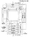
タッチ検出機能付き表示装置1は、制御部11と、ゲートドライバ12と、ソースドライバ13と、駆動信号生成部15と、駆動電極ドライバ14と、タッチ検出機能付き表示デバイス10と、タッチ検出部40とを備えている。
The display device with a
制御部11は、外部より供給された映像信号Vdispに基づいて、ゲートドライバ12、ソースドライバ13、駆動信号生成部15、駆動電極ドライバ14、およびタッチ検出部40に対してそれぞれ制御信号を供給し、これらがお互いに同期して動作するように制御するものである。
The
ゲートドライバ12は、制御部11から供給される制御信号に基づいて、タッチ検出機能付き表示デバイス10の表示駆動の対象となる1水平ラインを順次選択する機能を有している。具体的には、ゲートドライバ12は、後述するように、走査信号Vscanを、走査信号線GCLを介して、画素PixのTFT素子Trのゲートに印加することにより、タッチ検出機能付き表示デバイス10の液晶表示デバイス20にマトリックス状に形成されている画素Pixのうちの1行(1水平ライン)を表示駆動の対象として順次選択するようになっている。
The
ソースドライバ13は、制御部11から供給される制御信号に基づいて、タッチ検出機能付き表示デバイス10の各画素Pix(後述)に画素信号Vpixを供給するものである。具体的には、ソースドライバ13は、後述するように、画素信号Vpixを、画素信号線SGLを介して、ゲートドライバ12により順次選択される1水平ラインを構成する各画素Pixにそれぞれ供給するようになっている。
The
駆動信号生成部15は、制御部11から供給される制御信号に基づいて、駆動信号Vcomを生成するものである。具体的には、駆動信号生成部15は、後述するように、表示動作の為の表示駆動信号Vcomd、およびタッチ検出動作の為のタッチ検出駆動信号Vcomtを生成し、後述する駆動電極ドライバ14に供給するものである。
The drive
駆動電極ドライバ14は、制御部11から供給される制御信号に基づいて、タッチ検出機能付き表示デバイス10の駆動電極COML(後述)に、駆動信号生成部15から供給された駆動信号Vcomを供給するものである。具体的には、駆動電極ドライバ14は、駆動電極COMLに対して、表示駆動信号Vcomdおよびタッチ検出駆動信号Vcomtを時分割的に順次印加する機能を有している。
The
ゲートドライバ13および駆動電極ドライバ14は、走査駆動部50を構成する。走査駆動部50の構成については、後ほど詳細に説明する。
The
タッチ検出機能付き表示デバイス10は、タッチ検出機能を内蔵した表示デバイスである。タッチ検出機能付き表示デバイス10は、液晶表示デバイス20と、タッチ検出デバイス30とを有する。液晶表示デバイス20は、ゲートドライバ12から供給される走査信号Vscanおよび駆動電極ドライバ14から供給される表示駆動信号Vcomdに従って、1水平ラインずつ順次走査して表示を行うデバイスである。タッチ検出デバイス30は、上述した静電容量式タッチ検出の基本原理に基づいて動作するものであり、駆動電極ドライバ14から供給されるタッチ検出駆動信号Vcomtに基づいて、タッチ検出信号Vdetを出力するものである。
The
タッチ検出部40は、制御部11から供給される制御信号と、タッチ検出機能付き表示デバイス10のタッチ検出デバイス30から供給されたタッチ検出信号Vdetに基づいて、タッチ検出デバイス30に対するタッチの有無を検出し、タッチがある場合においてタッチ検出領域におけるその座標などを求める回路である。このタッチ検出部40はアナログLPF(Low Pass Filter)部42と、A/D変換部43と、信号処理部44と、座標抽出部45と、検出タイミング制御部46とを有している。アナログLPF部42は、タッチ検出デバイス30から供給されるタッチ検出信号Vdetに含まれる高い周波数成分(ノイズ成分)を除去し、タッチ成分を取り出してそれぞれ出力する低域通過アナログフィルタである。アナログLPF部42の入力端子のそれぞれと接地との間には、直流電位(0V)を与えるための抵抗Rが接続されている。なお、この抵抗Rに代えて、例えばスイッチを設け、所定の時間にこのスイッチをオン状態にすることにより直流電位(0V)を与えるようにしてもよい。A/D変換部43は、アナログLPF部42から出力されるアナログ信号をそれぞれデジタル信号に変換する回路である。信号処理部44は、A/D変換部43の出力信号に基づいて、タッチ検出デバイス30におけるタッチの有無を検出する論理回路である。座標抽出部45は、信号処理部44においてタッチ検出がなされたときに、そのタッチパネル座標を求める論理回路である。検出タイミング制御部46は、これらの回路が同期して動作するように制御するようになっている。
The
(タッチ検出機能付き表示デバイス10)
次に、タッチ検出機能付き表示デバイス10の構成例を詳細に説明する。
(Display device with touch detection function 10)
Next, a configuration example of the
図5は、タッチ検出機能付き表示デバイス10の要部断面構造の例を表すものである。このタッチ検出機能付き表示デバイス10は、画素基板2と、この画素基板2に対向して配置された対向基板3と、画素基板2と対向基板3との間に挿設された液晶層6とを備えている。
FIG. 5 illustrates an example of a cross-sectional structure of a main part of the
画素基板2は、回路基板としてのTFT基板21と、このTFT基板21上にマトリックス状に配設された複数の画素電極22とを有する。TFT基板21には、図示していないものの、各画素の薄膜トランジスタ(TFT;Thin Film Transistor)や、各画素電極22に画像信号Vpixを供給する画素信号線SGL、各TFTを駆動する走査信号線GCL等の配線が形成されている。
The
対向基板3は、ガラス基板31と、このガラス基板31の一方の面に形成されたカラーフィルタ32と、このカラーフィルタ32の上に形成された複数の駆動電極COMLとを有する。カラーフィルタ32は、例えば赤(R)、緑(G)、青(B)の3色のカラーフィルタ層を周期的に配列して構成したもので、各表示画素にR、G、Bの3色が1組として対応付けられている。駆動電極COMLは、液晶表示デバイス20の共通駆動電極として機能するとともに、タッチ検出デバイス30の駆動電極としても機能するものである。駆動電極COMLは、図示しないコンタクト導電柱によって画素基板2と連結され、このコンタクト導電柱を介して、画素基板2から駆動電極COMLに交流矩形波形の駆動信号Vcom(表示駆動信号Vcomdおよびタッチ検出駆動信号Vcomt)が印加されるようになっている。ガラス基板31の他方の面には、タッチ検出デバイス30の検出電極であるタッチ検出電極TDLが形成され、さらに、このタッチ検出電極TDLの上には、偏光板35が配設されている。
The counter substrate 3 includes a
液晶層6は、電界の状態に応じてそこを通過する光を変調するものであり、例えば、TN(ツイステッドネマティック)、VA(垂直配向)、ECB(電界制御複屈折)等の各種モードの液晶が用いられる。 The liquid crystal layer 6 modulates light passing therethrough according to the state of the electric field. For example, liquid crystal in various modes such as TN (twisted nematic), VA (vertical alignment), and ECB (electric field control birefringence). Is used.
なお、液晶層6と画素基板2との間、および液晶層6と対向基板3との間には、それぞれ配向膜が配設され、また、画素基板2の下面側には入射側偏光板が配置されるが、ここでは図示を省略している。
An alignment film is provided between the liquid crystal layer 6 and the
図6は、液晶表示デバイス20における画素構造の構成例を表すものである。液晶表示デバイス20は、マトリックス状に配列した複数の画素Pixを有している。画素Pixは、TFT素子Trおよび液晶素子LCを有している。TFT素子Trは、薄膜トランジスタにより構成されるものであり、この例では、nチャネルのMOS(Metal Oxide Semiconductor)型のTFTで構成されている。TFT素子Trのソースは画素信号線SGLに接続され、ゲートは走査信号線GCLに接続され、ドレインは液晶素子LCの一端に接続されている。液晶素子LCは、一端がTFT素子Trのドレインに接続され、他端が駆動電極COMLに接続されている。
FIG. 6 illustrates a configuration example of a pixel structure in the liquid
画素Pixは、走査信号線GCLにより、液晶表示デバイス20の同じ行に属する他の画素Pixと互いに接続されている。走査信号線GCLは、ゲートドライバ12と接続され、ゲートドライバ12より走査信号Vscanが供給されるようになっている。画素Pixは、画素信号線SGLにより、液晶表示デバイス20の同じ列に属する他の画素Pixと互いに接続されている。画素信号線SGLは、ソースドライバ13と接続され、ソースドライバ13より画素信号Vpixが供給されるようになっている。
The pixel Pix is connected to another pixel Pix belonging to the same row of the liquid
さらに、画素Pixは、駆動電極COMLにより、液晶表示デバイス20の同じ行に属する他の画素Pixと互いに接続されている。駆動電極COMLは、駆動電極ドライバ14と接続され、駆動電極ドライバ14より駆動信号Vcomが供給されるようになっている。
Further, the pixel Pix is connected to another pixel Pix belonging to the same row of the liquid
この構成により、液晶表示デバイス20では、ゲートドライバ12が走査信号線GCLを時分割的に線順次走査するように駆動することにより、1水平ラインが順次選択され、その1水平ラインに属する画素Pixに対して、ソースドライバ13が画素信号Vpixを供給することにより、1水平ラインずつ表示が行われるようになっている。この表示動作を行う際、駆動電極ドライバ14は、その1水平ラインに対応する駆動電極COMLに対して表示駆動信号Vcomdを印加するようになっている。
With this configuration, in the liquid
図7は、タッチ検出デバイス30の一構成例を斜視的に表すものである。タッチ検出デバイス30は、対向基板3に設けられた、駆動電極COMLおよびタッチ検出電極TDLにより構成されている。駆動電極COMLは、図の左右方向に延在する複数のストライプ状の電極パターンに分割されている。タッチ検出動作を行う際は、各電極パターンには、駆動電極ドライバ14によってタッチ検出駆動信号Vcomtが順次供給され、走査駆動が行われるようになっている。タッチ検出電極TDLは、駆動電極COMLの電極パターンの延在方向と直交する方向に延びるストライプ状の電極パターンから構成されている。タッチ検出電極TDLの各電極パターンは、タッチ検出部40のアナログLPF部42の入力にそれぞれ接続されている。駆動電極COMLとタッチ検出電極TDLにより互いに交差した電極パターンは、その交差部分に静電容量を形成している。
FIG. 7 is a perspective view illustrating a configuration example of the
この構成により、タッチ検出デバイス30では、タッチ検出動作を行う際、駆動電極ドライバ14が駆動電極COMLを時分割的に順次走査するように駆動し、タッチ検出電極TDLからタッチ検出信号Vdetを出力することにより、タッチ検出が行われるようになっている。つまり、駆動電極COMLは、図1〜図3に示したタッチ検出の基本原理における駆動電極E1に対応し、タッチ検出電極TDLは、タッチ検出電極E2に対応するものであり、タッチ検出デバイス30はこの基本原理に従ってタッチを検出するようになっている。図7に示したように、互いに交差した電極パターンは、静電容量式タッチセンサをマトリックス状に構成している。よって、タッチ検出デバイス30のタッチ検出面全体にわたって走査することにより、外部近接物体の接触または近接が生じた位置の検出も可能となっている。
With this configuration, when performing a touch detection operation, the
(走査駆動部50)
次に、ゲートドライバ12および駆動電極ドライバ14により構成される走査駆動部50の構成例を詳細に説明する。
(Scanning drive unit 50)
Next, a configuration example of the scan driving unit 50 including the
図8は、走査駆動部50の一構成例を表すものである。走査駆動部50は、走査制御部51と、表示走査部52と、タッチ検出走査部53と、駆動部540とを備えている。表示走査部52と、走査制御部51および駆動部540の一部はゲートドライバ12を構成している。また、タッチ検出走査部53と、走査制御部51および駆動部540の一部は駆動電極ドライバ14を構成している。駆動部540は、N個の駆動部54(1)〜54(N)から構成されている。以後、N個の駆動部54(1)〜54(N)のうちの任意の一つをさす場合には、単に駆動部54を用いるものとする。
FIG. 8 illustrates a configuration example of the scan driving unit 50. The scan driver 50 includes a scan controller 51, a
走査制御部51は、制御部11より供給された図示しない制御信号に基づいて、表示走査部52およびタッチ検出走査部53に対してそれぞれ制御信号を供給するものである。
The scanning control unit 51 supplies control signals to the
表示走査部52は、シフトレジスタを含んで構成され、走査信号Vscanを順次印加する走査信号線GCLを選択するための信号Sdを生成するものである。また、この信号Sdは、表示駆動信号Vcomdを順次印加する駆動電極COMLを選択するためにも用いられるようになっている。具体的には、表示走査部52は、それぞれが各走査信号線GCLに対応する複数の信号Sdを生成する。そして、表示走査部52が高レベルの信号をn番目の信号Sd(n)として出力したときに、対応するn番目の駆動部54(n)は、n行目の走査信号線GCLに走査信号Vscan(n)を印加するととともに、n行目の駆動電極COML(n)に表示駆動信号Vcomdを印加するようになっている。すなわち、表示走査部52は、高レベルの信号Sdを出力することにより、駆動部540に対して表示駆動を指示するものである。
The
タッチ検出走査部53は、シフトレジスタを含んで構成され、タッチ検出駆動信号Vcomtを順次印加する駆動電極COMLを選択するための信号Stを生成するものである。具体的には、タッチ検出走査部53は、それぞれが各駆動電極COMLに対応する複数の信号Stを生成する。そして、タッチ検出走査部53が高レベルの信号をn番目の信号St(n)として出力したときに、対応するn番目の駆動部54(n)は、n行目の駆動電極COML(n)に対してタッチ検出駆動信号Vcomtを印加するようになっている。すなわち、タッチ検出走査部53は、高レベルの信号Stを出力することにより、駆動部540に対してタッチ検出駆動を指示するものである。
The touch
駆動部540は、表示走査部52から供給された信号Sdおよびタッチ検出走査部53から供給された信号Stに基づいて、走査信号Vscanを走査信号線GCLに印加するとともに、駆動信号Vcomを駆動電極COMLに印加するものである。駆動部54は、表示走査部51およびタッチ検出走査部52の出力信号の組に対応して1つずつ設けられており、対応する走査信号線GCLに対して走査信号Vscanを印加するとともに、対応する駆動電極COMLに対して駆動信号Vcomを印加するようになっている。駆動部54は、ゲートバッファ55と、駆動信号制御回路56と、駆動信号バッファ57とを備えている。
The driving unit 540 applies the scanning signal Vscan to the scanning signal line GCL based on the signal Sd supplied from the
ゲートバッファ55は、表示走査部52から供給された信号Sdに基づいて、走査信号線GCLに走査信号Vscanを印加する回路である。具体的には、ゲートバッファ55は、信号Sdを、液晶表示デバイス20のTFT素子Trをオンオフ制御することができる振幅レベルに増幅する機能を有している。
The
駆動信号制御回路56は、表示走査部52から供給された信号Sdおよびタッチ検出走査部53から供給された信号Stに基づいて、駆動電極COMLに対する駆動信号Vcomの印加を制御する機能を有している。駆動信号バッファ57は、駆動信号制御回路56から供給された信号に基づいて、駆動電極COMLに駆動信号Vcomを印加する回路である。
The drive
図9は、駆動信号制御回路56および駆動信号バッファ57の一構成例を表すものである。
FIG. 9 shows an example of the configuration of the drive
駆動信号制御回路56は、インバータ62,63と、論理積回路64と、反転論理和回路65とを備えている。インバータ62は、入力された信号Sd(n)の反転論理を生成して出力するものであり、インバータ63は、インバータ62の出力信号の反転論理を生成して信号Seldとして出力するものである。論理積回路64は、信号St(n)およびインバータ62の出力信号の論理積(AND)を生成して信号Seltとして出力するものである。反転論理和回路65は、インバータ63の出力信号Seldおよび論理積回路64の出力信号Seltの反転論理和(NOR)を生成して信号Seldcとして出力するようになっている。
The drive
図10は、駆動信号制御回路56の真理値表を表すものである。この真理値表は、信号Sd(n),St(n)を入力したときの出力信号Seld,Seldc,Seltの論理を示している。
FIG. 10 shows a truth table of the drive
駆動信号制御回路56では、図10に示したように、信号Sd(n)が高レベルであり、かつ信号St(n)が低レベルの場合には、出力信号Seldが高レベルになるとともに、出力信号Seldc,Seltが低レベルになる。信号St(n)が高レベルであり、かつ信号Sd(n)が低レベルの場合には、出力信号Seltが高レベルになるとともに、出力信号Seld,Seldcが低レベルになる。信号Sd(n),St(n)がともに高レベルの場合、出力信号Seldが高レベルになるとともに、出力信号Seldc,Seltが低レベルになる。そして、信号Sd(n),St(n)がともに低レベルの場合、出力信号Seldcが高レベルになるとともに、出力信号Seld,Seltが低レベルになる。
In the drive
駆動信号バッファ57は、バッファ66〜68と、スイッチSW1〜SW3とを備えている。バッファ66は、入力された信号Seldを、スイッチSW1をオンオフ制御することができる振幅レベルに増幅する機能を有している。スイッチSW1は、バッファ66から供給される信号に基づいてオンオフ制御されるものであり、一端には表示駆動信号Vcomdが供給され、他端は駆動信号バッファ57の出力端子に接続されている。バッファ67は、入力された信号Seldcを、スイッチSW2をオンオフ制御することができる振幅レベルに増幅する機能を有している。スイッチSW2は、バッファ67から供給される信号に基づいてオンオフ制御されるものであり、一端には直流駆動信号Vcomdcが供給され、他端は駆動信号バッファ57の出力端子に接続されている。そして、バッファ68は、入力された信号Seltを、スイッチSW3をオンオフ制御することができる振幅レベルに増幅する機能を有している。スイッチSW3は、バッファ68から供給される信号に基づいてオンオフ制御されるものであり、一端にはタッチ検出駆動信号Vcomtが供給され、他端は駆動信号バッファ57の出力端子に接続されている。
The
図11(A)は表示駆動信号Vcomdを表すものであり、図11(B)はタッチ検出駆動信号Vcomtを表すものであり、図11(C)は直流駆動信号Vcomdcの波形例を表すものである。表示駆動信号Vcomdは、図11(A)に示したように、振幅Vdを有する矩形波信号である。タッチ検出駆動信号Vcomtは、図11(B)に示した例では、表示駆動信号Vcomdと同様の矩形波信号であり、その振幅Vtが表示駆動信号Vcomdよりも大きいものである。直流駆動信号Vcomdcは、図11(C)に示した例では、0Vの直流信号であり、表示駆動信号Vcomdおよびタッチ検出駆動信号Vcomtの電圧波形の時間平均値に等しい電位になっている。 11A shows the display drive signal Vcomd, FIG. 11B shows the touch detection drive signal Vcomt, and FIG. 11C shows a waveform example of the DC drive signal Vcomdc. is there. The display drive signal Vcomd is a rectangular wave signal having an amplitude Vd as shown in FIG. In the example shown in FIG. 11B, the touch detection drive signal Vcomt is a rectangular wave signal similar to the display drive signal Vcomd, and its amplitude Vt is larger than the display drive signal Vcomd. In the example shown in FIG. 11C, the DC drive signal Vcomdc is a DC signal of 0 V, and has a potential equal to the time average value of the voltage waveforms of the display drive signal Vcomd and the touch detection drive signal Vcomt.
この構成により、駆動信号バッファ57は、入力信号Seldが高レベルであり、入力信号Seldc,Seltが低レベルの場合には、表示駆動信号Vcomdを駆動信号Vcom(n)として出力する。また、入力信号Seldcが高レベルであり、入力信号Seld,Seltが低レベルの場合には、直流駆動信号Vcomdcを駆動信号Vcom(n)として出力する。そして、入力信号Seltが高レベルであり、入力信号Seld,Seldcが低レベルの場合には、タッチ検出駆動信号Vcomtを駆動信号Vcom(n)として出力するようになっている。
With this configuration, the
以上の構成により、駆動部54(n)は、表示走査部52から高レベルの信号Sd(n)が供給された場合には、表示駆動の指示と解釈して、駆動電極COML(n)に表示駆動信号Vcomdを印加し、タッチ検出走査部53から高レベルの信号St(n)が供給された場合には、タッチ検出駆動の指示と解釈して、対応する駆動電極COML(n)にタッチ検出駆動信号Vcomtを印加する。また、駆動部54(n)は、表示走査部52から高レベルの信号Sd(n)が供給されるとともに、タッチ検出走査部53から高レベルの信号St(n)が供給された場合には、駆動電極COML(n)に表示駆動信号Vcomdを印加する。つまり、駆動信号制御回路56は、表示駆動とタッチ検出駆動の両方の指示を受けた場合には、表示駆動を優先し、表示駆動の指示と解釈するようになっている。また、駆動部54(n)は、表示走査部52から低レベルの信号Sd(n)が供給されるとともに、タッチ検出走査部53から低レベルの信号St(n)が供給された場合には、表示駆動の指示でもタッチ検出駆動の指示でもないと解釈し、駆動電極COML(n)に直流駆動信号Vcomdcを印加する。
With the above configuration, when the high-level signal Sd (n) is supplied from the
図12は、走査駆動部50の一動作例を表すものである。走査駆動部50は、表示駆動信号Vcomdおよびタッチ検出駆動信号Vcomtを、駆動電極COMLに順次印加する。その際、表示駆動信号Vcomdを印加する対象となる駆動電極COMLと、タッチ検出駆動信号Vcomtを印加する対象となる駆動電極COMLとが重なった場合には(図12(B))、上述した表示駆動を優先するしくみにより、その重なった駆動電極COMLに対して表示駆動信号Vcomdを印加するようになっている。 FIG. 12 illustrates an operation example of the scan driving unit 50. The scan driver 50 sequentially applies the display drive signal Vcomd and the touch detection drive signal Vcomt to the drive electrodes COML. At this time, when the drive electrode COML to which the display drive signal Vcomd is applied and the drive electrode COML to which the touch detection drive signal Vcomt is applied overlap (FIG. 12B), the display described above is performed. The display drive signal Vcomd is applied to the overlapped drive electrode COML by a mechanism that prioritizes driving.
ここで、駆動電極COMLは、本発明における「共通駆動電極」の一具体例に対応する。液晶素子LCは、本発明における「表示素子」の一具体例に対応する。スイッチSW1,SW2,SW3は、本発明における「第1のスイッチ」,「第3のスイッチ」,「第2のスイッチ」の一具体例にそれぞれ対応する。 Here, the drive electrode COML corresponds to a specific example of “common drive electrode” in the present invention. The liquid crystal element LC corresponds to a specific example of “display element” in the invention. The switches SW1, SW2, and SW3 correspond to specific examples of “first switch”, “third switch”, and “second switch” in the present invention, respectively.
[動作および作用]
続いて、本実施の形態のタッチ検出機能付き表示装置1の動作および作用について説明する。
[Operation and Action]
Next, the operation and action of the display device with a
(全体動作概要)
制御部11は、外部より供給された映像信号Vdispに基づいて、ゲートドライバ12、ソースドライバ13、駆動信号生成部15、駆動電極ドライバ14、およびタッチ検出部40に対してそれぞれ制御信号を供給し、これらがお互いに同期して動作するように制御する。ゲートドライバ12は、液晶表示デバイス20に走査信号Vscanを供給し、表示駆動の対象となる1水平ラインを順次選択する。ソースドライバ13は、ゲートドライバ12により選択された、1水平ラインを構成する各画素Pixに、画素信号Vpixを供給する。駆動信号生成部15は、表示動作の為の表示駆動信号Vcomdおよびタッチ検出動作の為のタッチ検出駆動信号Vcomtを生成する。駆動電極ドライバ14は、表示動作では、表示駆動の対象となる1水平ラインに係る駆動電極COMLに表示駆動信号Vcomdを順次印加し、タッチ検出動作では、タッチ検出動作に係る駆動電極COMLに対してタッチ検出駆動信号Vcomtを順次印加する。タッチ検出機能付き表示デバイス10は、ゲートドライバ12、ソースドライバ13、および駆動電極ドライバ14により供給された信号に基づいて表示動作を行うとともに、駆動電極ドライバ14により供給されたタッチ検出駆動信号Vcomtに基づいてタッチ検出動作を行い、タッチ検出電極TDLからタッチ検出信号Vdetを出力する。アナログLPF部42は、タッチ検出信号Vdetの高い周波数成分を除去して出力する。A/D変換部43は、アナログLPF部42から出力されるアナログ信号をデジタル信号に変換する。信号処理部44は、A/D変換部43の出力信号に基づいて、タッチ検出機能付き表示デバイス10に対するタッチの有無を検出する。座標抽出部45は、信号処理部44においてタッチ検出がなされたときに、そのタッチパネル座標を求める。検出タイミング制御部46は、アナログLPF部42、A/D変換部43、信号処理部44、座標抽出部45が同期して動作するように制御する。
(Overview of overall operation)
The
以下に、タッチ検出機能付き表示装置1の詳細動作を説明する。
Below, detailed operation | movement of the
(表示動作およびタッチ検出動作)
図13は、タッチ検出機能付き表示装置1の表示動作およびタッチ検出動作の一例を表すものであり、(A)は表示駆動信号Vcomdの波形を示し、(B)はタッチ検出駆動信号Vcomtの波形を示し、(C)は駆動信号Vcomの波形を示し、(D)は走査信号Vscanの波形を示し、(E)は画素信号Vpixの波形を示し、(F)はタッチ検出信号Vdetの波形を示す。この例は、図13(C)に示したように、(n−2)行目から(n+2)行目の駆動電極COML(n-2)〜COML(n+2)が表示駆動の対象として順次選択されるとともに、(k−4)行目から(k+5)行目の駆動電極COML(k-4)〜COML(k+5)がタッチ検出駆動の対象として順次選択される場合を示している。
(Display operation and touch detection operation)
13A and 13B show an example of the display operation and the touch detection operation of the
タッチ検出機能付き表示装置1では、表示動作においては、ゲートドライバ12が、走査信号線GCLに対して走査信号Vscanを印加し(図13(D))、駆動電極ドライバ14が、その走査信号線GCLに対応する駆動電極COMLに対して表示駆動信号Vcomdを順次印加することにより表示走査を行う(図13(C)における駆動信号Vcom(n-2)〜Vcom(n+2))。そして各1水平期間(1H)では、走査信号Vscanおよび表示駆動信号Vcomdが印加された1水平ラインに対してソースドライバ13が画素信号Vpixを供給することにより、その1水平ラインの表示が行われる。また、タッチ検出動作においては、駆動電極ドライバ14が、この例では6本の駆動電極COMLに対して、表示駆動信号Vcomdよりも振幅が大きいタッチ検出駆動信号Vcomtを印加し(図13(C)における駆動信号Vcom(k-4)〜Vcom(k+5))、そのタッチ検出駆動信号Vcomtを印加する駆動電極COMLを1水平期間ごとに2本ずつシフトすることによりタッチ検出走査を行う。つまり、表示走査とタッチ検出走査は独立して行われる。各1水平期間(1H)では、タッチ検出部40が、タッチ検出信号Vdetに基づいてタッチを検出する。以下に、その詳細を説明する。
In the
まず、駆動電極ドライバ14は、タイミングt1において、駆動電極COMLに対して駆動信号Vcomを印加する。具体的には、駆動電極ドライバ14は、(n−1)行目の駆動電極COML(n-1)に対して表示駆動信号Vcomd(駆動信号Vcom(n-1))を印加する(図13(C))。同時に、この駆動電極ドライバ14は、(k−4)行目から(k+1)行目の6本の駆動電極COML(k-4)〜COML(k+1)に対してタッチ検出駆動信号Vcomt(駆動信号Vcom(k-4)〜Vcom(k+1))を印加する(図13(C))。これにより、1水平期間(1H)が開始する。このとき、この表示駆動信号Vcomdおよびタッチ検出駆動信号Vcomtは、静電容量を介してタッチ検出電極TDLに伝わり、タッチ検出信号Vdetが変化する(図13(F))。
First, the
次に、ゲートドライバ12は、タイミングt2において、(n−1)行目の走査信号線GCL(n-1)に対して走査信号Vscanを印加し、走査信号Vscan(n-1)が低レベルから高レベルに変化する(図13(D))。
Next, the
次に、ソースドライバ13は、タイミングt3において、画素信号線SGLに対して画素信号Vpixを印加し(図13(E))、1水平ラインに対する表示を行う。ソースドライバ13による画素信号Vpixの供給が終了したのち、ゲートドライバ12は、(n−1)行目の走査信号線GCL(n-1)の走査信号Vscan(n-1)を高レベルから低レベルに変化させる(図13(D))。
Next, the
次に、A/D変換部43は、サンプリングタイミングts1において、タッチ検出信号Vdetが入力されたアナログLPF部42の出力信号をA/D変換する(図13(F))。
Next, the A / D conversion unit 43 performs A / D conversion on the output signal of the
次に、駆動電極ドライバ14は、タイミングt11において、駆動電極COMLに対して駆動信号Vcomを印加する。具体的には、駆動信号生成部15は、表示駆動信号Vcomdを反転させ(図13(A))、駆動電極ドライバ14は、n行目の駆動電極COML(n)に対してその表示駆動信号Vcomd(駆動信号Vcom(n))を印加する(図13(C))。同時に、駆動信号生成部15は、タッチ検出駆動信号Vcomtを反転させ(図13(B))、駆動電極ドライバ14は、(k−2)行目から(k+3)行目の6本の駆動電極COML(k-2)〜COML(k+3)に対してタッチ検出駆動信号Vcomt(駆動信号Vcom(k-2)〜Vcom(k+3))を印加する(図13(C))。これにより、次の1水平期間(1H)が開始する。このとき、この表示駆動信号Vcomdおよびタッチ検出駆動信号Vcomtは、静電容量を介してタッチ検出電極TDLに伝わり、タッチ検出信号Vdetが変化する(図13(F))。
Next, the
次に、A/D変換部43は、サンプリングタイミングts2において、タッチ検出信号Vdetが入力されたアナログLPF部42の出力信号をA/D変換する(図13(F))。タッチ検出部40の信号処理部44では、サンプリングタイミングts1におけるA/D変換結果と、サンプリングタイミングts2におけるA/D変換結果の差に基づいて、タッチ検出を行う。
Next, the A / D conversion unit 43 performs A / D conversion on the output signal of the
次に、ゲートドライバ12が、タイミングt12において、n行目の走査信号線GCL(n)に対して走査信号Vscanを印加し、走査信号Vscan(n)が低レベルから高レベルに変化した後(図13(D))、ソースドライバ13が、タイミングt13において、画素信号線SGLに対して画素信号Vpixを印加する(図13(E))。なお、この例では、タッチ検出機能付き表示装置1は反転駆動を行うため、ソースドライバ13が印加する画素信号Vpixは、一つ前の1水平期間のものと比べて、その極性が反転している。ソースドライバ13による画素信号Vpixの供給が終了したのち、ゲートドライバ12は、n行目の走査信号線GCL(n)の走査信号Vscan(n)を高レベルから低レベルに変化させる(図13(D))。
Next, after the
これ以降、上述した動作を繰り返すことにより、タッチ検出機能付き表示装置1は、液晶表示デバイス20の全面にわたり順次走査することによりその全面に対する表示動作を行うとともに、タッチ検出デバイス30の全面にわたり順次走査することによりその全面に対するタッチ検出動作を行う。
Thereafter, by repeating the above-described operation, the display device with a
このように、タッチ検出機能付き表示装置1では、タッチ検出駆動信号Vcomtの振幅Vtを、表示駆動信号Vcomdの振幅Vdよりも大きくしたので、表示駆動信号Vcomdをタッチ検出駆動信号としても共用する場合に比べて、タッチ検出信号Vdetの電圧変化量を大きくすることができ、タッチ検出感度を高めることができる。
As described above, in the
以上に示したように、タッチ検出機能付き表示装置1では、表示走査とタッチ検出走査とは、互いに独立して行われるため、表示駆動の対象に係る駆動電極COMLと、タッチ検出駆動の対象に係る駆動電極COMLが重なる場合がある。このとき、タッチ検出機能付き表示装置1では、駆動部54が表示駆動を優先する。以下に駆動部54の動作を説明する。
As described above, in the
(駆動部54の詳細動作)
図14は、駆動部54(n)の一動作例を表すものであり、(A)は表示駆動信号Vcomdの波形を示し、(B)はタッチ検出駆動信号Vcomtの波形を示し、(C)は直流駆動信号Vcomdcの波形を示し、(D)は信号Sd(n)の波形を示し、(E)は信号St(n)の波形を示し、(F)は走査信号Vscan(n)の波形を示し、(G)は駆動信号Vcom(n)の波形を示す。
(Detailed operation of the drive unit 54)
FIG. 14 illustrates an operation example of the drive unit 54 (n), where (A) illustrates the waveform of the display drive signal Vcomd, (B) illustrates the waveform of the touch detection drive signal Vcomt, and (C). Indicates the waveform of the DC drive signal Vcomdc, (D) indicates the waveform of the signal Sd (n), (E) indicates the waveform of the signal St (n), and (F) indicates the waveform of the scanning signal Vscan (n). (G) shows the waveform of the drive signal Vcom (n).
表示動作では、駆動部54は、表示走査部52が出力する信号Sdに基づいて、走査信号線GCLに対して走査信号Vscanを印加するとともに、駆動電極COMLに対して表示駆動信号Vcomdを印加する。タッチ検出動作では、駆動部54は、タッチ検出走査部53が出力する信号Stに基づいて、駆動電極COMLに対してタッチ検出駆動信号Vcomtを印加する。表示駆動の対象に係る駆動電極COMLと、タッチ検出駆動の対象に係る駆動電極COMLが重なった場合には、駆動部54は、その駆動電極COMLに対して表示駆動信号Vcomdを印加する。以下に、その詳細を説明する。
In the display operation, the driving
駆動部54(n)は、表示走査部52から高レベルの信号Sd(n)が供給されたとき、タイミングt21〜t22に示したように、走査信号Vscan(n)を高レベルにするとともに(図14(F))、表示駆動信号Vcomdを駆動信号Vcom(n)として出力する(図14(G))。具体的には、ゲートバッファ55は、供給された信号Sd(n)を増幅して、走査信号Vscan(n)として出力する(図14(F))。また、駆動信号制御回路56は、高レベルの信号Sd(n)と低レベルの信号St(n)により、表示駆動の指示と解釈し、駆動信号バッファ57が、表示駆動信号Vcomd(図14(A))を駆動信号Vcom(n)として出力する(図14(G))。
When the high level signal Sd (n) is supplied from the
駆動部54(n)は、タッチ検出走査部53から高レベルの信号St(n)が供給されたとき、タイミングt31〜t34に示したように、タッチ検出駆動信号Vcomtを駆動信号Vcom(n)として出力する(図14(G))。具体的には、駆動信号制御回路56は、高レベルの信号St(n)と低レベルの信号Sd(n)により、タッチ検出駆動の指示と解釈し、駆動信号バッファ57が、タッチ検出駆動信号Vcomt(図14(B))を駆動信号Vcom(n)として出力する(図14(G))。
When the high-level signal St (n) is supplied from the touch
駆動部54(n)は、表示走査部52から高レベルの信号Sd(n)が供給されるとともに、タッチ検出走査部53から高レベルの信号St(n)が供給されたとき、走査信号Vscan(n)を高レベルにするとともに(図14(F))、表示駆動信号Vcomdを駆動信号Vcom(n)として出力する(図14(G))。具体的には、まずタイミングt41において、信号St(n)が高レベルになったとき、高レベルの信号St(n)と低レベルの信号Sd(n)により、駆動信号制御回路56がタッチ検出駆動の指示と解釈し、駆動信号バッファ57がタッチ検出駆動信号Vcomt(図14(B))を駆動信号Vcom(n)として出力する(図14(G))。次に、タイミングt42において、信号Sd(n)が高レベルになったとき、高レベルの信号St(n)と高レベルの信号Sd(n)により、駆動信号制御回路56が表示駆動の指示と解釈し、駆動信号バッファ57が表示駆動信号Vcomd(図14(A))を駆動信号Vcom(n)として出力する(図14(G))。すなわち、駆動信号制御回路56は、表示駆動とタッチ検出駆動の両方の指示を受けた場合には、表示駆動を優先することにより、表示駆動の指示と解釈する。次に、タイミングt43において、信号Sd(n)が低レベルになったとき、高レベルの信号St(n)と低レベルの信号Sd(n)により、駆動信号制御回路56がタッチ検出駆動の指示と解釈し、駆動信号バッファ57がタッチ検出駆動信号Vcomt(図14(B))を駆動信号Vcom(n)として出力する(図14(G))。
The drive unit 54 (n) is supplied with the high level signal Sd (n) from the
このように、タッチ検出機能付き表示装置1では、表示駆動の対象に係る駆動電極COMLと、タッチ検出駆動の対象に係る駆動電極COMLが重なった場合には、駆動部54は、表示駆動を優先し、その駆動電極COMLに対して表示駆動信号Vcomdを印加する。言い換えれば、ソースドライバ13が画素信号Vpixを印加している水平ラインに係る駆動電極COMLには、表示駆動信号Vcomdが印加され、タッチ検出駆動信号Vcomtが印加されることはない。これにより、表示の乱れを低減することができる。
Thus, in the
[効果]
以上のように、本実施の形態では、駆動電極に対して、表示駆動信号とタッチ検出駆動信号とを別々に供給できるようにしたので、タッチ検出駆動信号の振幅を表示駆動信号の振幅よりも大きくすることができ、タッチ検出の検出感度を高めることができる。
[effect]
As described above, in the present embodiment, the display drive signal and the touch detection drive signal can be separately supplied to the drive electrodes, so that the amplitude of the touch detection drive signal is greater than the amplitude of the display drive signal. The detection sensitivity of touch detection can be increased.
また、本実施の形態では、表示駆動の対象となる駆動電極とタッチ検出駆動の対象となる駆動電極が重なった場合には、表示駆動信号をその重なった駆動電極に印加するようにしたので、表示の乱れを低減することができる。 In the present embodiment, when the drive electrode that is the target of display drive and the drive electrode that is the target of touch detection drive overlap, the display drive signal is applied to the overlapped drive electrode. Display disturbance can be reduced.
また、本実施の形態では、表示駆動信号およびタッチ検出駆動信号をあらかじめ生成しておき、スイッチを切り替えることによりこれらの駆動信号を駆動電極に印加するようにしたので、シンプルな構成で複数の駆動信号を駆動電極に選択的に印加することができる。 In the present embodiment, the display drive signal and the touch detection drive signal are generated in advance, and these drive signals are applied to the drive electrodes by switching the switch. A signal can be selectively applied to the drive electrodes.
上記実施の形態では、走査駆動部50が、6本の駆動電極COMLに対してタッチ検出駆動信号Vcomtを同時に印加したが、これに限定されるものではなく、これに代えて、例えば5本以下もしくは7本以上の駆動電極COMLに対してタッチ検出駆動信号Vcomtを同時に印加してもよい。 In the above embodiment, the scanning drive unit 50 applies the touch detection drive signal Vcomt to the six drive electrodes COML at the same time. However, the present invention is not limited to this, and instead, for example, five or less. Alternatively, the touch detection drive signal Vcomt may be simultaneously applied to seven or more drive electrodes COML.
<3.適用例>
次に、図15〜図19を参照して、上記実施の形態および変形例で説明したタッチ検出機能付き表示装置の適用例について説明する。上記実施の形態等のタッチ検出機能付き表示装置は、テレビジョン装置、デジタルカメラ、ノート型パーソナルコンピュータ、携帯電話等の携帯端末装置あるいはビデオカメラなどのあらゆる分野の電子機器に適用することが可能である。言い換えると、上記実施の形態等のタッチ検出機能付き表示装置は、外部から入力された映像信号あるいは内部で生成した映像信号を、画像あるいは映像として表示するあらゆる分野の電子機器に適用することが可能である。
<3. Application example>
Next, with reference to FIGS. 15 to 19, application examples of the display device with a touch detection function described in the above embodiment and modifications will be described. The display device with a touch detection function according to the above-described embodiments can be applied to electronic devices in various fields such as a television device, a digital camera, a notebook personal computer, a mobile terminal device such as a mobile phone, or a video camera. is there. In other words, the display device with a touch detection function according to the above-described embodiment can be applied to electronic devices in various fields that display an externally input video signal or an internally generated video signal as an image or video. It is.
(適用例1)
図15は、上記実施の形態等のタッチ検出機能付き表示装置が適用されるテレビジョン装置の外観を表すものである。このテレビジョン装置は、例えば、フロントパネル511およびフィルターガラス512を含む映像表示画面部510を有しており、この映像表示画面部510は、上記実施の形態等に係るタッチ検出機能付き表示装置により構成されている。
(Application example 1)
FIG. 15 illustrates an appearance of a television device to which the display device with a touch detection function according to the above-described embodiment or the like is applied. The television apparatus has, for example, a video display screen unit 510 including a front panel 511 and a filter glass 512. The video display screen unit 510 is obtained by the display device with a touch detection function according to the above-described embodiment and the like. It is configured.
(適用例2)
図16は、上記実施の形態等のタッチ検出機能付き表示装置が適用されるデジタルカメラの外観を表すものである。このデジタルカメラは、例えば、フラッシュ用の発光部521、表示部522、メニュースイッチ523およびシャッターボタン524を有しており、その表示部522は、上記実施の形態等に係るタッチ検出機能付き表示装置により構成されている。
(Application example 2)
FIG. 16 illustrates an appearance of a digital camera to which the display device with a touch detection function according to the above-described embodiment or the like is applied. The digital camera includes, for example, a flash
(適用例3)
図17は、上記実施の形態等のタッチ検出機能付き表示装置が適用されるノート型パーソナルコンピュータの外観を表すものである。このノート型パーソナルコンピュータは、例えば、本体531、文字等の入力操作のためのキーボード532および画像を表示する表示部533を有しており、その表示部533は、上記実施の形態等に係るタッチ検出機能付き表示装置により構成されている。
(Application example 3)
FIG. 17 illustrates an appearance of a notebook personal computer to which the display device with a touch detection function according to the above-described embodiment or the like is applied. The notebook personal computer includes, for example, a main body 531, a keyboard 532 for inputting characters and the like, and a display unit 533 for displaying an image. The display unit 533 is a touch according to the above-described embodiment and the like. It is comprised by the display apparatus with a detection function.
(適用例4)
図18は、上記実施の形態等のタッチ検出機能付き表示装置が適用されるビデオカメラの外観を表すものである。このビデオカメラは、例えば、本体部541、この本体部541の前方側面に設けられた被写体撮影用のレンズ542、撮影時のスタート/ストップスイッチ543および表示部544を有している。そして、その表示部544は、上記実施の形態等に係るタッチ検出機能付き表示装置により構成されている。
(Application example 4)
FIG. 18 illustrates an appearance of a video camera to which the display device with a touch detection function according to the above-described embodiment or the like is applied. This video camera has, for example, a main body 541, a subject shooting lens 542 provided on the front side surface of the main body 541, a start /
(適用例5)
図19は、上記実施の形態等のタッチ検出機能付き表示装置が適用される携帯電話機の外観を表すものである。この携帯電話機は、例えば、上側筐体710と下側筐体720とを連結部(ヒンジ部)730で連結したものであり、ディスプレイ740、サブディスプレイ750、ピクチャーライト760およびカメラ770を有している。そのディスプレイ740またはサブディスプレイ750は、上記実施の形態等に係るタッチ検出機能付き表示装置により構成されている。
(Application example 5)
FIG. 19 illustrates an appearance of a mobile phone to which the display device with a touch detection function according to the above-described embodiment or the like is applied. For example, the mobile phone is obtained by connecting an
以上、実施の形態および電子機器への適用例を挙げて本発明を説明したが、本発明はこれらの実施の形態等には限定されず、種々の変形が可能である。 Although the present invention has been described above with reference to the embodiments and application examples to electronic devices, the present invention is not limited to these embodiments and the like, and various modifications are possible.
上記の実施の形態等では、TNやVA、ECB等の各種モードの液晶を用いた液晶表示デバイス20とタッチ検出デバイス30とを一体化してタッチ検出機能付き表示デバイス10を構成したが、これに代えて、FFS(フリンジフィールドスイッチング)やIPS(インプレーンスイッチング)等の横電界モードの液晶を用いた液晶表示デバイスとタッチ検出デバイスとを一体化しても良い。例えば、横電界モードの液晶を用いた場合には、タッチ検出機能付き表示デバイス90を、図20に示したように構成可能である。この図は、タッチ検出機能付き表示デバイス90の要部断面構造の一例を表すものであり、画素基板2Bと対向基板3Bとの間に液晶層6Bを挟持された状態を示している。その他の各部の名称や機能等は図5の場合と同様なので、説明を省略する。この例では、図5の場合とは異なり、表示用とタッチ検出用の双方に兼用される駆動電極COMLは、TFT基板21の直ぐ上に形成され、画素基板2Bの一部を構成する。駆動電極COMLの上方には、絶縁層23を介して画素電極22が配置される。この場合、駆動電極COMLとタッチ検出電極TDLとの間の、液晶層6Bをも含むすべての誘電体が容量C1の形成に寄与する。
In the above embodiment, the liquid
1…タッチ検出機能付き表示装置、2…画素基板、3…対向基板、6…液晶層、10タッチ検出機能付きデバイス、11…制御部、12…ゲートドライバ、13…ソースドライバ、14…駆動電極ドライバ、15…駆動信号生成部、20…液晶表示デバイス、21…TFT基板、22…画素電極、30…タッチ検出デバイス、31…ガラス基板、32…カラーフィルタ、35…偏光板、40…タッチ検出部、42…アナログLPF部、43…A/D変換部、44…信号処理部、45…座標抽出部、46…検出タイミング制御部、50…走査駆動部、51…走査制御部、52…表示走査部、53…タッチ検出走査部、54…駆動部、55…ゲートバッファ、56…駆動信号制御回路、57…駆動信号バッファ、62,63…インバータ、64…論理積回路、65…反転論理和回路、66〜68…バッファ、COML…駆動電極、GCL…走査信号線、LC…液晶素子、Out…出力信号、Pix…画素、Sd,St,Seld,Seldc,Selt…信号、SGL…画素信号線、SW1〜SW3…スイッチ、TDL…タッチ検出電極、Tr…TFT素子、ts1,ts2…サンプリングタイミング、Vcom…駆動信号、Vcomd…表示駆動信号、Vcomdc…直流駆動信号、Vcomt…タッチ検出駆動信号、Vdet…タッチ検出信号、Vdisp…映像信号、Vpix…画素信号、Vscan…走査信号。
DESCRIPTION OF
Claims (7)
前記複数の共通駆動電極と対向してマトリックス状に配設され画素信号および表示駆動信号に基づいて表示を行う複数の画素電極と、
前記複数の共通駆動電極と対向して設けられ前記共通駆動電極との間で静電容量を形成し、前記表示駆動信号よりも大きい振幅を有するタッチ検出駆動信号に基づいて外部近接物体を検出するタッチ検出電極と、
前記表示駆動信号を前記複数の共通駆動電極に時分割的に順次印加する第1の走査駆動と、前記タッチ検出駆動信号を前記複数の共通駆動電極に時分割的に順次印加する第2の走査駆動とを行う走査駆動部と
を備え、
前記走査駆動部は、
一端に前記表示駆動信号が供給され他端が前記共通駆動電極に接続される第1のスイッチと、一端に前記タッチ検出駆動信号が供給され他端が前記共通駆動電極に接続される第2のスイッチと、を有し、
前記第1の走査駆動の対象として選択された共通駆動電極と前記第2の走査駆動の対象として選択された共通駆動電極とが重なる場合には、前記第1のスイッチをオン状態とし、前記第2のスイッチをオフ状態とする
タッチ検出機能付き表示装置。 A plurality of common drive electrodes arranged in parallel to extend in one direction;
A plurality of pixel electrodes arranged in a matrix so as to face the plurality of common drive electrodes and performing display based on pixel signals and display drive signals;
An electrostatic capacitance is formed between the plurality of common drive electrodes and the common drive electrode, and an external proximity object is detected based on a touch detection drive signal having an amplitude larger than the display drive signal. a filter pitch detection electrodes,
A first scan that sequentially applies the display drive signal to the plurality of common drive electrodes in a time-division manner, and a second scan that sequentially applies the touch detection drive signal to the plurality of common drive electrodes in a time-division manner. A scanning drive unit for driving , and
The scan driver is
A first switch in which the display drive signal is supplied to one end and the other end is connected to the common drive electrode, and a second switch in which the touch detection drive signal is supplied to one end and the other end is connected to the common drive electrode A switch,
When the common drive electrode selected as the first scan drive target and the common drive electrode selected as the second scan drive target overlap, the first switch is turned on and the first switch is turned on. A display device with a touch detection function that turns off the switch 2 .
前記走査駆動部は、前記第1および第2の走査駆動の対象として選択されていない共通駆動電極に対して、前記第3のスイッチをオン状態にすることにより、前記直流電位を印加する
請求項1に記載のタッチ検出機能付き表示装置。 The scan driver further includes a third switch is the other end direct current position is supplied to one end is connected to the common driving electrode,
The scanning drive unit applies the DC potential to the common drive electrode that is not selected as the first and second scan drive targets by turning on the third switch. The display device with a touch detection function according to 1.
請求項2に記載のタッチ検出機能付き表示装置。 The display device with a touch detection function according to claim 2 , wherein the DC potential is equal to a time average value of a voltage of the display drive signal.
請求項1に記載のタッチ検出機能付き表示装置。 The display device with a touch detection function according to claim 1 , wherein the touch detection drive signal is a rectangular wave signal whose polarity is inverted.
前記走査駆動部は、
一端に前記表示駆動信号が供給され他端が前記共通駆動電極に接続される第1のスイッチと、一端に前記タッチ検出駆動信号が供給され他端が前記共通駆動電極に接続される第2のスイッチと、を有し、
前記第1の走査駆動の対象として選択された共通駆動電極と前記第2の走査駆動の対象として選択された共通駆動電極とが重なる場合には、前記第1のスイッチをオン状態とし、前記第2のスイッチをオフ状態とする
駆動回路。 A plurality of pixels performing a plurality of common drive electrodes are juxtaposed so as to extend in one direction, a display based on said plurality of common drive electrodes opposed to being arranged in a matrix pixel signal and a display drive signal and the electrode, the plurality of common drive electrodes opposed to provided to form an electrostatic capacitance between said common driving electrode, a filter pitch detection electrodes to detect the external proximity object based on the touch detection drive signal A first scanning drive that sequentially applies the display drive signal to the plurality of common drive electrodes in a time-division manner, and a touch having a larger amplitude than the display drive signal. A scan driver that performs a second scan drive that sequentially applies a detection drive signal to the plurality of common drive electrodes in a time-sharing manner ;
The scan driver is
A first switch in which the display drive signal is supplied to one end and the other end is connected to the common drive electrode, and a second switch in which the touch detection drive signal is supplied to one end and the other end is connected to the common drive electrode A switch,
When the common drive electrode selected as the first scan drive target and the common drive electrode selected as the second scan drive target overlap, the first switch is turned on and the first switch is turned on. 2 is a drive circuit for turning off the switch 2 .
前記表示駆動信号よりも大きい振幅を有するタッチ検出駆動信号を、前記複数の共通駆動電極に時分割的に順次印加することにより、前記複数の共通駆動電極と対向して設けられ前記共通駆動電極との間で静電容量を形成するタッチ検出電極からの検出信号に基づいて外部近接物体を検出する第2の走査駆動動作と
を行い、
前記第1の走査駆動動作の対象として選択された共通駆動電極と前記第2の走査駆動動作の対象として選択された共通駆動電極とが重なる場合には、一端に前記表示駆動信号が供給され他端が前記共通駆動電極に接続される第1のスイッチをオン状態とし、一端に前記タッチ検出駆動信号が供給され他端が前記共通駆動電極に接続される第2のスイッチをオフ状態とする
タッチ検出機能付き表示装置の駆動方法。 A display drive signal is sequentially applied to a plurality of common drive electrodes arranged in parallel so as to extend in one direction in a time-sharing manner, and is opposed to the plurality of common drive electrodes in synchronization with the application of the display drive signal. The pixel signal and the pixel signal and the pixel electrode corresponding to the common drive electrode under the application of the display drive signal among the pixel electrodes arranged in a matrix are sequentially performed in a time-sharing manner. A first scan driving operation for performing display based on the display driving signal;
A touch detection drive signal having a larger amplitude than the display drive signal is sequentially applied to the plurality of common drive electrodes in a time-sharing manner, thereby being provided to face the plurality of common drive electrodes, perform second scanning driving operation of detecting the external proximity object based on a detection signal from the touch detection electrode for forming a capacitance between,
When the common drive electrode selected as the target of the first scan drive operation and the common drive electrode selected as the target of the second scan drive operation overlap, the display drive signal is supplied to one end and the other A touch whose one end is connected to the common drive electrode is turned on, the touch detection drive signal is supplied to one end and the second switch whose other end is connected to the common drive electrode is turned off. A method for driving a display device with a detection function.
前記タッチ検出機能付き表示装置を利用した動作制御を行う制御部と
を備え、
前記タッチ検出機能付き表示装置は、
一方向に延在するように並設された複数の共通駆動電極と、
前記複数の共通駆動電極と対向してマトリックス状に配設され画素信号および表示駆動信号に基づいて表示を行う複数の画素電極と、
前記複数の共通駆動電極と対向して設けられ前記共通駆動電極との間で静電容量を形成し、前記表示駆動信号よりも大きい振幅を有するタッチ検出駆動信号に基づいて外部近接物体を検出するタッチ検出電極と、
前記表示駆動信号を前記複数の共通駆動電極に時分割的に順次印加する第1の走査駆動と、前記タッチ検出駆動信号を前記複数の共通駆動電極に時分割的に順次印加する第2の走査駆動とを行う走査駆動部と
を備え、
前記走査駆動部は、
一端に前記表示駆動信号が供給され他端が前記共通駆動電極に接続される第1のスイッチと、一端に前記タッチ検出駆動信号が供給され他端が前記共通駆動電極に接続される第2のスイッチと、を有し、
前記第1の走査駆動の対象として選択された共通駆動電極と前記第2の走査駆動の対象として選択された共通駆動電極とが重なる場合には、前記第1のスイッチをオン状態とし、前記第2のスイッチをオフ状態とする
電子機器。 A display device with a touch detection function;
A control unit that performs operation control using the display device with a touch detection function,
The display device with a touch detection function is:
A plurality of common drive electrodes arranged in parallel to extend in one direction;
A plurality of pixel electrodes arranged in a matrix so as to face the plurality of common drive electrodes and performing display based on pixel signals and display drive signals;
An electrostatic capacitance is formed between the plurality of common drive electrodes and the common drive electrode, and an external proximity object is detected based on a touch detection drive signal having an amplitude larger than the display drive signal. a filter pitch detection electrodes,
A first scan that sequentially applies the display drive signal to the plurality of common drive electrodes in a time-division manner, and a second scan that sequentially applies the touch detection drive signal to the plurality of common drive electrodes in a time-division manner. A scanning drive unit for driving
With
The scan driver is
A first switch in which the display drive signal is supplied to one end and the other end is connected to the common drive electrode, and a second switch in which the touch detection drive signal is supplied to one end and the other end is connected to the common drive electrode A switch,
When the common drive electrode selected as the first scan drive target and the common drive electrode selected as the second scan drive target overlap, the first switch is turned on and the first switch is turned on. An electronic device that turns off the switch 2 .
Priority Applications (6)
| Application Number | Priority Date | Filing Date | Title |
|---|---|---|---|
| JP2010186199A JP5539106B2 (en) | 2010-08-23 | 2010-08-23 | Display device with touch detection function, drive circuit, driving method of display device with touch detection function, and electronic device |
| US13/067,934 US8933895B2 (en) | 2010-08-23 | 2011-07-08 | Display device with touch detection function, drive circuit, driving method of display device with touch detection function, and electronic unit |
| TW100125686A TWI492129B (en) | 2010-08-23 | 2011-07-20 | Display device with touch detection function, drive circuit, driving method of display device with touch detection function, and electronic unit |
| KR1020110077753A KR101819239B1 (en) | 2010-08-23 | 2011-08-04 | Display device with touch detection function, drive circuit, driving method of display device with touch detection function, and electronic unit |
| CN201110234339.4A CN102375637B (en) | 2010-08-23 | 2011-08-16 | Display device and method, drive circuit and electronic equipment |
| US14/565,192 US20150091868A1 (en) | 2010-08-23 | 2014-12-09 | Display device with touch detention function, drive circuit, driving method of display device with touch detention function, and electronic unit |
Applications Claiming Priority (1)
| Application Number | Priority Date | Filing Date | Title |
|---|---|---|---|
| JP2010186199A JP5539106B2 (en) | 2010-08-23 | 2010-08-23 | Display device with touch detection function, drive circuit, driving method of display device with touch detection function, and electronic device |
Publications (2)
| Publication Number | Publication Date |
|---|---|
| JP2012042862A JP2012042862A (en) | 2012-03-01 |
| JP5539106B2 true JP5539106B2 (en) | 2014-07-02 |
Family
ID=45593663
Family Applications (1)
| Application Number | Title | Priority Date | Filing Date |
|---|---|---|---|
| JP2010186199A Active JP5539106B2 (en) | 2010-08-23 | 2010-08-23 | Display device with touch detection function, drive circuit, driving method of display device with touch detection function, and electronic device |
Country Status (5)
| Country | Link |
|---|---|
| US (2) | US8933895B2 (en) |
| JP (1) | JP5539106B2 (en) |
| KR (1) | KR101819239B1 (en) |
| CN (1) | CN102375637B (en) |
| TW (1) | TWI492129B (en) |
Families Citing this family (50)
| Publication number | Priority date | Publication date | Assignee | Title |
|---|---|---|---|---|
| KR101503103B1 (en) * | 2011-03-25 | 2015-03-17 | 엘지디스플레이 주식회사 | Touch sensor integrated type display and driving method therefrom |
| US9298304B2 (en) * | 2011-10-12 | 2016-03-29 | Htc Corporation | Electronic device and touch-sensing method |
| KR101364075B1 (en) * | 2012-03-14 | 2014-02-20 | 엘지디스플레이 주식회사 | Display device with integrated touch screen |
| KR101981529B1 (en) * | 2012-05-25 | 2019-05-24 | 엘지디스플레이 주식회사 | Touch sensing apparatus and driving method thereofp |
| KR101315227B1 (en) | 2012-05-30 | 2013-10-07 | 엘지디스플레이 주식회사 | Display device with integrated touch screen and method for driving the same |
| JP5979988B2 (en) * | 2012-05-31 | 2016-08-31 | 株式会社ジャパンディスプレイ | Liquid crystal display |
| JP6032794B2 (en) * | 2012-06-08 | 2016-11-30 | 株式会社ジャパンディスプレイ | Liquid crystal display |
| CN102750062B (en) * | 2012-06-29 | 2016-02-10 | 京东方科技集团股份有限公司 | A kind of capacitance type in-cell touch panel and display device |
| CN103543857A (en) * | 2012-07-10 | 2014-01-29 | 瀚宇彩晶股份有限公司 | Driving device and method of touch panel |
| KR101423532B1 (en) * | 2012-08-17 | 2014-07-31 | 세심광전자기술(주) | Driving method for touch screen apparatus of single layer capacitive type |
| JPWO2014041717A1 (en) * | 2012-09-13 | 2016-08-12 | パナソニックIpマネジメント株式会社 | Input device and liquid crystal display device |
| US10073550B2 (en) | 2012-09-20 | 2018-09-11 | Synaptics Incorporated | Concurrent input sensing and display updating |
| TWI472979B (en) * | 2012-10-22 | 2015-02-11 | Superc Touch Coporation | Touch panel device with reconfigurable sensing points and its sensing method |
| JP6022320B2 (en) * | 2012-11-20 | 2016-11-09 | 株式会社ジャパンディスプレイ | Liquid crystal display |
| WO2014083563A2 (en) | 2012-11-27 | 2014-06-05 | N-Trig Ltd. | Detection with a capacitive based digitizer sensor |
| JP6097676B2 (en) * | 2012-12-05 | 2017-03-15 | 株式会社ジャパンディスプレイ | Display device with touch detection function and electronic device |
| JP5778122B2 (en) * | 2012-12-14 | 2015-09-16 | 株式会社ジャパンディスプレイ | Display device with touch detection function and electronic device including the same |
| TWI488083B (en) * | 2013-01-11 | 2015-06-11 | Au Optronics Corp | Method using touch sensing ic to control display driving ic and system using the same |
| JP2014186537A (en) | 2013-03-22 | 2014-10-02 | Japan Display Inc | Display device, and electronic apparatus |
| CN103207720B (en) * | 2013-03-29 | 2015-09-16 | 北京京东方光电科技有限公司 | A kind of control method of touch-control display panel and device and display device |
| KR101575957B1 (en) * | 2013-05-30 | 2015-12-10 | 주식회사 엘지화학 | Display apparatus with touch input function and a method of controlling thereof |
| CN104281306B (en) * | 2013-07-10 | 2018-02-13 | 群创光电股份有限公司 | Touch control display device and its manufacture method |
| JP2015043200A (en) * | 2013-07-22 | 2015-03-05 | 株式会社ジャパンディスプレイ | Touch detection device, and display device and electronic apparatus with touch detection function |
| US9244581B2 (en) * | 2013-09-30 | 2016-01-26 | Synaptics Incorporated | Modulated power supply for reduced parasitic capacitance |
| US9442615B2 (en) | 2013-10-02 | 2016-09-13 | Synaptics Incorporated | Frequency shifting for simultaneous active matrix display update and in-cell capacitive touch |
| KR102203449B1 (en) * | 2013-12-31 | 2021-01-15 | 엘지디스플레이 주식회사 | Display device with integrated touch screen and method for driving thereof |
| TWI522876B (en) * | 2014-01-22 | 2016-02-21 | Sitronix Technology Corp | Drive circuit and its touch device and touch module and manufacturing method |
| US9298309B2 (en) | 2014-04-29 | 2016-03-29 | Synaptics Incorporated | Source driver touch transmitter in parallel with display drive |
| JP6422085B2 (en) * | 2014-05-07 | 2018-11-14 | 富士通クライアントコンピューティング株式会社 | Information processing device |
| JP6185889B2 (en) * | 2014-07-04 | 2017-08-23 | 株式会社ジャパンディスプレイ | Display device and driving method thereof |
| CN104317467B (en) | 2014-11-06 | 2018-01-05 | 京东方科技集团股份有限公司 | A kind of In-cell touch panel and display device |
| TWI534678B (en) * | 2014-11-21 | 2016-05-21 | 業鑫科技顧問股份有限公司 | In-cell touch display device and method of driving the same |
| JP6290449B2 (en) * | 2014-11-28 | 2018-03-07 | シャープ株式会社 | Display device with position input function |
| KR102270988B1 (en) * | 2014-12-26 | 2021-06-30 | 엘지디스플레이 주식회사 | Touch display device and the method for driving the same |
| CN104503618B (en) * | 2014-12-29 | 2017-10-27 | 厦门天马微电子有限公司 | A kind of liquid crystal display device, touch-control scanning means and its driving method |
| KR102257170B1 (en) | 2015-01-05 | 2021-05-27 | 시냅틱스 인코포레이티드 | Time sharing of display and sensing data |
| KR20160116165A (en) * | 2015-03-26 | 2016-10-07 | 삼성디스플레이 주식회사 | Display device |
| TWI554932B (en) * | 2015-05-15 | 2016-10-21 | 晨星半導體股份有限公司 | Touch sensing and display circuit and touch sensing and display control module of touch screen, and method of controlling touch screen |
| WO2016189426A1 (en) | 2015-05-28 | 2016-12-01 | 株式会社半導体エネルギー研究所 | Touch panel |
| JP6879678B2 (en) * | 2015-06-22 | 2021-06-02 | 株式会社半導体エネルギー研究所 | Semiconductor device |
| TWI593943B (en) * | 2015-10-19 | 2017-08-01 | 國立清華大學 | A tunable sensing device |
| KR102404391B1 (en) * | 2015-12-31 | 2022-06-03 | 엘지디스플레이 주식회사 | Display Device Having The Touch Sensor |
| JP2017134249A (en) * | 2016-01-28 | 2017-08-03 | 株式会社ジャパンディスプレイ | Display device |
| US10146388B2 (en) * | 2016-03-08 | 2018-12-04 | Synaptics Incorporated | Capacitive sensing in an LED display |
| KR102535638B1 (en) * | 2016-05-30 | 2023-05-24 | 엘지디스플레이 주식회사 | Display device having sensor screen |
| CN106713904A (en) * | 2016-12-20 | 2017-05-24 | 郑州云海信息技术有限公司 | VGA interface test method, apparatus and system |
| JP6734771B2 (en) * | 2016-12-28 | 2020-08-05 | 株式会社ジャパンディスプレイ | Display device |
| JP7009923B2 (en) * | 2017-10-31 | 2022-01-26 | セイコーエプソン株式会社 | Physical quantity measuring devices, electronic devices and mobile objects |
| KR102522290B1 (en) * | 2018-04-05 | 2023-04-19 | 삼성디스플레이 주식회사 | Display device |
| JP7373755B2 (en) * | 2019-03-20 | 2023-11-06 | パナソニックIpマネジメント株式会社 | Display system, control device and control method |
Family Cites Families (18)
| Publication number | Priority date | Publication date | Assignee | Title |
|---|---|---|---|---|
| US5945973A (en) * | 1995-05-12 | 1999-08-31 | Hitachi, Ltd. | Position reader |
| JP3258216B2 (en) * | 1995-10-24 | 2002-02-18 | アルプス電気株式会社 | Liquid crystal display with tablet |
| JPH1091329A (en) | 1996-09-19 | 1998-04-10 | Sony Corp | Information processor and information input method |
| KR20110058895A (en) * | 2006-06-09 | 2011-06-01 | 애플 인크. | Touch screen liquid crystal display |
| KR101246830B1 (en) * | 2006-06-09 | 2013-03-28 | 삼성디스플레이 주식회사 | Display device and method of driving the same |
| KR101251999B1 (en) * | 2006-06-13 | 2013-04-08 | 삼성디스플레이 주식회사 | Liquid crystal display device, and driving method thereof |
| KR101337262B1 (en) * | 2007-02-12 | 2013-12-05 | 삼성디스플레이 주식회사 | Display device and driving method thereof |
| JP4400637B2 (en) | 2007-03-06 | 2010-01-20 | セイコーエプソン株式会社 | Liquid crystal device, driving method of liquid crystal device, and electronic apparatus |
| JP5481040B2 (en) | 2008-04-11 | 2014-04-23 | 株式会社ジャパンディスプレイ | Display device and driving method thereof |
| JP2010055453A (en) | 2008-08-29 | 2010-03-11 | Nissha Printing Co Ltd | Simultaneous multipoint detection method for touch panel, and touch panel device with simultaneous multipoint detection function |
| JP5216495B2 (en) | 2008-09-16 | 2013-06-19 | 株式会社ジャパンディスプレイウェスト | Contact detection device and display device |
| JP5067763B2 (en) | 2008-10-08 | 2012-11-07 | 株式会社ジャパンディスプレイウェスト | Contact detection device, display device, and contact detection method |
| KR100951380B1 (en) | 2008-11-07 | 2010-04-08 | 이성호 | Touch panel |
| US8922521B2 (en) * | 2009-02-02 | 2014-12-30 | Apple Inc. | Switching circuitry for touch sensitive display |
| JP5439467B2 (en) | 2009-02-27 | 2014-03-12 | 株式会社ジャパンディスプレイ | Display device, touch panel, and electronic device |
| JP2011233019A (en) * | 2010-04-28 | 2011-11-17 | Sony Corp | Display device with touch detection function, drive circuit, drive system, and electronic equipment |
| JP5670124B2 (en) * | 2010-08-23 | 2015-02-18 | 株式会社ジャパンディスプレイ | Display device with touch detection function, drive circuit, driving method of display device with touch detection function, and electronic device |
| JP5501158B2 (en) * | 2010-08-23 | 2014-05-21 | 株式会社ジャパンディスプレイ | Display device with touch detection function, drive circuit, driving method of display device with touch detection function, and electronic device |
-
2010
- 2010-08-23 JP JP2010186199A patent/JP5539106B2/en active Active
-
2011
- 2011-07-08 US US13/067,934 patent/US8933895B2/en active Active
- 2011-07-20 TW TW100125686A patent/TWI492129B/en active
- 2011-08-04 KR KR1020110077753A patent/KR101819239B1/en active IP Right Grant
- 2011-08-16 CN CN201110234339.4A patent/CN102375637B/en active Active
-
2014
- 2014-12-09 US US14/565,192 patent/US20150091868A1/en not_active Abandoned
Also Published As
| Publication number | Publication date |
|---|---|
| CN102375637A (en) | 2012-03-14 |
| KR101819239B1 (en) | 2018-02-28 |
| KR20120018716A (en) | 2012-03-05 |
| US8933895B2 (en) | 2015-01-13 |
| JP2012042862A (en) | 2012-03-01 |
| TWI492129B (en) | 2015-07-11 |
| TW201211873A (en) | 2012-03-16 |
| US20150091868A1 (en) | 2015-04-02 |
| CN102375637B (en) | 2016-06-29 |
| US20120044195A1 (en) | 2012-02-23 |
Similar Documents
| Publication | Publication Date | Title |
|---|---|---|
| JP5539106B2 (en) | Display device with touch detection function, drive circuit, driving method of display device with touch detection function, and electronic device | |
| JP5424347B2 (en) | Display device with touch detection function, driving method thereof, driving circuit, and electronic device | |
| US10514810B2 (en) | Display apparatus with touch detection functions and with driving electrodes shared by two more pixels in the same column, driving method for same, and mobile device with same | |
| US10795497B2 (en) | Detection device driven with two different modes | |
| JP5722573B2 (en) | Display device with touch detection function | |
| JP5670124B2 (en) | Display device with touch detection function, drive circuit, driving method of display device with touch detection function, and electronic device | |
| JP5501158B2 (en) | Display device with touch detection function, drive circuit, driving method of display device with touch detection function, and electronic device | |
| JP5685132B2 (en) | Display panel with touch detection function, drive circuit, and electronic device | |
| JP5726606B2 (en) | Display panel with touch detection function, driving method thereof, driving circuit, and electronic device | |
| KR101739596B1 (en) | Display device with touch detection, drive circuit, driving method, and electronic unit | |
| JP5840510B2 (en) | Display panel and display panel driving method | |
| JP5788766B2 (en) | Display panel with touch detection function, driving method thereof, driving circuit, and electronic device | |
| KR20120031432A (en) | Touch detector and and method of driving the same, display with touch detection function, and electronic unit | |
| JP5909296B2 (en) | Display panel with touch detection function, driving method thereof, driving circuit, and electronic device | |
| JP5856721B2 (en) | Display device with touch detection function and electronic device | |
| JP5687757B2 (en) | Display device with touch detection function, driving method, and electronic device | |
| JP5893784B2 (en) | Display device with touch detection function | |
| JP5807051B2 (en) | Display device with touch detection function, driving method thereof, driving circuit, and electronic device | |
| JP5807104B2 (en) | Touch detection device and driving method thereof, display device with touch detection function, and electronic device | |
| JP2016058099A (en) | Display device with touch detection function, and electronic apparatus |
Legal Events
| Date | Code | Title | Description |
|---|---|---|---|
| A711 | Notification of change in applicant |
Free format text: JAPANESE INTERMEDIATE CODE: A711 Effective date: 20120330 |
|
| A621 | Written request for application examination |
Free format text: JAPANESE INTERMEDIATE CODE: A621 Effective date: 20130304 |
|
| RD03 | Notification of appointment of power of attorney |
Free format text: JAPANESE INTERMEDIATE CODE: A7423 Effective date: 20130328 |
|
| A977 | Report on retrieval |
Free format text: JAPANESE INTERMEDIATE CODE: A971007 Effective date: 20131106 |
|
| A131 | Notification of reasons for refusal |
Free format text: JAPANESE INTERMEDIATE CODE: A131 Effective date: 20131112 |
|
| A521 | Request for written amendment filed |
Free format text: JAPANESE INTERMEDIATE CODE: A523 Effective date: 20140106 |
|
| A711 | Notification of change in applicant |
Free format text: JAPANESE INTERMEDIATE CODE: A712 Effective date: 20140106 |
|
| A131 | Notification of reasons for refusal |
Free format text: JAPANESE INTERMEDIATE CODE: A131 Effective date: 20140212 |
|
| A521 | Request for written amendment filed |
Free format text: JAPANESE INTERMEDIATE CODE: A523 Effective date: 20140327 |
|
| TRDD | Decision of grant or rejection written | ||
| A01 | Written decision to grant a patent or to grant a registration (utility model) |
Free format text: JAPANESE INTERMEDIATE CODE: A01 Effective date: 20140415 |
|
| R150 | Certificate of patent or registration of utility model |
Ref document number: 5539106 Country of ref document: JP Free format text: JAPANESE INTERMEDIATE CODE: R150 |
|
| A61 | First payment of annual fees (during grant procedure) |
Free format text: JAPANESE INTERMEDIATE CODE: A61 Effective date: 20140430 |
|
| R250 | Receipt of annual fees |
Free format text: JAPANESE INTERMEDIATE CODE: R250 |
|
| R250 | Receipt of annual fees |
Free format text: JAPANESE INTERMEDIATE CODE: R250 |
|
| R250 | Receipt of annual fees |
Free format text: JAPANESE INTERMEDIATE CODE: R250 |
|
| R250 | Receipt of annual fees |
Free format text: JAPANESE INTERMEDIATE CODE: R250 |
|
| R250 | Receipt of annual fees |
Free format text: JAPANESE INTERMEDIATE CODE: R250 |
|
| R250 | Receipt of annual fees |
Free format text: JAPANESE INTERMEDIATE CODE: R250 |
|
| R250 | Receipt of annual fees |
Free format text: JAPANESE INTERMEDIATE CODE: R250 |
|
| R250 | Receipt of annual fees |
Free format text: JAPANESE INTERMEDIATE CODE: R250 |