JP5252454B2 - Contact detection device and display device having touch sensor function - Google Patents
Contact detection device and display device having touch sensor function Download PDFInfo
- Publication number
- JP5252454B2 JP5252454B2 JP2009155188A JP2009155188A JP5252454B2 JP 5252454 B2 JP5252454 B2 JP 5252454B2 JP 2009155188 A JP2009155188 A JP 2009155188A JP 2009155188 A JP2009155188 A JP 2009155188A JP 5252454 B2 JP5252454 B2 JP 5252454B2
- Authority
- JP
- Japan
- Prior art keywords
- sensor
- detection
- lines
- drive
- electrodes
- Prior art date
- Legal status (The legal status is an assumption and is not a legal conclusion. Google has not performed a legal analysis and makes no representation as to the accuracy of the status listed.)
- Expired - Fee Related
Links
Images


Classifications
-
- G—PHYSICS
- G06—COMPUTING; CALCULATING OR COUNTING
- G06F—ELECTRIC DIGITAL DATA PROCESSING
- G06F3/00—Input arrangements for transferring data to be processed into a form capable of being handled by the computer; Output arrangements for transferring data from processing unit to output unit, e.g. interface arrangements
- G06F3/01—Input arrangements or combined input and output arrangements for interaction between user and computer
- G06F3/03—Arrangements for converting the position or the displacement of a member into a coded form
- G06F3/041—Digitisers, e.g. for touch screens or touch pads, characterised by the transducing means
- G06F3/0416—Control or interface arrangements specially adapted for digitisers
- G06F3/04166—Details of scanning methods, e.g. sampling time, grouping of sub areas or time sharing with display driving
-
- G—PHYSICS
- G06—COMPUTING; CALCULATING OR COUNTING
- G06F—ELECTRIC DIGITAL DATA PROCESSING
- G06F3/00—Input arrangements for transferring data to be processed into a form capable of being handled by the computer; Output arrangements for transferring data from processing unit to output unit, e.g. interface arrangements
- G06F3/01—Input arrangements or combined input and output arrangements for interaction between user and computer
- G06F3/03—Arrangements for converting the position or the displacement of a member into a coded form
- G06F3/041—Digitisers, e.g. for touch screens or touch pads, characterised by the transducing means
- G06F3/0412—Digitisers structurally integrated in a display
-
- G—PHYSICS
- G06—COMPUTING; CALCULATING OR COUNTING
- G06F—ELECTRIC DIGITAL DATA PROCESSING
- G06F3/00—Input arrangements for transferring data to be processed into a form capable of being handled by the computer; Output arrangements for transferring data from processing unit to output unit, e.g. interface arrangements
- G06F3/01—Input arrangements or combined input and output arrangements for interaction between user and computer
- G06F3/03—Arrangements for converting the position or the displacement of a member into a coded form
- G06F3/041—Digitisers, e.g. for touch screens or touch pads, characterised by the transducing means
- G06F3/044—Digitisers, e.g. for touch screens or touch pads, characterised by the transducing means by capacitive means
- G06F3/0445—Digitisers, e.g. for touch screens or touch pads, characterised by the transducing means by capacitive means using two or more layers of sensing electrodes, e.g. using two layers of electrodes separated by a dielectric layer
-
- G—PHYSICS
- G06—COMPUTING; CALCULATING OR COUNTING
- G06F—ELECTRIC DIGITAL DATA PROCESSING
- G06F3/00—Input arrangements for transferring data to be processed into a form capable of being handled by the computer; Output arrangements for transferring data from processing unit to output unit, e.g. interface arrangements
- G06F3/01—Input arrangements or combined input and output arrangements for interaction between user and computer
- G06F3/03—Arrangements for converting the position or the displacement of a member into a coded form
- G06F3/041—Digitisers, e.g. for touch screens or touch pads, characterised by the transducing means
- G06F3/044—Digitisers, e.g. for touch screens or touch pads, characterised by the transducing means by capacitive means
- G06F3/0446—Digitisers, e.g. for touch screens or touch pads, characterised by the transducing means by capacitive means using a grid-like structure of electrodes in at least two directions, e.g. using row and column electrodes
-
- G—PHYSICS
- G06—COMPUTING; CALCULATING OR COUNTING
- G06F—ELECTRIC DIGITAL DATA PROCESSING
- G06F3/00—Input arrangements for transferring data to be processed into a form capable of being handled by the computer; Output arrangements for transferring data from processing unit to output unit, e.g. interface arrangements
- G06F3/01—Input arrangements or combined input and output arrangements for interaction between user and computer
- G06F3/03—Arrangements for converting the position or the displacement of a member into a coded form
- G06F3/041—Digitisers, e.g. for touch screens or touch pads, characterised by the transducing means
- G06F3/047—Digitisers, e.g. for touch screens or touch pads, characterised by the transducing means using sets of wires, e.g. crossed wires
-
- G—PHYSICS
- G06—COMPUTING; CALCULATING OR COUNTING
- G06F—ELECTRIC DIGITAL DATA PROCESSING
- G06F2203/00—Indexing scheme relating to G06F3/00 - G06F3/048
- G06F2203/041—Indexing scheme relating to G06F3/041 - G06F3/045
- G06F2203/04106—Multi-sensing digitiser, i.e. digitiser using at least two different sensing technologies simultaneously or alternatively, e.g. for detecting pen and finger, for saving power or for improving position detection
-
- G—PHYSICS
- G06—COMPUTING; CALCULATING OR COUNTING
- G06F—ELECTRIC DIGITAL DATA PROCESSING
- G06F2203/00—Indexing scheme relating to G06F3/00 - G06F3/048
- G06F2203/041—Indexing scheme relating to G06F3/041 - G06F3/045
- G06F2203/04108—Touchless 2D- digitiser, i.e. digitiser detecting the X/Y position of the input means, finger or stylus, also when it does not touch, but is proximate to the digitiser's interaction surface without distance measurement in the Z direction
-
- G—PHYSICS
- G06—COMPUTING; CALCULATING OR COUNTING
- G06F—ELECTRIC DIGITAL DATA PROCESSING
- G06F2203/00—Indexing scheme relating to G06F3/00 - G06F3/048
- G06F2203/041—Indexing scheme relating to G06F3/041 - G06F3/045
- G06F2203/04112—Electrode mesh in capacitive digitiser: electrode for touch sensing is formed of a mesh of very fine, normally metallic, interconnected lines that are almost invisible to see. This provides a quite large but transparent electrode surface, without need for ITO or similar transparent conductive material
Landscapes
- Engineering & Computer Science (AREA)
- General Engineering & Computer Science (AREA)
- Theoretical Computer Science (AREA)
- Human Computer Interaction (AREA)
- Physics & Mathematics (AREA)
- General Physics & Mathematics (AREA)
- Position Input By Displaying (AREA)
- Liquid Crystal (AREA)
Description
本発明は、ユーザが指やペン等を検出面に接触または近接させることを検出する接触検出装置に関する。また、本発明は、上記接触検出装置(タッチセンサ)の機能を有する表示装置に関する。 The present invention relates to a contact detection device that detects that a user brings a finger, a pen, or the like into contact with or close to a detection surface. The present invention also relates to a display device having the function of the contact detection device (touch sensor).
一般に、接触検出装置は、検出面に対しユーザの指やペン等が接触し、あるいは、近接したことを検出する装置である。 In general, the contact detection device is a device that detects that a user's finger or pen is in contact with or close to a detection surface.
タッチパネルと呼ばれる接触検出装置を表示パネルに重ねて形成し、表示面に画像として各種のボタンを表示させることにより、通常のボタンの代わりとして情報入力を可能とする表示装置が知られている。この表示装置を小型のモバイル機器に適用すると、ディスプレイとボタンの配置の共用化が可能で画面の大型化、あるいは、操作部の省スペース化や部品点数の削減という大きなメリットをもたらす。このように“タッチパネル”というとき、一般には、表示装置と組み合わされるパネル状の接触検出装置を指す。 2. Description of the Related Art A display device is known in which a touch detection device called a touch panel is formed on a display panel and various buttons are displayed as images on a display surface, thereby enabling information input instead of normal buttons. When this display device is applied to a small mobile device, it is possible to share the arrangement of the display and buttons, which brings great advantages such as a large screen, space saving of the operation unit, and a reduction in the number of parts. Thus, the “touch panel” generally refers to a panel-shaped contact detection device combined with a display device.
タッチパネルの接触検出方式は、光学式、抵抗膜式、静電容量式の3つが知られている。一方、接触や近接に応じて生じる電気的変化を位置情報に対応させるためには、位置特定が可能に組み合わされてマトリクス配置された多数の配線が必要となる。 There are three known touch detection methods for touch panels: optical, resistive, and capacitive. On the other hand, in order to make the electrical change that occurs according to contact or proximity correspond to the position information, a large number of wirings that are arranged in a matrix and combined in a position-identifiable manner are required.
タッチパネルの装着によって表示装置(例えば液晶モジュール)全体の厚さが厚くなる。特にモバイル機器用途においては、タッチパネルの傷防止のための保護層が必要となることから、液晶モジュールが益々厚くなる傾向があり、薄型化のトレンドに反する。 The total thickness of the display device (for example, a liquid crystal module) is increased by mounting the touch panel. Particularly in mobile device applications, since a protective layer for preventing scratches on the touch panel is required, the liquid crystal module tends to become thicker, contrary to the trend of thinning.
そこで、例えば特許文献1には、液晶表示素子の観察側基板とその外面に配置された観察用偏光板との間にタッチパネル用導電膜を設けている。特許文献1には、このタッチパネル用導電膜と偏光板の外面との間に、偏光板の外面をタッチ面とした静電容量型タッチパネルを形成したタッチパネル付き液晶表示素子が提案され、薄型化が図られている。
Therefore, for example, in
しかしながら、上述したタッチパネル(接触検出装置)やタッチセンサ機能を有する表示装置は、以下の不利益を有する。 However, the touch panel (contact detection device) and the display device having a touch sensor function described above have the following disadvantages.
接触検出装置は、光学式、抵抗膜式、静電容量式の方式を問わず、検出面に対する被検出物(ユーザの指やスタイラスペン等)の接触または検出に応答して電気的変化がセンサ線に出現する。そのセンサ線の電気的変化を検出面より外側にまで延びるセンサ線端部で検出する。ところが、接触検出装置は一般に、センサ線の他に多数の配線が必要なことから、これらの配線の電位変動がセンサ線に対しノイズとなって重畳すると、検出信号のS/N比が低下する。光学式は画素回路が増幅機能をもつ場合が多く、抵抗膜式の電気的変化は比較的大きい場合が多い。これに対し、静電容量式の接触検出装置においてセンサ線に出現する電気的変化は、その振幅が比較的小さく、検出信号のS/N比低下の防止は特に静電容量式の接触検出装置において重要性が高い。 Regardless of optical type, resistive type, or capacitive type, the contact detection device is a sensor that detects electrical changes in response to contact or detection of an object to be detected (such as a user's finger or stylus pen) on the detection surface. Appears on the line. The electrical change of the sensor line is detected at the end of the sensor line extending to the outside of the detection surface. However, since the contact detection device generally requires a large number of wires in addition to the sensor wires, if the potential fluctuation of these wires is superimposed on the sensor wires as noise, the S / N ratio of the detection signal decreases. . In the optical type, the pixel circuit often has an amplification function, and the electrical change in the resistance film type is often relatively large. On the other hand, the electrical change appearing on the sensor line in the capacitance type contact detection device has a relatively small amplitude, and the capacitance type contact detection device particularly prevents the S / N ratio of the detection signal from being lowered. Is very important.
一方、タッチセンサ機能を有する表示装置は、タッチパネルを単に表示パネルに外付けしたものから、さらなる薄型化やコスト低減を目指して、タッチセンサ駆動のための電極等を表示パネル内部に形成するものに進展している。そのため、センサ線に対してノイズ源となる電圧変化が大きい配線が、センサ線に対してパネルの厚み方向に近接して配置される表示装置が増えている。したがって、検出信号のS/N比低下の防止は、タッチセンサ機能を有する表示装置において、より一層重要性を増している。このことは光学式、抵抗膜式、静電容量式の方式を問わないが、上述した理由から、特に静電容量式においてセンサ線のノイズ低減が強く求められている。 On the other hand, a display device having a touch sensor function is one in which an electrode for driving a touch sensor is formed inside the display panel, aiming at further thinning and cost reduction, from a touch panel simply attached to the display panel. It is progressing. For this reason, an increasing number of display devices are arranged in which wiring having a large voltage change that becomes a noise source with respect to the sensor line is arranged close to the sensor line in the thickness direction of the panel. Therefore, prevention of a decrease in the S / N ratio of the detection signal has become even more important in a display device having a touch sensor function. This is not limited to optical, resistive, and capacitive methods, but for the reasons described above, there is a strong demand for noise reduction in sensor wires, particularly in the capacitive method.
本発明は、接触検出装置、および、タッチセンサ機能を有する表示装置において、センサ線の電気的変化を検出して得られる検出信号からノイズ成分を除去可能とするための発明である。 The present invention is an invention for enabling a noise component to be removed from a detection signal obtained by detecting an electrical change of a sensor line in a contact detection device and a display device having a touch sensor function.
本発明に関わる接触検出装置は、検出面と、配線容量が異なる複数種類の配線から形成された複数のセンサ線と、接触検出部と、を有する。
前記接触検出部は、被検出物の前記検出面に対する接触または近接に応答して前記複数のセンサ線に発生した電気的変化を検出する。また、前記接触検出部は、配線容量が異なり互いに近接する複数種類のセンサ線からの複数の出力に対し配線容量比を用いた演算処理を行うことによって、前記電気的変化を示す検出信号を発生する演算回路を含む。
The contact detection apparatus according to the present invention includes a detection surface, a plurality of sensor lines formed from a plurality of types of wirings having different wiring capacities, and a contact detection unit.
The contact detection unit detects an electrical change generated in the plurality of sensor lines in response to contact or proximity of an object to be detected to the detection surface. In addition, the contact detection unit generates a detection signal indicating the electrical change by performing arithmetic processing using a wiring capacitance ratio on a plurality of outputs from a plurality of types of sensor lines having different wiring capacities. Including an arithmetic circuit.
本発明では好適に、前記複数のセンサ線は、種類ごとに長さが異なり互いに平行配置された複数M種類の配線から形成され、かつ、互いに近接するM本のセンサ線は種類が異なるように配置されている。この好適な例において、前記接触検出部は、前記互いに近接し種類が異なるM本のセンサ線ごとに前記演算回路を有する。演算回路はセレクタ機構を持たせてセンサ線間で共用することもできる。 Preferably, in the present invention, the plurality of sensor lines are formed of a plurality of M types of wirings having different lengths for each type and arranged in parallel to each other, and the M sensor lines adjacent to each other have different types. Has been placed. In this preferred example, the contact detection unit has the arithmetic circuit for each of the M sensor lines that are close to each other and have different types. The arithmetic circuit can also be shared between the sensor lines by providing a selector mechanism.
本発明では、前記M本のセンサ線は、厚さと幅が同じで長さが複数種類の同一材料の配線から形成されている。この場合、さらに好適に、前記M本のセンサ線の各々は、最も短い基本センサ線の長さをLとしたときにLのK倍(ただし、K=1〜N)の長さを有する。そして、前記演算回路は、前記M本のセンサ線から2本のセンサ線を選択し、長さの比がk(2以上の自然数)の2本の選択したセンサ線の出力を差分演算し、求めた差分を(k−1)で除して前記検出信号を求める。 In the present invention, the M sensor lines are formed of a plurality of types of wirings of the same material having the same thickness and width. In this case, more preferably, each of the M sensor lines has a length K times L (where K = 1 to N), where L is the length of the shortest basic sensor line. The arithmetic circuit selects two sensor lines from the M sensor lines, calculates a difference between outputs of the two selected sensor lines having a length ratio of k (a natural number of 2 or more), The detected signal is obtained by dividing the obtained difference by (k−1).
上記構成を有する本発明の接触検出装置によれば、検出面に対し被検出物(ユーザの指やスタイラスペン等)が接触または近接すると、その接触または近接に応答して、複数のセンサ線に電気的変化が発生する。通常、検出面は被検出物より大きいため、複数のセンサ線の幾つかに上記電気的変化が出現する。電気的変化が出現するセンサ線は配線容量が異なる複数種類の配線から形成されている。よって、電気的変化が発生した各センサ線において、当該電気的変化は、異なる配線容量をもつ幾つかのセンサ線を伝わり接触検出部に入力される。
接触検出部は演算回路を含む。演算回路は、配線容量が異なり互いに近接する複数種類のセンサ線からの複数の入力を受けて演算処理を行う。この演算処理では配線容量比を用い、これにより、検出面への接触または近接に応答して発生する上記電気的変化を示す検出信号が演算回路で発生する。演算回路から出力される検出信号は、被検出物の有無や検出面内における位置検出に供せられる。
According to the contact detection device of the present invention having the above configuration, when an object to be detected (such as a user's finger or stylus pen) contacts or approaches the detection surface, a plurality of sensor lines are formed in response to the contact or proximity. An electrical change occurs. Usually, since the detection surface is larger than the object to be detected, the electrical change appears in some of the plurality of sensor lines. A sensor line in which an electrical change appears is formed of a plurality of types of wirings having different wiring capacities. Therefore, in each sensor line in which an electrical change has occurred, the electrical change is transmitted to several sensor lines having different wiring capacities and input to the contact detection unit.
The contact detection unit includes an arithmetic circuit. The arithmetic circuit receives a plurality of inputs from a plurality of types of sensor lines having different wiring capacities and performs arithmetic processing. In this arithmetic processing, the wiring capacitance ratio is used, whereby a detection signal indicating the electrical change generated in response to contact or proximity to the detection surface is generated in the arithmetic circuit. The detection signal output from the arithmetic circuit is used for the presence / absence of an object to be detected and position detection within the detection surface.
本発明に関わるタッチセンサ機能を有する表示装置は、表示面と、複数の映像信号線と、表示機能層と、複数のセンサ線と、接触検出部と、を有する。
前記表示機能層は、前記複数の映像信号線への印加電圧に応じて前記表示面の表示を変化させる。
前記被検出物の前記検出面に対する接触または近接に応答して前記複数のセンサ線に発生した電気的変化を検出する。また、前記接触検出部は、配線容量が異なり互いに近接する複数種類のセンサ線からの複数の出力に対し配線容量比を用いた演算処理を行うことによって、前記電気的変化を示す検出信号を発生する演算回路を含む。
A display device having a touch sensor function according to the present invention includes a display surface, a plurality of video signal lines, a display function layer, a plurality of sensor lines, and a contact detection unit.
The display function layer changes display on the display surface in accordance with a voltage applied to the plurality of video signal lines.
An electrical change generated in the plurality of sensor lines in response to contact or proximity of the detection object to the detection surface is detected. In addition, the contact detection unit generates a detection signal indicating the electrical change by performing arithmetic processing using a wiring capacitance ratio on a plurality of outputs from a plurality of types of sensor lines having different wiring capacities. Including an arithmetic circuit.
本発明に関わる他のタッチセンサ機能を有する表示装置は、複数の画素と、複数の画素電極と、複数m個の対向電極と、複数の検出電極と、表示機能層と、書き込み駆動走査部と、交流駆動走査部と、接触検出部と、を有する。 A display device having another touch sensor function according to the present invention includes a plurality of pixels, a plurality of pixel electrodes, a plurality of m counter electrodes, a plurality of detection electrodes, a display function layer, a writing drive scanning unit, And an AC drive scanning unit and a contact detection unit.
前記複数の画素の各々は、複数の走査線および複数の映像信号線により相互接続され、対応する一の前記映像信号線の電圧を、対応する一の前記走査線の印加電圧に応じて書き込むスイッチを含む。
前記複数の画素電極は、前記画素ごとに設けられ、面状に行列配置されている。
前記複数m個の対向電極は、前記画素電極と対向する面状に配置され、前記画素電極の一方の配置方向である走査方向で前記画素電極の配列が有するピッチ長の1倍以上のピッチ長を有する。そして、この複数m個の対向電極が、前記走査方向に等間隔で配置されている。
Each of the plurality of pixels is interconnected by a plurality of scanning lines and a plurality of video signal lines, and writes a voltage of the corresponding one video signal line in accordance with an applied voltage of the corresponding one scanning line. including.
The plurality of pixel electrodes are provided for each of the pixels, and are arranged in a matrix in a planar shape.
The plurality of m counter electrodes are arranged in a plane facing the pixel electrode, and have a pitch length that is one or more times the pitch length of the arrangement of the pixel electrodes in the scanning direction that is one arrangement direction of the pixel electrodes. Have The plural m counter electrodes are arranged at equal intervals in the scanning direction.
前記複数の検出電極は、それぞれ、前記m個の対向電極の各々との間に静電容量が形成される。また、前記複数の検出電極が、配線容量が異なる複数種類の配線から形成されている。 Capacitance is formed between each of the plurality of detection electrodes and each of the m counter electrodes. The plurality of detection electrodes are formed from a plurality of types of wirings having different wiring capacities.
前記表示機能層は、互いに対向する前記画素電極と前記対向電極との間に印加される信号電圧に応じて画像の表示機能を発揮する。
前記書き込み駆動走査部は、前記走査方向と直交する他方向に並ぶ所定数の前記画素電極に対して、所定数の前記スイッチをオンして所定数の前記映像信号線の電圧を書き込む動作を行う。そして、この書き込み駆動走査部は、前記書き込み動作と、書き込み対象となる前記所定数の画素電極を前記走査方向に順に切り替えるシフト動作とを繰り返す。
The display function layer exhibits an image display function according to a signal voltage applied between the pixel electrode and the counter electrode facing each other.
The writing drive scanning unit performs an operation of turning on a predetermined number of the switches and writing a voltage of a predetermined number of the video signal lines with respect to a predetermined number of the pixel electrodes arranged in another direction orthogonal to the scanning direction. . The writing drive scanning unit repeats the writing operation and a shift operation for sequentially switching the predetermined number of pixel electrodes to be written in the scanning direction.
前記交流駆動走査部は、前記書き込み対象である前記所定数の画素電極と対向する対向電極を含むことを条件に前記m個の対向電極から限定されるs(1≦s<n)個の対向電極に電圧を交流駆動する。また、前記交流駆動走査部は、当該交流駆動の対象である前記s個の対向電極を前記走査方向で前記条件を満たすようにシフトする。 The AC drive scanning unit is limited to the s (1 ≦ s <n) counters limited from the m counter electrodes on condition that the AC drive scanning unit includes counter electrodes facing the predetermined number of pixel electrodes to be written. AC voltage is driven to the electrodes. Further, the AC drive scanning unit shifts the s counter electrodes, which are targets of the AC drive, so as to satisfy the condition in the scanning direction.
前記接触検出部は、外部容量の影響で生じる前記静電容量の印加電圧の変化を前記検出電極の側で検出する。また、前記接触検出部は、配線容量が異なり互いに近接する複数種類の前記検出電極からの複数の出力に対し配線容量比を用いた演算処理を行うことによって、前記静電容量の印加電圧の変化を示す検出信号を発生する演算回路を含む。 The contact detection unit detects a change in the applied voltage of the capacitance caused by an external capacitance on the detection electrode side. In addition, the contact detection unit performs a calculation process using a wiring capacitance ratio on a plurality of outputs from a plurality of types of the detection electrodes that have different wiring capacitances and are close to each other, thereby changing the applied voltage of the capacitance. And an arithmetic circuit for generating a detection signal indicating.
上記構成を有する本発明の2つの表示装置は、その複数のセンサ線(または検出電極)と接触検出部は、前述した本発明の接触検出装置と同様な働きをする(ただし、被検出物が接触または近接する面を、当該表示装置では表示面と呼ぶ場合もある)。 In the two display devices of the present invention having the above-described configuration, the plurality of sensor lines (or detection electrodes) and the contact detection unit function in the same manner as the contact detection device of the present invention described above (however, the object to be detected is A surface that is in contact with or close to the surface may be referred to as a display surface in the display device).
前記表示機能層は、複数のセンサ線(または複数の検出電極)と、例えば表示装置の厚さ方向において近接配置されることがある。その場合、表示機能層を駆動する電圧を与える複数の映像信号線も複数のセンサ線と近接配置される。さらに、特に映像信号線が複数のセンサ線(または複数の検出電極)と同じ方向に長く配置されることがある。かかる場合に、複数のセンサ線(または複数の検出電極)の各々は、近接配置される幾つかの映像信号線の電位変化の影響を受けて電位変動する。 The display function layer may be disposed close to a plurality of sensor lines (or a plurality of detection electrodes), for example, in the thickness direction of the display device. In that case, a plurality of video signal lines for applying a voltage for driving the display function layer are also arranged close to the plurality of sensor lines. Further, in particular, the video signal line may be arranged long in the same direction as the plurality of sensor lines (or the plurality of detection electrodes). In such a case, each of the plurality of sensor lines (or the plurality of detection electrodes) fluctuates due to the influence of the potential change of several video signal lines arranged in proximity.
本発明に関わる表示装置において、演算回路が、配線容量が異なり互いに近接する複数種類の前記センサ線(または検出電極)からの複数の出力に対し配線容量比を用いた演算処理を行う。そのため、これにより演算回路から出力される検出信号から、上述した他の配線(例えば映像信号線)からの影響を受けて発生する電位変動成分が有効に除去される。 In the display device according to the present invention, the arithmetic circuit performs arithmetic processing using the wiring capacity ratio on a plurality of outputs from the plurality of types of sensor lines (or detection electrodes) having different wiring capacities. For this reason, the potential fluctuation component generated under the influence of the above-described other wiring (for example, the video signal line) is effectively removed from the detection signal output from the arithmetic circuit.
本発明によれば、センサ線の電気的変化を検出して得られる検出信号からノイズ成分を除去可能な接触検出装置を提供することができる。また、センサ線(または検出電極)の静電容量の印加電圧を変動させるノイズ成分が検出信号から除去可能な表示装置を提供することができる。 ADVANTAGE OF THE INVENTION According to this invention, the contact detection apparatus which can remove a noise component from the detection signal obtained by detecting the electrical change of a sensor wire can be provided. In addition, it is possible to provide a display device in which noise components that change the applied voltage of the capacitance of the sensor line (or detection electrode) can be removed from the detection signal.
以下、本発明の実施形態を、静電容量式の接触検出装置、および、当該接触検出の機能を有する液晶表示装置を主な例として図面を参照して説明する。なお、抵抗膜式や光学式にも本発明は適用可能である。また、ここでは液晶表示装置を例とするが、有機EL表示装置などの他の表示装置に対しても本発明は適用可能である。
以下、次の順で説明を行う。
1.第1の実施の形態:2本のセンサ線の出力を用いて演算処理を行う接触検出装置。
2.第1変形例:センサ線の幅のみが異なる場合。
3.第2変形例:センサ線の長さと幅が異なる場合(配線容量比Kc=2)。
4.第3変形例:センサ線の長さと幅が異なる場合(配線容量比Kcが2以外)。
5.第2の実施の形態:3本のセンサ線の出力を用いて演算処理を行う接触検出装置。
6.第3の実施の形態:ボーダスキャンを行う表示装置。
7.第4変形例:センサ線のマトリクス配置。
8.第5〜第7変形例:横電界モード液晶表示装置の構造例。
9.第8変形例:極短のセンサ線。
10.第9変形例:センサ線の配置順の任意性。
11.第10変形例:演算回路によるセンサ線の共用。
12.第11変形例:シールド層。
13.表示装置のノイズ源とノイズ抑圧効果。
14.その他の効果。
DESCRIPTION OF THE PREFERRED EMBODIMENTS Embodiments of the present invention will be described below with reference to the drawings, with a capacitive contact detection device and a liquid crystal display device having the contact detection function as main examples. The present invention can also be applied to a resistance film type and an optical type. Here, a liquid crystal display device is taken as an example, but the present invention can be applied to other display devices such as an organic EL display device.
Hereinafter, description will be given in the following order.
1. 1st Embodiment: The contact detection apparatus which performs arithmetic processing using the output of two sensor lines.
2. First modification: When only the widths of the sensor lines are different.
3. Second modification: When the length and width of the sensor line are different (wiring capacitance ratio Kc = 2).
4). Third modification: When the length and width of the sensor line are different (wiring capacitance ratio Kc is other than 2).
5. Second Embodiment: A contact detection device that performs arithmetic processing using outputs of three sensor lines.
6). Third Embodiment: A display device that performs border scan.
7. Fourth modification: Matrix arrangement of sensor lines.
8). Fifth to seventh modifications: structural examples of a transverse electric field mode liquid crystal display device.
9. Eighth modified example: extremely short sensor wire.
10. Ninth modification: Arbitrary order of arrangement of sensor lines.
11. 10th modification: Sharing of sensor wire by arithmetic circuit.
12 Eleventh modification: shield layer.
13. Noise source of display device and noise suppression effect.
14 Other effects.
<1.第1の実施の形態>
[タッチ検出の基本構成と動作]
最初に、第1の実施の形態で前提となる事項(他の実施の形態でも共通する事項)として、図1〜図3を参照して、静電容量式接触検出の基本を説明する。
図1(A)と図2(A)はタッチセンサ部の等価回路図、図1(B)と図2(B)はタッチセンサ部の構造図(概略断面図)である。ここで図1は被検出物としての指がセンサに近接していない場合を、図2はセンサに指が近接または接触している場合を、それぞれ示す。
<1. First Embodiment>
[Basic configuration and operation of touch detection]
First, the basics of capacitive contact detection will be described with reference to FIGS. 1 to 3 as matters that are presupposed in the first embodiment (items that are common in other embodiments).
1A and 2A are equivalent circuit diagrams of the touch sensor unit, and FIGS. 1B and 2B are structural diagrams (schematic cross-sectional views) of the touch sensor unit. Here, FIG. 1 shows a case where a finger as an object to be detected is not close to the sensor, and FIG. 2 shows a case where the finger is close to or in contact with the sensor.
図解するタッチセンサ部は、静電容量型タッチセンサであり、図1(B)および図2(B)に示すように容量素子からなる。具体的に、誘電体Dと、誘電体Dを挟んで対向配置する1対の電極、すなわち駆動電極E1および検出電極E2とから容量素子(静電容量)C1が形成されている。図1(A)および図2(A)に示すように、容量素子C1の駆動電極E1は、ACパルス信号Sgを発生する交流信号源ASに接続される。容量素子C1の検出電極E2は、演算回路8Aに接続される。このとき検出電極E2は抵抗Rを介して接地されることで、DCレベルが電気的に固定される。
The illustrated touch sensor unit is a capacitive touch sensor and includes a capacitive element as shown in FIGS. 1 (B) and 2 (B). Specifically, a capacitive element (capacitance) C1 is formed from the dielectric D and a pair of electrodes disposed opposite to each other with the dielectric D interposed therebetween, that is, the drive electrode E1 and the detection electrode E2. As shown in FIGS. 1A and 2A, the drive electrode E1 of the capacitor C1 is connected to an AC signal source AS that generates an AC pulse signal Sg. The detection electrode E2 of the capacitive element C1 is connected to the
交流信号源ASから駆動電極E1に所定の周波数、例えば数[kHz]〜数十[kHz]程度のACパルス信号Sgを印加する。
このACパルス信号Sgの波形図を図3(B)に例示する。ACパルス信号Sgの印加に応じて、検出電極E2に、図3(A)に示す出力波形の信号(検出信号Vdet)が現れる。
An AC pulse signal Sg having a predetermined frequency, for example, about several [kHz] to several tens [kHz] is applied from the AC signal source AS to the drive electrode E1.
A waveform diagram of the AC pulse signal Sg is illustrated in FIG. In response to the application of the AC pulse signal Sg, an output waveform signal (detection signal Vdet) shown in FIG. 3A appears on the detection electrode E2.
なお、後述する他の実施の形態で詳細を述べるが、接触検出装置の機能を液晶表示パネル内に有する液晶表示装置では、駆動電極E1が液晶駆動のための対向電極(画素電極に対向する、複数画素で共通の電極)に相当する。ここで対向電極は液晶駆動のため、いわゆるVcom駆動と称される交流駆動がなされる。よって、本発明の実施形態では、Vcom駆動のためのコモン駆動信号を表示とは異なるタイミングまたは同時に複数の箇所で発生させ、駆動電極E1をタッチセンサのために駆動するACパルス信号Sgとしても用いる。 Although details will be described in other embodiments described later, in the liquid crystal display device having the function of the contact detection device in the liquid crystal display panel, the driving electrode E1 is a counter electrode for driving the liquid crystal (facing the pixel electrode, This corresponds to an electrode common to a plurality of pixels. Here, since the counter electrode is driven by liquid crystal, AC driving called so-called Vcom driving is performed. Therefore, in the embodiment of the present invention, a common drive signal for Vcom drive is generated at a timing different from the display or simultaneously at a plurality of locations, and is also used as an AC pulse signal Sg for driving the drive electrode E1 for the touch sensor. .
指を接触していない図1に示す状態では、容量素子C1の駆動電極E1が交流駆動され、その充放電にともなって検出電極E2に交流の検出信号Vdetが出現する。以下、このときの検出信号を「初期検出信号Vdet0」と表記する。検出電極E2側はDC接地されているが高周波的には接地されていないため交流の放電経路がなく、初期検出信号Vdet0のパルス波高値は比較的大きい。ただし、ACパルス信号Sgが立ち上がってから時間が経過すると、初期検出信号Vdet0のパルス波高値が損失のため徐々に低下している。図3(C)に、スケールとともに波形を拡大して示す。初期検出信号Vdet0のパルス波高値は、初期値の2.8[V]から高周波ロスによって僅かな時間の経過で0.5[V]ほど、低下している。
なお、図3(C)の波形はノイズがのっていない波形であり、ノイズがのった波形とノイズ除去については後述する。
In the state shown in FIG. 1 in which no finger is in contact, the drive electrode E1 of the capacitive element C1 is AC driven, and an AC detection signal Vdet appears on the detection electrode E2 along with the charge / discharge. Hereinafter, the detection signal at this time is expressed as “initial detection signal Vdet0”. Although the detection electrode E2 side is DC-grounded but not grounded in terms of high frequency, there is no AC discharge path, and the pulse peak value of the initial detection signal Vdet0 is relatively large. However, when time elapses after the AC pulse signal Sg rises, the pulse peak value of the initial detection signal Vdet0 gradually decreases due to loss. FIG. 3C shows an enlarged waveform together with the scale. The pulse peak value of the initial detection signal Vdet0 is decreased by about 0.5 [V] after a short time from the initial value of 2.8 [V] due to high frequency loss.
Note that the waveform in FIG. 3C is a waveform without noise, and the waveform with noise and noise removal will be described later.
この初期状態から、指が検出電極E2に接触、または、影響を及ぼす至近距離まで接近すると、図2(A)に示すように、検出電極E2に容量素子C2が接続された場合と等価な状態に回路状態が変化する。これは、高周波的に人体が、片側が接地された容量と等価になるからである。この接触状態では、容量素子C1とC2を介した交流信号の放電経路が形成される。よって、容量素子C1とC2の充放電に伴って、容量素子C1,C2に、それぞれ交流電流I1,I2が流れる。そのため、初期検出信号Vdet0は、容量素子C1とC2の比等で決まる値に分圧され、パルス波高値が低下する。 From this initial state, when the finger touches the detection electrode E2 or approaches a close distance that affects the state, as shown in FIG. 2A, a state equivalent to the case where the capacitive element C2 is connected to the detection electrode E2 The circuit state changes. This is because the human body is equivalent to a capacitor grounded on one side in terms of high frequency. In this contact state, an AC signal discharge path is formed via the capacitive elements C1 and C2. Therefore, alternating currents I1 and I2 flow through the capacitive elements C1 and C2, respectively, as the capacitive elements C1 and C2 are charged and discharged. Therefore, the initial detection signal Vdet0 is divided to a value determined by the ratio between the capacitive elements C1 and C2, and the pulse peak value is reduced.
図3(A)および図3(C)に示す検出信号Vdet1は、この指が接触したときに検出電極E2に出現する検出信号である。図3(C)から、検出信号の低下量は0.5[V]〜0.8[V]程度であることが分かる。図1および図2に示す演算回路8Aは、この検出信号の低下を、例えば閾値Vtを用いて検出することにより、指の接触を検出する。
The detection signal Vdet1 shown in FIGS. 3A and 3C is a detection signal that appears on the detection electrode E2 when this finger comes into contact. It can be seen from FIG. 3C that the amount of decrease in the detection signal is about 0.5 [V] to 0.8 [V]. The
[接触検出装置の概略構成]
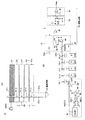
図4(A)に、本発明の実施の形態に関わる接触検出装置の概略的な平面図を示す。この平面図は最表面の保護層を省略し、検出面(保護層の際表面)から装置内部を透視した図である。また、図4(B)に、図4(A)のA−A線に沿った概略断面図を示す。
図4(B)に図解するように、接触検出装置10は、第1基板11と、第2基板12との間に駆動電極DEmが配置されている。第2基板12の駆動電極DEm側と反対の面、すなわち検出面側の面にセンサ線が配置されている。
[Schematic configuration of contact detection device]
FIG. 4A shows a schematic plan view of a contact detection apparatus according to the embodiment of the present invention. In this plan view, the outermost protective layer is omitted, and the inside of the apparatus is seen through from the detection surface (surface when the protective layer is formed). FIG. 4B is a schematic cross-sectional view taken along line AA in FIG.
As illustrated in FIG. 4B, in the
センサ線は、図4(A)に示すようにy方向に細長く2種類の長さをもつ複数の配線から形成されている。以下、比較的長いセンサ線を“ロングセンサ線LSL”と呼び、比較的短いセンサ線を“ショートセンサ線SSL”と呼ぶ。本例では、ロングセンサ線LSLi(i=1,2,3,…,n)とショートセンサ線SSLi(i=1,2,3,…,n)がx方向で交互に配置されている。詳細は後述するが、隣接する長さが異なるセンサ線、すなわちロングセンサ線LSLiとショートセンサ線SSLiを1対として、対ごとにセンサ線出力を演算処理する。また、本例では、ロングセンサ線LSLiはショートセンサ線SSLiの2倍の長さを有する。
以下、n本のロングセンサ線LSLiとn本のショートセンサ線SSLiを総称して“2n本のセンサ線SL”と呼ぶ。
As shown in FIG. 4A, the sensor line is formed of a plurality of wirings that are elongated in the y direction and have two types of lengths. Hereinafter, a relatively long sensor line is referred to as a “long sensor line LSL”, and a relatively short sensor line is referred to as a “short sensor line SSL”. In this example, long sensor lines LSLi (i = 1, 2, 3,..., N) and short sensor lines SSLi (i = 1, 2, 3,..., N) are alternately arranged in the x direction. Although details will be described later, sensor line outputs are calculated for each pair, with adjacent sensor lines having different lengths, that is, a long sensor line LSLi and a short sensor line SSLi as a pair. In this example, the long sensor line LSLi is twice as long as the short sensor line SSLi.
Hereinafter, the n long sensor lines LSLi and the n short sensor lines SSLi are collectively referred to as “2n sensor lines SL”.
駆動電極は、図4(A)に示すように、x方向に長い帯状に形成され、y方向に同一ピッチでm個配置されている。m個の駆動電極DEj(j=1,2,3,…,m)は、2n本のセンサ線SL(LSL+SSL)と、例えば直交して配置されている。 As shown in FIG. 4A, the drive electrodes are formed in a strip shape that is long in the x direction, and m electrodes are arranged at the same pitch in the y direction. The m drive electrodes DEj (j = 1, 2, 3,..., m) are arranged, for example, orthogonally to 2n sensor lines SL (LSL + SSL).
第1基板11と第2基板12の材質を限定しない。ただし、2n本のセンサ線SLの各々がm個の駆動電極DEmと容量結合している必要がある。そのため当該容量結合を所定の強さとするという観点から、第2基板12の厚さや材質が規定されている。その観点では第2基板12を省略し、絶縁物を2n本のセンサ線SLとm個の駆動電極DEmとの間に介在させてよい。 The material of the first substrate 11 and the second substrate 12 is not limited. However, each of the 2n sensor lines SL needs to be capacitively coupled to the m drive electrodes DEm. Therefore, the thickness and material of the second substrate 12 are specified from the viewpoint of making the capacitive coupling have a predetermined strength. From this viewpoint, the second substrate 12 may be omitted, and an insulator may be interposed between the 2n sensor lines SL and the m drive electrodes DEm.
m個の駆動電極DEjの一方端に接続されて走査駆動部9が配置されている。また、2n本のセンサ線SL(LSL+SSL)の一方端に接続されて接触検出部8が配置されている。
A
走査駆動部9は、駆動電極ごとに交流信号源AS(図1,図2参照)を有し、活性化する交流信号源ASを図4(A)の走査駆動部9のブロック内で矢印により示す方向(走査方向)に順次切り替える回路である。あるいは、走査駆動部9は、1つの交流信号源ASを有し、この1つの交流信号源ASと、m個の駆動電極DE1〜DEmのうち1つの駆動電極DEjとの接続を上記走査方向で順次切り替える回路である。
このように実際に交流信号が与えられる駆動電極を、m個の駆動電極の一方端から他方端に向かって切り替える動作を“走査”と呼ぶ。
なお、接触検出部8の機能および構成は後述する。
The
The operation of switching the drive electrodes to which an AC signal is actually applied in this way from one end of the m drive electrodes toward the other end is called “scanning”.
The function and configuration of the contact detection unit 8 will be described later.
本実施の形態では、駆動電極とセンサ線との直交配置は必須ではなく、各センサ線と各駆動電極との容量結合が、検出面内で均一またはほぼ均一となれば、両者の形状や配置を特に限定する必要がない。
ただし、図4(A)のように検出面の直交する2つの辺の一方の側からセンサ線を引き出して接触検出部8に接続し、上記2つの辺のもう片方の側から駆動電極を引き出して走査駆動部9に接続すると、接触検出部8と走査駆動部9の配置が行いやすい。そのため駆動電極とセンサ線との直交配置は望ましいが、これに限定することが必須というわけではない。
In the present embodiment, the orthogonal arrangement of the drive electrode and the sensor line is not essential, and if the capacitive coupling between each sensor line and each drive electrode is uniform or almost uniform within the detection surface, the shape and arrangement of the two There is no need to specifically limit.
However, as shown in FIG. 4A, the sensor wire is drawn out from one side of the two sides orthogonal to the detection surface and connected to the contact detection unit 8, and the drive electrode is drawn out from the other side of the two sides. By connecting to the
[検出信号の信号成分]
図5(A)に、m個の駆動電極DEjのうち、最初の駆動電極DE1を交流信号源ASが駆動している様子を示す。また、図5(B)に、このとき図4(A)に示すn本のロングセンサ線LSLiの任意の1本にユーザの指が近接しているときのタッチセンサの等価回路図を示す。
図5(A)に示すように駆動電極DE1に交流信号源ASが接続されて、駆動電極DE1が交流駆動されている。このときタッチセンサは、図5(B)のような等価回路で表される。ただし、ここでは容量素子C1_1〜C1_mの各静電容量値を“Cp”、ロングセンサ線LSLiに、容量素子C1_1〜C1_m以外に接続されている容量成分(寄生容量)を“Cc”、交流信号源ASによる交流電圧の実効値を“V1”と表す。このとき接触検出部8(図4(A)参照)で検出される検出信号Vdetは、指が非接触のときは電圧Vs、指が接触のときは電圧Vf(<Vs)となる。図3との関係では、電圧Vsが“初期検出信号Vdet0”に相当し、電圧Vfが“検出信号Vdet1”に相当する。以下、電圧Vs,Vfをセンサ電圧という。
[Signal component of detection signal]
FIG. 5A shows a state where the AC signal source AS is driving the first drive electrode DE1 among the m drive electrodes DEj. FIG. 5B shows an equivalent circuit diagram of the touch sensor when the user's finger is close to any one of the n long sensor lines LSLi shown in FIG. 4A.
As shown in FIG. 5A, the AC signal source AS is connected to the drive electrode DE1, and the drive electrode DE1 is AC driven. At this time, the touch sensor is represented by an equivalent circuit as shown in FIG. However, here, the capacitance values of the capacitive elements C1_1 to C1_m are “Cp”, the capacitive component (parasitic capacitance) connected to the long sensor line LSLi other than the capacitive elements C1_1 to C1_m is “Cc”, and an AC signal. The effective value of the AC voltage from the source AS is represented as “V1”. At this time, the detection signal Vdet detected by the contact detection unit 8 (see FIG. 4A) is a voltage Vs when the finger is not in contact and a voltage Vf (<Vs) when the finger is in contact. In the relationship with FIG. 3, the voltage Vs corresponds to the “initial detection signal Vdet0”, and the voltage Vf corresponds to the “detection signal Vdet1”. Hereinafter, the voltages Vs and Vf are referred to as sensor voltages.
非接触時のセンサ電圧Vsは、図5(C)のような式によって表される。この式から、駆動電極DEの数mが大きいと、その分、各静電容量値Cpは小さくなる。このため図5(C)の式の分母における“mCp”がほぼ一定となる。また、寄生容量Ccの値は駆動電極DEの数mの影響を多少は受けるが、ほぼ一定とみなしてよい。このため図5(C)の式の分子に余り大きな変化がないが、その分子が小さくなる。よって、駆動電極DEの数mが大きくなるにしたがって、センサ電圧Vsの大きさ(非接触時の検出信号の波高値)も小さくなる。一方、センサ電圧Vf(接触時の検出信号の波高値)はセンサ電圧Vsと同様に、ほぼ“mCp”に反比例し、ほぼ“Cp”に比例する値をとる。これは、指の近接により付加された外部容量C2の値が静電容量値Cpより十分小さいからである。
以上より、駆動電極DEの数mが大きいほど検出信号の波高値も大きくなる。
The sensor voltage Vs at the time of non-contact is represented by an equation as shown in FIG. From this equation, when the number m of drive electrodes DE is large, each capacitance value Cp is correspondingly reduced. Therefore, “mCp” in the denominator of the equation of FIG. 5C is substantially constant. Further, the value of the parasitic capacitance Cc is somewhat affected by the number m of the drive electrodes DE, but may be regarded as almost constant. For this reason, the numerator of the formula in FIG. 5C does not change much, but the numerator becomes smaller. Therefore, as the number m of drive electrodes DE increases, the magnitude of the sensor voltage Vs (the peak value of the detection signal at the time of non-contact) also decreases. On the other hand, like the sensor voltage Vs, the sensor voltage Vf (the peak value of the detection signal at the time of contact) is approximately inversely proportional to “mCp” and takes a value approximately proportional to “Cp”. This is because the value of the external capacitance C2 added by the proximity of the finger is sufficiently smaller than the capacitance value Cp.
From the above, the peak value of the detection signal increases as the number m of the drive electrodes DE increases.
これに対し駆動電極DEの数mが小さく、1つの駆動電極DE1の面積が大きいと、検出信号の波高値は大きくなるが、被検出物の大きさを検出する際の分解能(認識可能な最小の被検出物の大きさに対応)が低下する。また、被検出物の位置検出の場合は、その位置検出の精度も上記数mが小さいほど高い。よって、この物体の大きさや位置を検出する精度を上げて高性能化すると、どうしても1つの駆動電極DEの面積を小さくせざるを得ない。しかし、前述したように、駆動電極DEの数mを大きくして電極面積を小さくすると、タッチセンサの検出信号の波高値が低下する。 On the other hand, if the number m of the drive electrodes DE is small and the area of one drive electrode DE1 is large, the peak value of the detection signal increases, but the resolution when detecting the size of the detection object (minimum recognizable minimum). Corresponding to the size of the detected object). In the case of detecting the position of an object to be detected, the position detection accuracy is higher as the number m is smaller. Therefore, if the accuracy of detecting the size and position of this object is increased and the performance is improved, the area of one drive electrode DE must be reduced. However, as described above, if the number m of the drive electrodes DE is increased to reduce the electrode area, the peak value of the detection signal of the touch sensor is lowered.
本例では、1つの駆動電極DEの面積に応じて、駆動電極DEと交差する箇所での静電容量値Cpが変化する。つまり、駆動電極DEの面積(特に幅)が大きいほど、静電容量値Cpも大きくなる。また、静電容量値Cpは、1本のセンサ線SLiの面積(特に幅)が大きいほど、静電容量値Cpも大きくなる。 In this example, the capacitance value Cp at a location intersecting with the drive electrode DE changes according to the area of one drive electrode DE. That is, the capacitance value Cp increases as the area (particularly the width) of the drive electrode DE increases. Further, the capacitance value Cp increases as the area (particularly the width) of one sensor line SLi increases.
ところで、センサ線SLiにノイズがのると、結果として、検出信号Vdet中のノイズ成分に対して信号成分(センサ電圧Vs,Vfの平均的な波高値)が相対的に小さくなる。したがって、検出信号VdetのS/N比が低下してしまう。このS/N比は、駆動電極DEの数mが大きく1つの駆動電極DEの幅が小さいほど低下する。また、信号成分とノイズ成分の大きさ(ノイズ量)が近接するほどノイズ分離技術の適用が難しくなる。とくにノイズ成分が周期的に変動し、その周期が検出信号の周期に近いと、さらにノイズ分離が難しくなる。
よって、タッチセンサの感度(検出する物体の大きさの解像度や位置検出精度)と検出信号VdetのS/N比にはトレードオフの関係があり、ノイズフィルタ等のノイズ分離技術を適用したとしても、両者を共に向上させることは困難である。
By the way, when noise is applied to the sensor line SLi, as a result, the signal component (average peak values of the sensor voltages Vs and Vf) is relatively small with respect to the noise component in the detection signal Vdet. Therefore, the S / N ratio of the detection signal Vdet is lowered. The S / N ratio decreases as the number m of drive electrodes DE is large and the width of one drive electrode DE is small. Also, the closer the magnitude of the signal component and the noise component (noise amount), the more difficult it is to apply the noise separation technique. In particular, when noise components fluctuate periodically and the period is close to the period of the detection signal, noise separation becomes more difficult.
Therefore, there is a trade-off relationship between the sensitivity of the touch sensor (the resolution of the size of the object to be detected and the position detection accuracy) and the S / N ratio of the detection signal Vdet. Even if a noise separation technique such as a noise filter is applied. It is difficult to improve both.
図5は、最初の駆動電極DEとロングセンサ線LSLiとの交差部分を駆動した場合であるが、ここで、ショートセンサ線SSLiの駆動にも言及する。
ロングセンサ線LSLi(図4(A)参照)はm個の駆動電極DE全てと交差しているため、このとき図5(C)に示す式の分母が“mCp+Cc”である。これに対し、ショートセンサ線SSLi(図4(A)参照)において、駆動電極DEとの交差箇所がロングセンサ線LSLiの約半数である。そのため、図5(C)に示す式の分母が“mCp/2+Cc”となる。ここで総結合容量、すなわち“mCp”や“mCp/2”に対し寄生容量Ccが十分小さいとする。この仮定のもとでは、ショートセンサ線SSLiから出力される検出信号Vdetの信号成分(センサ電圧Vs,Vfの平均的な波高値)がロングセンサ線LSLiの場合の約2倍となる。
FIG. 5 shows a case where the intersection of the first drive electrode DE and the long sensor line LSLi is driven. Here, the driving of the short sensor line SSLi is also referred to.
Since the long sensor line LSLi (see FIG. 4A) intersects with all the m drive electrodes DE, the denominator of the equation shown in FIG. 5C is “mCp + Cc”. On the other hand, in the short sensor line SSLi (see FIG. 4A), the intersection with the drive electrode DE is about half of the long sensor line LSLi. Therefore, the denominator of the equation shown in FIG. 5C is “mCp / 2 + Cc”. Here, it is assumed that the parasitic capacitance Cc is sufficiently smaller than the total coupling capacitance, that is, “mCp” or “mCp / 2”. Under this assumption, the signal component of the detection signal Vdet output from the short sensor line SSLi (average peak value of the sensor voltages Vs and Vf) is about twice that of the long sensor line LSLi.
なお、検出信号Vdetの信号成分がショートセンサ線でロングセンサ線の2倍となることは、各センサ線の寄生容量Ccが総結合容量(mCp,mCp/2)より十分小さい仮定(以下、第1仮定)のもとでの結論である。
これに対し、各センサ線の寄生容量Ccが総結合容量(mCp,mCp/2)より十分大きいと仮定する(以下、第2仮定)。この第2仮定のもとでは、図5(C)の式における分母で寄生容量Ccが支配的となるが、寄生容量Ccは配線容量に比例し配線容量が小さいほど小さくなる。つまり、ショートセンサ線の寄生容量Ccはロングセンサ線の寄生容量Ccからほぼ半減する。よって、検出信号Vdetの信号成分がショートセンサ線でロングセンサ線の2倍となるという結論は、第2仮定でも変わらない。
一方、第1仮定と第2仮定の中間、つまり、図5(C)の式における分母で総結合容量(mCp,mCp/2)と寄生容量Ccのどちらも無視できない値を有する場合を考える(第3仮定)。この場合も、図5(C)の式における分母が、ショートセンサ線の場合がロングセンサ線の場合の半分であることは容易に類推でき、結論は変わらない。
Note that the signal component of the detection signal Vdet is twice that of the long sensor line in the short sensor line, assuming that the parasitic capacitance Cc of each sensor line is sufficiently smaller than the total coupling capacity (mCp, mCp / 2) (hereinafter referred to as the first). This is a conclusion under (1 assumption).
On the other hand, it is assumed that the parasitic capacitance Cc of each sensor line is sufficiently larger than the total coupling capacitance (mCp, mCp / 2) (hereinafter, second assumption). Under this second assumption, the parasitic capacitance Cc is dominant in the denominator in the equation of FIG. 5C, but the parasitic capacitance Cc is proportional to the wiring capacitance and decreases as the wiring capacitance decreases. That is, the parasitic capacitance Cc of the short sensor line is almost halved from the parasitic capacitance Cc of the long sensor line. Therefore, the conclusion that the signal component of the detection signal Vdet is twice that of the long sensor line in the short sensor line does not change even in the second assumption.
On the other hand, a case where the total coupling capacitance (mCp, mCp / 2) and the parasitic capacitance Cc have values that cannot be ignored in the denominator in the equation of FIG. Third assumption). Also in this case, it can be easily inferred that the denominator in the equation of FIG. 5C is half of the case of the short sensor line and that of the long sensor line, and the conclusion remains unchanged.
以上より、ショートセンサ線の長さをロングセンサ線の長さの(1/2)倍に設定していると、ショート側の信号成分がロング側の2倍となる。その前提は、ロングセンサ線とショートセンサ線を幅が同じで材質や厚さも同じ配線層から形成していることである。
一般に配線層は、配線幅、厚さおよび材質が同じだと、長さに比例した配線容量をもつ。したがって、このことを一般化すると、「幅、厚さおよび材質が同じロングセンサ線とショートセンサ線は、その長さの比が配線容量比Kcとほぼ一致し、配線容量比Kcにほぼ反比例して検出信号の信号成分の大きさ(波高値)が規定される」といえる。
なお、本発明で“配線容量”と言うとき、配線層自身の容量に、寄生容量や他の導電部位との結合容量を付加した容量を意味する。
From the above, when the length of the short sensor line is set to (1/2) times the length of the long sensor line, the signal component on the short side is twice that on the long side. The premise is that the long sensor wire and the short sensor wire are formed of the same wiring layer and the same material and thickness.
In general, a wiring layer has a wiring capacity proportional to the length if the wiring width, thickness and material are the same. Therefore, this can be generalized as follows: “Long sensor wires and short sensor wires having the same width, thickness, and material have a length ratio that is substantially the same as the wiring capacitance ratio Kc and is almost inversely proportional to the wiring capacitance ratio Kc. Thus, it can be said that the magnitude (crest value) of the signal component of the detection signal is defined.
In the present invention, the “wiring capacitance” means a capacitance obtained by adding a parasitic capacitance or a coupling capacitance with another conductive portion to the capacitance of the wiring layer itself.
<2.第1変形例>
ここで配線容量比Kcを変化させる他の態様(変形例)を説明する。
第1変形例では、2つのセンサ線の長さ、厚さ、材質が同じで、幅が異なる。
例えば、第1センサ線に対し2倍の幅を有する第2センサ線を考える。その場合、第2センサ線の第1センサ線に対する配線容量比Kcが約2であり、図5(C)に示す式の分母も第2センサ線側で第1センサ線側の約2倍となる。この場合、m個の駆動電極DEjの各電極幅が一定とすると、静電容量値Cpが第2センサ線で第1センサ線の約2倍となる。よって、変形例1では、検出信号の信号成分(波高値)が第1および第2センサ線でほぼ同じになる。
<2. First Modification>
Here, another mode (modification) for changing the wiring capacitance ratio Kc will be described.
In the first modification, the length, thickness, and material of the two sensor lines are the same, but the widths are different.
For example, consider a second sensor line having a width twice that of the first sensor line. In that case, the wiring capacitance ratio Kc of the second sensor line to the first sensor line is about 2, and the denominator of the equation shown in FIG. 5C is also about twice the first sensor line side on the second sensor line side. Become. In this case, if the electrode widths of the m drive electrodes DEj are constant, the capacitance value Cp is about twice that of the first sensor line in the second sensor line. Therefore, in the first modification, the signal component (crest value) of the detection signal is substantially the same in the first and second sensor lines.
<3.第2変形例>
第2変形例では、2つのセンサ線の厚さと材質が同じで、長さと幅が異なる。
例えば、図4と同じようにショートセンサ線がロングセンサ線の半分、すなわち(1/2)倍の長さを有し、ショートセンサ線の幅がロングセンサ線の幅の(1/2)倍であるとする。この場合、図5(C)の分母がショートセンサ線側でロングセンサ線側の約(1/4)倍となる(配線容量比Kcが4または1/4)。また、静電容量値Cpはショートセンサ線側でロングセンサ線側の約(1/2)倍となる。したがって、第2変形例においては、ショートセンサ線から出力される検出信号の信号成分(波高値)は、ロングセンサ線から出力される検出信号の信号成分(波高値)の約2倍となる。
<3. Second Modification>
In the second modification, the thickness and material of the two sensor wires are the same, but the length and width are different.
For example, as in FIG. 4, the short sensor line is half the long sensor line, that is, (1/2) times as long, and the width of the short sensor line is (1/2) times the width of the long sensor line. Suppose that In this case, the denominator in FIG. 5C is about (1/4) times that of the long sensor line side on the short sensor line side (wiring capacitance ratio Kc is 4 or 1/4). Further, the capacitance value Cp is about (1/2) times that of the long sensor line on the short sensor line side. Therefore, in the second modification, the signal component (crest value) of the detection signal output from the short sensor line is about twice the signal component (crest value) of the detection signal output from the long sensor line.
<4.第3変形例>
第3変形例では、第2変形例と同様に、2つのセンサ線の厚さと材質が同じで、長さと幅が異なる。
ただし、図4と同じようにショートセンサ線がロングセンサ線の(1/2)倍の長さを有するが、ショートセンサ線の幅がロングセンサ線の幅の2倍であるとする。この場合、図5(C)の分母がショートセンサ線側とロングセンサ線側で変わらない(配線容量比Kcが1)。また、静電容量値Cpがショートセンサ線側でロングセンサ側の約2倍となる。したがって、第3変形例においては、ショートセンサ線から出力される検出信号の信号成分(波高値)は、ロングセンサ線から出力される検出信号の信号成分(波高値)の約2倍となる。
<4. Third Modification>
In the third modification, as in the second modification, the thickness and material of the two sensor lines are the same, and the length and width are different.
However, it is assumed that the short sensor line is (1/2) times as long as the long sensor line as in FIG. 4, but the width of the short sensor line is twice the width of the long sensor line. In this case, the denominator in FIG. 5C does not change between the short sensor line side and the long sensor line side (wiring capacitance ratio Kc is 1). Further, the capacitance value Cp is about twice as long on the short sensor line side as that on the long sensor side. Therefore, in the third modification, the signal component (peak value) of the detection signal output from the short sensor line is approximately twice the signal component (peak value) of the detection signal output from the long sensor line.
図4の場合、ならびに、第1〜第3変形例では、一方のセンサ線に対し他方のセンサ線の長さのみを変え、幅のみを変え、または、長さと幅の両方を変え、その変化倍率を2とした。しかし、この変化倍率を3としてもよいし、それ以外の自然数にしてもよい。これにより、一方のセンサ線の検出信号の信号成分に対して他方のセンサ線の信号成分を等倍、2倍、3倍、…と任意の自然数倍に変化させることが可能となる。
このことは、逆の見方をすると、他方のセンサ線の検出信号の信号成分に対して一方のセンサ線の信号成分を等倍、(1/2)倍、(1/3)倍、…と任意の自然数の逆数倍に変化させることを意味する。
In the case of FIG. 4 and the first to third modifications, only the length of one sensor line is changed, only the width is changed, or both the length and width are changed, and the change is made. The magnification was 2. However, this change magnification may be 3 or any other natural number. This makes it possible to change the signal component of the other sensor line to the same natural number, two times, three times,... Any natural number times with respect to the signal component of the detection signal of one sensor line.
In other words, the signal component of one sensor line is equal to, (1/2) times, (1/3) times,... The signal component of the detection signal of the other sensor line. It means changing to an inverse multiple of any natural number.
また、図4の場合、ならびに、第1〜第3変形例では、長さと幅の少なくとも一方を変えたが、配線容量比Kcを変化させるパラメータは、長さ、幅のほかに、配線層の材質、厚さも関係してくる。よって、センサ線を形成するときの配線層の材質、厚さを単独で、あるいは、他のパラメータと組み合わせることで配線容量比Kcを2つのセンサ線間で変えてもよい。 In the case of FIG. 4 and in the first to third modifications, at least one of the length and the width is changed, but the parameter for changing the wiring capacitance ratio Kc is not only the length and the width but also the wiring layer. Material and thickness are also related. Therefore, the wiring capacitance ratio Kc may be changed between the two sensor lines by combining the material and thickness of the wiring layer when forming the sensor lines alone or in combination with other parameters.
[ノイズ成分]
ノイズ成分は、想定するノイズ源によって、そのセンサ線への重畳のしかたが異なる。
接触検出装置は、それ自身で薄型化、高機能化を行い、さらには他の電子機器(例えば後述する実施の形態のように表示装置)へ搭載されることがある。そのため、接触検出装置のセンサ線より下層側に電位変動する他の配線が配置され、薄型化にともない、その配線とセンサ線との距離も縮まる傾向にある。
[Noise component]
The method of superimposing the noise component on the sensor line differs depending on the assumed noise source.
The contact detection device itself is thinned and highly functional, and may be mounted on another electronic device (for example, a display device as in an embodiment described later). For this reason, another wiring that varies in potential is arranged on the lower layer side of the sensor line of the contact detection device, and the distance between the wiring and the sensor line tends to be shortened as the thickness is reduced.
ノイズ源として電位変動する配線が、仮にセンサ線と平行に配置される場合、厚さや材質も関係するが、主に長さと幅を主要パラメータとする容量結合の強さでノイズ成分の大きさ(ノイズ量)が規定される。
ここで、ノイズは寄生容量Ccを介してセンサ線に重畳されるため、寄生容量Ccが大きいほどノイズ量も大きくなる関係がある。但し、既に述べたように寄生容量Ccは配線容量に比例し、この意味では配線容量が大きいほどノイズ量も大きくなるようにも思われる。しかし、その一方で、センサ線の配線容量が大きいと、ノイズによってセンサ線の電位変化が起きにくい。このため、配線容量比Kcが変化してもノイズ量は殆んど変化しない。
If the wiring that fluctuates in potential as a noise source is placed in parallel with the sensor line, the thickness and material are also related, but the magnitude of the noise component (mainly the strength of capacitive coupling with the length and width as the main parameters ( Noise amount).
Here, since noise is superimposed on the sensor line via the parasitic capacitance Cc, there is a relationship in which the amount of noise increases as the parasitic capacitance Cc increases. However, as already described, the parasitic capacitance Cc is proportional to the wiring capacitance. In this sense, it seems that the larger the wiring capacitance, the larger the noise amount. However, when the wiring capacity of the sensor line is large, the potential change of the sensor line is unlikely to occur due to noise. For this reason, the amount of noise hardly changes even if the wiring capacitance ratio Kc changes.
例えば、センサ線の幅が同じで長さが半減する場合(配線容量比Kc=2または1/2)、長さが半減することにともなって配線容量(静電容量値Cp)が半減し、このとき寄生容量Ccも半減する。このため、センサ線の長さが変化してもノイズ量は殆んど変化しない。
また、センサ線の長さが同じで幅が半減する場合(配線容量比Kc=2または1/2)、幅が半減することにともなって配線容量(静電容量値Cp)が半減し、このとき寄生容量Ccも半減する。このため、センサ線の幅が変化してもノイズ量は殆んど変化しない。
For example, when the sensor line width is the same and the length is halved (wiring capacitance ratio Kc = 2 or 1/2), the wiring capacitance (capacitance value Cp) is halved as the length is halved, At this time, the parasitic capacitance Cc is also halved. For this reason, even if the length of the sensor line changes, the amount of noise hardly changes.
Further, when the sensor wire length is the same and the width is halved (wiring capacitance ratio Kc = 2 or 1/2), the wiring capacitance (capacitance value Cp) is halved as the width is halved. Sometimes the parasitic capacitance Cc is also halved. For this reason, the amount of noise hardly changes even if the width of the sensor line changes.
一方、ノイズ源の配線が、仮にセンサ線の幅方向を横切る場合、厚さや材質も関係するが、主に幅を主要パラメータとする容量結合の強さでノイズ成分の大きさが規定される。この場合もノイズは寄生容量Ccを介してセンサ線に重畳され、既に述べたように寄生容量Ccは配線容量に比例し配線容量が大きいほど大きくなるようにも思われる。しかし、幅が大きくなる分、配線容量も大きくなるため、ノイズによってセンサ線の電位変化が起きにくく、この場合も配線容量比Kcが変化してもノイズ量は殆んど変化しない。例えば、図4に示す同じ幅のロングセンサ線LSLiとショートセンサ線SSLiを横切る配線がノイズ源となる場合、この2つのセンサ線には同じ程度のノイズ成分が重畳される。 On the other hand, if the noise source wiring crosses the width direction of the sensor line, the thickness and the material are related, but the magnitude of the noise component is mainly defined by the strength of capacitive coupling whose width is the main parameter. In this case as well, noise is superimposed on the sensor line via the parasitic capacitance Cc, and as described above, the parasitic capacitance Cc is proportional to the wiring capacitance and seems to increase as the wiring capacitance increases. However, since the wiring capacity increases as the width increases, the potential of the sensor line does not easily change due to noise. In this case, the amount of noise hardly changes even if the wiring capacity ratio Kc changes. For example, when a wiring crossing the long sensor line LSLi and the short sensor line SSLi having the same width shown in FIG. 4 is a noise source, the same noise component is superimposed on the two sensor lines.
ノイズ源は外部から飛来する電磁波となる場合もある。このときセンサ線がアンテナとしてノイズを拾う。
この場合、センサ線の厚さや材質も関係するが、主に長さ、あるいは、長さと幅を主要パラメータとする容量結合の強さでノイズ成分の大きさが規定される。この場合、センサ線に重畳されるノイズは、寄生容量Ccを介したものでないため、ノイズ成分は配線容量と比例する傾向がある。よって、この場合の飛来ノイズ量は、配線容量比Kcに応じたものとなる。
The noise source may be electromagnetic waves flying from the outside. At this time, the sensor line picks up noise as an antenna.
In this case, although the thickness and material of the sensor line are also related, the size of the noise component is mainly defined by the length or the strength of capacitive coupling having the length and width as main parameters. In this case, since the noise superimposed on the sensor line is not via the parasitic capacitance Cc, the noise component tends to be proportional to the wiring capacitance. Therefore, the amount of incoming noise in this case depends on the wiring capacitance ratio Kc.
以上から、ノイズ源によっては配線容量比Kcと相関する場合(飛来ノイズの場合)もあるが、センサ線に電位変化する配線が近接する場合、この配線からの誘導ノイズが支配的であり、飛来ノイズの全体のノイズ量に占める割合は無視できるほど小さいと仮定できる。よって、配線容量比Kcを用いた演算処理によりノイズ成分を除去する際に、ノイズ量は配線容量比Kcによらずほぼ一定と仮定してもノイズ除去演算の精度を低下させない。
なお、詳細な演算手法は示さないが、飛来ノイズ等、ノイズ量が配線容量比Kcと相関するノイズ源が無視できない場合は、ノイズ量を一定としないノイズ除去演算も可能である。
From the above, some noise sources may correlate with the wiring capacitance ratio Kc (in the case of flying noise), but when a wiring whose potential changes is close to the sensor line, the induced noise from this wiring is dominant, and the flying noise It can be assumed that the ratio of noise to the total amount of noise is negligibly small. Therefore, when the noise component is removed by calculation processing using the wiring capacitance ratio Kc, the accuracy of the noise removal calculation does not decrease even if the noise amount is assumed to be substantially constant regardless of the wiring capacitance ratio Kc.
Although a detailed calculation method is not shown, if noise sources whose noise amount correlates with the wiring capacitance ratio Kc cannot be ignored, such as incoming noise, noise removal calculation without making the noise amount constant is possible.
[ノイズ除去演算]
つぎに、センサ線の長さに応じて検出信号の信号成分が異なる場合を主な例として、そのとき得られる配線容量比Kcを利用したノイズ除去演算について説明する。
[Noise reduction calculation]
Next, the noise removal calculation using the wiring capacitance ratio Kc obtained at that time will be described mainly using the case where the signal component of the detection signal varies depending on the length of the sensor line.
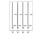
図6(A)は、ロングセンサ出力とショートセンサ出力の波形を示すための図である。
図6(A)において“Long Sensor(L)”と表記する波形図はロングセンサ線LSLiの出力波形を示す。また、“Sort Sensor(S)”と表記する波形図はショートセンサ線SSLiの出力波形を示す。これらの出力波形で、横軸は時間t(単位[μs])の推移を、縦軸は基準電位(例えば0[V])中心としたセンサ線出力電位変動を表している。横軸は時間ゼロから時間16.67[msec]の範囲をとる。駆動電極を交流駆動した結果、センサ線出力も交流変化しているが、図6(A)の横軸に対してその電位変動周期が極めて小さいため交流波形の山が1本の線として見えている。
図6(A)でボーダ(Border)と表記されている領域は、図4(A)や図5(A)において交流信号源ASが接続または活性化している駆動電極DEに対応する検出面からみた領域を指す。
FIG. 6A is a diagram for illustrating waveforms of the long sensor output and the short sensor output.
In FIG. 6A, a waveform diagram denoted as “Long Sensor (L)” indicates an output waveform of the long sensor line LSLi. A waveform diagram denoted as “Sort Sensor (S)” shows an output waveform of the short sensor line SSLi. In these output waveforms, the horizontal axis represents the transition of time t (unit [μs]), and the vertical axis represents the sensor line output potential fluctuation centered on the reference potential (for example, 0 [V]). The horizontal axis ranges from time zero to time 16.67 [msec]. As a result of AC driving of the drive electrode, the sensor line output also changes in AC. However, since the potential fluctuation period is extremely small with respect to the horizontal axis in FIG. 6A, the peak of the AC waveform appears as one line. Yes.
The area labeled “Border” in FIG. 6A is from the detection surface corresponding to the drive electrode DE to which the AC signal source AS is connected or activated in FIG. 4A or 5A. Refers to the observed area.
図6(B)は、“Long Sensor(L)”の波形図に対応するロングセンサ線出力の模式的説明図である。図6(C)は、“Sort Sensor(S)”の波形図に対応するショートセンサ線出力の模式的説明図である。
ここで、ボーダのy方向の幅が移動ピッチより大きく設定されている。これは、図5(A)に示す駆動電極DEの分割数を多くして、その代わり、交流信号源ASによって一度に駆動する駆動電極DEの数を複数にすることで実施できる。つまり、一度に駆動する駆動電極DEを、例えば数個〜数十個に設定し、走査時のシフトのピッチを例えば駆動電極1つ分とする。なお、この駆動電極の複数駆動と狭ピッチ走査は、本実施の形態では必須ではないが、図6では、この駆動走査方法を採用している。
FIG. 6B is a schematic explanatory diagram of a long sensor line output corresponding to the waveform diagram of “Long Sensor (L)”. FIG. 6C is a schematic explanatory diagram of the short sensor line output corresponding to the waveform diagram of “Sort Sensor (S)”.
Here, the width of the border in the y direction is set larger than the movement pitch. This can be implemented by increasing the number of divisions of the drive electrode DE shown in FIG. 5A and, instead, increasing the number of drive electrodes DE driven at a time by the AC signal source AS. That is, the number of drive electrodes DE driven at a time is set to several to several tens, for example, and the shift pitch during scanning is set to one drive electrode, for example. Note that the plurality of driving electrodes and narrow pitch scanning are not essential in this embodiment, but this driving scanning method is adopted in FIG.
図6(B)と図6(C)に記載した数字“0”と“800”は、y方向走査のシフトピッチ数を表している。その真中の“400”を境に“0〜400”がA領域に相当し、“400〜800”がB領域に相当する。 The numbers “0” and “800” shown in FIGS. 6B and 6C represent the number of shift pitches in the y-direction scanning. In the middle of “400”, “0 to 400” corresponds to the A region, and “400 to 800” corresponds to the B region.
ボーダ(Border)が図6(A)の状態から矢印の向きに移動する。
ロングセンサ線LSLiのみがボーダ(border)と交差するA領域の走査では、ロングセンサ線LSLiからは“Long Sensor(L)”と表記する波形の検出信号Vdetが出力される。A領域中の走査において、ロングセンサ線出力は図6(B)に示すように、1倍の信号成分Sと1倍のノイズ成分が重畳していると定義する。このとき、ショートセンサ線出力は図6(C)に示すように、まだボーダと交差する前の段階であるため、ノイズ成分のみが出現する。
ここで[ノイズ成分]の項で前述したように、ノイズ成分は配線容量比Kcによらず一定であると仮定することができるため、ショートセンサ線出力のノイズ成分も1倍(=N)で表記される。
The border moves from the state of FIG. 6A in the direction of the arrow.
In the scanning of the area A where only the long sensor line LSLi intersects the border, a detection signal Vdet having a waveform expressed as “Long Sensor (L)” is output from the long sensor line LSLi. In scanning in the area A, the long sensor line output is defined as superimposing a signal component S of 1 time and a noise component of 1 time as shown in FIG. 6B. At this time, as shown in FIG. 6C, the short sensor line output is still in a stage before crossing the border, so that only a noise component appears.
Here, as described above in the section of [Noise component], it can be assumed that the noise component is constant regardless of the wiring capacitance ratio Kc, so the noise component of the short sensor line output is also 1 time (= N). It is written.
図6(C)には、信号成分Sを求めるための演算式(Kc=2の場合)と、配線容量比Kcを用いた一般化の式を例示している。このように、長さが異なる2本のセンサ線の出力から、配線容量比Kcを用いることによって、ノイズ成分が除去された信号成分Sを演算により求めることができる。 FIG. 6C illustrates an arithmetic expression for obtaining the signal component S (in the case of Kc = 2) and a generalized expression using the wiring capacitance ratio Kc. Thus, the signal component S from which the noise component has been removed can be obtained by calculation from the outputs of two sensor lines having different lengths by using the wiring capacitance ratio Kc.
図7(B)に、図6(C)に示す演算式による演算を3つの位置の走査時に得られた検出信号から演算した結果を表にまとめて示す。また、図7(A)に位置<1>〜<3>とセンサ線との関係を示す。
演算回路には、領域Bにボーダがあるときの位置<1>、領域Aと領域Bの境界にボーダ幅中心があるときの位置<2>、領域Aにボーダがあるときの位置<3>の順で時系列に検出信号が入力される。演算回路は、ロングセンサ線LSLiの出力と、ショートセンサ線SSLiの出力を入力し、その差分(Delta)と配線容量比Kcを用いた演算により信号成分Sを求める。
FIG. 7B shows a table summarizing results obtained by calculating from the detection signals obtained at the time of scanning three positions by the calculation using the calculation formula shown in FIG. 6C. FIG. 7A shows the relationship between the positions <1> to <3> and the sensor lines.
The arithmetic circuit includes a position <1> when the border is in the region B, a position <2> when the border width center is at the boundary between the region A and the region B, and a position <3> when the border is in the region A. In this order, detection signals are input in time series. The arithmetic circuit receives the output of the long sensor line LSLi and the output of the short sensor line SSLi, and obtains the signal component S by calculation using the difference (Delta) and the wiring capacitance ratio Kc.
図7(B)に示すように、演算回路は、位置<3>に対応する検出時間帯では、単に差分(Delta)を演算し、位置<1>に対応する検出時間帯では、差分(Delta)と配線容量比Kcを用いた演算式「(Delta)/(Kc−1)」を用いた演算を実行する。また、位置<2>に対応する検出時間帯では、例えばKc=2の場合に差分(Delta)=0となり演算が成り立たないので、この中間の検出時間帯では演算を行わない。
なお、検出時間帯の判断は検出走査、すなわち図6(A)のボーダのシフト動作と同期したクロック信号を入力して、クロック信号をもとに時間帯の判断を行う。
As shown in FIG. 7B, the arithmetic circuit simply calculates the difference (Delta) in the detection time zone corresponding to the position <3>, and the difference (Delta) in the detection time zone corresponding to the position <1>. ) And an arithmetic expression “(Delta) / (Kc−1)” using the wiring capacitance ratio Kc. Further, in the detection time zone corresponding to the position <2>, for example, when Kc = 2, the difference (Delta) = 0 and the calculation does not hold, so the calculation is not performed in this intermediate detection time zone.
The detection time zone is determined by inputting a clock signal synchronized with the detection scanning, that is, the shift operation of the border shown in FIG. 6A, and determining the time zone based on the clock signal.
他の方法として、Kc=2に限れば差分(Delta)がそのまま信号成分Sとなるので、位置<1>または位置<3>に対応した検出タイミングで演算回路が検出信号Vdetをサンプリングして信号成分Sを求めてもよい。
なお、配線容量比Kcが3以上の場合は、位置<3>に対応した検出タイミングで演算回路が検出信号Vdetをサンプリングして信号成分Sを求めてよい。一方、位置<1>に対応した検出タイミングの場合、差分(Delta)の一般式は「(Kc−1) (Delta)」となるので演算回路は、「(Delta)/(Kc−1)」を演算することにより信号成分Sを求めることができる。
As another method, since the difference (Delta) becomes the signal component S as it is if Kc = 2, the arithmetic circuit samples the detection signal Vdet at the detection timing corresponding to the position <1> or the position <3> Component S may be determined.
When the wiring capacitance ratio Kc is 3 or more, the arithmetic circuit may sample the detection signal Vdet at the detection timing corresponding to the position <3> to obtain the signal component S. On the other hand, in the case of the detection timing corresponding to the position <1>, the general expression of the difference (Delta) is “(Kc−1) (Delta)”, so that the arithmetic circuit is “(Delta) / (Kc−1)”. The signal component S can be obtained by calculating.
このようにして求めた演算回路からの出力は、不図示の回路(当該位置検出装置の内部回路か外部の回路かを問わない)で被検出物の有無や位置を判定する処理に供せられる。 The output from the arithmetic circuit obtained in this way is used for processing for determining the presence and position of an object to be detected by a circuit (not shown) (whether it is an internal circuit or an external circuit of the position detection device). .
なお、長さが同じで幅が異なる2つのセンサ線の演算では、容量式の場合、前述した<第1変形例>で述べたように検出信号の信号成分が幅が異なっても同じ場合があり、また、前述した[ノイズ成分]で述べたようにノイズ成分も同じ場合がある。その場合、幅が異なっても信号成分とノイズ成分の比が変わらない。そのため、上記長さが異なる場合と同様な配線容量比Kcを用いた演算ができない。
但し、容量式以外の場合、さらに容量式でも、例えば飛来ノイズのように配線容量比Kcに応じてノイズ成分が変化する場合もあり得る。その場合、詳しい説明は省略するが、上記の長さが異なる場合と同様な考えで、信号成分とノイズ成分の比の違いを利用して信号成分Sを求める演算が可能である。
In the calculation of two sensor lines having the same length but different widths, in the case of the capacitance type, as described in the above <First modification>, the same case may be obtained even if the signal components of the detection signals have different widths. In addition, as described in the above [Noise component], the noise component may be the same. In that case, the ratio of the signal component to the noise component does not change even if the width is different. Therefore, the calculation using the wiring capacitance ratio Kc similar to the case where the lengths are different cannot be performed.
However, in cases other than the capacitance type, even in the capacitance type, the noise component may change according to the wiring capacitance ratio Kc, for example, flying noise. In this case, although a detailed description is omitted, the signal component S can be calculated using the difference in the ratio between the signal component and the noise component based on the same idea as when the lengths are different.
[交流信号源と演算回路の構成例]
図8(B)は、接触検出部8内の演算回路8Aと交流信号源ASの一構成例を示す回路図である。図8(A)は、駆動電極の駆動位置を示す図である。
図8(A)において、斜線により示す駆動電極DE1が交流信号源ASに接続されて活性化しており、それ以外の非選択の駆動電極DE2〜DEmがGND電位で保持されている。駆動電極が選択されて活性化された状態をオン状態(ON)、非選択の状態をオフ状態ともいう。図8(B)は、これらの駆動電極群に交差する、あるロングセンサ線LSLi(i=1〜n)に接続された接触検出部8内の1つの演算回路8Aと、交流信号源ASの回路図を示している。演算回路8Aは、ロングセンサ線LSLiと対で近接配置されたショートセンサ線SSLi(i=1〜n)も入力し、LSL出力とSSL出力間で所定の演算を行う回路である。
[Configuration example of AC signal source and arithmetic circuit]
FIG. 8B is a circuit diagram showing a configuration example of the
In FIG. 8A, the drive electrode DE1 indicated by hatching is connected to the AC signal source AS and activated, and the other non-selected drive electrodes DE2 to DEm are held at the GND potential. A state in which the drive electrode is selected and activated is also referred to as an on state (ON), and a non-selected state is also referred to as an off state. FIG. 8B shows an
ロングセンサ線LSLiと各駆動電極DEj(j=1〜m)との各交差部分に、(静電)容量素子C1_1〜C1_mが形成される。 (Electrostatic) capacitance elements C1_1 to C1_m are formed at each intersection of the long sensor line LSLi and each drive electrode DEj (j = 1 to m).
図8(B)に図解する交流信号源ASは、制御部91と、2つのスイッチSW(+),SW(−)と、ラッチ回路92と、バッファ回路(波形整形部)93と、出力スイッチSWとを有する。制御部91は、プラス電圧V(+)とマイナス電圧V(−)を各々がスイッチする2つのスイッチSW(+),SW(−)と、出力スイッチSWとを制御する回路である。制御部91は、交流信号源AS内に設けなくとも、外部のCPU等で代用できる。
The AC signal source AS illustrated in FIG. 8B includes a
スイッチSW(+)はプラス電圧V(+)とラッチ回路92の入力との間に接続され、スイッチSW(−)はマイナス電圧V(−)とラッチ回路92の入力との間に接続されている。ラッチ回路92の出力はバッファ回路93を介して、出力スイッチSWのオン側ノードに接続されている。バッファ回路93はプラス電圧V(+)とマイナス電圧V(−)に、入力電位を電位補償して出力する回路である。ここで出力スイッチSWは、制御部91により制御されて、当該交流信号源ASをオン(選択状態あるいは活性状態)とするか、非活性のGND接続とするかを制御する。この制御部91の機能は他の交流信号源ASとの制御と同期させる関係上、通常は、たとえば活性化する交流信号源ASのグループをシフトして選択する信号を、シフトレジスタ等で順送りする等の構成によって実施される。
The switch SW (+) is connected between the positive voltage V (+) and the input of the
(静電)容量素子C1_1〜C1_mが接続されたロングセンサ線LSLiに、演算回路8Aが接続されている。ショートセンサ線SSLiにも演算回路8Aが接続されているが、ショートセンサ線SSLiに接続される(静電)容量素子はロングセンサ線LSLiの半分の数である。
図8に図解する演算回路8Aは、差分演算器(例えばOPアンプ)80、2つの係数乗算器(例えばOPアンプ回路)81、整流回路82および出力回路83から構成される。
The
The
係数乗算器81は、例えば図8(B)に示すように、OPアンプ84、抵抗R1とR2、および、容量C3を有して構成できる。係数乗算器81は、入力するLSL出力<L>またはSSL出力<S>に所定の係数、例えば図7(B)に示す係数(配線容量比Kc=1/3 または2/3)を乗算する乗算器として機能する。係数乗算器81は、抵抗のほかに容量C3を有することから高周波ノイズの除去機能も有する。
係数乗算器81が入力に対して乗算する係数は、(1+r2/r1)で表すことができる(r1:抵抗R1の値、r2:抵抗R2の値)。LSL出力<L>を入力する係数乗算器81は、(1+r2/r1)=1/3となるように抵抗R1,R2の値が決められている。SSL出力<S>を入力する係数乗算器81は、(1+r2/r1)=2/3となるように抵抗R1,R2の値が決められている。
For example, as shown in FIG. 8B, the
The coefficient multiplied by the input by the
図8(B)においてOPアンプ84の非反転入力「+」にロングセンサ線LSLiが接続され、ここから検出信号Vdet(LSL出力<L>)が入力される。ロングセンサ線LSLiは、その電位のDCレベルを電気的にリセットするためのリセットスイッチRSWを介して接地電位に接続されている。OPアンプ84の出力と反転入力「−」との間に抵抗R2と容量C3が並列接続され、OPアンプ84の反転入力「−」と接地電位との間に抵抗R1が接続されている。
この構成は、ショートセンサ線SSLiに接続される他の係数乗算器81でも同様である。
In FIG. 8B, the long sensor line LSLi is connected to the non-inverting input “+” of the
This configuration is the same for the
差分演算器80は、例えばOPアンプであり、その非反転入力「+」が、ロングセンサ線LSLiの出力に係数を乗算する係数乗算器81の出力に接続されている。差分演算器80としてのOPアンプの反転入力「−」が、ショートセンサ線SSLiの出力に係数を乗算する他の係数乗算器81の出力に接続されている。
差分演算器80は、係数乗算後のLSL出力<L>から係数乗算後のSSL出力<S>を引いて、その差分(または絶対値の差分)を求める回路である。したがって、差分演算器80からは図7(B)に示す差分(Delta)(=S)を示す差分信号が出力される。この差分信号は交流信号であるため、次の整流回路82で直流に変換され、出力回路83で所定の閾値Vtと比較される。なお、図7(B)に示す演算「(Delta)/(Kc−1)」を行う場合は、さらに除算回路を設けて、その除算結果が閾値Vtと比較される。
The
The
ただし、整流回路82と出力回路83は必須の構成ではない。このため、例えば上記演算「(Delta)/(Kc−1)」を行なわない場合、差分演算器80から出力される差分信号が本発明の“検出信号”に相当するとしてもよい。あるいは、出力回路83からの被検出物の有無により論理が異なるデジタル信号を本発明の“検出信号”としてもよい。演算「(Delta)/(Kc−1)」を行う場合は、除算回路から出力される信号が本発明の“検出信号”に相当する。いずれにしても、接触検出部8はセンサ線出力から検出信号を発生させることができる。
However, the rectifier circuit 82 and the output circuit 83 are not essential components. For this reason, for example, when the calculation “(Delta) / (Kc−1)” is not performed, the difference signal output from the
図示例の整流回路82は、半波整流を行うダイオードD1と、充電キャパシタC4と、放電抵抗R0とを有する。ダイオードD1のアノードが係数乗算器81の出力に接続され、ダイオードD1のカソードと接地電位との間に、充電キャパシタC4と放電抵抗R0がそれぞれ接続されている。充電キャパシタC4と放電抵抗R0により平滑回路が形成される。ダイオードD1のカソード(整流回路82の出力)電位が、出力回路83を介してデジタル値として読み出される。
The rectifier circuit 82 in the illustrated example includes a diode D1 that performs half-wave rectification, a charging capacitor C4, and a discharge resistor R0. The anode of the diode D1 is connected to the output of the
図示例の出力回路83は、閾値と電圧比較を実行するコンパレータ85のみ示す。出力回路83はADコンバータの機能も有する。ADコンバータは、抵抗ラダー型や容量分割型などコンバータのタイプは任意である。出力回路83は、入力したアナログ信号をコンパレータ85によって閾値Vt(図3(A)参照)と比較する。コンパレータ85は、CPUなどの制御回路(不図示)の機能として実現してもよい。この比較結果が、タッチされたか否かを示す信号、例えばボタン操作の有無を示す信号として各種アプリケーションに利用される。
なお、コンパレータ85の参照電圧としての閾値Vtは、CPUなどの制御部によって変更可能であり、これにより、検出信号Vdetの電位を判別可能である。
The output circuit 83 in the illustrated example shows only a comparator 85 that performs a voltage comparison with a threshold value. The output circuit 83 also has an AD converter function. The AD converter can be of any type, such as a resistance ladder type or a capacitance division type. The output circuit 83 compares the input analog signal with the threshold value Vt (see FIG. 3A) by the comparator 85. The comparator 85 may be realized as a function of a control circuit (not shown) such as a CPU. This comparison result is used for various applications as a signal indicating whether or not the touch has been made, for example, a signal indicating the presence or absence of a button operation.
Note that the threshold value Vt as the reference voltage of the comparator 85 can be changed by a control unit such as a CPU, whereby the potential of the detection signal Vdet can be determined.
以上は、長さが異なる2本のセンサ線の出力を演算処理する演算回路8Aの構成例であるが、演算回路8Aは、前述した第1〜第3変形例に適合可能に適宜、その構成が決められる。
The above is a configuration example of the
第1の実施の形態によれば、例えば長さ等の配線パラメータが異なる2本のセンサ線を配置し、一方(例えば長いセンサ線)の出力に被検出物の位置を示す信号成分とノイズ成分が重畳されている。また、他方(例えば短いセンサ線)の出力は、ノイズ成分のみが重畳された期間を有する。そして、信号成分はセンサ線の配線容量比Kcに応じた値を有し、また、ノイズ成分は配線容量比Kcによらずほぼ一定値を有する。したがって、第1の実施の形態に関わる接触検出装置は、この2つのセンサ線出力に対し配線容量比Kcを用いた演算処理を行うことにより、ノイズ成分を概ね除去することが可能である。 According to the first embodiment, for example, two sensor lines having different wiring parameters such as a length are arranged, and a signal component and a noise component indicating the position of the detected object in one (for example, a long sensor line) output. Are superimposed. The output of the other (for example, a short sensor line) has a period in which only noise components are superimposed. The signal component has a value corresponding to the wiring capacitance ratio Kc of the sensor line, and the noise component has a substantially constant value regardless of the wiring capacitance ratio Kc. Therefore, the contact detection apparatus according to the first embodiment can substantially remove noise components by performing arithmetic processing using the wiring capacitance ratio Kc on the two sensor line outputs.
<5.第2の実施の形態>
第2の実施の形態では、ノイズ除去演算処理に、配線容量が異なる3本のセンサ線の出力を利用する。このこと以外は、第1の実施の形態と同様であり、図1〜図3、図5はそのまま本実施の形態にも適用でき、図4ではセンサ線のパターン形状や配置を除く構成が本実施の形態にも適用できる。
<5. Second Embodiment>
In the second embodiment, the output of three sensor lines having different wiring capacities is used for the noise removal calculation process. Except for this, it is the same as the first embodiment, and FIGS. 1 to 3 and 5 can be applied to this embodiment as they are. In FIG. 4, the configuration excluding the sensor line pattern shape and arrangement is the same. The present invention can also be applied to the embodiment.
図9(A)〜図9(C)に、第1の実施の形態における図6と同様な、検出信号Vdetの模式図を示す。また、図10(A)と図10(B)に、第1の実施の形態における図7(A)と図7(B)と同様な、ボーダ位置を示す平面図と演算結果(途中経過を含む)の図表を示す。 9A to 9C are schematic diagrams of the detection signal Vdet similar to FIG. 6 in the first embodiment. Also, FIGS. 10A and 10B are similar to FIGS. 7A and 7B in the first embodiment in plan views and calculation results (intermediate progress) showing the border position. Including chart).
第2の実施の形態では、図10(A)に示すように、ロングセンサ線LSLと、その2/3の長さを有するミドルセンサ線MSLと、1/3の長さを有するショートセンサ線SSLとが近接配置されている。この3本のセンサ線を1組として演算回路が、センサ線出力間で配線容量比Kcを用いた演算を行う。 In the second embodiment, as shown in FIG. 10A, a long sensor line LSL, a middle sensor line MSL having a length of 2/3 thereof, and a short sensor line having a length of 1/3. SSL is closely arranged. With the three sensor lines as a set, the arithmetic circuit performs a calculation using the wiring capacitance ratio Kc between the sensor line outputs.
図9(A)〜図9(C)では、ノイズ成分Nはセンサ線の長さによらずほぼ一定として“3N”により表し、最も小さい信号成分Sの自然数倍(S,2S,3S)で信号成分を表している。
図9(A)に示すロングセンサ線LSLの出力(LSL出力<L>)では、信号成分Sにノイズ成分(3N)が重畳されている。図9(B)に示すミドルセンサ線MSLの出力(以下、MSL出力という)<M>では、信号成分(2S)にノイズ成分(2N)が重畳されている。図9(C)に示すショートセンサ線SSLの出力(SSL出力<S>)では、信号成分(3S)にノイズ成分Nが重畳されている。
In FIGS. 9A to 9C, the noise component N is represented by “3N” as being almost constant regardless of the length of the sensor line, and is a natural number multiple of the smallest signal component S (S, 2S, 3S). Represents the signal component.
In the output of the long sensor line LSL shown in FIG. 9A (LSL output <L>), the noise component (3N) is superimposed on the signal component S. In the output (hereinafter referred to as MSL output) <M> of the middle sensor line MSL shown in FIG. 9B, the noise component (2N) is superimposed on the signal component (2S). In the output of the short sensor line SSL (SSL output <S>) shown in FIG. 9C, the noise component N is superimposed on the signal component (3S).
これらの3つのセンサ線出力、すなわちLSL出力<L>、MSL出力<M>、SSL出力<S>を用いた演算結果(途中の結果を含む)を、図10(B)の図表に示す。 FIG. 10B shows the calculation results (including intermediate results) using these three sensor line outputs, that is, the LSL output <L>, the MSL output <M>, and the SSL output <S>.
図10(A)および図10(B)に示すように、位置<1>では、演算回路が、LSL出力<L>である“S+3N”を入力する。また、演算回路は、MSL出力<M>とSSL出力<S>である“3N”を入力する。差分演算ではLSL出力<L>とMSL出力<M>の差分Δ(L−M)、または、LSL出力<L>とSSL出力<S>との差分Δ(L−S)で信号成分Sが得られる。このときMSL出力<M>とSSL出力<S>との差分Δ(M−S)=0となる。 As shown in FIGS. 10A and 10B, at the position <1>, the arithmetic circuit inputs “S + 3N” which is the LSL output <L>. The arithmetic circuit inputs “3N” which is the MSL output <M> and the SSL output <S>. In the difference calculation, the signal component S is determined by the difference Δ (LM) between the LSL output <L> and the MSL output <M> or the difference Δ (LS) between the LSL output <L> and the SSL output <S>. can get. At this time, the difference Δ (M−S) = 0 between the MSL output <M> and the SSL output <S>.
他の位置<2>〜位置<5>で同様な差分演算を行い、表にまとめたのが図10(B)である。ここで、位置<2>と位置<4>において、MSL出力<M>とSLS出力<S>は実効ボーダ幅が変わる領域での出力である。 FIG. 10B is a table in which similar difference calculations are performed at other positions <2> to <5> and are summarized in a table. Here, at the positions <2> and <4>, the MSL output <M> and the SLS output <S> are outputs in a region where the effective border width changes.
以上の演算結果から、図10(B)の表中、Δ(L−M)、Δ(L−S)、Δ(M−S)の欄に示す最終演算出力において、太線で囲む箇所で使用可能な信号成分Sが得られる。但し、マイナスとなる箇所があるため、その箇所を使用する場合は、差分演算を絶対値差分演算とする。 From the above calculation results, in the table of FIG. 10 (B), the final calculation output shown in the columns of Δ (LM), Δ (LS), and Δ (MS) is used in a portion surrounded by a thick line. A possible signal component S is obtained. However, since there is a negative part, when using that part, the difference calculation is an absolute value difference calculation.
以上説明した具体的な演算方法は一例にすぎず、本発明は、これに限定されない。演算方法の本質は、配線容量比Kcに比例した信号成分とノイズ成分を検出信号Vdetがもつため、配線容量比Kcを用いればノイズ除去が容易に行えることである。 The specific calculation method described above is merely an example, and the present invention is not limited to this. The essence of the calculation method is that since the detection signal Vdet has a signal component and a noise component proportional to the wiring capacitance ratio Kc, noise removal can be easily performed by using the wiring capacitance ratio Kc.
第2の実施の形態によれば、例えば長さ等の配線パラメータが異なる3本のセンサ線を配置し、全てのセンサ線で、その出力に被検出物の位置を示す信号成分とノイズ成分が重畳されている。ただし、中間の長さのセンサ線と最も短いセンサ線の出力は、ノイズ成分のみが重畳された期間を有する。そして、信号成分はセンサ線の配線容量比Kcに応じた値を有し、また、ノイズ成分も概ね一定値を有する。したがって、第2の実施の形態に関わる接触検出装置は、この3つのセンサ線出力に対し配線容量比Kcを用いた演算処理を行うことにより、ノイズ成分を概ね除去することが可能である。
センサ線が2本より多い3本の場合の演算処理はやや複雑となるが、その一方で、センサ線の先端部でボーダ(走査時に活性化されている駆動電極の範囲)が重なる時間帯でも演算による信号成分Sの算出が可能である。よって、第2の実施の形態では、y方向に切れ目なく被検出物の有無や位置が判定できるという利益が得られる。
According to the second embodiment, for example, three sensor lines having different wiring parameters such as length are arranged, and a signal component and a noise component indicating the position of the detected object are output in all the sensor lines. It is superimposed. However, the output of the medium-length sensor line and the shortest sensor line has a period in which only the noise component is superimposed. The signal component has a value corresponding to the wiring capacitance ratio Kc of the sensor line, and the noise component has a substantially constant value. Therefore, the contact detection apparatus according to the second embodiment can substantially remove the noise component by performing arithmetic processing using the wiring capacitance ratio Kc on the three sensor line outputs.
In the case where the number of sensor lines is more than three, the calculation processing is slightly complicated, but on the other hand, even in the time zone where the border (the range of drive electrodes activated during scanning) overlaps at the tip of the sensor line. The signal component S can be calculated by calculation. Therefore, in the second embodiment, there is an advantage that the presence / absence and position of the detected object can be determined without a break in the y direction.
なお、実際には配線間同士、配線とTFT素子間などの寄生容量を考慮して係数を決定するため、整数倍にはならない場合も多い。しかし、配線容量比Kcを用いたパラメータ(この場合はセンサ線SLの長さ)を設定し、当該パラメータを用いた演算を行うことにより、完全なノイズ除去はできない場合でも実用上十分なノイズ抑圧の効果は得られる。このこと(厳密に整数倍にならないことと、その場合でも十分なノイズ抑圧効果が得られること)は、図7の第1の実施の形態でも同様である。 Actually, since the coefficient is determined in consideration of the parasitic capacitance between the wirings and between the wirings and the TFT elements, it is often not an integer multiple. However, by setting a parameter (in this case, the length of the sensor line SL) using the wiring capacitance ratio Kc and performing an operation using the parameter, noise suppression that is practically sufficient even when complete noise removal cannot be performed. The effect is obtained. This is the same in the first embodiment of FIG. 7 (which is not strictly an integral multiple and that a sufficient noise suppression effect can be obtained even in that case).
<6.第3の実施の形態>
第3の実施の形態は、本発明の表示装置に関する。この表示装置のタッチセンサ機能自体は第1または第2の実施の形態と同じである。
本実施の形態で例示する表示装置は、液晶表示装置であり、しかも、特にVcom駆動による重畳ノイズを除去するものである。
本発明において、Vcom駆動は必須ではない。ただし以下の説明では、Vcom駆動を行い、その表示駆動のために共通電極(対向電極)をセンサ駆動のためにも用いて、表示走査(書き込み走査)とセンサ駆動走査を同時に行う液晶表示装置を例示する。この液晶表示装置は、装置全体の薄型化が図られる利益を有するが、そのことがセンサ線に対するノイズ源との距離を近づけるという別の面での不利益を伴うことから、本発明適用の効果が大きいからである。
なお、本発明で“対向電極”とは、第2の実施の形態で表示駆動のための共通電極の役割と第1の実施の形態と同様にタッチ検出のための駆動電極の役割を兼ねる電極をいう。以下、第1の実施の形態との整合性を保つため、第1の実施の形態における用語である“駆動電極DE”を引き続き用いる。
<6. Third Embodiment>
The third embodiment relates to a display device of the present invention. The touch sensor function itself of this display device is the same as in the first or second embodiment.
The display device described as an example in this embodiment is a liquid crystal display device, and particularly removes superimposed noise due to Vcom drive.
In the present invention, Vcom drive is not essential. However, in the following description, a liquid crystal display device that performs display scanning (writing scanning) and sensor driving scanning at the same time by performing Vcom driving and using the common electrode (counter electrode) for sensor driving for the display driving. Illustrate. Although this liquid crystal display device has the advantage that the entire device can be made thin, this has a disadvantage in another aspect of reducing the distance from the noise source to the sensor line. Because is big.
In the present invention, the “counter electrode” is an electrode that serves as a common electrode for display driving in the second embodiment and also serves as a driving electrode for touch detection as in the first embodiment. Say. Hereinafter, in order to maintain consistency with the first embodiment, the term “driving electrode DE” as the term in the first embodiment is continued.
センサ検出精度はセンサ線(本実施の形態では“検出電極”とも言う)の数に比例するが、センサ線をx方向とy方向にマトリクス配置するとセンサ線の数が膨大になる。センサ線の数を減らすには、複数の駆動電極の1つを交流駆動し、その交流駆動の動作対象を、所定間隔をおいて一定ピッチで並ぶ複数の駆動電極の配列内でシフトする駆動法が望ましい。この駆動方法自体は第1の実施の形態でも採用されており、そのためy方向に長いセンサ線のみでセンサ出力が可能となる。この駆動電極の動作対象をシフトする方向を、以下、走査方向と呼ぶ。 The sensor detection accuracy is proportional to the number of sensor lines (also referred to as “detection electrodes” in the present embodiment). However, if the sensor lines are arranged in a matrix in the x and y directions, the number of sensor lines becomes enormous. In order to reduce the number of sensor lines, one of a plurality of drive electrodes is AC-driven, and a driving method of shifting the operation target of the AC drive within an array of a plurality of drive electrodes arranged at a predetermined interval with a predetermined interval Is desirable. This driving method itself is also employed in the first embodiment, so that sensor output is possible only with a sensor line that is long in the y direction. Hereinafter, the direction in which the operation target of the drive electrode is shifted is referred to as a scanning direction.
この交流駆動の対象を走査方向(y方向)に走査する手法では、走査に追従してセンサ線の電位変化を観察すると、電位変化があった走査時の位置から被検出物のタッチパネル面への接触または近接が検出できる。
本発明の適用は、駆動電極をy方向に分割して所定数ずつ駆動し、駆動対象をシフトする駆動方法に限定されるものでなない。しかし、薄型化には望ましいため、以下の実施の形態では、主に当該駆動方法を前提とした説明を行う。
In the method of scanning the AC drive target in the scanning direction (y direction), if the change in the potential of the sensor line is observed following the scan, the potential change from the scanning position to the touch panel surface of the object to be detected is detected. Contact or proximity can be detected.
The application of the present invention is not limited to a driving method in which the driving electrode is divided in the y direction and driven by a predetermined number to shift the driving target. However, since it is desirable for thinning, the following embodiment will be described mainly on the premise of the driving method.
[表示装置の概略構成]
図11(A)〜図11(C)に、本実施の形態に関わる表示装置の電極と、その駆動や検出のための回路の配置に特化した平面図を示す。また、図11(D)に、本実施形態に関わる表示装置の概略的な断面構造を示す。図11(D)は、例えば行方向(画素表示ライン方向)の6画素分の断面を表している。図13は、画素の等価回路図である。
図11に図解する表示装置は、「表示機能層」としての液晶層を備える液晶表示装置である。
[Schematic configuration of display device]
FIGS. 11A to 11C are plan views specialized in the arrangement of the electrodes of the display device according to this embodiment and circuits for driving and detecting the electrodes. FIG. 11D shows a schematic cross-sectional structure of the display device according to this embodiment. FIG. 11D illustrates a cross section of six pixels in the row direction (pixel display line direction), for example. FIG. 13 is an equivalent circuit diagram of a pixel.
The display device illustrated in FIG. 11 is a liquid crystal display device including a liquid crystal layer as a “display function layer”.
液晶表示装置は、液晶層を挟んで対抗する2つの画素のうち、複数の画素で共通な電極であり、各画素ごとに階調表示のための信号電圧に対し基準電圧を付与するコモン駆動信号Vcomが印加される電極(駆動電極)を有する。
図11(D)では断面構造を見易くするために、この本発明の主要な構成である、駆動電極、画素電極および検出電極についてはハッチングを付すが、それ以外の部分(基板、絶縁膜および機能膜等)についてはハッチングを省略している。このハッチングの省略は、これ以降の他の断面構造図においても同様である。
The liquid crystal display device is an electrode common to a plurality of pixels among two pixels facing each other with a liquid crystal layer interposed therebetween, and a common drive signal that applies a reference voltage to a signal voltage for gradation display for each pixel It has an electrode (drive electrode) to which Vcom is applied.
In FIG. 11D, in order to make the cross-sectional structure easy to see, the drive electrode, the pixel electrode, and the detection electrode, which are the main components of the present invention, are hatched, but other parts (substrate, insulating film, and function) The hatching of the film etc. is omitted. The omission of the hatching is the same in the other cross-sectional structural drawings thereafter.
液晶表示装置1は、図12に示す画素PIXがマトリクス配置されている。各画素PIXは、図12に示すように、画素のセレクト素子としての薄膜トランジスタ(TFT;thin film transistor、以下、TFT23と表記)と、液晶層6の等価容量C6と、保持容量(付加容量ともいう)Cxとを有する。液晶層6を表す等価容量C6の一方側の電極は、画素ごとに分離されてマトリクス配置された画素電極22であり、他方側の電極は複数の画素で共通な駆動電極43である。
In the liquid
TFT23のソースとドレインの一方に画素電極22が接続され、TFT23のソースとドレインの他方に映像信号線SIGが接続されている。映像信号線SIGは不図示の垂直駆動回路(後述の実施形態に関わる図13参照)に接続され、信号電圧を持つ映像信号が映像信号線SIGに垂直駆動回路から供給される。
駆動電極43には、コモン駆動信号Vcomが与えられる。コモン駆動信号Vcomは、中心電位を基準として正と負の電位を、1水平期間(1H)ごとに反転した信号である。
TFT23のゲートは行方向、即ち表示画面の横方向に並ぶ全ての画素PIXで電気的に共通化され、これにより走査線SCNが形成されている。走査線SCNは、不図示の垂直駆動回路から出力され、TFT23のゲートを開閉するためのゲートパルスが供給される。そのため走査線SCNはゲート線とも称させる。
The
A common drive signal Vcom is given to the
The gate of the
図12に示すように、保持容量Cxが等価容量C6と並列に接続されている。保持容量Cxは、等価容量C6では蓄積容量が不足し、TFT23のリーク電流などによって書き込み電位が低下するのを防止するために設けられている。また、保持容量Cxの追加はフリッカ防止や画面輝度の一様性向上にも役立っている。
As shown in FIG. 12, the holding capacitor Cx is connected in parallel with the equivalent capacitor C6. The storage capacitor Cx is provided in order to prevent the write capacitor from being lowered due to a leakage current of the
このような画素が配置された液晶表示装置1は、断面構造(図11(D))で見ると、断面に現れない箇所で図12に示すTFT23が形成され画素の駆動信号(信号電圧)が供給される基板(以下、駆動基板2という)と、駆動基板2に対向して配置された対向基板4と、駆動基板2と対向基板4との間に配置された液晶層6とを備えている。
When the liquid
駆動基板2は、図12のTFT23が形成された回路基板としてのTFT基板21(基板ボディ部はガラス等からなる)と、このTFT基板21上にマトリクス配置された複数の画素電極22とを有する。
TFT基板21に、各画素電極22を駆動するための図示しない表示ドライバ(垂直駆動回路、水平駆動回路等)が形成されている。また、TFT基板21に、図12に示すTFT23、ならびに、映像信号線SIGおよび走査線SCN等の配線が形成されている。TFT基板21に、第1の実施の形態で述べた接触検出部8(図4,図8参照)が形成されていてもよい。
The
A display driver (vertical drive circuit, horizontal drive circuit, etc.) (not shown) for driving each
対向基板4は、ガラス基板41と、このガラス基板41の一方の面に形成されたカラーフィルタ42と、カラーフィルタ42の上(液晶層6側)に形成された駆動電極43とを有する。カラーフィルタ42は、例えば赤(R)、緑(G)、青(B)の3色のカラーフィルタ層を周期的に配列して構成したもので、画素PIX(画素電極22)ごとにR、G、Bの3色の1色が対応付けられている。なお、1色が対応付けられている画素をサブ画素といい、R、G、Bの3色のサブ画素を画素という場合があるが、ここではサブ画素も画素PIXと表記する。
駆動電極43は、タッチ検出動作を行うタッチセンサの一部を構成するタッチ検出センサの駆動電極DE(第1および第2の実施の形態参照)としても兼用されるものである。対向電極43は、図1および図2における駆動電極E1に相当する。
The
The
駆動電極43は、コンタクト導電柱7によってTFT基板21と連結されている。このコンタクト導電柱7を介して、TFT基板21から駆動電極43に交流パルス波形のコモン駆動信号Vcomが印加されるようになっている。このコモン駆動信号Vcomは、図1および図2の駆動信号源Sから供給されるACパルス信号Sgに相当する。
The
ガラス基板41の他方の面(表示面側)には、センサ線SLが形成され、さらに、センサ線SLの上には、保護層45が形成されている。センサ線SLは、タッチセンサの一部を構成するもので、図1および図2における検出電極E2に相当する。ガラス基板41に、後述するタッチ検出動作を行う接触検出部8(図8参照)が形成されていてもよい。
A sensor line SL is formed on the other surface (display surface side) of the
液晶層6は、「表示機能層」として、印加される電界の状態に応じて厚さ方向(電極の対向方向)を通過する光を変調する。液晶層6は、例えば、TN(ツイステッドネマティック)、VA(垂直配向)、ECB(電界制御複屈折)等の各種モードの液晶材料が用いられる。
The
なお、液晶層6と駆動基板2との間、および液晶層6と対向基板4との間には、それぞれ配向膜が配設される。また、駆動基板2の反表示面側(即ち背面側)と対向基板4の表示面側には、それぞれ偏光板が配置される。これらの光学機能層は、図11で図示を省略している。
An alignment film is provided between the
[駆動電極の構成と駆動走査]
駆動電極43は、図11(A)に示すように、画素配列の行または列、本例では列の方向(図の縦方向)に分割されている。この分割の方向は、表示駆動における画素ラインの走査方向、すなわち不図示の垂直駆動回路が走査線SCNを順次活性化していく方向と対応する。
駆動電極43は、合計で(k×m)個に分割されている。よって、駆動電極43_1,43_2,…,43_k,…,43_kmは、行方向に長い帯状のパターンを有して面状配置され、当該面内で互いの離間距離をとって平行に敷き詰められている。
[Configuration of drive electrode and drive scan]
As shown in FIG. 11A, the
The
この(k×m)分割された駆動電極43_1〜43_kmの分割配置ピッチが、(サブ)画素ピッチ、あるいは、画素電極の配置ピッチの自然数倍に設定されている。 The divided arrangement pitch of the (k × m) divided drive electrodes 43_1 to 43_km is set to a (sub) pixel pitch or a natural number multiple of the arrangement pitch of the pixel electrodes.
なお、図11においては駆動電極DEはk(>2)本の駆動電極43の集合を有し、この単位で交流駆動が行われる。この交流駆動の単位を1画素ラインより大きくするのはタッチセンサの静電容量を大きくして検出感度上げるためである。その一方で、駆動電極DEを画素ピッチ単位の自然数倍でシフトさせて、シフトの不可視化を図ることができる。
In FIG. 11, the drive electrode DE has a set of k (> 2) drive
その一方、このように駆動電極DEを単位とするVcom駆動において、そのシフト動作は、不図示の垂直駆動回路(書き込み駆動走査部)内に設けられた、「交流駆動走査部」としての走査駆動部9により行われる。走査駆動部9の動作は、「k本の駆動電極の配線を同時にVcom交流駆動する交流信号源AS(図1,図2,図8参照)を列方向に移動して、選択する駆動電極を1つずつ変えながら列方向に走査する動作」に等しいとみなせる。
On the other hand, in the Vcom drive using the drive electrode DE as a unit in this way, the shift operation is a scan drive as an “AC drive scan unit” provided in a vertical drive circuit (write drive scan unit) (not shown). This is performed by the
一方、センサ線SLは、第1の実施の形態と同様に、n本のロングセンサ線LSLiと、n本のショートセンサ線SSLiとを交互に配置したものである。合計2n本のセンサ線SLはy方向に長い平行ストライプの配線から形成されている。2n本のセンサ線のうち、ロングセンサ線LSLiからLSL出力<L>が出力され、ショートセンサ線SSLiからSSL出力<S>が出力される。これら2n個のセンサ線出力が、例えば図8(B)に回路例を示す演算回路8Aを基本検出単位とする接触検出部8に入力されるようになっている。
On the other hand, the sensor line SL is formed by alternately arranging n long sensor lines LSLi and n short sensor lines SSLi as in the first embodiment. A total of 2n sensor lines SL are formed from wirings of parallel stripes that are long in the y direction. Of the 2n sensor lines, the long sensor line LSLi outputs the LSL output <L>, and the short sensor line SSLi outputs the SSL output <S>. These 2n sensor line outputs are input to the contact detection unit 8 whose basic detection unit is an
なお、図11(A)と図11(B)は電極パターン説明のために分けた図である。ただし、実際には図11(C)のように、駆動電極43_1〜43_kmとセンサ線(ロングセンサ線LSLiおよびショートセンサ線SSLi)とは重ねて配置されて、2次元平面内の位置検出が可能になっている。この構成によって、接触検出部8は、どの演算回路8Aに電圧変化が生じたかで行方向の位置が検出でき、その検出時のタイミングによって列方向の位置情報を得ることができる。つまり、走査駆動部9のVcom駆動と接触検出部8の動作が、例えば所定周期のクロック信号で同期しているとする。このような同期動作によって、接触検出部8が電圧変化を得たときが、走査駆動部9が分割された、どの駆動電極を駆動していたときに対応するかが分かるため、指の接触位置中心を検出できる。このような検出動作は、液晶表示装置1全体を統括する不図示のコンピュータベースの統括制御回路、例えばCPUやマイクロコンピュータ、あるいは、タッチ検出のための制御回路により制御される。
Note that FIGS. 11A and 11B are separated views for explaining electrode patterns. However, actually, as shown in FIG. 11C, the drive electrodes 43_1 to 43_km and the sensor lines (the long sensor line LSLi and the short sensor line SSLi) are arranged so as to be able to detect a position in a two-dimensional plane. It has become. With this configuration, the contact detection unit 8 can detect the position in the row direction depending on which
「交流駆動走査部」としての走査駆動部9は、図11(D)の駆動基板2側に形成されるが、接触検出部8は、駆動基板2側でも対向基板4側でもよい。TFTが多く集積化されているため製造工程数を減らすには駆動基板2に接触検出部8も一緒に形成することが望ましい。ただし、センサ線SLが対向基板4側に存在し、センサ線SLが透明電極材料から形成されるため配線抵抗が高くなることがある。そのような場合、配線抵抗が高いことの不具合を回避するには、対向基板4側に接触検出部8を形成することが好ましい。ただし、接触検出部8だけのために対向基板4にTFT形成プロセスを用いると、コスト高になるという不利益がある。以上の利益と不利益を総合的に勘案して、接触検出部8の形成位置を決定するとよい。
The
図13に、この交流駆動とシフトの動作説明図を示す。
図13において斜線により示す7本の駆動電極43により1つの駆動電極DEが構成されている。ここで駆動電極43と駆動電極DEの違いは、同時に駆動するk本の駆動電極43を駆動電極DEと称している。
FIG. 13 is a diagram for explaining the operation of this AC drive and shift.
In FIG. 13, one drive electrode DE is constituted by seven
図13(A)〜図13(C)は、駆動電極DEを1画素ライン単位で、即ち1本の駆動電極43のピッチだけ列方向にシフトさせたときの選択範囲の推移を示す。
図13(A)の時間T1では、最初の1つの画素ラインは非選択であるが、2番目から8番目の画素ラインに対応したk本の駆動電極が選択されて同時に交流信号源ASで交流駆動されている。
次のサイクル(時間T2)では、駆動電極DEが1つの画素ライン分シフトし、1番目と2番目の画素ラインに対応する2つの駆動電極が非選択、3番目以降の7本が選択、その他が非選択となっている。
さらにその次のサイクル(時間T3)では、さらに1つの画素ライン分、駆動電極DEがシフトし、1〜3番目のラインに対応する駆動電極が非選択、4番目以降の7本が選択、その他が非選択となる。以後、同様にシフトと交流駆動を繰り返す。
FIG. 13A to FIG. 13C show the transition of the selection range when the drive electrode DE is shifted in the column direction by one pixel line unit, that is, by the pitch of one
At time T1 in FIG. 13A, the first pixel line is not selected, but k drive electrodes corresponding to the second to eighth pixel lines are selected, and at the same time, alternating current is supplied from the AC signal source AS. It is driven.
In the next cycle (time T2), the drive electrode DE is shifted by one pixel line, the two drive electrodes corresponding to the first and second pixel lines are not selected, and the seventh and subsequent seven are selected. Is not selected.
In the next cycle (time T3), the driving electrode DE is further shifted by one pixel line, the driving electrodes corresponding to the first to third lines are not selected, the fourth and subsequent seven are selected, and the others. Is not selected. Thereafter, the shift and AC driving are repeated in the same manner.
この動作により、図5(C)に示した式におけるmの値は、実際の分割数の1/7に低減されてセンサ電圧Vsの実効値がその分、大きくなる。一方、図13に示すように、選択グループ(駆動電極DE)に新たに含まれ、それに変わって含まれなくなる単位が1画素ラインに対応する1つの駆動電極である。よって、交流駆動の切り替わり周波数がコモン駆動信号Vcomの1H反転周波数と等しくなる。この周波数は商用電源周波数、例えば60[Hz]を列方向の画素数倍した非常に高い周波数となる。たとえば列方向の画素数が480の場合、この周波数は28.8[kHz]、パルス波形の周波数としては、その半分の14.4[kHz]となる。よって、交流駆動のシフトに起因する画像変化は、人の目に視認できない十分に高い周波数となる。以上より、センサ電圧の低下によるS/N比低下の防止と、電極駆動の切り替えによる画質低下の防止が両立できる。 With this operation, the value of m in the equation shown in FIG. 5C is reduced to 1/7 of the actual number of divisions, and the effective value of the sensor voltage Vs increases accordingly. On the other hand, as shown in FIG. 13, a unit that is newly included in the selected group (drive electrode DE) and is not included instead is one drive electrode corresponding to one pixel line. Therefore, the AC drive switching frequency becomes equal to the 1H inversion frequency of the common drive signal Vcom. This frequency is a very high frequency obtained by multiplying the commercial power supply frequency, for example, 60 [Hz] by the number of pixels in the column direction. For example, when the number of pixels in the column direction is 480, this frequency is 28.8 [kHz], and the frequency of the pulse waveform is 14.4 [kHz], which is half that frequency. Therefore, the image change due to the AC drive shift has a sufficiently high frequency that cannot be visually recognized by human eyes. From the above, it is possible to both prevent the S / N ratio from decreasing due to a decrease in sensor voltage and prevent the image quality from decreasing due to switching of electrode driving.
[画素電極と映像信号線の配置]
図14は、画素電極22を形成した製造途中の表示部の拡大平面図である。
図14に図解する画素電極22を形成した段階における平面図では、行方向(x方向)の平行ストライプ状に配置された複数のゲート線(走査線SCN:図12参照)と、列方向(y方向)の平行ストライプ状に配置された複数の映像信号線SIGとが交差している。任意の2本の走査線SCNと任意の2本の映像信号線SIGに囲まれた矩形領域が(サブ)画素PIXを規定している。各画素PIXより僅かに小さい矩形孤立パターンに画素電極22が形成されている。このように複数の画素電極22は、行列状の平面配置となっている。
[Placement of pixel electrodes and video signal lines]
FIG. 14 is an enlarged plan view of a display unit in the process of manufacturing on which the
In the plan view at the stage where the
[表示動作]
次に、以上のような構成の表示装置の動作を説明する。
[Display operation]
Next, the operation of the display device configured as described above will be described.
駆動基板2の表示ドライバ(図示しない水平駆動回路および垂直駆動回路等)は、駆動電極43の各電極パターン(駆動電極43_1〜43_km)に対してコモン駆動信号Vcomを線順次で供給する。このとき、駆動電極の選択の仕方とシフトの仕方は、上述したとおりである。コモン駆動信号Vcomは、画像表示の駆動電極電位制御のためにも用いられる。また、表示ドライバは、映像信号線SIGを介して画素電極22へ信号電圧を供給すると共に、これに同期して、走査線SCNを介して各画素電極のTFTのスイッチングを線順次で制御する。これにより、液晶層6には、画素ごとに、コモン駆動信号Vcomと各画素信号とにより定まる縦方向(基板に垂直な方向)の電界が印加されて液晶状態の変調が行われる。このようにして、いわゆる反転駆動による表示が行われる。
A display driver (such as a horizontal drive circuit and a vertical drive circuit (not shown)) of the
一方、対向基板4の側では、駆動電極43_1〜43_km)と、ロングセンサ線LSLiまたはショートセンサ線SSLiとの交差部分にそれぞれ容量素子C1が形成される。駆動電極43の各電極パターンにコモン駆動信号Vcomを時分割的に順次印加していく。すると、その印加された駆動電極43の電極パターンとセンサ線(LSLi,SSLi)の各電極パターンとの交差部分に形成されている一列分の容量素子C1の各々に対する充放電が行われる。その結果、容量素子C1の容量値に応じた大きさの出力が、センサ線(LSLi,SSLi)からそれぞれ出力される。対向基板4の表面にユーザの指が触れられていない状態においては、このセンサ線出力の大きさはほぼ一定(センサ電圧Vs)となる。コモン駆動信号Vcomのスキャンに伴い、充放電の対象となる容量素子C1の列が線順次的に移動していく。
On the other hand, on the
ここで、対向基板4の表面のいずれかの場所にユーザの指が触れると、そのタッチ箇所に元々形成されている容量素子C1に、指による容量素子C2が付加される。その結果、そのタッチ箇所がスキャンされた時点のセンサ出力の値(センサ電圧Vs)が他の箇所よりも小さくなる(センサ電圧Vf(<Vs)となる)。接触検出部8(図8,図11参照)は、各演算回路8Aで図7(B)に示す演算処理を行い、検出信号Vdetを発生させる。また、検出信号Vdetを閾値Vtと比較して、検出信号Vdetが閾値Vt以下の場合に、その箇所をタッチ箇所として判定する。このタッチ箇所は、コモン駆動信号Vcomの印加タイミングと、閾値Vt以下の検出信号Vdetの検出タイミングとから求めることができる。
Here, when a user's finger touches any location on the surface of the
このように、第3の実施の形態によれば、液晶表示素子に元々備えられている液晶駆動の共通電極(駆動電極43)を、駆動電極と検出電極とからなる一対のタッチセンサ用電極のうちの一方として兼用する。表示駆動信号としてのコモン駆動信号Vcomを、タッチセンサ駆動信号として共用するようにして静電容量型タッチセンサを構成している。よって、タッチセンサ機能を付加する際に新たに設ける電極はセンサ線だけでよく、また、タッチセンサ駆動信号の発生部を新たに用意する必要がない。したがって、構成が簡単である。
また、複数k個の駆動電極43を同時に交流駆動し、これを1つの駆動電極DEとして、その駆動電極DEを各駆動電極43が2回の交流駆動で共に選択されるようにシフトする。このため、センサの検出電圧のS/N比低下と画質低下の防止を両立できる。さらにコモン駆動信号Vcomの駆動電極と駆動回路を、センサ駆動電極と駆動回路と兼用できるため、その分の配置スペースと消費電力の節約ができる。
As described above, according to the third embodiment, the liquid crystal drive common electrode (drive electrode 43) originally provided in the liquid crystal display element is used as a pair of touch sensor electrodes including the drive electrode and the detection electrode. Also used as one of them. The capacitive touch sensor is configured such that the common drive signal Vcom as the display drive signal is shared as the touch sensor drive signal. Therefore, when adding a touch sensor function, a new electrode is only required to be a sensor line, and there is no need to newly prepare a touch sensor drive signal generation unit. Therefore, the configuration is simple.
Further, a plurality of
なお、図4および図14において、センサ線SLは一定幅のラインとして示し、長さを2種類変えているが、第1および第2の実施の形態で述べた変形等は、第3の実施の形態でも実施可能である。 In FIGS. 4 and 14, the sensor line SL is shown as a line having a constant width, and two types of lengths are changed. However, the modifications described in the first and second embodiments are the same as those in the third embodiment. It is also possible to implement this.
以下、第3の実施の形態における変形例を幾つか説明する。 Hereinafter, some modifications of the third embodiment will be described.
<7.第4変形例>
以上の第3の実施の形態で述べた表示装置の構造および駆動方法は、タッチパネルを一体化した(液晶)表示装置の厚さを薄くできる利点があるため望ましい。
しかしながら、タッチパネルを表示パネルと一体化する場合でも、タッチセンサの駆動電極は、(液晶)表示のための駆動(共通)電極とは別の層として設けてもよい。この場合、タッチセンサの駆動電極は分離しないで、複数の画素電極と対向する1枚の電極として配置してもよい。ただし、センサ線に関しては、y方向に長い第1センサ線群と、x方向に長い第2センサ線群とを互いに直交してマトリクス配置させる。そして、タッチセンサの駆動電極専用の1枚の電極を、第1センサ線群と第2センサ群の両方に所定の強さで容量結合可能に配置する。本発明は第1センサ線群と第2センサ群の両方に適用する。つまり、上述したy方向の第1センサ線群だけでなくx方向の第2センサ群においても、例えば長さ等の種類を変えて複数の配線容量をもつ配線群とする。第1センサ線群だけでなくx方向の第2センサ群においても、配線容量が異なる複数のセンサ線の出力を配線容量比を用いた演算によりノイズ除去のための処理を行う。これにより、マトリクスクスにセンサ線が配置された接触検出機能をもつ表示装置においてノイズを効果的に除去し、センサ検出の精度を高めることができる。
なお、このマトリクスクスにセンサ線が配置することは、第1および第2の実施の形態で述べた接触検出装置に適用することもできる。
<7. Fourth Modification>
The structure and driving method of the display device described in the above third embodiment is desirable because there is an advantage that the thickness of the (liquid crystal) display device integrated with the touch panel can be reduced.
However, even when the touch panel is integrated with the display panel, the drive electrode of the touch sensor may be provided as a layer different from the drive (common) electrode for (liquid crystal) display. In this case, the drive electrodes of the touch sensor may be arranged as one electrode facing a plurality of pixel electrodes without being separated. However, regarding the sensor lines, the first sensor line group long in the y direction and the second sensor line group long in the x direction are arranged in a matrix orthogonal to each other. Then, one electrode dedicated for the drive electrode of the touch sensor is arranged so as to be capable of capacitive coupling with a predetermined strength to both the first sensor line group and the second sensor group. The present invention applies to both the first sensor line group and the second sensor group. That is, not only the above-described first sensor line group in the y direction but also the second sensor group in the x direction is changed to a wiring group having a plurality of wiring capacities, for example, by changing types such as length. Not only in the first sensor line group but also in the second sensor group in the x direction, processing for noise removal is performed by calculating the output of a plurality of sensor lines having different wiring capacities using the wiring capacity ratio. Thereby, noise can be effectively removed in the display device having a contact detection function in which sensor lines are arranged in the matrix, and the accuracy of sensor detection can be improved.
It should be noted that the arrangement of sensor lines in the matrix can also be applied to the contact detection devices described in the first and second embodiments.
<8.第5〜第7変形例>
液晶層6は、電界の状態に応じてそこを通過する光を変調するものであり、例えば、FFS(フリンジフィールドスイッチング)モードや、IPS(インプレーンスイッチング)モード等の横電界モードの液晶が好適に用いられる。
図15〜図17は、横電界モード液晶表示装置の構造例を示す。
<8. Fifth to seventh modifications>
The
15 to 17 show structural examples of a horizontal electric field mode liquid crystal display device.
図11(B)に示す構造は、画素電極22と駆動電極43が液晶層6を介在して対面しており、この2つの電極間の印加電圧に応じて縦方向の電界を液晶層6に与えていた。
横電界モードでは、画素電極22と駆動電極43が駆動基板2側に配置される。
In the structure shown in FIG. 11B, the
In the horizontal electric field mode, the
図15に示す第5変形例の構造では、TFT基板21の正面側(表示面側)の面に駆動電極43が配置され絶縁層24を介して、駆動電極43と画素電極22が近接する。駆動電極43は、表示ラインの向き(x方向)に長いライン状に配置され、画素電極22は、その向きに画素ごとに分離されている。
TFT基板21は、その画素電極22側を液晶層6に隣接させ、ガラス基板41にと貼り合わされている。液晶層6は不図示のスペーサで強度的に保たれている。
In the structure of the fifth modification example shown in FIG. 15, the
The
符号“49”はガラスや透明性のフィルムなどの表示面側の基材を示す。この基材49の片側の面にセンサ線SLが形成されている。基材49に保持されたセンサ線SLは、接着層48によってガラス基板41の反液晶側の面に固定されている。
一方、TFT基板21の背面には第1偏光板61が貼られ、これと偏光の向きが異なる第2偏光板62が、基材49の表示面側に貼られている。
第2偏光板62の表示面側に不図示の保護層が形成される。
Reference numeral “49” indicates a substrate on the display surface side such as glass or a transparent film. A sensor line SL is formed on one surface of the
On the other hand, the
A protective layer (not shown) is formed on the display surface side of the second
図16に示す第6変形例の構造では、カラーフィルタ42がガラス基板41の液晶側に予め形成されている。カラーフィルタ42は(サブ)画素ごとに異なる色領域が規則的に配置されている。
In the structure of the sixth modification shown in FIG. 16, the
図17に示す第7変形例の構造では、表示面側の積層構造が図16と異なる。
図16に示す構造では、センサ線SLが基材49に予め形成されて、例えばロール状の部材として貼られるが、図17ではガラス基板41の表示面側にセンサ線SLを形成し、その上に第2偏光板62が貼られる。
In the structure of the seventh modified example shown in FIG. 17, the laminated structure on the display surface side is different from FIG.
In the structure shown in FIG. 16, the sensor line SL is formed in advance on the
つぎに、以上の第1〜第3の実施の形態および第1〜第7変形例における、共通のさらなる変形例(第8〜第11変形例)を説明する。 Next, common further modified examples (eighth to eleventh modified examples) in the first to third embodiments and the first to seventh modified examples will be described.
<9.第8変形例>
図18に示す第8変形例は、短いセンサ線(ショートセンサ線SSLi)の長さを極端に短くする点が第8変形例の特徴である。その意図は、この極端のセンサ線を検出面より外側の領域に配置することで、これを信号成分Sが重畳されないノイズ成分Nの検出専用とするためである。
このことは特に3本の長さのセンサ線を設ける第2の実施の形態においてより有効である。その理由を以下に説明する。
<9. Eighth Modification>
The eighth modification shown in FIG. 18 is characterized in that the length of the short sensor line (short sensor line SSLi) is extremely shortened. The intention is to arrange this extreme sensor line in a region outside the detection surface so that it is dedicated to the detection of the noise component N on which the signal component S is not superimposed.
This is particularly effective in the second embodiment in which sensor wires having three lengths are provided. The reason will be described below.
図10(B)の図表において、例えば位置<5>のみ、この極短のセンサ線ESSLが存在すると仮定する。すると、極短のセンサ線出力に相当するSSL出力<S>の値、すなわち“3S+3N”が単に“3N”のみで表される。一方、LSL出力<L>は“S+3N”となる。よって、極短のセンサ線出力をLSL出力<L>から減算するだけで信号成分Sの算出ができ、使用する箇所が増える。 In the chart of FIG. 10B, it is assumed that this extremely short sensor line ESSL exists only at position <5>, for example. Then, the value of the SSL output <S> corresponding to the extremely short sensor line output, that is, “3S + 3N” is simply represented by “3N”. On the other hand, the LSL output <L> is “S + 3N”. Therefore, the signal component S can be calculated simply by subtracting the extremely short sensor line output from the LSL output <L>, and the number of parts to be used increases.
<10.第9変形例>
図19に示す第9変形例は、図10(A)に示すMSL,LSL,SSLの順番で配置されたセンサ線の配置順が任意であることを示すものである。例えば図19では、SSL,LSL,MSLの順番で3本のセンサ線が配置されている。このようにセンサ線の配置順は任意である。
また、図18や図19のように規則的な配置でなくとも、2本の対、3本の組内で長さの異なるセンサ線がバラバラに配置されていてもよい。演算回路8A側で対応していればよいからである。ただし、演算回路8Aの構成を全く同一にできる利点があるため、センサ線が規則的に配置されている方が望ましい。ここで規則的配置の特徴は「種類が異なるM本のセンサ線が周期的に繰り返し配置されている」ことである。
<10. Ninth Modification>
The ninth modification shown in FIG. 19 shows that the arrangement order of the sensor lines arranged in the order of MSL, LSL, and SSL shown in FIG. 10A is arbitrary. For example, in FIG. 19, three sensor lines are arranged in the order of SSL, LSL, and MSL. In this way, the arrangement order of the sensor lines is arbitrary.
Further, even if the arrangement is not regular as shown in FIGS. 18 and 19, the sensor lines having different lengths may be arranged in a group of two pairs and three. This is because the
<11.第10変形例>
第10変形例は、1つの演算回路8Aと隣の他の演算回路8Aが1本以上のセンサ線を共用する場合を示す。
例えば、図20では、2入力の演算回路8Aが1つの極短のセンサ線ESSLを共用している。また、図21では、MSLとSSLが交互に、隣り合う演算回路8Aに共用されている。これ以外に、例えば長さの種類が多い場合など、2本ずつのセンサ線共用も可能である。なお、共用するセンサ線を複数の演算回路に対して切り替える、不図示のセレクタを設けることができる。
これらの共用構造は、「2つの演算回路8Aが同一のセンサ線に接続され、当該2つの演算回路で共通のセンサ線を中心に、他の種類のセンサ線が線対称に配置されている」ことである。
<11. Tenth Modification>
The tenth modification shows a case where one
For example, in FIG. 20, the 2-
These shared structures are “two
<12.第11変形例>
極短のセンサ線ESSLを、検出面や表示面の有効領域より外に配置し、その被検出物が接触する側の面を図22のようにシールド層70で覆うとよい。これは飛来電磁ノイズと配線容量比Kcとの相関性が弱い場合など、飛来電磁ノイズがノイズ除去精度をかえって落としてしまうことを考慮した構成である。このようにすると演算回路8Aにより電磁飛来ノイズの影響は除去されない。しかし、時々刻々と変化する飛来電磁ノイズを演算回路8Aでセンサ線出力から差し引くと、時として誤差が大きくなることがある。シールド層70を設けるとノイズ成分Nに電磁飛来ノイズ成分が含まれないため、検出誤差のバラツキを抑制することが可能である。
なお、図22に示すように演算回路8Aもシールドすると、より演算精度が高まり好ましい。
<12. Eleventh Modification>
It is preferable that the extremely short sensor line ESSL is disposed outside the effective area of the detection surface or the display surface, and the surface on the side in contact with the detected object is covered with the
Note that it is preferable to shield the
<13.表示装置のノイズ源とノイズ抑圧効果>
つぎに、第3の実施の形態のように表示装置にタッチセンサ機能を実装した場合に影響が大きなノイズ源について述べる。
タッチセンサの種々のノイズ源は第1の実施の形態で既に述べたが、センサ線への容量結合が大きいのは、センサ線と平行に配線されて電位変化が大きな配線である。特に表示装置の薄型化により、この配線とセンサ線との距離が縮まる傾向にある。そのような配線の筆頭として、映像信号線SIGを挙げることができる。映像信号線SIGは、図14に示すようにセンサ線と同じy方向に配置され、駆動電極43のVcom電位と対応する1H(1水平表示期間)の周期で、Vcom電位と逆位相で映像信号の基準電位が大きく振れる交流信号である。
<13. Noise source and noise suppression effect of display device>
Next, a noise source having a large influence when the touch sensor function is mounted on the display device as in the third embodiment will be described.
Although various noise sources of the touch sensor have already been described in the first embodiment, the capacitive coupling to the sensor line is a wiring that is wired in parallel to the sensor line and has a large potential change. In particular, the distance between the wiring and the sensor line tends to be shortened due to the thinning of the display device. An example of such a wiring head is a video signal line SIG. As shown in FIG. 14, the video signal line SIG is arranged in the same y direction as the sensor line, and is a video signal having a phase of 1H (one horizontal display period) corresponding to the Vcom potential of the
図23(A)にロングセンサ線LSLiの電位波形を、画面全体を白表示とした場合と黒表示とした場合で比較して示す。また、図23(B)にノイズ成分Nのみが乗ったショートセンサ線SSLiの電位波形を白表示と黒表示で比較して示す。 FIG. 23A shows the potential waveform of the long sensor line LSLi by comparing the case where the entire screen is displayed with white and the case where black is displayed. Further, FIG. 23B shows the potential waveform of the short sensor line SSLi on which only the noise component N is placed in comparison between white display and black display.
図23(A)に示すように、表示装置の表示に応じてセンサ線出力が大きく変化する。その原因は、図23(B)に示すノイズ成分Nが、1Hごとに逆位相で周期的に変化しているためである。このような周期的なノイズ成分Nの発生原因としては、次の2つが考えられる。
第1は、Vcom駆動がされている駆動電極DEの電位変動の位相が1Hごとに反転していることである。第2は、映像信号線SIGもVcom駆動に合わせて、映像信号の基準レベルを1Hごとに反転させていることである。
As shown in FIG. 23A, the sensor line output changes greatly according to the display of the display device. This is because the noise component N shown in FIG. 23 (B) periodically changes in antiphase every 1H. There are two possible causes for the generation of such a periodic noise component N.
The first is that the phase of the potential fluctuation of the drive electrode DE being Vcom driven is reversed every 1H. Second, the video signal line SIG also inverts the reference level of the video signal every 1H in accordance with the Vcom drive.
しかし、前者は白表示と黒表示で異ならないため、後者が原因である。つまり、映像信号の基準電位はVcom駆動電位と位相が180度反転しているため、この映像信号の基準電位変動が、センサ線電位差を白表示で縮小し、黒表示で拡大するように作用する。図23(A)のLSL波形と図23(B)のSSL波形で、黒表示が同位相、白表示が逆位相で周期変化していることは、このことを表している。 However, since the former does not differ between white display and black display, the latter is the cause. That is, since the reference potential of the video signal is 180 degrees out of phase with the Vcom drive potential, the fluctuation of the reference potential of the video signal acts to reduce the sensor line potential difference in white display and to enlarge in black display. . In the LSL waveform of FIG. 23 (A) and the SSL waveform of FIG. 23 (B), the fact that the black display changes in the same phase and the white display has the opposite phase indicates this.
図24は、本発明の適用による効果を示す図である。白表示に関する図24(A1)〜(A3)と、黒表示に関する図24(B1)〜図24(B3)とは、その片方の位相を180度シフトした波形図である。
また、図24(A1)と図24(B1)は、ノイズ成分Nと信号成分が重なるロングセンサ線LSLiの波形図である。図24(A2)と図24(B2)はノイズ成分のみの波形図である。そして、図24(A3)と図24(B3)は、ノイズ除去後の波形図である。
FIG. 24 is a diagram showing the effect of the application of the present invention. 24 (A1) to (A3) relating to white display and FIGS. 24 (B1) to 24 (B3) relating to black display are waveform diagrams obtained by shifting one of the phases by 180 degrees.
FIGS. 24A1 and 24B1 are waveform diagrams of the long sensor line LSLi in which the noise component N and the signal component overlap. 24A2 and 24B2 are waveform diagrams of only noise components. FIG. 24A3 and FIG. 24B3 are waveform diagrams after noise removal.
例えば図10(B)の図表中、位置<1>にボーダ(駆動電極DE)があるときのLSL出力<L>(=S+3N)の波形が、図24(A1)と図24(B1)に対応する。その場合、同図中の位置<1>に対応するショートセンサの欄に示す“3N”が、図24(A2)と図24(B2)に対応する。そして、図24(A1)の波形から図24(A2)の波形の差分をとった波形が図24(A3)の波形となる。同様に、図24(B1)の波形から図24(B2)の波形の差分をとった波形が図24(B3)の波形となる。 For example, in the chart of FIG. 10B, the waveform of the LSL output <L> (= S + 3N) when the border (drive electrode DE) is at position <1> is shown in FIGS. 24A1 and 24B1. Correspond. In this case, “3N” shown in the short sensor column corresponding to the position <1> in FIG. 24 corresponds to FIG. 24 (A2) and FIG. 24 (B2). A waveform obtained by taking the difference between the waveform in FIG. 24A2 from the waveform in FIG. 24A1 is the waveform in FIG. 24A3. Similarly, a waveform obtained by taking the difference between the waveform in FIG. 24 (B2) from the waveform in FIG. 24 (B1) is the waveform in FIG. 24 (B3).
白表示の図24(A1)と黒表示の図24(B1)に最大で0.8[V]あった電位差(ノイズ)が、図24(A3)と図24(B3)ではほとんどない状態にまで抑圧されていることがわかる。
以上より、本発明に関わる表示装置では、映像信号線の電位変化をノイズ源とする場合のノイズ抑圧に本発明の適用が特に有効であることが明らかにされた。
The potential difference (noise) that is 0.8 [V] at the maximum in FIG. 24 (A1) for white display and FIG. 24 (B1) for black display is almost absent in FIG. 24 (A3) and FIG. 24 (B3). It turns out that it is suppressed to.
From the above, it has been clarified that in the display device according to the present invention, the application of the present invention is particularly effective for noise suppression in the case where a change in the potential of the video signal line is used as a noise source.
<14.その他の効果>
このようなノイズ源を想定する場合、ノイズ源となる配線に対して、2本または3本のセンサ線ができるだけ等距離となるようにセンサ線配置とすることが望ましい。例えば、可能なかぎりセンサ線同士を近接配置させるとよい。そのためには、センサ線の幅は細いことが望ましい。つまり、幅で制御する場合は演算が簡単になる利点がある一方で、ノイズ源に対してセンサ線を等距離とすることは難しい。その一方、長さで制御する場合は、幅で制御する場合より多少演算が複雑になる場合があるが、ノイズ源に対してセンサ線を等距離で配置させることが容易となる。
<14. Other effects>
When such a noise source is assumed, it is desirable to arrange the sensor lines so that two or three sensor lines are as equidistant as possible with respect to the wiring that becomes the noise source. For example, the sensor lines may be arranged as close as possible. For that purpose, it is desirable that the width of the sensor line is narrow. That is, when the control is performed with the width, there is an advantage that the calculation is simplified, but it is difficult to make the sensor lines equidistant from the noise source. On the other hand, when the control is performed by the length, the calculation may be slightly more complicated than when the control is performed by the width, but it is easy to arrange the sensor lines at an equal distance from the noise source.
以上の理由から、図18や図19では同一の演算回路8Aに接続されるセンサ線同士の距離を可能な限り小さくしている配置例が示されている。
For the above reasons, FIG. 18 and FIG. 19 show examples of arrangements in which the distance between sensor lines connected to the same
また、図20や図21のように、隣り合う2つの演算回路8Aでセンサ線を共用する構成では、x方向の検出感度を落とすことなくセンサ線密度を上げることができる。換言すれば、組み合わせられるセンサ線をノイズ源からほぼ等距離にするという制約下でのx方向のセンサ線密度に余裕があれば、さらにセンサ線の本数を増やして感度を向上させることができる。よって、より正確で感度がよいタッチ検出が可能となる。
Further, as shown in FIG. 20 and FIG. 21, in the configuration in which the sensor lines are shared by two adjacent
図22のように、シールド層70を設けることによりランダムに変化することが多いノイズ源である飛来電磁波の影響を排除して、より正確なノイズ除去処理が可能となる。また、シールド層70により演算回路8Aもシールドすると誤動作防止に有効である。
As shown in FIG. 22, by providing the
第3の実施の形態のようにボーダスキャン、つまり複数kの駆動電極43(ボーダ)を同時駆動し、そのシフトは1画素ピッチに対応する最小のピッチで行うことを組み合わせると、y方向の検出感度まで向上するため望ましい。ボーダスキャンでは駆動電極の不可視化という付随的な効果も得られる。また、不可視化の観点でいえば、例えばミドルセンサ線MSLやショートセンサ線SSLの、センサ線がない部分にダミーのセンサ線を配置し、見た目ではロングセンサ線LSLと変わらないようにすることで不可視化の万全を期してもよい。 When combined with a border scan, that is, simultaneously driving a plurality of k drive electrodes 43 (borders) as in the third embodiment, the shift is performed at a minimum pitch corresponding to one pixel pitch, This is desirable because it improves sensitivity. Border scan also has the accompanying effect of making the drive electrodes invisible. From the standpoint of invisibility, for example, a dummy sensor line is arranged in the middle sensor line MSL or the short sensor line SSL where there is no sensor line so that it looks the same as the long sensor line LSL. You may try to make everything invisible.
なお、演算回路8AごとにリセットスイッチRSWを有することから、残存電荷を排除した上で演算が可能となるため、演算精度が向上するという効果が得られる。また、リセットスイッチRSWを複数の演算回路8Aでほぼ同時にオンまたはオフすることで、より正確な演算結果が得られる。このリセットスイッチRSWの制御は不図示のCPU等が行うとよい。
Since each
1…液晶表示装置、2…駆動基板、22…画素電極、4…対向基板、42…カラーフィルタ、6…液晶層、8…接触検出部、8A…演算回路、9…走査駆動部、10…接触検出装置、11…第1基板、12…第2基板、43…対向(駆動)電極、80…差分演算器、81…係数乗算器、DE…駆動電極、SL…センサ線、LSLi…ロングセンサ線、MSL…ミドルセンサ線、SSL…ショートセンサ線、ESSL…極短のセンサ線、AS…交流信号源、RSW…リセットスイッチ
DESCRIPTION OF
Claims (20)
配線容量が異なる複数種類の配線から形成された複数のセンサ線と、
被検出物の前記検出面に対する接触または近接に応答して前記複数のセンサ線に発生した電気的変化を検出する接触検出部と、
を有し、
前記接触検出部は、配線容量が異なり互いに近接する複数種類のセンサ線からの複数の出力に対し配線容量比を用いた演算処理を行うことによって、前記電気的変化を示す検出信号を発生する演算回路を含む
接触検出装置。 A detection surface;
A plurality of sensor lines formed from a plurality of types of wirings having different wiring capacities;
A contact detection unit that detects electrical changes generated in the plurality of sensor wires in response to contact or proximity of the detection object to the detection surface;
Have
The contact detection unit is configured to generate a detection signal indicating the electrical change by performing arithmetic processing using a wiring capacitance ratio on a plurality of outputs from a plurality of types of sensor lines that have different wiring capacitances and are close to each other. Contact detection device including a circuit.
前記接触検出部は、前記互いに近接し種類が異なるM本のセンサ線ごとに前記演算回路を有する
請求項1に記載の接触検出装置。 The plurality of sensor lines are formed from a plurality of M types of wirings having different lengths for each type and arranged in parallel to each other, and M sensor lines adjacent to each other are arranged to have different types,
The contact detection apparatus according to claim 1, wherein the contact detection unit includes the arithmetic circuit for each of the M sensor lines that are close to each other and have different types.
前記M本のセンサ線の各々は、最も短い基本センサ線の長さをLとしたときにLのK倍(ただし、K=1〜N)の長さを有し、
前記演算回路は、前記M本のセンサ線から最も長いセンサ線を含む2本のセンサ線を選択し、当該2本のセンサ線からの2つの出力に対して、前記選択した2本のセンサ線の長さの比に応じたタイミングで2つの出力をサンプリングし、サンプリング値の差分演算を行うことによって前記検出信号を求める
請求項2に記載の接触検出装置。 The M sensor lines are formed of a plurality of types of wirings of the same material having the same thickness and width,
Each of the M sensor lines has a length K times L (where K = 1 to N), where L is the length of the shortest basic sensor line,
The arithmetic circuit selects two sensor lines including the longest sensor line from the M sensor lines, and the selected two sensor lines with respect to two outputs from the two sensor lines. The contact detection apparatus according to claim 2, wherein two detections are sampled at a timing corresponding to a ratio of the lengths of the two and the detection signal is obtained by performing a difference calculation of the sampling values.
請求項3に記載の接触検出装置。 The contact detection device according to claim 3, wherein M and N are three.
前記M本のセンサ線の各々は、最も短い基本センサ線の長さをLとしたときにLのK倍(ただし、K=1〜N)の長さを有し、
前記演算回路は、前記M本のセンサ線から2本のセンサ線を選択し、長さの比がk(2以上の自然数)の2本の選択したセンサ線の出力を差分演算し、求めた差分を(k−1)で除して前記検出信号を求める
請求項2に記載の接触検出装置。 The M sensor lines are formed of a plurality of types of wirings of the same material having the same thickness and width,
Each of the M sensor lines has a length K times L (where K = 1 to N), where L is the length of the shortest basic sensor line,
The arithmetic circuit selects two sensor lines from the M sensor lines, calculates a difference between outputs of two selected sensor lines having a length ratio of k (natural number of 2 or more) The contact detection device according to claim 2, wherein the detection signal is obtained by dividing the difference by (k−1).
請求項2〜5に記載の接触検出装置。 One arithmetic circuit and the other arithmetic circuit are connected to the same sensor line, and other types of sensor lines are arranged symmetrically around a common sensor line in the two arithmetic circuits. contact detecting device according to claim 2-5.
請求項2〜5に記載の接触検出装置。 Contact detecting device as claimed in claim 2-5, wherein the types sensor lines of different M book is periodically and repeatedly arranged.
前記複数のセンサ線とそれぞれが容量結合し、前記複数のセンサ線と異なる方向に長く平行配置された複数の駆動電極と、
前記複数の駆動電極を一方端の駆動電極から他方端の駆動電極に向かって順次電圧駆動(走査)する走査駆動部と、
をさらに有する請求項1に記載の接触検出装置。 The plurality of sensor lines are formed of a plurality of M types of wirings having different lengths for each type and arranged in parallel with each other,
A plurality of drive electrodes that are capacitively coupled to the plurality of sensor lines, and are arranged in parallel in a different direction from the plurality of sensor lines;
A scan driver that sequentially drives (scans) the plurality of drive electrodes from one end drive electrode to the other end drive electrode;
The contact detection device according to claim 1, further comprising:
請求項7に記載の接触検出装置。 The contact detection device according to claim 7, wherein the contact detection unit obtains a position of the detection object from the detection signal generated by the arithmetic circuit and time information synchronized with scanning of the scan driving unit.
請求項2〜5に記載の接触検出装置。 Wherein each of said arithmetic circuit for each sensor line closely different types M present together, the contact detecting device according to claim 2-5 with a reset switch for resetting the sensor line potential simultaneously in all of the arithmetic circuit.
請求項2〜5に記載の接触検出装置。 Wherein among the M number of sensor lines, the contact detecting device according to claim 2-5 having a conductive layer for shielding the most short length type of sensor lines.
複数の映像信号線と、
前記複数の映像信号線への印加電圧に応じて前記表示面の表示を変化させる表示機能層と、
配線容量が異なる複数種類の配線から形成された複数のセンサ線と、
被検出物の前記表示面に対する接触または近接に応答して前記複数のセンサ線に発生した電気的変化を検出する接触検出部と、
を有し、
前記複数のセンサ線は配線容量が異なる複数種類の配線から形成され、
前記接触検出部は、配線容量が異なり互いに近接する複数種類のセンサ線からの複数の出力に対し配線容量比を用いた演算処理を行うことによって、前記電気的変化を示す検出信号を発生する演算回路を含む、
タッチセンサ機能を有する表示装置。 A display surface;
Multiple video signal lines;
A display functional layer that changes the display of the display surface according to the voltage applied to the plurality of video signal lines;
A plurality of sensor lines formed from a plurality of types of wirings having different wiring capacities;
A contact detection unit that detects electrical changes generated in the plurality of sensor lines in response to contact or proximity of the detection object to the display surface;
Have
The plurality of sensor lines are formed from a plurality of types of wirings having different wiring capacities,
The contact detection unit is configured to generate a detection signal indicating the electrical change by performing arithmetic processing using a wiring capacitance ratio on a plurality of outputs from a plurality of types of sensor lines that have different wiring capacitances and are close to each other. Including circuit,
A display device having a touch sensor function.
前記接触検出部は、前記互いに近接し種類が異なるM本のセンサ線ごとに前記演算回路を有する
請求項12に記載のタッチセンサ機能を有する表示装置。 The plurality of sensor lines are formed from a plurality of M types of wirings having different lengths for each type and arranged in parallel to each other, and M sensor lines adjacent to each other are arranged to have different types,
The display device having a touch sensor function according to claim 12, wherein the contact detection unit includes the arithmetic circuit for each of the M sensor lines that are close to each other and have different types.
前記M本のセンサ線の各々は、最も短い基本センサ線の長さをLとしたときにLのK倍(ただし、K=1〜N)の長さを有し、
前記演算回路は、前記M本のセンサ線から最も長いセンサ線を含む2本のセンサ線を選択し、当該2本のセンサ線からの2つの出力に対して、前記選択した2本のセンサ線の長さの比に応じたタイミングで2つの出力をサンプリングし、サンプリング値の差分演算を行うことによって前記検出信号を求める
請求項13に記載のタッチセンサ機能を有する表示装置。 The M sensor lines are formed of a plurality of types of wirings of the same material having the same thickness and width,
Each of the M sensor lines has a length K times L (where K = 1 to N), where L is the length of the shortest basic sensor line,
The arithmetic circuit selects two sensor lines including the longest sensor line from the M sensor lines, and the selected two sensor lines with respect to two outputs from the two sensor lines. The display device having a touch sensor function according to claim 13, wherein two outputs are sampled at a timing corresponding to a ratio of the lengths of the two, and the detection signal is obtained by calculating a difference between the sampling values.
前記M本のセンサ線のうち最小長のセンサ線は、前記有効表示領域の外に配置されている
請求項13に記載のタッチセンサ機能を有する表示装置。 The longest sensor line among the M sensor lines intersects two opposite sides of the effective display area of the display surface,
The display device having a touch sensor function according to claim 13, wherein a sensor line having a minimum length among the M sensor lines is arranged outside the effective display area.
前記画素ごとに設けられ、面状に行列配置された複数の画素電極と、
前記画素電極と対向する面状に配置され、前記画素電極の一方の配置方向である走査方向で前記画素電極の配列が有するピッチ長の1倍以上のピッチ長を有し、前記走査方向に等間隔で配置された複数m個の駆動電極と、
前記m個の駆動電極の各々との間に静電容量が形成される複数の検出電極と、
互いに対向する前記画素電極と前記駆動電極との間に印加される信号電圧に応じて画像の表示機能を発揮する表示機能層と、
前記走査方向と直交する他方向に並ぶ所定数の前記画素電極に対して、所定数の前記スイッチをオンして所定数の前記映像信号線の電圧を書き込む動作と、書き込み対象となる前記所定数の画素電極を前記走査方向に順に切り替えるシフト動作とを繰り返す書き込み駆動走査部と、
前記書き込み対象である前記所定数の画素電極と対向する駆動電極を含むことを条件に前記m個の駆動電極から限定されるs(1≦s<m)個の駆動電極に電圧を交流駆動し、当該交流駆動の対象である前記s個の駆動電極を前記走査方向で前記条件を満たすようにシフトする交流駆動走査部と、
外部容量の影響で生じる前記静電容量の印加電圧の変化を前記検出電極の側で検出する接触検出部と、
を有し、
前記複数の検出電極が、配線容量が異なる複数種類の配線から形成され、
前記接触検出部は、配線容量が異なり互いに近接する複数種類の前記検出電極からの複数の出力に対し配線容量比を用いた演算処理を行うことによって、前記静電容量の印加電圧の変化を示す検出信号を発生する演算回路を含む
タッチセンサ機能を有する表示装置。 A plurality of pixels interconnected by a plurality of scanning lines and a plurality of video signal lines, each of which includes a switch that writes the voltage of the corresponding one of the video signal lines in accordance with the applied voltage of the corresponding one of the scanning lines; ,
A plurality of pixel electrodes provided for each pixel and arranged in a matrix in a planar shape;
The pixel electrode is arranged in a plane facing the pixel electrode, and has a pitch length that is one or more times the pitch length of the arrangement of the pixel electrodes in the scanning direction that is one of the arrangement directions of the pixel electrode, and the like A plurality of m drive electrodes arranged at intervals;
A plurality of detection electrodes each having a capacitance formed between each of the m drive electrodes;
A display functional layer that exhibits an image display function in accordance with a signal voltage applied between the pixel electrode and the drive electrode facing each other;
An operation of turning on a predetermined number of the switches and writing a predetermined number of voltages of the video signal lines to a predetermined number of the pixel electrodes arranged in the other direction orthogonal to the scanning direction, and the predetermined number to be written A write drive scanning section that repeats a shift operation for sequentially switching the pixel electrodes in the scanning direction;
A voltage is AC driven to s (1 ≦ s <m) drive electrodes that are limited from the m drive electrodes on condition that the drive electrodes are opposed to the predetermined number of pixel electrodes to be written. An AC drive scanning unit that shifts the s drive electrodes to be subjected to the AC drive so as to satisfy the condition in the scanning direction;
A contact detection unit for detecting a change in the applied voltage of the capacitance caused by an external capacitance on the detection electrode side;
Have
The plurality of detection electrodes are formed from a plurality of types of wirings having different wiring capacities,
The contact detection unit indicates a change in the applied voltage of the capacitance by performing arithmetic processing using a wiring capacitance ratio on a plurality of outputs from the plurality of types of detection electrodes having different wiring capacitances and close to each other. A display device having a touch sensor function, including an arithmetic circuit that generates a detection signal.
前記複数の映像信号線は、前記駆動電極の交流駆動電圧に対応して映像信号の基準電位が2つのレベルで繰り返し変化した信号が印加され、
前記複数の映像信号線と前記複数の検出電極のそれぞれが、同一方向に長い平行ストライプ状に配置されている
請求項16に記載のタッチセンサ機能を有する表示装置。 The writing drive scanning unit selects two or more successive s drive electrodes from the m drive electrodes, and AC drives the selected s drive electrodes.
The plurality of video signal lines are applied with a signal in which the reference potential of the video signal is repeatedly changed at two levels corresponding to the AC drive voltage of the drive electrode,
The display device having a touch sensor function according to claim 16, wherein each of the plurality of video signal lines and the plurality of detection electrodes is arranged in a parallel stripe shape that is long in the same direction.
前記接触検出部は、前記互いに近接し種類が異なるM本の検出電極ごとに前記演算回路を有する
請求項16に記載のタッチセンサ機能を有する表示装置。 The plurality of detection electrodes are formed of a plurality of M types of wirings having different lengths for each type and arranged in parallel to each other, and M detection electrodes adjacent to each other are arranged in different types,
The display device having a touch sensor function according to claim 16, wherein the contact detection unit includes the arithmetic circuit for each of the M detection electrodes that are close to each other and have different types.
前記M個の検出電極の各々は、最も短い基本検出電極の長さをLとしたときにLのK倍(ただし、K=1〜N)の長さを有し、
前記演算回路は、前記M個の検出電極から最も長い検出電極を含む2本の検出電極センサ線を選択し、当該2本の検出電極からの2つの出力に対して、前記選択した2本の検出電極の長さの比に応じたタイミングで2つの出力をサンプリングし、サンプリング値の差分演算を行うことによって前記検出信号を求める
請求項18に記載のタッチセンサ機能を有する表示装置。 The M detection electrodes are formed of a plurality of types of wirings of the same material having the same thickness and width,
Each of the M detection electrodes has a length K times L (where K = 1 to N), where L is the length of the shortest basic detection electrode.
The arithmetic circuit selects two detection electrode sensor lines including the longest detection electrode from the M detection electrodes, and outputs the selected two detection electrodes for two outputs from the two detection electrodes. The display device having a touch sensor function according to claim 18, wherein two outputs are sampled at a timing according to a ratio of detection electrode lengths, and the detection signal is obtained by performing a difference calculation of sampling values.
請求項16〜19に記載のタッチセンサ機能を有する表示装置。 Wherein the plurality of drive electrodes, the display having a touch sensor function according to the scanning lines and the video signal line to the display surface according to claim 16 to 19, which is arranged on the side of more devices.
Priority Applications (4)
| Application Number | Priority Date | Filing Date | Title |
|---|---|---|---|
| JP2009155188A JP5252454B2 (en) | 2009-06-30 | 2009-06-30 | Contact detection device and display device having touch sensor function |
| US12/791,667 US9274653B2 (en) | 2009-06-30 | 2010-06-01 | Touch detection device and display device having touch sensor function |
| CN2010102163151A CN101937282B (en) | 2009-06-30 | 2010-06-23 | Touch detection device and display device having touch sensor function |
| US15/003,227 US20160154520A1 (en) | 2009-06-30 | 2016-01-21 | Touch detection device and display device having touch sensor function |
Applications Claiming Priority (1)
| Application Number | Priority Date | Filing Date | Title |
|---|---|---|---|
| JP2009155188A JP5252454B2 (en) | 2009-06-30 | 2009-06-30 | Contact detection device and display device having touch sensor function |
Publications (3)
| Publication Number | Publication Date |
|---|---|
| JP2011013757A JP2011013757A (en) | 2011-01-20 |
| JP2011013757A5 JP2011013757A5 (en) | 2012-05-24 |
| JP5252454B2 true JP5252454B2 (en) | 2013-07-31 |
Family
ID=43380154
Family Applications (1)
| Application Number | Title | Priority Date | Filing Date |
|---|---|---|---|
| JP2009155188A Expired - Fee Related JP5252454B2 (en) | 2009-06-30 | 2009-06-30 | Contact detection device and display device having touch sensor function |
Country Status (3)
| Country | Link |
|---|---|
| US (2) | US9274653B2 (en) |
| JP (1) | JP5252454B2 (en) |
| CN (1) | CN101937282B (en) |
Cited By (1)
| Publication number | Priority date | Publication date | Assignee | Title |
|---|---|---|---|---|
| US10330766B2 (en) | 2011-08-30 | 2019-06-25 | Nlt Technologies, Ltd. | Electronic device, electrostatic capacitance sensor and touch panel |
Families Citing this family (97)
| Publication number | Priority date | Publication date | Assignee | Title |
|---|---|---|---|---|
| WO2010107961A2 (en) * | 2009-03-18 | 2010-09-23 | Synaptics Incorporated | Integrated display and touch sensor |
| CN102576260B (en) * | 2009-09-11 | 2015-11-25 | 辛纳普蒂克斯公司 | Based on the input media of voltage gradient |
| US8415958B2 (en) * | 2009-09-11 | 2013-04-09 | Synaptics Incorporated | Single layer capacitive image sensing |
| US9916045B2 (en) | 2009-10-26 | 2018-03-13 | Amtel Corporation | Sense electrode design |
| EP2513763A4 (en) * | 2009-12-18 | 2016-10-05 | Synaptics Inc | Transcapacitive sensor devices with ohmic seams |
| CN101719039B (en) * | 2009-12-31 | 2011-08-24 | 鸿富锦精密工业(深圳)有限公司 | Touch-control plate and electric device using same |
| US8901944B2 (en) | 2010-01-15 | 2014-12-02 | Cypress Semiconductor Corporation | Lattice structure for capacitance sensing electrodes |
| US9705495B2 (en) | 2010-01-15 | 2017-07-11 | Creator Technology B.V. | Asymmetric sensor pattern |
| US9405408B2 (en) | 2010-01-15 | 2016-08-02 | Creator Technology B.V. | Trace pattern for touch-sensing application |
| US9805692B2 (en) * | 2010-02-26 | 2017-10-31 | Synaptics Incorporated | Varying demodulation to avoid interference |
| US9898121B2 (en) | 2010-04-30 | 2018-02-20 | Synaptics Incorporated | Integrated capacitive sensing and displaying |
| CN103097993A (en) * | 2010-06-16 | 2013-05-08 | 三元St株式会社 | Touch panel sensor |
| US8482546B2 (en) | 2010-06-30 | 2013-07-09 | Cypress Semiconductor Corporation | Self shielding capacitance sensing panel |
| US8279190B2 (en) * | 2010-07-02 | 2012-10-02 | Himax Technologies Limited | Filter for removing DC signal and high frequency noise and method thereof for touch sensor |
| US10268320B2 (en) * | 2010-08-06 | 2019-04-23 | Apple Inc. | Method for disambiguating multiple touches on a projection-scan touch sensor panel |
| KR20120014808A (en) * | 2010-08-10 | 2012-02-20 | 엘지디스플레이 주식회사 | Liquid crystal display device having touch sensor embedded therein, method for driving the same and method for fabricating the same |
| JP5458443B2 (en) | 2010-09-14 | 2014-04-02 | 株式会社ジャパンディスプレイ | Display device with touch detection function and electronic device |
| TWI427521B (en) * | 2010-09-15 | 2014-02-21 | Au Optronics Corp | Capacitive touch sensor and capacitive touch apparatus |
| KR101085086B1 (en) * | 2010-09-29 | 2011-11-18 | 이성호 | Capacitive type touch detecting means, method and touch screen panel using level shift, and display device embedding said the capacitive type touch screen panel |
| TWI432781B (en) * | 2011-01-26 | 2014-04-01 | Hannstar Display Corp | Display device, parallax barrier touch plate and method for manufacturing the same |
| US8638316B2 (en) | 2011-03-11 | 2014-01-28 | Cypress Semiconductor Corporation | Two prong capacitive sensor pattern |
| US9170322B1 (en) * | 2011-04-05 | 2015-10-27 | Parade Technologies, Ltd. | Method and apparatus for automating noise reduction tuning in real time |
| JP2012238066A (en) * | 2011-05-10 | 2012-12-06 | Japan Display East Co Ltd | Capacitive touch panel and display device |
| US8886480B2 (en) | 2011-06-27 | 2014-11-11 | Synaptics Incorporated | System and method for signaling in gradient sensor devices |
| TW201303679A (en) * | 2011-07-07 | 2013-01-16 | Raydium Semiconductor Corp | Touch control sensing apparatus and method thereof |
| WO2013012428A1 (en) | 2011-07-15 | 2013-01-24 | Cypress Semiconductor Corporaton | Capacitance sensing circuits, methods and systems having ground insertion electrodes |
| US8395599B2 (en) * | 2011-07-15 | 2013-03-12 | Pixart Imaging, Inc. | Low voltage capacitive touchscreen charge acquisition and readout systems, circuits and methods for high system noise immunity |
| US9052782B2 (en) | 2011-07-29 | 2015-06-09 | Synaptics Incorporated | Systems and methods for voltage gradient sensor devices |
| JP5925896B2 (en) | 2011-09-07 | 2016-05-25 | シナプティクス インコーポレイテッド | Capacitive detection during hidden update time |
| KR101367677B1 (en) * | 2011-09-09 | 2014-02-27 | 삼성전기주식회사 | Device and method for sensing touch input |
| US9612265B1 (en) | 2011-09-23 | 2017-04-04 | Cypress Semiconductor Corporation | Methods and apparatus to detect a conductive object |
| US8903679B2 (en) | 2011-09-23 | 2014-12-02 | Cypress Semiconductor Corporation | Accuracy in a capacitive sense array |
| TWI453644B (en) * | 2011-10-14 | 2014-09-21 | Chunghwa Picture Tubes Ltd | Capacitive touch panel and touch detection method of the same |
| JP5635480B2 (en) | 2011-11-22 | 2014-12-03 | 株式会社ジャパンディスプレイ | Display device with touch sensor, potential control method, and program |
| US9134827B2 (en) | 2011-12-28 | 2015-09-15 | Synaptics Incorporated | System and method for mathematically independent signaling in gradient sensor devices |
| US8970547B2 (en) | 2012-02-01 | 2015-03-03 | Synaptics Incorporated | Noise-adapting touch sensing window |
| KR101875958B1 (en) * | 2012-02-29 | 2018-07-06 | 엘지이노텍 주식회사 | Touch panel |
| KR101926535B1 (en) * | 2012-04-05 | 2018-12-10 | 엘지이노텍 주식회사 | Touch panel |
| KR101926546B1 (en) * | 2012-06-26 | 2018-12-10 | 엘지이노텍 주식회사 | Position sensing method of touch panel and integrated circuit |
| WO2013129742A1 (en) * | 2012-02-29 | 2013-09-06 | Lg Innotek Co., Ltd. | Position sensing method of touch panel and integrated circuit |
| KR101956139B1 (en) * | 2012-02-29 | 2019-06-19 | 엘지이노텍 주식회사 | Touch panel |
| US8952925B2 (en) | 2012-03-22 | 2015-02-10 | Synaptics Incorporated | System and method for determining resistance in an input device |
| US9188675B2 (en) | 2012-03-23 | 2015-11-17 | Synaptics Incorporated | System and method for sensing multiple input objects with gradient sensor devices |
| JP5963503B2 (en) * | 2012-03-30 | 2016-08-03 | ミネベア株式会社 | Input device and input operation determination method |
| KR101971147B1 (en) * | 2012-04-09 | 2019-04-23 | 삼성디스플레이 주식회사 | Display device including touch sensor |
| US20130300690A1 (en) * | 2012-04-25 | 2013-11-14 | Silicon Works Co., Ltd. | Control circuit of touch screen and noise removing method |
| KR101420330B1 (en) * | 2012-06-22 | 2014-07-16 | 삼성디스플레이 주식회사 | Flexible display apparatus |
| JP2014032603A (en) * | 2012-08-06 | 2014-02-20 | Japan Display Inc | Display device |
| US10073568B2 (en) | 2012-08-15 | 2018-09-11 | Synaptics Incorporated | System and method for interference avoidance for a display device comprising an integrated sensing device |
| US10073550B2 (en) | 2012-09-20 | 2018-09-11 | Synaptics Incorporated | Concurrent input sensing and display updating |
| WO2014057569A1 (en) | 2012-10-12 | 2014-04-17 | Nltテクノロジー株式会社 | Electronic device, capacitance sensor, and touch panel |
| JP6034161B2 (en) * | 2012-11-29 | 2016-11-30 | シナプティクス・ジャパン合同会社 | Semiconductor device and electronic equipment |
| US20150332650A1 (en) * | 2012-12-14 | 2015-11-19 | Sharp Kabushiki Kaisha | Display device and drive method thereof |
| KR20140108363A (en) * | 2013-02-25 | 2014-09-11 | 삼성전자주식회사 | Operational amplifier and apparatus for sensing touch including operational amplifier |
| KR102135908B1 (en) * | 2013-06-26 | 2020-07-21 | 엘지디스플레이 주식회사 | Touch sensing apparatus and method for driving the same |
| CN103353805A (en) * | 2013-07-04 | 2013-10-16 | 敦泰科技有限公司 | Touch control display screen and electronic device |
| US9495050B1 (en) | 2013-09-10 | 2016-11-15 | Monterey Research, Llc | Sensor pattern with signal-spreading electrodes |
| US8872526B1 (en) | 2013-09-10 | 2014-10-28 | Cypress Semiconductor Corporation | Interleaving sense elements of a capacitive-sense array |
| US9442615B2 (en) | 2013-10-02 | 2016-09-13 | Synaptics Incorporated | Frequency shifting for simultaneous active matrix display update and in-cell capacitive touch |
| JP6046600B2 (en) * | 2013-12-16 | 2016-12-21 | 株式会社ジャパンディスプレイ | Display device with touch detection function and electronic device |
| JP6375223B2 (en) * | 2014-01-31 | 2018-08-15 | 株式会社ジャパンディスプレイ | Display device with sensor and driving method thereof |
| US9582099B2 (en) | 2014-03-31 | 2017-02-28 | Synaptics Incorporated | Serrated input sensing intervals |
| US9298309B2 (en) | 2014-04-29 | 2016-03-29 | Synaptics Incorporated | Source driver touch transmitter in parallel with display drive |
| CN104036723B (en) * | 2014-05-26 | 2016-04-06 | 京东方科技集团股份有限公司 | Image element circuit and display device |
| KR101607147B1 (en) | 2014-11-11 | 2016-03-29 | 주식회사 지니틱스 | Touch panel with driving traces with controlled resistance |
| US10175827B2 (en) | 2014-12-23 | 2019-01-08 | Synaptics Incorporated | Detecting an active pen using a capacitive sensing device |
| US10394391B2 (en) | 2015-01-05 | 2019-08-27 | Synaptics Incorporated | System and method for reducing display artifacts |
| US10275070B2 (en) | 2015-01-05 | 2019-04-30 | Synaptics Incorporated | Time sharing of display and sensing data |
| JP6486692B2 (en) * | 2015-01-09 | 2019-03-20 | 株式会社ジャパンディスプレイ | Liquid crystal display |
| JP2016142880A (en) | 2015-01-30 | 2016-08-08 | 株式会社ジャパンディスプレイ | Display device |
| US9823794B2 (en) | 2015-03-31 | 2017-11-21 | Synaptics Incorporated | Differential readout for sensor array |
| US9817506B2 (en) | 2015-03-31 | 2017-11-14 | Synaptics Incorporated | Sensor array configurations for differential readout |
| US9740326B2 (en) | 2015-03-31 | 2017-08-22 | Synaptics Incorporated | Sensor array with split-drive differential sensing |
| US10229304B2 (en) * | 2015-06-05 | 2019-03-12 | Synaptics Incorporated | Finger detection with auto-baseline tracking |
| US10037112B2 (en) | 2015-09-30 | 2018-07-31 | Synaptics Incorporated | Sensing an active device'S transmission using timing interleaved with display updates |
| JP6532105B2 (en) * | 2015-12-17 | 2019-06-19 | 株式会社ワコム | Touch panel, signal processing apparatus and ground coupling method |
| US10592022B2 (en) | 2015-12-29 | 2020-03-17 | Synaptics Incorporated | Display device with an integrated sensing device having multiple gate driver circuits |
| CN106933396B (en) * | 2015-12-30 | 2019-12-06 | 小米科技有限责任公司 | Touch display module, touch control method and device and electronic equipment |
| JP6588347B2 (en) | 2016-01-22 | 2019-10-09 | 株式会社ジャパンディスプレイ | Input device and display device |
| CN105446547B (en) * | 2016-01-25 | 2019-11-08 | 厦门天马微电子有限公司 | Touch device and its driving method, touch-control display panel and its driving method |
| TWI587275B (en) * | 2016-03-16 | 2017-06-11 | 敦泰電子有限公司 | Driving method for in-cell touch display and mobile device using the same |
| US10088942B2 (en) | 2016-03-31 | 2018-10-02 | Synaptics Incorporated | Per-finger force detection using segmented sensor electrodes |
| CN106201076B (en) * | 2016-07-01 | 2019-11-19 | 厦门天马微电子有限公司 | Array substrate and its driving method, display panel and display device |
| US9864895B1 (en) * | 2016-07-07 | 2018-01-09 | Fingerprint Cards Ab | Fingerprint sensing system with finger detect |
| KR102422074B1 (en) * | 2017-08-14 | 2022-07-19 | 삼성디스플레이 주식회사 | Display device |
| KR102079389B1 (en) * | 2017-09-29 | 2020-02-19 | 주식회사 센트론 | Display using passive matrix organic light emitting diode |
| KR102508964B1 (en) * | 2018-01-31 | 2023-03-14 | 삼성디스플레이 주식회사 | Display device |
| JP7062490B2 (en) | 2018-03-29 | 2022-05-06 | 株式会社ジャパンディスプレイ | Display device |
| CN108874250B (en) * | 2018-05-30 | 2021-07-20 | 北京硬壳科技有限公司 | Capacitive touch method and device |
| CN109857286B (en) * | 2019-03-21 | 2024-05-03 | 深圳曦华科技有限公司 | Touch display panel, touch detection circuit, display device, and electronic apparatus |
| CN109857285B (en) * | 2019-03-21 | 2024-03-19 | 深圳曦华科技有限公司 | Touch display panel, touch detection circuit, display device, and electronic apparatus |
| CN109857280B (en) * | 2019-03-21 | 2024-07-23 | 深圳曦华科技有限公司 | Touch display panel, touch detection circuit and electronic equipment |
| CN109947296B (en) * | 2019-03-21 | 2024-04-19 | 深圳曦华科技有限公司 | PMOLED display device, display panel, touch detection circuit and electronic equipment |
| CN115576453A (en) * | 2019-03-21 | 2023-01-06 | 深圳曦华科技有限公司 | Touch detection method and touch detection circuit, touch display panel and electronic device |
| KR102639530B1 (en) * | 2019-07-18 | 2024-02-26 | 삼성전자주식회사 | Touch sensing system and display system including the same |
| KR20220046748A (en) * | 2020-10-07 | 2022-04-15 | 삼성디스플레이 주식회사 | Display device inlcuding a touch panel and method of operating a display device including a touch panel |
| JP2022115333A (en) * | 2021-01-28 | 2022-08-09 | 株式会社ジャパンディスプレイ | detector |
Family Cites Families (11)
| Publication number | Priority date | Publication date | Assignee | Title |
|---|---|---|---|---|
| TWI245252B (en) * | 2002-07-18 | 2005-12-11 | Gigno Technology Co Ltd | LCD and the touch-control method thereof |
| US6998545B2 (en) * | 2002-07-19 | 2006-02-14 | E.G.O. North America, Inc. | Touch and proximity sensor control systems and methods with improved signal and noise differentiation |
| US7142261B2 (en) * | 2004-06-29 | 2006-11-28 | Au Optronics Corporation | Liquid crystal display having compensation capacitor |
| US7737953B2 (en) * | 2004-08-19 | 2010-06-15 | Synaptics Incorporated | Capacitive sensing apparatus having varying depth sensing elements |
| KR20070078522A (en) * | 2006-01-27 | 2007-08-01 | 삼성전자주식회사 | Display device and liquid crystal display |
| KR20110058895A (en) * | 2006-06-09 | 2011-06-01 | 애플 인크. | Touch screen liquid crystal display |
| JP2008009750A (en) | 2006-06-29 | 2008-01-17 | Casio Comput Co Ltd | Liquid crystal display element with touch panel |
| US8144126B2 (en) * | 2007-05-07 | 2012-03-27 | Cypress Semiconductor Corporation | Reducing sleep current in a capacitance sensing system |
| US8040326B2 (en) * | 2007-06-13 | 2011-10-18 | Apple Inc. | Integrated in-plane switching display and touch sensor |
| JP4957511B2 (en) * | 2007-10-31 | 2012-06-20 | ソニー株式会社 | Display device and electronic device |
| US8592697B2 (en) * | 2008-09-10 | 2013-11-26 | Apple Inc. | Single-chip multi-stimulus sensor controller |
-
2009
- 2009-06-30 JP JP2009155188A patent/JP5252454B2/en not_active Expired - Fee Related
-
2010
- 2010-06-01 US US12/791,667 patent/US9274653B2/en active Active
- 2010-06-23 CN CN2010102163151A patent/CN101937282B/en active Active
-
2016
- 2016-01-21 US US15/003,227 patent/US20160154520A1/en not_active Abandoned
Cited By (1)
| Publication number | Priority date | Publication date | Assignee | Title |
|---|---|---|---|---|
| US10330766B2 (en) | 2011-08-30 | 2019-06-25 | Nlt Technologies, Ltd. | Electronic device, electrostatic capacitance sensor and touch panel |
Also Published As
| Publication number | Publication date |
|---|---|
| US20160154520A1 (en) | 2016-06-02 |
| CN101937282B (en) | 2013-08-28 |
| JP2011013757A (en) | 2011-01-20 |
| US9274653B2 (en) | 2016-03-01 |
| CN101937282A (en) | 2011-01-05 |
| US20100328255A1 (en) | 2010-12-30 |
Similar Documents
| Publication | Publication Date | Title |
|---|---|---|
| JP5252454B2 (en) | Contact detection device and display device having touch sensor function | |
| US10372262B2 (en) | Contact detecting device for multi-touch sensing | |
| JP6375223B2 (en) | Display device with sensor and driving method thereof | |
| JP6700896B2 (en) | Detection device and display device with touch detection function | |
| JP5481040B2 (en) | Display device and driving method thereof | |
| JP6549976B2 (en) | Touch detection device and display device with touch detection function | |
| US9151979B2 (en) | In-cell capacitive touch panel LCD module and method for driving the same | |
| KR101721701B1 (en) | Display apparatus and touch detection apparatus | |
| US10496223B2 (en) | Touch detection device and display device with touch detection function | |
| JP5685512B2 (en) | Display device, touch detection device, driving method, and electronic device | |
| US20150116261A1 (en) | Touch detection apparatus having function for controlling parasitic capacitance, and touch detection method | |
| JP5840510B2 (en) | Display panel and display panel driving method | |
| TWI541712B (en) | Touch screen, touch panel, and driving method thereof | |
| JP2015230599A (en) | Display device with sensor and its drive method | |
| JP2013084168A (en) | Display apparatus, drive circuit, driving method and electronic apparatus | |
| JP2011138154A (en) | Display device and method of manufacturing the same | |
| CN109669585B (en) | Capacitive touch sensing that can determine conductivity type | |
| CN115904137A (en) | Multi-scan touch sensing system and method |
Legal Events
| Date | Code | Title | Description |
|---|---|---|---|
| A521 | Written amendment |
Free format text: JAPANESE INTERMEDIATE CODE: A523 Effective date: 20120329 |
|
| A621 | Written request for application examination |
Free format text: JAPANESE INTERMEDIATE CODE: A621 Effective date: 20120329 |
|
| A711 | Notification of change in applicant |
Free format text: JAPANESE INTERMEDIATE CODE: A711 Effective date: 20120330 |
|
| A977 | Report on retrieval |
Free format text: JAPANESE INTERMEDIATE CODE: A971007 Effective date: 20130227 |
|
| TRDD | Decision of grant or rejection written | ||
| A01 | Written decision to grant a patent or to grant a registration (utility model) |
Free format text: JAPANESE INTERMEDIATE CODE: A01 Effective date: 20130319 |
|
| RD03 | Notification of appointment of power of attorney |
Free format text: JAPANESE INTERMEDIATE CODE: A7423 Effective date: 20130328 |
|
| A61 | First payment of annual fees (during grant procedure) |
Free format text: JAPANESE INTERMEDIATE CODE: A61 Effective date: 20130409 |
|
| R150 | Certificate of patent or registration of utility model |
Ref document number: 5252454 Country of ref document: JP Free format text: JAPANESE INTERMEDIATE CODE: R150 Free format text: JAPANESE INTERMEDIATE CODE: R150 |
|
| FPAY | Renewal fee payment (event date is renewal date of database) |
Free format text: PAYMENT UNTIL: 20160426 Year of fee payment: 3 |
|
| R250 | Receipt of annual fees |
Free format text: JAPANESE INTERMEDIATE CODE: R250 |
|
| R250 | Receipt of annual fees |
Free format text: JAPANESE INTERMEDIATE CODE: R250 |
|
| R250 | Receipt of annual fees |
Free format text: JAPANESE INTERMEDIATE CODE: R250 |
|
| R250 | Receipt of annual fees |
Free format text: JAPANESE INTERMEDIATE CODE: R250 |
|
| R250 | Receipt of annual fees |
Free format text: JAPANESE INTERMEDIATE CODE: R250 |
|
| LAPS | Cancellation because of no payment of annual fees |