JP5925896B2 - Capacitive detection during hidden update time - Google Patents
Capacitive detection during hidden update time Download PDFInfo
- Publication number
- JP5925896B2 JP5925896B2 JP2014529868A JP2014529868A JP5925896B2 JP 5925896 B2 JP5925896 B2 JP 5925896B2 JP 2014529868 A JP2014529868 A JP 2014529868A JP 2014529868 A JP2014529868 A JP 2014529868A JP 5925896 B2 JP5925896 B2 JP 5925896B2
- Authority
- JP
- Japan
- Prior art keywords
- display
- time interval
- electrode
- update
- electrodes
- Prior art date
- Legal status (The legal status is an assumption and is not a legal conclusion. Google has not performed a legal analysis and makes no representation as to the accuracy of the status listed.)
- Active
Links
- 238000001514 detection method Methods 0.000 title claims description 63
- 238000012545 processing Methods 0.000 claims description 109
- 230000005540 biological transmission Effects 0.000 claims description 70
- 230000008859 change Effects 0.000 claims description 25
- 238000010586 diagram Methods 0.000 description 28
- 238000000034 method Methods 0.000 description 24
- 230000008878 coupling Effects 0.000 description 17
- 238000010168 coupling process Methods 0.000 description 17
- 238000005859 coupling reaction Methods 0.000 description 17
- 238000005516 engineering process Methods 0.000 description 10
- 230000035945 sensitivity Effects 0.000 description 9
- 230000006870 function Effects 0.000 description 8
- 238000004891 communication Methods 0.000 description 6
- 230000005684 electric field Effects 0.000 description 6
- 230000004044 response Effects 0.000 description 6
- 206010047571 Visual impairment Diseases 0.000 description 5
- 238000005259 measurement Methods 0.000 description 5
- 239000000758 substrate Substances 0.000 description 4
- 230000000694 effects Effects 0.000 description 3
- 230000008569 process Effects 0.000 description 3
- 238000004904 shortening Methods 0.000 description 3
- 238000003860 storage Methods 0.000 description 3
- 238000005401 electroluminescence Methods 0.000 description 2
- 239000011521 glass Substances 0.000 description 2
- 230000001939 inductive effect Effects 0.000 description 2
- 239000011810 insulating material Substances 0.000 description 2
- 230000007774 longterm Effects 0.000 description 2
- 230000007246 mechanism Effects 0.000 description 2
- 230000000116 mitigating effect Effects 0.000 description 2
- 230000003287 optical effect Effects 0.000 description 2
- 230000002093 peripheral effect Effects 0.000 description 2
- 241000699670 Mus sp. Species 0.000 description 1
- 230000001133 acceleration Effects 0.000 description 1
- 230000000712 assembly Effects 0.000 description 1
- 238000000429 assembly Methods 0.000 description 1
- 230000002457 bidirectional effect Effects 0.000 description 1
- 230000002301 combined effect Effects 0.000 description 1
- 239000002131 composite material Substances 0.000 description 1
- 230000003750 conditioning effect Effects 0.000 description 1
- 230000003111 delayed effect Effects 0.000 description 1
- 238000013461 design Methods 0.000 description 1
- 238000009826 distribution Methods 0.000 description 1
- 230000009977 dual effect Effects 0.000 description 1
- 230000007613 environmental effect Effects 0.000 description 1
- 238000013213 extrapolation Methods 0.000 description 1
- 238000001914 filtration Methods 0.000 description 1
- 230000005764 inhibitory process Effects 0.000 description 1
- 239000012212 insulator Substances 0.000 description 1
- 230000001788 irregular Effects 0.000 description 1
- 239000004973 liquid crystal related substance Substances 0.000 description 1
- 230000005055 memory storage Effects 0.000 description 1
- 230000004048 modification Effects 0.000 description 1
- 238000012986 modification Methods 0.000 description 1
- 230000000737 periodic effect Effects 0.000 description 1
- 238000003825 pressing Methods 0.000 description 1
- 230000000644 propagated effect Effects 0.000 description 1
- 238000000926 separation method Methods 0.000 description 1
- 125000006850 spacer group Chemical group 0.000 description 1
- 230000000007 visual effect Effects 0.000 description 1
Images


Classifications
-
- G—PHYSICS
- G06—COMPUTING; CALCULATING OR COUNTING
- G06F—ELECTRIC DIGITAL DATA PROCESSING
- G06F3/00—Input arrangements for transferring data to be processed into a form capable of being handled by the computer; Output arrangements for transferring data from processing unit to output unit, e.g. interface arrangements
- G06F3/01—Input arrangements or combined input and output arrangements for interaction between user and computer
- G06F3/03—Arrangements for converting the position or the displacement of a member into a coded form
- G06F3/041—Digitisers, e.g. for touch screens or touch pads, characterised by the transducing means
- G06F3/0416—Control or interface arrangements specially adapted for digitisers
-
- G—PHYSICS
- G06—COMPUTING; CALCULATING OR COUNTING
- G06F—ELECTRIC DIGITAL DATA PROCESSING
- G06F3/00—Input arrangements for transferring data to be processed into a form capable of being handled by the computer; Output arrangements for transferring data from processing unit to output unit, e.g. interface arrangements
- G06F3/01—Input arrangements or combined input and output arrangements for interaction between user and computer
- G06F3/03—Arrangements for converting the position or the displacement of a member into a coded form
- G06F3/041—Digitisers, e.g. for touch screens or touch pads, characterised by the transducing means
- G06F3/0412—Digitisers structurally integrated in a display
-
- G—PHYSICS
- G06—COMPUTING; CALCULATING OR COUNTING
- G06F—ELECTRIC DIGITAL DATA PROCESSING
- G06F3/00—Input arrangements for transferring data to be processed into a form capable of being handled by the computer; Output arrangements for transferring data from processing unit to output unit, e.g. interface arrangements
- G06F3/01—Input arrangements or combined input and output arrangements for interaction between user and computer
- G06F3/03—Arrangements for converting the position or the displacement of a member into a coded form
- G06F3/041—Digitisers, e.g. for touch screens or touch pads, characterised by the transducing means
- G06F3/0416—Control or interface arrangements specially adapted for digitisers
- G06F3/04166—Details of scanning methods, e.g. sampling time, grouping of sub areas or time sharing with display driving
-
- G—PHYSICS
- G06—COMPUTING; CALCULATING OR COUNTING
- G06F—ELECTRIC DIGITAL DATA PROCESSING
- G06F3/00—Input arrangements for transferring data to be processed into a form capable of being handled by the computer; Output arrangements for transferring data from processing unit to output unit, e.g. interface arrangements
- G06F3/01—Input arrangements or combined input and output arrangements for interaction between user and computer
- G06F3/03—Arrangements for converting the position or the displacement of a member into a coded form
- G06F3/041—Digitisers, e.g. for touch screens or touch pads, characterised by the transducing means
- G06F3/0416—Control or interface arrangements specially adapted for digitisers
- G06F3/0418—Control or interface arrangements specially adapted for digitisers for error correction or compensation, e.g. based on parallax, calibration or alignment
- G06F3/04184—Synchronisation with the driving of the display or the backlighting unit to avoid interferences generated internally
-
- G—PHYSICS
- G06—COMPUTING; CALCULATING OR COUNTING
- G06F—ELECTRIC DIGITAL DATA PROCESSING
- G06F3/00—Input arrangements for transferring data to be processed into a form capable of being handled by the computer; Output arrangements for transferring data from processing unit to output unit, e.g. interface arrangements
- G06F3/01—Input arrangements or combined input and output arrangements for interaction between user and computer
- G06F3/03—Arrangements for converting the position or the displacement of a member into a coded form
- G06F3/041—Digitisers, e.g. for touch screens or touch pads, characterised by the transducing means
- G06F3/044—Digitisers, e.g. for touch screens or touch pads, characterised by the transducing means by capacitive means
- G06F3/0446—Digitisers, e.g. for touch screens or touch pads, characterised by the transducing means by capacitive means using a grid-like structure of electrodes in at least two directions, e.g. using row and column electrodes
-
- G—PHYSICS
- G09—EDUCATION; CRYPTOGRAPHY; DISPLAY; ADVERTISING; SEALS
- G09G—ARRANGEMENTS OR CIRCUITS FOR CONTROL OF INDICATING DEVICES USING STATIC MEANS TO PRESENT VARIABLE INFORMATION
- G09G5/00—Control arrangements or circuits for visual indicators common to cathode-ray tube indicators and other visual indicators
- G09G5/18—Timing circuits for raster scan displays
Description
[0001]本発明の実施形態は、一般的には、表示を更新している間に静電容量検知を行うことに関し、又は、より詳細には、表示更新が休止されているときに静電容量検知を行うことに関する。 [0001] Embodiments of the present invention generally relate to performing capacitance sensing while updating a display, or more specifically, when a display update is paused. It relates to performing capacity detection.
[0002](通常、タッチパッド又はタッチセンサ装置とも呼ばれる)近接センサ装置を含む入力装置は、種々の電子システムにおいて幅広く使用される。近接センサ装置は、典型的には、近接センサ装置が1つ又は複数の入力オブジェクトの存在、位置及び/又は動きを判定する、多くの場合表面によって区画された、検知領域を含む。近接センサ装置は、電子システム用のインターフェースを提供するために使用することができる。例えば、近接センサ装置は、(ノートブック型又はデスクトップ型コンピュータに組み込まれた不透明タッチパッド、又はノートブック型又はデスクトップ型コンピュータに対する外付け不透明タッチパッド等の)大きなコンピューティングシステム用の入力装置としてよく使用される。また、近接センサ装置は、(携帯電話機に組み込まれたタッチ画面等の)小さいコンピューティングシステムにおいてもよく使用される。 [0002] Input devices, including proximity sensor devices (usually also referred to as touchpads or touch sensor devices), are widely used in various electronic systems. Proximity sensor devices typically include a sensing region, often bounded by a surface, where the proximity sensor device determines the presence, position and / or movement of one or more input objects. The proximity sensor device can be used to provide an interface for an electronic system. For example, a proximity sensor device may be an input device for a large computing system (such as an opaque touchpad embedded in a notebook or desktop computer, or an external opaque touchpad for a notebook or desktop computer). used. Proximity sensor devices are also often used in small computing systems (such as touch screens built into mobile phones).
[0003]本発明の実施形態は、一般的には、組み込まれた容量性検知装置を備える表示装置のための処理システムを提供する。処理システムが制御回路構成要素を備える制御モジュールを含み、そして、制御モジュールが、表示装置の表示画面における複数の表示行を更新するために、及び容量性検知を行うために制御されるように構成された複数の共通電極に結合される。制御モジュールが、第1の表示フレームの第1の時間区間の間に、表示行のうちの第1の表示行を更新するために共通電極のうちの第1の共通電極を制御するように、及び第1の表示フレームの第2の時間区間の間に、表示行のうちの第2の表示行を更新するために共通電極のうちの第2の共通電極を制御するように構成される。制御モジュールが、第1の表示フレームの第3の時間区間の間に、容量性検知のために第1の送信電極を制御するようにさらに構成され、そして、第1の送信電極が、複数の共通電極のうちの少なくとも1つの共通電極を備える。さらに、第3の時間区間が第1の時間区間と少なくとも同じ長さであると共に、第1の時間区間の後、及び第2の時間区間の前に生ずる。処理システムが、複数の受信電極に結合され、且つ第3の時間区間の間に第1の送信電極を制御する間、結果として生ずる信号を受信するように構成された受信モジュールも含む。処理システムが、結果として生ずる信号に基づいて、入力オブジェクトの位置情報を判定するように構成された判定モジュールを含む。 [0003] Embodiments of the present invention generally provide a processing system for a display device with an integrated capacitive sensing device. The processing system includes a control module comprising control circuit components, and the control module is configured to be controlled to update a plurality of display rows on the display screen of the display device and to perform capacitive sensing Are coupled to a plurality of common electrodes. The control module controls the first common electrode of the common electrodes to update the first display row of the display rows during the first time interval of the first display frame. And during a second time interval of the first display frame, configured to control a second common electrode of the common electrodes to update a second display row of the display rows. The control module is further configured to control the first transmission electrode for capacitive sensing during a third time interval of the first display frame, and the first transmission electrode is a plurality of At least one common electrode of the common electrodes is provided. Furthermore, the third time interval is at least as long as the first time interval and occurs after the first time interval and before the second time interval. The processing system also includes a receive module coupled to the plurality of receive electrodes and configured to receive the resulting signal while controlling the first transmit electrode during the third time interval. The processing system includes a determination module configured to determine position information of the input object based on the resulting signal.
[0004]本発明の実施形態は、一般的には、組み込まれた容量性検知装置を備える表示装置を動作する方法を提供する。方法が、第1の時間区間の間に、第1の表示フレームの第1の表示行を更新するために複数の共通電極のうちの第1の共通電極を制御するステップと、第2の時間区間の間に、第1の表示フレームの第2の表示行を更新するために複数の共通電極のうちの第2の共通電極を制御するステップとを含む。方法が、第1の表示フレームの第3の時間区間の間に、容量性検知のために第1の送信電極を制御するステップを含む。第1の送信電極が、複数の共通電極のうちの少なくとも1つの共通電極を備え、且つ第3の時間区間が、第1の時間区間と少なくとも同じ長さであると共に、第1の時間区間の後及び第2の時間区間の前に生じる。方法が、第3の時間区間の間に第1の送信電極を制御している間、複数の受信電極で、結果として生じる信号を受信するステップと、結果として生じる信号に基づいて、入力オブジェクトの位置情報を判定するステップとを含む。 [0004] Embodiments of the present invention generally provide a method of operating a display device with an integrated capacitive sensing device. A method of controlling a first common electrode of the plurality of common electrodes to update a first display row of a first display frame during a first time interval; and a second time Controlling a second common electrode of the plurality of common electrodes to update the second display row of the first display frame during the interval. The method includes controlling the first transmission electrode for capacitive sensing during a third time interval of the first display frame. The first transmission electrode includes at least one common electrode of the plurality of common electrodes, and the third time interval is at least as long as the first time interval, and the first time interval Occurs after and before the second time interval. While the method controls the first transmission electrode during the third time interval, receiving the resulting signal at the plurality of receiving electrodes, and based on the resulting signal, Determining position information.
[0005]本発明の実施形態は、組み込まれた容量性検知装置を有する表示装置をさらに提供することができる。表示装置が、表示装置の表示画面における複数の表示行を更新するために、及び容量性検知を行うために制御されるように構成された複数の共通電極と、複数の受信電極と、を含む。表示装置が、複数の共通電極及び複数の受信電極に結合されたプロセッサを含む。プロセッサが、第1の表示フレームの第1の時間区間の間に、表示行のうちの第1の表示行を更新するために共通電極のうちの第1の共通電極を制御するように、及び第1の表示フレームの第2の時間区間の間に、表示行のうちの第2の表示行を更新するために第2の共通電極を制御するように構成される。プロセッサが、第1の表示フレームの第3の時間区間の間に、容量性検知のために第1の送信電極を制御するように構成され、そして、第1の送信電極が、複数の共通電極のうちの少なくとも1つの共通電極を備え、且つ第3の時間区間が第1の時間区間と少なくとも同じ長さであると共に、第1の時間区間の後、及び第2の時間区間の前に生ずる。プロセッサが、第3の時間区間の間に第1の送信電極を制御する間、複数の受信電極のうちの少なくとも1つの受信電極で、結果として生ずる信号を受信するように、及び結果として生ずる信号に基づいて、入力オブジェクトの位置情報を判定するように構成される。 [0005] Embodiments of the invention can further provide a display device having an integrated capacitive sensing device. The display device includes a plurality of common electrodes configured to be controlled to update a plurality of display rows on the display screen of the display device and to perform capacitive detection, and a plurality of reception electrodes. . The display device includes a processor coupled to the plurality of common electrodes and the plurality of receiving electrodes. The processor controls a first common electrode of the common electrodes to update a first display row of the display rows during a first time interval of the first display frame; and During the second time interval of the first display frame, the second common electrode is controlled to update the second display row of the display rows. The processor is configured to control the first transmission electrode for capacitive sensing during the third time interval of the first display frame, and the first transmission electrode is a plurality of common electrodes. And the third time interval is at least as long as the first time interval and occurs after the first time interval and before the second time interval. . While the processor controls the first transmit electrode during the third time interval, the at least one receive electrode of the plurality of receive electrodes receives the resulting signal and the resulting signal On the basis of the position information of the input object.
[0006]本発明の上記に記載した特徴が詳細に理解することができるように、上記に簡単にまとめた、本発明のさらなる特定の説明が実施形態の参照によって行うことができ、実施形態の一部は添付の図面に図示される。しかしながら、添付の図面は、本発明の典型的な実施形態のみを図示するものであり、したがって、発明の範囲を限定するとみなされるべきものではないことに留意すべきであり、このため、本発明は、他の均等に効果的な実施形態を許容することができる。 [0006] In order that the above-described features of the invention may be understood in detail, a more specific description of the invention, briefly summarized above, may be made by reference to the embodiments. Some are illustrated in the accompanying drawings. It should be noted, however, that the accompanying drawings depict only typical embodiments of the invention and are therefore not to be considered as limiting the scope of the invention. May allow other equally effective embodiments.
[0016]理解を容易にするために、同一の参照数字が、可能であれば、図面に共通する同一の要素を指し示すために使用される。一実施形態において開示された要素は、特定の叙述なく、他の実施形態に有益に利用可能であることが意図される。本明細書で参照される図面は、特に記載がない限り、一定の比例に応じて描かれたものであるとして理解されるべきではない。また、図面はしばしば簡略化され、詳細又は構成要素は表現及び説明の明瞭性のために省略される。図面及び論述は、以下に論じる原理を説明することに寄与し、そこでは、同様の名称が同様の要素を表示する。 [0016] To facilitate understanding, identical reference numerals are used, where possible, to designate identical elements that are common to the drawings. Elements disclosed in one embodiment are intended to be usefully available in other embodiments without specific description. The drawings referred to in this specification should not be understood as being drawn to scale except if specifically noted. Also, the drawings are often simplified and details or components are omitted for clarity of presentation and description. The drawings and discussions help explain the principles discussed below, where like names indicate like elements.
[0017]以下の詳細な説明は、本質的に単なる例示であり、本発明、又は本発明の適用及び使用を限定することを意図するものではない。さらに、上記の技術分野、背景、簡単な概要、若しくは以下の詳細な説明に提示された、表現された又は包含されたいかなる理論によって束縛する意図も存在しない。 [0017] The following detailed description is merely exemplary in nature and is not intended to limit the invention or the application and uses of the invention. Furthermore, there is no intention to be bound by any expressed or implied theory presented in the preceding technical field, background, brief summary or the following detailed description.
[0018]本技術の種々の実施形態は、有用性を向上する入力装置及び方法を提供する。表示画面を有する入力装置は、画面の表示行における画素に対応する共通電極を選択的に制御することによって画面を定期的に更新(リフレッシュ)する。概して、入力装置は、表示フレームの各表示行(及び各画素)が更新されるまで各電極を制御する。本明細書において使用されるように、表示フレームは、少なくとも1度は、表示画面における表示行の規定された部分を更新するための必要情報を含む。例えば、入力装置が1秒間に60回表示画面を更新する場合、入力装置は、入力装置が60回、各表示行を更新するために使用する60個の表示フレームを受信する。さらに、表示フレームは、表示画面におけるすべての表示行を含まなくてもよい。例えば、表示画面の一部のみが作動的に画像を表示することができ、これにより、表示フレームは、作動部分における表示行を更新するのに必要なデータのみを含むことができる。
[0018] Various embodiments of the present technology provide input devices and methods that improve usability. An input device having a display screen periodically updates (refreshes) the screen by selectively controlling a common electrode corresponding to a pixel in a display row of the screen. In general, the input device controls each electrode until each display row (and each pixel) in the display frame is updated. As used herein, a display frame includes necessary information for updating a defined portion of a display line on a display screen at least once. For example, if the input device updates the
[0019]表示の更新に加えて、入力装置は、近接検知範囲として表示画面を使用する容量性検知を行うことができる。さらに、入力装置は、表示フレームに基づいて表示を更新する区間の間に容量性検知の区間をインターリーブすることができる。例えば入力装置は、表示画面の表示行の第1の半分部分更新し、表示更新を休止し、容量性検知を行い、そして、表示行の残りの部分の更新を終えることができる。このようにして、1つの表示フレームに基づいて画面を更新するのに必要な時間区間は、1つ又は複数のインターリーブされた容量性検知の区間を含む。さらに加えて、入力装置は、表示を更新すること及び容量性検知を行うことの両方のための共通電極を使用することができる。 [0019] In addition to updating the display, the input device can perform capacitive detection using the display screen as a proximity detection range. Further, the input device can interleave the capacitive detection section between the sections in which the display is updated based on the display frame. For example, the input device can update the first half of the display line of the display screen, pause the display update, perform capacitive sensing, and finish updating the remaining part of the display line. In this manner, the time interval required to update the screen based on one display frame includes one or more interleaved capacitive sensing intervals. In addition, the input device can use a common electrode for both updating the display and performing capacitive sensing.
[0020]一実施形態において、容量性検知の区間は、1つの表示行を更新するのに必要とされる時間区間と少なくとも同じ長さとすることができる。例えば、入力装置は、1つ又は複数の共通電極を使用して、1つの表示行を更新することができる。行が更新された後であるが、次の表示行について開始する前に、入力装置は、同様の長さの時間での容量性検知のために同じ共通電極を使用することができる。表示行を更新するのに必要とされる時間と少なくとも同等の時間区間で容量性検知を行うことは、連続的な検知周期を入力装置に使用させて、共通電極の1つ又は複数と関連付けられた静電容量又は静電容量の変化を測定させることを可能にし得る。すなわち、静電容量測定は、検知周期を中断することなく達成することができる。 [0020] In one embodiment, the capacitive sensing interval may be at least as long as the time interval required to update one display row. For example, the input device can update one display row using one or more common electrodes. After the row has been updated but before starting for the next display row, the input device can use the same common electrode for capacitive sensing at a similar length of time. Capacitive sensing in a time interval that is at least equivalent to the time required to update the display row is associated with one or more of the common electrodes, allowing the input device to use a continuous sensing period. It may be possible to have a measured capacitance or change in capacitance. That is, capacitance measurement can be achieved without interrupting the detection period.
[0021]図1は、本技術の実施形態による例示的な入力装置100のブロック図である。本開示の実施形態は、検知装置と一体化された表示装置を含む入力装置100において利用することができるが、本発明は、一体化された検知装置なしでも表示装置において実施可能であることが意図されている。入力装置100は、入力を電子システム150に供給するように構成することができる。本文書において使用されるように、用語「電子システム」(又は「電子装置」)は、情報を電子的に処理することができるいずれかのシステムのことを幅広く指す。電子システム150のいくつかの非限定例には、デスクトップ型コンピュータ、ノート型コンピュータ、ネットブック型コンピュータ、タブレット、ウェブブラウザ、電子書籍読み取り装置、及び携帯情報端末(PDA)等、あらゆる大きさ及び形状のパソコンが含まれる。電子システム150の追加例には、入力装置100及び別個のジョイスティック又はキースイッチを含む物理キーボード等の複合入力装置が含まれる。電子システム150のさらなる例には、(遠隔制御装置及びマウスを含む)データ入力装置及び(表示画面及びプリンタを含む)データ出力装置等の周辺機器が含まれる。他の例には、遠隔端末、キオスク端末、及びテレビゲーム機(例えば、テレビゲーム操作卓、携帯ゲーム装置、及びその他)が含まれる。他の例には、(スマートフォン等の携帯電話機を含む)通信装置、及び(記録装置、編集装置、及び、テレビ、セットトップボックス、音楽再生装置、デジタルフォトフレーム、及びデジタルカメラ等の再生装置を含む)媒体装置が含まれる。加えて、電子システムは、入力装置に対するホスト、又は従属装置とすることもできるであろう。
[0021] FIG. 1 is a block diagram of an
[0022]入力装置100は、電子システム150の物理的部分として実装することができ、又は電子システム150から物理的に切り離すことができる。入力装置100は、バス、ネットワーク、及び他の有線又は無線相互接続のうちのいずれか1つ又は複数を使用する電子システムの一部と通信することができると好ましい。例には、I2C、SPI、PS/2、ユニバーサルシリアルバス(USB)、ブルートゥース(Bluetooth)(登録商標)、RF、及びIRDAが含まれる。
[0022] The
[0023]図1において、入力装置100は、検知領域120における1つ又は複数の入力オブジェクト140によって供給される入力を検知するように構成された(「タッチパッド」又は「タッチセンサ装置」ともよく呼ばれる)近接センサ装置として示される。入力オブジェクトの例には、図1に示すような、指及びスタイラスが含まれる。
In FIG. 1, the
[0024]検知領域120は、入力装置100が使用者の入力(例えば、1つ又は複数の入力オブジェクト140によって供給された使用者の入力)を検出することができる入力装置100の上方、周囲、中、及び/又は近くのいずれかのスペースを包含する。特定の検知領域の大きさ、形状、及び位置は、実施形態から実施形態へ幅広く変更することができる。いくつかの実施形態において、検知領域120は、信号対雑音比が正確足り得る正確な物体検出を妨げるまで、入力装置100の表面から、スペースへの1つ又は複数の方向へ延在する。この検知領域120が特定の方向に延在する距離は、種々の実施形態において、1ミリメートル、数ミリメートル、数センチメートル、又はこれ以上より小さいオーダーとすることができ、使用される検知技術の種類及び所望する正確性に応じて大きく変更することができる。したがって、いくつかの実施形態は、入力装置100のいずれかの表面との非接触、入力装置100の入力表面(例えば、タッチ面)との接触、加えられたいくらかの量の力又は圧力と結合された入力装置100の入力表面との接触、及び/又はこれらの組み合わせを含む入力を検知する。種々の実施形態において、入力表面は、センサ電極又はいずれかの筐体等の上に適用された表面シートの近傍にある、センサ電極が内在する筐体の表面の近傍に設けることができる。いくつかの実施形態において、検知領域120は、入力装置100の入力表面上に投影されると長方形形状を有する。
[0024] The
[0025]入力装置100は、センサ構成要素及び検知技術のいずれかの組み合わせを利用して、検知領域120における使用者の入力を検出することができる。入力装置100は、使用者の入力を検出する1つ又は複数の検知要素121を備える。いくつかの非限定例として、入力装置100は、静電容量型、イラスティヴ(Elastive)型、抵抗型、誘導型、電磁音響型、超音波型、及び/又は光学型技法を使用することができる。
[0025] The
[0026]いくつかの実装形態は、一次元空間、二次元空間、三次元空間、又はより高い次元空間に広がる画像を提供するように構成される。いくつかの実装形態は、特定の軸又は平面に沿った入力の投影を提供するように構成される。 [0026] Some implementations are configured to provide images that span a one-dimensional space, a two-dimensional space, a three-dimensional space, or a higher dimensional space. Some implementations are configured to provide a projection of input along a particular axis or plane.
[0027]入力装置100のいくつかの抵抗型実装形態において、可撓性及び導電性の第1の層は、1つ又は複数のスペーサ要素によって導電性の第2の層から分離される。動作の間、1つ又は複数の電圧勾配が、層を横切る方向に作出される。可撓性の第1の層を押圧することは、第1の層を十分に曲折させて、層間に電気的接触を作出することができ、結果として、層間の接触点(複数可)を反映する電圧出力を発生させる。これらの電圧出力は、位置情報を判定するのに使用することができる。
[0027] In some resistive implementations of the
[0028]入力装置100のいくつかの誘導型実装形態において、1つ又は複数の検知要素121は、共振コイル又はコイル対によって誘導されたループ電流を感知する。そして、電流の大きさ、相、及び周波数のいくつかの組み合わせは、位置情報を判定するのに使用することができる。
[0028] In some inductive implementations of
[0029]入力装置100のいくつかの静電容量型実装形態において、電圧又は電流が印加されて電界を作出する。近くの入力オブジェクトは、電界の変化を引き起こし、そして、電圧、電流又はその他の変化として検出することができる検知可能な容量結合の変化を発生させる。
[0029] In some capacitive implementations of the
[0030]いくつかの静電容量型実装形態は、容量性検知要素121のアレイ又は規則的若しくは不規則的なパターンを利用して電界を作出する。いくつかの静電容量型実装形態において、別個の検知要素121は、互いとオーム性的に短絡されて、より大きなセンサ電極を形成することができる。いくつかの静電容量型実装形態は、均一な抵抗性であり得る抵抗性シートを利用する。
[0030] Some capacitive implementations utilize an array of
[0031]いくつかの静電容量型実装形態は、センサ電極と入力オブジェクトとの間の容量結合の変化に基づく「自己容量」(又は「絶対容量」)検知方法を利用する。種々の実施形態において、センサ電極近くの入力オブジェクトは、センサ電極近くの電界を変え、これにより測定される容量結合を変化させる。一実装形態において、絶対容量検知方法は、基準電圧(例えば、システム接地)に対してセンサ電極を変調することによって、及びセンサ電極と入力オブジェクトとの間の容量結合を検出することによって動作する。 [0031] Some capacitive implementations utilize a "self-capacitance" (or "absolute capacitance") sensing method that is based on a change in capacitive coupling between the sensor electrode and the input object. In various embodiments, an input object near the sensor electrode changes the electric field near the sensor electrode, thereby changing the measured capacitive coupling. In one implementation, the absolute capacitance sensing method operates by modulating the sensor electrode relative to a reference voltage (eg, system ground) and by detecting capacitive coupling between the sensor electrode and the input object.
[0032]いくつかの静電容量型実装形態は、センサ電極間の容量結合の変化に基づく「相互キャパシタンス」(又はトランスキャパシタンス)検知方法を利用する。種々の実施形態において、センサ電極近くの入力オブジェクトは、センサ電極間の電界を変え、これにより測定される容量結合を変化させる。一実装形態において、トランスキャパシタンス検知方法は、1つ又は複数の送信センサ電極(「送信電極」ともいう)と1つ又は複数の受信センサ電極(「受信電極」ともいう)との間の容量結合を検出することによって動作する。送信センサ電極は、基準電圧(例えば、システム接地)に対して変調され、送信信号を送信することができる。受信センサ電極は、基準電圧に対して実質的に一定に維持され、結果として生じる信号の受信を容易にすることができる。結果として生じる信号は、1つ又は複数の送信信号、及び/又は1つ又は環境干渉源(例えば、他の電磁信号)に対応する効果(複数可)を備えることができる。センサ電極は、送信電極又は受信電極専用とすることができ、又は送信及び受信の両方をするように構成することができる。 [0032] Some capacitive implementations utilize "mutual capacitance" (or transcapacitance) sensing methods based on changes in capacitive coupling between sensor electrodes. In various embodiments, an input object near the sensor electrodes changes the electric field between the sensor electrodes, thereby changing the capacitive coupling measured. In one implementation, the transcapacitance sensing method includes capacitive coupling between one or more transmit sensor electrodes (also referred to as “transmit electrodes”) and one or more receive sensor electrodes (also referred to as “receive electrodes”). It works by detecting. The transmit sensor electrode is modulated relative to a reference voltage (eg, system ground) and can transmit a transmit signal. The receiving sensor electrode can be kept substantially constant with respect to the reference voltage to facilitate reception of the resulting signal. The resulting signal may comprise an effect (s) corresponding to one or more transmitted signals and / or one or environmental interference sources (eg, other electromagnetic signals). The sensor electrode can be dedicated to the transmit electrode or the receive electrode, or can be configured to both transmit and receive.
[0033]図1において、処理システム110は、入力装置100の一部として示される。処理システム110は、入力装置100のハードウェアを動作して、検知領域120における入力を検出するように構成される。処理システム110は、1つ又は複数の集積回路(IC)及び/又は他の回路の構成要素の一部又はすべてを備える。(例えば、相互キャパシタンスセンサ装置用の処理システムは、送信センサ電極を用いて信号を送信するように構成された送信回路構成要素、及び/又は受信センサ電極を用いて信号を受信するように構成された受信回路構成要素を備えることができる)。いくつかの実施形態において、処理システム110は、ファームウェアコード、ソフトウェアコード、及び/又はその他等の電子的に読み取り可能な命令も備える。いくつかの実施形態において、処理システム110を備える構成要素は、入力装置100の検知要素(複数可)の近くなど、一カ所に配されている。他の実施形態において、処理システム110の構成要素は、入力装置100の検知要素(複数可)の近くの1つ又は複数の構成要素、及び他の場所の1つ又は複数の構成要素と物理的に離されている。例えば、入力装置100は、デスクトップ型コンピュータに結合された周辺機器とすることができ、且つ処理システム110は、デスクトップ型コンピュータの中央処理ユニット及び中央処理ユニットから離れた1つ又は複数の(場合によっては関連するファームウェアを含む)ICで作動するように構成されたソフトウェアを備えることができる。別の例として、入力装置100は、電話機に物理的に組み込むことができ、且つ処理システム110は、電話機の主プロセッサの一部である回路及びファームウェアを備えることができる。いくつかの実施形態において、処理システム110は、入力装置100の実施専用とされる。他の実施形態において、処理システム110は、表示画面の動作、触覚作動装置の駆動、等の他の機能も行う。
In FIG. 1, the
[0034]処理システム110は、処理システム110の異なる機能を処理するモジュール一式として実施することができる。各モジュールは、処理システム110の一部、ファームウェア、ソフトウェア、又はこれらの組み合わせである回路構成要素を備えることができる。種々の実施形態において、モジュールの異なる組み合わせを使用することができる。モジュールの例には、センサ電極及び表示画面等のハードウェアを動作させるハードウェア動作モジュール、センサ信号及び位置情報等のデータを処理するデータ処理モジュール、及び情報を伝達する伝達モジュールが含まれる。モジュールのさらなる例には、検知要素(複数可)を動作して入力を検出するように構成されたセンサ動作モジュール、モード変更命令等の命令を識別するように構成された識別モジュール、及び動作モードを変更するモード変更モジュールが含まれる。
[0034] The
[0035]いくつかの実施形態において、処理システム110は、1つ又は複数のアクションを生じさせることによって検知領域120における使用者の入力(又は使用者の入力の欠如)に直接的に応答する。アクションの例には、カーソルの動き、選択、メニュー誘導、及び他の機能等のGUIアクションに加え、動作モードを変更することが含まれる。いくつかの実施形態において、処理システム110は、入力(又は入力の欠如)に関する情報を電子システムのある部分に(例えば、このような別個の中央処理システムが存在している場合に、処理システム110から分離された電子システムの中央処理システムに)供給する。いくつかの実施形態において、電子システムのある部分は、処理システム110から受信した情報を処理して、モード変更アクション及びGUIアクションを含む全範囲のアクションを容易にする等、使用者の入力に対して働く。
[0035] In some embodiments, the
[0036]例えば、いくつかの実施形態において、処理システム110は、入力装置100の検知要素(複数可)を動作させて、検知領域120における入力(又は入力の欠如)を示す電気信号を発生させる。処理システム110は、電子システムに供給される情報を発生させる際に、電気信号に対するいくらかの適量の処理を行うことができる。例えば、処理システム110は、センサ電極から得られたアナログ電気信号をデジタル化することができる。別の例として、処理システム110は、フィルタリング又は他の信号調節を行うことができる。さらに別の例として、処理システム110は、情報が電気信号と基準線との間の差異を反映するように、基準線を差し引く、又はさもなければ考慮することができる。またさらなる例として、処理システム110は、位置情報を判定する、入力を指令として認識する、手書きを認識する、及びその他のことをすることができる。
[0036] For example, in some embodiments, the
[0037]本明細書において使用されるような「位置情報」は、絶対位置、相対位置、速度、加速度、及び他の種類の空間情報を幅広く包含する。例示的な「ゼロ次元」位置情報は、近い/遠い又は接触/非接触情報を含む。例示的な「一次元」位置情報は、軸に沿った位置を含む。例示的な「二次元」位置情報は、平面における動きを含む。例示的な「三次元」位置情報は、空間における瞬間的な又は平均的な速度を含む。さらなる例には、空間情報の他の表現が含まれる。例えば、時間上の位置、動き、又は瞬間速度を追跡する履歴データを含む、1つ又は複数の種類の位置情報に関する履歴データを判定及び/又は記憶することもできる。 [0037] "Position information" as used herein broadly encompasses absolute position, relative position, velocity, acceleration, and other types of spatial information. Exemplary “zero dimension” position information includes near / far or contact / non-contact information. Exemplary “one-dimensional” position information includes a position along an axis. Exemplary “two-dimensional” position information includes movement in a plane. Exemplary “three-dimensional” position information includes instantaneous or average velocity in space. Further examples include other representations of spatial information. For example, historical data relating to one or more types of position information may be determined and / or stored, including historical data that tracks position, movement, or instantaneous velocity over time.
[0038]いくつかの実施形態において、入力装置100は、処理システム110又は何らかの他の処理システムによって動作される追加入力構成要素と共に実施される。これらの追加入力構成要素は、検知領域120における入力のための余剰機能、又は何らかの他の機能を提供することができる。図1は、入力装置100を使用する項目の選択を容易にすることに使用可能な、検知領域120近くのボタン130を示す。他の種類の追加入力構成要素は、スライダ、ボール、ホイール、スイッチ、及びその他を含む。逆に、いくつかの実施形態において、入力装置100は、他の入力構成要素なく実施することができる。
[0038] In some embodiments, the
[0039]いくつかの実施形態において、入力装置100は、タッチ画面インターフェース、及び表示装置101の表示画面のアクティブエリアの少なくとも一部と重複する検知領域120を含む。例えば、入力装置100は、表示画面を覆う実質的に透明なセンサ電極を備えることができ、且つ関連付けられた電子システムのためのタッチ画面インターフェースを提供することができる。表示画面は、使用者に対して視覚的なインターフェースを表示することができるいずれかの種類の動的表示とすることができ、及び発光ダイオード(LED)、有機LED(OLED)、陰極線管(CRT)、液晶表示(LCD)、プラズマ、エレクトロルミネセンス(EL)、又は他の表示技術のうちのいずれかの種類を含むことができる。入力装置100及び表示装置101は、物理要素を共有することができる。例えば、いくつかの実施形態は、表示及び検知のための同じ電気的構成要素のいくつかを利用することができる。別の例として、表示装置101は、処理システム110によって一部で又は全部で動作することができる。
[0039] In some embodiments, the
[0040]本技術の多くの実施形態は、完全に機能する機器の文脈において説明されているが、本技術の機構は種々の形態のプログラム製品(例えば、ソフトウェア)として配給することが可能であることを理解すべきである。例えば、本技術の機構は、電子プロセッサによって読み取り可能な情報担持媒体(例えば、非一時的コンピュータ読み取り可能な及び/又は記録可能/書き込み可能な、処理システム110によって読み取り可能な情報担持媒体)上のソフトウェアプログラムとして実施及び配給することができる。加えて、本技術の実施形態は、配給の実行に使用される特定の種類の媒体に関係なく等しく該当する。非一時的な、電子可読媒体の例には、種々のディスク、メモリスティック(memory stick)、メモリカード、メモリモジュール、及びその他が含まれる。電子可読媒体は、フラッシュ、光学、磁気、ホログラム、又はいずれかの他の記憶技術に基づくことができる。 [0040] Although many embodiments of the technology have been described in the context of a fully functional device, the mechanisms of the technology can be distributed as various forms of program products (eg, software). You should understand that. For example, the mechanisms of the present technology may be on an information-carrying medium readable by an electronic processor (eg, a non-transitory computer-readable and / or recordable / writable information-carrying medium readable by processing system 110). It can be implemented and distributed as a software program. In addition, embodiments of the technology are equally applicable regardless of the particular type of media used to perform the distribution. Examples of non-transitory, electronic readable media include various disks, memory sticks, memory cards, memory modules, and others. The electronic readable medium can be based on flash, optical, magnetic, hologram, or any other storage technology.
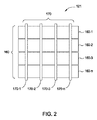
[0041]図2は、いくつかの実施形態に従い、パターンと関連付けられた検知領域において検知するように構成された検知要素121の例示的パターンの一部を示す。図示及び説明の明瞭性のために、図2は、簡略的な矩形のパターンの検知要素121を示し、種々の構成要素を示していない。検知要素121のこのパターンは、第1の複数のセンサ電極160(160−1、160−2、160−3、・・・160−n)、及び複数の送信電極160上に配された第2の複数のセンサ電極170(170−1、170−2、170−3、・・・170−n)を備える。一実施形態において、検知要素121のこのパターンは、複数の送信電極160(160−1、160−2、160−3、・・・160−n)、及び複数の送信電極160上に配された複数の受信電極170(170−1、170−2、170−3、・・・170−n)を備える。別の実施形態において、第1の複数のセンサ電極は、送信及び受信するように構成することができ、且つ、第2の複数のセンサ電極も送信及び受信するように構成することができる。
[0041] FIG. 2 illustrates a portion of an exemplary pattern of sensing
[0042]送信電極160及び受信電極170は、概して、互いからオーム性的に絶縁される。すなわち、1つ又は複数の絶縁体は、送信電極160と受信電極170とを隔て、且つ電極が互いと電気的に短絡することを防止する。いくつかの実施形態において、送信電極160及び受信電極170は交差箇所において送信電極160と受信電極170との間に配された絶縁材料によって離され、このような構成において、送信電極160及び/又は受信電極170は、同一電極の異なる部分を接続するジャンパと共に形成することができる。いくつかの実施形態において、送信電極160及び受信電極170は、絶縁材料の1つ又は複数の層によって離される。いくつかの実施形態において、送信電極160及び受信電極170は、1つ又は複数の基板によって離され、例えば、送信電極160及び受信電極170は、同一基板の反対側に、又は合わせて積層された異なる基板上に配することができる。
[0042] Transmit
[0043]送信電極160と受信電極170との間の局在化された容量結合の箇所は、「容量性画素」と称することができる。送信電極160と受信電極170との間の容量結合は、送信電極160及び受信電極170と関連付けられた検知領域における入力オブジェクトの近接及び動きによって変化する。
[0043] The location of localized capacitive coupling between the transmit
[0044]いくつかの実施形態において、センサパターンは、これらの容量結合を判定するように「走査」される。すなわち、送信電極160は、送信信号を送信するように制御される。送信装置は、1つの送信電極が1度に送信するように、又は複数の送信電極が同時に送信するように動作することができる。複数の送信電極が同時に送信する場合、これらの複数の送信電極は、同じ送信信号を送信することができ、且つ実際上、より大きな送信電極を効果的に生成することができ、又はこれらの複数の送信電極は、異なる送信信号を送信することができる。例えば、複数の送信電極は、結果として生じる受信電極170の信号に対する送信電極の結合された効果が独立的に判定されることを可能にする1つ又は複数の符号化体系に従い異なる送信信号を送信することができる。
[0044] In some embodiments, the sensor pattern is “scanned” to determine these capacitive couplings. That is, the
[0045]受信センサ電極170は、単独で又は複合的に動作して、結果として生じる信号を取得することができる。結果として生じる信号は、容量性画素において容量結合の大きさを判定するために使用することができる。
[0045] The receive
[0046]容量性画素からの測定値一式は、画素における容量結合の典型である「容量性画像」(「容量性フレーム」ともいう)を形成する。複数の容量性画像は、複数の時間区間上で取得することができ、且つ容量性画素間の差異は、検知領域における入力についての情報を引き出すことに使用される。例えば、連続した時間空間上で取得された連続した容量性画素は、検知領域に入る、検知領域から出ていく、及び検知領域内の1つ又は複数の入力オブジェクトの動き(複数可)を追跡するために使用することができる。 [0046] The set of measured values from the capacitive pixel forms a “capacitive image” (also referred to as a “capacitive frame”) that is typical of capacitive coupling at the pixel. Multiple capacitive images can be acquired over multiple time intervals, and differences between capacitive pixels are used to derive information about the input in the sensing region. For example, consecutive capacitive pixels acquired in a continuous time space enter the detection area, exit the detection area, and track the movement (s) of one or more input objects in the detection area Can be used to
[0047]センサ装置のバックグラウンド静電容量は、検知領域における非入力オブジェクトと関連付けられた容量性画像である。バックグラウンド静電容量は、環境及び動作状況によって変化し、且つ種々の方法で見積もることができる。例えば、いくつかの実施形態は、非入力オブジェクトが検知領域にあると判定されるとき「基準線画像」を取り、そして、バックグラウンド静電容量の見積もりとしてこれらの基準線画像を使用する。 [0047] The background capacitance of the sensor device is a capacitive image associated with a non-input object in the sensing region. Background capacitance varies with environment and operating conditions and can be estimated in various ways. For example, some embodiments take “baseline images” when it is determined that a non-input object is in the sensing region and use these baseline images as an estimate of background capacitance.
[0048]容量性画像は、より効率的な処理のために、センサ装置のバックグラウンド静電容量用に調節することができる。いくつかの実施形態は、容量性画素における容量結合の測定値を「基準線化」することによってこれを成し遂げ、「基準線化された容量性画像」を生成する。すなわち、いくつかの実施形態は、容量性画像を形成する測定値を、これらの画素と関連付けられた「基準線画像」の適切な「基準線値」と比較し、そして、基準線画像からの変化を判定する。 [0048] Capacitive images can be adjusted for the background capacitance of the sensor device for more efficient processing. Some embodiments accomplish this by “baselining” the capacitive coupling measurements at the capacitive pixel to produce a “baselined capacitive image”. That is, some embodiments compare the measurements that form the capacitive image with the appropriate “baseline value” of the “baseline image” associated with these pixels, and from the baseline image Determine change.
[0049]いくつかのタッチ画面実施形態において、送信電極160は、表示画面の表示を更新する際に使用される1つ又は複数の共通電極(例えば、「V−com電極」又はソース制御電極)を備える。これらの共通電極は、適切な表示画面基板上に配することができる。例えば、共通電極は、いくつかの表示画面におけるTFTガラス(例えば、インプレーンスイッチング(IPS)(In Plane Switching)又はプラントゥラインスイッチング(PLS)(Plan to Switching)、いくつかの表示画面の色フィルタガラスの底面(例えば、パターンドバーティカルアラインメント(PVA)(Patterned Vertical Alignment)又はマルチドメインバーティカルアラインメント(MVA)(Multi−domain Vertical Alignment))、等に配することができる。このような実施形態において、共通電極は、複数の機能を行うので、「兼用電極」とも呼ぶことができる。種々の実施形態において、各送信電極160は、1つ又は複数の共通電極を備える。他の実施形態において、少なくとも2つの送信電極160は少なくとも1つの共通電極を共有することができる。
[0049] In some touch screen embodiments, the transmit
[0050]種々のタッチ画面実施形態において、「容量性フレームレート」(連続する容量性画像が取得される速度)は同じ、又は「表示フレームレート」(表示画像が更新される速度、表示を更新して同じ画像を再表示することを含む)と異なっていてもよい。2つのレートが異なるいくつかの実施形態において、連続する容量性画像は、異なる表示更新状態にて取得され、且つ異なる表示更新状態は、取得される容量性画像に影響を与え得る。すなわち、表示更新は、特に、バックグラウンド静電容量性画像に影響を与える。したがって、表示更新が第1の状態であるときに第1の容量性画像が取得され、且つ表示更新が第2の状態であるときに第2の容量性画像が取得される場合、第1及び第2の容量性画像は、検知領域の変化のためではなく、表示更新状態と関連付けられたバックグラウンド静電容量性画像の差異のために異なり得る。このことは、容量性検知及び表示更新電極が互いに密接に近接している場合、又はこれらが共有されている(例えば、兼用電極)ときに起こりやすい。種々の実施形態において、容量性フレームレートは整数倍の表示フレームレートである。別の実施形態において、容量性フレームレートは、分数倍の表示フレームレートである。またさらなる実施形態において、容量性フレームレートは、いずれか分数又は整数の表示フレームレートとすることができる。 [0050] In various touch screen embodiments, "capacitive frame rate" (speed at which successive capacitive images are acquired) is the same, or "display frame rate" (speed at which display image is updated, update display) And the same image may be displayed again). In some embodiments where the two rates are different, successive capacitive images are acquired at different display update states, and different display update states can affect the acquired capacitive image. That is, the display update particularly affects the background capacitive image. Thus, if the first capacitive image is acquired when the display update is in the first state and the second capacitive image is acquired when the display update is in the second state, the first and The second capacitive image may differ due to differences in the background capacitive image associated with the display update state, not due to changes in the sensing area. This is likely to occur when the capacitive sensing and display update electrodes are in close proximity to each other or when they are shared (eg, dual-purpose electrodes). In various embodiments, the capacitive frame rate is an integer multiple display frame rate. In another embodiment, the capacitive frame rate is a fractional display frame rate. In still further embodiments, the capacitive frame rate can be any fractional or integer display frame rate.
[0051]説明の便宜上、特定の表示更新状態間にとられた容量性画像は、特定のフレームの種類であると考えられる。すなわち、特定のフレームの種類は、特定の容量性検知順序と特定の表示順序との対応付けと関連付けられる。したがって、第1の表示更新状態の間にとられた第1の容量性画像は、第1のフレームの種類と考えられ、第2の表示更新状態の間にとられた第2の容量性画像は、第2のフレームの種類と考えられ、第3の表示更新状態の間にとられた第3の容量性画像は、第3のフレームの種類と考えられ、以下同様である。表示更新状態及び容量性画像取得の関係が周期的である場合、取得された容量性画像は、フレームの種類によって循環され、そして再現される。いくつかの実施形態において、すべての表示更新状態のための「n」個の容量性画像が存在し得る。 [0051] For convenience of explanation, a capacitive image taken during a particular display update state is considered to be of a particular frame type. That is, a specific frame type is associated with a correspondence between a specific capacitive detection order and a specific display order. Accordingly, the first capacitive image taken during the first display update state is considered to be the first frame type and the second capacitive image taken during the second display update state. Is considered to be the second frame type, and the third capacitive image taken during the third display update state is considered to be the third frame type, and so on. If the relationship between the display update state and capacitive image acquisition is periodic, the acquired capacitive image is circulated and reproduced according to the frame type. In some embodiments, there may be “n” capacitive images for all display update states.
(表示行更新の間における容量性検知の実行)
[0052]図3は、本明細書に開示された一実施形態に従い、インターリーブされた容量性検知区間を有する、表示フレームを処理するタイミング図300である。詳細には、タイミング図300は、表示フレームにおける異なる時間区間を図示する。時間区間A〜D及びF〜Hは、それぞれ、入力装置における表示画面の1つの表示行を更新するために使用される時間を示す。この表示行更新時間は、表示行の画素310を更新するために使用される時間区間及び各表示行更新305間で生ずるバッファ時間315にさらに分割される。バッファ時間315は、水平空白区間315と称することもできる。制御モジュールは、水平空白区間315を使用して、例えば、次の表示行を更新するのに必要なデータを取り出す、表示行に対応する共通電極(複数可)で電圧を制御する、又は信号を安定させて、後の表示行を更新するときの干渉を低減させることができる。それにもかかわらず、本明細書に開示された実施形態は、水平空白区間315を有する入力装置に限定されず、画素更新区間310と次の表示行更新305との間のバッファ時間が存在しないシステムにおいて使用することができる。種々の実施形態において、水平空白時間315は、水平空白時間315が実質的に存在しないような長さに短縮される。他の実施形態において、水平空白時間315は、表示行を更新するように共通電極を構成するのに必要な時間の長さ以下となるような長さに短縮される。
(Performance detection during display row update)
[0052] FIG. 3 is a timing diagram 300 for processing a display frame with interleaved capacitive sensing intervals in accordance with one embodiment disclosed herein. In particular, the timing diagram 300 illustrates different time intervals in the display frame. The time intervals A to D and F to H indicate times used for updating one display line of the display screen in the input device, respectively. This display row update time is further divided into a time interval used to update the
[0053]さらに、共通電極0〜Nは、いずれかの順序で表示更新のために制御することができる。例えば、制御モジュールは、表示画面の上部の表示行を更新することができ、それに続く表示行更新305において、画面の下部の表示行を更新することができる。結果として、入力装置は、表示画面において連続して位置していない2つの共通電極を連続的に制御することができる。またさらに、例えば、表示画面の一部のみが情報をアクティブに表示している場合、表示フレームは、表示画面の各表示行を更新しなくてもよい。したがって、図300における共通電極0〜Nは、入力装置における共通電極の一部のみを表すことができる。
[0053] Further, the common electrodes 0-N can be controlled for display updates in any order. For example, the control module can update the display line at the top of the display screen, and can update the display line at the bottom of the screen in a subsequent
[0054]一実施形態において、時間区間Eは、容量性検知のための時間、又は容量性検知区間を表す。時間区間Eは、表示画面の1つの行を更新する時間と少なくとも同じ長さにすることができる。別の実施形態において、時間区間Eは、表示画面の1つの行を更新する時間よりも長い。さらに、入力装置は、表示画面の画素を更新するのに使用される同じ共通電極を使用して、送信信号を制御することができる。すなわち、共通電極は、二重の目的を受け持つことができる。表示更新区間の間、共通電極は、表示における画素を更新するが、容量性検知区間の間、共通電極は送信電極として使用される。 [0054] In one embodiment, time interval E represents a time for capacitive detection or a capacitive detection interval. The time interval E can be at least as long as the time for updating one row of the display screen. In another embodiment, time interval E is longer than the time to update one row of the display screen. Furthermore, the input device can control the transmission signal using the same common electrode used to update the pixels of the display screen. That is, the common electrode can serve a dual purpose. During the display update interval, the common electrode updates the pixels in the display, but during the capacitive sensing interval, the common electrode is used as the transmission electrode.
[0055]一実施形態において、時間区間A〜Dの間に表示行を更新した後、制御モジュールは、表示更新を休止すること、及び時間区間Eを使用して容量性検知を行うことができる。この時間区間の間、制御モジュールは、表示画面における画素のいずれかを更新しなくてもよい。加えて、制御モジュールは、表示画面における少なくとも1つの電極送信電極(例えば、少なくとも1つの共通電極)で送信信号を制御することができる。送信信号に対応する効果を含む、結果として生じた受信信号に基づいて、入力装置は、装置の検知領域に近接する入力オブジェクトの位置情報を引き出す。一実施形態において、入力装置は、送信信号を制御する共通電極と受信電極との間の容量結合の変化を測定する。そして、容量性変化は、入力オブジェクトの位置情報を引き出すために使用される。本明細書に提供された実施形態は、送信信号を送信する共通電極を使用することについて論じているけれども、他の実施形態においては、共通電極は、送信信号を制御する電極の代わりに、結果として生じる信号を受信する受信電極として使用することができる。例えば、入力装置は、結果として生じる信号を共通電極で発生させる送信信号を制御する別個の電極一式を含むことができる。またさらに、別の実施形態において、第1の共通電極一式は、送信信号を送信するように構成することができ、且つ第2の共通電極一式は、結果として生じる信号を受信するように構成することができる。種々の実施形態において、時間区間Eの間、送信電極は、容量性検知のために制御することができ、この場合、送信電極は、共通電極から独立している。 [0055] In one embodiment, after updating the display row during time intervals A to D, the control module can pause the display update and use time interval E to perform capacitive sensing. . During this time interval, the control module may not update any of the pixels on the display screen. In addition, the control module can control the transmission signal with at least one electrode transmission electrode (eg, at least one common electrode) on the display screen. Based on the resulting received signal, including the effect corresponding to the transmitted signal, the input device retrieves position information of the input object proximate to the sensing area of the device. In one embodiment, the input device measures the change in capacitive coupling between the common electrode that controls the transmitted signal and the receiving electrode. The capacitive change is then used to extract the position information of the input object. Although the embodiments provided herein discuss using a common electrode that transmits a transmission signal, in other embodiments, the common electrode is the result instead of the electrode that controls the transmission signal. Can be used as a receiving electrode for receiving a signal generated as follows. For example, the input device can include a separate set of electrodes that control the transmitted signal that causes the resulting signal to be generated at a common electrode. In yet another embodiment, the first set of common electrodes can be configured to transmit a transmission signal, and the second set of common electrodes is configured to receive the resulting signal. be able to. In various embodiments, during time interval E, the transmit electrode can be controlled for capacitive sensing, where the transmit electrode is independent of the common electrode.
[0056]一実施形態において、制御モジュールは、複数の連続した水平空白区間315の間、例えば、時間区間A〜D用の水平空白区間315の間で容量性検知を行う。各個別の水平空白区間315の間、静電容量の大きさを取得するために必要とされる情報の一部のみを捕捉することができる。水平空白区間315は、入力装置にとって短すぎるので、特定の送信電極のために正確な静電容量の大きさを引き出すことができないかもしれない。しかしながら、複数の水平空白区間315の間で容量性検知を行った後、入力装置は、選択された電極に関する容量結合の変化の正確な大きさを引き出すことができる。特定の電極に関する静電容量の大きさを得る検知周期が、各連続的な水平空白区間315の間、断続的に送信されるので、水平空白時間315の間のこのような容量性検知の方法は、本明細書において非連続的容量性検知と称される。異なる言い方をすれば、非連続的容量性検知は、1つの電極(又は選択された電極群)に関する容量性検知が2つ以上の不連続な時間区間にわたり継続するときに存在することができる。
[0056] In one embodiment, the control module performs capacitive sensing between a plurality of consecutive horizontal
[0057]あるいは又は加えて、制御モジュールは、容量性検知を行うために表示を更新することを休止することができる。図300に示すように、制御モジュールは、時間区間A〜Dの間、共通電極0〜3と関連付けられた画素を更新する。しかしながら、時間区間Eにおいて、表示更新は、容量性検知が行われる間休止される(すなわち、制御モジュールは、フレームにおける次の表示行の更新を継続しない)。詳細には、容量性検知区間320は表示フレームの表示行更新とインターリーブされる。したがって、容量性検知区間は、制御モジュールが容量性検知を行う間表示更新が休止されるフレーム内空白区間、長期水平空白区間、又は長期h−空白区間とも称することができる。制御モジュールは、容量性検知区間320が終わった後、同じ表示フレームのための表示更新を再開する。一実施形態において、容量性検知区間320は、水平空白区間315よりも長く、且つ、いくつかの実施形態において、画素更新区間310又は表示行更新305と少なくとも同じである。表示更新区間305と同じ長さであるとして示されているが、種々の実施形態において、容量性検知区間320は表示更新区間305よりも長くすることができる。示すように、時間区間Eは、図300における他の時間区間−すなわち、時間区間A〜D及びF〜H−の(水平方向及び垂直方向の矢印で示すように)3倍の長さである。しかしながら、容量性検知区間320の時間は、入力装置の特定の設計に応じて調節することができる。容量性検知区間320を行うことに加えて、一実施形態において、制御モジュールは、表示行更新305の1つ又は複数の水平空白区間315の間、容量性検知も行う。
[0057] Alternatively or additionally, the control module can pause updating the display to perform capacitive sensing. As shown in FIG. 300, the control module updates the pixels associated with the common electrodes 0 to 3 during the time intervals A to D. However, in time interval E, the display update is paused while capacitive sensing is performed (ie, the control module does not continue to update the next display line in the frame). Specifically, the
[0058]容量性検知区間320の間に容量性検知を生じさせることは、入力装置が、断続無しに選択された電極(すなわち、送信信号を制御する電極)に関する静電容量変化を正確に測定すること、又は干渉感受性を改善することを可能にし得る。したがって、容量結合の変化が、連続した時間区間において選択された電極又は電極群に関して測定されるので、容量性検知区間320の間に容量性検知を行うことは、本明細書において連続的容量検知と称される。
[0058] Generating capacitive sensing during
[0059]さらに、制御モジュールは、前の表示更新区間において使用された電極を使用して容量性検知を行うことができる。例えば、時間区間Eの間、制御モジュールは、共通電極0〜3で同時に送信信号を制御することができる。このようにして、制御モジュールは、1つ又は複数の共通電極を使用して表示行の画素を更新することができ、且つ表示フレームにおける他の表示行の更新を継続する前に、同じ電極を使用して容量性検知を行うことができる。 [0059] Further, the control module can perform capacitive sensing using the electrodes used in the previous display update interval. For example, during the time period E, the control module can control the transmission signals simultaneously with the common electrodes 0 to 3. In this way, the control module can update the pixels of the display row using one or more common electrodes, and the same electrode before continuing to update other display rows in the display frame. Capacitive sensing can be performed using.
[0060]表示更新が休止されたとき、制御モジュールは、送信信号を制御していない共通電極で信号をなお制御することができる。例えば、送信信号が1つ又は複数の電極で送信されている間、制御モジュールは、表示画面における他の共通電極に基準電圧(又は別の他の信号)を印加することができる。容量性検知用に現在使用されていない共通電極を基準電圧に固定することは、入力装置の能力を改善して、入力オブジェクトの正確な位置情報を引きだすことができる。したがって、表示更新が休止されるとき、制御モジュールは、表示画面の画素の更新を止めることができるが、容量性検知のために共通電極をなお使用することができる。 [0060] When the display update is paused, the control module can still control the signal with the common electrode not controlling the transmitted signal. For example, the control module can apply a reference voltage (or another signal) to the other common electrode on the display screen while the transmission signal is transmitted on one or more electrodes. Fixing a common electrode that is not currently used for capacitive sensing to a reference voltage can improve the capability of the input device and derive accurate position information of the input object. Thus, when the display update is paused, the control module can stop updating the pixels on the display screen, but can still use the common electrode for capacitive sensing.
[0061]垂直空白区間325は、表示フレームの最終表示行更新区間とそれに続く表示フレームの列更新区間の冒頭との間の区間である。図3には示されていないが、タイミング図300は、受信した表示フレームに基づく表示の更新の初めに、−すなわち時間区間Aの前に−、第2の垂直空白区間を含むこともできる。入力装置がこれらの垂直空白区間の間、表示を更新しないので、いくつかの実施形態において、制御モジュールは、第1又は第2の垂直空白区間のいずれか(又は両方)を使用して静電容量検知を行うこともできる。容量性検知区間320と同様に、これらの空白区間の両方が十分な長さの時間を提供して、重大な阻害なく、選択された共通電極と関連付けられた静電容量変化を測定することができるので、垂直空白区間325は、連続的容量性検知を容易にする。しかしながら、容量性検知区間320は同じ表示フレームの表記行更新間に挿入されているが、垂直空白区間325は表示フレームの冒頭又は末尾のいずれかに当たるので、垂直空白区間325は、容量性検知区間320とは区別される。
[0061] The vertical
[0062]多くの実施形態において、水平空白区間315、容量性検知区間320及び/又は垂直空白区間325の長さは変化させることができる。しかしながら、表示フレームレートは変化させることができないかもしれない。このため、これらの非表示更新区間の1つの長さが変化するに伴い、他の非表示更新区間の少なくとも1つも変化させることができる。例えば、容量性検知区間320が表示フレーム内に含まれている実施形態において、水平空白区間315及び/又は垂直空白区間325の時間は相応に短縮することができる。共通電極の第1のセットの表示行更新区間305に対応して水平空白区間315を短縮することによって、容量性検知区間320は表示フレーム内に挿入することができる。水平空白区間315の長さが「T」μsとしたとき、「M」個の対応共通電極について水平空白区間315を「N」μsに短縮することは、長さ「(T−N)*M」μsのフレーム内空白区間320を作出することができることを意味する。一実施形態において、T−Nは、水平空白区間315が必要な表示行更新手続きに十分な時間をなお提供するように短縮することができる。容量性検知区間320の時間は、各水平空白区間315の短縮の総計に基づくことができる。他の実施形態において、フレーム内空白区間315の時間は、垂直空白区間325を変化させることに基づくことができ、又は水平空白区間315及び垂直空白区間325の両方を変化させることに基づくことができる。
[0062] In many embodiments, the length of the horizontal
[0063]容量性検知区間320の時間は、例えば、共通電極の対応群に関して連続的容量性検知を行うこと、容量性検知と表示更新との間の切り替えから雑音を軽減すること、又は周波数ホッピングを行い又は容量性検知フレームレートを変更して雑音干渉を低減することに必要とされる時間量に応じて設定することができる。例えば、共通電極の一群に関して、100μsが連続的容量性検知のために必要とされ得る。したがって、対応する容量性検知区間320は、少なくとも長さが100μsとなるように決定される。所望のフレームレートをなお維持するが100μsを利用可能とするために、水平空白区間315の1つ若しくは複数又は垂直空白区間325は短縮することができる。
[0063] The time of
[0064]図3は、共通電極0〜Nが、表示を更新すること及び容量性検知を行うことの両方ために使用される実施形態において記載されていたが、この開示はこのようなものに限定されない。一実施形態において、たとえ送信信号が、表示を更新するときに使用されない電極で制御されたとしても、入力装置は、フレーム内空白区間を使用して容量性検知を行うことができる。表示更新のために使用される電極及び容量性検知のために使用される電極は、入力装置において密に近接し得るので、相互に排他的な時間区間において2つの機能を行うことは、異なる電極セット間の電気的干渉の大きさを低下させることができる。 [0064] Although FIG. 3 was described in an embodiment where the common electrodes 0-N are used for both updating the display and performing capacitive sensing, the disclosure is thus It is not limited. In one embodiment, the input device can perform capacitive sensing using intra-frame blank intervals even if the transmitted signal is controlled by an electrode that is not used when updating the display. Since the electrodes used for display update and the electrodes used for capacitive sensing can be in close proximity in the input device, performing two functions in mutually exclusive time intervals is different. The magnitude of electrical interference between sets can be reduced.
[0065]図4は、本明細書に開示された一実施形態に従い、容量性検知区間を表示フレーム更新にインターリーブするタイミングダイアグラムである。タイミングダイアグラム400は、図3に示す時間区間A〜Fの間に共通電極0〜5で伝搬された波形を含む。時間区間A〜Dの間において、制御モジュールは、共通電極の1つを作動させ、対応する表示行と関連付けられた画素を更新する。1つの電極が作動されている間、残りの電極は一定の電圧に維持することができる。さらに、共通電極は、示されるような各時間区間に瞬間的に切り替えられないかもしれない(例えば、電極1がオンに切り替わるとき、電極0はオフに切り替わる)。その代わりに、電極が急騰又は急降下するいくらかの遅延−例えば、水平空白区間−が存在することができる。種々の実施形態において、複数の共通電極は、遅延された態様で制御させることができ、この場合、第1の共通電極が作動され、その後いくらかの遅延の後、第2の共通電極が制御される。
[0065] FIG. 4 is a timing diagram for interleaving capacitive sensing intervals to display frame updates in accordance with one embodiment disclosed herein. Timing diagram 400 includes waveforms propagated at common electrodes 0-5 during time intervals A-F shown in FIG. During time intervals A-D, the control module activates one of the common electrodes and updates the pixel associated with the corresponding display row. While one electrode is activated, the remaining electrodes can be maintained at a constant voltage. Further, the common electrode may not be switched instantaneously during each time interval as shown (eg, when
[0066]時間区間Eの間、制御モジュールは表示更新を休止し、且つ容量性検知に切り替わる。図4において、1つ又は複数の共通電極は、送信信号(例えば、矩形波)が、送信電極に割り当てられる各共通電極で同時に送信される送信電極に分類される。例えば、表示装置は、数百の共通電極を含むことができるが、容量性検知を行うとき、装置は、各送信電極が単一の送信電極として扱われる送信電極(例えば、各40個の共通電極のうちおよそ20個の送信電極)に共通電極を分割することができる。別の実施形態において、共通電圧電極は、複数の共通電極に分割することができ、この場合、送信電極は1つの共通電極を備える。さらに、他の実施形態において、共通電圧電極は、いずれかの数の共通電極に分割することができ、この場合、いずれかの数の共通電極は、送信電極を形成するように結合することができる。単純化のために、図4は、共通電極0〜3が1つの送信電極に割り当てられ、且つ同一の送信信号によってそれぞれ制御される実施形態を図示する。あるいは、他の表示装置において、共通電極は、表示更新の間、同一の基準電圧に制御される複数の共通電極区分(共通電極)から構成される1つの電極「面」とすることができる。しかしながら、容量性検知の間、電極平面の異なる共通電極区分(すなわち、共通電極)は異なる時に送信信号を送信するために使用され、1つ又は複数の送信電極として機能する。 [0066] During time interval E, the control module pauses the display update and switches to capacitive detection. In FIG. 4, one or more common electrodes are classified as transmission electrodes in which a transmission signal (for example, a rectangular wave) is simultaneously transmitted by each common electrode assigned to the transmission electrode. For example, a display device can include hundreds of common electrodes, but when performing capacitive sensing, the device can transmit electrodes where each transmit electrode is treated as a single transmit electrode (eg, 40 commons each The common electrode can be divided into approximately 20 transmission electrodes). In another embodiment, the common voltage electrode can be divided into a plurality of common electrodes, in which case the transmit electrode comprises one common electrode. Further, in other embodiments, the common voltage electrode can be divided into any number of common electrodes, in which case any number of common electrodes can be combined to form a transmission electrode. it can. For simplicity, FIG. 4 illustrates an embodiment in which common electrodes 0-3 are assigned to one transmit electrode and are each controlled by the same transmit signal. Alternatively, in another display device, the common electrode may be a single electrode “plane” composed of a plurality of common electrode sections (common electrodes) controlled to the same reference voltage during display update. However, during capacitive sensing, different common electrode sections (ie, common electrodes) in the electrode plane are used to transmit transmitted signals at different times and function as one or more transmitting electrodes.
[0067]静電容量検知区間は、複数の検知周期410(又はタッチ周期)にさらに分割することができる。フレーム内空白区間を使用することは、電極ブロックと1つ又は複数の受信電極との間の静電容量変化を引き出すのに十分な複数の連続的検知周期を制御モジュールが制御することを可能にし得ることが有利である。例えば、入力装置が静電容量の変化を正確に測定するためには6つの検知周期410を行うが、水平空白区間315の間では2つの検知周期410のみを行うことができると仮定すると、制御モジュールは、各電極ブロックに関して少なくとも3つの水平空白区間315を使用しなければならない。逆に、図4に示すフレーム内空白区間320を用いて、入力装置は、検知周期410の間、表示を更新することなく6つの検知周期410を連続して測定する。
[0067] The capacitance detection section can be further divided into a plurality of detection periods 410 (or touch periods). Using an intra-frame blank interval allows the control module to control a plurality of consecutive sensing periods sufficient to derive a capacitance change between the electrode block and one or more receiving electrodes. It is advantageous to obtain. For example, assuming that the input device performs six
[0068]入力装置は、容量性検知区間320の間、6より多い又は6未満の周期を行うように構成できることは当然である。さらに、入力装置は、1つの容量性検知区間320の間に複数の送信電極で容量性検知を行うことができる。例えば、制御モジュールは、共通電極0〜3で、必要な検知周期410を制御することができ、そして、共通電極4〜7で必要な検知周期を制御することができる。またさらに、制御モジュールは、フレーム内空白区間320の間、静電容量検知に使用されない他の共通電極で電圧を制御することもできる。すなわち、他の共通電極(例えば、共通電極4及び5)の電圧が浮動状態になることを可能にする代わりに、制御モジュールは、これらの電極で実質的に一定の電圧(例えば、基準電圧)を制御することができる。
[0068] Of course, the input device can be configured to perform more than 6 or less than 6 periods during the
[0069]一実施形態において、入力装置は、容量性検知区間320の間、複数の送信電極で同時に送信信号を送信する。示されてはいないが、制御モジュールは、符号分割多重送信又は直交周波数分割多重送信等の多重送信方式に基づいて各送信電極で異なる送信信号を出力することができる。したがって、本明細書に開示された実施形態は、共通電極の下位セットで同じ送信信号を送信することに限定されないが、送信電極と受信電極との間の静電容量の変化を測定するために複数の送信電極で同時に異なる送信信号を送信することができる。
[0069] In one embodiment, the input device transmits a transmission signal simultaneously with a plurality of transmission electrodes during the
[0070]図5は、本明細書に開示された一実施形態に従い、インターリーブされた容量性検知区間を有する表示フレームを処理するタイミング図である。図3と対比すると、タイミング図500は、複数の容量性検知区間320を用いて1つの表示フレームを更新するタイミングを図示する。本明細書に使用されているように、複数のシーケンシャル表示行更新は表示更新クラスタ505として表記される。したがって、図3を参照すると、時間区間A〜Dの間で行われた表示行更新は、1つの表示更新クラスタ505として記載することができる。表示フレーム更新における各表示更新クラスタ505(又は容量性検知区間)は、同様の時間とすることができ、又は異なる時間を有することができる。さらに、表示更新クラスタ505における共通電極の数は、各容量性検知区間320における静電容量検知に使用される共通電極の数と同じとすることができ、又は使用される電極の数は異ならせることができる。
[0070] FIG. 5 is a timing diagram for processing a display frame having interleaved capacitive sensing intervals, according to one embodiment disclosed herein. In contrast to FIG. 3, timing diagram 500 illustrates the timing of updating one display frame using a plurality of
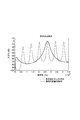
[0071]図6は、本明細書に開示された一実施形態に従い、表示更新と容量性検知との間で切り替えるときの雑音感受性を図示するグラフである。入力装置の干渉感受性は、フレーム内空白区間の間に容量性検知を行うことによって低減させることができる。フレーム内空白区間の間の容量性検知は、共通電極のブロックと受信電極との間の容量結合を見込んで連続的な態様で決定される。一実施形態において、干渉感受性は、入力オブジェクトの応答に関する周波数より低い周波数に低下される。さらに、フレーム内更新区間の間の容量性検知は、より少ない調波を有するより広いローブを有する周波数応答を提供することができる。一実施形態において、主ローブは、入力オブジェクトの周波数応答に近接する。図6は、非連続的容量性検知と連続的容量性検知の周波数感受性間の比較を図示する。示すように、非連続的容量性検知の周波数感受性は、より多くのピークを含み、これらのピークは、ピーク近くの入力オブジェクトの干渉感受性を増大させ得る。例えば、低周波数において、連続的容量性検知は、低周波数干渉に実質的に影響を受けないが、一方、非連続的容量性検知は、75kHz、140kHz、及び210kHzにおけるローブによって図示されるように、このような干渉に影響を受け得る。一実施形態において、外部電源は、低周波数干渉(例えば、200kHz未満)を導入することができる。このような実施形態において、フレーム空白区間の間で共通電極を用いる容量性検知(連続的容量性検知)の送信信号は、このような干渉に対する感受性を低下させる。 [0071] FIG. 6 is a graph illustrating noise sensitivity when switching between display update and capacitive sensing, according to one embodiment disclosed herein. The interference sensitivity of the input device can be reduced by performing capacitive detection during the blank period in the frame. Capacitive sensing during the in-frame blank interval is determined in a continuous manner, allowing for capacitive coupling between the common electrode block and the receiving electrode. In one embodiment, the interference sensitivity is reduced to a frequency that is lower than the frequency associated with the response of the input object. Furthermore, capacitive sensing during the intra-frame update interval can provide a frequency response with a wider lobe with less harmonics. In one embodiment, the main lobe is close to the frequency response of the input object. FIG. 6 illustrates a comparison between the frequency sensitivity of discontinuous capacitive detection and continuous capacitive detection. As shown, the frequency sensitivity of discontinuous capacitive sensing includes more peaks, which can increase the interference sensitivity of input objects near the peaks. For example, at low frequencies, continuous capacitive sensing is substantially unaffected by low frequency interference, whereas non-continuous capacitive sensing is as illustrated by lobes at 75 kHz, 140 kHz, and 210 kHz. Can be affected by such interference. In one embodiment, the external power source can introduce low frequency interference (eg, less than 200 kHz). In such an embodiment, the capacitive sensing (continuous capacitive sensing) transmission signal using a common electrode between frame blank intervals reduces the sensitivity to such interference.
[0072]一実施形態において、入力装置は、入力装置が共通電極で送信信号を送信するのに使用する周波数をシフトさせることができる。例えば、共通電極は、フレーム内空白区間の間で容量性検知用の第1の送信信号を送信するように構成され、第1の送信信号は、第1の送信周波数を有する。第1の送信周波数における干渉測定に応答して、制御モジュールは、共通電極での第1の送信周波数とは異なる第2の周波数を有する第2の送信信号を制御することができる。入力装置は、検知された干渉と、1つ又は複数の閾値とを比較し、そして、干渉が閾値のうちの1つを満たす又は超えるとき第1の周波数から第2の周波数(又は第2の周波数から第1の周波数へ戻る)へと切り替えることができる。さらに、第2の送信信号は、第1の送信信号とは異なる振幅、相、極性、周波数及び波形のうちの少なくとも1つを含むことができる。第1又は第2の送信信号のいずれかの波形は、矩形波形、三角波形、鋸歯波形、正弦波形、又はその他のうちの1つとすることができる。さらに、フレーム内空白区間の長さは、周波数ホッピングを収容するように調節することができる。すなわち、表示フレームにおいて使用される、フレーム内空白区間と表示更新との時間比は、異なる送信信号に切り替えるために変化させることができる。一実施形態において、フレーム内空白区間は、異なる周波数を有する送信信号に切り替えるために長くする必要があり、処理システムは、空白区間をそれに続くフレームに移動させて、最低限の表示画面更新レートを維持することができる。 [0072] In one embodiment, the input device can shift the frequency that the input device uses to transmit the transmitted signal at the common electrode. For example, the common electrode is configured to transmit a first transmission signal for capacitive detection between blank intervals in the frame, and the first transmission signal has a first transmission frequency. In response to the interference measurement at the first transmission frequency, the control module can control a second transmission signal having a second frequency different from the first transmission frequency at the common electrode. The input device compares the detected interference to one or more thresholds and from the first frequency to the second frequency (or second) when the interference meets or exceeds one of the thresholds. Switching from the frequency back to the first frequency). Further, the second transmission signal can include at least one of amplitude, phase, polarity, frequency, and waveform different from the first transmission signal. The waveform of either the first or second transmission signal can be one of a rectangular waveform, a triangular waveform, a sawtooth waveform, a sine waveform, or others. Further, the length of the intra-frame blank interval can be adjusted to accommodate frequency hopping. That is, the time ratio between the blank interval in the frame and the display update used in the display frame can be changed to switch to a different transmission signal. In one embodiment, the intra-frame blank interval needs to be lengthened to switch to a transmission signal having a different frequency, and the processing system moves the blank interval to the following frame to minimize the display screen update rate. Can be maintained.
[0073]一実施形態において、受信電極は、フレーム内空白区間の少なくとも一部の間で、結果として生じる干渉信号を受信するように構成することができる。この時間の間、共通電極(複数可)は、浮動状態にする、又は特定のDC電圧に連結することができる。そして、これらの干渉信号は、どの周波数信号(すなわち、どの周波数)を送信するかを決定するために使用することができる。送信信号は、干渉が低減することができるように、結果として生じる干渉信号に基づいて選択される。 [0073] In one embodiment, the receive electrode may be configured to receive the resulting interference signal during at least a portion of the intra-frame gap interval. During this time, the common electrode (s) can be floated or coupled to a specific DC voltage. These interference signals can then be used to determine which frequency signal (ie which frequency) to transmit. The transmitted signal is selected based on the resulting interference signal so that the interference can be reduced.
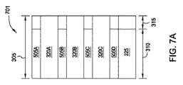
[0074]図7A〜図7Cは、本明細書に開示された実施形態に従い、インターリーブされた容量性検知区間で表示フレームを処理するタイミング図である。詳細には、図7Aは、第1の表示フレームのタイミング図701を図示する。図5のタイミング図と同様に、図701は、複数の表示行更新区間305を含み、それぞれは、画素更新区間310及び水平空白区間315を含み、複数の表示更新クラスタ505を形成するように分けられている。これらのクラスタ505は、複数の容量性検知区間でインターリーブされる。クラスタ505の時間は、容量性検知区間320の時間と関連してもよいし、又は関連しなくてもよい。例えば、入力装置は、所定の比に基づいて(垂直又は水平空白区間を調節することによって)クラスタ505及び容量性検知区間320の時間を設定することができる。あるいは、容量性検知区間320の時間は、クラスタ505の時間に関係なく、又は非連続的容量性検知を行うことから生じ得る雑音を緩和することにもっぱら基づいて、独立的に設定することができる。
[0074] FIGS. 7A-7C are timing diagrams for processing a display frame in an interleaved capacitive sensing interval in accordance with embodiments disclosed herein. Specifically, FIG. 7A illustrates a timing diagram 701 for the first display frame. Similar to the timing diagram of FIG. 5, FIG. 701 includes a plurality of display
[0075]表示画面は、表示更新クラスタ505A〜Dの間に表示行を更新することによって表示フレームに基づいて更新される。しかしながら、制御モジュールは、各クラスタ505A〜Cの後に表示を更新することを休止して、容量性検知区間320A〜Cの間に静電容量検知を行う。例えば、入力装置は、表示更新クラスタ505Aにおいて電極と関連付けられた画素を更新することができ、続いて、容量性検知区間320Aの間に、それらと同じ電極で静電容量検知を行うことができる。あるいは、制御モジュールは、前の表示更新クラスタ505において更新されなかった少なくとも1つの電極で静電容量検知を行うことができる。干渉を低減するために、一実施形態において、制御モジュールは、近時に更新された表示行とは異なる表示画面の一部における電極で静電容量検知を行う。これにより、表示を更新することが休止され、そして静電容量検知が開示した後でさえ、共通電極に一時的に影響を与える電気的干渉(静電容量、インダクタンス、及びその他)を回避することができる。
[0075] The display screen is updated based on the display frame by updating the display rows between the
[0076]図7B〜7Cは、図7Aに示される第1の表示フレームの後受信された第2の表示フレームに基づいて表示画面を更新するタイミング図702、703の2つの異なる実施形態を図示する。すなわち、図7B及び図7Cは、タイミング図が各後のフレームについて変化させることができることを図示する。一実施形態において、表示更新に容量性検知をインターリーブすることに起因する表示画像内の視覚的乱れは、表示フレームから表示フレームへ容量性検知区間の性質を改変することによって減少させることができる。この改変は、無作為的又は非無作為的な方法で行うことができる。 [0076] FIGS. 7B-7C illustrate two different embodiments of timing diagrams 702, 703 for updating a display screen based on a second display frame received after the first display frame shown in FIG. 7A. To do. That is, FIGS. 7B and 7C illustrate that the timing diagram can be changed for each subsequent frame. In one embodiment, visual disturbances in the display image due to interleaving capacitive sensing for display updates can be reduced by modifying the nature of the capacitive sensing interval from display frame to display frame. This modification can be done in a random or non-random manner.
[0077]図7Bは、図7Aに示されるクラスタ505A〜D及び容量性検知区間320A〜Cに関連する表示更新クラスタ505E〜G及び容量性検知区間320E〜Hを移動することを図示する。タイミング図701及び702の総時間は同じであるが、この時間を異なる区間にどのように分割するかは変えることができる。例えば、表示更新クラスタ505で開始する代わりに、タイミング図702は、垂直空白区間325(又は垂直空白区間325の一部のみ)を表示フレーム更新の冒頭に動かすことができる。前述したように、入力装置は、垂直空白区間325の間に静電容量検知を行うことができる。しかしながら、異なる表示更新クラスタ505E〜G間のタイミングは、同じままとすることができる。すなわち、表示更新クラスタ505を隔てる容量性検知区間320E〜Gの時間は、容量性検知区間320A〜Cの時間に対して維持される。このようにすることによって、制御モジュールと、表示フレームをドライバへ送信する動画源との間のタイミングを維持することができ、なお視覚的乱れを防止又は除去することができる。
[0077] FIG. 7B illustrates moving display update clusters 505E-G and
[0078]図7Cは、個別の表示更新クラスタ505及び容量性検知区間320の時間が、後のフレーム間で−すなわち、図7Aに示される第1のフレームと図7Cに示される第2のフレームとの間で−変化させることができることを図示する。例えば、表示更新クラスタ505Iは、タイミング図701の表示更新クラスタ505Aと同じタイミング図702の位置で開始するが、容量性検知区間320Iの時間は、空白区間320Aに対して増加する。一実施形態において、容量性検知区間320Iの追加された長さは、1つ又は複数の水平空白区間315及び垂直空白区間325を短縮すること、又は対応する水平空白区間315の数を増加することから生じさせることができる。あるいは、図7Cに示すように、入力装置は、タイミング図701において示される3つの容量性検知区間320A〜Cの代わりに、2つの容量性検知区間320I及び320Jのみを使用する。フレーム内空白区間のうちの1つを除去することによって節約された余りの時間は、残存する容量性検知区間320の1つ又は両方を延長するために使用することができる。さらに、空白区間320の拡大は、表示更新クラスタ505間の時間分離を内在的に拡大させる。この間隔を変更することは、視覚的乱れを防止又は除去することに寄与することができる。
[0078] FIG. 7C shows that the time of the individual
[0079]タイミング図703は、図7Aに示されるクラスタの1つを除去すること、及び余りの時間を、残存する表示更新クラスタ505I〜Kに追加することによって表示更新クラスタ505の時間を長くすることも図示する。ここで、クラスタ505Jの時間は、他のクラスタ505I及び505Kの時間の2倍まで延長される。このようにして、入力装置は、前の表示フレームにおいて使用される表示更新クラスタ505A〜Dに関連して表示更新クラスタ505I〜Kをさらに再配置することができる。
[0079] Timing diagram 703 extends the time of
[0080]非連続的な容量性検知を行う入力装置に関連する雑音を緩和することに加えて、図7A〜Cは、表示更新クラスタ及び容量性検知区間320を再配置又は変更して視覚的乱れを防止又は除去する異なる技法を図示するが、しかしながら、この開示は、これらの技法のみに限定されず、視覚的乱れを防止する他の技法に頼ることもできる。さらなる実施形態において、フレーム内空白区間の位置は、表示フレームから表示フレームへと無作為に変更することができる。さらに、容量性検知区間の開始前に表示を更新するために制御される共通電極又は次の容量性検知区間のために制御される共通電極は、表示フレームから表示フレームへと変化させることができる。さらに、容量性検知区間320の長さは、表示フレームのすべての容量性検知区間が同じ長さとはならないように、表示フレーム内で変更することができる。
[0080] In addition to mitigating noise associated with input devices that perform non-continuous capacitive sensing, FIGS. 7A-C can be used to visually reposition or modify the display update cluster and
[0081]図8は、本明細書に開示された実施形態に従い、表示更新に静電容量検知の区間をインターリーブする方法を図示する。方法800は、フレームデータに基づいて表示画面の画素を更新する処理システムに表示フレームを送信する動画源を用いてステップ805で開始する。動画源は、大きなまとまりとして−すなわち、一度にすべてのデータ−又は断続的に−すなわち、表示フレームの小さなまとまりが間隔をもって送信される−のいずれかで表示フレームを送信することができる。
[0081] FIG. 8 illustrates a method of interleaving capacitive sensing intervals for display updates in accordance with embodiments disclosed herein. The
[0082]ステップ810において、処理システムの制御モジュールは、受信した表示フレームデータに基づいて表示画面の1つ又は複数の表示行を更新する。制御モジュールは、例えば、表示画面において画素を更新する電界を発生するための共通電極を含む電極一式を使用することができる。表示行更新の間、制御モジュールは、少なくとも1つの共通電極を選択し、そして当該電極と関連付けられた画素を更新する。いくつかの実施形態において、表示画面は、異なる色画素を各共通電極と関連付けることができる。したがって、制御モジュールは、1つの共通電極を使用して複数の表示更新−例えば、赤、緑、及び青画素の更新−を行うことができる。
[0082] In
[0083]ステップ815において、表示更新は、フレーム内空白区間の間休止することができる。一実施形態において、表示更新を休止することは、結果として制御モジュールが表示画面において画素を更新することを止めることになる。表示を更新することの代わりに、ステップ820において、制御モジュール(又は異なる回路構成モジュール)は、共通電極を使用して静電容量検知を行うことができる。制御モジュールは、共通電極のうちの少なくとも1つ(又は送信電極)で送信信号を制御する。送信信号は、1つ又は複数の受信電極で、結果として生じる信号を発生させる。タッチ検出モジュールは、結果として生じる信号を使用して、入力装置のタッチ感応箇所近くの入力オブジェクトについての位置情報を引き出すことができる。一実施形態において、タッチ検出モジュールは、共通電極と受信電極との間の静電容量又は静電容量の変化を測定する。
[0083] In
[0084]一実施形態において、容量性検知区間の時間は、画素更新区間又は表示行更新区間と少なくとも同じ長さとすることができる。例えば、容量性検知区間の時間は、1つ又は複数の共通電極及び受信電極に関する静電容量の変化を判定するのに必要とされる検知周期の数に応じて設定することができる。別の言い方をすれば、入力装置は、共通電極に関する静電容量の正確な測定が検知周期を連続的に−すなわち、実質的な中断なく−送信することによって得ることができるように、フレーム内空白区間の時間を設定することができる。例えば、制御モジュールが静電容量の大きさを正確に得るために10個の検知周期を必要とする場合、容量性検知区間の時間は、10個の周期を行うのに少なくとも十分な長さである。 [0084] In one embodiment, the time of the capacitive sensing interval may be at least as long as the pixel update interval or the display row update interval. For example, the time of the capacitive sensing interval can be set according to the number of sensing cycles required to determine the change in capacitance for one or more common electrodes and receiving electrodes. In other words, the input device can be used within the frame so that an accurate measurement of the capacitance with respect to the common electrode can be obtained by transmitting the detection period continuously--that is, without substantial interruption. You can set the time of the blank section. For example, if the control module requires 10 detection cycles to accurately obtain the magnitude of the capacitance, the capacitive detection interval time is at least long enough to perform 10 cycles. is there.
[0085]ステップ825において、処理システムは、表示を更新することを再開することができる。詳細には、処理システムは、表示フレームデータに基づいて追加の表示行を更新する。さらに、処理システムは、全表示フレームが同時に送信されない実施形態において表示フレームの追加的一部を受信することができる。
[0085] At
(表示装置の例)
[0086]図9は、本明細書に開示された一実施形態に従い、電子システムと、表示更新区間に容量性検知区間をインターリーブする入力装置との間で通信するシステムを図示する。入力装置100は、電子システム150、及び組み込まれた検知装置を含む表示装置101を含む。図1に関して述べたように、電子システム150は、情報を電子的に処理することができるいずれかのシステムを幅広く指す。電子システム150のいくつかの非限定例には、デスクトップ型コンピュータ、ノート型コンピュータ、ネットブック型コンピュータ、タブレット、ウェブブラウザ、電子書籍読み取り装置、及び携帯情報端末(PDA)等、あらゆる大きさ及び形状のパソコンが含まれる。電子システム150は、表示のために入力装置100にデータを送信するグラフィックスプロセッサ905を含む。詳細には、グラフィックスプロセッサ905は表示フレームを入力装置100に送信し、且つ、これ自体、動画源と表記することができる。プロセッサ905は、表示データを発生するいずれかの適当なプロセッサであり、そして、複数のプロセッサ、マルチコアプロセッサ、及びその他を含むことができる。グラフィックスプロセッサ905は、グラフィックス処理を行う専用プロセッサ又は多目的プロセッサとすることができる。
(Example of display device)
[0086] FIG. 9 illustrates a system for communicating between an electronic system and an input device that interleaves a capacitive sensing interval with a display update interval, in accordance with one embodiment disclosed herein. The
[0087]入力装置100は、一実施形態において、電子システム150から送信された表示データを受信及び処理することに加えて、電子システム150に入力を供給するように構成することができる。入力装置100は、表示画面930及び処理システム110を含む。表示画面930は、グラフィックスプロセッサ905から受信した表示フレームに基づいて更新される1つ又は複数の表示行として配列された複数の画素を含む。電子システム150は、表示フレームにおいて、水平及び垂直空白区間のための組み込み区間を含む。処理システム110は、これらの組み込みタイミング区間を変更又は再配分して、上記で論じたフレーム内空白区間を発生させることができる。例えば、表示フレームが各水平空白区間に100μsを指定する場合、処理システム110は、各水平空白区間から90μsを使用して、表示フレーム更新に1つ又は複数のフレーム内空白区間を挿入することができる。
[0087] The
[0088]処理システム110は、入力装置100のハードウェアを動作させて、検知領域−例えば、表示画面930のある部分−における入力を検知するように構成することができる。処理システム110は、1つ又は複数の集積回路(IC)及び/又は他の回路構成要素のうちの一部又はすべてを備える。示すように、一実施形態において、処理システム110は、少なくとも、表示制御モジュール910、バッファ915、タッチ制御モジュール920、及び通信インターフェース925を含む。通信インターフェースは、電子システム150に、より詳細には、接続940を介してグラフィックスプロセッサ905に通信可能に結合される。通信インターフェース925は、バッファ915に記憶されるグラフィックスプロセッサ905からの表示フレームを受信する。しかしながら、いくつかの実施形態において、入力装置は、受信された表示フレーム部分を記憶する一時記憶装置必要としないことができ(すなわち、フレームデータは、受信されるのと同じ速さで処理される)、このため、バッファ915は省略することができる。インターフェース925は、以下により詳細に論じられる1つ又は複数の異なる制御信号を使用する電子システム150と通信することができる。一実施形態において、通信インターフェース925は、バス、ネットワーク、又は他の有線若しくは無線相互接続を使用する接続940に沿って、電子システムへデータを送信することができると共に、電子システムからデータを受信することができる。
[0088] The
[0089]処理システム110は、バッファ915を使用して、グラフィックスプロセッサ905から受信した表示フレームを一時的に記憶することができる。バッファ915は、ランダムアクセスメモリ(RAM)、複数の双方向ラッチメモリ素子、消去可能プログラマブル読み出し専用メモリ(EPROM又はフラッシュメモリ)、及びその他等のいずれかのメモリ記憶素子とすることができる。さらに、バッファ915は、1つのICに、処理システム110における他の要素のすべてと共に組み込むことができ、又は「チップ外部」に配置され、そして、処理システム110の他の構成要素と通信可能に結合することができる。さらに他の実施形態において、バッファ915は、電子システム120の一部として、及び/又はグラフィックスプロセッサ905の一部として組み込むことができる。バッファ915は、少なくとも1つの表示フレームを記憶するのに十分な記憶容量を有するように作製することができる。別の言い方をすれば、バッファ915は、表示画面930において各画素を更新するのに十分なデータを記憶することが可能である。処理システム110が表示バッファに基づいて表示画面930の更新を終えるとき、バッファ915は、グラフィックスプロセッサ905から送信された別の表示フレームによって消去又は書き換えることができる。
[0089]
[0090]あるいは、バッファ915は、表示フレームの一部のみ−すなわち、表示フレームにおける表示行更新の一部を行うのに十分なデータのみ−を記憶する能力を有してもよい。この実施形態において、グラフィックスプロセッサ905は、表示フレームの個別のまとまりを処理システム110に送信することができる。グラフィックスプロセッサ905は、例えば、バッファ915に記憶された表示フレームのまとまり(例えば、10個の表示行更新に対応するデータ)を移動し、処理システム110がデータに基づいて表示を更新するのを待って、そして処理システム110が追加データを要求した後に追加のまとまり−例えば、10個のさらなる表示行−を送信することができる。しかしながら、これは、処理システム110が表示画面930を更新することができるよりも速く接続940がデータを送信することができることを前提とする。そうでない場合には、バッファ915は、表示930を更新するためにすでに使用されたデータを、電子システム150から受信した新しいデータと絶えず交換することができる。すなわち、接続940は、データを一気に送信するのではなく、データを絶えず送信している。
[0090] Alternatively, the
[0091]表示制御モジュール910は、共通電極935を制御する回路構成を含むことができる。処理システム110は、表示画面930がグラフィックスプロセッサ905から受信した表示フレームに基づいて更新されるように、表示制御モジュール910を制御することができる。すなわち、表示制御モジュール910は、バッファ915に記憶された情報を使用して、表示画面930において画素を更新する。入力装置100において、表示制御モジュール910は、共通電極のみに接続されるが、モジュール910は、共通電極935と連携して制御される第2の対応する電極一式又はトランジスタに結合されて画素を更新することもできる。
[0091] The
[0092]処理システム110は、容量性検知を行うタッチ制御モジュール920を含む。処理システムは、表示制御モジュール910とタッチ制御モジュール920との間で共通電極935の制御を切り替える能力も有する。2つの別個の要素として示されているが、表示制御モジュール910の回路構成要素又はファームウェア及びタッチ制御モジュール920の回路構成要素又はファームウェアは、1つの要素に結合すること又は1つの処理システムICに組み込むことができる。処理システム110が表示更新を一旦休止すると、タッチ制御モジュール920は、共通電極と受信電極(不図示)との間の静電容量の変化を検出する共通電極935で送信信号を制御する。静電容量検知がフレーム内更新区間の間で起こる場合、静電容量検知(又は静電容量検知の一部)が一旦完了すると、処理システム110は、表示制御モジュール910を使用して、受信した表示フレームに基づいて表示画面930の更新を再開する。
[0092] The
[0093]処理システム110及び電子システム150は、1つ又は複数の制御信号を使用して、どのように又はいつ表示フレームを送信するかを通信及び調整することができる。たとえ処理システム110が最も早いデータビットレートと同じレートで表示を更新することができないとしても、接続940が表示フレームを処理システム110に最も早いデータビットレートで送信するように、表示ドライバ101を設計することができる。可能な限り大きなデータを送信することは、接続940が使用される時間を最小限にすることができ、これによって入力装置100の電池寿命を延ばすことができる。
[0093] The
[0094]一実施形態において、処理システム110は、制御信号を使用して、電子システム150及び処理システム110からの表示フレームデータの流れを休止することができる。電子システム150は、バッファ915から処理されたデータの量を含む処理システム110からの状態標識信号を受信することができる。例えば、処理システム110は、状態信号を使用して、バッファ915におけるデータのどれくらいが処理されたかを電子システム150に通知することができる。例えば、バッファ915が20個の表示行を更新するのに十分なデータを保持する場合、処理システム110は、19個の表示行が更新されたときに状態標識を使用して警報を送信することができる。電子システム150は、警報を使用して、予測される表示フレームレートを外挿法により推定することができる。すなわち、警報が予測可能な間隔で到達する場合、電子システム150は、処理システム110に表示フレームを送信するレート−例えば、100μs毎に表示フレームの20個の行を送信する−を推定することができる。このため、たとえ状態信号がもはや送信されないとしても、電子システム150は、推定されたレートを使用して、更新された表示データの送信を継続することができる。あるいは、電子システム150又は処理システム110は、あるレートで動作するように予め構成することができ、このため、状態信号は必要とされない。
[0094] In one embodiment, the
[0095]しかしながら、推定されたレートは、表示更新が休止されてフレーム内空白区間の間に静電容量検知を行うとき、バッファ915にアンダーフロー又はオーバーフローを生じさせるかもしれない。例えば、図7B及び7Cは、後の表示フレームにおいて表示更新クラスタ505及び容量性検知区間320を再配置することを示す。図7Bを参照すると、表示フレームは表示更新クラスタで開始しないので、電子システム150が、オーバーフローを生じさせるかもしれない、バッファ915のフレームデータをまだ処理していなかったとしても、接続940を使用して追加フレームデータを送信することができる。あるいは、図7Cを参照すると、表示更新クラスタ505Jは第1のフレームにおける他のクラスタ505A〜Dよりも長い時間を有する。したがって、処理システム110は、表示制御モジュール910がバッファ915におけるデータを放出し、結果としてアンダーフローを生ずるときでさえ、表示更新クラスタ505Jの間に表示画面を更新することをなお試みることができる。したがって、処理システム110及び電子システム150は、バッファのアンダーフロー及びオーバーフローを軽減又は防止するために、推定されたレートを変更する又は異なる通信技法を使用する必要があり得る。
[0095] However, the estimated rate may cause the
[0096]一実施形態において、処理信号110は、状態信号を使用して表示更新を休止することによってアンダーフロー又はオーバーフローを防止することができる。例えば、処理システム110は、表示更新クラスタ区間とフレーム内ブロック区間との間をいつ切り換えるのかを決定する論理を含むことができる。静電容量検知を開始することを一旦決定すると、処理システムは、状態信号に応答して更新を送信することを止める。この実施形態において、電子システム150は、推定されたレートを頼らずに、表示フレームをいつ送信するかを決定し、そしてその代わりに、状態信号で警報を受信することに応答して表示フレームを送信する。一実施形態において、処理システム110は、共通電極935の制御をタッチ制御モジュール920へ切り替えること及び状態信号でバッファの使用の更新を送信することを止めることによって表示更新を休止する。更新又は警報を受信することなく、グラフィックスプロセッサ905は、表示フレーム、又は表示フレームの一部を処理システム110に送信することを一時的に停止する。処理システム110が、表示の更新を再開することを決定すると−すなわち、フレーム内ブロック区間が完了した又は完了しようとしていると−、状態信号は、部分(又は全部)表示フレームを処理システム110に送信することによって応答する電子システム150に警報を送信することができる。待ち時間又は他の処理時間のために、フレーム内空白区間が一旦完了すると表示行更新を開始することができることを確保するため、フレーム内空白区間が終える前に、処理システム110は、電子システム150にさらなる表示フレームデータを送信することを命令することができる。処理システム110が、フレームデータの送信を休止することを電子システム150に命令する、異なる又は別個の制御信号を使用することができることを留意すべきである。例えば、処理システム110は、状態信号を使用してバッファの使用の更新を送信することを継続することができるであろうが、電子システム150が第2の制御信号を使用してさらなるデータを送信することを防止することができるであろう。表示更新クラスタ及びフレーム内ブロック区間の配置及び時間が後のフレーム間で変化するときでさえ、電子システム150からのフレームデータの流れを絞ることは、バッファ915の大きさを最小限にすることができる。
[0096] In one embodiment, the
[0097]別の実施形態において、電子システム150は、表示の更新をいつ休止するか−すなわち、フレーム内空白区間をいつ挿入するか−を制御することができる。例えば、グラフィックスプロセッサ905は、処理システム110が、表示制御モジュール910を使用して表示を更新することと、タッチ制御モジュール920を使用して静電容量検知を行うこととを切り替えるときを制御する必要な論理を有することができる。この実施形態において、電子システム150は、表示更新クラスタ及びフレーム内空白区間の配置を制御するので、状態信号は必要としないことができる。例えば、プロセッサ905は、処理システム110が表示フレームの一部−例えば、1つの表示行−を更新するのに必要とされる時間の長さ及びバッファ915の大きさがメモリに記憶されるように、再構成することができる。この知識に基づいて、バッファがアンダーフロー又はオーバーフローを経験することを防止する方法で、電子システム150は、1つのまとまり又は断続的な部分のいずれかとしての表示フレームを処理システム110に送信することができる。さらに、視覚的乱れを防止するために、グラフィックスプロセッサ905の論理は、表示フレームにおける表示更新クラスタ及びフレーム内空白区間の配置及び/又は時間を変化させることができる。乱れを防止する選択された技法に基づいて、グラフィックスプロセッサ905は、制御信号を使用してディスプレイの更新を休止する。すなわち、制御信号は、共通電極935の制御を表示制御モジュール910からタッチ制御モジュール920に切り替えることを処理システム110に命令する。
[0097] In another embodiment, the
(結論)
[0098]表示画面を有する入力装置は、表示行における画素に対応する共通電極を選択的に制御させることによって周期的に画面を更新(リフレッシュ)する。一般に、入力装置は、表示フレームの各表示行(及び各画素)が更新されるまで各電極を制御させる。表示を更新することに加えて、入力装置は、近接検知箇所として表示画面を使用する容量性検知を行うことができる。これを行うために、入力装置は、表示フレームに基づいて表示を更新する区間の間に容量性検知の区間をインターリーブすることができる。例えば、入力装置は、表示画面の表示行の第1の半分部分を更新し、表示更新を休止し、容量性検知を行い、及び表示行の残部の更新を終了することができる。このようにして、1つの表示フレームに基づいて画面を更新することに必要な時間区間は、容量性検知の1つ又は複数のインターリーブされた区間を含む。またさらに、入力装置は、表示を更新すること及び容量性検知を行うことの両方のために共通電極を使用することができる。
(Conclusion)
[0098] An input device having a display screen periodically updates (refreshes) the screen by selectively controlling common electrodes corresponding to pixels in the display row. Generally, the input device controls each electrode until each display row (and each pixel) of the display frame is updated. In addition to updating the display, the input device can perform capacitive detection using the display screen as a proximity detection location. In order to do this, the input device can interleave the capacitive sensing interval between intervals for updating the display based on the display frame. For example, the input device can update the first half of the display line of the display screen, pause the display update, perform capacitive detection, and finish updating the remainder of the display line. In this way, the time interval required to update the screen based on one display frame includes one or more interleaved intervals for capacitive detection. Still further, the input device can use a common electrode for both updating the display and performing capacitive sensing.
[0099]本明細書に述べられた実施形態は、本技法及びその特定の適用に従い実施形態を最も分かりやすく説明するため、及びこれによって当業者が本発明を実施及び使用できるようにするために提示された。しかしながら、当業者であれば、前述の説明及び例が、図示及び例示の目的のためだけに提示されたことを理解するであろう。記述したような説明は、網羅的であること又は開示された通りの形態に本発明を限定することを意図するものではない。 [0099] The embodiments described herein are in order to best illustrate the embodiments according to the present technique and its particular application, and thereby to enable those skilled in the art to make and use the invention. Presented. However, those skilled in the art will appreciate that the foregoing description and examples have been presented for purposes of illustration and illustration only. The description as set forth is not intended to be exhaustive or to limit the invention to the precise form disclosed.
[00100]前述を考慮して、本開示の範囲は、添付の特許請求の範囲によって決定される。
[00100] In view of the foregoing, the scope of the present disclosure is determined by the appended claims.
Claims (7)
制御回路構成要素を備える制御モジュールであり、前記表示装置の表示画面における複数の表示行を更新するために、及び容量性検知を行うために制御されるように構成された複数の共通電極に結合され、前記複数の共通電極の各々は、前記表示装置の複数の表示行の更新に使用される少なくとも1つのV−com電極を含み、
前記制御モジュールが、第1の表示フレームの第1の時間区間の間に、前記表示行のうちの第1の表示行を更新するために前記共通電極のうちの第1の共通電極を制御するように、及び前記第1の表示フレームの第2の時間区間の間に、前記表示行のうちの第2の表示行を更新するために前記共通電極のうちの第2の共通電極を制御するように構成され、
前記制御モジュールが、前記第1の表示フレームの第3の時間区間の間に、容量性検知のために第1の送信電極を制御するようにさらに構成され、前記第3の時間区間が表示行更新と少なくとも同じ長さであると共に、前記第1の時間区間の後、及び前記第2の時間区間の前に生じ、前記第1の送信電極が、前記複数の共通電極のうちの少なくとも2つの共通電極を備える、制御モジュールと、
複数の受信電極に結合され、且つ前記第3の時間区間の間に、前記第1の送信電極を制御する間に、結果として生ずる信号を受信するように構成された受信モジュールと、
前記結果として生ずる信号に基づいて、入力オブジェクトの位置情報を判定するように構成された判定モジュールと
を備える、処理システム。 A processing system for a display device comprising an integrated capacitive sensing device, comprising:
A control module comprising a control circuit component, coupled to a plurality of common electrodes configured to be controlled to update a plurality of display rows on the display screen of the display device and to perform capacitive sensing Each of the plurality of common electrodes includes at least one V-com electrode used for updating a plurality of display rows of the display device;
The control module controls a first common electrode of the common electrodes to update a first display row of the display rows during a first time interval of a first display frame. And controlling a second common electrode of the common electrodes to update a second display row of the display rows during a second time interval of the first display frame. Configured as
The control module is further configured to control a first transmission electrode for capacitive sensing during a third time interval of the first display frame, wherein the third time interval is a display row. And at least as long as the update , and occurs after the first time interval and before the second time interval, wherein the first transmission electrode is at least two of the plurality of common electrodes A control module comprising a common electrode;
A receiving module coupled to a plurality of receiving electrodes and configured to receive a resulting signal during controlling the first transmitting electrode during the third time interval;
And a determination module configured to determine position information of the input object based on the resulting signal.
前記第2の表示フレームの前記第2の時間区間が、前記第2の表示フレームの前記第1の時間区間と少なくとも同じ長さであると共に、前記第2の表示フレームの前記第1の時間区間の後に生じ、
前記第2の送信電極が、前記複数の共通電極のうちの第2の少なくとも2つの共通電極を備え、且つ
前記第1の送信電極が、前記複数の共通電極のうちの、前記第2の送信電極の数とは異なる数の共通電極を備える、請求項1に記載の処理システム。 The control module controls the first common electrode to update the first display row during a first time interval of a second display frame; and the second display frame. Is further configured to control the second transmitter electrode for capacitive sensing during the second time interval of
The second time interval of the second display frame is at least as long as the first time interval of the second display frame, and the first time interval of the second display frame. Occurs after
The second transmission electrode includes at least a second common electrode of the plurality of common electrodes, and the first transmission electrode includes the second transmission of the plurality of common electrodes. The processing system of claim 1, comprising a number of common electrodes different from the number of electrodes.
前記第2の送信電極が前記複数の共通電極のうちの少なくとも1つの共通電極を含む、請求項1に記載の処理システム。 The control module is further configured to control a second transmission electrode different from the first transmission electrode for capacitive sensing during a fourth time interval of the first display frame; The fourth time interval is at least as long as the second time interval, and after the second time interval and all the display rows are updated during the first display frame. Occurred before,
The processing system according to claim 1, wherein the second transmission electrode includes at least one common electrode of the plurality of common electrodes.
前記第1の送信電極が、第1の信号周波数を有する第1の送信信号で前記第3の時間区間の間に制御され、且つ
前記制御モジュールが、前記干渉の前記大きさに基づいて、前記第1の信号周波数を有する前記第1の送信信号の制御から、第2の信号周波数を有する第2の送信信号の制御へと変わるようにさらに構成される、請求項1に記載の処理システム。 The determination module is further configured to obtain a magnitude of interference;
The first transmission electrode is controlled during the third time interval with a first transmission signal having a first signal frequency, and the control module is based on the magnitude of the interference, The processing system of claim 1, further configured to change from controlling the first transmission signal having a first signal frequency to controlling a second transmission signal having a second signal frequency.
前記表示装置の表示画面における複数の表示行を更新するために、及び容量性検知を行うために制御されるように構成された複数の共通電極であって、前記複数の共通電極の各々は、前記表示装置の複数の表示行の更新に使用される少なくとも1つのV−com電極を含む、共通電極と、
複数の受信電極と、
前記複数の共通電極及び前記複数の受信電極に結合されたプロセッサであり、前記プロセッサが、第1の表示フレームの第1の時間区間の間に、前記表示行のうちの第1の表示行を更新するために前記共通電極のうちの第1の共通電極を制御するように、及び前記第1の表示フレームの第2の時間区間の間に、前記表示行のうちの第2の表示行を更新するために第2の共通電極を制御するように構成され、
前記プロセッサが、
前記第1の表示フレームの第3の時間区間の間に、容量性検知のために第1の送信電極を制御し、前記第3の時間区間が表示行更新と少なくとも同じ長さであると共に、前記第1の時間区間の後、及び前記第2の時間区間の前に生じ、そして、前記第1の送信電極が、前記複数の共通電極のうちの少なくとも2つの共通電極を備えるように、
前記第3の時間区間の間に前記第1の送信電極を制御する間、前記複数の受信電極のうちの少なくとも1つの受信電極で、複数結果として生ずる信号を受信するように、及び
前記結果として生ずる信号に基づいて、入力オブジェクトの位置情報を判定するように
さらに構成された、プロセッサと
を備える、表示装置。 A display device having an integrated capacitive sensing device,
A plurality of common electrodes configured to be controlled in order to update a plurality of display rows in the display screen of the display device and to perform capacitive detection , each of the plurality of common electrodes, A common electrode comprising at least one V-com electrode used for updating a plurality of display rows of the display device ;
A plurality of receiving electrodes;
A processor coupled to the plurality of common electrodes and the plurality of receiving electrodes, wherein the processor displays a first display row of the display rows during a first time interval of a first display frame; Controlling a first common electrode of the common electrodes for updating, and during a second time interval of the first display frame, a second display row of the display rows. Configured to control the second common electrode to update,
The processor is
During the third time interval of the first display frame, the first transmission electrode is controlled for capacitive detection, the third time interval is at least as long as the display row update, and So that it occurs after the first time interval and before the second time interval, and the first transmission electrode comprises at least two common electrodes of the plurality of common electrodes,
Receiving at least one receiving electrode of the plurality of receiving electrodes and receiving a plurality of resulting signals while controlling the first transmitting electrode during the third time interval; and A display device comprising: a processor further configured to determine position information of the input object based on the resulting signal.
Applications Claiming Priority (3)
| Application Number | Priority Date | Filing Date | Title |
|---|---|---|---|
| US201161532042P | 2011-09-07 | 2011-09-07 | |
| US61/532,042 | 2011-09-07 | ||
| PCT/US2012/054005 WO2013036672A1 (en) | 2011-09-07 | 2012-09-06 | Capacitive sensing during non-display update times |
Related Child Applications (1)
| Application Number | Title | Priority Date | Filing Date |
|---|---|---|---|
| JP2016084600A Division JP6061259B2 (en) | 2011-09-07 | 2016-04-20 | Capacitive detection during hidden update time |
Publications (3)
| Publication Number | Publication Date |
|---|---|
| JP2014529835A JP2014529835A (en) | 2014-11-13 |
| JP2014529835A5 JP2014529835A5 (en) | 2015-10-29 |
| JP5925896B2 true JP5925896B2 (en) | 2016-05-25 |
Family
ID=47752771
Family Applications (2)
| Application Number | Title | Priority Date | Filing Date |
|---|---|---|---|
| JP2014529868A Active JP5925896B2 (en) | 2011-09-07 | 2012-09-06 | Capacitive detection during hidden update time |
| JP2016084600A Active JP6061259B2 (en) | 2011-09-07 | 2016-04-20 | Capacitive detection during hidden update time |
Family Applications After (1)
| Application Number | Title | Priority Date | Filing Date |
|---|---|---|---|
| JP2016084600A Active JP6061259B2 (en) | 2011-09-07 | 2016-04-20 | Capacitive detection during hidden update time |
Country Status (6)
| Country | Link |
|---|---|
| US (7) | US9007336B2 (en) |
| EP (1) | EP2754017B1 (en) |
| JP (2) | JP5925896B2 (en) |
| KR (1) | KR101879479B1 (en) |
| CN (4) | CN105022542B (en) |
| WO (1) | WO2013036672A1 (en) |
Families Citing this family (120)
| Publication number | Priority date | Publication date | Assignee | Title |
|---|---|---|---|---|
| US8633915B2 (en) | 2007-10-04 | 2014-01-21 | Apple Inc. | Single-layer touch-sensitive display |
| US20090174676A1 (en) | 2008-01-04 | 2009-07-09 | Apple Inc. | Motion component dominance factors for motion locking of touch sensor data |
| US8922521B2 (en) | 2009-02-02 | 2014-12-30 | Apple Inc. | Switching circuitry for touch sensitive display |
| US8593410B2 (en) | 2009-04-10 | 2013-11-26 | Apple Inc. | Touch sensor panel design |
| US8957874B2 (en) | 2009-06-29 | 2015-02-17 | Apple Inc. | Touch sensor panel design |
| CN103135815B (en) * | 2011-11-25 | 2017-02-22 | 上海天马微电子有限公司 | Embedded touch screen liquid crystal display device and touch control driving method thereof |
| US9116582B2 (en) * | 2012-02-09 | 2015-08-25 | Qualcomm Technologies, Inc. | Capacitive touch panel having protrusions formed between drive and/or sensor electrodes |
| US9329723B2 (en) | 2012-04-16 | 2016-05-03 | Apple Inc. | Reconstruction of original touch image from differential touch image |
| KR101361707B1 (en) * | 2012-05-07 | 2014-02-11 | 엘지디스플레이 주식회사 | Liquid crystal display and method of driving the same |
| KR101315227B1 (en) * | 2012-05-30 | 2013-10-07 | 엘지디스플레이 주식회사 | Display device with integrated touch screen and method for driving the same |
| JP5449464B2 (en) * | 2012-06-27 | 2014-03-19 | シャープ株式会社 | Touch panel controller, touch panel device, and electronic information device |
| KR102081733B1 (en) * | 2012-09-10 | 2020-04-16 | 삼성디스플레이 주식회사 | Method of driving a display panel, display panel driving apparatus for performing the method and display apparatus having the display panel driving apparatus |
| WO2014080810A1 (en) * | 2012-11-20 | 2014-05-30 | シャープ株式会社 | Liquid crystal display device and method for driving same |
| WO2014080811A1 (en) * | 2012-11-20 | 2014-05-30 | シャープ株式会社 | Liquid crystal display device and method for driving same |
| KR20140096507A (en) * | 2013-01-28 | 2014-08-06 | 삼성디스플레이 주식회사 | Display Device integrated Touch Screen Panel |
| US20140225840A1 (en) * | 2013-02-14 | 2014-08-14 | Apple Inc. | Touchscreen system having on-panel touch driver circuitry |
| US9766734B2 (en) * | 2013-02-20 | 2017-09-19 | Nvidia Corporation | Synchronized touch input recognition |
| KR102011435B1 (en) * | 2013-03-07 | 2019-08-19 | 삼성디스플레이 주식회사 | Display Device Integrated Touch Screen Panel and Driving Method Thereof |
| KR102057660B1 (en) | 2013-03-07 | 2019-12-23 | 삼성디스플레이 주식회사 | Display Device Integrated Touch Screen Panel and Driving Method Thereof |
| US8970577B2 (en) * | 2013-03-13 | 2015-03-03 | Synaptics Incorporated | Reducing display artifacts after non-display update periods |
| CN103186308B (en) * | 2013-03-29 | 2016-12-28 | 京东方科技集团股份有限公司 | A kind of touch screen and driving method thereof |
| JP5856995B2 (en) * | 2013-03-29 | 2016-02-10 | 株式会社ジャパンディスプレイ | Electronic device and control method of electronic device |
| KR102149984B1 (en) * | 2013-04-22 | 2020-09-01 | 삼성디스플레이 주식회사 | Display device and driving method thereof |
| TW201441746A (en) * | 2013-04-25 | 2014-11-01 | Rich Ip Technology Inc | Touch displayer having in-plane switching liquid crystal structure |
| US9715291B2 (en) | 2013-06-18 | 2017-07-25 | Synaptics Incorporated | Pre-charging a gate electrode before resuming display updating |
| US9152283B2 (en) | 2013-06-27 | 2015-10-06 | Synaptics Incorporated | Full in-cell sensor |
| US10133419B2 (en) * | 2013-08-07 | 2018-11-20 | Synaptics Incorporated | Flexible processing module for different integrated touch and display configurations |
| US9886141B2 (en) | 2013-08-16 | 2018-02-06 | Apple Inc. | Mutual and self capacitance touch measurements in touch panel |
| US9996488B2 (en) | 2013-09-09 | 2018-06-12 | Qualcomm Incorporated | I3C high data rate (HDR) always-on image sensor 8-bit operation indicator and buffer over threshold indicator |
| US10353837B2 (en) | 2013-09-09 | 2019-07-16 | Qualcomm Incorporated | Method and apparatus to enable multiple masters to operate in a single master bus architecture |
| US9690725B2 (en) | 2014-01-14 | 2017-06-27 | Qualcomm Incorporated | Camera control interface extension with in-band interrupt |
| US9626046B2 (en) * | 2013-09-24 | 2017-04-18 | Apple Inc. | Devices and methods for reduction of display to touch crosstalk |
| US10042489B2 (en) | 2013-09-30 | 2018-08-07 | Synaptics Incorporated | Matrix sensor for image touch sensing |
| US20150091842A1 (en) * | 2013-09-30 | 2015-04-02 | Synaptics Incorporated | Matrix sensor for image touch sensing |
| US9244581B2 (en) * | 2013-09-30 | 2016-01-26 | Synaptics Incorporated | Modulated power supply for reduced parasitic capacitance |
| KR102285807B1 (en) * | 2013-10-02 | 2021-08-04 | 크리에이티브 레전드 세미컨덕터 (홍콩) 리미티드 | Simultaneous display updating and capacitive sensing for an integrated device |
| CN105900340A (en) | 2013-10-09 | 2016-08-24 | 高通股份有限公司 | Error detection capability over ccie protocol |
| KR102063349B1 (en) * | 2013-11-19 | 2020-01-08 | 엘지디스플레이 주식회사 | Display device and driving method thereof |
| US9372584B2 (en) | 2014-01-09 | 2016-06-21 | Synaptics Incorporated | Mitigating electrode interference in an integrated input device |
| US9684624B2 (en) | 2014-01-14 | 2017-06-20 | Qualcomm Incorporated | Receive clock calibration for a serial bus |
| US9298314B2 (en) * | 2014-02-04 | 2016-03-29 | Synaptics Incorporated | Mitigation of display update noise using proximately disposed coupling electrode |
| CN104898902B (en) * | 2014-03-07 | 2018-04-17 | 敦泰电子有限公司 | Touch display unit and its drive circuit and driving method, electronic device |
| US9582099B2 (en) | 2014-03-31 | 2017-02-28 | Synaptics Incorporated | Serrated input sensing intervals |
| US10936120B2 (en) | 2014-05-22 | 2021-03-02 | Apple Inc. | Panel bootstraping architectures for in-cell self-capacitance |
| CN103995617B (en) * | 2014-05-30 | 2018-09-07 | 京东方科技集团股份有限公司 | In-cell touch display panel, its operating method and display device |
| US20150355762A1 (en) * | 2014-06-04 | 2015-12-10 | Apple Inc. | Mid-frame blanking |
| JP2015230599A (en) | 2014-06-05 | 2015-12-21 | 株式会社ジャパンディスプレイ | Display device with sensor and its drive method |
| JP2016004280A (en) * | 2014-06-13 | 2016-01-12 | 株式会社ジャパンディスプレイ | Touch detection device and display device including touch detection function |
| US10289251B2 (en) | 2014-06-27 | 2019-05-14 | Apple Inc. | Reducing floating ground effects in pixelated self-capacitance touch screens |
| US9880655B2 (en) | 2014-09-02 | 2018-01-30 | Apple Inc. | Method of disambiguating water from a finger touch on a touch sensor panel |
| JP6503171B2 (en) * | 2014-09-18 | 2019-04-17 | 株式会社ジャパンディスプレイ | Display device |
| WO2016048269A1 (en) | 2014-09-22 | 2016-03-31 | Onamp Research Llc | Ungrounded user signal compensation for pixelated self-capacitance touch sensor panel |
| US9652816B1 (en) | 2014-09-29 | 2017-05-16 | Apple Inc. | Reduced frame refresh rate |
| US9471168B2 (en) * | 2014-10-09 | 2016-10-18 | Himax Technologies Ltd. | Touch screen, touch sensing device and a method of driving the same |
| CN112379792A (en) | 2014-10-27 | 2021-02-19 | 苹果公司 | Pixelization from capacitive water repellence |
| US9495926B2 (en) | 2014-12-01 | 2016-11-15 | Apple Inc. | Variable frame refresh rate |
| US10280739B2 (en) | 2014-12-05 | 2019-05-07 | Halliburton Energy Services, Inc. | Downhole clock calibration apparatus, systems, and methods |
| US9874973B2 (en) | 2014-12-24 | 2018-01-23 | Synaptics Incorporated | Techniques for reducing cross talk for simultaneous touch sensing and display updating |
| US9778713B2 (en) | 2015-01-05 | 2017-10-03 | Synaptics Incorporated | Modulating a reference voltage to preform capacitive sensing |
| US10275070B2 (en) | 2015-01-05 | 2019-04-30 | Synaptics Incorporated | Time sharing of display and sensing data |
| US10394391B2 (en) | 2015-01-05 | 2019-08-27 | Synaptics Incorporated | System and method for reducing display artifacts |
| JP6765807B2 (en) * | 2015-01-05 | 2020-10-07 | シナプティクス インコーポレイテッド | Modulation of reference voltage for capacitive sensing |
| CN107209602B (en) | 2015-02-02 | 2020-05-26 | 苹果公司 | Flexible self-capacitance and mutual capacitance touch sensing system architecture |
| US9727185B2 (en) | 2015-03-06 | 2017-08-08 | Apple Inc. | Dynamic artifact compensation systems and methods |
| US10488992B2 (en) | 2015-03-10 | 2019-11-26 | Apple Inc. | Multi-chip touch architecture for scalability |
| US10551957B2 (en) | 2015-06-07 | 2020-02-04 | Apple Inc. | Latency reduction for detached content |
| CN104933991B (en) * | 2015-07-06 | 2018-10-23 | 京东方科技集团股份有限公司 | Pixel-driving circuit, display base plate and its driving method, display device |
| US9880688B2 (en) * | 2015-08-05 | 2018-01-30 | Synaptics Incorporated | Active matrix capacitive sensor for common-mode cancellation |
| US10706825B2 (en) | 2015-09-29 | 2020-07-07 | Apple Inc. | Timestamp based display update mechanism |
| US10365773B2 (en) | 2015-09-30 | 2019-07-30 | Apple Inc. | Flexible scan plan using coarse mutual capacitance and fully-guarded measurements |
| US10037112B2 (en) * | 2015-09-30 | 2018-07-31 | Synaptics Incorporated | Sensing an active device'S transmission using timing interleaved with display updates |
| US20170102798A1 (en) * | 2015-10-08 | 2017-04-13 | Microsoft Technology Licensing, Llc | Touch sense intervals in multiple drive states |
| CN105468216A (en) * | 2015-10-09 | 2016-04-06 | 福建捷联电子有限公司 | Integrated capacitive touch display with segmented common electrode layer |
| US10156945B2 (en) * | 2015-11-09 | 2018-12-18 | Stmicroelectronics Asia Pacific Pte Ltd | Suppression of display noise in touch screen controllers |
| WO2017115443A1 (en) * | 2015-12-28 | 2017-07-06 | 株式会社島津製作所 | Chromatograph |
| US10592022B2 (en) | 2015-12-29 | 2020-03-17 | Synaptics Incorporated | Display device with an integrated sensing device having multiple gate driver circuits |
| KR102489956B1 (en) * | 2015-12-30 | 2023-01-17 | 엘지디스플레이 주식회사 | Display device and method of driving the same |
| US9836173B2 (en) * | 2016-03-30 | 2017-12-05 | Synaptics Incorporated | Optimizing pixel settling in an integrated display and capacitive sensing device |
| CN106935177B (en) * | 2015-12-31 | 2021-07-27 | 辛纳普蒂克斯公司 | Optimizing pixel stabilization in integrated display and capacitive sensing devices |
| US9983721B2 (en) * | 2015-12-31 | 2018-05-29 | Synaptics Incorporated | Optimizing pixel settling in an integrated display and capacitive sensing device |
| US20170269778A1 (en) * | 2016-03-15 | 2017-09-21 | Synaptics Incorporated | Frequency shifting techniques for concurrent display driving and touch sensing |
| US10795509B2 (en) | 2016-03-24 | 2020-10-06 | Synaptics Incorporated | Force sensing within display stack |
| US10365762B2 (en) * | 2016-03-30 | 2019-07-30 | Synaptics Incorporated | Reduced noise by performing processing during low-noise periods of interfering circuitry |
| US10496215B2 (en) * | 2016-04-29 | 2019-12-03 | Synaptics Incorporated | Sensing for touch and force |
| CN107402668B (en) * | 2016-05-19 | 2020-08-28 | 禾瑞亚科技股份有限公司 | Touch method, touch processing device and electronic system for avoiding pixel update interference |
| CN106293132B (en) * | 2016-08-17 | 2019-03-05 | 飞天诚信科技股份有限公司 | A kind of method and keyboard filter driving improving keyboard input correctness |
| CN106200077A (en) * | 2016-08-31 | 2016-12-07 | 深圳市华星光电技术有限公司 | A kind of contact panel and preparation method thereof |
| AU2017208277B2 (en) | 2016-09-06 | 2018-12-20 | Apple Inc. | Back of cover touch sensors |
| US10261632B2 (en) | 2016-09-22 | 2019-04-16 | Apple Inc. | Systems and methods for inserting intra-frame pause |
| JP2018060319A (en) * | 2016-10-04 | 2018-04-12 | 株式会社ジャパンディスプレイ | Display device with touch detection function and method for detecting touch |
| KR102556084B1 (en) | 2016-10-07 | 2023-07-17 | 삼성디스플레이 주식회사 | Display device capable of changing frame rate and operating method thereof |
| WO2018073706A1 (en) * | 2016-10-21 | 2018-04-26 | Semiconductor Energy Laboratory Co., Ltd. | Display device and operating method thereof |
| CN114115609A (en) | 2016-11-25 | 2022-03-01 | 株式会社半导体能源研究所 | Display device and working method thereof |
| US10338704B2 (en) * | 2017-01-05 | 2019-07-02 | Microsoft Technology Licensing, Llc | Mitigating display noise for touch and pen sensing |
| US10216972B2 (en) | 2017-01-13 | 2019-02-26 | Synaptics Incorporated | Pixel architecture and driving scheme for biometric sensing |
| US10430633B2 (en) | 2017-01-13 | 2019-10-01 | Synaptics Incorporated | Pixel architecture and driving scheme for biometric sensing |
| KR102284593B1 (en) | 2017-03-24 | 2021-08-04 | 삼성전자주식회사 | Touch display dirving integrated circuit and operation method thereof |
| JP6792506B2 (en) * | 2017-04-18 | 2020-11-25 | 株式会社ジャパンディスプレイ | Display device |
| US10642418B2 (en) | 2017-04-20 | 2020-05-05 | Apple Inc. | Finger tracking in wet environment |
| US10261626B2 (en) | 2017-06-13 | 2019-04-16 | Synaptics Incorporated | Mitigating audible noise in a display having an integrated touch sensor |
| CN109102774B (en) * | 2017-06-21 | 2020-05-12 | 瑞鼎科技股份有限公司 | Display driving device and operation method thereof |
| WO2019113798A1 (en) * | 2017-12-12 | 2019-06-20 | 深圳深微创芯科技有限公司 | Driver chip, touch display apparatus, and electronic device |
| WO2019113802A1 (en) * | 2017-12-12 | 2019-06-20 | 深圳深微创芯科技有限公司 | Drive chip, touch display apparatus, and electronic device |
| US10665210B2 (en) * | 2017-12-29 | 2020-05-26 | Intel Corporation | Extending asynchronous frame updates with full frame and partial frame notifications |
| CN108170322B (en) * | 2018-01-03 | 2021-12-03 | 京东方科技集团股份有限公司 | Touch panel and display device |
| CN110389865B (en) * | 2018-04-19 | 2023-04-28 | 名硕电脑(苏州)有限公司 | Portable electronic device and signal output method |
| TWI659351B (en) * | 2018-06-01 | 2019-05-11 | 義隆電子股份有限公司 | Touch sensing method for a touch with display device |
| CN112352212A (en) * | 2018-07-26 | 2021-02-09 | 阿尔卑斯阿尔派株式会社 | Electrostatic capacitance sensor, method for controlling same, and program |
| KR102159067B1 (en) * | 2018-09-06 | 2020-09-23 | 주식회사 하이딥 | Touch sensor panel driving method and touch input apparatus |
| TWI741556B (en) * | 2019-04-09 | 2021-10-01 | 聯詠科技股份有限公司 | Driving apparatus and operation method thereof |
| KR20210003972A (en) | 2019-07-02 | 2021-01-13 | 삼성디스플레이 주식회사 | Touch sensing unit having force sensor and display device including the same |
| JP2021033966A (en) * | 2019-08-29 | 2021-03-01 | アルパイン株式会社 | Touch panel-fitted display device and control method for touch panel-fitted display device |
| JP7350620B2 (en) | 2019-10-28 | 2023-09-26 | アルパイン株式会社 | Video converter and display device with touch panel |
| KR20210100939A (en) * | 2020-02-07 | 2021-08-18 | 삼성전자주식회사 | Electronic device comprising touch sensor ic and method for operating thereof |
| US11195493B2 (en) | 2020-05-11 | 2021-12-07 | Synaptics Incorporated | Compensation driving for long horizontal blank |
| US11662867B1 (en) | 2020-05-30 | 2023-05-30 | Apple Inc. | Hover detection on a touch sensor panel |
| US11550434B2 (en) * | 2020-10-19 | 2023-01-10 | Synaptics Incorporated | Short-term noise suppression |
| WO2023007646A1 (en) * | 2021-07-29 | 2023-02-02 | 株式会社ワコム | Pen signal detection method, sensor controller, and position detection system |
| US11605330B1 (en) | 2021-09-10 | 2023-03-14 | Apple Inc. | Mitigation of tearing from intra-frame pause |
| CN116189608B (en) * | 2022-02-16 | 2023-08-04 | 北京大学 | Method for eliminating phenomena of caterpillar and smear and improving refresh rate of LED display screen |
Family Cites Families (105)
| Publication number | Priority date | Publication date | Assignee | Title |
|---|---|---|---|---|
| KR930008166B1 (en) | 1985-10-16 | 1993-08-26 | 상요덴기 가부시기가이샤 | Liquid-crystal display apparatus |
| US5392058A (en) | 1991-05-15 | 1995-02-21 | Sharp Kabushiki Kaisha | Display-integrated type tablet device |
| US5534892A (en) | 1992-05-20 | 1996-07-09 | Sharp Kabushiki Kaisha | Display-integrated type tablet device having and idle time in one display image frame to detect coordinates and having different electrode densities |
| JP2801464B2 (en) * | 1992-05-20 | 1998-09-21 | シャープ株式会社 | Display integrated tablet device |
| JP3358744B2 (en) * | 1993-05-06 | 2002-12-24 | シャープ株式会社 | Liquid crystal display |
| JP3192297B2 (en) | 1993-11-05 | 2001-07-23 | シャープ株式会社 | Coordinate input device |
| US6219113B1 (en) | 1996-12-17 | 2001-04-17 | Matsushita Electric Industrial Co., Ltd. | Method and apparatus for driving an active matrix display panel |
| JP3394187B2 (en) | 1997-08-08 | 2003-04-07 | シャープ株式会社 | Coordinate input device and display integrated type coordinate input device |
| US6560276B1 (en) | 1998-09-25 | 2003-05-06 | Intel Corporation | Synchronization techniques using an interpolation filter |
| JP2000181624A (en) * | 1998-12-15 | 2000-06-30 | Sharp Corp | Display incorporated type tablet device |
| US7030860B1 (en) | 1999-10-08 | 2006-04-18 | Synaptics Incorporated | Flexible transparent touch sensing system for electronic devices |
| US8031180B2 (en) | 2001-08-22 | 2011-10-04 | Sharp Kabushiki Kaisha | Touch sensor, display with touch sensor, and method for generating position data |
| AU2003295708A1 (en) | 2002-11-18 | 2004-06-15 | Insite Solutions, Llc | Lane marker masking system |
| KR100451773B1 (en) | 2002-11-20 | 2004-10-08 | 엘지.필립스 엘시디 주식회사 | Touch Panel in Digital Resistive Type |
| US7388571B2 (en) | 2002-11-21 | 2008-06-17 | Research In Motion Limited | System and method of integrating a touchscreen within an LCD |
| GB0229236D0 (en) | 2002-12-12 | 2003-01-22 | Koninkl Philips Electronics Nv | AMLCD with integrated touch input |
| US8027417B2 (en) | 2003-12-19 | 2011-09-27 | Nortel Networks Limited | Interference-weighted communication signal processing systems and methods |
| JP2006106853A (en) | 2004-09-30 | 2006-04-20 | Pentel Corp | Touch panel device |
| WO2006043660A1 (en) | 2004-10-22 | 2006-04-27 | Sharp Kabushiki Kaisha | Display device with touch sensor, and drive method for the device |
| GB2419950A (en) | 2004-11-09 | 2006-05-10 | Sharp Kk | Capacitance measuring apparatus for LCD touch screen |
| JP2008032756A (en) | 2004-11-17 | 2008-02-14 | Sharp Corp | Touch panel display device and touch panel |
| US7031886B1 (en) | 2004-12-14 | 2006-04-18 | Synaptics Incorporated | Methods and systems for detecting noise in a position sensor using minor shifts in sensing frequency |
| WO2007003108A1 (en) | 2005-06-30 | 2007-01-11 | Qiliang Chen | A touch control plat display device |
| CN1716018A (en) * | 2005-07-14 | 2006-01-04 | 深圳市联思精密机器有限公司 | Plane display with touch control function |
| WO2007012256A1 (en) | 2005-07-14 | 2007-02-01 | Qiliang Chen | A panel display device with touch control function |
| CN1940842B (en) | 2005-07-14 | 2010-05-12 | 智点科技(深圳)有限公司 | Planar display device with touch controllable function |
| US7316624B2 (en) | 2005-07-29 | 2008-01-08 | Karsten Manufacturing Corporation | Golf club head for a hybrid golf club |
| JP4810936B2 (en) * | 2005-09-01 | 2011-11-09 | ソニー株式会社 | Display device and display method |
| US7864160B2 (en) | 2005-10-05 | 2011-01-04 | 3M Innovative Properties Company | Interleaved electrodes for touch sensing |
| KR20070082644A (en) * | 2006-02-17 | 2007-08-22 | 삼성전자주식회사 | Thin film transistor panel and display device |
| WO2007102238A1 (en) | 2006-03-08 | 2007-09-13 | Sharp Kabushiki Kaisha | Display device |
| US8259078B2 (en) | 2006-06-09 | 2012-09-04 | Apple Inc. | Touch screen liquid crystal display |
| KR20110058895A (en) | 2006-06-09 | 2011-06-01 | 애플 인크. | Touch screen liquid crystal display |
| CN104965621B (en) * | 2006-06-09 | 2018-06-12 | 苹果公司 | Touch screen LCD and its operating method |
| KR101246830B1 (en) | 2006-06-09 | 2013-03-28 | 삼성디스플레이 주식회사 | Display device and method of driving the same |
| EP2330492B1 (en) * | 2006-06-09 | 2017-10-18 | Apple Inc. | Touch screen liquid crystal display |
| JP2007334606A (en) * | 2006-06-14 | 2007-12-27 | Sharp Corp | Display device, driving device and method for display device |
| JP2008015755A (en) * | 2006-07-05 | 2008-01-24 | Toshiba Matsushita Display Technology Co Ltd | Display device with built-in sensor |
| KR100866485B1 (en) | 2006-08-22 | 2008-11-03 | 삼성전자주식회사 | Apparatus and method for sensing movement of multi-touch points and mobile device using the same |
| KR101274034B1 (en) | 2006-08-25 | 2013-06-12 | 삼성디스플레이 주식회사 | Touch screen display device and method of manufacturing the same |
| TWI354962B (en) | 2006-09-01 | 2011-12-21 | Au Optronics Corp | Liquid crystal display with a liquid crystal touch |
| JP2008090623A (en) * | 2006-10-02 | 2008-04-17 | Sharp Corp | Display unit, drive unit thereof, and driving method |
| WO2008050507A1 (en) | 2006-10-25 | 2008-05-02 | Sharp Kabushiki Kaisha | Touch panel integrating display |
| US20080104655A1 (en) * | 2006-10-31 | 2008-05-01 | General Instrument Corporation | Digital Video Recorder Having a Pause Feature Displaying the First Frame of a Program |
| US7792220B2 (en) | 2006-12-19 | 2010-09-07 | Sigmatel, Inc. | Demodulator system and method |
| US20080150901A1 (en) | 2006-12-22 | 2008-06-26 | Robert Lowles | Integrated Liquid Crystal Display And Touchscreen For An Electronic Device |
| EP2639679A1 (en) | 2006-12-22 | 2013-09-18 | BlackBerry Limited | Integrated liquid crystal display and touchscreen for an electronic device |
| JP5051690B2 (en) | 2007-01-30 | 2012-10-17 | 株式会社ジャパンディスプレイウェスト | Display device with input function |
| JP5008026B2 (en) | 2007-01-30 | 2012-08-22 | ソニーモバイルディスプレイ株式会社 | Display device with input function |
| CN101051256A (en) | 2007-04-25 | 2007-10-10 | 信利半导体有限公司 | Touching display screen and its making method |
| US7876311B2 (en) | 2007-06-13 | 2011-01-25 | Apple Inc. | Detection of low noise frequencies for multiple frequency sensor panel stimulation |
| US8040326B2 (en) * | 2007-06-13 | 2011-10-18 | Apple Inc. | Integrated in-plane switching display and touch sensor |
| US8493331B2 (en) | 2007-06-13 | 2013-07-23 | Apple Inc. | Touch detection using multiple simultaneous frequencies |
| WO2009006556A1 (en) | 2007-07-03 | 2009-01-08 | Cypress Semiconductor Corporation | Normalizing capacitive sensor array signals |
| US9866785B2 (en) * | 2007-08-15 | 2018-01-09 | Advanced Micro Devices, Inc. | Automatic reduction of video display device power consumption |
| US20090079707A1 (en) * | 2007-09-24 | 2009-03-26 | Motorola, Inc. | Integrated capacitive sensing devices and methods |
| US7880481B2 (en) | 2007-12-19 | 2011-02-01 | Infineon Technologies Ag | Capacitive sensor and measurement system |
| US20090195511A1 (en) | 2008-02-04 | 2009-08-06 | Jeffrey Scott Cites | Touch sensitive display employing an SOI substrate and integrated sensing circuitry |
| JP4816668B2 (en) | 2008-03-28 | 2011-11-16 | ソニー株式会社 | Display device with touch sensor |
| JP5481040B2 (en) | 2008-04-11 | 2014-04-23 | 株式会社ジャパンディスプレイ | Display device and driving method thereof |
| TWI426423B (en) | 2008-04-17 | 2014-02-11 | Wintek Corp | Electronic device with both display and touch sensing |
| KR101286543B1 (en) | 2008-05-21 | 2013-07-17 | 엘지디스플레이 주식회사 | Liquid crystal display device |
| KR101462149B1 (en) * | 2008-05-22 | 2014-12-04 | 삼성디스플레이 주식회사 | Touch sensor, liquid crystal display panel having the same and method of sensing the same |
| US8508495B2 (en) | 2008-07-03 | 2013-08-13 | Apple Inc. | Display with dual-function capacitive elements |
| CN101634917B (en) | 2008-07-21 | 2013-04-24 | 智点科技(深圳)有限公司 | Touch flat-panel display |
| US20100019780A1 (en) | 2008-07-24 | 2010-01-28 | Mihai Bulea | Multi-axis capacitive sensor |
| US8279202B2 (en) | 2008-08-25 | 2012-10-02 | Chrontel International Ltd. | Methods of making and using an apparatus for providing multi-touch sensing capability using an LCD screen without an extra touch screen layer |
| JP5161706B2 (en) | 2008-08-27 | 2013-03-13 | キヤノン株式会社 | Imaging apparatus and control method thereof |
| US9606663B2 (en) | 2008-09-10 | 2017-03-28 | Apple Inc. | Multiple stimulation phase determination |
| JP5216495B2 (en) | 2008-09-16 | 2013-06-19 | 株式会社ジャパンディスプレイウェスト | Contact detection device and display device |
| JP5483143B2 (en) * | 2008-09-22 | 2014-05-07 | 大日本印刷株式会社 | Color filter, display device, and method of manufacturing color filter |
| JP5067763B2 (en) | 2008-10-08 | 2012-11-07 | 株式会社ジャパンディスプレイウェスト | Contact detection device, display device, and contact detection method |
| JP5731389B2 (en) * | 2008-10-22 | 2015-06-10 | コーニンクレッカ フィリップス エヌ ヴェ | Optical scanning probe assembly |
| JP2010108501A (en) | 2008-10-30 | 2010-05-13 | Samsung Electronics Co Ltd | Touch screen controller having increased sensing sensitivity, and display driving circuit and display device and system having the touch screen controller |
| JP5087792B2 (en) * | 2008-10-31 | 2012-12-05 | 株式会社ワコム | Position detection device |
| US8507811B2 (en) | 2009-02-02 | 2013-08-13 | Apple Inc. | Touch sensor panels with reduced static capacitance |
| US9261997B2 (en) | 2009-02-02 | 2016-02-16 | Apple Inc. | Touch regions in diamond configuration |
| US8922521B2 (en) | 2009-02-02 | 2014-12-30 | Apple Inc. | Switching circuitry for touch sensitive display |
| US8760412B2 (en) | 2009-02-02 | 2014-06-24 | Apple Inc. | Dual configuration for display data lines |
| US8217913B2 (en) | 2009-02-02 | 2012-07-10 | Apple Inc. | Integrated touch screen |
| JP4968276B2 (en) | 2009-02-24 | 2012-07-04 | ソニー株式会社 | Display device and manufacturing method thereof |
| JP5484891B2 (en) | 2009-03-04 | 2014-05-07 | 株式会社ジャパンディスプレイ | Display device |
| JP5366051B2 (en) | 2009-04-20 | 2013-12-11 | 株式会社ジャパンディスプレイ | Information input device, display device |
| JP5203291B2 (en) | 2009-05-18 | 2013-06-05 | 株式会社ジャパンディスプレイウェスト | Display device and electronic device |
| JP5519349B2 (en) | 2009-05-19 | 2014-06-11 | 株式会社ジャパンディスプレイ | Display device and contact detection device |
| JP5203293B2 (en) | 2009-05-21 | 2013-06-05 | 株式会社ジャパンディスプレイウェスト | Display device and electronic device |
| JP5178631B2 (en) | 2009-05-26 | 2013-04-10 | 株式会社ジャパンディスプレイウェスト | Touch sensor, display device, and electronic device |
| TWI431362B (en) | 2009-05-29 | 2014-03-21 | Japan Display West Inc | Touch sensor, display and electronic device |
| JP5178633B2 (en) * | 2009-05-29 | 2013-04-10 | 株式会社ジャパンディスプレイウェスト | Touch sensor, display device, and electronic device |
| JP5164930B2 (en) | 2009-06-05 | 2013-03-21 | 株式会社ジャパンディスプレイウェスト | Touch panel, display panel, and display device |
| JP5191452B2 (en) | 2009-06-29 | 2013-05-08 | 株式会社ジャパンディスプレイウェスト | Touch panel drive method, capacitive touch panel, and display device with touch detection function |
| JP5183584B2 (en) | 2009-06-29 | 2013-04-17 | 株式会社ジャパンディスプレイウェスト | Touch sensor, display device, and electronic device |
| JP5191453B2 (en) | 2009-06-29 | 2013-05-08 | 株式会社ジャパンディスプレイウェスト | Touch sensor, display device, and electronic device |
| JP5513933B2 (en) | 2009-06-30 | 2014-06-04 | 株式会社ジャパンディスプレイ | Touch sensor and display device |
| JP5439059B2 (en) | 2009-06-30 | 2014-03-12 | 株式会社ジャパンディスプレイ | Display device and driving method thereof |
| JP5252454B2 (en) | 2009-06-30 | 2013-07-31 | 株式会社ジャパンディスプレイウェスト | Contact detection device and display device having touch sensor function |
| JP5439060B2 (en) | 2009-06-30 | 2014-03-12 | 株式会社ジャパンディスプレイ | Display device |
| US8791907B2 (en) | 2009-08-19 | 2014-07-29 | U-Pixel Technologies Inc. | Touch sensing apparatus and method using different modulated driving signals |
| US8390582B2 (en) | 2009-08-25 | 2013-03-05 | Apple Inc. | Integrated touch screen |
| EP2343631A1 (en) * | 2009-09-27 | 2011-07-13 | Inferpoint Systems Limited | Touch control display |
| US8599150B2 (en) | 2009-10-29 | 2013-12-03 | Atmel Corporation | Touchscreen electrode configuration |
| US9786254B2 (en) * | 2010-02-26 | 2017-10-10 | Synaptics Incorporated | Sensing during non-display update time to avoid interference |
| US9898121B2 (en) | 2010-04-30 | 2018-02-20 | Synaptics Incorporated | Integrated capacitive sensing and displaying |
| KR101761580B1 (en) | 2010-09-08 | 2017-07-27 | 엘지디스플레이 주식회사 | Display device having touch sensor |
| US9043797B2 (en) * | 2010-10-26 | 2015-05-26 | Qualcomm Incorporated | Using pause on an electronic device to manage resources |
-
2012
- 2012-09-06 EP EP12829359.4A patent/EP2754017B1/en active Active
- 2012-09-06 CN CN201510387213.9A patent/CN105022542B/en active Active
- 2012-09-06 WO PCT/US2012/054005 patent/WO2013036672A1/en active Application Filing
- 2012-09-06 KR KR1020147009107A patent/KR101879479B1/en active IP Right Grant
- 2012-09-06 CN CN201510386171.7A patent/CN105022540B/en active Active
- 2012-09-06 CN CN201280054263.XA patent/CN103907085B/en active Active
- 2012-09-06 JP JP2014529868A patent/JP5925896B2/en active Active
- 2012-09-06 CN CN201610601640.7A patent/CN106249949B/en active Active
- 2012-09-07 US US13/606,354 patent/US9007336B2/en active Active
- 2012-09-07 US US13/606,547 patent/US9041685B2/en active Active
-
2015
- 2015-01-12 US US14/595,049 patent/US9576557B2/en active Active
- 2015-03-06 US US14/641,040 patent/US9576558B2/en active Active
- 2015-06-30 US US14/755,200 patent/US9324301B2/en active Active
- 2015-06-30 US US14/755,226 patent/US9330632B2/en active Active
-
2016
- 2016-04-20 JP JP2016084600A patent/JP6061259B2/en active Active
-
2017
- 2017-01-09 US US15/401,880 patent/US9946423B2/en active Active
Also Published As
| Publication number | Publication date |
|---|---|
| KR101879479B1 (en) | 2018-07-17 |
| US20150123944A1 (en) | 2015-05-07 |
| WO2013036672A1 (en) | 2013-03-14 |
| US20150302829A1 (en) | 2015-10-22 |
| JP2016164802A (en) | 2016-09-08 |
| CN103907085A (en) | 2014-07-02 |
| US20150185926A1 (en) | 2015-07-02 |
| US9330632B2 (en) | 2016-05-03 |
| CN106249949A (en) | 2016-12-21 |
| US9576557B2 (en) | 2017-02-21 |
| JP6061259B2 (en) | 2017-01-18 |
| US20150302830A1 (en) | 2015-10-22 |
| US9007336B2 (en) | 2015-04-14 |
| CN105022540B (en) | 2018-11-09 |
| CN105022542A (en) | 2015-11-04 |
| JP2014529835A (en) | 2014-11-13 |
| US20170115779A1 (en) | 2017-04-27 |
| EP2754017B1 (en) | 2021-03-03 |
| CN105022540A (en) | 2015-11-04 |
| CN103907085B (en) | 2017-02-22 |
| CN106249949B (en) | 2018-03-20 |
| US9946423B2 (en) | 2018-04-17 |
| EP2754017A1 (en) | 2014-07-16 |
| US9041685B2 (en) | 2015-05-26 |
| US20130057512A1 (en) | 2013-03-07 |
| US9576558B2 (en) | 2017-02-21 |
| US9324301B2 (en) | 2016-04-26 |
| CN105022542B (en) | 2018-06-01 |
| US20130057511A1 (en) | 2013-03-07 |
| KR20140069103A (en) | 2014-06-09 |
| EP2754017A4 (en) | 2015-07-01 |
Similar Documents
| Publication | Publication Date | Title |
|---|---|---|
| JP6061259B2 (en) | Capacitive detection during hidden update time | |
| US10209845B2 (en) | System and method for interference avoidance for a display device comprising an integrated sensing device | |
| US10534485B2 (en) | Display device having an integrated sensing device with improved proximity sensing | |
| US9880691B2 (en) | Device and method for synchronizing display and touch controller with host polling | |
| US20170090615A1 (en) | Two-dimensional absolute capacitance sensing using electrode guarding techniques | |
| US9547400B2 (en) | Interference detection using frequency modulation | |
| US11194420B2 (en) | Device and method for proximity sensing for display panel having a variable display frame rate | |
| WO2014209530A1 (en) | Synchronizing a switched power supply | |
| US10037112B2 (en) | Sensing an active device'S transmission using timing interleaved with display updates | |
| KR101932316B1 (en) | Reducing display artifacts when resuming display updating in an integrated input device | |
| US10175824B2 (en) | Interference mitigation and clock dithering for a continuous-time receiver for capacitive sensing |
Legal Events
| Date | Code | Title | Description |
|---|---|---|---|
| A521 | Request for written amendment filed |
Free format text: JAPANESE INTERMEDIATE CODE: A523 Effective date: 20150903 |
|
| A621 | Written request for application examination |
Free format text: JAPANESE INTERMEDIATE CODE: A621 Effective date: 20150903 |
|
| A871 | Explanation of circumstances concerning accelerated examination |
Free format text: JAPANESE INTERMEDIATE CODE: A871 Effective date: 20150903 |
|
| A975 | Report on accelerated examination |
Free format text: JAPANESE INTERMEDIATE CODE: A971005 Effective date: 20150924 |
|
| RD03 | Notification of appointment of power of attorney |
Free format text: JAPANESE INTERMEDIATE CODE: A7423 Effective date: 20151015 |
|
| A871 | Explanation of circumstances concerning accelerated examination |
Free format text: JAPANESE INTERMEDIATE CODE: A871 Effective date: 20151016 |
|
| A975 | Report on accelerated examination |
Free format text: JAPANESE INTERMEDIATE CODE: A971005 Effective date: 20151119 |
|
| A131 | Notification of reasons for refusal |
Free format text: JAPANESE INTERMEDIATE CODE: A131 Effective date: 20151124 |
|
| A521 | Request for written amendment filed |
Free format text: JAPANESE INTERMEDIATE CODE: A523 Effective date: 20160224 |
|
| TRDD | Decision of grant or rejection written | ||
| A01 | Written decision to grant a patent or to grant a registration (utility model) |
Free format text: JAPANESE INTERMEDIATE CODE: A01 Effective date: 20160322 |
|
| A61 | First payment of annual fees (during grant procedure) |
Free format text: JAPANESE INTERMEDIATE CODE: A61 Effective date: 20160420 |
|
| R150 | Certificate of patent or registration of utility model |
Ref document number: 5925896 Country of ref document: JP Free format text: JAPANESE INTERMEDIATE CODE: R150 |
|
| R250 | Receipt of annual fees |
Free format text: JAPANESE INTERMEDIATE CODE: R250 |
|
| R250 | Receipt of annual fees |
Free format text: JAPANESE INTERMEDIATE CODE: R250 |
|
| R250 | Receipt of annual fees |
Free format text: JAPANESE INTERMEDIATE CODE: R250 |
|
| R250 | Receipt of annual fees |
Free format text: JAPANESE INTERMEDIATE CODE: R250 |
|
| R250 | Receipt of annual fees |
Free format text: JAPANESE INTERMEDIATE CODE: R250 |
|
| R250 | Receipt of annual fees |
Free format text: JAPANESE INTERMEDIATE CODE: R250 |