WO2025022942A1 - 積層型電子部品 - Google Patents
積層型電子部品 Download PDFInfo
- Publication number
- WO2025022942A1 WO2025022942A1 PCT/JP2024/023863 JP2024023863W WO2025022942A1 WO 2025022942 A1 WO2025022942 A1 WO 2025022942A1 JP 2024023863 W JP2024023863 W JP 2024023863W WO 2025022942 A1 WO2025022942 A1 WO 2025022942A1
- Authority
- WO
- WIPO (PCT)
- Prior art keywords
- metal layer
- layer
- electrode
- external electrode
- cover
- Prior art date
- Legal status (The legal status is an assumption and is not a legal conclusion. Google has not performed a legal analysis and makes no representation as to the accuracy of the status listed.)
- Pending
Links
Images





Classifications
-
- H—ELECTRICITY
- H01—ELECTRIC ELEMENTS
- H01G—CAPACITORS; CAPACITORS, RECTIFIERS, DETECTORS, SWITCHING DEVICES, LIGHT-SENSITIVE OR TEMPERATURE-SENSITIVE DEVICES OF THE ELECTROLYTIC TYPE
- H01G4/00—Fixed capacitors; Processes of their manufacture
- H01G4/30—Stacked capacitors
Definitions
- This disclosure relates to multilayer electronic components such as multilayer ceramic capacitors.
- a known example of a multilayer electronic component is a multilayer ceramic capacitor (see, for example, Patent Document 1 below).
- a multilayer ceramic capacitor has, for example, a body portion that directly functions as a capacitor, and external electrodes for mounting the capacitor on a circuit board or the like.
- the body portion has alternatingly stacked dielectric layers and flat internal electrodes. The edges of the internal electrodes are exposed from the side surfaces of the body portion (surfaces along the lamination direction).
- the external electrodes are composed of, for example, metal layers that cover the side surfaces of the body portion.
- Patent Document 1 proposes forming an oxide on the external electrodes to improve the adhesive strength of the external electrodes to the body portion (ceramics).
- the capacitor according to one embodiment of the present disclosure has an active portion, a cover, and an external electrode.
- the active portion has dielectric layers and internal electrodes that are alternately stacked.
- the cover overlaps the active portion in the stacking direction of the dielectric layers and the internal electrodes.
- the external electrode covers the side surfaces of the active portion and the cover along the stacking direction, and is connected to a partial edge portion that is a part of the outer edge of the internal electrode.
- the portion that covers the side surface of the active portion is referred to as a first portion
- the portion that covers the side surface of the cover is referred to as a second portion.
- the volume fraction of the oxide phase in the first portion is smaller than the volume fraction of the oxide phase in the second portion.
- FIG. 1 is a perspective view showing a capacitor according to a first embodiment.
- FIG. 2 is a schematic exploded perspective view of the capacitor of FIG. 1 .
- FIG. 2 is a cross-sectional view taken along line III-III in FIG.
- FIG. 4 is an enlarged view of a region R4 in FIG. 3 .
- 5 is a diagram of a portion of the capacitor shown in FIG. 4 as viewed from the +D1 side.
- FIG. 5 is an enlarged view of region R6 in FIG. 4 .
- FIG. 7 is an enlarged view of region R7 in FIG. 6 .
- FIG. 11 is a cross-sectional view showing another example of an external electrode.
- FIG. 13 is a diagram showing yet another example of an external electrode.
- FIG. 11 is a cross-sectional view showing another example of the dummy
- the corners may be chamfered with a curved surface or the like, as long as the above concept of shape is valid.
- a corner formed by two sides may be chamfered to a length of 1/5, 1/10, or 1/20 of the length of the shorter of the two sides.
- the corners may be rounded due to manufacturing precision (error). The same applies to other polygons, etc.
- Fig. 1 is a perspective view showing a capacitor 1 (an example of a multilayer electronic component) according to a first embodiment.
- a Cartesian coordinate system D1D2D3 is attached to Fig. 1 and other figures described later.
- the capacitor 1 may be used with either side being the upper or lower.
- the +D3 side may be regarded as the upper side, and terms such as the upper surface and the lower surface may be used.
- Capacitor 1 is, for example, a multilayer ceramic capacitor. Capacitor 1 has a roughly rectangular parallelepiped body 3 and four external electrodes 5 located at the four corners of body 3 in a plan view (as viewed in the D3 direction). The external electrodes 5 contribute to the electrical connection between capacitor 1 and other electronic components (for example, a circuit board not shown).
- FIG. 3 is a cross-sectional view taken along line III-III in FIG. 1.
- the main body 3 has, for example, an effective portion 13 and two covers 15 overlapping the upper and lower surfaces of the effective portion 13, respectively.
- the effective portion 13 has a plurality of dielectric layers 7 and a plurality of internal electrodes 9 that are alternately overlapped. In other words, the effective portion 13 directly functions as a capacitor.
- the covers 15 contribute, for example, to improving the strength of the main body 3.
- the surfaces along the stacking direction (D3 direction) of the multiple dielectric layers 7 and multiple internal electrodes 9 are referred to as side surfaces.
- the multiple internal electrodes 9 have a portion of their edge (sometimes referred to as partial edge 9c) exposed from the side surface of the main body 3.
- the external electrode 5 covers the side surface of the main body 3 and is fixed to the partial edge 9c. This electrically connects the internal electrodes 9 and external electrodes 5.
- the internal electrodes 9 that face each other via the dielectric layers 7 are connected to different external electrodes 5.
- the portion that covers the side surfaces of the active portion 13 is referred to as the first portion 5a
- the portion that covers the side surfaces of the cover 15 is referred to as the second portion 5b.
- the volume fraction of the oxide phase in the first portion 5a is smaller than the volume fraction of the oxide phase in the second portion 5b. This can improve, for example, the electrical characteristics.
- the oxide phase generally has a higher electrical resistivity than the non-oxidized phase. Therefore, by reducing the volume fraction of the oxide phase in the first portion 5a, the resistance value between the outside of the capacitor 1 and the internal electrode 9 can be reduced. As a result, for example, a reduction in equivalent series resistance (ESR), an improvement in the Q value, a reduction in heat generation, and an improvement in high frequency performance can be expected.
- ESR equivalent series resistance
- the reduction in the oxide phase in the first portion 5a does not necessarily result in a reduction in ESR.
- the above method improves the adhesion strength of the external electrode 5 to the main body portion 3. As a result, it is easier to achieve both improved adhesion strength and suppressed increases in ESR, compared to, for example, an aspect in which the volume fraction of the oxide phase in the first portion 5a is increased to improve adhesion strength.
- the oxide phase when the main component of the external electrode 5 is copper, the oxide phase exhibits a rectifying effect, which may in turn destabilize the characteristics of the capacitor 1.
- the volume fraction of the oxide phase in the first portion 5a by making the volume fraction of the oxide phase in the first portion 5a small, the likelihood of such inconvenience occurring can be reduced.
- the comparison of the above volume ratios may be performed within the length range of the partial edge portion 9c of the internal electrode 9 in the direction along the outer periphery of the main body portion 3 (the direction along the outer edge of the dielectric layer 7). Specifically, it is as follows.
- one partial edge 9c is illustrated on the -D2 side of the main body 3, which is joined to the -D1 side and the -D2 side external electrode 5.
- the length of the partial edge 9c (D1 direction) and the length of the external electrode 5 in the direction along the partial edge 9c (D1 direction) are roughly equivalent.
- the external electrode 5 can also be extended further toward the +D1 side than the length of the partial edge 9c. In such a case, in light of the above effects, it is not necessarily reasonable to compare the portion covering the side of the active portion 13 with the portion covering the side of the cover 15 over the entire length of the external electrode 5 in the D1 direction.
- the volume fraction of the oxide phase may be compared for a portion of the external electrode 5 that extends in the D3 direction (the lamination direction of the dielectric layers 7) with the length of the partial edge portion 9c as its width (hereinafter, this portion may be referred to as the "target portion 5c"). That is, the above-mentioned first portion 5a may be the portion of the target portion 5c that covers the side of the effective portion 13. The second portion 5b may be the portion of the target portion 5c that covers the side of the cover 15.
- the lengths of the partial edge portions 9c in multiple internal electrodes 9 are the same, but when they are different from each other, the length of the smallest range that includes all of the partial edge portions 9c may be used as the length of the partial edge portion 9c (the width of the target portion 5c).
- the capacitor (1) may have various configurations as long as it has an active portion 13, a cover 15, and an external electrode 5 covering the sides of these.
- the overall configuration of the capacitor 1 (first embodiment) shown in Figure 1 is merely one example. However, for convenience, the following will first explain the overall configuration of the capacitor 1, and then explain the oxide phase of the external electrode 5, etc., based on the configuration of the capacitor 1. After that, the overall configurations of other capacitors (second embodiment, etc.) will also be described.
- the capacitor 1 according to the first embodiment shown in Fig. 1 is configured as, for example, a surface-mounted chip-type component. Specifically, for example, the capacitor 1 is disposed with the -D3 side or +D3 side surface facing a circuit board (not shown). Then, the four pads of the circuit board and the four external electrodes 5 are respectively joined with a conductive bonding material (for example, solder) (not shown), thereby mounting the capacitor on the circuit board.
- a conductive bonding material for example, solder
- the configuration (internal structure and external shape) of capacitor 1 is, for example, roughly plane-symmetric with respect to a plane of symmetry (not shown) that is parallel to the D1D2 plane and passes through the center of capacitor 1 in the thickness direction.
- the configuration of capacitor 1 is, for example, rotationally symmetric by 180° when viewed in the D3 direction. Of course, capacitor 1 does not have to have such symmetry.
- the shape of the main body 3 is, for example, roughly a thin rectangular parallelepiped.
- This rectangular parallelepiped may be a square (as in the illustrated example) or a rectangle (excluding a square; the same applies below) in plan view.
- a square shape may be assumed unless otherwise specified.
- the specific dimensions of the main body 3 (or the capacitor 1) are arbitrary. As an example of dimensions when the capacitor 1 is relatively small, the length of the main body 3 (or the capacitor 1) in the D1 direction and the D2 direction are each 300 ⁇ m or more and 1000 ⁇ m or less, and the thickness in the D3 direction is 30 ⁇ m or more and 100 ⁇ m or less.
- multiple components of the same type may be provided with the same (or corresponding) shape, size, material, and position, etc., unless otherwise specified or unless a contradiction occurs.
- multiple dielectric layers 7 may be configured with the same shape, size, and material, and may overlap with each other without any excess or deficiency in a planar perspective. Therefore, unless otherwise specified or unless a contradiction occurs, a description of one component may be considered to be common to multiple components of the same type.
- individual mention of multiple components of the same type being able to overlap with each other without any excess or deficiency in a planar perspective may be omitted.
- a single layered (membrane-like) component may be entirely made of one type of material. However, it may also be made of layers of different materials stacked on top of each other.
- the shape of the effective portion 13 shown in Fig. 3 is, for example, generally a thin rectangular parallelepiped.
- the planar shape of the effective portion 13 is the same as the planar shape of the main body portion 3.
- the specific thickness of the effective portion 13 is arbitrary.
- the thickness of the effective portion 13 may be 0.2 to 0.9 times the thickness of the main body portion 3 (both thicknesses are based on the surface of the insulating portion).
- the dielectric layer 7 is basically a layer having a constant thickness (at least between the internal electrodes 9).
- the thickness of the dielectric layer 7 may be set appropriately depending on the characteristics required of the capacitor 1.
- An example of a relatively thin thickness is a thickness between the internal electrodes 9 of 3 ⁇ m or less, or 1 ⁇ m or less.
- the shape and dimensions of the dielectric layer 7 in a planar view are the same as the shape and dimensions of the active portion 13 in a planar view.
- the material of the dielectric layer is, for example, ceramics, and the specific type is also arbitrary.
- the number of layers of the dielectric layers 7 (internal electrodes 9) is arbitrary. One example is 10 layers or more and 30 layers or less.
- the internal electrode 9 is in the form of a layer having a certain thickness.
- the thickness of the internal electrode 9 is arbitrary, and may be thinner, the same as, or thicker than the thickness of the region of the dielectric layer 7 between the internal electrodes 9.
- the material of the internal electrode 9 is, for example, a metal.
- the specific type of metal is arbitrary, and may be, for example, a base metal (e.g., Ni and Cu).
- FIG. 2 is an exploded perspective view of the capacitor 1.
- FIG. 2 is a schematic diagram for understanding the shape and relative positions of the internal electrodes 9, etc. Therefore, FIG. 2 shows a smaller number of different layers than FIG. 3.
- the internal electrode 9 has, for example, a rectangular (square in the illustrated example) electrode body 9a in a plan view, and a pair of extraction electrodes 9b extending from a pair of opposing corners of the electrode body 9a.
- the internal electrode 9 is located inside the outer edge of the dielectric layer 7 and is not exposed from the side of the active portion 13.
- the pair of extraction electrodes 9b reach the outer edge of the dielectric layer 7 and are connected to a pair of external electrodes 5 located at a pair of opposing corners of the main body portion 3.
- a pair of lead electrodes 9b of one internal electrode 9 and a pair of lead electrodes 9b of the other internal electrode 9 are located on different diagonals when viewed from above. Both are connected to a pair of external electrodes 5 that are different from each other.
- the various dimensions of the electrode body 9a and the extraction electrode 9b are arbitrary.
- the length of the extraction electrode 9b on one side of the dielectric layer 7 i.e., the length of the partial edge portion 9c
- the length of the external electrode 5 along the above-mentioned one side is approximately the same as the length of the external electrode 5 along the above-mentioned one side.
- the cover 15 shown in Fig. 3 is provided on both the upper and lower surfaces of the effective portion 13, for example. Unlike the illustrated example, the cover 15 may be provided on only one of the upper and lower surfaces of the effective portion 13.
- the cover 15 is, for example, a layer having a shape and dimensions that overlap the effective portion 13 exactly in plan view.
- the thickness of the cover 15 is generally constant.
- the ratio of the thickness of the cover 15 to the thickness of the main body portion 3 is the reverse of the ratio of the thickness of the effective portion 13 to the thickness of the main body portion 3 (as described above), so an example of the specific ratio will be omitted.
- Each cover 15 has, for example, at least one (multiple in the illustrated example) insulating layer 17 and at least one (multiple in the illustrated example) dummy layer 21 overlapping the insulating layer 17.
- Each dummy layer 21 has, for example, four dummy electrodes 19 as shown in FIG. 2.
- the dummy electrodes 19 contribute, for example, to reinforcing the cover 15 and/or improving the connection strength between the main body portion 3 and the external electrode 5.
- the cover 15 may have only one or more insulating layers 17 (it may not have a dummy layer 21).
- the external electrode 5 can be produced by, for example, depositing a metal on the surface of the dummy layer 21 by electroless plating or electrolytic plating. Furthermore, regardless of whether the dummy layer 21 is present or not, the external electrode 5 can be formed by a dipping method or a printing method.
- the insulating layers 17 and the dummy layers 21 are alternately stacked one on top of the other.
- the dummy layers 21 are provided at the boundaries of all the insulating layers 17.
- the dummy layers 21 may be provided only at some of the boundaries.
- the dummy layers 21 may not be provided at one or more boundaries that are relatively close to the active portion 13, and the dummy layers 21 may be provided only at one or more boundaries that are relatively far from the active portion 13.
- two or more insulating layers 17 that are in close contact with each other without a dummy layer 21 in between may be regarded as one insulating layer 17.
- FIG. 12 shows an example different from that of FIG. 3.
- one dummy layer 21 is provided on each of the top and bottom surfaces of the main body 3. More specifically, this dummy layer 21 is exposed from the top or bottom surface of the main body 3, and is insulated from the internal electrode 9 by one insulating layer 17 or one dielectric layer 7.
- the dummy layer 21 is thicker than in the example of FIG. 3, and has a thickness of, for example, 1/2 or more or 2/3 or more of the thickness of the cover 15 (of course, it does not have to have such a thickness).
- the description of the embodiment may assume the aspect of FIG. 12 without any special mention.
- the insulating layer 17 is a layer having a generally constant thickness, except for variations in thickness resulting from the presence or absence of overlap with the conductor layers (9 and 19).
- the planar shape of the insulating layer 17 is, for example, the same as the planar shape of the dielectric layer 7.
- the material of the insulating layer 17 is arbitrary.
- the material of the insulating layer 17 may be the same as the material of the dielectric layer 7, or may be different.
- the material of the insulating layer 17 may be, for example, ceramics, or a material other than ceramics.
- the thickness of the insulating layer 17 is arbitrary.
- the thickness of the insulating layer 17 may be thicker (as in the illustrated example), equal to, or thinner than the thickness of the dielectric layer 7 (either the thickness between the conductor layers or the thickness of the area not overlapping the conductor layers; the same applies below in this paragraph).
- the thickness of the insulating layer 17 may be at least two times, at least five times, or at least ten times, the thickness of the dielectric layer 7, and may be at least 5 ⁇ m and at most 20 ⁇ m.
- the top layer of the active section 13 is a conductor layer including an internal electrode 9.
- the top layer internal electrode 9 is covered by the bottom layer insulating layer 17 of the upper cover 15.
- the configuration at the above-mentioned boundary may be different from that shown in the example.
- the top layer of the active portion 13 may be a dielectric layer 7.
- the top dielectric layer 7 may overlap the bottom insulating layer 17 of the upper cover 15, or the top dielectric layer 7 may overlap the bottom dummy electrode 19.
- all of the dielectric layers 7 and all of the insulating layers 17 do not need to be distinguishable from each other in terms of their materials, thicknesses, etc. From another perspective, the boundary between the active portion 13 and the cover 15 may be vague.
- the material between the internal electrodes 9 functions as a dielectric to increase the capacitance.
- the material between the topmost of the multiple internal electrodes 9 and the bottommost of the multiple dummy electrodes 19 of the upper cover 15 functions as an insulating layer that insulates them.
- the insulating layer between the topmost of the multiple internal electrodes 9 and the bottommost of the multiple dummy electrodes 19 may be considered as the insulating layer 17 of the cover 15, regardless of whether it has the same configuration as the dielectric layer 7 between the internal electrodes 9 or the insulating layer 17 between the dummy layers 21, or whether it is a combination of the previous two layers.
- the upper cover 15 is used as an example, but the same applies to the lower cover 15.
- the words top layer and bottom layer are interchangeable.
- the dummy electrode 19 (in other words, the dummy layer 21) is, for example, a layer having a certain thickness.
- the material of the dummy electrode 19 is, for example, a metal.
- the specific type of metal is arbitrary, and is, for example, a base metal (e.g., Ni and Cu).
- the material of the dummy electrode 19 may be the same as the material of the internal electrode 9, or may be different.
- the position, shape, and dimensions of the dummy electrode 19 are arbitrary.
- the dummy electrode 19 is located at the four corners of the dielectric layer 7 in a planar perspective view. From another perspective, the position of the dummy electrode 19 corresponds to the position of the external electrode 5.
- the planar shape of the dummy electrode 19 is rectangular (more specifically, square).
- the size of the dummy electrode 19 in a plan view is roughly equivalent to the size of the external electrode 5 in a plan view.
- the dummy electrode 19 may overlap the electrode body 9a in plan view (overlapping the corner of the internal electrode 9 in the illustrated example), or may not overlap. In the latter case, the dummy electrode 19 may be formed, for example, in an L-shape along a corner (two intersecting sides) of the dielectric layer 7.
- the dummy electrode 19 overlaps the internal electrode 9, for example, a large area of the dummy electrode 19 is ensured, and the effect of improving the strength by the dummy electrode 19 is improved.
- the dummy electrode 19 does not overlap the internal electrode 9, for example, the electrical influence of the dummy electrode 19 on the internal electrode 9 is reduced.
- the dummy electrode 19 is exposed, for example, on the side of the main body 3. This exposed portion is fixed to the external electrode 5. As a result, the dummy electrode 19 contributes to improving the bonding strength between the main body 3 and the external electrode 5. Unlike the example shown in the figure, the dummy electrode 19 does not have to be connected to the external electrode 5.
- the dummy electrode 19 is provided so as not to be exposed from the side of the main body 3, and while it contributes to improving the strength of the main body 3, it does not have to contribute to improving the connection strength with the external electrode 5.
- the thickness of the dummy electrode 19 is arbitrary.
- the thickness of the dummy electrode 19 may be thicker than the thickness of the internal electrode 9 (as shown in the example), may be approximately the same as the thickness of the internal electrode 9, or may be thinner.
- the thickness of the dummy electrode 19 may be at least two times, at least five times, or at least ten times the thickness of the internal electrode 9.
- the thickness of the dummy electrode 19 may be thinner than the thickness of the insulating layer 17 (as shown in the example), may be the same as the thickness of the insulating layer 17, or may be thicker than the thickness of the insulating layer 17.
- a dummy layer 21 is provided on the top layer of the upper cover 15.
- the four dummy electrodes 19 are covered by the external electrode 5.
- the dummy layer 21 does not have to be provided on the top layer of the upper cover 15.
- the dummy layer 21 affects the method of forming the external electrode 5, so the presence or absence of the dummy layer 21 on the top layer may be determined taking this effect into account.
- the layered (film-like) components may be composed of two or more layers.
- the external electrode 5 may also be composed of two or more layers.
- the lower layer of the external electrode 5 and the uppermost dummy electrode 19 may or may not be distinguishable from the standpoint of thickness and/or material. Therefore, the presence or absence of the dummy electrode 19 may be determined by the presence or absence of the dummy electrode 19 that is covered by the insulating layer 17 from the side opposite the active portion 13 (dielectric layer 7).
- the four dummy electrodes 19 overlap the internal electrodes 9 in plan view, and are connected to external electrodes 5 at different potentials. Therefore, the dummy layer 21 and the internal electrodes 9 must be separated by the dielectric layer 7 and/or the insulating layer 17. However, this does not apply in cases where some or all of the four dummy electrodes 19 do not overlap the internal electrodes 9 in plan view, or where some or all of the four dummy electrodes 19 are not connected to the external electrodes 5.
- (1.4. Schematic configuration of external electrodes) 1 is, for example, generally in the form of a layer covering four faces (upper face, lower face, and two side faces) of the main body 3 at the corners in a plan view of the main body 3. This allows one external electrode 5 to be connected to one extraction electrode 9b on two side faces of the main body 3, and also makes it possible to surface mount the capacitor 1 on either the upper or lower face. Note that, if a decrease in practicality is ignored, for example, the external electrode 5 may cover only two faces (a combination of the upper or lower face and one side face).
- the shape, dimensions, and material of the portions on each surface of the external electrode 5 are arbitrary.
- the planar shape of the portion of the external electrode 5 located on the upper or lower surface of the main body 3 is, for example, rectangular (square in the illustrated example).
- the planar shape and dimensions of the portion of the external electrode 5 located on the side surface of the main body 3 is, for example, rectangular with the same lateral length as the portion located on the upper or lower surface.
- the thickness of the external electrode 5 (film) may be, for example, thicker than the thickness of the internal electrode 9 and the dummy electrode 19.
- the requirements regarding the volume fraction of the oxide phase, etc. only need to be met within the range of the length of the partial edge portion 9c (target portion 5c of the external electrode 5) in the direction along the outer periphery of the main body portion 3 (direction D1 or direction D2).
- the length of the external electrode 5 and the length of the partial edge portion 9c in the above direction are roughly equivalent.
- the entire portion located on one side of the external electrode 5 may be regarded as the target portion 5c. Therefore, any reference to the target portion 5c may be omitted.
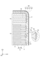
- Fig. 4 is an enlarged view of region R4 in Fig. 3.
- the external electrode 5 has a laminated structure consisting of a first metal layer 23 and a second metal layer 25.
- the first metal layer 23 is in close contact with (or directly overlaps with) the outer surface (e.g., side surface) of the main body portion 3.
- the second metal layer 25 is overlapped on the side surface of the main body portion 3 from above the first metal layer 23. From another perspective, the second metal layer 25 is in close contact with the outer surface of the first metal layer 23.
- FIG. 5 is a view of part of the portion shown in FIG. 4, seen from the +D1 side.
- FIG. 5 is a view of the external electrode 5 located on both the +D1 and +D2 sides and its surroundings, seen in the direction indicated by arrow a1 in FIG. 1.
- the second metal layer 25 is omitted from FIG. 5.
- the internal electrode 9 more specifically, the partial edge 9c of the lead-out electrode 9b
- dummy electrode 19 which are covered by the external electrode 5 and cannot be seen, are shown by dotted lines.
- FIG. 4 is a cross-sectional view taken along line IV-IV in FIG. 5.
- the first metal layer 23 does not extend continuously (in other words, without gaps) across the area where the external electrode 5 is disposed, but extends discontinuously.
- a non-disposition area A1 of the first metal layer 23 is formed on the side of the main body portion 3.
- the non-disposition area A1 is mainly located on the side of the effective portion 13.
- the second metal layer 25 is in close contact with the side of the main body portion 3, not with the first metal layer 23.
- FIG. 6 is an enlarged view of region R6 in FIG. 4.
- the outer surface of the first metal layer 23 (the surface opposite to the main body portion 3) is oxidized.
- the first metal layer 23 has a first material layer 23a and a first oxide layer 23b that covers the first material layer 23a.
- the material of the first oxide layer 23b is an oxide of the material that constitutes the first material layer 23a.
- the outer surface of the second metal layer 25 is oxidized.
- the second metal layer 25 has a second material layer 25a and a second oxide layer 25b that covers the second material layer 25a.
- the material of the second oxide layer 25b is an oxide of the material that constitutes the second material layer 25a.
- the non-disposition area A1 of the first metal layer 23 is mainly located on the side of the effective portion 13 among the side surfaces of the main body portion 3. Therefore, the area ratio of the first oxide layer 23b on the side surface of the effective portion 13 is smaller than the area ratio of the first oxide layer 23b on the side surface of the cover 15. As a result, in the external electrode 5, the volume ratio of the oxide phase in the first portion 5a is smaller than the volume ratio of the oxide phase in the second portion 5b.
- the volume ratio of the oxide phase in the first portion 5a is the ratio of the volume of the oxide phase present in the first portion 5a to the volume of the external electrode 5 present in the first portion 5a
- the volume ratio of the oxide phase in the second portion 5b is the ratio of the volume of the oxide phase present in the second portion 5b to the volume of the external electrode 5 present in the second portion 5b.
- the area ratio of the first oxide layer 23b on the side of the effective portion 13 is the ratio of the area of the first oxide layer 23b present in the first portion 5a to the area of the first portion 5a
- the area ratio of the first oxide layer 23b on the side of the cover 15 is the ratio of the area of the first oxide layer 23b present in the second portion 5b to the area of the second portion 5b.
- the first material layer 23a and the first oxide layer 23b are clearly distinguished, but the boundary between the two does not have to be clear.
- the first material layer 23a may contain an oxide phase
- the first oxide layer 23b may contain a phase that is not an oxide phase.
- the second material layer 25a and the second oxide layer 25b may contain a phase that is not an oxide phase.
- the volume fraction of the oxide phase in the first portion 5a is reduced by making the first metal layer 23 discontinuous on the side surface of the effective portion 13.
- the volume fraction of the oxide phase in the first portion 5a can be easily reduced while making the external electrode 5 a laminated structure.
- the external electrode 5 a laminated structure for example, it is possible to deal with differences between the inner side and the outer side in terms of the functions required of the external electrode 5.
- the first metal layer 23 may have a high adhesion strength to the internal electrode 9 and/or the dielectric layer 7.
- the second metal layer 25 may be made to have a thickness that is easy to ensure in terms of time and/or cost. Examples of the effects of reducing the volume fraction of the oxide phase in the first portion 5a have already been described.
- the first metal layer 23 discontinuous in the active portion 13 and/or the cover 15 effects from a different perspective than those described above can be achieved.
- the surface area of the first metal layer 23 becomes relatively large compared to the volume of the first metal layer 23. Therefore, for example, the affinity between the first metal layer 23 and the second metal layer 25 can be improved while reducing the volume of the first metal layer 23.
- the unevenness caused by the discontinuous first metal layer 23 provides an anchor effect. For these reasons, for example, the thickness of the external electrode 5 can be secured by the relatively inexpensive second metal layer 25, while the adhesive strength of the external electrode 5 to the main body portion 3 can be improved.
- volume fraction of the oxide phase in the first portion 5a is smaller than the volume fraction of the oxide phase in the second portion 5b is met may be determined by an appropriate method. For example, in a mode in which the thickness of the first oxide layer 23b and the thickness of the second oxide layer 25b can be essentially regarded as being roughly constant, the volume fraction is determined by the area of the first oxide layer 23b (i.e., the surface area of the first metal layer 23). Therefore, by comparing the area fraction of the first metal layer 23 between the first portion 5a and the second portion 5b, it may be determined whether or not the above requirement is met.
- the area ratio of the first metal layer 23 in the first portion 5a is the ratio of the area of the first metal layer 23 present in the first portion 5a to the area of the first portion 5a
- the area ratio of the first metal layer 23b in the second portion 5b is the ratio of the area of the first metal layer 23 present in the second portion 5b to the area of the second portion 5b.
- the area ratio of the first metal layer 23 in the first portion 5a is somewhat smaller than the area ratio of the first metal layer 23 in the second portion 5b, it may be determined that the above requirement is met. However, taking into account measurement errors and the like, it may also be determined that the above requirement is met when the area ratio of the former is 0.95 or less, 0.90 or less, or 0.80 or less than the area ratio of the latter.
- the area ratio may be determined based on the manufacturing process, or by analyzing the external electrode 5 after manufacturing. In the latter case, the area ratio may be determined, for example, by imaging and analyzing a mirror surface obtained by polishing the surface or cross section of the external electrode 5.
- the volume ratio of the oxide phase may be determined based on the manufacturing process, or by analyzing the external electrode 5 after manufacturing. In the latter case, for example, an appropriate analytical device that performs qualitative and quantitative analysis of the material may be used. Measurements using an analytical device may be either physical or chemical, and may be destructive or non-destructive. Measurements may be performed on the entire amount of each part (5a and 5b), or on multiple extracted parts of each part.
- the volume ratio of the oxide phase in both portions may be compared by excluding the unclear portion to the minimum necessary size.
- the specific pattern for making the first metal layer 23 discontinuous is arbitrary.
- the first metal layer 23 has a plurality of extending portions 23e extending along the D2 direction (a direction intersecting the stacking direction of the dielectric layers 7 and the internal electrodes 9) in the effective portion 13.
- the positions of the plurality of extending portions 23e in the D3 direction are different from each other.
- the plurality of extending portions 23e are separated from each other in the D3 direction.
- the first metal layer 23 is discontinuous in the D3 direction.
- At least one of the multiple extension portions 23e (all of them in the example of FIG. 5) has a break A3 midway in the D2 direction.
- the extension portion 23e has multiple separation portions 23f that are spaced apart from each other in the D2 direction.
- the first metal layer 23 has multiple separation portions 23f that are distributed apart from each other in the D2 and D3 directions.
- the first metal layer 23 is discontinuous not only in the D3 direction, but also in the D2 direction.
- the portion of the first metal layer 23 that is a single unit may be single crystal or polycrystalline.
- separation portion 23f may be a crystal that has grown in an island shape.
- the island-shaped crystal may be even smaller than separation portion 23f in the illustrated example, and may not fit the concept of a portion obtained by dividing extension portion 23e in the length direction.
- the grain size of the island-shaped crystal in other words, crystal grain
- separation portion 23f is polycrystalline without any particular mention.
- the extensions 23e and multiple separations 23f are arbitrary.
- the extensions 23e extend along the partial edge 9c (the edge exposed from the effective portion 13) of the internal electrode 9 while covering the partial edge 9c.
- the partial edge 9c has a non-exposed portion 9d (symbol in FIG. 4) that is not exposed from the side of the effective portion 13.
- the discontinuity A3 of the extensions 23e overlaps with the non-exposed portion 9d when viewed in the D1 direction (the normal direction of the first portion 5a).
- the shape of the extension portion 23e and the shape of the separation portion 23f are formed in an elongated shape extending with a generally constant width (length in the D3 direction). Unlike the example shown, the shape of the separation portion 23f (or the extension portion 23e) may be an ellipse with the D2 direction as the longitudinal direction. Furthermore, the shape of the separation portion 23f may be a shape that does not allow the concept of a longitudinal direction (for example, a circular shape), or a shape with the D3 direction as the longitudinal direction.
- the extension portion 23e (or the separation portion 23f) extends in the D2 direction, it is sufficient that the maximum length in the D2 direction is somewhat longer than the maximum length in the D3 direction.
- the former may be more than twice or more than five times the latter.
- the multiple extensions 23e do not have to be completely separated from each other.
- the extensions 23e or the separations 23f
- the wide portions of adjacent extensions 23e may be connected to each other.
- the number of interruptions A3 in one extension portion 23e is arbitrary, and may be one (as in the illustrated example) or two or more.
- the length of the interruptions A3 in the D2 direction is also arbitrary.
- the total length of one or more interruptions A3 may be shorter than the total length of the uninterrupted portions of the extension portion 23e.
- one external electrode 5 overlaps two side surfaces of the effective portion 13, and is fixed to the partial edge portion 9c of the internal electrode 9 at the two side surfaces.
- Two extension portions 23e connected to the same internal electrode 9 and located on two side surfaces may be connected to each other (see the first, third, and fifth extension portions 23e from the top in Figure 5), or may not be connected to each other (see the other extension portions 23e in Figure 5).
- More specific settings of the number and width of the extensions 23e and the number and length of the interruptions A3 may be made, for example, so as to realize an example of the coverage value of the first metal layer 23 described in the embodiment described later.
- the ratio of the area of the side surface of the effective portion 13 covered by the first portion 5a (first region) to the area of the first region covered by the first metal layer 23 may be, for example, 50% or more and 95% or less.
- the number and width of the extensions 23e and the number and length of the interruptions A3 may be set so as to realize this area ratio.
- the thickness of the first metal layer 23 and the second metal layer 25 is arbitrary.
- the thickness of the first metal layer 23 e.g., the maximum thickness; the same applies below in this paragraph
- the thickness of the second metal layer 25 e.g., the minimum thickness on the first metal layer 23; the same applies below in this paragraph
- the second metal layer 25 may be thicker than the first metal layer 23.
- the thickness of the second metal layer 25 may be 1.5 times or more or 10 times or more than the thickness of the first metal layer 23.
- the material of the first metal layer 23 and the second metal layer 25 is arbitrary.
- the material of the first material layer 23a and the second material layer 25a or its main component may be a base metal.
- the base metal may be, for example, Cu, Ni, or an alloy containing at least one of Cu and Ni (for example, a Cu-Ni alloy).
- the main component may be, for example, a component that occupies 60 mass% or more or 80 mass% or more of the material (the same applies to layers other than the first metal layer 23 and the second metal layer 25).
- the material is Cu, Ni, or a Cu-Ni alloy, unintended impurities may be present.
- the impurities may be, for example, less than 1 mass% of the material.
- the material of the first oxide layer 23b and the second oxide layer 25b or its main component may be an oxide of the material exemplified above.
- the oxide may be Cu 2 O, CuO, NiO, or Ni 2 O 3 .
- the materials or main components of the first metal layer 23 and the second metal layer 25 may be the same or different.
- the difference between the materials may be, for example, based only on the elemental component ratio, or based on the grain size of the crystal grains in addition to the elemental component ratio (this also applies to layers other than the first metal layer 23 and the second metal layer 25). Even if the elements and grain size of the first metal layer 23 and the second metal layer 25 are the same, in the configuration illustrated in FIG. 6, the existence of the first metal layer 23 and the second metal layer 25 can be confirmed by the first oxide layer 23b.
- the material or main component of at least one of the first metal layer 23 and the second metal layer 25 may be the same as the material or main component of the internal electrode 9, or may be different.
- FIG. 7 is an enlarged view of region R7 in FIG. 6.
- crystal grains are depicted for the first metal layer 23 and the second metal layer 25. However, whether or not they are oxide phases is omitted. Also, crystal grains are omitted for areas other than the first metal layer 23 and the second metal layer 25.
- the first metal layer 23 and the second metal layer 25 are, for example, made of polycrystalline bodies. That is, the first metal layer 23 has a plurality of first crystal grains 23p, and the second metal layer 25 has a plurality of second crystal grains 25p.
- the grain size of the two may be larger than that of the other (as shown in the example) or may be the same. In the example shown, the grain size of the first crystal grains 23p is smaller than the grain size of the second crystal grains 25p.
- the particle size referred to here may be, for example, the circle equivalent diameter in the cross section (or, from another point of view, the two-dimensional image) of the metal layers (23 and 25).
- the particle sizes compared in the first metal layer 23 and the second metal layer 25 may be average particle sizes unless otherwise specified.
- the average particle size may be, for example, the particle size at which the area ratio is 50% when the areas of the smallest particle sizes are integrated in the above two-dimensional image. In other words, the average particle size may be the average value based on the area.
- the particle sizes of the first metal layer 23 and the second metal layer 25 may not distinguish whether they are oxide phases or not.
- the specific values of the grain size of the first crystal grains 23p and the grain size of the second crystal grains 25p and the difference between them are arbitrary.
- the average grain size of the first crystal grains 23p may be less than 1 ⁇ m, and more specifically, may be 0.1 ⁇ m or more and less than 1 ⁇ m.
- the average grain size of the second crystal grains 25p may be 1 ⁇ m or more, and more specifically, may be 1 ⁇ m or more and less than 10 ⁇ m.
- the average grain size of the second crystal grains 25p may be two or more times or five or more times the average grain size of the first crystal grains 23p.
- the grain size may be measured, for example, by mirror-finishing the surface or cross section of the metal layers (23 and 25), appropriately chemically etching the surface to clarify the grain boundaries, and imaging the mirror surface with an electron microscope. More specifically, for example, the first metal layer 23 is imaged at a scale where the first crystal grains 23p number 30 to 50. The second metal layer 25 is imaged at a scale where the second crystal grains 25p number 30 to 50. The scales of the two may be different. Then, known image processing is performed on the image of each metal layer to calculate the circle equivalent diameter. Multiple images may be imaged until the variation due to the imaging position converges, and the average value of the average grain size may be calculated.
- the presence of the grain size difference can be identified by visual inspection of the image, and the presence of the first metal layer 23 and the second metal layer 25 can be confirmed.
- images of multiple continuous regions are taken while appropriately changing the scale so that 30 to 50 crystal grains are included, and the grain size (circle equivalent diameter) of each crystal grain is measured.
- the change in grain size of crystal grains located on a predetermined straight line spanning multiple regions may be analyzed to confirm the presence of the first metal layer 23 and the second metal layer 25.
- the presence of the first metal layer 23 and the second metal layer 25 can be confirmed when the grain size at the peak (second metal layer 25) is at least two or five times the grain size at the valley (first metal layer 23).
- FIG. 8 is a diagram showing another example of the internal electrode 9 and the external electrode 5, and corresponds to FIG.
- the thickness of the partial edge portion 9c (the portion exposed from the side of the effective portion 13) may be thicker than the portion inside the partial edge portion 9c. From another perspective, the exposed area of the partial edge portion 9c to the outside may be made larger.
- the first metal layer 23 may cover the entire thickness of the partial edge portion 9c. In other words, the bonding area between the partial edge portion 9c and the first metal layer 23 may be expanded in the thickness direction (direction D3) of the internal electrode 9 compared to the embodiment in FIG. 4.
- the partial edge portion 9c that is thickened as described above may be referred to as the expanded edge portion 9e.
- edges constituting the partial edge 9c only two types of edges are shown as edges constituting the partial edge 9c: the extended edge 9e and the non-exposed portion 9d described above.
- these three types of edges, and an edge having the same thickness as the thickness of the inner portion of the internal electrode 9 may be provided as appropriate.
- the normal edge 9f and the extended edge 9e there are an embodiment in which the above three types of edges are provided, an embodiment in which the normal edge 9f and the extended edge 9e are provided, an embodiment in which only the normal edge 9f is provided, and an embodiment in which only the extended edge 9e is provided.
- the two may be provided on different partial edges 9c, or on the same partial edge 9c.
- the specific shape and dimensions of the extended edge 9e are arbitrary.
- the extended edge 9e is shaped to gradually become thicker by equal amounts on both the top and bottom sides as it moves outward (toward the external electrode 5).
- Other examples of shapes include a shape that is thicker only upward or downward, a shape that is thicker on both the top and bottom sides but the amount of thickening on one side is greater than the amount of thickening on the other side, and a shape that is not gradually thicker but thickens so that a step is created and/or the edge of the internal electrode 9 is bent.
- the thickness (e.g., maximum thickness) of the extended edge 9e may be, for example, 1.2 times or more, 1.5 times or more, or 2 times or more the thickness of the inner part of the internal electrode 9.
- the external electrode 5A shown in FIG. 8 is obtained by adding a third metal layer 27 and a fourth metal layer 29 to the external electrode 5 shown in FIG. 4.
- the third metal layer 27 and the fourth metal layer 29 contribute, for example, to reducing the solder erosion of the second metal layer 25, reducing the oxidation of the second metal layer 25, and/or improving the bonding strength to a bonding material (e.g., solder).
- Only one of the third metal layer 27 and the fourth metal layer 29 may be provided, or another metal layer may be provided.
- the material and thickness of the third metal layer 27 and the fourth metal layer 29 may be appropriately set according to the purpose of these layers.
- the third metal layer 27 may be Ni
- the fourth metal layer 29 may be Sn.
- the external electrode 5A is combined with an internal electrode 9 having an extended edge portion 9e and a non-exposed portion 9d.
- the external electrode 5A may be combined with an internal electrode 9 that does not have an extended edge portion 9e and/or a non-exposed portion 9d.
- FIG. 9 is a diagram showing another example of the pattern of the first metal layer 23 and corresponds to FIG.
- the extension 23e does not have a gap A3.
- the first metal layer 23 is discontinuous in the D3 direction (stacking direction) but is continuous in the D2 direction (direction intersecting the stacking direction).
- the partial edge 9c of the internal electrode 9 does not have a non-exposed portion 9d.
- the partial edge 9c shown in FIG. 9 may be a normal edge 9f (FIG. 4) or an extended edge 9e (FIG. 8), or a combination of these. Also, depending on the method of forming the pattern of the first metal layer 23 (described later), the first metal layer 23 in the pattern shown in FIG. 9 may be combined with a non-exposed portion 9d.
- the capacitor 1 may be manufactured by various methods.
- the outline of the manufacturing process may be the same as a known process. An example is shown below.
- ceramic green sheets that will become the dielectric layer 7 and insulating layer 17 are prepared.
- a conductive paste that will become the internal electrode 9 or dummy electrode 19 is applied (e.g., printed) to the ceramic green sheets.
- the ceramic green sheets are stacked to prepare a laminate that will become the main body portion 3. Note that the stacking of the laminate that will become the active portion 13 and the stacking of the portion that will become the cover 15 for the laminate may be performed together or separately.
- the above-mentioned process up to the creation of the laminate is carried out, for example, on a mother board the size of which a large number of main body parts 3 are to be cut.
- the mother board including the laminate is diced (e.g. cut) into pieces of a size roughly corresponding to the size of the main body parts 3.
- the laminate having the size of the main body parts 3 is fired. After that, a metal film is formed on the main body parts 3, and the external electrodes 5 are formed.
- Degreasing may be performed before firing. Firing may be performed, for example, in a reducing atmosphere. Reoxidation heat treatment may be performed after firing. Polishing (e.g., barrel polishing) of the main body portion 3 may be performed before and/or after firing. In polishing, for example, the ridges of the main body portion 3 may be chamfered or the side surfaces of the main body portion 3 may be polished. By polishing, the partial edge portion 9c of the internal electrode 9 and the edge portion of the dummy electrode 19 may be exposed from the side surface of the main body portion 3.
- Polishing e.g., barrel polishing
- Metal may be deposited by electroless plating or electrolytic plating on the surfaces of the internal electrodes 9 and dummy electrodes 19 that are exposed to the outside of the main body 3 (hereinafter sometimes referred to as "exposed surfaces"), thereby forming the first metal layer 23.
- the pattern of the first metal layer 23 will have a shape based on the patterns of the exposed surfaces of the internal electrodes 9 and dummy electrodes 19. Therefore, by giving the patterns of the exposed surfaces of the internal electrodes 9 and dummy electrodes 19 an appropriate shape and ensuring that the metal deposited on the exposed surfaces is not connected via non-placement areas of the exposed surfaces, the first metal layer 23 can be formed into any pattern.
- the gaps between the exposed surfaces of the multiple dummy electrodes 19 are made smaller than the gaps between the exposed surfaces of the multiple internal electrodes 9. Then, the plating conditions (e.g., deposition time) are adjusted so that the deposited metal connects between the exposed surfaces of the multiple dummy electrodes 19, but does not connect between the exposed surfaces of the multiple internal electrodes 9. This forms a first metal layer 23 having multiple extensions 23e.
- the plating conditions e.g., deposition time
- the non-exposed portion 9d already described is provided on the partial edge portion 9c of the internal electrode 9. That is, the exposed surface of the internal electrode 9 is interrupted halfway. Then, the plating conditions (e.g., deposition time) are adjusted so that the metal deposited on the exposed surface of the internal electrode 9 does not continue beyond the interruption of the exposed surface. This forms an extension portion 23e having an interruption A3.
- the non-exposed portion 9d is provided in a position where adjacent extension portions 23e are likely to be connected to each other, the non-exposed portion 9d also makes it difficult for multiple extension portions 23e to be connected to each other.
- the first metal layer 23 may be formed through a mask, or the first metal layer 23 may be formed and then etched through a mask. Etching may be performed, for example, by laser processing or blasting. As can be understood from this, the first metal layer 23 does not necessarily have to cover the exposed surface (partial edge portion 9c) of the internal electrode 9, and does not necessarily have to have a pattern corresponding to the pattern of the exposed surface of the internal electrode 9.
- the first metal layer 23 may also be formed by a method other than electroless plating and electrolytic plating (for example, sputtering).
- the first metal layer 23 is formed by electroless plating or electrolytic plating, either may be used.
- the first metal layer 23 may be formed by electroless plating.
- the second metal layer 25 may be formed by electrolytic plating. By doing so, for example, it is possible to ensure the thickness of the second metal layer 25 in a short time and/or at low cost while improving the bonding strength between the internal electrode 9 and the first metal layer 23.
- the non-exposed portion 9d may be formed by a pattern when the conductive paste that will become the internal electrode 9 is printed on a ceramic green sheet. That is, in a plan view of the internal electrode 9, the non-exposed portion 9d may be formed by making the shape of the partial edge portion 9c have a portion that is separated from the edge of the dielectric layer 7, rather than making it a straight line parallel to the edge of the dielectric layer 7.
- the side of the effective portion 13 may be partially removed after (or before) firing to partially expose the partial edge portion 9c. That is, the portion of the partial edge portion 9c located in the region of the side of the effective portion 13 that has not been removed may be the non-exposed portion 9d.
- the removal may be performed, for example, by blasting or laser processing, or a mask may be used.
- barrel polishing may be performed before and/or after firing.
- the chip (main body 3) is housed in a barrel, and polishing is performed by rotating the barrel, etc. Therefore, the ridges of the main body 3 are easily chamfered, and the dummy electrode 19 is more likely to be exposed on the outer surface of the main body 3 than the internal electrode 9.
- the first metal layer 23 is formed by depositing metal on the exposed surfaces of the internal electrode 9 and the dummy electrode 19, the first metal layer 23 is more likely to spread continuously on the dummy electrode 19 than on the internal electrode 9.
- the method of forming the extended edge portion 9e ( Figure 8) of the internal electrode 9 is also arbitrary.
- the extended edge portion 9e may be formed by stretching and deforming the internal electrode 9 by a blasting process after (or before) firing.
- the blasting process may also serve as a process for partially removing the side surface of the above-mentioned effective portion 13.
- the extended edge portion 9e may also be formed by thickening only the portion that will become the extended edge portion 9e when applying the conductive paste that will become the internal electrode 9.
- the material of the powder projected and the direction in which the powder is projected are arbitrary.
- the projection direction may be tilted in the D3 direction with respect to the normal to the side of the effective portion 13. In this case, for example, it is easier to extend and deform the edge of the internal electrode 9 in the D3 direction.
- the specific magnitude of the tilt angle is arbitrary.
- a method for making the volume ratio of the oxide phase in the first portion 5a (portion covering the effective portion 13) smaller than the volume ratio of the oxide phase in the second portion 5b (portion covering the cover 15) may be achieved by making the area ratio of the first metal layer 23 in the first portion 5a smaller than the area ratio of the first metal layer 23 in the second portion 5b.
- a method for making the area ratio of the first metal layer 23 in the first portion 5a smaller is achieved by forming the first metal layer 23 into an appropriate pattern.
- the first oxide layer 23b is formed, for example, by exposing the first metal layer 23 to an oxidizing atmosphere after the first metal layer 23 is formed with the material of the first material layer 23a and before the second metal layer 25 is formed. At this time, the thickness of the first oxide layer 23b (or, from another perspective, the volume fraction of the oxide phase in the first metal layer 23) may be adjusted by adjusting the time of exposure to the oxidizing atmosphere, etc. Also, the volume fraction of the oxide phase may be adjusted by using an oxidizing agent or a reducing agent.
- the second oxide layer 25b is formed by forming the second metal layer 25 with the material of the second material layer 25a, and then exposing the second metal layer 25 to an oxidizing atmosphere.
- the thickness of the second oxide layer 25b (or, from another perspective, the volume fraction of the oxide phase in the second metal layer 25) may be adjusted by adjusting the time for which the second metal layer 25 is exposed to the oxidizing atmosphere.
- the volume fraction of the oxide phase may also be adjusted by using an oxidizing agent or a reducing agent.
- the method of making the volume fraction of the oxide phase in the first portion 5a smaller than the volume fraction of the oxide phase in the second portion 5b is not limited to adjusting the area fraction of the first metal layer 23. From another perspective, the first metal layer 23 does not have to extend discontinuously, and may extend without gaps.
- the first metal layer 23 may be formed without gaps over the entire area of the side surface of the main body portion 3 that is to be covered by the external electrode 5. Then, after the first oxide layer 23b is formed, and before the second metal layer 25 is formed, the first oxide layer 23b may be removed from part or all of the side surface of the effective portion 13 in the above-mentioned area using a reducing agent.
- the first portion 5a may be formed after the second portion 5b is formed. Then, after the second portion 5b is formed and before the first portion 5a is formed, a heat treatment may be performed to form an oxide phase in the region of the second portion 5b on the main body portion 3 side. In this case, for example, the oxide phase of the second portion 5b improves the adhesion strength of the second portion 5b to the main body portion 3.
- Fig. 10 is a perspective view of a capacitor 201 according to the second embodiment.
- Fig. 3 according to the first embodiment may be referred to as a cross-sectional view taken along line IIIB-IIIB in Fig. 10.
- reference numerals 1 and 3 in Fig. 3 are replaced with reference numerals 201 and 203.
- the specific dimensions of each part and the like in Fig. 3 do not necessarily coincide with those in Fig. 10.
- capacitor 201 differs from capacitor 1, which is a four-terminal type, in that it is a two-terminal type.
- capacitor 201 has the same basic configuration for functioning as a capacitor as capacitor 1, and is also similar to capacitor 1 in that the volume fraction of the oxide phase in first portion 5a is smaller than the volume fraction of the oxide phase in second portion 5b. More specifically, it is as follows.
- the shape of the main body 203 is, for example, roughly rectangular.
- the height (length in the D3 direction) of this rectangular parallelepiped may be equal to (as in the illustrated example) or smaller than the width (length in the D2 direction).
- the length (D1 direction) of the rectangular parallelepiped is, for example, greater than the width.
- the dimensions of the main body 203 are arbitrary. Examples of relatively small dimensions include a length of 0.4 mm or more and 3.2 mm or less, and a width and height of 0.2 mm or more and 2.5 mm or less.
- the external electrode 5 is roughly layered and covers the longitudinal ends of the main body 203 over the five faces of the rectangular parallelepiped.
- the main body 203 has an active part 13 and a cover 15, as in the first embodiment (see FIG. 3).
- the active part 13 is constructed by alternately stacking dielectric layers 7 and internal electrodes 9.
- the cover 15 has at least one insulating layer 17 and at least one dummy layer 21.
- the dummy layer 21 includes a plurality of dummy electrodes 19.
- the position and shape of the internal electrode 9 in plan view are different from those in the first embodiment.
- the shape of the internal electrode 9 is generally a rectangle having four sides parallel to the four sides of the rectangle of the main body 203 (dielectric layer 7). Of the four sides of the internal electrode 9, two long sides and one short side are located inside the side of the main body 203 (not exposed). The remaining short side is exposed from the side of the +D1 side or -D1 side of the main body 203 and is connected to the external electrode 5 on the +D1 side or -D1 side.
- the internal electrodes 9 connected to different external electrodes 5 are stacked alternately.
- the area of the internal electrode 9 that overlaps with other internal electrodes 9 in plan view is the electrode body 9a.
- the portion extending from the electrode body 9a to the external electrode 5 is the extraction electrode 9b.
- each dummy layer 21 has two dummy electrodes 19 at both ends of the longitudinal direction of the main body portion 203.
- the dummy electrodes 19 are rectangular across the entire width (length in the D2 direction) of the main body portion 203, and are exposed, for example, from the side surface on the +D1 side or -D1 side of the main body portion 203, and also from the side surface on the +D2 side and the -D2 side.
- the requirements regarding the volume ratio of the oxide phase, etc. only need to be met within the range of the length of the partial edge portion 9c of the internal electrode 9 (target portion 5c of the external electrode 5). Therefore, with regard to the above requirements, the portions of the external electrode 5 that cover the top and bottom surfaces, the +D2 side surface, and the -D1 side surface of the main body portion 203 may be ignored. In addition, when focusing on the portion of the external electrode 5 that covers the side surface on the +D1 side (or the -D1 side), the portion that covers the so-called side margin portion from the +D1 side (or the -D1 side) may also be ignored.
- the side margin portion is the portion of the main body portion 203 that extends from the edge portion on the +D2 side (or the -D2 side) of the internal electrode 9 to the side surface on the +D2 side (or the -D2 side) of the main body portion 203.
- the capacitor may have an exterior resin that covers the entire structure illustrated in FIG. 1 or FIG. 10, and a lead wire that is connected to the external electrode 5 and extends from the exterior resin.
- the capacitor may be a through-hole mount type rather than a surface mount type.
- one external electrode 5 may only cover one side surface.
- Two types of internal electrodes 9 connected to different external electrodes 5 may be alternately stacked two at a time, rather than one at a time.
- the thickness of the dielectric layer 7 between the internal electrodes 9 that are connected to the same external electrode 5 and face each other may be thinner than the thickness of the dielectric layer 7 between the internal electrodes 9 that are connected to different external electrodes 5 and face each other.
- the multiple dielectric layers 7 do not have to have the same shape and size.
- the two types of internal electrodes 9 connected to different external electrodes 5 do not have to face each other.
- two types of internal electrodes 9 connected to different external electrodes 5 may be provided in the same layer, and an internal electrode 9 facing the two types of internal electrodes 9 may be provided, thereby forming a circuit in which two parallel plate capacitors are connected in series.
- a circuit in which three or more parallel plate capacitors are connected in series may be formed.
- the side margin portion was mentioned.
- the side margin portion is, for example, formed by a portion of the dielectric layer 7 that extends further toward the +D2 side or the -D2 side than the internal electrode 9.
- the side margin portion may also be formed by overlapping another dielectric layer on the +D2 side or the -D2 side of the laminate formed by the dielectric layer 7. From another point of view, the main body portion 203 does not need to have a laminated structure in its entirety.
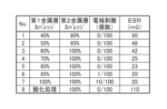
- Examples 11 is a table showing the results of investigating the characteristics of a prototype capacitor according to the embodiment (more specifically, the capacitor 201 according to the second embodiment). This figure shows that, for example, by making the first metal layer 23 discontinuous and reducing the volume ratio of the oxide phase in the first portion 5a, it is possible to improve the adhesion strength and reduce the ESR at the same time. Specifically, this is as follows.
- No. is an identification number assigned to the examples and comparative examples.
- No. 1 to No. 6 are examples, and No. 7 is a comparative example.
- First metal layer coverage indicates the area percentage (%) of the first metal layer 23 in the region of the side of the effective portion 13 where the target portion 5c of the external electrode 5 should overlap (i.e., the region where the first portion 5a should be formed), except for No. 8.
- “Second metal layer coverage” indicates the area percentage of the second metal layer 25 in the above region. Note that, for convenience, in the following, the above area percentage may be referred to simply as the area percentage on the side of the effective portion 13, without mentioning that it is in the region where the target portion 5c should overlap.
- Electrode peeling indicates the number of external electrodes 5 that peeled off in an experiment on 100 samples, expressed as a fraction.
- ESR (m ⁇ ) indicates the measured ESR value.
- the first metal layer 23 and the second metal layer 25 are each formed over the entire area of the side surface of the cover 15 where the target portion 5c of the external electrode 5 should overlap.
- the area ratio of each layer is 100%, and from another perspective, the area ratios of the two layers are the same.
- the area ratio of the first metal layer 23 on the side surface of the effective portion 13 is less than 100% (specifically, 40% or more and 95% or less). Also, the area ratio of the second metal layer 25 on the side surface of the effective portion 13 is 80% or more and 100% or less. From another perspective, in the first portion 5a, the area ratio of the first metal layer 23 is smaller than the area ratio of the second metal layer 25.
- the area proportions of the first metal layer 23 and the second metal layer 25 are the same, so in the examples (No. 1 to No. 6) in which the area proportion of the first metal layer 23 in the first portion 5a is smaller than the area proportion of the second metal layer 25, the volume proportion of the oxide phase in the first portion 5a is smaller than the volume proportion of the oxide phase in the second portion 5b.
- the area ratio of each of the first metal layer 23 and the second metal layer 25 on the side surface of the effective portion 13 is 100%. From another perspective, in the first portion 5a, as in the second portion 5b, the area ratios of the two layers are the same. Therefore, the volume ratio of the oxide phase in the first portion 5a is the same as the volume ratio of the oxide phase in the second portion 5b.
- the first metal layer 23 is formed over a relatively wide area of the side surface of the effective portion 13, and the volume fraction of the oxide phase is increased by performing an oxidation treatment (a treatment not performed in Nos. 1 to 7) on the first metal layer 23.
- an oxidation treatment a treatment not performed in Nos. 1 to 7
- the volume fraction of the oxide phase in the first portion 5a and the second portion 5b is larger than in the other examples (Nos. 1 to 7).
- the first metal layer 23 is formed by electroless plating
- the second metal layer 25 is formed by electroless plating.
- the second metal layers 25 are intended to be the same thickness.
- the area ratio of the second metal layer 25 does not reach 100% due to the small area ratio of the first metal layer 23.
- the specifications of the capacitor 201 used in the experiment are as follows: Length in D1 direction: 1.0 mm Length in the D2 and D3 directions: 0.5 mm Thickness of cover 15 (D3 direction): 30 ⁇ m ⁇ Width of side margin (D2 direction): 30 ⁇ m Thickness of dielectric layer 7: 1.0 ⁇ m Number of layers of internal electrodes 9: 20 layers
- the number of cases where electrode peeling occurred was 0/100 when the coverage of the first metal layer 23 was 40% or more and 80% or less (No. 1 to No. 5), and 1/100 when it was 95% (No. 6). In contrast, when the coverage of the first metal layer 23 became 100%, the number of cases where electrode peeling occurred increased sharply (10/100). Therefore, it can be said that the effect of reducing electrode peeling is easily achieved when the coverage of the first metal layer 23 is 40% or more and 95% or less (or 40% or more and 80% or less).
- a non-exposed portion 9d that is not exposed from the side of the main body portion 203 is provided at the partial edge portion 9c of the internal electrode 9 to prevent the first metal layer 23 from precipitating, thereby reducing the area ratio of the first metal layer 23 and thus reducing the volume ratio of the oxide phase (first oxide layer 23b). Therefore, when the coverage of the first metal layer 23 is reduced, the volume ratio of the oxide phase with high electrical resistivity is reduced, but the cross-sectional area of the connection between the internal electrode 9 and the external electrode 5 is reduced. As a result, the smaller the coverage of the first metal layer 23, the higher the ESR.
- the ESR is reduced compared to when oxidation treatment is performed.
- the adhesion strength of the external electrode 5 to the main body portion 203 is improved by the oxidation treatment, and the number of external electrodes 5 that peeled off is 0/100. Therefore, it can be said that by reducing the area ratio of the first metal layer 23 in the effective portion 13, it is possible to improve the adhesion strength without performing oxidation treatment, thereby achieving both improved adhesion strength and reduced ESR.
- An example of the range of coverage of the first metal layer 23 is 40% or more and 95% or less, which is the range in the embodiment. Also, from the viewpoint of the range in which no peeling occurs at all, 40% or more and 80% or less can be mentioned. Since the ESR roughly doubles when the coverage of the first metal layer 23 changes from 50% to 40%, from this viewpoint, 50% or more and 95% or less can be mentioned. As an overlapping portion of the previous two viewpoints, 50% or more and 80% or less can be mentioned.
- FIG. 11 is based on the capacitor 201 according to the second embodiment, and is based on a sample of the capacitor 201 having specific specifications. However, it is clear that within the above range, a better effect can be obtained, even if it is not the best effect.
- the capacitor 1 (or 201) has an effective portion 13, a cover 15, and an external electrode 5.
- the effective portion 13 has dielectric layers 7 and internal electrodes 9 that are alternately stacked.
- the cover 15 overlaps the effective portion 13 in the stacking direction (D3 direction) of the dielectric layers 7 and the internal electrodes 9.
- the external electrode 5 covers the side surfaces of the effective portion 13 and the cover 15 along the D3 direction, and is connected to a partial edge portion 9c that is a part of the outer edge of the internal electrode 9.
- the portion covering the side surface of the effective portion 13 is referred to as a first portion 5a
- the portion covering the side surface of the cover 15 is referred to as a second portion 5b.
- the volume ratio of the oxide phase in the first portion 5a is smaller than the volume ratio of the oxide phase in the second portion 5b.
- the external electrode 5 may have a first metal layer 23 and a second metal layer 25.
- the first metal layer 23 may be in close contact with the side of the active portion 13 and the side of the cover 15.
- the second metal layer 25 may overlap the first metal layer 23 with the side of the active portion 13 and the side of the cover 15.
- the first metal layer 23 may extend discontinuously. This may form a non-disposition area A1 of the first metal layer 23.
- the second metal layer 25 may be in close contact with the side of the active portion 13 in the non-disposition area A1.
- the first oxide layer 23b is formed on the surface of the first metal layer 23, so by making the first metal layer 23 discontinuous on the side surface of the effective portion 13, the volume ratio of the oxide phase in the first portion 5a can be reduced.
- This provides the above-mentioned effect of reducing ESR, etc.
- the adhesion strength between the first metal layer 23 and the second metal layer 25 can be improved. As shown with reference to the examples, it is easy to achieve both a reduction in ESR and an improvement in adhesion strength.
- the first metal layer 23 and the second metal layer 25 may each be composed of a polycrystalline body.
- the average grain size of the first crystal grains 23p in the first metal layer 23 may be smaller than the average grain size of the second crystal grains 25p in the second metal layer 25.
- the surface area of the first metal layer 23 is likely to be large compared to, for example, an embodiment in which the average grain size of the first crystal grains 23p is relatively large (such an embodiment is also included in the technology related to the present disclosure).
- the affinity between the first metal layer 23 and the second metal layer 25 is improved, and the bonding strength between the two is likely to be improved.
- the average grain size of the second crystal grains 25p is relatively large, the number of grain boundaries can be reduced. As a result, for example, the probability of moisture penetrating from the outside can be reduced.
- the ratio of the area of the side surface of the effective portion 13 that is covered by the first metal layer 23 to the area of the first region that is covered by the first portion 5a may be 50% or more and 95% or less.
- the first metal layer 23 may have multiple extension portions 23e that extend in a direction intersecting the stacking direction (direction D3) (direction D2 in FIG. 5) at different positions in the stacking direction (direction D3).
- the separation portion 23f may also be considered as a type of extension portion.
- the first metal layer 23 and the second metal layer 25 engage in the stacking direction, making it easier to improve the bonding strength between them in the D3 direction.
- the capacitor 1 (201) often faces the circuit board on which the capacitor 1 is mounted in the D3 direction, and as a result, there is a high probability that the capacitor 1 will be peeled off from the circuit board in the D3 direction. Therefore, by improving the bonding strength in the D3 direction, it becomes easier to efficiently improve the strength of the external electrode 5.
- At least one of the multiple extensions 23e may have a break A3 midway in the intersecting direction (direction D2 in FIG. 5).
- the first metal layer 23 and the second metal layer 25 engage in two directions: the D3 direction and a direction intersecting the D3 direction. As a result, it is easy to improve the bonding strength in various directions.
- the multiple extensions 23e may extend along the partial edge portions 9c so as to cover the partial edge portions 9c of the multiple internal electrodes 9.
- the extension portion 23e can be formed by forming the first metal layer 23 on the partial edge portion 9c by electroless plating or electrolytic plating. In other words, the first metal layer 23 can be easily made discontinuous.
- the partial edge portion 9c may have a non-exposed portion 9d (FIG. 4) that is not exposed from the side of the effective portion 13 midway in the intersecting direction (direction D2 in FIG. 5).
- the extension portion 23e that covers the partial edge portion 9c that has the non-exposed portion 9d may have an interruption A3 at a position that overlaps with the non-exposed portion 9d.
- the extension portion 23e having the discontinuity A3 can be formed by depositing the first metal layer 23 on the partial edge portion 9c by electroless plating or electrolytic plating. In other words, it is easy to make the extension portion 23e discontinuous in its extension direction.
- the thickness of the partial edge portion 9c may be thicker than the portion of the internal electrode 9 that is more inward than the partial edge portion 9c.
- the adhesion area between the external electrode 5 (e.g., the first metal layer 23) and the partial edge portion 9c is increased, and therefore the adhesion strength between the two can be improved.
- the internal electrode 9 can be stretched and deformed to thicken the partial edge portion 9c while performing the process for exposing it, thereby reducing the likelihood of an increase in the number of processes.
- the effective portion 13 may have a rectangular shape when viewed in the stacking direction (D3 direction).
- the cover 15 may have four dummy electrodes 19 and an insulating layer 17.
- the four dummy electrodes 19 may be located at the four corners of the effective portion 13 when viewed in the D3 direction.
- the insulating layer 17 may cover the four dummy electrodes 19 from the side opposite the effective portion 13.
- the four external electrodes 5 may be fixed to the four dummy electrodes 19.
- the strength of adhesion of the external electrode 5 to the main body 3 can be improved.
- the first metal layer 23 by electroless plating or electrolytic plating, by depositing metal on the dummy electrode 19, it becomes easier to form the first metal layer 23 without gaps on the side of the cover 15. Since the dummy electrode 19 is located on the diagonal line of the rectangular main body 3, which makes it easy to ensure the length, the dummy electrode 19 can be easily separated from the electrode main body 9a. This in turn makes it easier to reduce the effect of the dummy electrode 19 on the characteristics of the effective portion 13.
- the multilayer electronic component is not limited to a capacitor.
- some of the internal electrodes may form a capacitor, and other parts of the internal electrodes may form an inductor or resistor.
- the multilayer electronic component may form an appropriate circuit (for example, a resonant circuit) as a whole.
- it is sufficient that at least a portion of the multilayer electronic component is formed by laminating dielectric layers and internal electrodes, and it is not necessary that all or most of the multilayer electronic component is formed from a laminate.
- a concept may be extracted that does not require that the volume fraction of the oxide phase in the first portion 5a be smaller than the volume fraction of the oxide phase in the second portion 5b.
- a concept may be extracted that is characterized in that the first metal layer 23 extends discontinuously, or a concept may be extracted that is characterized in that the partial edge portion 9c of the internal electrode 9 is thicker than the inner portion of the internal electrode 9.
Landscapes
- Engineering & Computer Science (AREA)
- Power Engineering (AREA)
- Manufacturing & Machinery (AREA)
- Microelectronics & Electronic Packaging (AREA)
- Fixed Capacitors And Capacitor Manufacturing Machines (AREA)
- Ceramic Capacitors (AREA)
Priority Applications (2)
| Application Number | Priority Date | Filing Date | Title |
|---|---|---|---|
| JP2024558232A JP7646100B1 (ja) | 2023-07-25 | 2024-07-02 | 積層型電子部品 |
| JP2025033611A JP7678950B1 (ja) | 2023-07-25 | 2025-03-04 | 積層型電子部品 |
Applications Claiming Priority (2)
| Application Number | Priority Date | Filing Date | Title |
|---|---|---|---|
| JP2023120612 | 2023-07-25 | ||
| JP2023-120612 | 2023-07-25 |
Publications (1)
| Publication Number | Publication Date |
|---|---|
| WO2025022942A1 true WO2025022942A1 (ja) | 2025-01-30 |
Family
ID=94374815
Family Applications (1)
| Application Number | Title | Priority Date | Filing Date |
|---|---|---|---|
| PCT/JP2024/023863 Pending WO2025022942A1 (ja) | 2023-07-25 | 2024-07-02 | 積層型電子部品 |
Country Status (2)
| Country | Link |
|---|---|
| JP (2) | JP7646100B1 (https=) |
| WO (1) | WO2025022942A1 (https=) |
Citations (6)
| Publication number | Priority date | Publication date | Assignee | Title |
|---|---|---|---|---|
| JPH05335175A (ja) * | 1992-05-28 | 1993-12-17 | Nec Corp | 積層セラミックコンデンサ |
| JP2007073883A (ja) * | 2005-09-09 | 2007-03-22 | Rohm Co Ltd | チップ型コンデンサ |
| JP2010034503A (ja) * | 2008-06-25 | 2010-02-12 | Murata Mfg Co Ltd | 積層セラミック電子部品およびその製造方法 |
| WO2010137379A1 (ja) * | 2009-05-26 | 2010-12-02 | 株式会社村田製作所 | 3端子コンデンサ及び3端子コンデンサ実装構造 |
| JP2012142478A (ja) * | 2011-01-05 | 2012-07-26 | Murata Mfg Co Ltd | 積層型電子部品およびその製造方法 |
| JP2015023120A (ja) * | 2013-07-18 | 2015-02-02 | Tdk株式会社 | 積層コンデンサ |
Family Cites Families (6)
| Publication number | Priority date | Publication date | Assignee | Title |
|---|---|---|---|---|
| JP2000306763A (ja) | 1999-04-19 | 2000-11-02 | Matsushita Electric Ind Co Ltd | 積層セラミックコンデンサとその製造方法 |
| JP2006147901A (ja) * | 2004-11-22 | 2006-06-08 | Murata Mfg Co Ltd | 積層電子部品、その製造方法およびその特性測定方法 |
| JP2006237078A (ja) * | 2005-02-22 | 2006-09-07 | Kyocera Corp | 積層電子部品及び積層セラミックコンデンサ |
| JP5217677B2 (ja) * | 2008-06-20 | 2013-06-19 | 株式会社村田製作所 | 積層セラミック電子部品およびその製造方法 |
| KR101933416B1 (ko) | 2016-12-22 | 2019-04-05 | 삼성전기 주식회사 | 커패시터 부품 |
| KR102333094B1 (ko) * | 2019-07-08 | 2021-12-01 | 삼성전기주식회사 | 커패시터 부품 |
-
2024
- 2024-07-02 WO PCT/JP2024/023863 patent/WO2025022942A1/ja active Pending
- 2024-07-02 JP JP2024558232A patent/JP7646100B1/ja active Active
-
2025
- 2025-03-04 JP JP2025033611A patent/JP7678950B1/ja active Active
Patent Citations (6)
| Publication number | Priority date | Publication date | Assignee | Title |
|---|---|---|---|---|
| JPH05335175A (ja) * | 1992-05-28 | 1993-12-17 | Nec Corp | 積層セラミックコンデンサ |
| JP2007073883A (ja) * | 2005-09-09 | 2007-03-22 | Rohm Co Ltd | チップ型コンデンサ |
| JP2010034503A (ja) * | 2008-06-25 | 2010-02-12 | Murata Mfg Co Ltd | 積層セラミック電子部品およびその製造方法 |
| WO2010137379A1 (ja) * | 2009-05-26 | 2010-12-02 | 株式会社村田製作所 | 3端子コンデンサ及び3端子コンデンサ実装構造 |
| JP2012142478A (ja) * | 2011-01-05 | 2012-07-26 | Murata Mfg Co Ltd | 積層型電子部品およびその製造方法 |
| JP2015023120A (ja) * | 2013-07-18 | 2015-02-02 | Tdk株式会社 | 積層コンデンサ |
Also Published As
| Publication number | Publication date |
|---|---|
| JP2025081745A (ja) | 2025-05-27 |
| JP7678950B1 (ja) | 2025-05-16 |
| JP7646100B1 (ja) | 2025-03-14 |
| JPWO2025022942A1 (https=) | 2025-01-30 |
Similar Documents
| Publication | Publication Date | Title |
|---|---|---|
| JP5332475B2 (ja) | 積層セラミック電子部品およびその製造方法 | |
| US8125765B2 (en) | Laminated ceramic electronic component | |
| CN108987110B (zh) | 多层陶瓷电容器和安装有该多层陶瓷电容器的板 | |
| JP6328370B2 (ja) | 積層チップ電子部品 | |
| JP7092053B2 (ja) | 積層セラミックコンデンサ | |
| JP7425959B2 (ja) | 電子部品 | |
| JP7234951B2 (ja) | 積層セラミックコンデンサ | |
| JP7686374B2 (ja) | 積層コイル部品 | |
| US12051547B2 (en) | Component built-in substrate including multilayer ceramic electronic component including protruding connection portions | |
| CN110033945A (zh) | 层叠陶瓷电子部件及其安装基板、封装体和制造方法 | |
| JP2004235377A (ja) | セラミック電子部品 | |
| JP7762821B2 (ja) | 積層コイル部品 | |
| JP7678950B1 (ja) | 積層型電子部品 | |
| JP7434974B2 (ja) | コイル部品 | |
| CN115223791B (zh) | 陶瓷电子元件和基板装置 | |
| CN1172337C (zh) | 芯片型多联电子器件 | |
| CN110176354B (zh) | 多层电容器 | |
| JPWO2014125930A1 (ja) | セラミック電子部品およびその製造方法 | |
| US20250273402A1 (en) | Multilayer electronic component | |
| JP2000049037A (ja) | 積層セラミックコンデンサ | |
| JP7723872B1 (ja) | 電子部品 | |
| TW202113888A (zh) | 積層陶瓷電容、電路基板及積層陶瓷電容之製造方法 | |
| WO2025115515A1 (ja) | 積層型電子部品 | |
| JP2012009680A (ja) | セラミック電子部品 | |
| JP2026036512A (ja) | 積層セラミック電子部品 |
Legal Events
| Date | Code | Title | Description |
|---|---|---|---|
| WWE | Wipo information: entry into national phase |
Ref document number: 2024558232 Country of ref document: JP |
|
| 121 | Ep: the epo has been informed by wipo that ep was designated in this application |
Ref document number: 24845324 Country of ref document: EP Kind code of ref document: A1 |
|
| NENP | Non-entry into the national phase |
Ref country code: DE |