WO2025017892A1 - 半導体装置およびその製造方法 - Google Patents
半導体装置およびその製造方法 Download PDFInfo
- Publication number
- WO2025017892A1 WO2025017892A1 PCT/JP2023/026521 JP2023026521W WO2025017892A1 WO 2025017892 A1 WO2025017892 A1 WO 2025017892A1 JP 2023026521 W JP2023026521 W JP 2023026521W WO 2025017892 A1 WO2025017892 A1 WO 2025017892A1
- Authority
- WO
- WIPO (PCT)
- Prior art keywords
- layer
- spacer layer
- semiconductor device
- channel layer
- gan
- Prior art date
- Legal status (The legal status is an assumption and is not a legal conclusion. Google has not performed a legal analysis and makes no representation as to the accuracy of the status listed.)
- Pending
Links
Images



Definitions
- This disclosure relates to a semiconductor device and a manufacturing method thereof, and in particular to a GaN-based HEMT having an AlN layer.
- Patent Document 1 discloses a GaN based HEMT in which an AlN spacer layer is provided in a portion between a source electrode and a drain electrode other than directly below the gate electrode to reduce access resistance, while no AlN spacer layer is provided directly below the gate electrode to reduce gate leakage current.
- the AlN spacer layer in the region directly below the gate electrode is removed by etching, and then a barrier layer is regrown on the channel layer and the AlN spacer layer.
- the thickness of the spacer layer in a GaN-based HEMT is very thin, for example, 1 nm in Patent Document 1.
- this thin spacer layer is removed by etching only from directly below the gate.
- the amount of etching is controlled by the etching time, but regardless of whether it is dry etching or wet etching, in practice, there is inevitably variation in the etching rate. For this reason, when it is desired to remove a thin layer by etching, it is common to secure a manufacturing margin and stabilize production by stopping the etching by providing an etching stop layer with an etching rate lower than that of the layer to be removed behind it.
- the GaN channel layer is below the AlN spacer layer.
- the etching rate of GaN is much higher than that of AlN. Therefore, if etching is continued after the etching of the AlN spacer layer is completed, the GaN channel layer is easily over-etched. Therefore, it is very difficult in practice to stably remove only the AlN channel layer by etching, taking into account the uniformity within the wafer surface.
- the present disclosure has been made in consideration of the above problems, and the purpose of the present disclosure is to provide a manufacturing method for a GaN-based HEMT in which the access resistance is reduced and the gate leakage current is reduced while avoiding the difficulty of removing the AlN spacer layer by etching. Another purpose of the present disclosure is to provide a GaN-based HEMT in which the access resistance is reduced and the gate leakage current is reduced.
- the method for manufacturing a semiconductor device is a method for manufacturing a semiconductor device in which a GaN-based HEMT is formed, and includes the steps of forming an epitaxial wafer having a channel layer and a spacer layer, forming a metal film above the epitaxial wafer, opening an opening in the metal film at a position where a gate electrode is to be formed, irradiating the opening with a laser to anneal the spacer layer and the channel layer, and forming a gate electrode in the opening.
- the semiconductor device disclosed herein is a semiconductor device equipped with a GaN-based HEMT having an epitaxial wafer in which a channel layer is formed above a substrate and a spacer layer is formed above the channel layer, and a gate electrode formed above the epitaxial wafer, in which the channel layer below the gate electrode contains Al diffused from the spacer layer, and the channel layer other than the part below the gate electrode does not contain Al diffused from the spacer layer.
- a method for manufacturing a GaN-based HEMT is provided that has reduced access resistance and reduced gate leakage current while avoiding the difficulty of removing the AlN spacer layer by etching. Also, according to the present disclosure, a GaN-based HEMT is provided that has reduced access resistance and reduced gate leakage current.
- 1 is a cross-sectional view showing a semiconductor device 100 according to a first embodiment of the present invention.
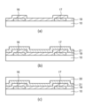
- 2A to 2C are diagrams illustrating a method for manufacturing the semiconductor device 100 according to the first embodiment of the present invention.
- 2A to 2C are diagrams illustrating a method for manufacturing the semiconductor device 100 according to the first embodiment of the present invention.
- 1A to 1C are diagrams illustrating a method for manufacturing a semiconductor device according to a first embodiment of the present invention.
- 1A to 1C are diagrams illustrating a method for manufacturing a semiconductor device according to a first embodiment of the present invention.
- 1 is a cross-sectional TEM image of an epitaxial wafer 10.
- FIG. 2 is a diagram showing the results of elemental analysis of an epitaxial wafer before annealing.
- FIG. 13 is a diagram showing the results of elemental analysis of the epitaxial wafer after annealing.
- Embodiment 1 A power amplifier according to an embodiment of the present disclosure will be described with reference to the drawings. The same or corresponding components are designated by the same reference numerals, and repeated description may be omitted.
- FIG. 1 is a cross-sectional view showing a semiconductor device 100 according to a first embodiment of the present invention.
- the semiconductor device 100 is a GaN-based HEMT formed on an epitaxial wafer 10.
- the epitaxial wafer 10 includes a substrate 11, a channel layer 12, a spacer layer 13, a barrier layer 14, and a cap layer 15.
- the substrate 11 is made of semi-insulating silicon carbide (SiC).
- the thickness of the substrate 11 is, for example, 100 ⁇ m, and the upper surface is, for example, a (0001) surface.
- the material of the substrate 11 may be monolithic sapphire or the like.
- a channel layer 12 made of GaN is formed above the front surface of the substrate 11 .
- a spacer layer 13 is formed above the channel layer 12 in contact with the channel layer 12.
- the spacer layer 13 is made of AlN and has a very thin thickness, preferably 10 nm or less, and more preferably 0.5 nm to 1.5 nm.
- a barrier layer 14 made of AlGaN (aluminum gallium nitride) is formed above the spacer layer 13 .
- a cap layer 15 made of GaN is formed above the barrier layer 14 .
- a source electrode 16, a drain electrode 17, and a gate electrode 18 are provided in contact with the cap layer 15.
- the remaining portion of the cap layer 15 is covered with a protective film 19 mainly made of SiN (silicon nitride).
- a nucleation layer or a buffer layer may be laminated above the substrate 11 before the channel layer 12 is laminated.
- the nucleation layer may be a thin layer made of AlN
- the buffer layer may be a layer made of GaN or AlGaN.
- a two-dimensional electron gas 20 called 2DEG is generated at the interface between the channel layer 12 made of GaN and the spacer layer 13 made of AlGaN.
- the 2DEG is uniformly distributed within the transistor.
- Al in the spacer layer 13 under the gate electrode 18 is diffused into the channel layer 12 and the barrier layer 14 by laser annealing. Therefore, the concentration of the two-dimensional electron gas 20 under the gate electrode 18 is reduced compared to other parts, and the resistance under the gate electrode 18 is increased.
- FIGS. 2 to 5 are diagrams showing a method for manufacturing the semiconductor device 100 according to the first embodiment.
- the method for manufacturing the semiconductor device 100 will be described with reference to FIGS.
- a channel layer 12 is formed above the surface side of a substrate 11
- a spacer layer 13 is formed above the channel layer 12
- a barrier layer 14 is formed above the spacer layer 13
- a cap layer 15 is formed above the barrier layer 14 by epitaxial growth, thereby forming an epitaxial wafer 10.
- a source electrode 16 and a drain electrode 17 are formed on the surface of the epitaxial wafer 10 by deposition, sputtering, plating, or the like.
- a protective film 19 is formed so as to cover the epitaxial wafer 10.
- the material of the protective film 19 is, for example, a silicon nitride film, a silicon oxide film, an aluminum nitride film, or an aluminum oxide film, and is formed by, for example, MOCVD or ALD (Atomic Layer Deposition).
- a metal film 21 is formed so as to cover the protective film 19.
- the metal film 21 is a thin metal film for reflecting a laser 90, which will be described later.
- the material of the metal film 21 is Ni, but this is not limited thereto and may be a metal such as Au.
- a resist 30 is applied so as to cover the metal film 21.
- the resist 30 is removed from the portion where the gate electrode 18 is to be formed, using a so-called photolithography process that is common in semiconductor manufacturing, and an opening 42 is formed in the resist 30.
- an etching process is used to open the metal film 21 exposed from the opening 42, forming an opening 31 in the metal film 21. Furthermore, the protective film 19 is removed to expose the epitaxial wafer 10. The portion of the epitaxial wafer 10 exposed from the opening 31 is defined as an exposed portion 32. The opening 31 and exposed portion 32 are formed to be as fine as the gate electrode 18 using a so-called photolithography process. Next, as shown in FIG. 3(f), the resist 30 is removed by using a wet etching process or a dry etching process.
- a laser 90 is irradiated into the opening 31 to heat the exposed portion 32.
- the wavelength of the laser 90 may be any wavelength that can be absorbed by GaN, AlGaN, AlN, etc., and is generally shorter than 400 nm.
- the metal film 21 is removed by using a wet etching process or a dry etching process.
- openings 44 are openings for forming the gate electrodes 18, and are formed around the openings 31 and exposed portions 32 while exposing the openings 31 and exposed portions 32.
- 5( j ) the gate electrode 18 is formed in the opening 31.
- the gate electrode 18 is formed in contact with the exposed portion 32.
- the resist 33 is removed.
- Figure 6 shows cross-sectional TEM images taken near the interface between the channel layer 12 and spacer layer 13 of the epitaxial wafer 10 before and after annealing, showing how Al in the AlN is diffused by annealing.
- GaN, AlN, and AlGaN in Figure 6 correspond to the channel layer 12, spacer layer 13, and barrier layer 14, respectively.
- Fig. 6(c) is an enlarged view of the vicinity of the GaN/AlN interface in Fig. 6(a)
- Fig. 6(d) is an enlarged view of the vicinity of the GaN/AlN interface in Fig. 6(b).
- FIG. 7 shows the results of elemental analysis of the epitaxial wafer 10 before annealing
- FIG. 8 shows the results of elemental analysis of the epitaxial wafer 10 after annealing.
- the horizontal axis indicates the depth direction distance from the wafer surface, with the left side being the barrier layer 14 side and the right side being the channel layer 12 side. Note that the horizontal axis in FIG. 7 and FIG. 8 does not indicate the absolute distance from the wafer surface, so the positions cannot be directly compared.
- the vertical axis indicates the intensity of the detected elements (Ga, N, Al). Note that only Al is shown with its intensity multiplied by 5.
- the Al intensity in Figure 7 drops sharply over a width of 1.6 nm from the point at a distance of 9.2 nm to the point at a distance of 10.8 nm. That is, it is understood that the Al concentration distribution switches sharply.
- the Al intensity drops over a width of 3 nm from the point at a distance of 7.2 nm to the point at a distance of 10.2 nm. That is, it is understood that the steepness is lost compared to before annealing, and that after annealing, Al in the spacer layer 13 diffuses toward the channel layer 12.
- the Al concentration in the channel layer 12 is overwhelmingly lower than the Al concentration in the barrier layer 14, and therefore it is considered that the amount of Al diffusing from the spacer layer 13 to the channel layer 12 is far greater than the amount of Al diffusing from the spacer layer 13 to the barrier layer 14.
- a laser 90 is irradiated onto the opening 31 where the gate electrode 18 is to be formed, with the metal film 21 remaining except for the opening 31.
- the spacer layer 13 and the channel layer 12 are annealed below the opening 31, Al of the spacer layer 13 is diffused into the channel layer 12, and the concentration of the two-dimensional electron gas 20 is reduced.
- the spacer layer 13 and the channel layer 12 are not annealed except for the lower part of the opening 31, including the lower parts of the source electrode and the drain electrode. Therefore, Al of the spacer layer 13 does not diffuse into the channel layer 12, and the concentration of the two-dimensional electron gas 20 does not decrease.
- the lower part of the opening 31 mentioned here includes not only the area directly below the opening 31 but also the area directly below the opening 31 and its vicinity which is annealed by irradiating the opening 31 with the laser 90 .
- the Al of the spacer layer 13 diffuses into the channel layer 12 below the opening 31, and as a result, the concentration of the two-dimensional electron gas 20 below the opening 31 becomes lower than the concentration of the two-dimensional electron gas 20 elsewhere than below the opening 31.
- the semiconductor device 100 has the advantage that the access resistance is reduced by providing an AlN spacer layer in parts other than the lower part of the gate electrode 18, while the resistance is increased in the lower part of the gate electrode 18, thereby achieving a high withstand voltage. Furthermore, the manufacturing flow of the semiconductor device 100 can avoid the difficulty of removing the thin spacer layer 13 made of AlN by etching.
- the protective film 19 is removed to expose the epitaxial wafer 10, but the protective film 19 may be left thin enough not to affect the annealing of the spacer layer 13 and the channel layer 12 by laser irradiation, and may be removed immediately before forming the gate electrode 18 described in FIG. 5(j).
- the protective film 19 may be left thin enough not to affect the annealing of the spacer layer 13 and the channel layer 12 by laser irradiation, and may be removed immediately before forming the gate electrode 18 described in FIG. 5(j).
Landscapes
- Junction Field-Effect Transistors (AREA)
Priority Applications (3)
| Application Number | Priority Date | Filing Date | Title |
|---|---|---|---|
| CN202380100335.8A CN121533152A (zh) | 2023-07-20 | 2023-07-20 | 半导体装置及其制造方法 |
| JP2023570418A JP7513219B1 (ja) | 2023-07-20 | 2023-07-20 | 半導体装置およびその製造方法 |
| PCT/JP2023/026521 WO2025017892A1 (ja) | 2023-07-20 | 2023-07-20 | 半導体装置およびその製造方法 |
Applications Claiming Priority (1)
| Application Number | Priority Date | Filing Date | Title |
|---|---|---|---|
| PCT/JP2023/026521 WO2025017892A1 (ja) | 2023-07-20 | 2023-07-20 | 半導体装置およびその製造方法 |
Publications (1)
| Publication Number | Publication Date |
|---|---|
| WO2025017892A1 true WO2025017892A1 (ja) | 2025-01-23 |
Family
ID=91802831
Family Applications (1)
| Application Number | Title | Priority Date | Filing Date |
|---|---|---|---|
| PCT/JP2023/026521 Pending WO2025017892A1 (ja) | 2023-07-20 | 2023-07-20 | 半導体装置およびその製造方法 |
Country Status (3)
| Country | Link |
|---|---|
| JP (1) | JP7513219B1 (https=) |
| CN (1) | CN121533152A (https=) |
| WO (1) | WO2025017892A1 (https=) |
Citations (4)
| Publication number | Priority date | Publication date | Assignee | Title |
|---|---|---|---|---|
| JP2000021897A (ja) * | 1998-06-29 | 2000-01-21 | Toshiba Corp | 電界効果トランジスタおよびその製造方法 |
| JP2013062365A (ja) * | 2011-09-13 | 2013-04-04 | Fujitsu Ltd | 化合物半導体装置及びその製造方法 |
| JP2016058546A (ja) * | 2014-09-09 | 2016-04-21 | 株式会社東芝 | 半導体装置 |
| CN111477547A (zh) * | 2020-04-26 | 2020-07-31 | 广东省半导体产业技术研究院 | 一种增强型功率器件及其制作方法 |
-
2023
- 2023-07-20 CN CN202380100335.8A patent/CN121533152A/zh active Pending
- 2023-07-20 JP JP2023570418A patent/JP7513219B1/ja active Active
- 2023-07-20 WO PCT/JP2023/026521 patent/WO2025017892A1/ja active Pending
Patent Citations (4)
| Publication number | Priority date | Publication date | Assignee | Title |
|---|---|---|---|---|
| JP2000021897A (ja) * | 1998-06-29 | 2000-01-21 | Toshiba Corp | 電界効果トランジスタおよびその製造方法 |
| JP2013062365A (ja) * | 2011-09-13 | 2013-04-04 | Fujitsu Ltd | 化合物半導体装置及びその製造方法 |
| JP2016058546A (ja) * | 2014-09-09 | 2016-04-21 | 株式会社東芝 | 半導体装置 |
| CN111477547A (zh) * | 2020-04-26 | 2020-07-31 | 广东省半导体产业技术研究院 | 一种增强型功率器件及其制作方法 |
Also Published As
| Publication number | Publication date |
|---|---|
| CN121533152A (zh) | 2026-02-13 |
| JPWO2025017892A1 (https=) | 2025-01-23 |
| JP7513219B1 (ja) | 2024-07-09 |
Similar Documents
| Publication | Publication Date | Title |
|---|---|---|
| CN209747521U (zh) | 高电子迁移率晶体管 | |
| JP5579980B2 (ja) | 電界効果トランジスタ | |
| JP2008124262A (ja) | 選択再成長を用いたAlGaN/GaN−HEMTの製造方法 | |
| US20140073095A1 (en) | High electron mobility transistor and method of forming the same | |
| TWI680503B (zh) | 氮化鎵高電子移動率電晶體的閘極結構的製造方法 | |
| JP2020017647A (ja) | 半導体装置の製造方法 | |
| CN111009580B (zh) | 高电子迁移率晶体管元件及其制造方法 | |
| TWI535007B (zh) | 半導體裝置與其之製造方法 | |
| JP5101143B2 (ja) | 電界効果トランジスタ及びその製造方法 | |
| US20100207165A1 (en) | Semiconductor device and method for fabricating the same | |
| TWI893315B (zh) | 半導體裝置以及其製作方法 | |
| JP2019212840A (ja) | 半導体装置の製造方法 | |
| JP7513219B1 (ja) | 半導体装置およびその製造方法 | |
| US20240304710A1 (en) | Hemt device having improved on-state performance and manufacturing process thereof | |
| JP4761718B2 (ja) | 半導体装置およびその製造方法 | |
| JP2019135745A (ja) | 電界効果トランジスタの製造方法 | |
| JP2004363346A (ja) | 半導体装置の製造方法 | |
| KR20150100575A (ko) | 실리콘기반 AlGaN/GaN HEMT 소자의 더블덱 오버행 게이트 형성방법 | |
| KR102753349B1 (ko) | 고 전자이동도 트랜지스터 및 그 제조 방법 | |
| CN112310210A (zh) | 高电子迁移率晶体管 | |
| JP5540685B2 (ja) | 化合物半導体装置の製造方法 | |
| CN117276331A (zh) | 高电子迁移率晶体管装置及其制造方法 | |
| US20170092783A1 (en) | Semiconductor device and method of manufacturing the same | |
| JPS6354231B2 (https=) | ||
| JP7640000B1 (ja) | 半導体装置の製造方法 |
Legal Events
| Date | Code | Title | Description |
|---|---|---|---|
| WWE | Wipo information: entry into national phase |
Ref document number: 2023570418 Country of ref document: JP |
|
| NENP | Non-entry into the national phase |
Ref country code: DE |