WO2025013528A1 - 電子装置 - Google Patents
電子装置 Download PDFInfo
- Publication number
- WO2025013528A1 WO2025013528A1 PCT/JP2024/021855 JP2024021855W WO2025013528A1 WO 2025013528 A1 WO2025013528 A1 WO 2025013528A1 JP 2024021855 W JP2024021855 W JP 2024021855W WO 2025013528 A1 WO2025013528 A1 WO 2025013528A1
- Authority
- WO
- WIPO (PCT)
- Prior art keywords
- thickness direction
- chip
- electronic device
- electronic
- pad
- Prior art date
- Legal status (The legal status is an assumption and is not a legal conclusion. Google has not performed a legal analysis and makes no representation as to the accuracy of the status listed.)
- Pending
Links
Images









Classifications
-
- H—ELECTRICITY
- H10—SEMICONDUCTOR DEVICES; ELECTRIC SOLID-STATE DEVICES NOT OTHERWISE PROVIDED FOR
- H10W—GENERIC PACKAGES, INTERCONNECTIONS, CONNECTORS OR OTHER CONSTRUCTIONAL DETAILS OF DEVICES COVERED BY CLASS H10
- H10W72/00—Interconnections or connectors in packages
-
- H—ELECTRICITY
- H10—SEMICONDUCTOR DEVICES; ELECTRIC SOLID-STATE DEVICES NOT OTHERWISE PROVIDED FOR
- H10W—GENERIC PACKAGES, INTERCONNECTIONS, CONNECTORS OR OTHER CONSTRUCTIONAL DETAILS OF DEVICES COVERED BY CLASS H10
- H10W72/00—Interconnections or connectors in packages
- H10W72/071—Connecting or disconnecting
Definitions
- This disclosure relates to electronic devices.
- Patent Document 1 discloses an example of a conventional semiconductor device.
- the semiconductor device described in this document includes a semiconductor element, multiple leads, a bonding material, a wire, and a sealing resin.
- the semiconductor element has a main surface and an electrode arranged on the main surface.
- the semiconductor element is mounted on one of the multiple leads.
- the semiconductor element is bonded to the lead by a bonding material.
- the bonding material is, for example, solder, silver paste, or sintered silver.
- the wire is bonded to the other of the multiple leads and the electrode of the semiconductor element, electrically connecting them.
- the sealing resin covers the semiconductor element.
- An object of the present disclosure is to provide an electronic device that is an improvement over conventional devices.
- an object of the present disclosure is to provide an electronic device that can suppress unintended short circuits through bonding materials, even when a thin electronic chip is used.
- the electronic device provided by the first aspect of the present disclosure includes an electronic chip, a mounting portion on which the electronic chip is mounted, and a joint portion that joins the electronic chip to the mounting portion.
- the electronic chip has a chip main surface facing one side in the thickness direction, a chip back surface facing the other side in the thickness direction, and a chip side surface interposed between the chip main surface and the chip back surface in the thickness direction.
- the first dimension in the thickness direction of the electronic chip is greater than 0 ⁇ m and less than 150 ⁇ m.
- the joint portion has an intermediate portion and an outer peripheral portion, and overlaps 80% to 100% of the periphery of the electronic chip as viewed in the thickness direction.
- the intermediate portion is interposed between the chip back surface and the mounting portion.
- the outer peripheral portion is in contact with at least the other edge of the chip side surface in the thickness direction.
- the second dimension in the thickness direction of the outer peripheral portion is greater than 0 times and less than 2/3 times the first dimension.
- FIG. 1 is a perspective view showing an electronic device according to a first embodiment.
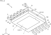
- FIG. 2 is a perspective view of the electronic device according to the first embodiment.
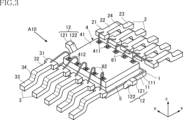
- FIG. 3 is a perspective view of the device shown in FIG. 1 with the sealing member omitted.
- FIG. 4 is a plan view illustrating the electronic device according to the first embodiment.
- FIG. 5 is a front view of the electronic device according to the first embodiment.
- FIG. 6 is a side view of the electronic device according to the first embodiment.
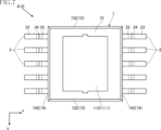
- FIG. 7 is a bottom view illustrating the electronic device according to the first embodiment.
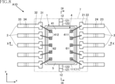
- FIG. 8 is a diagram in which the sealing member is shown by imaginary lines in the plan view shown in FIG.
- FIG. 9 is a cross-sectional view taken along line IX-IX in FIG. FIG.
- FIG. 10 is a cross-sectional view taken along line XX in FIG.
- FIG. 11 is an enlarged plan view of a main portion of FIG. 8, in which the electronic chip is shown by imaginary lines and a number of connecting members are omitted.
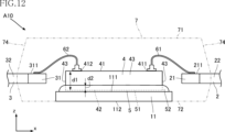
- FIG. 12 is an enlarged front view of a main portion of FIG. 5, in which the sealing member is indicated by imaginary lines.
- FIG. 13 is an enlarged cross-sectional view of a main portion of FIG.
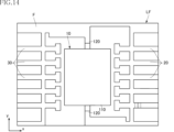
- FIG. 14 is a plan view showing a step of the method for manufacturing the electronic device according to the first embodiment.
- FIG. 15 is a plan view showing a step of the method for manufacturing the electronic device according to the first embodiment.
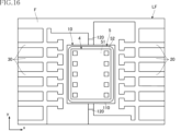
- FIG. 16 is a plan view showing a step of the method for manufacturing the electronic device according to the first embodiment.
- FIG. 17 is a plan view showing a step of the method for manufacturing the electronic device according to the first embodiment.
- FIG. 18 is a cross-sectional view showing an electronic device according to a first modified example of the first embodiment.
- FIG. 19 is a cross-sectional view showing an electronic device according to a second modification of the first embodiment.
- FIG. 20 is an enlarged plan view of a main part of an electronic device according to the second embodiment.
- FIG. 21 is an enlarged plan view of a main part of an electronic device according to a modified example of the second embodiment.
- FIG. 22 is a front view showing the electronic device according to the third embodiment, in which the sealing member is shown by imaginary lines.
- FIG. 23 is a front view showing an electronic device according to a modified example of the third embodiment, in which a sealing member is shown by imaginary lines.
- an object A is formed on an object B
- an object A is formed on (an object B)
- an object A is formed directly on an object B
- an object A is formed on an object B with another object interposed between the object A and the object B” unless otherwise specified.
- an object A is disposed on an object B” and “an object A is disposed on (an object B)” include “an object A is disposed directly on an object B” and “an object A is disposed on (an object B) with another object interposed between the object A and the object B” unless otherwise specified.
- an object A is located on (an object B) includes “an object A is in contact with an object B and is located on (an object B)” and “an object A is located on (an object B) with another object interposed between the object A and the object B".
- an object A overlaps an object B includes “an object A overlaps the entire object B” and “an object A overlaps a part of an object B” unless otherwise specified.
- An object A (its material) contains a certain material C includes “an object A (its material) is made of a certain material C” and “an object A (its material) is mainly composed of a certain material C.”
- a certain surface A faces a certain direction B (one side or the other side of a certain direction B) includes, unless otherwise specified, not limited to the case where the angle of surface A with respect to direction B is 90°, and includes the case where surface A is inclined with respect to direction B.
- a certain surface A is perpendicular to a certain surface B includes, unless otherwise specified, not limited to the case where the angle of surface A with respect to surface B is 90°, and includes the case where surface A is inclined with respect to surface B.
- First embodiment: 1 to 13 show an electronic device A10 according to a first embodiment.
- the electronic device A10 includes a plurality of leads 1, 2, and 3, an electronic chip 4, a joint 5, a plurality of connection members 61 and 62, and a sealing member 7.
- the package structure of the electronic device A10 is not limited in any way, but is a small outline package (SOP) in the illustrated example.
- the package structure of the electronic device A10 may be a leadless type.
- the thickness direction z corresponds to the thickness direction of the electronic device A10.
- Planar view refers to the view in the thickness direction z.
- the first direction x is perpendicular to the thickness direction z.
- the second direction y is perpendicular to the thickness direction z and the first direction x.
- one side of the thickness direction z may be referred to as the upper side, and the other side of the thickness direction z may be referred to as the lower side.
- the terms “upper”, “lower”, “upper”, “lower”, “top surface”, and “bottom surface” indicate the relative positional relationship of each component, etc. in the thickness direction z, and are not necessarily terms that define the relationship with the direction of gravity.
- the lead 1 supports the electronic chip 4.
- the lead 1 is formed by subjecting a metal plate material such as copper (Cu) or a Cu alloy to processes such as cutting and bending.
- a metal plate material such as copper (Cu) or a Cu alloy to processes such as cutting and bending.
- the lead 1 of this embodiment includes a mounting portion 11 and two extending portions 12.
- the extending portions 12 are omitted in Figure 12.
- the mounting portion 11 is mounted with an electronic chip 4.
- the planar shape of the mounting portion 11 is not limited in any way, but in the illustrated example, it is rectangular.
- the mounting portion 11 has a main mounting surface 111 and a back mounting surface 112.
- the main mounting surface 111 faces one side in the thickness direction z (upward in the thickness direction z).
- the main mounting surface 111 is covered by a sealing member 7.
- the back mounting surface 112 faces the other side in the thickness direction z (downward in the thickness direction z).
- the back mounting surface 112 is exposed from the sealing member 7. This can promote heat dissipation from the electronic chip 4.
- the two extension portions 12 extend from the mounting portion 11 to both sides in the second direction y, as shown in Figures 8 and 9.
- the lead 1 may include two or more extension portions 12.
- the lead 1 includes four extension portions 12, which extend outward in the second direction y from near the four corners of the mounting portion 11 in a plan view.
- Each of the two extension portions 12 includes a tip portion 121 and a connection portion 122, as shown in Figures 8 and 9.
- the tip portion 121 and the connection portion 122 described below are common to each extension portion 12 unless otherwise specified.
- the tip 121 is located on both outer sides of the mounting portion 11 in the second direction y, and is located in the thickness direction z on the side of the mounting portion 11 where the main mounting surface 111 faces (upward in the thickness direction z).
- the shape of the tip 121 is not limited in any way, but in the illustrated example, it has a shape with a constant (or approximately constant) dimension (width) in the first direction x.
- the dimension of the tip 121 in the first direction x is smaller than the dimension of the mounting portion 11 in the first direction x.
- connection portion 122 is connected to and connects the mounting portion 11 and the tip portion 121.
- the connection portion 122 is covered by a sealing member 7.
- the connection portion 122 is inclined with respect to the second direction y (x-y plane).
- the dimension of the connection portion 122 in the first direction x is not limited in any way, but is, for example, the same as the dimension of the tip portion 121 in the first direction x.
- the multiple leads 2, 3 are used as terminals for mounting the electronic device A10, and are electrically connected to the electronic chip 4.
- Each of the multiple leads 2, 3 is formed by subjecting a metal plate material such as Cu or a Cu alloy to cutting and bending processes.
- Each of the multiple leads 2, 3 is separated from the mounting portion 11, as shown in Figures 8 and 10.
- each of the multiple leads 2 is arranged on one side of the first direction x with respect to the mounting portion 11.
- the multiple leads 2 are arranged at equal pitches along the second direction y.
- the dimension of each lead 2 in the thickness direction z is not limited in any way, but is, for example, the same as the dimension of the lead 1 in the thickness direction z.
- each of the multiple leads 2 includes a portion covered by the sealing member 7 and a portion exposed from the sealing member 7. In each lead 2, the portion exposed from the sealing member 7 is formed in a gull-wing shape as shown in FIGS. 5 and 10.
- Each of the multiple leads 2 includes a first pad portion 21, a strip portion 22, a terminal portion 23, and a connection portion 24. The first pad portion 21, strip portion 22, terminal portion 23, and connection portion 24 described below are common to each lead 2 unless otherwise specified.
- the first pad portion 21 is covered with a sealing member 7 as shown in Figs. 8 and 10.
- the first pad portion 21 is located on the side of the mounting portion 11 in the thickness direction z where the main mounting surface 111 faces (upward in the thickness direction z).
- the first pad portion 21 has a first pad surface 211.
- the first pad surface 211 faces one side in the thickness direction z (upward in the thickness direction z).
- a connection member 61 is bonded to the first pad surface 211.
- the first pad surface 211 and the main mounting surface 111 are offset in the thickness direction z.
- the first pad surface 211 is located on the side of the main mounting surface 111 in the thickness direction z where the main mounting surface 111 faces (upward in the thickness direction z).
- the band-shaped portion 22 extends outward from the sealing member 7 from the first pad portion 21.
- the band-shaped portion 22 includes a portion covered by the sealing member 7 and a portion exposed from the sealing member 7.
- the dimension of the band-shaped portion 22 in the second direction y is not limited in any way, but is smaller than the dimension of the first pad portion 21 in the second direction y, for example. Unlike this example, the dimension of the first pad portion 21 in the second direction y and the dimension of the band-shaped portion 22 in the second direction y may be the same.
- the terminal portion 23 is located outward in the first direction x with respect to the first pad portion 21 and the band portion 22.
- the terminal portion 23 is located on the other side of the thickness direction z (below the thickness direction z) with respect to the first pad portion 21 and the band portion 22.
- the terminal portion 23 is exposed from the sealing member 7.
- the dimension of the terminal portion 23 in the second direction y is not limited in any way, but is, for example, the same as the dimension of the band portion 22 in the second direction y. In the illustrated example, the terminal portion 23 overlaps the mounting portion 11 when viewed in the first direction x.
- connection portion 24 is interposed between the band portion 22 and the terminal portion 23.
- the connection portion 24 is connected to the band portion 22 and the terminal portion 23, and connects them.
- the connection portion 24 is exposed from the sealing member 7.
- the connection portion 24 is inclined with respect to the first direction x (xy plane).
- the dimension of the connection portion 24 in the second direction y is not limited in any way, but is, for example, the same as the dimension of the band portion 22 in the second direction y and the dimension of the terminal portion 23 in the second direction y.
- each of the multiple leads 3 is disposed on the other side of the first direction x with respect to the mounting portion 11. Therefore, the multiple leads 3 are disposed on the opposite side of the multiple leads 2 in the first direction x, sandwiching the mounting portion 11 therebetween.
- the multiple leads 3 are disposed at equal pitches along the second direction y.
- the dimension of each lead 3 in the thickness direction z is not limited in any way, but is, for example, the same as the dimension of each lead 2 in the thickness direction z.
- Each of the multiple leads 3 includes a portion covered by the sealing member 7 and a portion exposed from the sealing member 7, as shown in FIG. 4, FIG. 5, FIG. 7, FIG. 8, and FIG. 10.
- each lead 3 the portion exposed from the sealing member 7 is formed in a gull-wing shape, as shown in FIG. 5 and FIG. 10.
- Each of the multiple leads 3 includes a second pad portion 31, a strip portion 32, a terminal portion 33, and a connection portion 34.
- the second pad portion 31, the strip portion 32, the terminal portion 33, and the connection portion 34 described below are common to each lead 3 unless otherwise specified.
- the second pad portion 31 is covered with a sealing member 7 as shown in Figs. 8 and 10.
- the second pad portion 31 is located on the side of the mounting portion 11 where the main mounting surface 111 faces in the thickness direction z (upward in the thickness direction z).
- the second pad portion 31 has a second pad surface 311.
- the second pad surface 311 faces one side in the thickness direction z (upward in the thickness direction z).
- a connection member 62 is bonded to the second pad surface 311.
- the second pad surface 311 and the main mounting surface 111 are offset in the thickness direction z.
- the second pad surface 311 is located on the side of the main mounting surface 111 where the main mounting surface 111 faces in the thickness direction z (upward in the thickness direction z).
- the second pad surface 311 is located at the same position as the first pad surface 211 in the thickness direction z.
- the band-shaped portion 32 extends outward from the second pad portion 31 to the outside of the sealing member 7.
- the band-shaped portion 32 includes a portion covered by the sealing member 7 and a portion exposed from the sealing member 7.
- the dimension of the band-shaped portion 32 in the second direction y is not limited in any way, but is smaller than the dimension of the second pad portion 31 in the second direction y. Unlike this example, the dimension of the second pad portion 31 in the second direction y and the dimension of the band-shaped portion 32 in the second direction y may be the same.
- the terminal portion 33 is located outward in the first direction x with respect to the second pad portion 31 and the band portion 32.
- the terminal portion 33 is located on the other side of the thickness direction z (below the thickness direction z) with respect to the second pad portion 31 and the band portion 32.
- the terminal portion 33 is exposed from the sealing member 7.
- the dimension of the terminal portion 33 in the second direction y is not limited in any way, but is, for example, the same as the dimension of the band portion 22 in the second direction y. In the illustrated example, the terminal portion 33 overlaps the mounting portion 11 when viewed in the first direction x.
- connection portion 34 is interposed between the band portion 32 and the terminal portion 33.
- the connection portion 34 is connected to the band portion 32 and the terminal portion 33, and connects them.
- the connection portion 34 is exposed from the sealing member 7.
- the connection portion 34 is inclined with respect to the first direction x (xy plane).
- the dimension of the connection portion 34 in the second direction y is not limited in any way, but is, for example, the same as the dimension of the band portion 32 in the second direction y and the dimension of the terminal portion 33 in the second direction y.
- the electronic chip 4 is an element that performs the main electrical functions in the electronic device A10.
- Specific examples of the electronic chip 4 are not limited, but include, for example, an LSI or an IC. Unlike this example, the electronic chip 4 may be a discrete component such as a diode, an inductor, or a transistor.
- the specific shape and size of the electronic chip 4 are not limited, but as shown in Figures 3 and 8, in this embodiment, for example, the electronic chip 4 is rectangular in plan view and smaller than the mounting portion 11. Since the shape of the electronic chip 4 in plan view is rectangular, the periphery 44 of the electronic chip 4 in plan view is rectangular.
- the first dimension d1 of the electronic chip 4 in the thickness direction z is, for example, greater than 0 ⁇ m and equal to or less than 150 ⁇ m.
- the first dimension d1 of the electronic chip 4 may be greater than 0 ⁇ m and equal to or less than 100 ⁇ m.
- the electronic chip 4 has a chip main surface 41, a chip back surface 42, and multiple chip side surfaces 43.
- the chip main surface 41 faces one side of the thickness direction z (upward in the thickness direction z).
- the chip back surface 42 faces the other side of the thickness direction z (downward in the thickness direction z).
- the chip back surface 42 faces the mounting main surface 111.
- Each of the multiple chip side surfaces 43 is interposed between the chip main surface 41 and the chip back surface 42 in the thickness direction z.
- the multiple chip side surfaces 43 include a pair of chip side surfaces 43 facing both sides of the first direction x and a pair of chip side surfaces 43 facing both sides of the second direction y.
- Each chip side surface 43 is perpendicular to the chip main surface 41 and the chip back surface 42.
- a plurality of electrode pads 411, 412 are provided on the chip main surface 41.
- the plurality of electrode pads 411 are arranged on the chip main surface 41 along the second direction y.
- the plurality of electrode pads 411 are arranged on the chip main surface 41 on the side of the plurality of leads 2 in the first direction x.
- the plurality of electrode pads 412 are arranged on the chip main surface 41 along the second direction y.
- the plurality of electrode pads 412 are arranged on the chip main surface 41 on the side of the plurality of leads 3 in the first direction x.
- the electronic chip 4 includes multiple corners 45 in a planar view.
- the electronic chip 4 includes four corners 45.
- Each corner 45 is the boundary between two chip side surfaces 43 that are connected to each other.
- the joint 5 joins the electronic chip 4 to the mounting portion 11.
- the joint 5 is, for example, silver paste.
- the joint 5 may be other conductive joining materials such as solder or sintered silver instead of silver paste.
- the joint 5 overlaps 80% to 100% of the periphery 44 of the electronic chip 4 in a planar view.
- the joint 5 overlaps the entire periphery 44 of the electronic chip 4 (i.e., 100%) in a planar view.
- the joint 5 includes an intermediate portion 51 and an outer periphery 52.
- the intervening portion 51 is interposed between the chip back surface 42 and the main mounting surface 111.
- the third dimension d3 of the intervening portion 51 in the thickness direction z is not limited in any way, but is, for example, 20 ⁇ m or more and 30 ⁇ m or less.
- the outer peripheral portion 52 is arranged around the intermediate portion 51 over the entire circumference of the intermediate portion 51 in a planar view.
- the outer peripheral portion 52 is connected to the intermediate portion 51.
- the outer peripheral portion 52 is arranged outside the electronic chip 4 in a planar view.
- the outer peripheral portion 52 contacts at least the lower edge of each chip side surface 43 in the thickness direction z.
- the outer peripheral portion 52 contacts a portion of the lower side of each chip side surface 43 in the thickness direction z.
- the outer peripheral portion 52 creeps upward in the thickness direction z along each chip side surface 43.
- the second dimension d2 in the thickness direction z of the outer peripheral portion 52 is, for example, 0 times or more and 2/3 times or less than the first dimension d1 of the electronic chip 4.
- the second dimension d2 of the outer peripheral portion 52 is 0 ⁇ m or more and 66.6 ⁇ m or less.
- the second dimension d2 (in the thickness direction z) of the outer periphery 52 is the dimension (creeping up dimension) of the portion that rises upward in the thickness direction z from the bottom end of the electronic chip 4 in the thickness direction z as shown in Figures 9, 12, and 13.
- the outer peripheral portion 52 includes a plurality of side covering portions 521 and a plurality of ridge covering portions 522.
- the plurality of side covering portions 521 contact at least the lower edge in the thickness direction z of a corresponding one of the plurality of chip side surfaces 43, and cover a portion of the corresponding chip side surface 43.
- Each side covering portion 521 creeps up along the corresponding chip side surface 43 from the lower edge in the thickness direction z to halfway in the thickness direction z.
- the plurality of ridge covering portions 522 each individually cover a portion of the plurality of corner portions 45.
- Each ridge covering portion 522 creeps up along the corresponding corner portion 45 from the lower edge in the thickness direction z to halfway in the thickness direction z.
- the plurality of side covering portions 521 and the plurality of ridge covering portions 522 are connected.
- the multiple connection members 61, 62 each electrically connect parts spaced apart from each other.
- the multiple connection members 61, 62 are each bonding wires.
- the multiple connection members 61, 62 may not be bonding wires, but may be metal plates.
- the multiple connection members 61, 62 each contain, for example, gold, aluminum, Cu, or the like.
- the multiple connection members 61 are each individually bonded to the multiple electrode pads 411 and the first pad portions 21 (first pad surfaces 211) of the multiple leads 2.
- the multiple connection members 62 are each individually bonded to the multiple electrode pads 412 and the second pad portions 31 (second pad surfaces 311) of the multiple leads 3.
- the sealing member 7 covers a portion of the lead 1, each of the multiple leads 2, each of the multiple leads 3, the electronic chip 4, the joint 5, and the multiple connection members 61, 62.
- the sealing member 7 is made of an insulating resin, for example a black epoxy resin containing a filler.
- the sealing member 7 has a resin main surface 71, a resin back surface 72, a pair of resin side surfaces 73, and a pair of resin side surfaces 74.
- the resin main surface 71 faces one side in the thickness direction z (upward in the thickness direction z).
- the resin back surface 72 faces the other side in the thickness direction z (downward in the thickness direction z).
- the resin main surface 71 is rectangular in plan view.
- the mounting back surface 112 is exposed from the resin back surface 72, and the resin back surface 72 has an annular shape in plan view.
- the outer edge of the resin back surface 72 is rectangular.
- the pair of resin side surfaces 73 are located between the resin main surface 71 and the resin back surface 72, and are located on both sides of the second direction y.
- the pair of resin side surfaces 73 face opposite each other in the second direction y.
- Each of the pair of resin side surfaces 73 has an upper region 731, a lower region 732, and an intermediate region 733.
- the upper region 731, lower region 732, and intermediate region 733 described below are common to each resin side surface 73, unless otherwise specified.
- the upper region 731 is a region located between the resin main surface 71 and the intermediate region 733 in the thickness direction z.
- the upper region 731 is inclined with respect to a plane (x-z plane) perpendicular to the second direction y, but the upper region 731 may also be parallel to the x-z plane.
- the lower region 732 is a region located between the resin back surface 72 and the intermediate region 733 in the thickness direction z, as shown in Figures 5, 6, and 9.
- the lower region 732 is inclined with respect to a plane (x-z plane) perpendicular to the second direction y, but the lower region 732 may also be parallel to the x-z plane.
- the intermediate region 733 is a region located between the upper region 731 and the lower region 732 in the thickness direction z.
- the intermediate region 733 is parallel to a plane (xz plane) perpendicular to the second direction y.
- the intermediate region 733 is located outside the second direction y with respect to the resin main surface 71 and the resin back surface 72.
- the upper edge of the intermediate region 733 in the thickness direction z is at the same position in the thickness direction z as the upper edge of the tip portion 121 in the thickness direction z.
- the lower edge of the intermediate region 733 in the thickness direction z is at the same position in the thickness direction z as the lower edge of the tip portion 121 in the thickness direction z. Therefore, the dimension of the intermediate region 733 in the thickness direction z is the same as the dimension of the tip portion 121 in the thickness direction z.
- the pair of resin side surfaces 74 are located between the resin main surface 71 and the resin back surface 72, and are located on both sides of the first direction x.
- One of the pair of resin side surfaces 74 faces the opposite side in the first direction x.
- Each of the pair of resin side surfaces 74 has an upper region 741, a lower region 742, and an intermediate region 743.
- the upper region 741, lower region 742, and intermediate region 743 described below are common to each resin side surface 74, unless otherwise specified.
- the upper region 741 is a region located between the resin main surface 71 and the intermediate region 743 in the thickness direction z.
- the upper region 741 is inclined with respect to a plane (y-z plane) perpendicular to the first direction x, but the upper region 741 may also be parallel to the y-z plane.
- the lower region 742 is a region located between the resin back surface 72 and the intermediate region 743 in the thickness direction z, as shown in Figures 5, 6, and 10.
- the lower region 742 is inclined with respect to a plane (y-z plane) perpendicular to the first direction x, but the lower region 742 may be parallel to the y-z plane.
- the intermediate region 743 is a region located between the upper region 741 and the lower region 742 in the thickness direction z, as shown in Figures 5, 6, and 10.
- the intermediate region 743 is parallel to a plane (y-z plane) perpendicular to the first direction x.
- the intermediate region 743 is located outside the first direction x with respect to the resin main surface 71 and the resin back surface 72.
- the upper edge of the intermediate region 743 in the thickness direction z is at the same position in the thickness direction z as the upper edge of each strip portion 22, 32 in the thickness direction z.
- the lower edge of the intermediate region 743 in the thickness direction z is at the same position in the thickness direction z as the lower edge of each strip portion 22, 32 in the thickness direction z. Therefore, the dimension of the intermediate region 743 in the thickness direction z is the same as the dimension of each strip portion 22, 32 in the thickness direction z.
- Figures 14 to 17 are plan views showing a step in the method for manufacturing electronic device A10.
- the lead frame LF includes a frame F and a lead 10, a plurality of leads 20, and a plurality of leads 30 connected to the frame F.
- the lead 10, the plurality of leads 20, and the plurality of leads 30 are portions of the lead frame LF that are cut from the frame F and bent to become the lead 1, the plurality of leads 2, and the plurality of leads 3.
- the lead 10 includes a mounting portion 110 and two extending portions 120.
- the mounting portion 110 is a portion that becomes the mounting portion 11 of the electronic device A10, and the two extending portions 120 are portions that become the two extending portions 12 of the electronic device A10.
- each extending portion 120 is bent downward in the thickness direction z. Therefore, in the lead frame LF, the mounting portion 110 is located below the plurality of leads 20, the plurality of leads 30, and the frame F in the thickness direction z.
- the paste-like bonding material 50 is applied onto the mounting portion 11.
- the paste-like bonding material 50 is, for example, a silver paste.
- the paste-like bonding material 50 may be a solder paste or a sintered silver paste instead of a silver paste.
- the paste-like bonding material 50 is applied linearly, for example, along six application tracks L1 to L6 shown in FIG. 15, by a dispenser. Each of the six application tracks L1 to L6 is a track of the paste-like bonding material 50 applied by the dispenser.
- the application tracks L1 and L2 are tracks along the diagonal of the electronic chip 4 to be mounted later. In the example shown in FIG.
- the electronic chip 4 is placed on the bonding material paste 50, and the bonding material paste 50 is solidified.
- the weight of the electronic chip 4 spreads the bonding material paste 50.
- the bonding material paste 50 may be spread not only by the weight of the electronic chip 4, but also by the pressing force of a die bonder that places the electronic chip 4.
- the spread bonding material paste 50 has a shape that protrudes outward over the entire periphery of the electronic chip 4 in a plan view, as shown in FIG. 16. That is, the bonding material paste 50 at this time has the same (or approximately the same) plan view shape as the bonding portion 5 of the electronic device A10.
- the bonding material paste 50 is then heat-treated to solidify the bonding material paste 50 and form the bonding portion 5.
- connection members 61, 62 are formed.
- the plurality of connection members 61, 62 are formed by a well-known wire bonder.
- the sealing member 7 shown by the imaginary line (two-dot chain line) in FIG. 17 is formed, for example, by molding.
- each of the leads 10, 20, 30 is cut from the frame F at the cutting line CL (one-dot chain line), and each of the leads 20, 30 is bent. This completes the manufacture of the electronic device A10 shown in FIGS. 1 to 13.
- the first dimension d1 in the thickness direction z of the electronic chip 4 is greater than 0 ⁇ m and less than 150 ⁇ m.
- the joint 5 includes an outer periphery 52 that contacts the chip side surface 43, and the second dimension d2 in the thickness direction z of the outer periphery 52 is greater than 0 times and less than 2/3 times the first dimension d1 of the electronic chip 4. With this configuration, the outer periphery 52 of the joint 5 does not creep up to the chip main surface 41 of the electronic chip 4. Therefore, even if the electronic device A10 has a thin electronic chip 4, it is possible to suppress unintended short circuits through the joint 5.
- joint 5 overlaps 80% to 100% of periphery 44 of electronic chip 4 when viewed in thickness direction z. This configuration allows proper visual inspection of whether electronic chip 4 is joined to mounting portion 11 by joint 5. This configuration ensures an appropriate bonding strength of joint 5 to electronic chip 4 to mounting portion 11.
- the second dimension d2 of the outer periphery 52 is greater than 0 times the first dimension d1 of the electronic chip 4 at the corner 45 of the electronic chip 4 as viewed in the thickness direction z.
- a fillet is formed at the joint 5 at the corner 45 of the electronic chip 4.
- the outer periphery 52 includes a ridge covering portion 522 that covers a part of the corner 45 of the electronic chip 4.
- the outer peripheral portion 52 includes the edge covering portion 522 that covers a part of the corner portion 45 of the electronic chip 4, and therefore the resistance of the joint 5 near the four corners on the lower side in the thickness direction z of the electronic chip 4 to peeling and damage can be improved. Therefore, according to the electronic device A10, peeling and damage of the joint 5 can be suppressed, and therefore reliability can be improved.
- the third dimension d3 in the thickness direction z of the interposed portion 51 is 20 ⁇ m or more and 30 ⁇ m or less. With this configuration, it is possible to ensure an appropriate bonding strength between the electronic chip 4 and the mounting portion 11.
- the paste-like bonding material 50 is applied by a dispenser.
- the paste-like bonding material 50 can also be applied using a printing mask.
- the first pad surface 211 of the first pad portion 21 is located in the thickness direction z in the direction in which the main mounting surface 111 faces (above the thickness direction z) relative to the main mounting surface 111 of the mounting portion 11. Therefore, in an application method using a printing mask, the printing mask comes into contact with the first pad portion 21 and the paste-like bonding material 50 cannot be applied properly.
- the paste-like bonding material 50 is applied by a dispenser, so that the paste-like bonding material 50 can be applied properly even in a structure in which the mounting portion 11 is disposed below the first pad portion 21 in the thickness direction z.
- the first pad surface 211 of the first pad portion 21 and the second pad surface 311 of the second pad portion 31 are disposed at the same position in the thickness direction z, and the first pad portion 21 and the second pad portion 31 are disposed on opposite sides of the mounting portion 11 in the first direction x.
- FIG. 18 shows an electronic device A11 according to a first modified example of the first embodiment.
- the electronic device A11 differs from the electronic device A10 in the following respect. That is, in the electronic device A11, the main mounting surface 111, the first pad surface 211, and the second pad surface 311 are located at the same position in the thickness direction z.
- the first pad portion 21 of each lead 2 overlaps the mounting portion 11 when viewed in the first direction x.
- the second pad portion 31 of each lead 3 overlaps the mounting portion 11 when viewed in the first direction x.
- the main mounting surface 111 is not misaligned with the first pad surface 211 and the second pad surface 311 in the thickness direction z.
- the second dimension d2 in the thickness direction z of the outer periphery 52 of joint 5 is between 0 and 2/3 times the first dimension d1 of the electronic chip 4. Therefore, like electronic device A10, electronic device A11 does not have outer periphery 52 of joint 5 extending up to the chip main surface 41 of the electronic chip 4, so that even with a thin electronic chip 4, unintended short circuits through joint 5 can be suppressed.
- electronic device A11 has a common configuration with electronic device A10, and thus achieves the same effects as electronic device A10.
- FIG. 19 shows an electronic device A12 according to a second modified example of the first embodiment.
- the electronic device A12 differs from the electronic device A10 in the following respect. That is, in the electronic device A12, the main mounting surface 111 is located in the direction in which the main mounting surface 111 faces in the thickness direction z (i.e., upward in the thickness direction z) relative to the first pad surface 211 and the second pad surface 311.
- each lead 2 and each lead 3 is not bent and is rectangular when viewed in the second direction y, but may be bent similarly to electronic device A10.
- the second dimension d2 in the thickness direction z of outer periphery 52 of joint 5 is between 0 and 2/3 times the first dimension d1 of electronic chip 4. Therefore, like electronic device A10, electronic device A12 does not have outer periphery 52 of joint 5 extending up to chip main surface 41 of electronic chip 4, so that even with a thin electronic chip 4, unintended short circuits through joint 5 can be suppressed.
- electronic device A12 has a common configuration with other electronic devices A10 and A11, and thus achieves the same effects as electronic devices A10 and A11.
- Second embodiment: 20 shows an electronic device A20 according to the second embodiment.
- the electronic device A20 is different from the electronic device A10 in the shape of the joint 5 in a plan view.
- the periphery 53 of the joint 5 includes a pair of edges 531 and a pair of edges 532.
- the pair of edges 531 are spaced apart from each other in the first direction x.
- Each of the pair of edges 531 extends in the second direction y.
- the center of each edge 531 in the second direction y is recessed into the electronic chip 4 in a planar view.
- the pair of edges 532 are spaced apart from each other in the second direction y.
- Each of the pair of edges 532 extends in the first direction x.
- the center of each edge 532 in the first direction x is recessed into the electronic chip 4 in a planar view.
- the percentage of the joint 5 that overlaps the periphery 44 of the electronic chip 4 in a planar view is 80% or more and less than 100%. In this way, even if the joint 5 does not overlap 100% of the periphery 44 of the electronic chip 4 in a planar view, as long as it overlaps 80% or more, it is possible to check by visual inspection whether the electronic chip 4 is joined to the mounting portion 11 by the joint 5.
- the amount of the paste-like bonding material 50 applied on both sides of the first direction x and at the center in the second direction y, and the amount of the paste-like bonding material 50 applied on both sides of the second direction y and at the center in the first direction x are not relatively smaller than other portions. Therefore, when the paste-like bonding material 50 is spread out by placing the electronic chip 4, the center of each edge 531 in the second direction y may be recessed into the electronic chip 4 in a plan view, and the center of each edge 532 in the first direction x may be recessed into the electronic chip 4 in a plan view.
- the second dimension d2 in the thickness direction z of outer periphery 52 of joint 5 is between 0 and 2/3 times the first dimension d1 of electronic chip 4. Therefore, similar to electronic device A10, in electronic device A20, outer periphery 52 of joint 5 does not extend up to chip main surface 41 of electronic chip 4, so that even with a thin electronic chip 4, unintended short circuits through joint 5 can be suppressed.
- electronic device A20 has a common configuration with other electronic devices A10-A12, and thus achieves the same effects as electronic devices A10-A12.
- FIG. 21 shows an electronic device A21 according to a modified example of the second embodiment.
- the electronic device A21 differs from the electronic device A20 in the following respect: the entire edge 532 is located outside the electronic chip 4 in a plan view.
- the center of each edge 531 in the second direction y is recessed into the electronic chip 4 in plan view, similar to electronic device A20.
- the center of each edge 532 in the first direction x is located outside the electronic chip 4 in plan view, unlike electronic device A20.
- the proportion of joint 5 that overlaps with the periphery 44 of the electronic chip 4 in plan view is 80% or more and less than 100%.
- the joint 5 in electronic device A21 has the shape shown in the figure for the same reasons as the joint 5 in electronic device A20.
- electronic device A21 similar to electronic device A20 (A10), the second dimension d2 in the thickness direction z of outer periphery 52 of joint 5 is between 0 and 2/3 times the first dimension d1 of electronic chip 4. Therefore, similar to electronic device A20 (A10), electronic device A21 does not have outer periphery 52 of joint 5 extending up to chip main surface 41 of electronic chip 4, so that unintended short circuit via joint 5 can be suppressed even with a thin electronic chip 4.
- electronic device A21 has a common configuration with other electronic devices A10-A12, A20, and thus achieves the same effects as electronic devices A10-A12, A20.
- Fig. 22 shows an electronic device A30 according to the third embodiment.
- the electronic device A30 is different from the electronic device A10 in the following respect.
- the outer periphery 52 of the bonding portion 5 is in contact only with the lower edge in the thickness direction z of each chip side surface 43.
- the extension portion 12 is omitted.
- the second dimension d2 of the outer periphery 52 of the joint 5 is 0 ⁇ m, which is 0 times the first dimension d1 of the electronic chip 4. In other words, the outer periphery 52 does not creep up against the electronic chip 4.
- the upper edge in the thickness direction z of the outer periphery 52 is at the same position in the thickness direction z as the lower edge in the thickness direction z of each chip side surface 43.
- the planar shape of the joint 5 of electronic device A30 may be the same as the planar shape of the joint 5 of electronic device A10 (see FIG. 11), or the same as the planar shape of the joint 5 of electronic device A20 (see FIG. 20) or the planar shape of the joint 5 of electronic device A21 (see FIG. 21).
- the second dimension d2 in the thickness direction z of outer periphery 52 of joint 5 is between 0 and 2/3 times the first dimension d1 of electronic chip 4. Therefore, like electronic device A10, electronic device A30 does not have outer periphery 52 of joint 5 extending up to chip main surface 41 of electronic chip 4, so that even with a thin electronic chip 4, unintended short circuits through joint 5 can be suppressed.
- electronic device A30 has a common configuration with other electronic devices A10-A12, A20, A21, and thus achieves the same effects as electronic devices A10-A12, A20, A21.
- FIG. 23 shows electronic device A31 according to a modified example of the third embodiment.
- Electronic device A31 differs from electronic device A30 in the following respect. That is, the joint 5 of electronic device A31 includes a portion where the second dimension d2 of the outer periphery 52 is 0 times the first dimension d1 of the electronic chip 4, and a portion where the second dimension d2 of the outer periphery 52 is greater than 0 times the first dimension d1 of the electronic chip 4.
- the extension 12 is omitted from FIG. 23.
- the portion where the second dimension d2 of the outer periphery 52 is 0 times the first dimension d1 of the electronic chip 4 is the center in the first direction x. In this way, the second dimension d2 of the outer periphery 52 does not have to be the same size around the entire periphery 44 of the electronic chip 4.
- electronic device A31 like electronic device A30 (A10), the second dimension d2 in the thickness direction z of the outer periphery 52 of joint 5 is between 0 and 2/3 times the first dimension d1 of the electronic chip 4. Therefore, in electronic device A31, like electronic device A30 (A10), the outer periphery 52 of joint 5 does not extend up to the chip main surface 41 of the electronic chip 4, so that even with a thin electronic chip 4, unintended short circuits through joint 5 can be suppressed.
- electronic device A31 has a common configuration with other electronic devices A10-A12, A20, A21, A30, and thus achieves the same effects as electronic devices A10-A12, A20, A21, A30.
- the mounting portion 11 is made of a metal plate material (lead 1), but this is not limited to this.
- the mounting portion 11 may be configured to include an insulating substrate such as a semiconductor substrate, a glass substrate, or a ceramic substrate, and a wiring pattern formed on the insulating substrate.
- the first pad portion 21 and the second pad portion 31 are not limited to being made of a metal plate material (each lead 2 or each lead 3), and may be configured to include an insulating substrate and a wiring pattern formed on the insulating substrate.
- the electronic device according to the present disclosure is not limited to the above-described embodiment.
- the specific configuration of each part of the electronic device according to the present disclosure can be freely designed in various ways.
- the present disclosure includes the embodiments described in the following appendices. Appendix 1.
- a joining portion for joining the electronic chip to the mounting portion; Equipped with the electronic chip has a chip main surface facing one side in a thickness direction, a chip back surface facing the other side in the thickness direction, and a chip side surface interposed between the chip main surface and the chip back surface in the thickness direction; a first dimension of the electronic chip in the thickness direction is greater than 0 ⁇ m and less than or equal to 150 ⁇ m; the bonding portion has an intermediate portion and an outer peripheral portion, and overlaps 80% to 100% of the periphery of the electronic chip when viewed in the thickness direction; the intermediate portion is interposed between the chip back surface and the mounting portion, the outer circumferential portion is in contact with at least the other edge of the chip side surface in the thickness direction, An electronic device, wherein a second dimension in the thickness direction of the outer periphery is greater than or equal to 0 times and less than or equal to 2/3 times the first dimension.
- a first pad portion is provided spaced apart from the mounting portion.
- the mounting portion has a mounting surface facing the back surface of the chip, the first pad portion has a first pad surface facing in the same direction as the mounting surface in the thickness direction, 2.
- the electronic device of claim 1 wherein the mounting surface and the first pad surface are offset in the thickness direction.
- Appendix 3. 3.
- Appendix 4. a connecting member for electrically connecting the electronic chip and the first pad portion, the electronic chip has a main surface electrode disposed on the chip main surface; 4.
- the electronic device according to claim 2, wherein the connection member is bonded to the main surface electrode and the first pad portion.
- Appendix 9. The electronic device of claim 8, wherein the second dimension is greater than zero times the first dimension at a corner of the electronic chip viewed in the thickness direction.
- Appendix 10. 10. The electronic device of claim 1, wherein the first dimension is less than or equal to 100 ⁇ m.
- the electronic device of claim 1, wherein the joint comprises a conductive material.
- the electronic device of claim 11, wherein the joint comprises silver paste.
- the electronic device according to claim 1, wherein the mounting portion includes copper. Appendix 14.
- Appendix 15. the mounting portion has a mounting back surface facing the other side in the thickness direction, 15.
- the electronic device according to claim 14, wherein the back mounting surface is exposed from the sealing member.
Landscapes
- Structures Or Materials For Encapsulating Or Coating Semiconductor Devices Or Solid State Devices (AREA)
Priority Applications (1)
| Application Number | Priority Date | Filing Date | Title |
|---|---|---|---|
| JP2025532461A JPWO2025013528A1 (https=) | 2023-07-11 | 2024-06-17 |
Applications Claiming Priority (2)
| Application Number | Priority Date | Filing Date | Title |
|---|---|---|---|
| JP2023-113600 | 2023-07-11 | ||
| JP2023113600 | 2023-07-11 |
Publications (1)
| Publication Number | Publication Date |
|---|---|
| WO2025013528A1 true WO2025013528A1 (ja) | 2025-01-16 |
Family
ID=94215557
Family Applications (1)
| Application Number | Title | Priority Date | Filing Date |
|---|---|---|---|
| PCT/JP2024/021855 Pending WO2025013528A1 (ja) | 2023-07-11 | 2024-06-17 | 電子装置 |
Country Status (2)
| Country | Link |
|---|---|
| JP (1) | JPWO2025013528A1 (https=) |
| WO (1) | WO2025013528A1 (https=) |
Citations (4)
| Publication number | Priority date | Publication date | Assignee | Title |
|---|---|---|---|---|
| JP2005516399A (ja) * | 2002-01-18 | 2005-06-02 | アドバンスト・マイクロ・ディバイシズ・インコーポレイテッド | ダイのせん断応力を減少すべく、ダイアタッチ・フィレットの高さを制御する方法及び装置 |
| US20180040530A1 (en) * | 2016-08-04 | 2018-02-08 | Infineon Technologies Ag | Die Attach Methods and Semiconductor Devices Manufactured based on Such Methods |
| WO2021149637A1 (ja) * | 2020-01-23 | 2021-07-29 | ローム株式会社 | 電子装置および電子装置の製造方法 |
| JP2022143166A (ja) * | 2021-03-17 | 2022-10-03 | ローム株式会社 | 半導体装置 |
-
2024
- 2024-06-17 JP JP2025532461A patent/JPWO2025013528A1/ja active Pending
- 2024-06-17 WO PCT/JP2024/021855 patent/WO2025013528A1/ja active Pending
Patent Citations (4)
| Publication number | Priority date | Publication date | Assignee | Title |
|---|---|---|---|---|
| JP2005516399A (ja) * | 2002-01-18 | 2005-06-02 | アドバンスト・マイクロ・ディバイシズ・インコーポレイテッド | ダイのせん断応力を減少すべく、ダイアタッチ・フィレットの高さを制御する方法及び装置 |
| US20180040530A1 (en) * | 2016-08-04 | 2018-02-08 | Infineon Technologies Ag | Die Attach Methods and Semiconductor Devices Manufactured based on Such Methods |
| WO2021149637A1 (ja) * | 2020-01-23 | 2021-07-29 | ローム株式会社 | 電子装置および電子装置の製造方法 |
| JP2022143166A (ja) * | 2021-03-17 | 2022-10-03 | ローム株式会社 | 半導体装置 |
Also Published As
| Publication number | Publication date |
|---|---|
| JPWO2025013528A1 (https=) | 2025-01-16 |
Similar Documents
| Publication | Publication Date | Title |
|---|---|---|
| CN100561737C (zh) | 中心焊点芯片的叠层球栅极阵列封装件及其制造方法 | |
| US6646338B2 (en) | Film carrier tape, semiconductor assembly, semiconductor device, and method of manufacturing the same, mounted board, and electronic instrument | |
| JP3238004B2 (ja) | 半導体装置の製造方法 | |
| JPH10200012A (ja) | ボールグリッドアレイ半導体のパッケージ及び製造方法 | |
| JPH063819B2 (ja) | 半導体装置の実装構造および実装方法 | |
| JPH08330508A (ja) | 半導体集積回路およびその製造方法 | |
| JP7503058B2 (ja) | 電子装置および電子装置の実装構造 | |
| JP2000332055A (ja) | フリップチップ実装構造及び実装方法 | |
| JPH08186151A (ja) | 半導体装置及びその製造方法 | |
| JP2915282B2 (ja) | プラスチックモールドした集積回路パッケージ | |
| JP3072291B1 (ja) | リ―ドフレ―ムとそれを用いた樹脂封止型半導体装置およびその製造方法 | |
| JP3065010B2 (ja) | 半導体装置 | |
| JPH10284873A (ja) | 半導体集積回路装置およびicカードならびにその製造に用いるリードフレーム | |
| JP3209977B2 (ja) | 半導体モジュ−ル | |
| WO2025013528A1 (ja) | 電子装置 | |
| CN100407420C (zh) | 半导体装置及其制造方法、电路基板以及电子设备 | |
| JPH06177315A (ja) | 多層リードフレーム | |
| JP3670371B2 (ja) | 半導体装置およびその製造方法 | |
| JP3499392B2 (ja) | 半導体装置 | |
| JP4038021B2 (ja) | 半導体装置の製造方法 | |
| JP3248853B2 (ja) | 複数のicチップを備えた密封型半導体装置の構造 | |
| JPH10116936A (ja) | 半導体パッケージ | |
| JPH11176849A (ja) | 半導体装置の製造方法 | |
| JPH06120403A (ja) | 電子回路素子搭載用リードフレーム | |
| JPWO1999056313A1 (ja) | 半導体装置およびその製造方法 |
Legal Events
| Date | Code | Title | Description |
|---|---|---|---|
| 121 | Ep: the epo has been informed by wipo that ep was designated in this application |
Ref document number: 24839424 Country of ref document: EP Kind code of ref document: A1 |
|
| ENP | Entry into the national phase |
Ref document number: 2025532461 Country of ref document: JP Kind code of ref document: A |
|
| WWE | Wipo information: entry into national phase |
Ref document number: 2025532461 Country of ref document: JP |
|
| NENP | Non-entry into the national phase |
Ref country code: DE |