WO2025004352A1 - ガスセル及び原子時計用構造 - Google Patents
ガスセル及び原子時計用構造 Download PDFInfo
- Publication number
- WO2025004352A1 WO2025004352A1 PCT/JP2023/024450 JP2023024450W WO2025004352A1 WO 2025004352 A1 WO2025004352 A1 WO 2025004352A1 JP 2023024450 W JP2023024450 W JP 2023024450W WO 2025004352 A1 WO2025004352 A1 WO 2025004352A1
- Authority
- WO
- WIPO (PCT)
- Prior art keywords
- gas cell
- internal space
- gas
- laser light
- substrate
- Prior art date
- Legal status (The legal status is an assumption and is not a legal conclusion. Google has not performed a legal analysis and makes no representation as to the accuracy of the status listed.)
- Ceased
Links
Images








Classifications
-
- H—ELECTRICITY
- H03—ELECTRONIC CIRCUITRY
- H03L—AUTOMATIC CONTROL, STARTING, SYNCHRONISATION OR STABILISATION OF GENERATORS OF ELECTRONIC OSCILLATIONS OR PULSES
- H03L7/00—Automatic control of frequency or phase; Synchronisation
- H03L7/26—Automatic control of frequency or phase; Synchronisation using energy levels of molecules, atoms, or subatomic particles as a frequency reference
Definitions
- This disclosure relates to a gas cell and a structure for an atomic clock.
- the gas cell disclosed herein comprises a plate-shaped substrate having an internal space filled with gas, and a laser light inlet optically coupled to the internal space on a side of the substrate.
- the gas cell disclosed herein satisfies the relationship L1 ⁇ L2 between the thickness dimension L1 of the internal space and the optical path length L2 of the laser light traveling within the internal space in a plane perpendicular to the thickness direction.
- the atomic clock structure comprises a gas cell, a laser element optically coupled to the laser light inlet, and a photodetector optically coupled to the internal space.
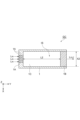
- FIG. 1 is an exploded perspective view of an atomic clock structure including a gas cell according to a first embodiment.
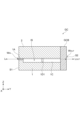
- FIG. 2 is a vertical cross-sectional view of the gas cell according to the first embodiment.
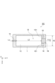
- FIG. 3 is a horizontal cross-sectional view of the gas cell according to the first embodiment.
- FIG. 4 is a diagram showing a vertical cross-sectional configuration of an atomic clock structure equipped with a heater.
- FIG. 5 is a diagram showing a vertical cross-sectional configuration of an atomic clock structure equipped with a heater.
- FIG. 6 is a diagram showing a vertical cross-sectional configuration of an atomic clock.
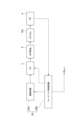
- FIG. 7 is a block diagram of an atomic clock.
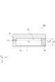
- FIG. 8 is a vertical cross-sectional view of a gas cell according to the second embodiment.
- FIG. 9 is a vertical cross-sectional view of a gas cell according to the third embodiment.
- FIG. 10 is a vertical cross-sectional view of a gas cell according to the fourth embodiment.
- FIG. 11 is a vertical cross-sectional view of a gas cell according to the fifth embodiment.
- FIG. 12 is a vertical cross-sectional view of a gas cell according to the sixth embodiment.
- FIG. 13 is a vertical cross-sectional view of a gas cell according to the seventh embodiment.
- FIG. 14 is a horizontal cross-sectional view of the gas cell.
- FIG. 15 is a horizontal cross-sectional view of the gas cell.
- FIG. 16 is a horizontal cross-sectional view of the gas cell.
- FIG. 17 is a horizontal cross-sectional view of the gas cell.
- FIG. 1 is an exploded perspective view of an atomic clock structure with a gas cell according to the first embodiment.
- the atomic clock structure 100 includes a gas cell GC, a laser element 3 optically coupled to a laser light inlet W IN of the gas cell GC, and a photodetector 4 optically coupled to an internal space IS (including the space in the first recess 1C) of the gas cell GC via a laser light outlet W OUT .
- a vertical cavity surface emitting laser (VCSEL) can be used as the laser element 3, and a photodiode can be used as the photodetector 4, but other types of elements may also be used.
- the optical component 5 is interposed between the gas cell GC and the laser element 3.
- the optical component 5 is one or more optical elements selected from a group of optical elements such as a lens, an optical filter, and a quarter-wave plate.
- the optical component 5 may include all of a lens, an optical filter, and a quarter-wave plate, and these optical elements may be arranged in order from the laser element 3 side toward the gas cell GC.
- the laser light introduced into the optical waveguide 1A travels in the Y-axis direction within the optical waveguide 1A and is emitted from the other end face of the optical waveguide 1A.
- the laser light emitted from the optical waveguide 1A is irradiated onto the gas in the internal space IS.
- This gas contains an alkali metal such as cesium (Cs) or rubidium (Rb). This gas may also contain a rare gas.
- this gas contains an alkali metal, absorption of the laser light occurs according to its energy level. By controlling the energy level and frequency of the laser light, the absorption rate of the laser light in the gas changes. If the control signal given to the laser element 3 is feedback-controlled so that it matches the specific energy level difference of the alkali atoms that make up the gas, the frequency (clock) of the output signal from the feedback control circuit will be an accurate value.
- the gas cell GC is provided with a first auxiliary space 1D and a second auxiliary space 1E that communicate with the internal space IS and in which some of the gas raw material in the internal space IS can remain. That is, a solid raw material containing an alkali metal is placed in advance in the first auxiliary space 1D and the second auxiliary space 1E. During production, when this solid raw material is heated and vaporized to be converted into gas in the internal space, some of the raw material (including impurities, etc.) may remain in the first auxiliary space 1D and the second auxiliary space 1E.
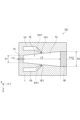
- FIG. 2 is a vertical cross-sectional view of a gas cell according to the first embodiment.
- An optical waveguide 1A is disposed on the first side S1 of the plate-shaped substrate.
- the optical waveguide 1A can be formed by etching the upper surface of the substrate 1 to form a groove, and then embedding a laser light transmitting material inside the groove.
- An example of a laser light transmitting material is glass (SiO 2 ).
- No optical waveguide is formed in the lid member 2. Except for the absence of an optical waveguide, the shape of the lid member 2 is the same as that of the substrate 1. That is, the lid member 2 has a first auxiliary space and a second auxiliary space having the same shapes as the first auxiliary space 1D and the second auxiliary space 1E shown in FIG. 1.
- the main space of the internal space IS of the gas cell GC is composed of a first recess 1C formed in the substrate 1 and a second recess 2C formed in the lid material 2.
- the depth direction of the first recess 1C is the negative direction of the Z axis
- the depth direction of the second recess 2C is the positive direction of the Z axis.
- the first recess 1C is connected to the first auxiliary space 1D via a first raw material gas inlet 1D1.
- the second recess 2C is connected to the first auxiliary space (not shown) of the lid material 2 via a second raw material gas inlet 2D1.
- the first recess 1C is connected to the second auxiliary space 1E (see FIG. 1) via a raw material gas inlet (not shown).
- the second recess 2C is connected to the second auxiliary space (not shown) of the lid material 2 via a raw material gas inlet (not shown).
- a first window material 1B is embedded in the area on the second side surface S2 side of the first recess 1C.
- a second window material 2B is embedded in the area on the second side surface S2 side of the second recess 2C.
- These window materials can be formed by embedding a laser light transmitting material in the area on the second side surface side of each recess after the formation of each recess.
- An example of a laser light transmitting material is glass (SiO 2 ). This may be formed by creating a block of the window material in a separate process and fixing the block in the area on the second side surface side of the recess.
- the dimension L1 in the thickness direction (Z-axis direction) of the internal space IS of the gas cell GC is set to be small.
- the optical path length L2 of the laser light traveling along the Y-axis within the internal space IS is greater than the dimension L1.
- the relationship of dimension L1 ⁇ optical path length L2 is satisfied.
- the optical path length L2 within the internal space IS is also the dimension of the internal space IS in the Y-axis direction.
- the laser light is reflected so that it travels back and forth inside the internal space IS along the Y-axis direction.
- the relationship L1 ⁇ L2 is satisfied.
- the angles of the walls at both ends in the Y-axis direction that define the internal space IS can be slightly inclined from the XZ plane, and a reflective film can be provided on these walls.
- the dimension L1 satisfies 0.1 ⁇ m ⁇ L1 ⁇ 1000 ⁇ m. If L1 is smaller than the lower limit, it becomes practically difficult to introduce laser light. If L1 exceeds the upper limit, the gas cell cannot be made sufficiently small. More preferably, the dimension L1 satisfies 1 ⁇ m ⁇ L1 ⁇ 500 ⁇ m. This gas cell GC is thinner than existing structures, so it can be installed in small devices such as mobile phones.
- the optical path length L2 (dimension) can be set, for example, to 100 ⁇ m ⁇ L2 ⁇ 5000 ⁇ m. If L2 is smaller than the lower limit, the amount of gas for the atomic clock will be insufficient. If L2 exceeds the upper limit, the gas cell cannot be made sufficiently small.
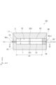
- FIG. 3 is a horizontal cross-sectional view of the gas cell according to the first embodiment. This figure is an XY cross-sectional view taken along the line indicated by the arrows III-III in FIG. 2.
- the first auxiliary space 1D and the second auxiliary space 1E are also located in the horizontal cross section of the substrate 1 where the internal space IS exists. Since the first auxiliary space 1D and the second auxiliary space 1E are formed from recesses, these recesses can be formed simultaneously when the first recess 1C is formed. The recesses can be formed by etching or the like.
- the horizontal cross-sectional shape of the optical waveguide 1A is rectangular.
- the optical waveguide 1A extends along the Y-axis direction.
- the XZ cross-sectional shape of the optical waveguide 1A is also rectangular, but it can also be a trapezoid or a triangle.
- a rectangle is an easy shape to process, and can also transmit laser light sufficiently.
- the horizontal cross-sectional shape of the internal space IS includes a trapezoid.
- the internal space IS has a second width X2 on the photodetector side that is wider than the first width X1 on the laser element side. Even if the laser light widens as it approaches the photodetector, it can still be adequately detected.
- the first raw material gas inlet 1D1 and the second raw material gas inlet 1E1 communicate with the hypotenuse of the trapezoidal internal space IS, and communicate with the first auxiliary space 1D and the second auxiliary space 1E, respectively.
- the shape of the first auxiliary space 1D is rectangular, and the direction of the first center line DX1 of the shape of the path from here to the first raw material gas inlet 1D1 is oriented in the direction of the XZ plane including the end face on the emission side of the gas cell.
- the shape of the second auxiliary space 1E is rectangular, and the direction of the second center line EX1 of the shape of the path from here to the second raw material gas inlet 1E1 is oriented in the direction of the XZ plane including the end face on the emission side of the gas cell. It is also possible to arrange the window material so that it is not located on the extension line of these center lines. Depending on the shape of the gas introduction path, it is also possible to suppress adhesion of raw materials to the optical waveguide and window material when introducing gas into the internal space.
- the shape of each auxiliary space can be set to a circle, ellipse, etc. instead of a rectangle.
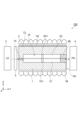
- Figure 4 shows the cross-sectional configuration of an atomic clock structure equipped with a heater.
- the atomic clock structure 100 includes a second heater H2 attached to the upper cover material 2 that constitutes a plate-shaped substrate.
- the atomic clock structure 100 includes a coil CL that surrounds the plate-shaped substrate (substrate 1 and cover material 2) along the Y-axis direction.
- the coil CL provides a static magnetic field inside the gas cell and suppresses the influence of external magnetic fields such as geomagnetism.
- the raw material can be vaporized by heating with the second heater H2.
- the second heater H2 can be used to control the gas pressure in the internal space IS if necessary, or to control the temperature of the laser element 3 arranged nearby.
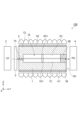
- Figure 5 shows the cross-sectional configuration of an atomic clock structure equipped with a heater.
- This atomic clock structure 100 has a structure in which a first heater H1 is further attached to the underside of the substrate 1 in the atomic clock structure 100 shown in FIG. 4.
- the first heater H1 can function in the same way as the second heater H2.
- Figure 6 shows the vertical cross-sectional structure of an atomic clock.
- the atomic clock 200 includes a wiring board 10, an atomic clock structure 100 mounted on the wiring board 10, and a control circuit 20 mounted on the wiring board 10.
- the control circuit 20 processes electrical signals in the atomic clock structure 100 and outputs a clock signal.
- the control circuit 20 can supply a drive signal to the laser element 3, receive a signal from the photodetector 4, generate a feedback signal from the received signal, and generate a drive signal for the laser element 3 from the feedback signal.
- the control circuit 20 can also control the power supplied to the first heater H1 and the second heater H2 based on the feedback signal or independently of the feedback signal.
- Figure 7 is a block diagram of an atomic clock.
- the control circuit 20 includes a drive circuit 20A that generates a drive signal (drive current) and a feedback control circuit 20B that receives the output signal of the photodetector 4 and performs feedback control of the drive signal.
- a laser light irradiation type atomic clock a laser light is irradiated onto a gas cell and output light from the gas cell is detected. The output light intensity changes due to the energy level transition of the gas.
- the output signal of the photodetector 4 is feedback controlled to generate a drive signal of a specific frequency so as to obtain a desired output light intensity that correlates with the energy level difference in the alkali atoms, and this frequency is used to measure time. The number of pulses contained in the signal of this frequency can also be measured and a clock signal S OUT can be output.
- the feedback control circuit 20B detects the level of the low-frequency component of the photodetector 4 and adjusts the frequency and amplitude of the drive signal output from the drive circuit 20A so that the detection level meets the target conditions.
- the feedback control circuit 20B can include a synchronous detection circuit to which the output signal of the photodetector 4 is input, a loop filter to which the error signal of the synchronous detection circuit is input, a local oscillator to which the control signal output from the loop filter is input, and a high-frequency synthesizer to which the output of the local oscillator is input.
- the drive signal output from the high-frequency synthesizer is input to the drive circuit 20A.
- the feedback control circuit 20B can also obtain an accurate frequency by utilizing the phenomenon of CPT (Coherent Population Trapping).
- CPT Cosmetic Population Trapping
- the drive signal modulates the output frequency of the laser element, and laser light of two sideband frequencies can be generated.
- the difference frequency of these sideband frequencies matches the transition frequency corresponding to a specific energy level difference of the alkali atom, CPT resonance occurs.
- the intensity of the transmitted light increases, so by monitoring the level of the low-frequency components of the photodetector 4, it is possible to obtain the frequency corresponding to a specific energy level difference of the atom.
- the wavelength of the laser light output from the laser element 3 can also be changed.
- the wavelength of the laser light can be controlled by the temperature generated by the laser element 3 by the drive signal itself, the temperature of the laser element 3 controlled by the power supplied to the heater, or the pressure applied to the laser element 3 when a piezoelectric element is attached to the laser element 3. Such control can be performed as necessary. Many types of control methods are known for atomic clocks, so an appropriate one can be adopted.
- FIG. 8 is a vertical cross-sectional view of a gas cell according to the second embodiment.
- This gas cell GC is the gas cell shown in Figure 2, in which the first window material 1B and the second window material 2B are integrated into one unit, forming the first window material 1B.
- This gas cell has the advantage of increasing light transmittance because there are no seams between the window materials.
- FIG. 9 is a vertical cross-sectional view of a gas cell according to the third embodiment.
- This gas cell GC is made by taking the first window material 1B from the gas cell shown in FIG. 8 out of the recess and attaching it as the third window material GCB to the light-emitting side surface of the substrate 1 and the lid material 2.
- This gas cell has the advantage of being easier to manufacture than the structure shown in FIG. 8.
- FIG. 10 is a vertical cross-sectional view of a gas cell according to the fourth embodiment.
- This gas cell GC is the gas cell shown in FIG. 9, with the lid 2 replaced by a simple plate. In other words, the bottom surface of the lid 2 is flat. This has the advantage that the lid 2 does not need to be processed.
- FIG. 11 is a vertical cross-sectional view of a gas cell according to the fifth embodiment.
- This gas cell GC is the gas cell shown in FIG. 10 with a thinner lid material 2.
- the thickness of the lid material 2 is smaller than the thickness of the substrate 1.
- FIG. 12 is a vertical cross-sectional view of a gas cell according to the sixth embodiment.
- This gas cell GC has the depth of the first recess 1C in the substrate 1 shown in FIG. 11 made the same as the depth of the optical waveguide 1A, and the thickness of the substrate 1 made thinner.
- This structure has the advantage of making the gas cell even smaller. It is also possible to omit the formation of the first recess 1C and instead place a frame-shaped plate material of the same thickness as the optical waveguide 1A between the substrate 1 and the lid material 2. If a deeper recess is required, it is also possible to adopt a structure in which a frame-shaped plate material is placed on the substrate 1, an optical waveguide and a window material are placed on top of that, a frame-shaped plate material is further laminated on top of that, and the lid material 2 is placed on top of that. In this structure, resin or glass may be interposed between the plates as necessary.
- FIG. 13 is a vertical cross-sectional view of a gas cell according to the seventh embodiment.
- This gas cell GC is formed by attaching a lid material 2 to the upper surface of a substrate 1 having a first recess 1C.
- the substrate 1 and the lid material 2 are made of a laser light transmitting material (SiO 2 ).
- the periphery of the gas cell can be covered with a light-shielding material. It is also possible to include a light-shielding material such as carbon in the area of the laser light transmitting material that does not transmit laser light.
- Figure 14 is a horizontal cross-sectional view of a gas cell.
- This gas cell has the horizontal cross-sectional shape of the internal space IS in the gas cell shown in Figure 3 modified from a trapezoid to a rectangle.
- the width of the internal space IS in the X-axis direction is constant (second width X2).
- This structure can increase the gas volume in the horizontal plane more than the structure in Figure 3.
- Figure 15 is a horizontal cross-sectional view of a gas cell.
- This gas cell is an example of the gas cell shown in FIG. 14, in which the position of the first auxiliary space 1D is set within the wall surface on the laser light incident side of the substrate 1.
- the first auxiliary space 1D is adjacent to the optical waveguide 1A.
- the first auxiliary space 1D is connected to the inside of the first recess 1C via the first raw material gas inlet 1D1.
- an auxiliary space and a raw material gas inlet connected thereto may be provided at a position in the lid material opposite the first auxiliary space 1D and the first raw material gas inlet 1D1.
- Figure 16 is a horizontal cross-sectional view of a gas cell.
- This gas cell is an example of the gas cell shown in FIG. 15, in which the second auxiliary space 1E is set in the wall surface on the laser light incident side of the substrate 1.
- the second auxiliary space 1E is adjacent to the optical waveguide 1A.
- the second auxiliary space 1E is connected to the inside of the first recess 1C via the second raw material gas inlet 1E1.
- an auxiliary space and a raw material gas inlet connected thereto may be provided in a position in the lid material opposite the second auxiliary space 1E and the second raw material gas inlet 1E1.
- Figure 17 shows a horizontal cross-sectional view of a gas cell.
- This gas cell is the gas cell shown in FIG. 15 with a plurality of first auxiliary spaces 1D, and each first auxiliary space 1D is connected to the first recess 1C via the first raw material gas inlet 1D1.
- the positions of these first auxiliary spaces 1D do not have to be on the same horizontal plane, and they may be distributed along the thickness direction.
- an auxiliary space and a raw material gas inlet connected thereto may be provided in a position in the lid opposite the first auxiliary space 1D and the first raw material gas inlet 1D1.
- the gas cell has a plurality of auxiliary spaces distributed, so it is also possible to increase the uniformity of the raw material gas flow when the gas is introduced.
- Figure 18 is a horizontal cross-sectional view of a gas cell.
- This gas cell is an example in which the positions of the first auxiliary space 1D and the second auxiliary space 1E in the gas cell shown in FIG. 16 are moved into the wall surface on the laser light emission side of the substrate 1.
- the first auxiliary space 1D is connected to the inside of the first recess 1C via the first raw material gas inlet 1D1.
- the second auxiliary space 1E is connected to the inside of the first recess 1C via the second raw material gas inlet 1E1.
- an auxiliary space and a raw material gas inlet connected thereto may be provided in a position in the lid material opposite the auxiliary space and raw material gas inlet formed in the substrate 1.
- This gas cell can obtain the same effect as the gas cell shown in FIG. 16.
- the shape of the auxiliary space in the horizontal plane is not limited to a circle, and various shapes such as an ellipse are possible.
- Figure 19 is a horizontal cross-sectional view of a gas cell.
- auxiliary space is not shown, but an auxiliary space as described above can be used.
- the gas cell of this example is an example in which the second width X2 of the internal space IS is set small in the gas cell of FIG. 14.
- the auxiliary space can also be provided within the wall surfaces located at both ends in the width direction. In this case, the gas cell can be made smaller.
- Figure 20 shows a horizontal cross-sectional view of a gas cell.
- the gas cell of this example is an example in which the longitudinal direction of the optical waveguide 1A is tilted with respect to the Y axis in the gas cell of FIG. 15.
- the second width X2 of the first window material 1B on the laser light emission side can be set to the second width X2 of the internal space IS.
- the optical path length L2 of the laser light traveling in the internal space IS can be set to be longer than the dimension of the internal space IS in the Y axis direction.
- the laser light in the internal space IS can be configured to be reflected by the inner wall surface of the substrate 1. A reflective film may be provided on this inner wall surface. In this case, the gas cell can be made smaller.
- Figure 21 shows a horizontal cross-sectional view of a gas cell.
- the gas cell of this example is an example of the gas cell of FIG. 20, in which multiple optical waveguides 1A are provided in the wall surface on the laser light incident side, and the longitudinal direction of each optical waveguide 1A is parallel to the Y axis. Since this structure has multiple optical waveguides 1A, it is possible to increase the amount of incident laser light.
- Figure 22 is a horizontal cross-sectional view of a gas cell.
- the auxiliary space is not shown, but an auxiliary space as described above can be used.
- the gas cell of this example is an example in which the position of the internal space IS is arranged asymmetrically with respect to the X-axis position of the optical waveguide 1A in the gas cell of FIG. 15. Even with this structure, it is possible to reduce the size of the gas cell.
- Figure 23 is a horizontal cross-sectional view of a gas cell.
- the gas cell of this example is an example in which the position of the first window material 1B in the gas cell shown in FIG. 15 is moved to the inside of the wall surface on the laser light incident surface side.
- a reflective film M1 may be provided on the inner wall surface located at the end of the Y-axis direction in the internal space IS. Examples of materials for the reflective film M1 include metals such as aluminum.
- the optical path length L2 of the laser light in the internal space IS becomes longer due to reflection, so the dimension of the gas cell in the Y-axis direction becomes smaller.
- the laser element and the photodetector are arranged adjacent to each other along the X-axis direction.
- the auxiliary space that serves as the source of gas raw material can have various positions, shapes, dimensions, and quantities as long as it is connected to the internal space, and is not limited to the above examples.
- the gas generated by decomposition of the raw material in the auxiliary space is supplied to the internal space.
- the substrate is equipped with an optical waveguide, but it is also possible to use a structure that does not have an optical waveguide and simply uses a through hole to introduce laser light.
- the above-mentioned gas cell and atomic clock structure can be miniaturized. If an atomic clock can be made sufficiently small, it will be possible to mount the atomic clock in a variety of devices.
- a miniaturized atomic clock can be mounted in a mobile phone, an automobile, a robot, a drone, a global positioning system (GPS), or a security system.
- GPS global positioning system
- REFERENCE SIGNS LIST 1 substrate, 1A: optical waveguide, 2: lid, 3: laser element, 4: photodetector, 100: atomic clock structure, GC: gas cell, IS: internal space, L IN , L OUT : laser light, W IN : laser light inlet, W OUT : laser light outlet.
Landscapes
- Physics & Mathematics (AREA)
- Spectroscopy & Molecular Physics (AREA)
- Investigating Or Analysing Materials By Optical Means (AREA)
Abstract
このガスセルGCは、ガスが充填された内部空間ISを有する板状の基板を備え、基板の第1側面S1に、内部空間ISに光学的に結合したレーザ光導入口WINを備えている。ガスセルGCは、基板の第1側面S1とは逆側の第2側面S2に、内部空間ISに光学的に結合したレーザ光出射口WOUTを備えている。ガスセルGCにおいて、内部空間ISにおける厚み方向の寸法L1と、厚み方向に垂直な平面内において、内部空間IS内を進行するレーザ光の光路長L2とは、L1<L2の関係を満たしている。
Description
本開示は、ガスセル及び原子時計用構造に関する。
原子時計は、正確な時間を計測する装置として知られている。原子時計には、幾つかの種類がある。近年では、CPT(Coherent Population Trapping)のように、ガスセル内のガスに、レーザ光を照射するタイプの原子時計が期待されている。ガスセル内には、ルビジウム(Rb)又はセシウム(Cs)などのアルカリ金属等を含むガスが封入される。計測方式としては、様々なタイプのものが考えられる。原子時計における物理的な構造部分、すなわち、レーザ素子、光検出器及びガスセルを備えた原子時計用構造についても、検討が行われている。特許文献1~特許文献3は、ガスセルを備えた原子時計を開示している。
ガスセル及びガスセルを備えた原子時計用構造の小型化が期待されている。
本開示のガスセルは、ガスが充填された内部空間を有する板状の基板を備え、基板の側面に、前記内部空間に光学的に結合したレーザ光導入口を備える。本開示のガスセルは、内部空間における厚み方向の寸法L1と、厚み方向に垂直な平面内において、内部空間内を進行するレーザ光の光路長L2とは、L1<L2の関係を満たす。原子時計用構造は、ガスセルと、前記レーザ光導入口に光学的に結合したレーザ素子と、前記内部空間に光学的に結合した光検出器とを備える。
以下、実施の形態に係るガスセル及び原子時計用構造について説明する。なお、同一要素には、同一符号を用いることとし、重複する説明は省略する。
図1は、第1実施形態に係るガスセルを備えた原子時計用構造の分解斜視図である。
原子時計用構造100は、ガスセルGCと、ガスセルGCのレーザ光導入口WINに光学的に結合したレーザ素子3と、ガスセルGCの内部空間IS(第1凹部1C内の空間を含む)に、レーザ光出射口WOUTを介して、光学的に結合した光検出器4とを備えている。レーザ素子3として垂直共振器型面発光レーザ(VCSEL)を用いることができ、光検出器4としてフォトダイオードを用いることができるが、別のタイプの素子を用いてもよい。
ガスセルGCと、レーザ素子3との間には、光学部品5が介在している。光学部品5は、レンズ、光学フィルタ及び1/4波長板などの光学要素群から選択される1個以上の光学要素である。光学部品5は、レンズ、光学フィルタ及び1/4波長板を全て備えていてもよく、これらの光学要素をレーザ素子3の側からガスセルGCに向けて、順番に並べて配置することもできる。
ガスセルGCは、ガスが充填された内部空間ISを有する板状の基板を備えている。板状の基板は、基板1と蓋材2を組み合わせてなる。説明においては、XYZ直交座標系を設定する。基板1の厚み方向をZ軸とし、基板1の長手方向をY軸とし、基板1の幅方向をX軸とし、これらの軸は、互いに直交している。板状の基板の第1側面S1には、この内部空間ISに光学的に結合したレーザ光導入口WINが設けられている。レーザ素子3から出射されたレーザ光LINは、Y軸方向に進行し、光学部品5を介して、レーザ光導入口WINに到達する。ガスセルGCは、レーザ光導入口WINと内部空間ISとの間に配置された光導波路1Aを備えている。レーザ光導入口WINは、光導波路1Aの一方の端面である。光導波路1Aは、Y軸に沿って延びている。
光導波路1A内に導入されたレーザ光は、光導波路1A内をY軸方向に進行して、光導波路1Aの他方の端面から出射される。光導波路1Aから出射したレーザ光は、内部空間IS内のガスに照射される。このガスは、セシウム(Cs)又はルビジウム(Rb)などのアルカリ金属を含むガスである。このガスは、希ガスを含むこともできる。
このガスが、アルカリ金属を含む場合、そのエネルギーレベルに応じて、レーザ光の吸収が生じる。レーザ光のエネルギーレベル及び周波数を制御することで、ガスにおけるレーザ光の吸収率が変化する。ガスを構成するアルカリ原子の特定のエネルギーレベル差に一致するように、レーザ素子3に与える制御信号をフィードバック制御すると、フィードバック制御回路からの出力信号の周波数(クロック)は、正確な値となる。
内部空間IS内をY軸方向に沿って進行し、これを通過したレーザ光は、第1窓材1Bの一方の端面に入射し、他方の端面(レーザ光出射口WOUT)から外部に出射される。換言すれば、ガスセルGCは、板状の基板の第1側面S1とは逆側の第2側面S2に、内部空間ISに光学的に結合したレーザ光出射口WOUTを備えている。レーザ光出射口WOUTから出射したレーザ光LOUTは、光検出器4に入射する。
ガスセルGCは、内部空間ISに連通し、内部空間IS内のガスの原料の一部が残留可能な第1補助空間1D及び第2補助空間1Eを備えている。すなわち、第1補助空間1D及び第2補助空間1E内には、予め、アルカリ金属を含む固体原料が配置されている。製造時において、この固体原料を加熱することで気化させ、内部空間内のガスに変換すると、第1補助空間1D及び第2補助空間1E内に原料の一部(不純物などを含む)が残留する場合がある。
ガスセルGCは、基板1の上面に固定された蓋材2を備えている。基板1の上面は、XY平面に平行である。蓋材2は、内部空間IS内を密閉状態とするために用いられる。蓋材2と基板1との間に接着剤を介在させることができる。基板1及び蓋材2の一方又は両方の材料は、それぞれ半導体又は金属とすることもできる。基板1及び蓋材2の一方又は両方の材料は、それぞれガラス又は樹脂とすることもできる。基板1及び蓋材2のいずれかの材料が、熱に対して溶ける材料であれば、これらの界面に熱と圧力を加えて、接着させることもできる。なお、本例の基板1の材料はシリコン(Si)であり、蓋材2の材料もシリコン(Si)であるとする。
図2は、第1実施形態に係るガスセルの縦断面図である。
板状の基板の第1側面S1側には、光導波路1Aが配置されている。光導波路1Aは、基板1の上面をエッチングして溝を形成した後、溝内部にレーザ光透過材料を埋め込むことで、形成することができる。レーザ光透過材料の一例はガラス(SiO2)である。蓋材2には、光導波路は形成されていない。光導波路が無い点を除いて、蓋材2の形状と、基板1の形状は同一である。すなわち、蓋材2は、図1に示した第1補助空間1D及び第2補助空間1Eと同一形状の第1補助空間及び第2補助空間を備えている。
ガスセルGCの内部空間ISの主要空間は、基板1に形成された第1凹部1Cと、蓋材2に形成された第2凹部2Cとから構成される。第1凹部1Cの深さ方向はZ軸の負方向であり、第2凹部2Cの深さ方向はZ軸の正方向である。第1凹部1Cは、第1原料ガス導入口1D1を介して、第1補助空間1Dに連通している。同様に、第2凹部2Cは、第2原料ガス導入口2D1を介して、蓋材2の第1補助空間(図示せず)に連通している。同様に、図示しない原料ガス導入口を介して、第1凹部1Cは、第2補助空間1E(図1参照)に連通している。同様に、図示しない原料ガス導入口を介して、第2凹部2Cは、蓋材2の第2補助空間(図示せず)に連通している。
第1凹部1Cの第2側面S2側の領域内には、第1窓材1Bが埋め込まれている。同様に、第2凹部2Cの第2側面S2側の領域内には、第2窓材2Bが埋め込まれている。これらの窓材は、それぞれの凹部の形成後に、その第2側面側の領域内に、レーザ光透過材料を埋め込むことで、形成することができる。レーザ光透過材料の一例はガラス(SiO2)である。窓材のブロックを別工程で作成しておき、凹部の第2側面側の領域内に、ブロックを固定することで、これを形成してもよい。
ガスセルGCの内部空間ISにおける厚み方向(Z軸方向)の寸法L1は、小さく設定されている。この厚み方向(Z軸方向)に垂直な平面(XY平面)内において、内部空間IS内を、Y軸に沿って進行するレーザ光の光路長L2は、寸法L1よりも大きい。すなわち、寸法L1<光路長L2の関係を満たしている。本例の内部空間IS内の光路長L2は、内部空間ISのY軸方向の寸法でもある。
レーザ光が、内部空間ISの内部をY軸方向に沿って往復するようにレーザ光を反射させる構造とすることも可能である。この構造においても、L1<L2の関係は満たされている。レーザ光を往復させるには、内部空間ISを規定するY軸方向両端の壁面の角度をXZ面から僅かに傾斜させ、これらの壁面に反射膜を設ければよい。
寸法L1は、0.1μm≦L1≦1000μmを満たしている。L1が、下限値よりも小さくなると、実質的にレーザ光を導入することが難しくなる。L1が、上限値を超えると、ガスセルを十分に小型化できない。寸法L1は、更に好ましくは1μm≦L1≦500μmを満たすことができる。このガスセルGCは、既存の構造よりも薄いので、携帯電話などの小型機器に搭載することも可能となる。
光路長L2(寸法)は、例えば、100μm≦L2≦5000μmに設定することができる。L2が、下限値よりも小さくなると、原子時計用のガス量が十分ではなくなる。L2が、上限値を超えると、ガスセルを十分に小型化できない。
図3は、第1実施形態に係るガスセルの水平断面図である。同図は、図2に示したIII-III矢印線に沿ったXY断面図である。
同図に示されるように、内部空間ISが存在する基板1の水平断面内において、第1補助空間1D及び第2補助空間1Eも位置している。第1補助空間1D及び第2補助空間1Eは凹部から形成されるので、これらの凹部は、第1凹部1Cの形成時に同時に形成することができる。凹部の形成方法としては、エッチング等を用いることができる。
光導波路1Aの水平断面形状は、長方形である。光導波路1AはY軸方向に沿って延びている。なお、光導波路1AのXZ断面の形状も長方形であるが、台形又は三角形とすることも可能である。なお、長方形は、加工しやすい形状であり、また、レーザ光を十分に伝達することもできる。
内部空間ISの水平断面形状は、台形を含んでいる。内部空間ISは、光検出器側の第2幅X2が、レーザ素子側の第1幅X1よりも広い。レーザ光が光検出器に向かうにしたがって広がっても、十分にレーザ光を検出することができる。
水平断面内において、台形の内部空間ISの斜辺には、第1原料ガス導入口1D1及び第2原料ガス導入口1E1が連通し、第1補助空間1D及び第2補助空間1Eにそれぞれ連通している。水平断面内において、第1補助空間1Dの形状を長方形とし、ここから第1原料ガス導入口1D1に至る経路の形状の第1中心線DX1の方向は、ガスセルの出射側の端面を含むXZ面の方向に向かっている。同様に、水平断面内において、第2補助空間1Eの形状を長方形とし、ここから第2原料ガス導入口1E1に至る経路の形状の第2中心線EX1の方向は、ガスセルの出射側の端面を含むXZ面の方向に向かっている。これらの中心線の延長線上に窓材が位置ないように配置することもできる。ガス導入経路の形状により、内部空間内へガス導入を行う場合の光導波路及び窓材への原料の付着を抑制することもできる。なお、各補助空間の形状は、長方形ではなく、円形又は楕円形等に設定することも可能である。
図4は、ヒータを備えた原子時計用構造の縦断面構成を示す図である。
同図では、構造を分かりやすく説明するために、レーザ素子3、光検出器4、光学部品5、ガスセルGCは、隙間を介して、示されている。これらの素子は、必要に応じて、密着させることもできる。原子時計用構造100は、板状の基板を構成する上部の蓋材2に取り付けられた第2ヒータH2を備えている。原子時計用構造100は、板状の基板(基板1及び蓋材2)をY軸方向に沿って囲むコイルCLを備えている。コイルCLは、ガスセル内部に静磁場を与えるものであり、地磁気等による外部磁場の影響を抑制している。第2ヒータH2による加熱により、原料を気化させることができる。その他、第2ヒータH2は、必要に応じて、内部空間IS内のガス圧力制御に用いることもでき、或いは、近接配置されたレーザ素子3の温度制御を行うことも可能である。
図5は、ヒータを備えた原子時計用構造の縦断面構成を示す図である。
この原子時計用構造100は、図4に示した原子時計用構造100における基板1の下面に、さらに第1ヒータH1を取り付けた構造を有している。第1ヒータH1は、第2ヒータH2と同様に機能させることができる。
図6は、原子時計の縦断面構成を示す図である。
原子時計200は、配線基板10と、配線基板10上に搭載された原子時計用構造100と、配線基板10上に搭載された制御回路20を備えている。制御回路20は、原子時計用構造100における電気信号を処理し、クロック信号を出力する。制御回路20は、レーザ素子3に駆動信号を供給し、光検出器4からの信号を受信し、受信した信号からフィードバック信号を生成し、フィードバック信号からレーザ素子3の駆動信号を生成することができる。制御回路20は、フィードバック信号に基づいて、或いは、フィードバック信号とは独立して、第1ヒータH1及び第2ヒータH2への供給電力を制御することもできる。
図7は、原子時計のブロック図である。
制御回路20は、駆動信号(駆動電流)を生成する駆動回路20Aと、光検出器4の出力信号を受信して、駆動信号のフィードバック制御を行うフィードバック制御回路20Bを備えている。レーザ光照射タイプの原子時計においては、レーザ光をガスセルに照射し、ガスセルからの出力光を検出する。ガスのエネルギーレベル遷移に起因して、出力光強度が変化する。原子時計においては、アルカリ原子におけるエネルギーレベル差に相関する目的の出力光強度が得られるように、光検出器4の出力信号をフィードバック制御して、特定の周波数の駆動信号を生成し、この周波数を利用して時間を計測している。この周波数の信号に含まれるパルス数を計測し、クロック信号SOUTを出力することもできる。
フィードバック制御回路20Bは、光検出器4の低周波成分のレベルを検出し、検出レベルが目的の条件を満たすように、駆動回路20Aから出力される駆動信号の周波数及び振幅を調整する。例えば、フィードバック制御回路20Bは、光検出器4の出力信号が入力される同期検波回路と、同期検波回路の誤差信号が入力されるループフィルタと、ループフィルタから出力される制御信号が入力される局部発振器と、局部発振器の出力が入力される高周波シンセサイザを備えることができる。高周波シンセサイザから出力された駆動信号は、駆動回路20Aに入力される。フィードバック制御回路20Bは、CPT(Coherent Population Trapping)の現象を利用して、正確な周波数を得ることもできる。この場合、駆動信号は、レーザ素子の出力周波数を変調するものであり、2つのサイドバンド周波数のレーザ光を発生させることができる。これらのサイドバンド周波数の差周波数が、アルカリ原子の特定のエネルギーレベル差に対応した遷移周波数に一致した場合、CPT共鳴が生じる。CPT共鳴時には、透過光強度が増加するので、光検出器4の低周波成分のレベルをモニタすれば、原子の特定のエネルギーレベル差に対応した周波数を得ることができる。
また、レーザ素子3から出力されるレーザ光の波長を変更することもできる。レーザ光の波長は、駆動信号自身によりレーザ素子3の発生する温度、ヒータへの供給電力により制御されるレーザ素子3の温度、又は、レーザ素子3に圧電素子を取り付けた場合にレーザ素子3に与えられる圧力などにより、制御することもできる。必要に応じて、このような制御を行うことも可能である。原子時計においては、数多くの種類の制御法が知られているので、適当なものを採用することができる。
図8は、第2実施形態に係るガスセルの縦断面図である。
このガスセルGCは、図2に示したガスセルにおける第1窓材1B及び第2窓材2Bを一体化し、一体化したものを第1窓材1Bとしたものである。このガスセルは、窓材の継ぎ目がないため、光透過率が増加するという利点がある。
図9は、第3実施形態に係るガスセルの縦断面図である。
このガスセルGCは、図8に示したガスセルにおける第1窓材1Bを、凹部内から取り出して、これを第3窓材GCBとして、基板1及び蓋材2の光出射面側の側面に貼り付けたものである。このガスセルは、図8の構造よりも、製造しやすいという利点がある。
図10は、第4実施形態に係るガスセルの縦断面図である。
このガスセルGCは、図9に示したガスセルの蓋材2を単なる板に変更したものである。すなわち、蓋材2の下面は、平坦面である。蓋材2を加工しないでよいという利点がある。
図11は、第5実施形態に係るガスセルの縦断面図である。
このガスセルGCは、図10に示したガスセルの蓋材2の厚みを薄くしたものである。すなわち、基板1の厚みよりも、蓋材2の厚みの方が小さい。この構造は、ガスセルをさらに小型化できるという利点がある。
図12は、第6実施形態に係るガスセルの縦断面図である。
このガスセルGCは、図11に示した基板1の第1凹部1Cの深さを、光導波路1Aの深さと同一とし、基板1の厚みを薄くしたものである。この構造は、ガスセルをさらに小型化できるという利点がある。なお、第1凹部1Cの形成を省略して、代わりに、光導波路1Aと同じ厚みの枠状の板材を、基板1と蓋材2との間に配置することもできる。なお、凹部の深さが必要な場合は、基板1上に枠状の板材を配置し、その上に光導波路と窓材を配置し、さらにその上に枠状の板材を積層し、その上に蓋材2を配置する構造を採用することもできる。この構造の場合、必要に応じて、板材間に樹脂又はガラスなどを介在させてもよい。
図13は、第7実施形態に係るガスセルの縦断面図である。
このガスセルGCは、第1凹部1Cを備えた基板1の上面に蓋材2を貼りつけたものである。基板1及び蓋材2は、レーザ光透過材料(SiO2)から構成されている。外部からの光を抑制するため、ガスセルの周囲を遮光材料で被覆することができる。また、レーザ光透過材料内において、レーザ光を透過させない領域内に、カーボン等の遮光材料を含有させることも可能である。
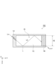
図14は、ガスセルの水平断面図である。
このガスセルは、図3に示したガスセルにおける内部空間ISの水平断面形状を、台形から長方形に変形したものである。すなわち、内部空間ISのX軸方向の幅が一定(第2幅X2)である。この構造は、図3の構造よりも、水平面内のガス容量を増加させることができる。
図15は、ガスセルの水平断面図である。
このガスセルは、図14に示したガスセルにおいて、第1補助空間1Dの位置を、基板1のレーザ光入射面側の壁面内に設定した例である。第1補助空間1Dは、光導波路1Aに隣接する。第1補助空間1Dは、第1原料ガス導入口1D1を介して、第1凹部1C内に連通している。上述の例と同様に、第1補助空間1D及び第1原料ガス導入口1D1に対向する蓋材内の位置に、補助空間及びこれに連通した原料ガス導入口を設けてもよい。この構造によれば、内部空間ISの第2幅X2の外側に位置する壁の厚さを薄くすることができ、さらなる小型化が可能である。
図16は、ガスセルの水平断面図である。
このガスセルは、図15に示したガスセルにおいて、第2補助空間1Eを、基板1のレーザ光入射面側の壁面内に設定した例である。第2補助空間1Eは、光導波路1Aに隣接する。第2補助空間1Eは、第2原料ガス導入口1E1を介して、第1凹部1C内に連通している。上述の例と同様に、第2補助空間1E及び第2原料ガス導入口1E1に対向する蓋材内の位置に、補助空間及びこれに連通した原料ガス導入口を設けてもよい。この構造によれば、ガスセルが複数の補助空間を備えているので、個々の補助空間の体積を小さくすることができ、光入射面側の壁面の厚さを小さくすることも可能であり、さらなる小型化が可能である。
図17は、ガスセルの水平断面図である。
このガスセルは、図15に示したガスセルにおいて、第1補助空間1Dの数を複数にしたものであり、個々の第1補助空間1Dは、それぞれ第1原料ガス導入口1D1を介して、第1凹部1C内に連通している。これらの第1補助空間1Dの位置は、同一の水平面内に無くてもよく、厚み方向に沿って分散して配置されていてもよい。上述の例と同様に、第1補助空間1D及び第1原料ガス導入口1D1に対向する蓋材内の位置に、補助空間及びこれに連通した原料ガス導入口を設けてもよい。この構造によれば、ガスセルが分散配置された複数の補助空間を備えているので、ガス導入時の原料ガス流の均一性を増加させることも可能である。
図18は、ガスセルの水平断面図である。
このガスセルは、図16に示したガスセルにおいて、第1補助空間1D及び第2補助空間1Eの位置を、基板1のレーザ光出射面側の壁面内に移動させた例である。第1補助空間1Dは、第1原料ガス導入口1D1を介して、第1凹部1C内に連通している。第2補助空間1Eは、第2原料ガス導入口1E1を介して、第1凹部1C内に連通している。上述の例と同様に、基板1に形成した補助空間及び原料ガス導入口に対向する蓋材内の位置に、補助空間及びこれに連通した原料ガス導入口を設けてもよい。このガスセルは、図16に示したガスセルと同様の効果を得ることができる。なお、補助空間の水平面内形状は、円形に限定されず、楕円形等の様々な形状とすることが可能である。
図19は、ガスセルの水平断面図である。
同図では、補助空間の図示を省略しているが、上述のような補助空間を採用することができる。本例のガスセルは、図14のガスセルにおいて、内部空間ISの第2幅X2を小さく設定した例である。補助空間は、幅方向両端に位置する壁面内に設けることも可能である。この場合、ガスセルを小型化することができる。
図20は、ガスセルの水平断面図である。
同図では、補助空間の図示を省略しているが、上述のような補助空間を採用することができる。本例のガスセルは、図15のガスセルにおいて、光導波路1Aの長手方向をY軸に対して傾斜させた例である。なお、レーザ光出射側の第1窓材1Bの第2幅X2は、内部空間ISの第2幅X2に設定することができる。このガスセルでは、内部空間IS内を進行するレーザ光の光路長L2を、内部空間ISのY軸方向の寸法よりも、長く設定することができる。内部空間IS内のレーザ光は、基板1の内壁面において反射される構成とすることができる。この内壁面上に反射膜を設けることとしてもよい。この場合、ガスセルを小型化することができる。
図21は、ガスセルの水平断面図である。
同図では、補助空間の図示を省略しているが、上述のような補助空間を採用することができる。本例のガスセルは、図20のガスセルにおいて、レーザ光入射面側の壁面内に複数の光導波路1Aを設け、各光導波路1Aの長手方向をY軸に平行とした場合の例である。この構造は、複数の光導波路1Aを備えているので、レーザ光の入射光量を増加させることができる。
図22は、ガスセルの水平断面図である。
同図では、補助空間の図示を省略しているが、上述のような補助空間を採用することができる。本例のガスセルは、図15のガスセルにおいて、内部空間ISの位置を光導波路1AのX軸方向位置に対して、非対称に配置した例である。この構造においても、ガスセルの小型化が可能である。
図23は、ガスセルの水平断面図である。
同図では、補助空間の図示を省略しているが、上述のような補助空間を採用することができる。本例のガスセルは、図15に示したガスセルにおける第1窓材1Bの位置を、レーザ光入射面側の壁面内に移動させた例である。内部空間IS内のY軸方向の端部に位置する内壁面上には、必要に応じて、反射膜M1を設けてもよい。反射膜M1の材料としては、アルミニウム等の金属が例示される。光導波路1Aから内部空間IS内に導入されたレーザ光は、反射膜M1により反射され、第1窓材1Bを介して外部に出力され、光検出器に導入される。レーザ光の内部空間IS内の光路長L2は、反射により長くなるので、ガスセルのY軸方向の寸法は小さくなる。なお、この構造においては、レーザ素子と光検出器は、X軸方向に沿って隣接して配置される。
上述のように、ガス原料の供給源となる補助空間は、内部空間内に連通していれば、その位置、形状、寸法、数量としては、様々な例を採用することができ、上述の例に限定されない。いずれの場合も、補助空間内において、原料分解により発生したガスは、内部空間内に供給される。なお、基板は光導波路を備えた方が好ましいが、光導波路を備えないで、単なる貫通孔を用いて、レーザ光を導入する構造も可能である。
以上、説明したように、上述のガスセル及び原子時計用構造は、小型化が可能である。原子時計を十分に小型化できると、様々な機器に、原子時計を搭載することが可能となる。例えば、携帯電話、自動車、ロボット、ドローン、全地球測位システム(GPS)、又は、セキュリティシステムなどに、小型化された原子時計を搭載することができる。
以上、種々の例示的実施形態について説明してきたが、上述した例示的実施形態に限定されることなく、様々な省略、置換、及び変更がなされてもよい。また、異なる実施形態における要素を組み合わせて他の実施形態を形成することが可能である。また、以上の説明から、本開示の種々の実施形態は、説明の目的本明細書において説明されており、本開示の範囲及び主旨から逸脱することなく種々の変更をなし得ることが、理解されるであろう。したがって、本明細書に開示した種々の実施形態は限定することを意図しておらず、真の範囲と主旨は、添付の特許請求の範囲によって示される。
1…基板、1A…光導波路、2…蓋材、3…レーザ素子、4…光検出器、100…原子時計用構造、GC…ガスセル、IS…内部空間、LIN,LOUT…レーザ光、WIN…レーザ光導入口、WOUT…レーザ光出射口。
Claims (13)
- ガスが充填された内部空間を有する板状の基板を備え、
前記基板の側面に、前記内部空間に光学的に結合したレーザ光導入口を備える、
ガスセル。 - 前記基板の前記側面とは逆側の側面に、前記内部空間に光学的に結合したレーザ光出射口を備える、
請求項1に記載のガスセル。 - 前記内部空間における厚み方向の寸法L1と、
前記厚み方向に垂直な平面内において、前記内部空間内を進行するレーザ光の光路長L2とは、
L1<L2の関係を満たす、
請求項1に記載のガスセル。 - 前記寸法L1は、0.1μm≦L1≦1000μmを満たす、
請求項3に記載のガスセル。 - 前記内部空間に連通し、前記ガスの原料の一部が残留可能な補助空間を有する、
請求項1に記載のガスセル。 - 前記内部空間が存在する前記基板の水平断面内において、前記補助空間も位置する、
請求項5に記載のガスセル。 - 前記ガスは、アルカリ金属を含む、
請求項1に記載のガスセル。 - 前記レーザ光導入口と前記内部空間との間に配置された光導波路備える、
請求項1に記載のガスセル。 - 前記光導波路の水平断面形状は、長方形である、
請求項8に記載のガスセル。 - 前記内部空間の水平断面形状は、台形を含む、
請求項1に記載のガスセル。 - 前記内部空間の水平断面形状は、長方形を含む、
請求項1に記載のガスセル。 - 前記基板に取り付けられたヒータを備える、
請求項1に記載のガスセル。 - 請求項1~請求項12のいずれか一項に記載のガスセルと、
前記レーザ光導入口に光学的に結合したレーザ素子と、
前記内部空間に光学的に結合した光検出器と、
を備える原子時計用構造。
Priority Applications (3)
| Application Number | Priority Date | Filing Date | Title |
|---|---|---|---|
| PCT/JP2023/024450 WO2025004352A1 (ja) | 2023-06-30 | 2023-06-30 | ガスセル及び原子時計用構造 |
| PCT/JP2024/013262 WO2025004484A1 (ja) | 2023-06-30 | 2024-03-29 | 原子時計用構造 |
| JP2025529453A JPWO2025004484A1 (ja) | 2023-06-30 | 2024-03-29 |
Applications Claiming Priority (1)
| Application Number | Priority Date | Filing Date | Title |
|---|---|---|---|
| PCT/JP2023/024450 WO2025004352A1 (ja) | 2023-06-30 | 2023-06-30 | ガスセル及び原子時計用構造 |
Publications (1)
| Publication Number | Publication Date |
|---|---|
| WO2025004352A1 true WO2025004352A1 (ja) | 2025-01-02 |
Family
ID=93938087
Family Applications (2)
| Application Number | Title | Priority Date | Filing Date |
|---|---|---|---|
| PCT/JP2023/024450 Ceased WO2025004352A1 (ja) | 2023-06-30 | 2023-06-30 | ガスセル及び原子時計用構造 |
| PCT/JP2024/013262 Ceased WO2025004484A1 (ja) | 2023-06-30 | 2024-03-29 | 原子時計用構造 |
Family Applications After (1)
| Application Number | Title | Priority Date | Filing Date |
|---|---|---|---|
| PCT/JP2024/013262 Ceased WO2025004484A1 (ja) | 2023-06-30 | 2024-03-29 | 原子時計用構造 |
Country Status (2)
| Country | Link |
|---|---|
| JP (1) | JPWO2025004484A1 (ja) |
| WO (2) | WO2025004352A1 (ja) |
Citations (6)
| Publication number | Priority date | Publication date | Assignee | Title |
|---|---|---|---|---|
| JPH02151122A (ja) * | 1988-12-02 | 1990-06-11 | Nippon Telegr & Teleph Corp <Ntt> | レーザ発振周波数安定化装置 |
| WO2014027637A1 (ja) * | 2012-08-17 | 2014-02-20 | 独立行政法人理化学研究所 | 光格子時計、時計装置、およびレーザー光源 |
| JP2018515012A (ja) * | 2015-03-31 | 2018-06-07 | 日本テキサス・インスツルメンツ株式会社 | 回転遷移ベースのクロック、回転分光セル、及びそれらの作成方法 |
| US20180366904A1 (en) * | 2015-05-07 | 2018-12-20 | Stc.Unm | Robust, compact, field-able tunable integrated photonic device |
| JP2020061451A (ja) * | 2018-10-10 | 2020-04-16 | 株式会社Usリサーチ | ガスセルおよびガスセルの製造方法 |
| JP2020123883A (ja) * | 2019-01-31 | 2020-08-13 | 国立研究開発法人情報通信研究機構 | 量子光学装置 |
Family Cites Families (4)
| Publication number | Priority date | Publication date | Assignee | Title |
|---|---|---|---|---|
| JP2017183377A (ja) * | 2016-03-29 | 2017-10-05 | セイコーエプソン株式会社 | 量子干渉装置、原子発振器、電子機器および移動体 |
| JP6838326B2 (ja) * | 2016-09-07 | 2021-03-03 | セイコーエプソン株式会社 | 発光素子モジュール、原子発振器、電子機器および移動体 |
| JP6741072B2 (ja) * | 2016-10-19 | 2020-08-19 | 株式会社村田製作所 | 原子発振器および電子機器 |
| JP7193079B2 (ja) * | 2018-10-16 | 2022-12-20 | 株式会社リコー | 原子発振器及び原子発振方法 |
-
2023
- 2023-06-30 WO PCT/JP2023/024450 patent/WO2025004352A1/ja not_active Ceased
-
2024
- 2024-03-29 WO PCT/JP2024/013262 patent/WO2025004484A1/ja not_active Ceased
- 2024-03-29 JP JP2025529453A patent/JPWO2025004484A1/ja active Pending
Patent Citations (6)
| Publication number | Priority date | Publication date | Assignee | Title |
|---|---|---|---|---|
| JPH02151122A (ja) * | 1988-12-02 | 1990-06-11 | Nippon Telegr & Teleph Corp <Ntt> | レーザ発振周波数安定化装置 |
| WO2014027637A1 (ja) * | 2012-08-17 | 2014-02-20 | 独立行政法人理化学研究所 | 光格子時計、時計装置、およびレーザー光源 |
| JP2018515012A (ja) * | 2015-03-31 | 2018-06-07 | 日本テキサス・インスツルメンツ株式会社 | 回転遷移ベースのクロック、回転分光セル、及びそれらの作成方法 |
| US20180366904A1 (en) * | 2015-05-07 | 2018-12-20 | Stc.Unm | Robust, compact, field-able tunable integrated photonic device |
| JP2020061451A (ja) * | 2018-10-10 | 2020-04-16 | 株式会社Usリサーチ | ガスセルおよびガスセルの製造方法 |
| JP2020123883A (ja) * | 2019-01-31 | 2020-08-13 | 国立研究開発法人情報通信研究機構 | 量子光学装置 |
Also Published As
| Publication number | Publication date |
|---|---|
| JPWO2025004484A1 (ja) | 2025-01-02 |
| WO2025004484A1 (ja) | 2025-01-02 |
Similar Documents
| Publication | Publication Date | Title |
|---|---|---|
| JP6354151B2 (ja) | 量子干渉装置、原子発振器、電子機器および移動体 | |
| US7999626B2 (en) | Physical section of atomic oscillator | |
| JP4292583B2 (ja) | 原子周波数取得装置および原子時計 | |
| JP6476751B2 (ja) | 原子セルの製造方法、原子セル、量子干渉装置、原子発振器および電子機器 | |
| JP6179327B2 (ja) | 量子干渉装置、原子発振器、電子機器および移動体 | |
| JP2015070331A (ja) | 原子セル、原子共鳴遷移装置、原子発振器、電子機器および移動体 | |
| JP4605508B2 (ja) | 原子周波数取得装置および原子時計 | |
| JP6435617B2 (ja) | 原子セル、量子干渉装置、原子発振器および電子機器 | |
| JP2015053304A (ja) | 原子セル、量子干渉装置、原子発振器、電子機器および移動体 | |
| US10756743B2 (en) | Atomic oscillator and electronic device | |
| CN105306054A (zh) | 原子室、量子干涉装置、原子振荡器、电子设备和移动体 | |
| JP6287169B2 (ja) | 量子干渉装置、原子発振器、電子機器および移動体 | |
| JP2015118962A (ja) | 量子干渉装置、原子発振器、電子機器および移動体 | |
| JP2015185911A (ja) | 原子セル、量子干渉装置、原子発振器、電子機器および移動体 | |
| JP6347101B2 (ja) | 量子干渉装置、原子発振器、電子機器および移動体 | |
| CN108628152B (zh) | 纳米y波导的芯片原子钟微型系统 | |
| JP5228275B2 (ja) | 原子周波数取得装置および原子時計 | |
| JP2017112515A (ja) | 原子発振器 | |
| JP2015115886A (ja) | 量子干渉装置、原子発振器、電子機器および移動体 | |
| JP7232510B2 (ja) | 量子光学装置 | |
| JP6337464B2 (ja) | 量子干渉装置、原子発振器、および電子機器 | |
| JP2016021455A (ja) | アルカリ金属セル及び原子発振器 | |
| US20150370222A1 (en) | Manufactureable long cell with enhanced sensitivity and good mechanical strength | |
| JP7319623B2 (ja) | 量子光学装置 | |
| JP2017220675A (ja) | 原子セルの製造方法、原子セル、量子干渉装置、原子発振器、電子機器および移動体 |
Legal Events
| Date | Code | Title | Description |
|---|---|---|---|
| 121 | Ep: the epo has been informed by wipo that ep was designated in this application |
Ref document number: 23943740 Country of ref document: EP Kind code of ref document: A1 |
|
| NENP | Non-entry into the national phase |
Ref country code: DE |