WO2024257416A1 - 外部電極形成装置及び外部電極形成方法 - Google Patents
外部電極形成装置及び外部電極形成方法 Download PDFInfo
- Publication number
- WO2024257416A1 WO2024257416A1 PCT/JP2024/007676 JP2024007676W WO2024257416A1 WO 2024257416 A1 WO2024257416 A1 WO 2024257416A1 JP 2024007676 W JP2024007676 W JP 2024007676W WO 2024257416 A1 WO2024257416 A1 WO 2024257416A1
- Authority
- WO
- WIPO (PCT)
- Prior art keywords
- paste
- filling hole
- element body
- paste filling
- conductive paste
- Prior art date
- Legal status (The legal status is an assumption and is not a legal conclusion. Google has not performed a legal analysis and makes no representation as to the accuracy of the status listed.)
- Ceased
Links
Images




Classifications
-
- H—ELECTRICITY
- H01—ELECTRIC ELEMENTS
- H01F—MAGNETS; INDUCTANCES; TRANSFORMERS; SELECTION OF MATERIALS FOR THEIR MAGNETIC PROPERTIES
- H01F41/00—Apparatus or processes specially adapted for manufacturing or assembling magnets, inductances or transformers; Apparatus or processes specially adapted for manufacturing materials characterised by their magnetic properties
- H01F41/02—Apparatus or processes specially adapted for manufacturing or assembling magnets, inductances or transformers; Apparatus or processes specially adapted for manufacturing materials characterised by their magnetic properties for manufacturing cores, coils, or magnets
- H01F41/04—Apparatus or processes specially adapted for manufacturing or assembling magnets, inductances or transformers; Apparatus or processes specially adapted for manufacturing materials characterised by their magnetic properties for manufacturing cores, coils, or magnets for manufacturing coils
-
- H—ELECTRICITY
- H01—ELECTRIC ELEMENTS
- H01F—MAGNETS; INDUCTANCES; TRANSFORMERS; SELECTION OF MATERIALS FOR THEIR MAGNETIC PROPERTIES
- H01F41/00—Apparatus or processes specially adapted for manufacturing or assembling magnets, inductances or transformers; Apparatus or processes specially adapted for manufacturing materials characterised by their magnetic properties
- H01F41/02—Apparatus or processes specially adapted for manufacturing or assembling magnets, inductances or transformers; Apparatus or processes specially adapted for manufacturing materials characterised by their magnetic properties for manufacturing cores, coils, or magnets
- H01F41/04—Apparatus or processes specially adapted for manufacturing or assembling magnets, inductances or transformers; Apparatus or processes specially adapted for manufacturing materials characterised by their magnetic properties for manufacturing cores, coils, or magnets for manufacturing coils
- H01F41/10—Connecting leads to windings
-
- H—ELECTRICITY
- H01—ELECTRIC ELEMENTS
- H01G—CAPACITORS; CAPACITORS, RECTIFIERS, DETECTORS, SWITCHING DEVICES, LIGHT-SENSITIVE OR TEMPERATURE-SENSITIVE DEVICES OF THE ELECTROLYTIC TYPE
- H01G13/00—Apparatus specially adapted for manufacturing capacitors; Processes specially adapted for manufacturing capacitors not provided for in groups H01G4/00 - H01G11/00
-
- H—ELECTRICITY
- H01—ELECTRIC ELEMENTS
- H01G—CAPACITORS; CAPACITORS, RECTIFIERS, DETECTORS, SWITCHING DEVICES, LIGHT-SENSITIVE OR TEMPERATURE-SENSITIVE DEVICES OF THE ELECTROLYTIC TYPE
- H01G4/00—Fixed capacitors; Processes of their manufacture
- H01G4/30—Stacked capacitors
Definitions
- This invention relates to an external electrode forming device and an external electrode forming method.
- Patent Document 1 discloses an external electrode forming device for forming external electrodes on the body of an electronic component.
- the external electrode forming device in Patent Document 1 has a casting table in which multiple bottomed paste filling holes are formed and the paste filling holes are filled with conductive paste. The body is moved until it contacts the bottom of the paste filling hole and is immersed in the conductive paste. This applies the conductive paste to the body.
- the element When applying conductive paste to the element as described above, the element may be immersed in the conductive paste in the paste filling hole with the center of the element misaligned with the center of the paste filling hole. If the element is immersed in the conductive paste in such an offset state, there may be variation in the length of the conductive paste applied to the element.
- the main object of the present invention is therefore to provide an external electrode forming device and method that can form external electrodes while suppressing variation in the length of conductive paste applied to the element body.
- the external electrode forming device includes a paste application table having a planar surface portion and at least one paste filling hole that is continuous with the surface portion and recessed relative to the upper surface of the surface portion, into which a portion of the base body of an electronic component is inserted.
- the paste application table is filled with a conductive paste for forming an external electrode on the base body, and the paste filling hole and the upper surface of the surface portion.
- conductive paste is filled not only in the paste filling holes, but also on the top surface of the flat portion adjacent to the paste filling holes. A part of the element body is inserted into the paste filling hole of the paste application table filled with conductive paste, and the conductive paste is applied to the element body.
- application length is the length from the end face of the element body to the end of the conductive paste, hereinafter also referred to simply as "application length" even if the element body is immersed in the paste filling hole with the center of the element body shifted from the center of the paste filling hole, and also makes it possible to suppress an increase in the standard deviation of the film thickness of the conductive paste on the end face of the element body.
- This invention provides an external electrode forming device and an external electrode forming method that can form external electrodes while suppressing variation in the length of conductive paste applied to the element body.
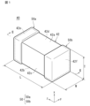
- 1 is an external perspective view showing an example of a coil component as an electronic component according to an embodiment
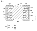
- 2 is a cross-sectional view of the coil component shown in FIG. 1 along line II-II.
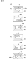
- FIG. 2 is an exploded plan view of the coil component shown in FIG. 1 .
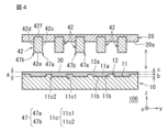
- 6 is a cross-sectional view of the external electrode forming apparatus according to the embodiment taken along line IV-IV in FIG. 5.
- 5 is a plan view of the external electrode forming apparatus shown in FIG. 4.
- 1A to 1C are cross-sectional views sequentially showing how a conductive paste is applied to an element body using a paste application table.
- 1 is a cross-sectional view showing a state in which an element body is immersed in conductive paste filled on a conventional paste application table.
- FIG. 10A to 10C are cross-sectional views showing aspects of an experiment according to a comparative example.
- 1A to 1D are cross-sectional views showing experimental aspects according to an embodiment of the present invention.
- FIG. 1 is a schematic diagram showing a method for measuring the standard deviation of film thickness and the difference in coating length on a WT cross section.
- 1A is a schematic diagram showing a state in which a conductive paste is filled on the top surface of a paste application table of a type of Comparative Example No.
- 1 having no paste filling hole, and an element body is immersed in the conductive paste and then lifted up
- (a) is a schematic diagram showing the state of application of the conductive paste and the state of air getting in
- (b) is a schematic diagram showing the conductive paste and the flow speed of the air by shading.
- 1A is a schematic diagram showing a state in which an element body is immersed in conductive paste and then pulled up in a paste application table of the type of Example No. 4 having a paste filling hole with conductive paste filling holes and flat portions
- (a) is a schematic diagram showing a state in which the conductive paste is applied and a state in which air has entered
- (b) is a schematic diagram showing the conductive paste and the flow speed of the air by shading.
- 13A and 13B are cross-sectional views showing modified examples of the side wall surface of a paste filling hole.
- 11A and 11B are cross-sectional views showing modified examples of the bottom surface of the paste filling hole.
- 13 is a plan view of a paste application table according to a modified example.
- Embodiment A coil component is used as an example of an electronic component according to an embodiment of the present invention, and an external electrode forming apparatus for applying a conductive paste to the body of the coil component will be described.
- Coil Component Fig. 1 is an external perspective view showing an example of a coil component as an electronic component according to an embodiment.
- Fig. 2 is a cross-sectional view of the coil component shown in Fig. 1 along line II-II.
- Fig. 3 is an exploded plan view of the coil component shown in Fig. 1.
- the coil component 40 includes an element body 42, a coil 44 provided inside the element body 42, and an external electrode 50 provided on the surface of the element body 42 and electrically connected to the coil 44.
- the element 42 is formed in a substantially rectangular parallelepiped shape.
- the element 42 has a first main surface 42a and a second main surface 42b facing each other in a height direction x (stacking direction), a first side surface 42c and a second side surface 42d facing each other in a width direction y perpendicular to the height direction x, and a first end surface 42e and a second end surface 42f facing each other in a length direction z perpendicular to the height direction x and the width direction y.
- the element 42 of this embodiment may have rounded corners and ridges.
- the corners refer to the portions where three adjacent surfaces of the element 42 intersect, and the ridges refer to the portions where two adjacent surfaces of the element 42 intersect.
- unevenness may be formed on a part or all of the first main surface 42a and the second main surface 42b, the first side surface 42c and the second side surface 42d, and the first end surface 42e and the second end surface 42f.
- the base body 42 includes a plurality of insulating layers 43.
- the plurality of insulating layers 43 are stacked in the height direction x.
- the insulating layers 43 are formed, for example, of a magnetic ferrite material.
- the magnetic ferrite material may include, for example, Fe2O3, ZnO, CuO, or NiO.
- the insulating layers 43 may further include additives such as, for example, Mn3O4, Co3O4, SnO2, Bi2O3, or SiO2.
- external electrodes 50 are disposed on the first end face 42e side and the second end face 42f side of the element body 42.
- the external electrode 50 has a first external electrode 50a and a second external electrode 50b.
- the first external electrode 50a is disposed on at least the surface of the first end face 42e.
- the first external electrode 50a extends from the first end face 42e and is disposed on a portion of the first main face 42a and a portion of the second main face 42b, as well as a portion of the first side face 42c and a portion of the second side face 42d.
- the second external electrode 50b is disposed on at least the surface of the second end face 42f.
- the second external electrode 50b extends from the second end face 42f and is disposed on a portion of the first main face 42a and a portion of the second main face 42b, as well as a portion of the first side face 42c and a portion of the second side face 42d.
- the coil 44 is wound in a spiral shape along the height direction x.
- the coil 44 is made of a conductive material such as Ag or Cu.
- the coil 44 has a plurality of coil conductors 44a, a first connecting conductor 44b, and a second connecting conductor 44c.
- the first connecting conductor 44b, the plurality of coil conductors 44a, and the second connecting conductor 44c are arranged in order along the height direction x and are electrically connected in order through via conductors.
- the plurality of coil conductors 44a are connected in order along the height direction x to form a spiral shape along the height direction x.
- the first connecting conductor 44b is exposed from the first end surface 42e of the element body 42 and connected to the first external electrode 50a.
- the second connecting conductor 44c is exposed from the second end surface 42f of the element body 42 and connected to the second external electrode 50b.
- Fig. 4 is a cross-sectional view of the external electrode forming apparatus according to one embodiment taken along line IV-IV in Fig. 5.
- Fig. 5 is a plan view of the external electrode forming apparatus shown in Fig. 4.
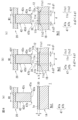
- Figs. 6(a) to 6(c) are cross-sectional views sequentially showing how a conductive paste is applied to an element body using a paste application table.
- the external electrode forming apparatus 100 includes a paste application table 10 filled with a conductive paste 30 for forming an external electrode 50.
- the external electrode forming apparatus 100 of this embodiment includes a holding device 20 for raising and lowering the element body 42 of the coil component 40 relative to the paste application table 10.
- the paste application table 10 has a plurality of paste filling holes 11 and a plurality of flat portions 12.
- the flat portions 12 are formed in a flat shape and have upper surfaces 12a facing upward.
- the paste filling holes 11 are formed between adjacent flat portions 12, so as to be continuous with the flat portions 12 and to be recessed with respect to the upper surfaces 12a of the flat portions 12.
- the paste filling holes 11 are formed so that a part of the element body 42 can be inserted therein.
- the paste filling holes 11 are formed in a rectangular shape in a cross-sectional view as shown in FIG. 4, and have a flat bottom surface 11a and a pair of flat side wall surfaces 11b rising vertically upward from the ends of the bottom surface 11a.
- the paste filling holes 11 are formed so as to extend long along the height direction x (predetermined direction) of the coil component 40 as shown in the plan view of FIG. 5, and are formed so that a plurality of element bodies 42 can be inserted in parallel in the height direction x of the coil component 40.
- the number of paste filling holes 11 is not limited as long as it is one or more.
- the paste application table 10 is arranged with the bottom surface 11a of the paste filling hole 11 and the top surface 12a of the flat surface 12 facing upward.
- the paste application table 10 is prepared with the conductive paste 30 filled not only in the paste filling hole 11 but also on the top surface 12a of the flat surface 12.
- the paste thickness a of the conductive paste 30 is the thickness of the conductive paste 30 from the bottom surface 11a of the paste filling hole 11.
- the paste thickness a is the sum of the depth b of the paste filling hole 11 and the thickness c of the conductive paste 30 on the top surface 12a of the flat surface 12.
- the element body 42 When applying the conductive paste 30 to the element body 42, the element body 42 is lowered toward the paste filling hole 11 until it contacts the bottom surface 11a of the paste filling hole 11, so that a part of the element body 42 is immersed in the conductive paste 30. As shown in Figures 5 and 6 (a), such a paste filling hole 11 is formed so that the length d of the paste filling hole 11 in the width direction y of the coil component 40 is greater than the length f (W dimension in this embodiment) of the element body 42 in the width direction y.
- the paste filling hole 11 is preferably formed so that when the element body 42 is inserted into the paste filling hole 11, the distance between the element body end 47 of the element body 42 and the hole end 11c of the paste filling hole 11 is 10 ⁇ m or more and 1000 ⁇ m or less.
- the first distance ⁇ g1 between the first element body end 47a on the first side surface 42c side of the element body 42 and the first hole end 11c1 of the paste filling hole 11 is preferably 10 ⁇ m or more and 1000 ⁇ m or less.
- the second distance ⁇ g2 between the second element body end 47b on the second side surface 42d side of the element body 42 and the second hole end 11c2 of the paste filling hole 11 is preferably 10 ⁇ m or more and 1000 ⁇ m or less.
- the length h of the upper surface 12a of the planar portion 12 in the width direction y is the length in the width direction y between adjacent paste filling holes 11. It is preferable that this length h is designed so that the conductive paste 30 that spills out of the paste filling hole 11 onto the upper surface 12a of the planar portion 12 can be extended in a generally planar shape by immersing the element 42 in the paste filling hole 11 as shown in FIG. 6(a). It is preferable that the length h is, for example, at least half the length d (1/2d) and at most d.
- c/a which is the ratio of thickness c to paste thickness a
- c/a is 0.2 or more.
- the conductive paste 30 contains a metal component.
- the metal component contains at least one selected from, for example, Ag, Au, Cu, Ni, Pd, Sn, Bi, or an alloy containing them.
- the reason for using Ag as the metal component is that Ag has the lowest resistivity among metals, making it suitable as an electrode material, and Ag is a precious metal, so it does not oxidize and has high weather resistance.
- Metal powder with Ag coating on the surface of the metal powder can also be used as the metal component. When using metal powder with Ag coating on the surface, it is preferable to use Cu, Ni, Sn, Bi, or an alloy powder of these.
- the reason for using Ag-coated metal powder is that it is possible to make the base metal cheaper while maintaining the above-mentioned characteristics of Ag.
- the conductive paste 30 can contain a glass component in addition to the metal component.
- the glass component contains at least one selected from B, Si, Ba, Mg, Al, Li, etc.
- a conductive resin paste can be used as the conductive paste 30.
- the conductive resin paste contains, for example, a thermosetting resin and a metal component.
- the metal component is the same as described above.
- thermosetting resin various known thermosetting resins such as epoxy resin, phenoxy resin, phenol resin, urethane resin, silicone resin, and polyimide resin can be used.
- the conductive paste 30 has a viscosity of 10 Pa ⁇ s or more and 60 Pa ⁇ s or less, a density of 2000 kg/m3 or more and 3000 kg/m3 or less, and a surface tension of 0.01 N/m or more and 0.04 N/m or less.
- the holding device 20 holds the element body 42 so that the element body 42 can be inserted into the paste filling hole 11 of the paste application table 10.
- the holding device 20 is arranged so that its lower surface 20a faces the surface of the paste application table 10 on which the paste filling hole 11 is formed.
- the holding device 20 holds the element body 42 in a state in which a part of the element body 42 protrudes from the lower surface 20a at a position on the lower surface 20a facing the paste filling hole 11.
- the holding device 20 holds the element body 42 in a state in which the entire first end surface 42e, a part of the first side surface 42c, a part of the second side surface 42d, a part of the first main surface 42a, and a part of the second main surface 42b are exposed from the lower surface 20a.
- the first end surface 42e faces downward so as to face the paste filling hole 11.
- the number of element bodies 42 held by the holding device 20 is not limited, and may be one or more.
- the holding device 20 of this embodiment holds two or more element bodies 42 .
- the paste application table 10 is prepared with the conductive paste 30 filled not only in the paste filling holes 11 but also on the top surface 12a of the flat portion 12.
- the holding device 20 holds a number of element bodies 42 so that the first end faces 42e face the paste filling holes 11, and lowers the element bodies 42 towards the paste application table 10.
- the first end face 42e of the element body 42 comes into contact with the bottom face 11a of the paste filling hole 11 or is lowered close to the bottom face, and a part of the element body 42 is immersed in the conductive paste 30.
- the conductive paste 30 overflows from the paste filling hole 11 by the volume of the element body 42.
- the paste thickness of the conductive paste 30 increases by ⁇ a, to a + ⁇ a. It is considered that the overflowing conductive paste 30 is pulled by the conductive paste 30 on the upper face 12a of the flat portion 12 and extends in a generally planar manner on the upper face 12a of the flat portion 12. This prevents the overflowing conductive paste 30 from being applied to the element body 42 in a raised state.
- the holding device 20 raises the element body 42 from the paste filling hole 11 while the conductive paste 30 is applied to the element body 42.
- the amount of conductive paste 30 in the paste filling hole 11 is reduced by the amount of conductive paste 30 adhering to the element body 42.
- the conductive paste 30 filling the upper surface 12a of the flat portion 12 is drawn from the upper surface 12a of the flat portion 12 into the paste filling hole 11.
- the conductive paste 30 applied to the element body 42 is pulled by the conductive paste 30 drawn from the upper surface 12a of the flat portion 12 into the paste filling hole 11, forming an extended portion 30a.
- the holding device 20 further raises the element body 42 out of the paste filling hole 11, and separates the element body 42 from the conductive paste 30 on the paste application table 10.
- the conductive paste 30 is applied to the first end face 42e, part of the first main surface 42a, part of the second main surface 42b, part of the first side surface 42c, and part of the second side surface 42d of the element body 42.
- the element body 42 is held by the holding device 20 so that the second end face 42f faces the paste application table 10.
- the element body 42 is immersed in the conductive paste 30 on the paste application table 10, so that the conductive paste 30 is applied to the second end face 42f, a portion of the first main surface 42a, a portion of the second main surface 42b, a portion of the first side surface 42c, and a portion of the second side surface 42d.
- the element 42 is fired at a temperature of about 800°C with the conductive paste 30 applied to the first end face 42e, the second end face 42f, part of the first main face 42a, part of the second main face 42b, part of the first side face 42c, and part of the second side face 42d.
- the first external electrode 50a and the second external electrode 50b including the base electrode layer and the plating layer made of the conductive paste 30 may be formed by forming a plating layer such as a Ni plating layer and a Sn plating layer on the fired conductive paste 30.
- the conductive paste 30 is filled not only in the paste filling holes 11 but also on the upper surface 12a of the planar portion 12 continuous with the paste filling holes 11.
- a part of the element body 42 is inserted into the paste filling holes 11 of the paste application table 10 in a state where the conductive paste 30 is filled, and the conductive paste 30 is applied to the element body 42.
- the application length is application length e1 from the left end of the first end face 42e of the element 42 to the end of the conductive paste 30, and application length e2 from the right end of the first end face 42e of the element 42 to the end of the conductive paste 30.
- Figure 7 is a cross-sectional view showing the state in which the element is immersed in the conductive paste filled in a conventional paste coating table.
- the conductive paste 30 When the element 42 is inserted into the paste filling hole 11, as shown in FIG. 6(a), the conductive paste 30 overflows from the paste filling hole 11 by the volume of the element 42. It is considered that the overflowing conductive paste 30 is pulled by the conductive paste 30 on the upper surface 12a of the flat portion 12 and extends in a generally planar manner on the upper surface 12a of the flat portion 12. This prevents the overflowing conductive paste 30 from being applied to the element 42 in a raised state.
- the conventional paste application table 1B has a paste filling hole 11 and a flat surface 12 formed thereon, similar to the paste application table 10 according to this embodiment.
- the paste filling hole 11 is filled with conductive paste 30
- the upper surface 12a of the flat surface 12 is not filled with conductive paste 30.
- the conductive paste 30 overflows from the paste filling hole 11 onto the upper surface 12a of the flat surface 12 by the volume of the element 42, and the overflowing conductive paste 30 forms a raised portion 31 on the surface of the element 42 due to surface tension.
- the shape of the raised portion 31 will differ depending on the surface position of the element 42.
- the conductive paste 30 that has overflowed from the paste filling hole 11 is prevented from being applied to the element body 42 in a mounded state as shown in FIG. 6(a), so that even if the element body 42 is inserted with its center offset from the center of the paste filling hole 11, variation in the application length of the conductive paste 30 on the element body 42 can be suppressed.
- the conductive paste 30 in the paste filling hole 11 is applied to the element body 42.
- the element body 42 is pulled up from the paste filling hole 11 with the conductive paste 30 applied.
- the conductive paste 30 filled on the upper surface 12a of the flat portion 12 is drawn from the upper surface 12a of the flat portion 12 into the paste filling hole 11 as the conductive paste 30 is pulled up together with the element body 42.
- the conductive paste 30 applied to the element body 42 is pulled by the conductive paste 30 drawn from the upper surface 12a of the flat portion 12 into the paste filling hole 11, so that the extension portion 30a of the conductive paste 30 extending from the first end surface 42e (second end surface 42f) of the element body 42 toward the paste filling hole 11 becomes thinner.
- the absolute amount of conductive paste 30 applied to the element 42 can be reduced compared to when the conductive paste 30 is filled in the paste application table 10 without the paste filling hole 11. This also narrows the extension portion 30a of the conductive paste 30 extending from the first end face 42e (second end face 42f) of the element 42 toward the paste filling hole 11.
- the amount of conductive paste 30 applied to the first end face 42e (second end face 42f) of the element 42 can be reduced, and the standard deviation of the film thickness of the conductive paste 30 at the first end face 42e (second end face 42f) of the element 42 can be reduced from increasing. It is considered that an air flow flows toward the extension portion 30a between the conductive paste 30 applied to the element 42 with the extension portion 30a and the conductive paste 30 drawn into the paste filling hole 11 from the upper surface 12a of the flat portion 12. It is considered that the extension portion 30a also narrows due to this air flow.
- the distance between the element body end 47 of the element body 42 and the hole end 11c of the paste filling hole 11 is formed to be 10 ⁇ m or more and 1000 ⁇ m or less, it is possible to suppress the variation in the application length and the increase in the standard deviation of the film thickness. Specifically, when the distance between the element body 42 and the paste filling hole 11 is 10 ⁇ m or more and the paste filling hole 11 becomes large, the ratio of the volume of the element body 42 to the amount of conductive paste 30 in the paste filling hole 11 becomes small. Therefore, when the element body 42 is inserted into the paste filling hole 11, the amount of conductive paste 30 that overflows becomes smaller than the amount of conductive paste 30 in the paste filling hole 11.
- the overflowing conductive paste 30 is extended in a generally planar shape. Therefore, the conductive paste 30 overflowing from the paste filling hole 11 is prevented from being applied to the element body 42 in a raised state, so that even if the element body 42 is inserted with its center offset from the center of the paste filling hole 11, the variation in the application length of the conductive paste 30 on the element body 42 can be suppressed. Furthermore, because the raised state of the conductive paste 30 is suppressed, it is also possible to suppress the conductive paste 30 from being applied in a state that deviates from the required application length.
- the distance between the element body 42 and the paste filling hole 11 is 1000 ⁇ m or less, the absolute amount of conductive paste 30 applied to the element body 42 can be reduced. Therefore, when the element body 42 is pulled up from the paste filling hole 11 with the conductive paste 30 applied, the extension portion 30a extending from the first end face 42e (second end face 42f) of the element body 42 toward the paste filling hole 11 becomes thinner. Therefore, the amount of conductive paste 30 applied to the first end face 42e (second end face 42f) of the element body 42 can be reduced, and the standard deviation of the film thickness of the conductive paste 30 at the first end face 42e (second end face 42f) of the element body 42 can be reduced.
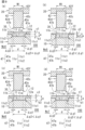
- FIGS. 8(a) to (c) are cross-sectional views showing an embodiment of an experiment according to a comparative example.
- FIGS. 9(a) to (d) are cross-sectional views showing an embodiment of an experiment according to an embodiment of the present invention.
- comparative examples experiments were performed in the modes of comparative examples No. 1 to No. 3 in FIGS. 8(a) to (c), respectively.
- embodiments experiments were performed in the modes of embodiments No. 4 to No. 7 in FIGS. 9(a) to (d), respectively.
- the conductive paste used had a viscosity of 50 Pa ⁇ s, a density of 2700 kg/m3, and a surface tension of 0.02 N/m.
- FIG. 8(a) An experiment was carried out using a conventional external electrode forming apparatus 1.
- the paste application table 1A of the conventional external electrode forming apparatus 1 does not have a paste filling hole 11, unlike the paste application table 10 according to the present embodiment.
- the holding device 20 is the same as that of the present embodiment, and holds an element 42.
- the holding device 20 was lowered, so that the element 42 was immersed in the conductive paste 30 on the paste application table 1A.
- the holding device 20 was then raised, so that an element 42 coated with the conductive paste 30 was obtained.
- the upper surface 12a of the flat portion 12 was not filled with conductive paste 30, and the paste applying table 1B was prepared in a state in which only the paste filling hole 11 was filled with conductive paste 30.
- the paste thickness a was 230 ⁇ m.
- the holding device 20 held the element body 42 so that the center of the element body 42 coincided with the center of the paste filling hole 11.
- the first distance ⁇ g1 between the first element body end 47a on the first side surface 42c side of the element body 42 and the first hole end 11c1 of the paste filling hole 11 was 200 ⁇ m
- the holding device 20 was moved up and down to obtain an element body 42 on which the conductive paste 30 was applied.
- Example No. 5 An experiment was carried out using the external electrode forming device 100 according to the present embodiment.
- the paste thickness a was 230 ⁇ m.
- the holding device 20 held the element body 42 in a state in which the center of the element body 42 was shifted from the center of the paste filling hole 11.
- the first distance ⁇ g1 was 300 ⁇ m
- the second distance ⁇ g2 was 100 ⁇ m ( ⁇ g1> ⁇ g2).
- the holding device 20 was moved up and down to obtain an element body 42 coated with the conductive paste 30.
- Example No. 6 An experiment was carried out using the external electrode forming device 100 according to the present embodiment.
- the paste thickness a was 230 ⁇ m.
- the holding device 20 held the element body 42 in a state in which the center of the element body 42 was shifted from the center of the paste filling hole 11.
- the first distance ⁇ g1 was 300 ⁇ m
- the second distance ⁇ g2 was 100 ⁇ m ( ⁇ g1> ⁇ g2).
- the holding device 20 was moved up and down to obtain an element body 42 coated with the conductive paste 30.
- Example No. 7 An experiment was conducted using the external electrode forming device 100 according to the present embodiment.
- the paste thickness a was 230 ⁇ m.
- the holding device 20 held the element body 42 in a state in which the center of the element body 42 was shifted from the center of the paste filling hole 11.
- the first distance ⁇ g1 was 300 ⁇ m
- the second distance ⁇ g2 was 100 ⁇ m ( ⁇ g1 > ⁇ g2).
- the element body 42 coated with the conductive paste 30 was obtained by moving the holding device 20 up and down.
- FIG. 10 is a schematic diagram showing a method for measuring the film thickness standard deviation and the difference in application length in the WT cross section.
- FIG. 10 shows the end of the element body 42 on the first end face 42e side to which the conductive paste 30 is applied.
- the film thickness standard deviation was obtained at the first end face 42e.
- the end face smooth portion is the portion from position P1 to position P13.
- the interval between adjacent positions P1 to P13 is 5 mm.
- the film thickness of the conductive paste 30 at each of positions P1 to P13 in this end face smooth portion was obtained.
- the film thickness of the conductive paste 30 was obtained as a length t8 from the end of the conductive paste 30 hanging down from the first end face 42e to the first end face 42e.
- a film thickness standard deviation which is an index of film thickness variation, was obtained based on the film thickness of the conductive paste 30 at each of positions P1 to P13.
- Table 1 shows the results for c/a, paste shape at the end surface, standard deviation of film thickness, and difference in application length for No. 1 to No. 7.
- FIG. 11 is a schematic diagram showing a state in which the element body is immersed in the conductive paste and then pulled up in a state in which the conductive paste is filled on the top surface of the paste coating table of Comparative Example No. 1 type that does not have a paste filling hole, (a) is a schematic diagram showing the coating state of the conductive paste and the intrusion state of air, and (b) is a schematic diagram showing the conductive paste and the flow rate of the air in shading.
- the extension portion 30a of the conductive paste 30 extending from the first end surface 42e of the element body 42 toward the top surface 1a of the paste coating table 1A is formed over the entire first end surface 42e and has become thick.
- FIG. 11(b) although there is a flow of air 60 flowing toward the extension portion 30a between the conductive paste 30 applied to the base body 42 with the extension portion 30a and the conductive paste 30 drawn into the paste filling hole 11 from the upper surface 12a of the planar portion 12, the extension portion 30a has become thicker as described above.
- the paste application table 1B has a paste filling hole 11, and only the paste filling hole 11 is filled with the conductive paste 30.
- the film thickness standard deviation in Comparative Example No. 2 was smaller than that in Example No. 4, in which the paste filling hole 11 and the flat portion 12 of the paste application table 10 according to the present embodiment are filled with the conductive paste 30.
- the difference in the application length was suppressed to 1 ⁇ m or less.
- the paste application table 1B of Comparative Example No. 2 was used and the element body 42 was immersed in the conductive paste 30 with the center of the element body 42 shifted from the center of the paste filling hole 11 as in Comparative Example No. 3, the difference in the application length was large, reaching 184 ⁇ m.
- the film thickness standard deviation in Comparative Example No. 3 was approximately the same as that in Example No. 4 according to the present embodiment. Therefore, if only the paste filling hole 11 is filled with the conductive paste 30 and the flat surface portion 12 is not filled with the conductive paste 30, it was found that if the element 42 is immersed in the conductive paste 30 and pulled up with the center of the element 42 misaligned with the center of the paste filling hole 11, it is not possible to simultaneously suppress both the variation in the coating length and the increase in the standard deviation of the film thickness.
- the standard deviation of the film thickness in Example No. 4 is smaller than that in Comparative Example No. 1, and the difference in the application length is suppressed to 1 ⁇ m or less.
- FIG. 12 is a schematic diagram showing the state in which the paste filling hole and the plane portion are filled with conductive paste in the paste application table of Example No.
- the extension 30a of the conductive paste 30 extending from the first end surface 42e of the element body 42 toward the bottom surface 11a of the paste filling hole 11 is smaller than the first end surface 42e and is thinner. This is thought to be because the extension 30a is pulled by the conductive paste 30 drawn from the upper surface 12a of the flat portion 12 into the paste filling hole 11, and the absolute amount of the conductive paste 30 is reduced by being restricted by the paste filling hole 11.
- the amount of air 60 flowing toward the extension 30a increases and the flow rate of the air 60 is faster than in FIG. 11(b), which is thought to make the extension 30a thinner. Therefore, it is possible to suppress the amount of conductive paste 30 applied to the first end surface 42e of the element body 42, and it is thought that it is possible to suppress the increase in the standard deviation of the film thickness of the conductive paste 30 at the first end surface 42e of the element body 42.
- the difference in application length was 15 ⁇ m, which was smaller than the difference in application length of 184 ⁇ m in Comparative Example No. 3.
- the standard deviation of the film thickness in Example No. 7 was smaller than that in Comparative Example No. 1.
- the difference in application length was 26 ⁇ m, which was smaller than the difference in application length of 184 ⁇ m in Comparative Example No. 3.
- the standard deviation of film thickness in Example No. 5 was smaller than that in Comparative Example No. 1.
- the difference in application length was 23 ⁇ m, which was smaller than the difference in application length of 184 ⁇ m in Comparative Example No. 3.
- the standard deviation of film thickness in Example No. 6 was smaller than that of Comparative Example No. 1.
- c/a is preferably 0.13 or more. Furthermore, c/a is more preferably 0.345 or more. When c/a is in this range, the variation in the application length can be suppressed to a desired range, and the standard deviation of the film thickness of the conductive paste 30 on the first end surface 42e of the element body 42 can be suppressed to a desired range.
- the sidewall surface 11b of the paste filling hole 11 is formed in a flat shape rising vertically upward from the end of the bottom surface 11a.
- the shape of the sidewall surface 11b is not limited to this, and may be formed to chamfer the corners of the paste filling hole 11.
- Figures 13(a) and (b) are cross-sectional views showing modified sidewall surfaces of the paste filling hole.
- the sidewall surface 11b may be formed by an inclined surface that inclines outward from the end of the bottom surface 11a upward as shown in Figure 13(a).
- the sidewall surface 11b may be formed to have a curved surface that curves outward from the end of the bottom surface 11a upward as shown in Figure 13(b).
- the sidewall surface 11b may be formed to have a curved surface that curves inward from the end of the bottom surface 11a upward.
- the above configuration can further suppress the increase in the standard deviation of the film thickness of the conductive paste 30 on the first end face 42e (second end face 42f) of the element body 42, and can reduce the difference in the application length.
- a flow of air 60 flows toward the extension portion 30a between the conductive paste 30 applied to the element body 42 with the extension portion 30a and the conductive paste 30 drawn into the paste filling hole 11 from the upper surface 12a of the flat portion 12. It is considered that the flow rate of this air 60 is increased by at least a part of the side wall surface 11b of the paste filling hole 11 being formed into a curved or inclined surface.
- the increased flow rate of the air 60 makes the extension portion 30a even thinner, and the amount of conductive paste 30 applied to the first end face 42e (second end face 42f) of the element body 42 can be suppressed. This suppresses the increase in the standard deviation of the film thickness, and can reduce the difference in the application length.
- Fig. 14 is a cross-sectional view showing a modified example of the bottom surface of the paste filling hole.
- the bottom surface 11a may be formed with a bottom surface uneven portion 11a1 having an uneven shape with respect to the bottom surface 11a.
- the above configuration can further suppress the increase in the standard deviation of the film thickness of the conductive paste 30 at the first end face 42e (second end face 42f) of the element 42, and can reduce the difference in the application length.
- air bubbles may enter the extension portion 30a of the conductive paste 30 extending from the first end face 42e (second end face 42f) of the element 42 toward the paste filling hole 11, causing the extension portion 30a to become thicker.
- the bottom surface uneven portion 11a1 on the bottom surface 11a of the paste filling hole 11 as described above, it is thought that air bubbles are captured by the bottom surface uneven portion 11a1.
- the extension portion 30a becomes thinner, and the amount of conductive paste 30 applied to the first end face 42e (second end face 42f) of the element 42 can be suppressed.
- the paste filling hole 11 becomes smaller by the amount of the bottom surface unevenness 11a1, so the absolute amount of conductive paste 30 applied to the element body 42 can be reduced.
- This also makes the extension portion 30a thinner. This prevents the standard deviation of the film thickness from becoming too large, and reduces the difference in application length.
- the planar shape of the paste filling hole 11 is formed to extend long along the height direction x of the coil component 40 as shown in Fig. 5.
- the shape of the paste filling hole 11 is not limited to this.
- Fig. 15 is a plan view of a paste application table according to a modified example.
- the paste filling hole 11 is formed such that when one element body 42 is inserted into the paste filling hole 11, the side wall surface of one paste filling hole 11 surrounds one element body 42.
- the adhesive force of the conductive paste 30 becomes approximately uniform around the entire circumference of the element body 42. Therefore, it is possible to suppress the variation in the applied length of the conductive paste 30 around the entire circumference of the element body 42. Furthermore, when the element body 42 is pulled up from the paste filling hole 11 with the conductive paste 30 applied, the conductive paste 30 applied to the element body 42 is pulled from the entire circumference of the element body 42 by the conductive paste 30 drawn into the paste filling hole 11 from the upper surface 12a of the planar portion 12.
- the extension portion 30a of the conductive paste 30 extending from the first end face 42e (second end face 42f) of the element body 42 toward the paste filling hole 11 becomes even thinner. Therefore, it is possible to suppress the increase in the standard deviation of the film thickness of the conductive paste 30 at the first end face 42e (second end face 42f) of the element body 42.
- the first distance ⁇ g1 between the first element end 47a on the first side surface 42c side of the element body 42 and the first hole end 11c1 of the paste filling hole 11 is 10 ⁇ m or more and 1000 ⁇ m or less. It is also preferable that the second distance ⁇ g2 between the second element end 47b on the second side surface 42d side of the element body 42 and the second hole end 11c2 of the paste filling hole 11 is 10 ⁇ m or more and 1000 ⁇ m or less. It is also preferable that the third distance ⁇ g3 between the third element end 47c on the first main surface 42a side of the element body 42 and the third hole end 11c3 of the paste filling hole 11 is 10 ⁇ m or more and 1000 ⁇ m or less. In addition, the fourth distance ⁇ g4 between the fourth element body end 47d on the second main surface 42b side of the element body 42 and the fourth hole end 11c4 of the paste filling hole 11 is preferably 10 ⁇ m or more and 1000 ⁇ m or less.
- the external electrode forming apparatus 100 of the above embodiment includes a holding device 20.
- the holding device 20 may be omitted.
- the coil component 40 may be manually immersed in the conductive paste 30 on the paste application table 10.
- the coil component 40 may be manually immersed in a state in which the coil component 40 is attached to an adhesive sheet or the like.
- the paste application table 10 may be moved up and down from below the coil component 40 with respect to the coil component 40 in a state in which the coil component 40 is attached to the top surface with an adhesive sheet or the like and arranged.
- the coil component 40 has been given as an example of an electronic component.
- electronic components to which the present invention can be applied are not limited to the coil component 40, and may include, for example, a capacitor, an all-solid-state battery, a piezoelectric component, a thermistor element, and the like.
- the electronic component When a dielectric material is used for the insulating layer 43, the electronic component functions as a capacitor.
- the dielectric material include dielectric ceramics containing components such as BaTiO3, CaTiO3, SrTiO3, and CaZrO3.
- a subcomponent such as a Mn compound, an Fe compound, a Cr compound, a Co compound, or a Ni compound may be added in a smaller amount than the main component depending on the desired characteristics of the element body 42.
- the electronic component functions as a piezoelectric component when a piezoelectric ceramic material is used for the insulating layer 43.
- the piezoelectric ceramic material examples include PZT (lead zirconate titanate) based ceramic materials.
- the electronic component functions as a thermistor element when a semiconductor ceramic material is used for the insulating layer 43.
- Specific examples of the semiconductor ceramic material include spinel ceramic materials.
- a paste applying table having a flat surface portion and at least one paste filling hole formed therein, the paste filling hole being continuous with the flat surface portion and recessed with respect to an upper surface of the flat surface portion, and into which a part of an element body of an electronic component is inserted; an external electrode forming apparatus, wherein the paste applying table is filled with a conductive paste for forming external electrodes on the element body, the paste filling holes and the upper surface of the flat portion.
- ⁇ 2> The external electrode forming apparatus described in ⁇ 1>, wherein the paste filling hole is formed so that the distance between the element body end of the element body inserted into the paste filling hole and the hole end of the paste filling hole adjacent to the element body end is 10 ⁇ m or more and 1000 ⁇ m or less.
- ⁇ 4> 4 The external electrode forming apparatus according to any one of ⁇ 1> to ⁇ 3>, wherein a ratio of a thickness of the conductive paste on the flat portion to a thickness of the conductive paste in the paste filling hole is 0.2 or more.
- ⁇ 5> The external electrode forming apparatus according to any one of ⁇ 1> to ⁇ 4>, wherein at least a part of a side wall surface of the paste filling hole is formed into a curved or inclined surface.
- ⁇ 6> The external electrode forming apparatus according to any one of ⁇ 1> to ⁇ 5>, wherein a bottom surface uneven portion having an uneven shape relative to the bottom surface of the paste filling hole is formed on the bottom surface of the paste filling hole.
- ⁇ 7> The external electrode forming apparatus according to any one of ⁇ 1> to ⁇ 6>, wherein the conductive paste contains at least one of silver, gold, and copper.
- a method for forming external electrodes using an external electrode forming apparatus comprising: a paste application table having a planar portion and at least one paste filling hole formed therein, the paste filling hole being continuous with the planar portion and recessed with respect to an upper surface of the planar portion, into which a part of an element body of an electronic component is inserted; and the paste application table is filled with a conductive paste for forming an external electrode on the element body, the paste filling hole and an upper surface of the planar portion, dipping at least one of the bodies into the conductive paste by lowering the body toward the paste filling hole; and lifting the element body with the conductive paste applied thereto out of the paste filling hole.
- ⁇ 11> The method for forming an external electrode according to any one of ⁇ 8> to ⁇ 10>, wherein a ratio of a thickness of the conductive paste on the flat portion to a thickness of the conductive paste in the paste filling hole is 0.2 or more.
- ⁇ 12> The method for forming an external electrode according to any one of ⁇ 8> to ⁇ 11>, wherein at least a part of a side wall surface of the paste filling hole is formed into a curved or inclined surface.
- ⁇ 14> The method for forming an external electrode according to any one of ⁇ 8> to ⁇ 13>, wherein the conductive paste contains at least one of silver, gold, and copper.
Landscapes
- Engineering & Computer Science (AREA)
- Power Engineering (AREA)
- Manufacturing & Machinery (AREA)
- Microelectronics & Electronic Packaging (AREA)
- Fixed Capacitors And Capacitor Manufacturing Machines (AREA)
Abstract
素体における導電性ペーストの塗布長さのばらつきを抑制した状態で外部電極を形成可能な外部電極形成装置を提供する。外部電極形成装置100は、平面状の平面部12と、平面部12に連続するとともに平面部12の上面12aに対して凹んでおり、電子部品の素体42の一部が挿入される少なくとも1つのペースト充填穴11と、が形成されているペースト塗布用テーブル10を備え、ペースト塗布用テーブル10には、素体42に外部電極50を形成するための導電性ペースト30がペースト充填穴11及び平面部12の上面12aに充填されている。
Description
この発明は、外部電極形成装置及び外部電極形成方法に関する。
特許文献1には、電子部品の素体に外部電極を形成するための外部電極形成装置が開示されている。特許文献1の外部電極形成装置は、複数の有底のペースト充填穴が形成され、そのペースト充填穴に導電性ペーストが充填されたキャスティングテーブルを有する。素体をペースト充填穴の底面に接するまで移動し、導電性ペーストに浸漬する。これにより、素体に導電性ペーストが塗布される。
上述のように素体に導電性ペーストを塗布する際に、ペースト充填穴の中心に対して素体の中心がずれた状態で素体がペースト充填穴内の導電性ペーストに浸漬される場合がある。このようにずれた状態で導電性ペーストに素体が浸漬されると、素体に塗布された導電性ペーストの塗布長さにばらつきが生じてしまう場合がある。
それゆえに、この発明の主たる目的は、素体における導電性ペーストの塗布長さのばらつきを抑制した状態で外部電極を形成可能な外部電極形成装置及び外部電極形成方法を提供することである。
この発明に係る外部電極形成装置は、平面状の平面部と、平面部に連続するとともに平面部の上面に対して凹んでおり、電子部品の素体の一部が挿入される少なくとも1つのペースト充填穴と、が形成されているペースト塗布用テーブルを備え、ペースト塗布用テーブルには、素体に外部電極を形成するための導電性ペーストがペースト充填穴及び平面部の上面に充填されている。
上記のペースト塗布用テーブルには、ペースト充填穴だけでなく、ペースト充填穴に連続する平面部の上面にも導電性ペーストが充填されている。導電性ペーストが充填された状態のペースト塗布用テーブルのペースト充填穴に素体の一部を挿入して素体に導電性ペーストを塗布する。これにより、ペースト充填穴の中心に対して素体の中心がずれた状態で素体がペースト充填穴に浸漬されても、素体に塗布された導電性ペーストの塗布長さ(塗布長さは、素体の端面から導電性ペーストの端部までの長さであり、以下、単に「塗布長さ」ともという。)のばらつきを抑制することができるとともに、素体の端面における導電性ペーストの膜厚標準偏差が大きくなることを抑制することができる。
この発明によれば、素体における導電性ペーストの塗布長さのばらつきを抑制した状態で外部電極を形成可能な外部電極形成装置及び外部電極形成方法を提供することができる。
この発明の上述の目的、その他の目的、特徴及び利点は、図面を参照して行う以下の発明を実施するための形態の説明から一層明らかとなろう。
1.実施の形態
この発明の実施の形態にかかる電子部品の例としてコイル部品を用い、このコイル部品の素体に導電性ペーストを塗布するための外部電極形成装置について説明する。
この発明の実施の形態にかかる電子部品の例としてコイル部品を用い、このコイル部品の素体に導電性ペーストを塗布するための外部電極形成装置について説明する。
(1)コイル部品
図1は、実施の形態にかかる電子部品としてのコイル部品の一例を示す外観斜視図である。図2は、図1に示すコイル部品の線II-II断面図である。図3は、図1に示すコイル部品の分解平面図である。コイル部品40は、素体42と、素体42の内部に設けられているコイル44と、素体42の表面に設けられてコイル44と電気的に接続されている外部電極50と、を備える。
図1は、実施の形態にかかる電子部品としてのコイル部品の一例を示す外観斜視図である。図2は、図1に示すコイル部品の線II-II断面図である。図3は、図1に示すコイル部品の分解平面図である。コイル部品40は、素体42と、素体42の内部に設けられているコイル44と、素体42の表面に設けられてコイル44と電気的に接続されている外部電極50と、を備える。
(1-1)素体
素体42は、略直方体状に形成されている。素体42は、高さ方向x(積層方向)に相対する第1の主面42a及び第2の主面42bと、高さ方向xに直交する幅方向yに相対する第1の側面42c及び第2の側面42dと、高さ方向x及び幅方向yに直交する長さ方向zに相対する第1の端面42e及び第2の端面42fとを有する。本実施の形態の素体42には、角部及び稜線部に丸みがつけられていてもよい。なお、角部とは、素体42の隣接する3面が交わる部分のことであり、稜線部とは、素体42の隣接する2面が交わる部分のことである。また、第1の主面42a及び第2の主面42b、第1の側面42c及び第2の側面42d、ならびに第1の端面42e及び第2の端面42fの一部又は全部に凹凸などが形成されていてもよい。
素体42は、略直方体状に形成されている。素体42は、高さ方向x(積層方向)に相対する第1の主面42a及び第2の主面42bと、高さ方向xに直交する幅方向yに相対する第1の側面42c及び第2の側面42dと、高さ方向x及び幅方向yに直交する長さ方向zに相対する第1の端面42e及び第2の端面42fとを有する。本実施の形態の素体42には、角部及び稜線部に丸みがつけられていてもよい。なお、角部とは、素体42の隣接する3面が交わる部分のことであり、稜線部とは、素体42の隣接する2面が交わる部分のことである。また、第1の主面42a及び第2の主面42b、第1の側面42c及び第2の側面42d、ならびに第1の端面42e及び第2の端面42fの一部又は全部に凹凸などが形成されていてもよい。
素体42は、複数の絶縁層43を含む。複数の絶縁層43は高さ方向xに積層される。絶縁層43は例えば磁性フェライト材料によって形成される。磁性フェライト材料は、例えば、Fe2O3、ZnO、CuO又はNiOを含むことができる。絶縁層43は、例えばMn3O4、Co3O4、SnO2、Bi2O3又はSiO2等の添加剤をさらに含み得る。
(1-2)外部電極
素体42の第1の端面42e側及び第2の端面42f側には、図1、図2に示されるように、外部電極50が配置される。
素体42の第1の端面42e側及び第2の端面42f側には、図1、図2に示されるように、外部電極50が配置される。
外部電極50は、第1の外部電極50a及び第2の外部電極50bを有する。
第1の外部電極50aは、少なくとも第1の端面42eの表面に配置されている。本実施の形態では、第1の外部電極50aは、第1の端面42eから延伸して第1の主面42aの一部及び第2の主面42bの一部、ならびに第1の側面42cの一部及び第2の側面42dの一部にも配置される。
第2の外部電極50bは、少なくとも第2の端面42fの表面に配置されている。本実施の形態では、第2の外部電極50bは、第2の端面42fから延伸して第1の主面42aの一部及び第2の主面42bの一部、ならびに第1の側面42cの一部及び第2の側面42dの一部にも配置される。
(1-3)コイル
コイル44は、高さ方向xに沿って螺旋状に巻回されている。コイル44は、例えばAgまたはCu等の導電性材料からなる。コイル44は、複数のコイル導体44aと、第1の接続導体44bと、第2の接続導体44cと、を有する。第1の接続導体44bと、複数のコイル導体44aと、第2の接続導体44cとは、高さ方向xに沿って順に配置され、ビア導体を介して電気的に順に接続される。複数のコイル導体44aは、高さ方向xに沿って順に接続されて高さ方向xに沿った螺旋状を形成する。第1の接続導体44bは、素体42の第1の端面42eから露出して第1の外部電極50aに接続されている。第2の接続導体44cは、素体42の第2の端面42fから露出して第2の外部電極50bに接続されている。
コイル44は、高さ方向xに沿って螺旋状に巻回されている。コイル44は、例えばAgまたはCu等の導電性材料からなる。コイル44は、複数のコイル導体44aと、第1の接続導体44bと、第2の接続導体44cと、を有する。第1の接続導体44bと、複数のコイル導体44aと、第2の接続導体44cとは、高さ方向xに沿って順に配置され、ビア導体を介して電気的に順に接続される。複数のコイル導体44aは、高さ方向xに沿って順に接続されて高さ方向xに沿った螺旋状を形成する。第1の接続導体44bは、素体42の第1の端面42eから露出して第1の外部電極50aに接続されている。第2の接続導体44cは、素体42の第2の端面42fから露出して第2の外部電極50bに接続されている。
(2)外部電極形成装置
次に、外部電極形成装置100について説明する。図4は、一実施の形態に係る外部電極形成装置の図5の線IV-IV断面図である。図5は、図4に示す外部電極形成装置の平面図である。図6(a)~(c)は、ペースト塗布用テーブルを用いて素体に導電性ペーストが塗布されている様子を順に示す断面図である。外部電極形成装置100は、外部電極50を形成するための導電性ペースト30が充填されているペースト塗布用テーブル10を備える。さらに、本実施の形態の外部電極形成装置100は、ペースト塗布用テーブル10に対してコイル部品40の素体42を上下させるための保持装置20を備える。
次に、外部電極形成装置100について説明する。図4は、一実施の形態に係る外部電極形成装置の図5の線IV-IV断面図である。図5は、図4に示す外部電極形成装置の平面図である。図6(a)~(c)は、ペースト塗布用テーブルを用いて素体に導電性ペーストが塗布されている様子を順に示す断面図である。外部電極形成装置100は、外部電極50を形成するための導電性ペースト30が充填されているペースト塗布用テーブル10を備える。さらに、本実施の形態の外部電極形成装置100は、ペースト塗布用テーブル10に対してコイル部品40の素体42を上下させるための保持装置20を備える。
(2-1)ペースト塗布用テーブル
ペースト塗布用テーブル10は、複数のペースト充填穴11と複数の平面部12とが形成されている。平面部12は平面状に形成されており、上方に向いた上面12aを有する。ペースト充填穴11は、互いに隣接する平面部12の間において、当該平面部12に連続するとともに平面部12の上面12aに対して凹んで形成されている。また、ペースト充填穴11は素体42の一部が挿入可能なように形成されている。本実施の形態では、ペースト充填穴11は、図4に示すように断面視において長方形状に形成されており、平面状の底面11aと、底面11aの端部から鉛直方向に上方に立ち上がる平面状の一対の側壁面11bと、を有する。また、本実施の形態では、ペースト充填穴11は、図5の平面図に示すように、コイル部品40の高さ方向x(所定方向)に沿って長く延びるように形成されており、複数の素体42をコイル部品40の高さ方向xに並列させて挿入可能なように形成されている。なお、ペースト充填穴11の数は1つ以上あればよく、数は限定されない。
ペースト塗布用テーブル10は、複数のペースト充填穴11と複数の平面部12とが形成されている。平面部12は平面状に形成されており、上方に向いた上面12aを有する。ペースト充填穴11は、互いに隣接する平面部12の間において、当該平面部12に連続するとともに平面部12の上面12aに対して凹んで形成されている。また、ペースト充填穴11は素体42の一部が挿入可能なように形成されている。本実施の形態では、ペースト充填穴11は、図4に示すように断面視において長方形状に形成されており、平面状の底面11aと、底面11aの端部から鉛直方向に上方に立ち上がる平面状の一対の側壁面11bと、を有する。また、本実施の形態では、ペースト充填穴11は、図5の平面図に示すように、コイル部品40の高さ方向x(所定方向)に沿って長く延びるように形成されており、複数の素体42をコイル部品40の高さ方向xに並列させて挿入可能なように形成されている。なお、ペースト充填穴11の数は1つ以上あればよく、数は限定されない。
外部電極形成装置100においては、ペースト充填穴11の底面11a及び平面部12の上面12aが上方に向く状態でペースト塗布用テーブル10が配置されている。そして、ペースト充填穴11だけでなく平面部12の上面12aにも導電性ペースト30が充填された状態でペースト塗布用テーブル10が準備される。このとき、導電性ペースト30のペースト厚aは、ペースト充填穴11の底面11aからの導電性ペースト30の厚みである。ペースト厚aは、ペースト充填穴11の深さbと平面部12の上面12aにおける導電性ペースト30の厚みcとを足した値となっている。
素体42に導電性ペースト30を塗布する場合、素体42がペースト充填穴11の底面11aに接触するまでペースト充填穴11に向けて下降されることにより、素体42の一部が導電性ペースト30に浸漬される。このようなペースト充填穴11は、図5及び図6(a)に示すように、コイル部品40の幅方向yにおけるペースト充填穴11の長さdが幅方向yにおける素体42の長さf(本実施の形態ではW寸法)よりも大きくなるように形成される。具体的に、ペースト充填穴11は、ペースト充填穴11に素体42が挿入された状態で、素体42の素体端部47とペースト充填穴11の穴端部11cとの距離が10μm以上1000μm以下となるように形成されていることが好ましい。つまり、素体42における第1の側面42c側の第1の素体端部47aとペースト充填穴11の第1の穴端部11c1との間の第1の距離Δg1は、10μm以上1000μm以下であることが好ましい。また、素体42における第2の側面42d側の第2の素体端部47bとペースト充填穴11の第2の穴端部11c2との間の第2の距離Δg2は、10μm以上1000μm以下であることが好ましい。
また、幅方向yにおける平面部12の上面12aの長さhは、隣接するペースト充填穴11間の幅方向yにおける長さである。この長さhは、図6(a)に示すようにペースト充填穴11に素体42が浸漬されることによりペースト充填穴11から平面部12の上面12aに溢れ出た導電性ペースト30が概ね平面状に延びた状態となることが可能なように設計されていると好ましい。長さhは、例えば長さdの半分(1/2d)以上d以下であると好ましい。
また、ペースト充填穴11の深さb及び平面部12の上面12aにおける導電性ペースト30の厚みcについて、ペースト厚aに対する厚みcの比率が大きくなると、素体42の第1の端面42e(第2の端面42f)における導電性ペースト30の膜厚標準偏差が大きくなる傾向が見られる。そのため、ペースト厚aに対する厚みcの比率であるc/aは0.7以下であることが好ましい。一方、c/aにおける厚みcの比率が小さくなると、塗布長さのばらつきが大きくなる傾向が見られる。そのため、ペースト厚aに対する厚みcの比率であるc/aは0.2以上であることが好ましい。
導電性ペースト30は金属成分を含む。金属成分は、例えば、Ag、Au、Cu、Ni、Pd、Sn、Bi又は、それらを含む合金等から選ばれる少なくとも1つを含む。金属成分としてAgを用いる理由は、Agは金属の中でもっとも比抵抗が低いため電極材料に適しており、Agは貴金属であるため酸化せず耐候性が高いためである。金属成分として、金属粉の表面にAgコーティングされた金属粉を使用することもできる。金属粉の表面にAgコーティングされたものを使用する際には金属粉としてCu、Ni、Sn、Bi又はそれらの合金粉を用いることが好ましい。Agコーティングされた金属粉を用いる理由とは、前記のAgの特性は保ちつつ、母材の金属を安価なものにすることが可能になるためである。導電性ペースト30は、金属成分に加えてガラス成分を含むことができる。ガラス成分としては、B、Si、Ba、Mg、Al、Li等から選ばれる少なくとも1つを含む。
また、導電性ペースト30として導電性樹脂ペーストを用いることができる。導電性樹脂ペーストは、例えば熱硬化性樹脂及び金属成分を含む。金属成分は前述と同様である。熱硬化性樹脂は、例えば、エポキシ樹脂、フェノキシ樹脂、フェノール樹脂、ウレタン樹脂、シリコーン樹脂、ポリイミド樹脂などの公知の種々の熱硬化性樹脂を使用することができる。
また、導電性ペースト30としては、粘度が10Pa・s以上60Pa・s以下であり、密度が2000kg/m3以上3000kg/m3以下であり、表面張力が0.01N/m以上0.04N/m以下であることが好ましい。
(2-2)保持装置
保持装置20は、ペースト塗布用テーブル10のペースト充填穴11に素体42を挿入可能なように素体42を保持している。保持装置20は、その下面20aがペースト塗布用テーブル10のペースト充填穴11が形成されている面と対向するように配置されている。保持装置20は、下面20aにおいてペースト充填穴11と対向する位置において素体42の一部を下面20aから突出させた状態で保持している。本実施の形態では、保持装置20は、第1の端面42eの全面、第1の側面42cの一部、第2の側面42dの一部、第1の主面42aの一部、第2の主面42bの一部を下面20aから露出させた状態で素体42を保持している。そして、第1の端面42eは、ペースト充填穴11に対向するように下方に面している。保持装置20が保持する素体42の数は限定されず、1つ以上であればよい。本実施の形態の保持装置20は2つ以上の素体42を保持している。
保持装置20は、ペースト塗布用テーブル10のペースト充填穴11に素体42を挿入可能なように素体42を保持している。保持装置20は、その下面20aがペースト塗布用テーブル10のペースト充填穴11が形成されている面と対向するように配置されている。保持装置20は、下面20aにおいてペースト充填穴11と対向する位置において素体42の一部を下面20aから突出させた状態で保持している。本実施の形態では、保持装置20は、第1の端面42eの全面、第1の側面42cの一部、第2の側面42dの一部、第1の主面42aの一部、第2の主面42bの一部を下面20aから露出させた状態で素体42を保持している。そして、第1の端面42eは、ペースト充填穴11に対向するように下方に面している。保持装置20が保持する素体42の数は限定されず、1つ以上であればよい。本実施の形態の保持装置20は2つ以上の素体42を保持している。
(3)外部電極形成方法
次に外部電極形成方法について説明する。
次に外部電極形成方法について説明する。
図4に示すように、ペースト充填穴11だけでなく平面部12の上面12aにも導電性ペースト30が充填された状態でペースト塗布用テーブル10が準備されている。保持装置20は複数の素体42を第1の端面42eがペースト充填穴11に対向するように保持しており、素体42をペースト塗布用テーブル10に向けて下降する。
次に、素体42は、図6(a)に示すように、第1の端面42eがペースト充填穴11の底面11aに接触する、もしくは底面付近まで下降され、素体42の一部が導電性ペースト30に浸漬される。このとき、素体42の体積分だけ導電性ペースト30がペースト充填穴11から溢れ出る。これにより、導電性ペースト30のペースト厚は、Δaだけ増加し、a+Δaとなっている。溢れ出た導電性ペースト30は平面部12の上面12aの導電性ペースト30により引っ張られて平面部12の上面12aに概ね平面状に延びた状態となると考えられる。よって、溢れ出た導電性ペースト30が盛り上がった状態で素体42に塗布されることが抑制される。
次に、図6(b)に示すように、保持装置20は、素体42に導電性ペースト30が塗布された状態で素体42をペースト充填穴11から上昇させる。素体42に導電性ペースト30が付着している分だけペースト充填穴11内の導電性ペースト30が減少する。これにより、平面部12の上面12aに充填されている導電性ペースト30が、平面部12の上面12aからペースト充填穴11に引き込まれる。このとき、素体42に塗布されている導電性ペースト30が、平面部12の上面12aからペースト充填穴11に引き込まれた導電性ペースト30に引っ張られて延び部分30aが形成されている。
次に、図6(c)に示すように、保持装置20は、素体42をペースト充填穴11からさらに上昇させて、ペースト塗布用テーブル10の導電性ペースト30から素体42を分離する。これにより、素体42には、第1の端面42e、第1の主面42aの一部、第2の主面42bの一部、第1の側面42cの一部及び第2の側面42dの一部に導電性ペースト30が塗布される。
次に、素体42は、第2の端面42fがペースト塗布用テーブル10に向くように保持装置20に保持される。上記と同様に、ペースト塗布用テーブル10の導電性ペースト30に素体42が浸漬されることにより、第2の端面42f、第1の主面42aの一部、第2の主面42bの一部、第1の側面42cの一部及び第2の側面42dの一部に導電性ペースト30が塗布される。
第1の端面42e、第2の端面42f、第1の主面42aの一部、第2の主面42bの一部、第1の側面42cの一部及び第2の側面42dの一部に導電性ペースト30が塗布された状態で、素体42が約800℃の温度で焼成される。これにより、第1の外部電極50a及び第2の外部電極50bが形成される。なお、焼成後の導電性ペースト30上にNiめっき層及びSnめっき層等のめっき層を形成することにより、導電性ペースト30による下地電極層とめっき層とを含む第1の外部電極50a及び第2の外部電極50bを形成してもよい。
(4)作用効果
上記のペースト塗布用テーブル10には、ペースト充填穴11だけでなく、ペースト充填穴11に連続する平面部12の上面12aにも導電性ペースト30が充填されている。導電性ペースト30が充填された状態のペースト塗布用テーブル10のペースト充填穴11に素体42の一部を挿入して素体42に導電性ペースト30を塗布する。これにより、ペースト充填穴11の中心に対して素体42の中心がずれた状態で素体42がペースト充填穴11に浸漬されても、素体42に塗布された導電性ペースト30の塗布長さのばらつきを抑制することができるとともに、素体42の第1の端面42e(第2の端面42f)における導電性ペースト30の膜厚標準偏差が大きくなることを抑制することができる。塗布長さは、図6(c)の断面視においては、素体42の第1の端面42eの左側の端部から導電性ペースト30の端部までの塗布長さe1、素体42の第1の端面42eの右側の端部から導電性ペースト30の端部までの塗布長さe2である。
上記のペースト塗布用テーブル10には、ペースト充填穴11だけでなく、ペースト充填穴11に連続する平面部12の上面12aにも導電性ペースト30が充填されている。導電性ペースト30が充填された状態のペースト塗布用テーブル10のペースト充填穴11に素体42の一部を挿入して素体42に導電性ペースト30を塗布する。これにより、ペースト充填穴11の中心に対して素体42の中心がずれた状態で素体42がペースト充填穴11に浸漬されても、素体42に塗布された導電性ペースト30の塗布長さのばらつきを抑制することができるとともに、素体42の第1の端面42e(第2の端面42f)における導電性ペースト30の膜厚標準偏差が大きくなることを抑制することができる。塗布長さは、図6(c)の断面視においては、素体42の第1の端面42eの左側の端部から導電性ペースト30の端部までの塗布長さe1、素体42の第1の端面42eの右側の端部から導電性ペースト30の端部までの塗布長さe2である。
塗布長さのばらつきを抑制できるとともに膜厚標準偏差が大きくなることを抑制することができる点についてさらに説明すると以下の通りである。図7は、従来のペースト塗布用テーブルに充填された導電性ペーストに素体が浸漬されている状態を示す断面図である。
ペースト充填穴11に素体42を挿入した場合、図6(a)に示すように、素体42の体積分だけペースト充填穴11から導電性ペースト30が溢れ出る。溢れ出た導電性ペースト30は平面部12の上面12aの導電性ペースト30により引っ張られて平面部12の上面12aに概ね平面状に延びた状態となると考えられる。よって、溢れ出た導電性ペースト30が盛り上がった状態で素体42に塗布されることが抑制される。
一方、図7に示すように、従来のペースト塗布用テーブル1Bは、本実施形態に係るペースト塗布用テーブル10と同様にペースト充填穴11及び平面部12が形成されている。しかし、従来のペースト塗布用テーブル1Bでは、ペースト充填穴11に導電性ペースト30が充填されているものの平面部12の上面12aには導電性ペースト30が充填されていない。この場合、ペースト充填穴11に素体42を挿入すると、素体42の体積分だけペースト充填穴11から平面部12の上面12aに導電性ペースト30が溢れ出し、この溢れ出た導電性ペースト30が表面張力により素体42の表面に盛り上がり部分31を形成する。もし、ペースト充填穴11の中心に対して素体42の中心がずれた状態で素体42がペースト充填穴11に挿入されるとともに溢れ出た導電性ペースト30が素体42の表面に対して盛り上がり部分31を形成すると、この盛り上がり部分31の形状が素体42の表面位置によって異なる。特に、ペースト充填穴11の中心に対する素体42の挿入位置のずれが大きいほど、盛り上がり部分31の形状は素体42の表面位置によってばらつきが大きい。よって、素体42の表面位置によって導電性ペースト30の塗布長さにばらつきが生じる。さらには、盛り上がり部分31により要求塗布長さから外れた状態で導電性ペースト30が塗布される。
しかし、上記の本実施の形態の構成によれば、図6(a)に示すようにペースト充填穴11から溢れ出た導電性ペースト30が盛り上がった状態で素体42に塗布されることが抑制されるため、素体42の中心がペースト充填穴11の中心に対してずれた状態で挿入された場合でも素体42における導電性ペースト30の塗布長さのばらつきを抑制することができる。
また、ペースト充填穴11に素体42を挿入すると、素体42にペースト充填穴11の導電性ペースト30が塗布される。この素体42は、導電性ペースト30が塗布された状態でペースト充填穴11から引き上げられる。平面部12の上面12aに充填されている導電性ペースト30は、図6(b)に示すように、素体42とともに導電性ペースト30が引き上げられるにつれて平面部12の上面12aからペースト充填穴11に引き込まれる。このとき、素体42に塗布されている導電性ペースト30が、平面部12の上面12aからペースト充填穴11に引き込まれた導電性ペースト30に引っ張られることにより、素体42の第1の端面42e(第2の端面42f)からペースト充填穴11に向かって延びる導電性ペースト30の延び部分30aが細くなる。ここで、ペースト充填穴11を設けることにより、ペースト充填穴11が無い状態でペースト塗布用テーブル10に導電性ペースト30が充填されている場合よりも、素体42に塗布される導電性ペースト30の絶対量を少なくすることができる。これによっても素体42の第1の端面42e(第2の端面42f)からペースト充填穴11に向かって延びる導電性ペースト30の延び部分30aが細くなる。よって、素体42の第1の端面42e(第2の端面42f)に塗布される導電性ペースト30の量を抑制することができるため、素体42の第1の端面42e(第2の端面42f)における導電性ペースト30の膜厚標準偏差が大きくなることを抑制することができる。なお、延び部分30aを有する状態で素体42に塗布されている導電性ペースト30と平面部12の上面12aからペースト充填穴11に引き込まれている導電性ペースト30との間に、延び部分30aに向かって流れる空気の流れが発生すると考えられる。この空気の流れによっても延び部分30aが細くなると考えられる。
また、素体42の素体端部47とペースト充填穴11の穴端部11cとの距離が10μm以上1000μm以下となるように形成されているため、塗布長さのばらつきを抑制できるとともに膜厚標準偏差が大きくなることを抑制することができる。具体的に、素体42とペースト充填穴11との距離が10μm以上となりペースト充填穴11が大きくなると、ペースト充填穴11における導電性ペースト30の量に対する素体42の体積の割合が小さくなる。よって、ペースト充填穴11に素体42を挿入した場合に溢れ出る導電性ペースト30の量が、ペースト充填穴11の導電性ペースト30の量に比べて小さくなる。よって、溢れ出た導電性ペースト30が平面部12の上面12aの導電性ペースト30により引っ張られる作用と相まって、溢れ出た導電性ペースト30が概ね平面状に延びた状態となると考えられる。そのため、ペースト充填穴11から溢れ出た導電性ペースト30が盛り上がった状態で素体42に塗布されることが抑制されるため、素体42の中心がペースト充填穴11の中心に対してずれた状態で挿入された場合でも素体42における導電性ペースト30の塗布長さのばらつきを抑制することができる。さらに、導電性ペースト30の盛り上がった状態が抑制されるため、要求塗布長さから外れた状態で導電性ペースト30が塗布されるのを抑制することもできる。
また、素体42とペースト充填穴11との距離が1000μm以下であると、素体42に塗布される導電性ペースト30の絶対量を少なくすることができる。よって、導電性ペースト30が塗布された状態で素体42がペースト充填穴11から引き上げられる場合、素体42の第1の端面42e(第2の端面42f)からペースト充填穴11に向かって延びる延び部分30aが細くなる。そのため、素体の42の第1の端面42e(第2の端面42f)に塗布される導電性ペースト30の量を抑制することができるため、素体42の第1の端面42e(第2の端面42f)における導電性ペースト30の膜厚標準偏差が大きくなることを抑制することができる。
2.実験例
次に、比較例及び本発明の実施例を含む数値実験の例を具体的に説明する。この数値実験は、図5に示す外部電極形成装置を用いて行った。図8(a)~(c)は、比較例に係る実験の態様を示す断面図である。図9(a)~(d)は、本発明の実施例に係る実験の態様を示す断面図である。比較例として、図8(a)~(c)のそれぞれ比較例No.1~No.3の態様で実験を行った。また、実施例として、図9(a)~(d)のそれぞれ実施例No.4~No.7の態様で実験を行った。
次に、比較例及び本発明の実施例を含む数値実験の例を具体的に説明する。この数値実験は、図5に示す外部電極形成装置を用いて行った。図8(a)~(c)は、比較例に係る実験の態様を示す断面図である。図9(a)~(d)は、本発明の実施例に係る実験の態様を示す断面図である。比較例として、図8(a)~(c)のそれぞれ比較例No.1~No.3の態様で実験を行った。また、実施例として、図9(a)~(d)のそれぞれ実施例No.4~No.7の態様で実験を行った。
実験例では、長さ方向zのL寸法がL1=1.6mmであり、幅方向yのW寸法がW1=0.8mmであり、高さ方向xのT寸法がT1=0.8mmである素体42を用いた。また、導電性ペーストとしては、粘度が50Pa・sであり、密度が2700kg/m3であり、表面張力が0.02N/mのものを用いた。
A.実験の態様
(比較例No.1)
従来の外部電極形成装置1を用いて実験を行った。従来の外部電極形成装置1のペースト塗布用テーブル1Aは、図8(a)に示すように、本実施の形態に係るペースト塗布用テーブル10とは異なり、ペースト充填穴11を有していない。保持装置20は本実施の形態と同様であり、素体42を保持している。ペースト塗布用テーブル1Aの上面1aには、ペースト厚a(=230μm)で導電性ペースト30が充填された。保持装置20が下降されることによりペースト塗布用テーブル1A上の導電性ペースト30に素体42が浸漬された。その後、保持装置20が上昇されることにより導電性ペースト30が塗布された素体42が得られた。
(比較例No.1)
従来の外部電極形成装置1を用いて実験を行った。従来の外部電極形成装置1のペースト塗布用テーブル1Aは、図8(a)に示すように、本実施の形態に係るペースト塗布用テーブル10とは異なり、ペースト充填穴11を有していない。保持装置20は本実施の形態と同様であり、素体42を保持している。ペースト塗布用テーブル1Aの上面1aには、ペースト厚a(=230μm)で導電性ペースト30が充填された。保持装置20が下降されることによりペースト塗布用テーブル1A上の導電性ペースト30に素体42が浸漬された。その後、保持装置20が上昇されることにより導電性ペースト30が塗布された素体42が得られた。
(比較例No.2)
従来の外部電極形成装置2を用いて実験を行った。従来の外部電極形成装置2のペースト塗布用テーブル1Bは、図8(b)に示すように、本実施の形態に係るペースト塗布用テーブル10と同様にペースト充填穴11(長さd=1200μm)及び平面部12を有している。しかし、本実施の形態とは異なり、平面部12の上面12aには導電性ペースト30が充填さておらず、ペースト充填穴11のみに導電性ペースト30が充填された状態でペースト塗布用テーブル1Bが準備された。ペースト充填穴11にはその深さb(=230μm)分だけ導電性ペースト30が充填された。ペースト厚aは230μmであった。保持装置20は、素体42の中心がペースト充填穴11の中心と一致するように素体42を保持していた。素体42における第1の側面42c側の第1の素体端部47aとペースト充填穴11の第1の穴端部11c1との間の第1の距離Δg1が200μmであり、かつ、素体42における第2の側面42d側の第2の素体端部47bとペースト充填穴11の第2の穴端部11c2との間の第2の距離Δg2が200μmであった(Δg1=Δg2)。保持装置20を上下動させることにより導電性ペースト30が塗布された素体42が得られた。
従来の外部電極形成装置2を用いて実験を行った。従来の外部電極形成装置2のペースト塗布用テーブル1Bは、図8(b)に示すように、本実施の形態に係るペースト塗布用テーブル10と同様にペースト充填穴11(長さd=1200μm)及び平面部12を有している。しかし、本実施の形態とは異なり、平面部12の上面12aには導電性ペースト30が充填さておらず、ペースト充填穴11のみに導電性ペースト30が充填された状態でペースト塗布用テーブル1Bが準備された。ペースト充填穴11にはその深さb(=230μm)分だけ導電性ペースト30が充填された。ペースト厚aは230μmであった。保持装置20は、素体42の中心がペースト充填穴11の中心と一致するように素体42を保持していた。素体42における第1の側面42c側の第1の素体端部47aとペースト充填穴11の第1の穴端部11c1との間の第1の距離Δg1が200μmであり、かつ、素体42における第2の側面42d側の第2の素体端部47bとペースト充填穴11の第2の穴端部11c2との間の第2の距離Δg2が200μmであった(Δg1=Δg2)。保持装置20を上下動させることにより導電性ペースト30が塗布された素体42が得られた。
(比較例No.3)
比較例No.2と同様に従来の外部電極形成装置2を用いて実験を行った。比較例No.2と同様にペースト充填穴11にペースト厚a(=230μm)で導電性ペースト30を充填した。比較例No.3では、図8(c)に示すように、素体42の中心がペースト充填穴11の中心からずれた状態で保持装置20が素体42を保持している点が比較例No.2とは異なる。第1の距離Δg1が300μmであり、かつ、第2の距離Δg2が100μmであった(Δg1>Δg2)。保持装置20を上下動させることにより導電性ペースト30が塗布された素体42が得られた。
比較例No.2と同様に従来の外部電極形成装置2を用いて実験を行った。比較例No.2と同様にペースト充填穴11にペースト厚a(=230μm)で導電性ペースト30を充填した。比較例No.3では、図8(c)に示すように、素体42の中心がペースト充填穴11の中心からずれた状態で保持装置20が素体42を保持している点が比較例No.2とは異なる。第1の距離Δg1が300μmであり、かつ、第2の距離Δg2が100μmであった(Δg1>Δg2)。保持装置20を上下動させることにより導電性ペースト30が塗布された素体42が得られた。
(実施例No.4)
本実施の形態に係る外部電極形成装置100を用いて実験を行った。図9(a)に示すように、ペースト塗布用テーブル10には、ペースト充填穴11(長さd=1200μm、深さb1=150μm)及び平面部12が形成された。導電性ペースト30は、ペースト充填穴11にその深さ分だけ充填されるとともに、平面部12の上面12aにおいて厚みc1(=80μm)で充填された。ペースト厚aは230μmであった。保持装置20は、素体42の中心がペースト充填穴11の中心と一致するように素体42を保持していた。第1の距離Δg1が200μmであり、かつ、第2の距離Δg2が200μmであった(Δg1=Δg2)。保持装置20を上下動させることにより導電性ペースト30が塗布された素体42が得られた。
本実施の形態に係る外部電極形成装置100を用いて実験を行った。図9(a)に示すように、ペースト塗布用テーブル10には、ペースト充填穴11(長さd=1200μm、深さb1=150μm)及び平面部12が形成された。導電性ペースト30は、ペースト充填穴11にその深さ分だけ充填されるとともに、平面部12の上面12aにおいて厚みc1(=80μm)で充填された。ペースト厚aは230μmであった。保持装置20は、素体42の中心がペースト充填穴11の中心と一致するように素体42を保持していた。第1の距離Δg1が200μmであり、かつ、第2の距離Δg2が200μmであった(Δg1=Δg2)。保持装置20を上下動させることにより導電性ペースト30が塗布された素体42が得られた。
(実施例No.5)
本実施の形態に係る外部電極形成装置100を用いて実験を行った。図9(b)に示すように、ペースト塗布用テーブル10には、ペースト充填穴11(長さd=1200μm、深さb2=220μm(b1<b3<b2))及び平面部12が形成された。導電性ペースト30は、ペースト充填穴11にその深さ分だけ充填されるとともに、平面部12の上面12aにおいて厚みc2(=10μm(c2<c3<c1))で充填された。ペースト厚aは230μmであった。保持装置20は、素体42の中心がペースト充填穴11の中心からずれた状態で素体42を保持していた。第1の距離Δg1が300μmであり、かつ、第2の距離Δg2が100μmであった(Δg1>Δg2)。保持装置20を上下動させることにより導電性ペースト30が塗布された素体42が得られた。
本実施の形態に係る外部電極形成装置100を用いて実験を行った。図9(b)に示すように、ペースト塗布用テーブル10には、ペースト充填穴11(長さd=1200μm、深さb2=220μm(b1<b3<b2))及び平面部12が形成された。導電性ペースト30は、ペースト充填穴11にその深さ分だけ充填されるとともに、平面部12の上面12aにおいて厚みc2(=10μm(c2<c3<c1))で充填された。ペースト厚aは230μmであった。保持装置20は、素体42の中心がペースト充填穴11の中心からずれた状態で素体42を保持していた。第1の距離Δg1が300μmであり、かつ、第2の距離Δg2が100μmであった(Δg1>Δg2)。保持装置20を上下動させることにより導電性ペースト30が塗布された素体42が得られた。
(実施例No.6)
本実施の形態に係る外部電極形成装置100を用いて実験を行った。図9(c)に示すように、ペースト塗布用テーブル10には、ペースト充填穴11(長さd=1200μm、深さb3=200μm(b1<b3<b2))及び平面部12が形成された。導電性ペースト30は、ペースト充填穴11にその深さ分だけ充填されるとともに、平面部12の上面12aにおいて厚みc3(=30μm(c2<c3<c1))で充填された。ペースト厚aは230μmであった。保持装置20は、素体42の中心がペースト充填穴11の中心からずれた状態で素体42を保持していた。第1の距離Δg1が300μmであり、かつ、第2の距離Δg2が100μmであった(Δg1>Δg2)。保持装置20を上下動させることにより導電性ペースト30が塗布された素体42が得られた。
本実施の形態に係る外部電極形成装置100を用いて実験を行った。図9(c)に示すように、ペースト塗布用テーブル10には、ペースト充填穴11(長さd=1200μm、深さb3=200μm(b1<b3<b2))及び平面部12が形成された。導電性ペースト30は、ペースト充填穴11にその深さ分だけ充填されるとともに、平面部12の上面12aにおいて厚みc3(=30μm(c2<c3<c1))で充填された。ペースト厚aは230μmであった。保持装置20は、素体42の中心がペースト充填穴11の中心からずれた状態で素体42を保持していた。第1の距離Δg1が300μmであり、かつ、第2の距離Δg2が100μmであった(Δg1>Δg2)。保持装置20を上下動させることにより導電性ペースト30が塗布された素体42が得られた。
(実施例No.7)
本実施の形態に係る外部電極形成装置100を用いて実験を行った。実施例No.4と同様に、ペースト充填穴11(長さd=1200μm、深さb1=150μm)にその深さ分だけ導電性ペースト30が充填されるとともに、平面部12の上面12aにおいて厚みc1(=80μm)で充填された。ペースト厚aは230μmであった。実施例No.4とは異なり、保持装置20は、素体42の中心がペースト充填穴11の中心からずれた状態で素体42を保持している。第1の距離Δg1が300μmであり、かつ、第2の距離Δg2が100μmであった(Δg1>Δg2)。保持装置20を上下動させることにより導電性ペースト30が塗布された素体42が得られた。
本実施の形態に係る外部電極形成装置100を用いて実験を行った。実施例No.4と同様に、ペースト充填穴11(長さd=1200μm、深さb1=150μm)にその深さ分だけ導電性ペースト30が充填されるとともに、平面部12の上面12aにおいて厚みc1(=80μm)で充填された。ペースト厚aは230μmであった。実施例No.4とは異なり、保持装置20は、素体42の中心がペースト充填穴11の中心からずれた状態で素体42を保持している。第1の距離Δg1が300μmであり、かつ、第2の距離Δg2が100μmであった(Δg1>Δg2)。保持装置20を上下動させることにより導電性ペースト30が塗布された素体42が得られた。
B.評価
(a)膜厚標準偏差による評価
図10は、WT断面における膜厚標準偏差及び塗布長さの差の測定方法を示す模式図である。図10には、導電性ペースト30が塗布された素体42の第1の端面42e側の端部が示されている。実験例では、第1の端面42eにおいて膜厚標準偏差を求めた。第1の端面42eのW寸法(W1=0.8mm)から両角部の曲率半径(r1=0.1)を差し引いた部分を端面平滑部として、端面平滑部の長さ(W1-2×r1=0.6mm)を求めた。図10において端面平滑部は位置P1~位置P13までの部分である。隣接する位置P1~P13の各間隔は5mmである。この端面平滑部における位置P1~位置P13それぞれにおける導電性ペースト30の膜厚を求めた。例えば、位置P8においては、導電性ペースト30の膜厚を、第1の端面42eから垂れ下がっている導電性ペースト30の端部から第1の端面42eまでの長さt8として求めた。そして、位置P1~位置P13それぞれにおける導電性ペースト30の膜厚に基づいて膜厚のばらつきの指標となる膜厚標準偏差を求めた。
(a)膜厚標準偏差による評価
図10は、WT断面における膜厚標準偏差及び塗布長さの差の測定方法を示す模式図である。図10には、導電性ペースト30が塗布された素体42の第1の端面42e側の端部が示されている。実験例では、第1の端面42eにおいて膜厚標準偏差を求めた。第1の端面42eのW寸法(W1=0.8mm)から両角部の曲率半径(r1=0.1)を差し引いた部分を端面平滑部として、端面平滑部の長さ(W1-2×r1=0.6mm)を求めた。図10において端面平滑部は位置P1~位置P13までの部分である。隣接する位置P1~P13の各間隔は5mmである。この端面平滑部における位置P1~位置P13それぞれにおける導電性ペースト30の膜厚を求めた。例えば、位置P8においては、導電性ペースト30の膜厚を、第1の端面42eから垂れ下がっている導電性ペースト30の端部から第1の端面42eまでの長さt8として求めた。そして、位置P1~位置P13それぞれにおける導電性ペースト30の膜厚に基づいて膜厚のばらつきの指標となる膜厚標準偏差を求めた。
(b)塗布長さの差による評価
素体42の第1の端面42eの一方側(図10の左側)の端部から導電性ペースト30の端部までの塗布長さを塗布長さe1として求め、素体42の第1の端面42eの他方側(図10の右側)の端部から導電性ペースト30の端部までの塗布長さを塗布長さe2として求めた。塗布長さの差を|e1-e2|として求めた。
(c)c/aによる評価
ペースト厚aに対する平面部12の上面12aにおける導電性ペースト30の厚みcの比c/aを求めた。
素体42の第1の端面42eの一方側(図10の左側)の端部から導電性ペースト30の端部までの塗布長さを塗布長さe1として求め、素体42の第1の端面42eの他方側(図10の右側)の端部から導電性ペースト30の端部までの塗布長さを塗布長さe2として求めた。塗布長さの差を|e1-e2|として求めた。
(c)c/aによる評価
ペースト厚aに対する平面部12の上面12aにおける導電性ペースト30の厚みcの比c/aを求めた。
表1は、No.1~No.7について、c/a、端面におけるペースト形状、膜厚標準偏差、塗布長さの差の結果を示す。

C.結果
比較例No.1の場合、ペースト塗布用テーブル1Aはペースト充填穴11を有しておらず、膜厚標準偏差がNo.2~No.7の場合よりも大きくなった。一方で、塗布長さの差は1μm以下に抑制されていた。図11は、ペースト充填穴を有していない比較例No.1のタイプのペースト塗布用テーブルの上面に導電性ペーストが充填された状態で素体を導電性ペーストに浸漬した後に引き上げている状態を示す模式図であり、(a)は導電性ペーストの塗布状態及び空気の入り込み状態を示す模式図であり、(b)は導電性ペースト及び空気の流速を濃淡で示した模式図である。図11(a)に示すように、素体42の第1の端面42eからペースト塗布用テーブル1Aの上面1aに向かって延びる導電性ペースト30の延び部分30aが第1の端面42e全体に亘って形成されており太くなった。なお、図11(b)に示すように、延び部分30aを有する状態で素体42に塗布されている導電性ペースト30と平面部12の上面12aからペースト充填穴11に引き込まれている導電性ペースト30との間において、延び部分30aに向かって流れる空気60の流れが存在するものの、延び部分30aは前述の通り太くなった。
比較例No.1の場合、ペースト塗布用テーブル1Aはペースト充填穴11を有しておらず、膜厚標準偏差がNo.2~No.7の場合よりも大きくなった。一方で、塗布長さの差は1μm以下に抑制されていた。図11は、ペースト充填穴を有していない比較例No.1のタイプのペースト塗布用テーブルの上面に導電性ペーストが充填された状態で素体を導電性ペーストに浸漬した後に引き上げている状態を示す模式図であり、(a)は導電性ペーストの塗布状態及び空気の入り込み状態を示す模式図であり、(b)は導電性ペースト及び空気の流速を濃淡で示した模式図である。図11(a)に示すように、素体42の第1の端面42eからペースト塗布用テーブル1Aの上面1aに向かって延びる導電性ペースト30の延び部分30aが第1の端面42e全体に亘って形成されており太くなった。なお、図11(b)に示すように、延び部分30aを有する状態で素体42に塗布されている導電性ペースト30と平面部12の上面12aからペースト充填穴11に引き込まれている導電性ペースト30との間において、延び部分30aに向かって流れる空気60の流れが存在するものの、延び部分30aは前述の通り太くなった。
比較例No.2の場合、ペースト塗布用テーブル1Bはペースト充填穴11を有しており、ペースト充填穴11のみに導電性ペースト30が充填されている。比較例No.2の場合の膜厚標準偏差は、本実施の形態に係るペースト塗布用テーブル10においてペースト充填穴11及び平面部12に導電性ペースト30が充填されている実施例No.4よりも小さくなった。また、塗布長さの差は1μm以下に抑制されていた。しかし、比較例No.2のペースト塗布用テーブル1Bを用いて、比較例No.3のようにペースト充填穴11の中心に対して素体42の中心がずれた状態で素体42が導電性ペースト30に浸漬された場合、塗布長さの差は184μmとなり大きくなった。なお、比較例No.3における膜厚標準偏差は本実施の形態に係る実施例No.4の場合と同程度であった。よって、ペースト充填穴11のみに導電性ペースト30が充填され、平面部12に導電性ペースト30が充填されていない場合は、ペースト充填穴11の中心に対して素体42の中心がずれた状態で導電性ペースト30に素体42が浸漬されて引き上げられると、塗布長さのばらつきの抑制及び膜厚標準偏差が大きくなることの抑制の両方を同時に達成することができないと分かった。
実施例No.4の場合、本実施の形態に係るペースト塗布用テーブル10においてペースト充填穴11(深さb1=150μm)に導電性ペーストが充填されているだけでなく平面部12にも導電性ペースト30が充填(平面部12の厚みc1=80μm)されている(ペースト厚a=230μm)。実施例No.4の場合の膜厚標準偏差は比較例No.1よりも小さくなっており、かつ塗布長さの差は1μm以下に抑制されていた。図12は、ペースト充填穴を有する実施例No.4のタイプのペースト塗布用テーブルにおいて、ペースト充填穴及び平面部に導電性ペーストが充填された状態で素体を導電性ペーストに浸漬した後に引き上げている状態を示す模式図であり、(a)は導電性ペーストの塗布状態及び空気の入り込み状態を示す模式図であり、(b)は導電性ペースト及び空気の流速を濃淡で示した模式図である。図12(a)に示すように、素体42の第1の端面42eからペースト充填穴11の底面11aに向かって延びる導電性ペースト30の延び部分30aが第1の端面42eよりも小さく形成されており細くなった。これは、延び部分30aが平面部12の上面12aからペースト充填穴11に引き込まれた導電性ペースト30に引っ張られていること、また、ペースト充填穴11に制限されることにより導電性ペースト30の絶対量を少なくなっているからだと考えられる。さらに、図12(b)に示すように、延び部分30aに向かって流れる空気60が多くなるとともに空気60の流速が図11(b)の場合よりも速くなっており、延び部分30aが細くなると考えられる。よって、素体42の第1の端面42eに塗布される導電性ペースト30の量を抑制することができるため、素体42の第1の端面42eにおける導電性ペースト30の膜厚標準偏差が大きくなることを抑制することができたと考えられる。
さらに、実施例No.7によると、実施例No.4と同じペースト塗布用テーブル10(深さb1=150μm、平面部12の厚みc1=80μm、ペースト厚a=230μm)を用いて、ペースト塗布用テーブル10のペースト充填穴11の中心に対して素体42の中心がずれた状態で素体42が導電性ペースト30に浸漬された。この場合、塗布長さの差は15μmであり比較例No.3の塗布長さの差である184μmよりも小さくなった。また、実施例No.7の場合の膜厚標準偏差は比較例No.1よりも小さくなった。
また、実施例No.5によると、導電性ペースト30が充填されたペースト塗布用テーブル10(深さb2=220μm、平面部12の厚みc2=10μm、ペースト厚a=230μm)を用いて、ペースト塗布用テーブル10のペースト充填穴11の中心に対して素体42の中心がずれた状態で素体42が導電性ペースト30に浸漬された。この場合、塗布長さの差は26μmであり比較例No.3の塗布長さの差である184μmよりも小さくなった。また、実施例No.5の場合の膜厚標準偏差は比較例No.1よりも小さくなった。
また、実施例No.6によると、導電性ペースト30が充填されたペースト塗布用テーブル10(深さb3=200μm、平面部12の厚みc3=30μm、ペースト厚a=230μm)を用いて、ペースト塗布用テーブル10のペースト充填穴11の中心に対して素体42の中心がずれた状態で素体42が導電性ペースト30に浸漬された。この場合、塗布長さの差は23μmであり比較例No.3の塗布長さの差である184μmよりも小さくなった。また、実施例No.6の場合の膜厚標準偏差は比較例No.1よりも小さくなった。
以上より、ペースト充填穴11及び平面部12に導電性ペースト30が充填されている場合(実施例No.4~No.7)は、ペースト充填穴11の中心に対して素体42の中心がずれた状態で素体42が導電性ペースト30に浸漬されて引き上げられても、塗布長さのばらつきの抑制及び膜厚標準偏差が大きくなることの抑制の両方を同時に達成することができると分かった。
実施例No.4~No.7によるとc/aは0.13以上であると好ましい。さらには、c/aは0.345以上であるとより好ましい。c/aがこのような範囲であると、塗布長さのばらつきを所望の範囲に抑制することができるとともに、素体42の第1の端面42eにおける導電性ペースト30の膜厚標準偏差を所望の範囲に抑制することができる。
3.変形例
なお、以上のように、本発明の実施の形態は、前記記載で開示されているが、本発明は、これに限定されるものではない。
すなわち、本発明の技術的思想及び目的の範囲から逸脱することなく、以上説明した実施の形態に対し、機序、形状、材質、数量、位置又は配置等に関して、様々の変更を加えることができるものであり、それらは、本発明に含まれるものである。
なお、以上のように、本発明の実施の形態は、前記記載で開示されているが、本発明は、これに限定されるものではない。
すなわち、本発明の技術的思想及び目的の範囲から逸脱することなく、以上説明した実施の形態に対し、機序、形状、材質、数量、位置又は配置等に関して、様々の変更を加えることができるものであり、それらは、本発明に含まれるものである。
(1)ペースト充填穴の側壁面について
上記の実施の形態では、ペースト充填穴11の側壁面11bは底面11aの端部から鉛直方向に上方に立ち上がる平面状に形成されている。しかし、側壁面11bの形状はこれに限定されず、ペースト充填穴11の角部の面取りをするように形成されてもよい。図13(a)、(b)は、ペースト充填穴の側壁面の変形例を示す断面図である。例えば、側壁面11bは、図13(a)に示すように、底面11aの端部から上方に向かって外側に傾斜する傾斜面により形成されていてもよい。また、例えば、側壁面11bは、図13(b)に示すように、底面11aの端部から上方に向かって外方に湾曲する曲面状となるように形成されていてもよい。あるいは図示していないが、側壁面11bは、底面11aの端部から上方に向かって内方に湾曲する曲面状となるように形成されていてもよい。
上記の実施の形態では、ペースト充填穴11の側壁面11bは底面11aの端部から鉛直方向に上方に立ち上がる平面状に形成されている。しかし、側壁面11bの形状はこれに限定されず、ペースト充填穴11の角部の面取りをするように形成されてもよい。図13(a)、(b)は、ペースト充填穴の側壁面の変形例を示す断面図である。例えば、側壁面11bは、図13(a)に示すように、底面11aの端部から上方に向かって外側に傾斜する傾斜面により形成されていてもよい。また、例えば、側壁面11bは、図13(b)に示すように、底面11aの端部から上方に向かって外方に湾曲する曲面状となるように形成されていてもよい。あるいは図示していないが、側壁面11bは、底面11aの端部から上方に向かって内方に湾曲する曲面状となるように形成されていてもよい。
上記構成により、素体42の第1の端面42e(第2の端面42f)における導電性ペースト30の膜厚標準偏差が大きくなることをさらに抑制することができるとともに、塗布長さの差を小さくすることができる。ペースト充填穴11から素体42が引き上げられている際に、素体42に延び部分30aを有する状態で塗布されている導電性ペースト30と平面部12の上面12aからペースト充填穴11に引き込まれている導電性ペースト30との間に、延び部分30aに向かって流れる空気60の流れが発生している。この空気60の流速がペースト充填穴11の側壁面11bの少なくとも一部が曲面状又は傾斜面状に形成されていることにより速くなると考えられる。そして、空気60の流速が速くなることにより延び部分30aがさらに細くなり素体42の第1の端面42e(第2の端面42f)に塗布される導電性ペースト30の量を抑制することができる。これにより、膜厚標準偏差が大きくなることが抑制され、塗布長さの差を小さくすることができる。
(2)ペースト充填穴の底面について
上記の実施の形態では、ペースト充填穴11の底面11aは平面状である。しかし、底面11aの形状はこれに限定されない。図14は、ペースト充填穴の底面の変形例を示す断面図である。例えば、図14に示すように、底面11aには、底面11aに対して凹凸状を有する底面凹凸部11a1が形成されていてもよい。
上記の実施の形態では、ペースト充填穴11の底面11aは平面状である。しかし、底面11aの形状はこれに限定されない。図14は、ペースト充填穴の底面の変形例を示す断面図である。例えば、図14に示すように、底面11aには、底面11aに対して凹凸状を有する底面凹凸部11a1が形成されていてもよい。
上記構成により、素体42の第1の端面42e(第2の端面42f)における導電性ペースト30の膜厚標準偏差が大きくなることをさらに抑制することができるとともに、塗布長さの差を小さくすることができるペースト充填穴11から素体42が引き上げられている際に、素体42の第1の端面42e(第2の端面42f)からペースト充填穴11に向かって延びる導電性ペースト30の延び部分30aに空気の泡が入り込むことにより延び部分30aが太くなる場合がある。上記のようにペースト充填穴11の底面11aに底面凹凸部11a1を形成することにより、空気の泡が底面凹凸部11a1に捕捉されると考えられる。よって、延び部分30aに空気の泡が入り込むのが抑制されるため、延び部分30aが細くなり素体42の第1の端面42e(第2の端面42f)に塗布される導電性ペースト30の量を抑制することができる。ここで、ペースト充填穴11が底面凹凸部11a1の分だけ小さくなるため、素体42に塗布される導電性ペースト30の絶対量を少なくすることができる。これによっても延び部分30aが細くなる。これにより、膜厚標準偏差が大きくなることが抑制され、塗布長さの差を小さくすることができる。
(3)ペースト充填穴の平面形状について
上記の実施の形態では、ペースト充填穴11の平面形状は、図5に示すように、コイル部品40の高さ方向xに沿って長く延びるように形成されている。しかし、ペースト充填穴11の形状はこれに限定されない。図15は、変形例に係るペースト塗布用テーブルの平面図である。例えば、ペースト充填穴11は、図15に示すように、1つの素体42がペースト充填穴11に挿入される場合に、1つのペースト充填穴11の側壁面が1つの素体42を取り囲むように形成されている。
上記の実施の形態では、ペースト充填穴11の平面形状は、図5に示すように、コイル部品40の高さ方向xに沿って長く延びるように形成されている。しかし、ペースト充填穴11の形状はこれに限定されない。図15は、変形例に係るペースト塗布用テーブルの平面図である。例えば、ペースト充填穴11は、図15に示すように、1つの素体42がペースト充填穴11に挿入される場合に、1つのペースト充填穴11の側壁面が1つの素体42を取り囲むように形成されている。
前述のように1つのペースト充填穴11がそのペースト充填穴11に挿入される1つの素体42を取り囲むように形成されていると、素体42の全周において導電性ペースト30の付着力が概ね一様になる。よって、素体42の全周において導電性ペースト30の塗布長さのばらつきを抑制することができる。さらに、導電性ペースト30が塗布された状態で素体42がペースト充填穴11から引き上げられる場合、素体42に塗布されている導電性ペースト30が平面部12の上面12aからペースト充填穴11に引き込まれた導電性ペースト30により素体42の全周から引っ張られる。よって、素体42の第1の端面42e(第2の端面42f)からペースト充填穴11に向かって延びる導電性ペースト30の延び部分30aがさらに細くなる。そのため、素体42の第1の端面42e(第2の端面42f)における導電性ペースト30の膜厚標準偏差が大きくなることを抑制することができる。
素体42における第1の側面42c側の第1の素体端部47aとペースト充填穴11の第1の穴端部11c1との間の第1の距離Δg1は、10μm以上1000μm以下であることが好ましい。また、素体42における第2の側面42d側の第2の素体端部47bとペースト充填穴11の第2の穴端部11c2との間の第2の距離Δg2は、10μm以上1000μm以下であることが好ましい。さらに、素体42における第1の主面42a側の第3の素体端部47cとペースト充填穴11の第3の穴端部11c3との間の第3の距離Δg3は、10μm以上1000μm以下であることが好ましい。また、素体42における第2の主面42b側の第4の素体端部47dとペースト充填穴11の第4の穴端部11c4との間の第4の距離Δg4は、10μm以上1000μm以下であることが好ましい。
(4)保持装置について
上記の実施の形態の外部電極形成装置100は保持装置20を備えている。しかし、ペースト塗布用テーブル10の導電性ペースト30に素体42を浸漬できればよく、保持装置20を省略することもできる。例えば、ペースト塗布用テーブル10の導電性ペースト30に対して手動でコイル部品40を浸漬してもよい。この場合、コイル部品40を粘着シート等に貼り付けた状態で手動でコイル部品40を浸漬してもよい。また、天面上にコイル部品40を粘着シート等により貼り付けて配置した状態で、コイル部品40の下方からペースト塗布用テーブル10をコイル部品40に対して上下してもよい。
上記の実施の形態の外部電極形成装置100は保持装置20を備えている。しかし、ペースト塗布用テーブル10の導電性ペースト30に素体42を浸漬できればよく、保持装置20を省略することもできる。例えば、ペースト塗布用テーブル10の導電性ペースト30に対して手動でコイル部品40を浸漬してもよい。この場合、コイル部品40を粘着シート等に貼り付けた状態で手動でコイル部品40を浸漬してもよい。また、天面上にコイル部品40を粘着シート等により貼り付けて配置した状態で、コイル部品40の下方からペースト塗布用テーブル10をコイル部品40に対して上下してもよい。
(5)電子部品について
上記の実施の形態では、電子部品としてコイル部品40を例に挙げた。しかし、本発明が適用可能な電子部品は、コイル部品40に限られず、例えばコンデンサ、全固体電池、圧電部品及びサーミスタ素子等を挙げることができる。
上記の実施の形態では、電子部品としてコイル部品40を例に挙げた。しかし、本発明が適用可能な電子部品は、コイル部品40に限られず、例えばコンデンサ、全固体電池、圧電部品及びサーミスタ素子等を挙げることができる。
絶縁層43に、誘電体材料を用いた場合、電子部品はコンデンサとして機能する。誘電体材料の具体例としては、例えば、BaTiO3、CaTiO3、SrTiO3、又はCaZrO3などの成分を含む誘電体セラミックを用いることができる。上記の誘電体材料を主成分として含む場合、所望する素体42の特性に応じて、例えば、Mn化合物、Fe化合物、Cr化合物、Co化合物、Ni化合物などの主成分よりも含有量の少ない副成分を添加したものを用いてもよい。
また、絶縁層43に、圧電体セラミック材料を用いた場合、電子部品は圧電部品として機能する。圧電体セラミック材料の具体例としては、例えば、PZT(チタン酸ジルコン酸鉛)系セラミック材料などが挙げられる。
また、絶縁層43に、半導体セラミック材料を用いた場合、電子部品は、サーミスタ素子として機能する。半導体セラミック材料の具体例としては、例えば、スピネル系セラミック材料などが挙げられる。
また、絶縁層43に、圧電体セラミック材料を用いた場合、電子部品は圧電部品として機能する。圧電体セラミック材料の具体例としては、例えば、PZT(チタン酸ジルコン酸鉛)系セラミック材料などが挙げられる。
また、絶縁層43に、半導体セラミック材料を用いた場合、電子部品は、サーミスタ素子として機能する。半導体セラミック材料の具体例としては、例えば、スピネル系セラミック材料などが挙げられる。
<1>
平面状の平面部と、前記平面部に連続するとともに前記平面部の上面に対して凹んでおり、電子部品の素体の一部が挿入される少なくとも1つのペースト充填穴と、が形成されているペースト塗布用テーブルを備え、
前記ペースト塗布用テーブルには、前記素体に外部電極を形成するための導電性ペーストが前記ペースト充填穴及び前記平面部の上面に充填されている、外部電極形成装置。
平面状の平面部と、前記平面部に連続するとともに前記平面部の上面に対して凹んでおり、電子部品の素体の一部が挿入される少なくとも1つのペースト充填穴と、が形成されているペースト塗布用テーブルを備え、
前記ペースト塗布用テーブルには、前記素体に外部電極を形成するための導電性ペーストが前記ペースト充填穴及び前記平面部の上面に充填されている、外部電極形成装置。
<2>
前記ペースト充填穴は、前記ペースト充填穴に挿入される前記素体の素体端部と前記素体端部に隣接する前記ペースト充填穴の穴端部との距離が10μm以上1000μm以下となるように形成されている、<1>に記載の外部電極形成装置。
前記ペースト充填穴は、前記ペースト充填穴に挿入される前記素体の素体端部と前記素体端部に隣接する前記ペースト充填穴の穴端部との距離が10μm以上1000μm以下となるように形成されている、<1>に記載の外部電極形成装置。
<3>
前記ペースト充填穴は複数の前記素体を所定方向に並列させて挿入可能なように前記所定方向に長く延びて形成されているか、あるいは、前記ペースト充填穴は前記各ペースト充填穴の側壁面が各素体を取り囲むように形成されている、<1>又は<2>に記載の外部電極形成装置。
前記ペースト充填穴は複数の前記素体を所定方向に並列させて挿入可能なように前記所定方向に長く延びて形成されているか、あるいは、前記ペースト充填穴は前記各ペースト充填穴の側壁面が各素体を取り囲むように形成されている、<1>又は<2>に記載の外部電極形成装置。
<4>
前記ペースト充填穴における前記導電性ペーストの厚みに対する前記平面部における前記導電性ペーストの厚みの比は0.2以上である、<1>乃至<3>のいずれかに記載の外部電極形成装置。
前記ペースト充填穴における前記導電性ペーストの厚みに対する前記平面部における前記導電性ペーストの厚みの比は0.2以上である、<1>乃至<3>のいずれかに記載の外部電極形成装置。
<5>
前記ペースト充填穴の側壁面の少なくとも一部は、曲面状又は傾斜面状に形成されている、<1>乃至<4>のいずれかに記載の外部電極形成装置。
前記ペースト充填穴の側壁面の少なくとも一部は、曲面状又は傾斜面状に形成されている、<1>乃至<4>のいずれかに記載の外部電極形成装置。
<6>
前記ペースト充填穴の底面には、前記ペースト充填穴の底面に対して凹凸状を有する底面凹凸部が形成されている、<1>乃至<5>のいずれかに記載の外部電極形成装置。
前記ペースト充填穴の底面には、前記ペースト充填穴の底面に対して凹凸状を有する底面凹凸部が形成されている、<1>乃至<5>のいずれかに記載の外部電極形成装置。
<7>
前記導電性ペーストには、銀、金及び銅の少なくとも1つが含まれている、<1>乃至<6>のいずれかに記載の外部電極形成装置。
前記導電性ペーストには、銀、金及び銅の少なくとも1つが含まれている、<1>乃至<6>のいずれかに記載の外部電極形成装置。
<8>
平面状の平面部と、前記平面部に連続するとともに前記平面部の上面に対して凹んでおり、電子部品の素体の一部が挿入される少なくとも1つのペースト充填穴と、が形成されているペースト塗布用テーブルを備え、前記ペースト塗布用テーブルには、前記素体に外部電極を形成するための導電性ペーストが前記ペースト充填穴及び前記平面部の上面に充填されている外部電極形成装置を用いた外部電極形成方法であって、
少なくとも1つの前記素体を前記ペースト充填穴に向かって下降させることにより、前記素体を前記導電性ペーストに浸漬するステップと、
前記素体に前記導電性ペーストが塗布された状態で前記素体を前記ペースト充填穴から上昇させるステップと、を備える外部電極形成方法。
平面状の平面部と、前記平面部に連続するとともに前記平面部の上面に対して凹んでおり、電子部品の素体の一部が挿入される少なくとも1つのペースト充填穴と、が形成されているペースト塗布用テーブルを備え、前記ペースト塗布用テーブルには、前記素体に外部電極を形成するための導電性ペーストが前記ペースト充填穴及び前記平面部の上面に充填されている外部電極形成装置を用いた外部電極形成方法であって、
少なくとも1つの前記素体を前記ペースト充填穴に向かって下降させることにより、前記素体を前記導電性ペーストに浸漬するステップと、
前記素体に前記導電性ペーストが塗布された状態で前記素体を前記ペースト充填穴から上昇させるステップと、を備える外部電極形成方法。
<9>
前記ペースト充填穴は、前記ペースト充填穴に挿入される前記素体の素体端部と前記素体端部に隣接する前記ペースト充填穴の穴端部との距離が10μm以上1000μm以下となるように形成されている、<8>の外部電極形成方法。
前記ペースト充填穴は、前記ペースト充填穴に挿入される前記素体の素体端部と前記素体端部に隣接する前記ペースト充填穴の穴端部との距離が10μm以上1000μm以下となるように形成されている、<8>の外部電極形成方法。
<10>
前記ペースト充填穴は複数の前記素体を所定方向に並列させて挿入可能なように前記所定方向に長く延びて形成されているか、あるいは、前記ペースト充填穴は前記各ペースト充填穴の側壁面が各素体を取り囲むように形成されている、<8>又は<9>に記載の外部電極形成方法。
前記ペースト充填穴は複数の前記素体を所定方向に並列させて挿入可能なように前記所定方向に長く延びて形成されているか、あるいは、前記ペースト充填穴は前記各ペースト充填穴の側壁面が各素体を取り囲むように形成されている、<8>又は<9>に記載の外部電極形成方法。
<11>
前記ペースト充填穴における前記導電性ペーストの厚みに対する前記平面部における前記導電性ペーストの厚みの比は0.2以上である、<8>乃至<10>のいずれかに記載の外部電極形成方法。
前記ペースト充填穴における前記導電性ペーストの厚みに対する前記平面部における前記導電性ペーストの厚みの比は0.2以上である、<8>乃至<10>のいずれかに記載の外部電極形成方法。
<12>
前記ペースト充填穴の側壁面の少なくとも一部は、曲面状又は傾斜面状に形成されている、<8>乃至<11>のいずれかに記載の外部電極形成方法。
前記ペースト充填穴の側壁面の少なくとも一部は、曲面状又は傾斜面状に形成されている、<8>乃至<11>のいずれかに記載の外部電極形成方法。
<13>
前記ペースト充填穴の底面には、前記ペースト充填穴の底面に対して凹凸状を有する底面凹凸部が形成されている、<8>乃至<12>のいずれかに記載の外部電極形成方法。
前記ペースト充填穴の底面には、前記ペースト充填穴の底面に対して凹凸状を有する底面凹凸部が形成されている、<8>乃至<12>のいずれかに記載の外部電極形成方法。
<14>
前記導電性ペーストには、銀、金及び銅の少なくとも1つが含まれている、<8>乃至<13>のいずれかに記載の外部電極形成方法。
前記導電性ペーストには、銀、金及び銅の少なくとも1つが含まれている、<8>乃至<13>のいずれかに記載の外部電極形成方法。
1、2、100 :外部電極形成装置
1A、1B、10 :ペースト塗布用テーブル
1a :上面
11 :ペースト充填穴
11a :底面
11a1 :底面凹凸部
11b :側壁面
11c :穴端部
11c1~11c4 :第1~第4の穴端部
12 :平面部
12a :上面
20 :保持装置
20a :下面
30 :導電性ペースト
30a :延び部分
31 :盛り上がり部分
40 :コイル部品
42 :素体
42a、42b :第1、第2の主面
42c、42d :第1、第2の側面
42e、42f :第1、第2の端面
43 :絶縁層
44 :コイル
44a :コイル導体
44b :第1の接続導体
44c :第2の接続導体
47 :素体端部
47a~47d :第1~第4の素体端部
50 :外部電極
50a、50b :第1、第2の外部電極
x :高さ方向
y :幅方向
z :長さ方向
1A、1B、10 :ペースト塗布用テーブル
1a :上面
11 :ペースト充填穴
11a :底面
11a1 :底面凹凸部
11b :側壁面
11c :穴端部
11c1~11c4 :第1~第4の穴端部
12 :平面部
12a :上面
20 :保持装置
20a :下面
30 :導電性ペースト
30a :延び部分
31 :盛り上がり部分
40 :コイル部品
42 :素体
42a、42b :第1、第2の主面
42c、42d :第1、第2の側面
42e、42f :第1、第2の端面
43 :絶縁層
44 :コイル
44a :コイル導体
44b :第1の接続導体
44c :第2の接続導体
47 :素体端部
47a~47d :第1~第4の素体端部
50 :外部電極
50a、50b :第1、第2の外部電極
x :高さ方向
y :幅方向
z :長さ方向
Claims (14)
- 平面状の平面部と、前記平面部に連続するとともに前記平面部の上面に対して凹んでおり、電子部品の素体の一部が挿入される少なくとも1つのペースト充填穴と、が形成されているペースト塗布用テーブルを備え、
前記ペースト塗布用テーブルには、前記素体に外部電極を形成するための導電性ペーストが前記ペースト充填穴及び前記平面部の上面に充填されている、外部電極形成装置。 - 前記ペースト充填穴は、前記ペースト充填穴に挿入される前記素体の素体端部と前記素体端部に隣接する前記ペースト充填穴の穴端部との距離が10μm以上1000μm以下となるように形成されている、請求項1に記載の外部電極形成装置。
- 前記ペースト充填穴は複数の前記素体を所定方向に並列させて挿入可能なように前記所定方向に長く延びて形成されているか、あるいは、前記ペースト充填穴は前記各ペースト充填穴の側壁面が各素体を取り囲むように形成されている、請求項1又は2に記載の外部電極形成装置。
- 前記ペースト充填穴における前記導電性ペーストの厚みに対する前記平面部における前記導電性ペーストの厚みの比は0.2以上である、請求項1乃至3のいずれかに記載の外部電極形成装置。
- 前記ペースト充填穴の側壁面の少なくとも一部は、曲面状又は傾斜面状に形成されている、請求項1乃至4のいずれかに記載の外部電極形成装置。
- 前記ペースト充填穴の底面には、前記ペースト充填穴の底面に対して凹凸状を有する底面凹凸部が形成されている、請求項1乃至5のいずれかに記載の外部電極形成装置。
- 前記導電性ペーストには、銀、金及び銅の少なくとも1つが含まれている、請求項1乃至6のいずれかに記載の外部電極形成装置。
- 平面状の平面部と、前記平面部に連続するとともに前記平面部の上面に対して凹んでおり、電子部品の素体の一部が挿入される少なくとも1つのペースト充填穴と、が形成されているペースト塗布用テーブルを備え、前記ペースト塗布用テーブルには、前記素体に外部電極を形成するための導電性ペーストが前記ペースト充填穴及び前記平面部の上面に充填されている外部電極形成装置を用いた外部電極形成方法であって、
少なくとも1つの前記素体を前記ペースト充填穴に向かって下降させることにより、前記素体を前記導電性ペーストに浸漬するステップと、
前記素体に前記導電性ペーストが塗布された状態で前記素体を前記ペースト充填穴から上昇させるステップと、を備える外部電極形成方法。 - 前記ペースト充填穴は、前記ペースト充填穴に挿入される前記素体の素体端部と前記素体端部に隣接する前記ペースト充填穴の穴端部との距離が10μm以上1000μm以下となるように形成されている、請求項8に記載の外部電極形成方法。
- 前記ペースト充填穴は複数の前記素体を所定方向に並列させて挿入可能なように前記所定方向に長く延びて形成されているか、あるいは、前記ペースト充填穴は前記各ペースト充填穴の側壁面が各素体を取り囲むように形成されている、請求項8又は9に記載の外部電極形成方法。
- 前記ペースト充填穴における前記導電性ペーストの厚みに対する前記平面部における前記導電性ペーストの厚みの比は0.2以上である、請求項8乃至10のいずれかに記載の外部電極形成方法。
- 前記ペースト充填穴の側壁面の少なくとも一部は、曲面状又は傾斜面状に形成されている、請求項8乃至11のいずれかに記載の外部電極形成方法。
- 前記ペースト充填穴の底面には、前記ペースト充填穴の底面に対して凹凸状を有する底面凹凸部が形成されている、請求項8乃至12のいずれかに記載の外部電極形成方法。
- 前記導電性ペーストには、銀、金及び銅の少なくとも1つが含まれている、請求項8乃至13のいずれかに記載の外部電極形成方法。
Priority Applications (1)
| Application Number | Priority Date | Filing Date | Title |
|---|---|---|---|
| JP2024552166A JP7800722B2 (ja) | 2023-06-13 | 2024-03-01 | 外部電極形成装置及び外部電極形成方法 |
Applications Claiming Priority (2)
| Application Number | Priority Date | Filing Date | Title |
|---|---|---|---|
| JP2023097174 | 2023-06-13 | ||
| JP2023-097174 | 2023-06-13 |
Publications (1)
| Publication Number | Publication Date |
|---|---|
| WO2024257416A1 true WO2024257416A1 (ja) | 2024-12-19 |
Family
ID=93851765
Family Applications (1)
| Application Number | Title | Priority Date | Filing Date |
|---|---|---|---|
| PCT/JP2024/007676 Ceased WO2024257416A1 (ja) | 2023-06-13 | 2024-03-01 | 外部電極形成装置及び外部電極形成方法 |
Country Status (2)
| Country | Link |
|---|---|
| JP (1) | JP7800722B2 (ja) |
| WO (1) | WO2024257416A1 (ja) |
Citations (5)
| Publication number | Priority date | Publication date | Assignee | Title |
|---|---|---|---|---|
| JPS63257211A (ja) * | 1987-04-15 | 1988-10-25 | コーア株式会社 | チツプ電子部品の外部電極形成方法 |
| JPH08148394A (ja) * | 1994-11-15 | 1996-06-07 | Murata Mfg Co Ltd | チップ電子部品の外部電極形成方法 |
| JP2002151367A (ja) * | 2000-11-13 | 2002-05-24 | Murata Mfg Co Ltd | 電子部品の製造装置および電子部品の製造方法 |
| JP2007189167A (ja) * | 2006-01-16 | 2007-07-26 | Tdk Corp | 外部電極形成方法 |
| JP2017034146A (ja) * | 2015-08-04 | 2017-02-09 | 株式会社村田製作所 | 積層セラミック電子部品の製造方法 |
Family Cites Families (5)
| Publication number | Priority date | Publication date | Assignee | Title |
|---|---|---|---|---|
| JPH0855766A (ja) * | 1994-08-09 | 1996-02-27 | Taiyo Yuden Co Ltd | チップ電子部品の外部電極形成装置 |
| JP2006352017A (ja) * | 2005-06-20 | 2006-12-28 | Tdk Corp | 表面実装型電子部品 |
| JP2012069912A (ja) * | 2010-08-27 | 2012-04-05 | Tdk Corp | 電子部品の製造方法及び電子部品 |
| KR20120054843A (ko) * | 2010-11-22 | 2012-05-31 | 삼성전기주식회사 | 전극 형성 장치 및 이를 이용한 전극 형성 방법 |
| JP2018160500A (ja) * | 2017-03-22 | 2018-10-11 | 株式会社村田製作所 | 電子部品の製造方法 |
-
2024
- 2024-03-01 JP JP2024552166A patent/JP7800722B2/ja active Active
- 2024-03-01 WO PCT/JP2024/007676 patent/WO2024257416A1/ja not_active Ceased
Patent Citations (5)
| Publication number | Priority date | Publication date | Assignee | Title |
|---|---|---|---|---|
| JPS63257211A (ja) * | 1987-04-15 | 1988-10-25 | コーア株式会社 | チツプ電子部品の外部電極形成方法 |
| JPH08148394A (ja) * | 1994-11-15 | 1996-06-07 | Murata Mfg Co Ltd | チップ電子部品の外部電極形成方法 |
| JP2002151367A (ja) * | 2000-11-13 | 2002-05-24 | Murata Mfg Co Ltd | 電子部品の製造装置および電子部品の製造方法 |
| JP2007189167A (ja) * | 2006-01-16 | 2007-07-26 | Tdk Corp | 外部電極形成方法 |
| JP2017034146A (ja) * | 2015-08-04 | 2017-02-09 | 株式会社村田製作所 | 積層セラミック電子部品の製造方法 |
Also Published As
| Publication number | Publication date |
|---|---|
| JPWO2024257416A1 (ja) | 2024-12-19 |
| JP7800722B2 (ja) | 2026-01-16 |
Similar Documents
| Publication | Publication Date | Title |
|---|---|---|
| JP7363654B2 (ja) | 積層セラミック電子部品 | |
| US9328014B2 (en) | Ceramic electronic component and glass paste | |
| KR101935091B1 (ko) | 전자 부품 및 그 제조 방법 | |
| KR101035882B1 (ko) | 적층 세라믹 전자 부품 | |
| US9667174B2 (en) | Ceramic electronic component | |
| JP2020088191A (ja) | 積層セラミック電子部品 | |
| US10236104B2 (en) | Ferrite and inductor including the same | |
| JP6801641B2 (ja) | インダクタ部品 | |
| JP2021034440A (ja) | 積層セラミック電子部品 | |
| JP2021002604A (ja) | 積層セラミック電子部品 | |
| KR20130090334A (ko) | 세라믹 전자부품 | |
| CN114388263A (zh) | 电子部件 | |
| JP2021044317A (ja) | 積層セラミック電子部品 | |
| KR102640003B1 (ko) | 적층 세라믹 전자 부품의 제조 방법 | |
| JP2005243944A (ja) | セラミック電子部品 | |
| CN110945605B (zh) | 层叠电子部件的制造方法 | |
| KR101859098B1 (ko) | 적층 세라믹 전자부품 | |
| JP2015060940A (ja) | セラミック電子部品 | |
| JP7800722B2 (ja) | 外部電極形成装置及び外部電極形成方法 | |
| JP2015043448A (ja) | 積層セラミックコンデンサ | |
| US20250166912A1 (en) | Multilayer electronic component | |
| JP2013098350A (ja) | 積層型インダクタおよびその製造方法 | |
| US20140238578A1 (en) | Method for manufacturing monolithic ceramic electronic component | |
| JP2023118067A (ja) | 積層型電子部品 | |
| CN115954206A (zh) | 多层电子组件 |
Legal Events
| Date | Code | Title | Description |
|---|---|---|---|
| WWE | Wipo information: entry into national phase |
Ref document number: 2024552166 Country of ref document: JP |
|
| 121 | Ep: the epo has been informed by wipo that ep was designated in this application |
Ref document number: 24823039 Country of ref document: EP Kind code of ref document: A1 |
|
| NENP | Non-entry into the national phase |
Ref country code: DE |