WO2024241628A1 - 装置、電気装置、基板および装置の製造方法 - Google Patents
装置、電気装置、基板および装置の製造方法 Download PDFInfo
- Publication number
- WO2024241628A1 WO2024241628A1 PCT/JP2024/001574 JP2024001574W WO2024241628A1 WO 2024241628 A1 WO2024241628 A1 WO 2024241628A1 JP 2024001574 W JP2024001574 W JP 2024001574W WO 2024241628 A1 WO2024241628 A1 WO 2024241628A1
- Authority
- WO
- WIPO (PCT)
- Prior art keywords
- layer
- electrode
- substrate
- bonding
- solder
- Prior art date
- Legal status (The legal status is an assumption and is not a legal conclusion. Google has not performed a legal analysis and makes no representation as to the accuracy of the status listed.)
- Ceased
Links
Images





Classifications
-
- H—ELECTRICITY
- H03—ELECTRONIC CIRCUITRY
- H03H—IMPEDANCE NETWORKS, e.g. RESONANT CIRCUITS; RESONATORS
- H03H9/00—Networks comprising electromechanical or electro-acoustic elements; Electromechanical resonators
- H03H9/02—Details
- H03H9/125—Driving means, e.g. electrodes, coils
- H03H9/145—Driving means, e.g. electrodes, coils for networks using surface acoustic waves
-
- H—ELECTRICITY
- H10—SEMICONDUCTOR DEVICES; ELECTRIC SOLID-STATE DEVICES NOT OTHERWISE PROVIDED FOR
- H10W—GENERIC PACKAGES, INTERCONNECTIONS, CONNECTORS OR OTHER CONSTRUCTIONAL DETAILS OF DEVICES COVERED BY CLASS H10
- H10W72/00—Interconnections or connectors in packages
- H10W72/071—Connecting or disconnecting
Definitions
- This disclosure relates to devices, electrical devices, substrates, and methods for manufacturing devices.
- Devices that contain electronic components are mounted on the mounting board of the electrical device using solder.
- the acoustic wave device described in Cited Document 1 includes a pad (electrode) provided on a piezoelectric substrate, and an under-bump metal provided on the pad to facilitate bonding with solder.
- a device has a substrate having a first surface, an electrode located on the first surface of the substrate, and a joint located on the electrode, the joint including, in order from the electrode side, a first layer, a second layer, and a third layer, the first layer including Mo as a main component, the second layer including ⁇ -Sn as a main component, and the third layer including solder.
- An electrical device includes the above device.
- a substrate according to one embodiment of the present disclosure has a base having a first surface, an electrode located on the first surface of the base, a barrier layer located on the electrode, and a bonding layer located on the barrier layer, the barrier layer containing Mo as a main component, and the bonding layer containing at least one of Ni, Ag, Au, and Cu.
- a method of manufacturing a device includes the steps of preparing the substrate and placing solder on the bonding layer and heating it to create a bonding portion on the electrode, the bonding portion including, from the electrode side, a first layer, a second layer, and a third layer, the first layer including Mo as a main component, the second layer including ⁇ -Sn as a main component, and the third layer including solder.
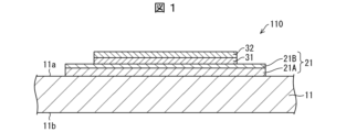
- FIG. 1 is a cross-sectional structural diagram showing a portion of a substrate according to a first embodiment of the present disclosure.
- 1 is a cross-sectional structural diagram showing a portion of an apparatus according to a first embodiment of the present disclosure.
- 1 is a micrograph of a cross section of an electrode and a joint according to a first embodiment of the present disclosure.
- 1 is a micrograph showing a further enlargement of the vicinity of the second layer of a cross section of an electrode and a joint according to a first embodiment of the present disclosure.
- FIG. 2 is a diagram showing a schematic diagram of the arrangement of ⁇ -Sn atoms in the [111] direction and the arrangement of Mo atoms in the [121] direction of a joint according to the first embodiment of the present disclosure.
- FIG. 1 is a cross-sectional structural diagram showing a portion of an electronic module including a device according to a first embodiment of the present disclosure.
- 11 is a cross-sectional view of an elastic wave device according to a second embodiment of the present disclosure.
- FIG. 1 is a micrograph of a joint of an electronic module of the present disclosure.
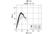
- 13 is a graph showing the results of evaluation of the bonding strength of the comparative example in Demonstration Test 2.
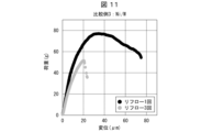
- 13 is a graph showing the results of evaluation of the bonding strength of the comparative example in Demonstration Test 2.
- 13 is a graph showing the results of evaluation of the bonding strength of the comparative example in Demonstration Test 2.
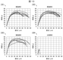
- 13 is a graph showing the results of evaluation of the bonding strength of the examples in Demonstration Test 2.
- FIG. 13 is a graph showing the results of evaluation of the bonding strength of the examples and the comparative examples in Demonstration Test 3.
- 13 is a graph showing the results of evaluation of the bonding strength of the examples in Demonstration Test 4.
- 13 is a graph showing the results of evaluation of the bonding strength of the examples in Demonstration Test 5.
- 13 is a graph showing the results of evaluation of the bonding strength of the examples in Demonstration Test 6.
- 13 is a graph showing the results of nanoindentation in Demonstration Test 8.
- 13 is a Weibull plot in Verification Test 9.
- FIG. 13 is a schematic diagram of an electrode structure prepared in an additional test.
- FIG. 1 is a diagram showing an outline of a steel ball drop test.
- 1 is a graph showing the results of a steel ball drop test. 13 shows the results of SEM observation after a drop test of a comparative example. 1 shows the results of SEM observation after a drop test in an embodiment. 1 shows the results of energy dispersive X-ray analysis (EDX) of the Mo electrode side of the fractured surface of the example electrode.
- EDX energy dispersive X-ray analysis
- sufficient interfacial strength can be ensured at the solder joint even after high-temperature processes such as reflow bonding.
- the device according to the present disclosure may be, for example, an electronic device including a substrate and electronic components such as electronic elements mounted on the substrate.
- An electronic module (electrical device) including the device is configured by mounting the device on a mounting substrate (module substrate).
- FIG. 1 is a cross-sectional view showing a portion of a substrate 110 according to embodiment 1 of the present disclosure.
- FIG. 1 is an enlarged cross-sectional view of a portion of the substrate 110 where an electrode 21 is located.
- the substrate 110 includes a base 11, an electrode 21, a barrier layer 31, and a bonding layer 32.
- the barrier layer 31 and the bonding layer 32 are layered in this order from the electrode 21 side.
- the substrate 110 is a substrate on which electronic components are mounted, and may include internal wiring located inside the substrate 110, and through conductors that connect the internal wirings vertically.
- the base 11 of the substrate 110 may be composed of a single layer or multiple layers.
- the base 11 has a first surface 11a and a second surface 11b located on the opposite side of the first surface 11a.
- An electronic component such as an electronic element may be mounted on either the first surface 11a or the second surface 11b.
- the base 11 has insulating properties.
- the material of the base 11 may be ceramics such as aluminum nitride sintered body, aluminum oxide sintered body (alumina ceramics), silicon nitride sintered body, mullite sintered body, or glass ceramic sintered body.
- the material of the base 11 may be resin such as epoxy resin, polyimide resin, acrylic resin, phenol resin, and fluorine resin. Examples of the fluorine resin include resins such as polyester resin and polytetrafluoroethylene resin.
- the base 11 may be a Si substrate.
- the base 11 may be formed by combining a support substrate made of Si with a piezoelectric substrate made of a single crystal material such as lithium tantalate (also called LiTaO 3 :LT) or lithium niobate (also called LiNbO 3 :LN).
- a support substrate made of Si with a piezoelectric substrate made of a single crystal material such as lithium tantalate (also called LiTaO 3 :LT) or lithium niobate (also called LiNbO 3 :LN).
- the electrode 21 of the substrate 110 electrically connects the device 200 including the substrate 110 to a circuit board.
- the electrode 21 is located on the first surface 11a of the base 11.
- the substrate 110 may include a plurality of electrodes 21 on the first surface 11a.
- the electrode 21 may include a wiring layer 21A that transmits signals and an adhesion layer 21B that improves adhesion between the wiring layer 21A and the barrier layer 31.
- the wiring layer 21A may include at least one of, for example, a Ni layer mainly composed of Ni (nickel), a Cu layer mainly composed of Cu (copper), a layer made of an alloy containing Ni (nickel) and Cu (copper), an Al layer mainly composed of Al (aluminum), and a Ti layer mainly composed of Ti (titanium).
- the adhesion layer 21B may include at least one of a layer mainly composed of Ti and a layer mainly composed of Cr. By including at least one of a layer mainly composed of Ti and a layer mainly composed of Cr in the adhesion layer 21B, the adhesion between the wiring layer 21A and the barrier layer 31 can be improved.
- the adhesion layer 21B may be composed only of a layer mainly composed of Ti.
- the adhesion layer 21B may be in contact with the barrier layer 31.
- the barrier layer 31 is referred to as the first layer 301 in the device 200 (see FIG. 2). Therefore, in the device 200, the adhesion layer 21B may be in contact with the first layer 301.
- the electrode structure has a laminated structure composed of a wiring layer, an adhesion layer, and a protective layer that protects the electrode and acts as a base for the barrier layer.
- the protective layer may be composed of, for example, a single Ni layer, or a multilayer of Ni and Au layers.
- the electrode 21 according to the present disclosure does not need to have a protective layer.
- the cost of the electrode 21 can be reduced and the electrode 21 can be made thinner.
- the substrate 110 may have a metallized layer on the surface of the base 11 in addition to the electrodes 21.
- the metallized layer includes, for example, a metallized layer that is provided in a mounting area on the base 11 where an electronic component is mounted and that can be electrically connected to the electronic component.
- the metallization layer may be made of, for example, any one of W (tungsten), Mo (molybdenum), Mn (manganese), Ag (silver), Ni, and Cu, or an alloy containing at least one of these.
- the metallization layer may be made of, for example, any one of Cu, Au (gold), Al (aluminum), Ni, Mo, and Ti, or an alloy containing at least one of these.
- the internal wiring and through conductors may also be of the same configuration as the metallization layer.
- the barrier layer 31 is a layer containing Mo as a main component.
- the manufacturing process of the device and electronic module including the substrate 110 includes a solder bonding process, which is a high-temperature process. For example, when a solder ball is placed and then heated, the molten high-temperature solder is applied onto the electrode 21. When reflow bonding is further performed, the device 200 or the electronic module 300 with the solder applied to the electrode portion is heated in a reflow furnace. In addition, the solder joint may be repeatedly or continuously exposed to a high temperature state due to heat generation of the module during use of the electronic module 300.
- the electrode metals such as Cu and Ni contained in the electrode 21 melt and react with metals such as Sn (tin) and Cu contained in the solder to form a metal compound.
- the metal compound is hard and brittle, and is likely to become the starting point of cracks.
- the thickness of the barrier layer 31 may be, for example, 0.1 ⁇ m or more. By making the barrier layer 31 have a thickness of 0.1 ⁇ m or more, it is possible to significantly reduce the possibility of the electrode metal reacting with the metal of the solder layer. This makes it possible to maintain the interface strength.
- the barrier layer 31 covers a portion of the electrode 21, but the barrier layer 31 may cover the entire exposed surface of the electrode 21.
- the bonding layer 32 is a layer located on the barrier layer 31 and containing at least one of Ni, Ag, Au, and Cu. The presence of the bonding layer 32 ensures the wettability of the solder, thereby improving the interfacial strength of the solder interface.
- the bonding layer 32 may be composed of a base layer located on the barrier layer 31 and a surface layer located on the base layer.
- the bonding layer 32 may have a laminated structure composed of a Ni layer positioned as a base layer on the barrier layer 31 and an Au layer positioned on the base layer. This configuration significantly improves wettability compared to, for example, a case in which a single Au layer is used as the bonding layer 32.
- the bonding layer 32 may include a layer made of a silver alloy mainly composed of Ag.
- the bonding layer 32 may have a laminated structure composed of a Ni layer located as a base layer on the barrier layer 31 and a layer made of a silver alloy located on the base layer.
- the silver alloy may be an alloy mainly composed of Ag, for example, APC available from Furuya Metal. This configuration can reduce costs compared to using an Au layer for the outermost layer of the bonding layer 32.
- a layer made of a silver alloy for the outermost layer of the bonding layer 32 wettability is further improved compared to using an Au layer.
- when the layer made of a silver alloy comes into contact with molten solder it dissolves slowly into the solder, so that dissolution of the electrode metal can be further reduced, especially when solder bonding is repeated.
- the thickness of the bonding layer 32 may be smaller than the thickness of the electrode 21.
- the thickness of the bonding layer 32 may be 0.1 ⁇ m or more and 1 ⁇ m or less, or may be 0.1 ⁇ m.
- the metal contained in the bonding layer 32 may react with the metal contained in the solder to form a metal compound.
- the bonding layer 32 By making the bonding layer 32 have the thickness described above, the amount of metal eluted from the bonding layer 32 during solder bonding, etc., can be reduced, and the amount of metal compounds formed can be reduced.
- the amount of metal eluted from a sufficiently thin bonding layer 32 is small, coarse particles of metal compounds are less likely to form and the layer is less likely to become brittle.
- a bonding portion 30 having excellent interfacial strength can be achieved while ensuring the wettability of the solder. The bonding portion 30 will be described later.
- Fig. 2 is a cross-sectional structural view showing a part of the device 200 according to the first embodiment of the present disclosure.
- Fig. 2 is an enlarged cross-sectional structural view of an electrode 21 portion of the device 200, and electronic components and the like included in the device 200 are not shown.
- the device 200 according to the present disclosure is obtained, for example, by placing solder balls on the substrate 110 shown in FIG. 1 and then heating it. More specifically, the method of manufacturing the device 200 includes (1) a step of preparing the substrate 110, and (2) a step of placing solder on the bonding layer 32 of the substrate 110 and heating it to create a bonding portion 30 on the electrode 21.
- the step (1) will be referred to below as the substrate preparation step, and the step (2) as the bonding portion creation step.
- the device 200 has a substrate 11, an electrode 21, and a joint 30.
- the joint 30 is located on the electrode 21, and includes, from the electrode 21 side, a first layer 301, a second layer 302, and a third layer 303.
- Figure 3 is a scanning transmission electron microscopy (STEM) photograph of a cross section of the electrode 21 and the joint 30.
- Figure 4 is a STEM photograph of a further enlargement of the vicinity of the second layer 302 of the cross section of the electrode 21 and the joint 30.
- the cross-sectional photographs of Figures 3 and 4 were obtained by cutting out a portion of the device 200 including the electrode 21 and the joint 30 using a focused ion beam (FIB) method and photographing it using a STEM.
- FIB focused ion beam
- the first layer 301 is a layer containing Mo as a main component.
- the first layer 301 in the device 200 corresponds to the barrier layer 31 of the substrate 110.
- the barrier layer 31 remains almost unchanged even after repeated heating and reflow bonding after the solder balls are placed on it, and is located in the joint 30 as the first layer 301.
- the second layer 302 is a layer containing ⁇ -Sn as a main component.
- the second layer 302 is formed when the substrate 110 according to the present disclosure is solder-joined.
- the second layer 302 in the device 200 is formed in the above-mentioned joint fabrication process.
- the metal compound may be a Sn compound.
- the joining layer 32 before solder joining is mainly composed of Ni
- at least one compound of Ni 3 Sn 4 , Ni 3 Sn 2 , Ni 3 Sn, (Cu, Ni) 3 Sn 4 , and (Cu, Ni) 6 Sn 5 may be formed.
- the metal compound may be formed as a compound mass in the third layer 303 near the second layer 302 (see FIG. 3).
- the third layer 303 may contain a metal compound formed by the reaction of the metal contained in the joining layer 32 and the metal contained in the solder.
- the bonding layer 32 is incorporated into the third layer 303, forming a metal compound, while the second layer 302 is formed between the third layer 303 and the first layer 301.
- the second layer 302 is formed by the growth of oriented ⁇ -Sn crystals near the first layer 301 when the solder that becomes the third layer 303 melts.
- the growth of the ⁇ -Sn crystals is due to the fact that the first layer 301 is a layer mainly composed of Mo.
- the inventors have confirmed that when tungsten is used as the barrier layer, a layer mainly composed of ⁇ -Sn is not formed.
- the second layer 302 may be located over the entire surface between the first layer 301 and the third layer 303. Alternatively, there may be a region between the first layer 301 and the third layer 303 where the second layer 302 is not present. Also, a portion of the bonding layer 32 of the substrate 110 may remain between the first layer 301 and the third layer 303.
- FIG. 30 is a schematic diagram showing the arrangement of atoms in the [111] direction of ⁇ -Sn and the arrangement of atoms in the [121] direction of Mo.
- the interatomic distance d( ⁇ -Sn) in the ⁇ 112 ⁇ plane of ⁇ -Sn is 1.4843 ⁇
- the interatomic distance d(Mo) in the ⁇ 110 ⁇ plane of Mo is 2.2254 ⁇ .
- the ⁇ 111 ⁇ plane of Mo and the ⁇ 110 ⁇ plane of ⁇ -Sn are approximately parallel to each other, resulting in a characteristic match in the interatomic distances between the two layers as described above, which allows the strength of the interface between the first layer 301 and the second layer 302 to be maintained.
- the device 200 according to the present disclosure can significantly improve impact resistance. This can improve the joint reliability of the electronic module.
- a metal layer (e.g., Au, etc.) provided on the electrode to improve the wettability of the solder may form a metal compound when heated, which may cause the molten solder to be repelled at the interface between the electrode and the solder during reflow bonding.
- the device 200 according to the present disclosure can maintain the wettability and spreading of the solder even during reflow bonding.
- the electronic module 300 includes the base 11 and electrode 21 of the device 200, the base 12 and electrode 22 of the mounting board 120, and a joint 30.
- the electronic module 300 has a configuration in which the electrode 21 of the device 200 and the electrode 22 of the mounting board 120 are joined by the joint 30.
- the joint 30 includes, in order from the side of each of the electrodes 21 and 22, a first layer 301, a second layer 302, and a third layer 303.
- the first layer 301, the second layer 302, and the third layer 303 are configured as described above.
- the elastic wave device 210 has a base 13, an electrode layer 23, and a joint 30.
- the elastic wave device 210 can be mounted on a circuit board (mounting board) of a communication device.
- the electrode layer 23 includes an IDT (Interdigital Transducer) electrode 231 and a pad portion 232.
- the pad portion 232 includes a first pad 232A and a second pad 232B.
- the pad portion 232 in this embodiment is an example of the electrode 21 according to the present disclosure.
- the first pad 232A and the second pad 232B are laminated in this order from the base 13 side. In other words, the pad portion 232 may include multiple layers.
- the first pad 232A may have the same thickness as the IDT electrode 231.
- the pad portion 232 has a laminated structure, which can reduce electrical resistance.
- the elastic wave device 210 is obtained by joining solder to the substrate 130.
- the substrate 130 has a barrier layer and a bonding layer according to the present disclosure on the pad portion 232.
- the substrate 130 is an example of a substrate according to the present disclosure.
- the bonding portion 30 is located on the pad portion 232, and includes, in order from the pad portion 232 side, a first layer 301, a second layer 302, and a third layer 303.
- the first layer 301, the second layer 302, and the third layer 303 are layered in this order from the pad portion 232 side.
- the first layer 301, the second layer 302, and the third layer 303 are configured as described in the first embodiment.
- the IDT electrode 231 is a comb-shaped electrode that generates an elastic wave in the elastic wave device.
- the IDT electrode 231 is composed of a pair of electrodes to which an AC voltage is applied.
- the IDT electrode 231 is electrically connected to the pad portion 232.
- the elastic wave device 210 has fewer joints that are bonded via the joints 30. Therefore, ensuring the interfacial strength at the joints 30 is more important. Since the elastic wave device 210 has the substrate 130 and the joints 30, sufficient interfacial strength can be ensured at the solder joints even after high-temperature processes such as reflow bonding. Furthermore, by having the second layer 302, the solder can maintain its wetting and spreading even after high-temperature processes such as reflow bonding. This makes it possible to realize an elastic wave device with excellent bonding reliability. Furthermore, due to the properties of the second layer 302, an elastic wave device with excellent impact resistance can be realized.
- a SAW Surface Acoustic Wave
- BAW Bulk Acoustic Wave
- FIG. 8 is a micrograph of the joint 30 of the electronic module.
- Reference numeral 8001 in FIG. 8 is a micrograph of the joint 30 in the electronic module 300 according to the embodiment of the present disclosure.
- Reference numeral 8002 in FIG. 8 is a micrograph of the joint of the electronic module as a comparative example.
- a solder layer is located between the electrode on the electronic device side and the mounting board. In other words, it does not have the first layer 301 and the second layer 302 according to the present disclosure.
- the electronic module of the comparative example is an electronic device and a mounting board that do not have the barrier layer 31 and the bonding layer 32 according to the present disclosure on the electrodes and are bonded by solder.
- the heating conditions during solder bonding are the same for both the embodiment and the comparative example.
- a region C containing a large amount of a compound formed by a reaction between the electrode metal and the metal contained in the solder layer exists as a coarse granular region near the interface of the joint.
- a large amount of the electrode metal has dissolved toward the solder layer, forming a void P at the interface of the joint.
- the area C near the interface of the joint 30 remains a relatively small area.
- the void P observed in the comparative example was not observed.
- a device manufactured using a substrate having the barrier layer 31 and bonding layer 32 according to the present disclosure has a bonding portion including a first layer 301 and a second layer 302. It has been demonstrated that a device having a bonding portion including the first layer 301 and the second layer 302 can significantly reduce the formation of brittle compounds at the solder bonding portion even after undergoing high-temperature processes such as reflow bonding. It has also been demonstrated that the barrier layer 31 reduces the elution of the electrode metal onto the solder layer side, thereby reducing the possibility of voids occurring at the interface between the electrode and the bonding portion.
- the graphs show no sudden drop in load within the test range of displacement, whether the reflow process was performed once or three times. In other words, it was demonstrated that the interfacial strength was maintained within the test range of displacement.
- (Demonstration Test 4: Bonding Strength Test 3 - Verification of Bonding Strength with and without Protective Layer) 14 is a graph showing the results of evaluating the bonding strength of electrodes according to the present disclosure when the electrodes have a protective layer and when they do not have a protective layer.
- the evaluation test of the bonding strength was performed in accordance with the solder ball shear standard of JEDEC JESD22-B117.
- Example 2 has a layered structure in which the electrode is composed of an Al layer as a wiring layer, a Ti layer as an adhesion layer, and a Ni layer as a protective layer.
- Example 5 indicates the results of Example 5, in which the electrode has a laminated structure consisting of an Al layer as a wiring layer and a Ti layer as an adhesion layer. In other words, Example 5 does not have a Ni layer as a protective layer, and has a configuration in which the adhesion layer is in contact with the barrier layer. Example 5 has a configuration within the scope of this disclosure.
- Example 5 the load did not suddenly drop within the displacement test range, demonstrating that the interfacial strength was maintained within the displacement test range.
- the sample used for observing the cross-sectional structure in Demonstration Test 5 was prepared by placing a solder ball on the following substrate sample, and then reflow-joining it to the following mother substrate sample.
- Substrate sample Base—Si substrate, electrode—layered structure of Ni layer (0.6 ⁇ m) and Ti layer (0.05 ⁇ m), barrier layer—Mo layer (0.3 ⁇ m), bonding layer—layered structure of Ni layer (0.2 ⁇ m) and Au layer (0.05 ⁇ m).
- Mother substrate sample Base—Si substrate, electrode—layered structure of Ni layer (0.6 ⁇ m) and Ti layer (0.05 ⁇ m), barrier layer—Mo layer (0.3 ⁇ m), bonding layer—layered structure of Ni layer (0.2 ⁇ m) and Au layer (0.05 ⁇ m).
- the electronic module disclosed herein has been demonstrated to have sufficient bonding reliability in a temperature cycle test of 300 cycles from -40°C to 85°C.
- Example 7 The example sample (Example 7) and the comparative example sample (Comparative Example 6) used in Demonstration Test 8 were prepared as follows.
- Example 8 Substrate sample: Base—Si substrate, electrode—layered structure of Ti layer (0.015 ⁇ m) and Ni layer (0.3 ⁇ m), barrier layer—Mo layer (0.3 ⁇ m), bonding layer—layered structure of Ni layer (0.1 ⁇ m) and Au layer (0.05 ⁇ m).
- Mother substrate sample Base—Si substrate, electrode—layered structure of Ti layer (0.015 ⁇ m) and Ni layer (0.3 ⁇ m), barrier layer—Mo layer (0.3 ⁇ m), bonding layer—layered structure of Ni layer (0.1 ⁇ m) and Au layer (0.05 ⁇ m).
- Comparative Example 9 Substrate sample: base—Si substrate, electrode—Ti layer (0.050 ⁇ m), bonding layer—Ni layer (0.6 ⁇ m) and APC layer (0.1 ⁇ m) laminated structure.
- Mother substrate sample base—Si substrate, electrode—Ti layer (0.050 ⁇ m), bonding layer—Ni layer (0.6 ⁇ m) and APC layer (0.1 ⁇ m) laminated structure.
- FIG. 19 A schematic diagram of the electrode structure produced is shown in FIG. 19.
- Reference numeral 1901 in FIG. 19 indicates a general-purpose Ni/Au electrode as a comparative example.
- the Ni thickness was set to 1.2 ⁇ m to avoid Ni loss due to dissolution.
- FIG. 19 indicates a Ni/Mo/Ni/Au electrode as an example of the present disclosure, in which a Mo barrier layer was formed on Ni having a thickness of 0.6 ⁇ m.
- the Mo barrier layer is an example of a barrier layer according to the present disclosure.
- Reference numeral 1903 in FIG. 19 indicates an electrode in which Mo/Ni/Au is formed directly on a Ti seed layer as an example of the present disclosure.
- the Mo layer shown in the example of reference numeral 1903 is also an example of a barrier layer according to the present disclosure.
- FIG 22 shows the results of SEM observations of a comparative Ni/Au electrode after a drop test (five drops).
- Ni has dissolved and disappeared over a width of about 5 ⁇ m from the outer periphery of the electrode, which is considered to be the starting point of the destruction. It is presumed that a crack generated from this Ni disappearance part as an initial defect propagates through the Si interface and leads to the destruction of the Si chip.
- the dissolution and disappearance of the Ni electrode occurs because the thickness of the outer periphery is thin after film formation, but it is difficult to avoid in the process because it is caused by being shadowed by the resist during sputtering.
- FIG. 23 shows the results of SEM observation of the Ni/Mo/Ni/Au electrode of the embodiment of the present disclosure after a drop test (drop count 289 times). Striations shown by reference numeral 2302 in FIG. 23 were observed from the outer periphery of the fractured surface of the solder bump shown by reference numeral 2301 in FIG. 23 to the region of the dashed line. The striation interval was about 50 nm, and the distance from the outer periphery to the dashed line was a maximum of 20 ⁇ m. From this, it is not inconsistent to think that the fatigue cracks propagated to the dashed line due to the repeated dropping of the steel ball, leading to macroscopic destruction. Reference numeral 2303 in FIG.
- Figure 24 shows the results of energy dispersive X-ray analysis (EDX) of the Mo layer side of the fracture surface of a Ni/Mo/Ni/Au electrode, which is an example of this disclosure.
- EDX energy dispersive X-ray analysis
- the fracture morphology of the Mo/Ni/Au electrode which is an example of the present disclosure, was similar to that of the Ni/Mo/Ni/Au electrode. By removing the Ni layer, it is expected that the electrode can be made even thinner and the deposition time can be shortened, thereby improving productivity.
- the thin outer periphery of the electrode becomes an initial defect and leads to chip destruction, but the Mo barrier layer prevents dissolution, improving impact resistance.
- destruction of the electrode structure including the Mo barrier layer is mainly a ductile fracture that occurs at the ⁇ -Sn/solder interface.
- a device has a base having a first surface, an electrode located on the first surface of the base, and a joint located on the electrode, the joint including, in order from the electrode side, a first layer, a second layer, and a third layer, the first layer including Mo as a main component, the second layer including ⁇ -Sn as a main component, and the third layer including solder.
- the electrode in the above-mentioned aspect 1, includes a wiring layer that transmits signals and an adhesion layer that improves adhesion between the wiring layer and the first layer, and the adhesion layer is in contact with the first layer.
- the device according to the third aspect of the present disclosure is the device according to the second aspect above, in which the adhesion layer includes at least one of a layer mainly composed of Ti and a layer mainly composed of Cr.
- the device according to the fifth aspect of the present disclosure is any one of the aspects 1 to 4 above, in which the ⁇ 111 ⁇ plane of Mo contained in the first layer and the ⁇ 110 ⁇ plane of ⁇ -Sn contained in the second layer are approximately parallel.
- An electrical device includes any one of the devices according to aspects 1 to 6 above.
- a substrate according to an eighth aspect of the present disclosure has a base having a first surface, an electrode located on the first surface of the base, a barrier layer located on the electrode, and a bonding layer located on the barrier layer, the barrier layer containing Mo as a main component, and the bonding layer containing at least one of Ni, Ag, Au, and Cu.
- the ninth aspect of the present disclosure relates to a substrate according to the eighth aspect, in which the bonding layer includes a layer made of a silver alloy containing Ag as a main component.
- a method of manufacturing a device includes the steps of preparing a substrate according to aspect 8 or 9 above, and placing solder on the bonding layer and heating it to create a bonding portion on the electrode, the bonding portion including, from the electrode side, a first layer, a second layer, and a third layer, the first layer including Mo as a main component, the second layer including ⁇ -Sn as a main component, and the third layer including solder.
Landscapes
- Physics & Mathematics (AREA)
- Acoustics & Sound (AREA)
- Electric Connection Of Electric Components To Printed Circuits (AREA)
Priority Applications (2)
| Application Number | Priority Date | Filing Date | Title |
|---|---|---|---|
| CN202480033661.6A CN121195334A (zh) | 2023-05-25 | 2024-01-22 | 装置、电气装置、基板和装置的制造方法 |
| JP2025521798A JPWO2024241628A1 (https=) | 2023-05-25 | 2024-01-22 |
Applications Claiming Priority (2)
| Application Number | Priority Date | Filing Date | Title |
|---|---|---|---|
| JP2023-086298 | 2023-05-25 | ||
| JP2023086298 | 2023-05-25 |
Publications (1)
| Publication Number | Publication Date |
|---|---|
| WO2024241628A1 true WO2024241628A1 (ja) | 2024-11-28 |
Family
ID=93589924
Family Applications (1)
| Application Number | Title | Priority Date | Filing Date |
|---|---|---|---|
| PCT/JP2024/001574 Ceased WO2024241628A1 (ja) | 2023-05-25 | 2024-01-22 | 装置、電気装置、基板および装置の製造方法 |
Country Status (3)
| Country | Link |
|---|---|
| JP (1) | JPWO2024241628A1 (https=) |
| CN (1) | CN121195334A (https=) |
| WO (1) | WO2024241628A1 (https=) |
Citations (5)
| Publication number | Priority date | Publication date | Assignee | Title |
|---|---|---|---|---|
| JPH04180230A (ja) * | 1990-11-15 | 1992-06-26 | Fujitsu Ltd | 半導体装置 |
| JP2000332343A (ja) * | 1999-05-21 | 2000-11-30 | Sharp Corp | 半導体発光装置およびその製造方法 |
| JP2006108604A (ja) * | 2004-09-08 | 2006-04-20 | Denso Corp | 半導体装置およびその製造方法 |
| JP2007115941A (ja) * | 2005-10-21 | 2007-05-10 | Kyocera Corp | 窒化ガリウム系化合物半導体及び発光素子 |
| WO2015022931A1 (ja) * | 2013-08-14 | 2015-02-19 | 株式会社村田製作所 | 弾性波装置、電子部品、および弾性波装置の製造方法 |
-
2024
- 2024-01-22 CN CN202480033661.6A patent/CN121195334A/zh active Pending
- 2024-01-22 WO PCT/JP2024/001574 patent/WO2024241628A1/ja not_active Ceased
- 2024-01-22 JP JP2025521798A patent/JPWO2024241628A1/ja active Pending
Patent Citations (5)
| Publication number | Priority date | Publication date | Assignee | Title |
|---|---|---|---|---|
| JPH04180230A (ja) * | 1990-11-15 | 1992-06-26 | Fujitsu Ltd | 半導体装置 |
| JP2000332343A (ja) * | 1999-05-21 | 2000-11-30 | Sharp Corp | 半導体発光装置およびその製造方法 |
| JP2006108604A (ja) * | 2004-09-08 | 2006-04-20 | Denso Corp | 半導体装置およびその製造方法 |
| JP2007115941A (ja) * | 2005-10-21 | 2007-05-10 | Kyocera Corp | 窒化ガリウム系化合物半導体及び発光素子 |
| WO2015022931A1 (ja) * | 2013-08-14 | 2015-02-19 | 株式会社村田製作所 | 弾性波装置、電子部品、および弾性波装置の製造方法 |
Also Published As
| Publication number | Publication date |
|---|---|
| JPWO2024241628A1 (https=) | 2024-11-28 |
| CN121195334A (zh) | 2025-12-23 |
Similar Documents
| Publication | Publication Date | Title |
|---|---|---|
| KR100531393B1 (ko) | 반도체 장치 및 그 제조 방법 | |
| US5821627A (en) | Electronic circuit device | |
| JP5773344B2 (ja) | 半導体装置及び半導体装置用接合材 | |
| JP2004006872A (ja) | 半田で取着された装置の疲労抵抗性を向上させるための歪み吸収金属層 | |
| CN85108637A (zh) | 电子电路器件及其制造方法 | |
| CN102017107B (zh) | 接合结构以及电子器件 | |
| JP2009076703A (ja) | 半導体装置 | |
| CN100546180C (zh) | 表面声波装置及其制造方法 | |
| TW201231206A (en) | Solder, soldering method, and semiconductor device | |
| JP6439472B2 (ja) | 電子装置及び電子装置の製造方法 | |
| JP3356649B2 (ja) | 半導体装置及びその製造方法 | |
| JP3262657B2 (ja) | ボンディング方法及びボンディング構造 | |
| US6742248B2 (en) | Method of forming a soldered electrical connection | |
| WO2024241628A1 (ja) | 装置、電気装置、基板および装置の製造方法 | |
| JP2001060760A (ja) | 回路電極およびその形成方法 | |
| JP2001127375A (ja) | 光半導体素子搭載用サブマウント | |
| JP2697116B2 (ja) | インジウム半田の接合構造 | |
| JP3284055B2 (ja) | 半導体素子、半導体装置、および半導体装置の検査方法 | |
| JP3407839B2 (ja) | 半導体装置のはんだバンプ形成方法 | |
| JPH08293522A (ja) | 半導体装置の耐熱電極 | |
| JP2002160089A (ja) | 気密端子およびその製造方法 | |
| JP4910789B2 (ja) | パワー素子搭載用基板およびパワー素子搭載用基板の製造方法並びにパワーモジュール | |
| WO2024090143A1 (ja) | 装置、電気装置および基板 | |
| JP3373701B2 (ja) | 半導体素子、半導体装置およびその製造方法 | |
| JP5387388B2 (ja) | 電極構造 |
Legal Events
| Date | Code | Title | Description |
|---|---|---|---|
| 121 | Ep: the epo has been informed by wipo that ep was designated in this application |
Ref document number: 24810637 Country of ref document: EP Kind code of ref document: A1 |
|
| ENP | Entry into the national phase |
Ref document number: 2025521798 Country of ref document: JP Kind code of ref document: A |
|
| NENP | Non-entry into the national phase |
Ref country code: DE |