WO2024232271A1 - プローブ装置、プローブ装置の制御方法、検査システム及び検査システムの制御方法 - Google Patents
プローブ装置、プローブ装置の制御方法、検査システム及び検査システムの制御方法 Download PDFInfo
- Publication number
- WO2024232271A1 WO2024232271A1 PCT/JP2024/016069 JP2024016069W WO2024232271A1 WO 2024232271 A1 WO2024232271 A1 WO 2024232271A1 JP 2024016069 W JP2024016069 W JP 2024016069W WO 2024232271 A1 WO2024232271 A1 WO 2024232271A1
- Authority
- WO
- WIPO (PCT)
- Prior art keywords
- control unit
- unit
- inspection system
- measurement
- probe
- Prior art date
- Legal status (The legal status is an assumption and is not a legal conclusion. Google has not performed a legal analysis and makes no representation as to the accuracy of the status listed.)
- Ceased
Links
Images




Classifications
-
- G—PHYSICS
- G01—MEASURING; TESTING
- G01R—MEASURING ELECTRIC VARIABLES; MEASURING MAGNETIC VARIABLES
- G01R31/00—Arrangements for testing electric properties; Arrangements for locating electric faults; Arrangements for electrical testing characterised by what is being tested not provided for elsewhere
- G01R31/28—Testing of electronic circuits, e.g. by signal tracer
- G01R31/2851—Testing of integrated circuits [IC]
- G01R31/2886—Features relating to contacting the IC under test, e.g. probe heads; chucks
- G01R31/2887—Features relating to contacting the IC under test, e.g. probe heads; chucks involving moving the probe head or the IC under test; docking stations
-
- G—PHYSICS
- G01—MEASURING; TESTING
- G01R—MEASURING ELECTRIC VARIABLES; MEASURING MAGNETIC VARIABLES
- G01R1/00—Details of instruments or arrangements of the types included in groups G01R5/00 - G01R13/00 and G01R31/00
- G01R1/02—General constructional details
- G01R1/06—Measuring leads; Measuring probes
- G01R1/067—Measuring probes
-
- G—PHYSICS
- G01—MEASURING; TESTING
- G01R—MEASURING ELECTRIC VARIABLES; MEASURING MAGNETIC VARIABLES
- G01R1/00—Details of instruments or arrangements of the types included in groups G01R5/00 - G01R13/00 and G01R31/00
- G01R1/02—General constructional details
- G01R1/06—Measuring leads; Measuring probes
- G01R1/067—Measuring probes
- G01R1/073—Multiple probes
- G01R1/07307—Multiple probes with individual probe elements, e.g. needles, cantilever beams or bump contacts, fixed in relation to each other, e.g. bed of nails fixture or probe card
- G01R1/07342—Multiple probes with individual probe elements, e.g. needles, cantilever beams or bump contacts, fixed in relation to each other, e.g. bed of nails fixture or probe card the body of the probe being at an angle other than perpendicular to test object, e.g. probe card
-
- G—PHYSICS
- G01—MEASURING; TESTING
- G01R—MEASURING ELECTRIC VARIABLES; MEASURING MAGNETIC VARIABLES
- G01R31/00—Arrangements for testing electric properties; Arrangements for locating electric faults; Arrangements for electrical testing characterised by what is being tested not provided for elsewhere
- G01R31/26—Testing of individual semiconductor devices
-
- G—PHYSICS
- G01—MEASURING; TESTING
- G01R—MEASURING ELECTRIC VARIABLES; MEASURING MAGNETIC VARIABLES
- G01R31/00—Arrangements for testing electric properties; Arrangements for locating electric faults; Arrangements for electrical testing characterised by what is being tested not provided for elsewhere
- G01R31/28—Testing of electronic circuits, e.g. by signal tracer
-
- G—PHYSICS
- G01—MEASURING; TESTING
- G01R—MEASURING ELECTRIC VARIABLES; MEASURING MAGNETIC VARIABLES
- G01R31/00—Arrangements for testing electric properties; Arrangements for locating electric faults; Arrangements for electrical testing characterised by what is being tested not provided for elsewhere
- G01R31/28—Testing of electronic circuits, e.g. by signal tracer
- G01R31/2851—Testing of integrated circuits [IC]
- G01R31/2886—Features relating to contacting the IC under test, e.g. probe heads; chucks
- G01R31/2891—Features relating to contacting the IC under test, e.g. probe heads; chucks related to sensing or controlling of force, position, temperature
-
- H—ELECTRICITY
- H10—SEMICONDUCTOR DEVICES; ELECTRIC SOLID-STATE DEVICES NOT OTHERWISE PROVIDED FOR
- H10P—GENERIC PROCESSES OR APPARATUS FOR THE MANUFACTURE OR TREATMENT OF DEVICES COVERED BY CLASS H10
- H10P74/00—Testing or measuring during manufacture or treatment of wafers, substrates or devices
-
- H—ELECTRICITY
- H10—SEMICONDUCTOR DEVICES; ELECTRIC SOLID-STATE DEVICES NOT OTHERWISE PROVIDED FOR
- H10P—GENERIC PROCESSES OR APPARATUS FOR THE MANUFACTURE OR TREATMENT OF DEVICES COVERED BY CLASS H10
- H10P74/00—Testing or measuring during manufacture or treatment of wafers, substrates or devices
- H10P74/23—Testing or measuring during manufacture or treatment of wafers, substrates or devices characterised by multiple measurements, corrections, marking or sorting processes
-
- H—ELECTRICITY
- H10—SEMICONDUCTOR DEVICES; ELECTRIC SOLID-STATE DEVICES NOT OTHERWISE PROVIDED FOR
- H10P—GENERIC PROCESSES OR APPARATUS FOR THE MANUFACTURE OR TREATMENT OF DEVICES COVERED BY CLASS H10
- H10P74/00—Testing or measuring during manufacture or treatment of wafers, substrates or devices
- H10P74/27—Structural arrangements therefor
Definitions
- This disclosure relates to a probe device, a control method for a probe device, an inspection system, and a control method for an inspection system.
- a semiconductor inspection system that inspects semiconductors includes, for example, an inspection device (tester) that performs electrical inspection of the object to be measured, and a probe device (prober) that moves the object to a position where the tester inspects it (for example, Patent Document 1 and Patent Document 2).
- This disclosure provides technology that adds multi-functionality to a probe device.
- a probe device that includes a support section that supports an object to be inspected, a drive section that moves the support section and adjusts the attitude of the support section, and a control section, in which the control section executes (a) a process of controlling the drive section so as to position the object to be inspected at a predetermined position, and (b) a process of inspecting the object to be inspected based on the measurement results of the characteristics of the object to be inspected.
- This disclosure provides technology that adds multi-functionality to a probe device.
- FIG. 1 is a diagram showing an outline of an inspection system according to the present embodiment.
- FIG. 2 is a diagram showing the overall configuration of an inspection system according to this embodiment.
- FIG. 3 is a diagram for explaining the hardware configuration of a control unit in a probe device provided in the inspection system according to this embodiment.
- FIG. 4 is a diagram for explaining the hardware configuration of a measurement control unit in a measurement device provided in the inspection system according to this embodiment.
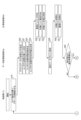
- FIG. 5 is a flow diagram (part 1) for explaining the processing of the inspection system according to this embodiment.
- FIG. 6 is a flow diagram (part 2) for explaining the processing of the inspection system according to this embodiment.
- FIG. 7 is a flow diagram (part 3) for explaining the processing of the inspection system according to this embodiment.
- FIG. 1 is a diagram showing an outline of an inspection system according to the present embodiment.
- FIG. 2 is a diagram showing the overall configuration of an inspection system according to this embodiment.
- FIG. 3 is a diagram for explaining the hardware configuration of a control unit in
- FIG. 8 is a diagram illustrating the availability of the calculation unit when the inspection system according to this embodiment is operated.
- FIG. 9 is a diagram for explaining the availability of the calculation unit when the inspection system of the reference example is operated.
- FIG. 10 is a diagram showing an outline of an inspection system according to a reference example.
- FIG. 11 is a flow diagram (part 1) for explaining the process of the inspection system of the reference example.
- FIG. 12 is a flow diagram (part 2) illustrating the process of the inspection system of the reference example.
- FIG. 13 is a flow diagram (part 3) for explaining the process of the inspection system of the reference example.
- the inspection system according to this embodiment includes a probe device and a measuring device that measures the characteristics of the inspection object.
- the probe device in the inspection system according to this embodiment includes a support section that supports the inspection object, a drive section that moves the support section and adjusts the attitude of the support section, and a control section.
- the control section in the inspection system according to this embodiment (a) executes a process of controlling the drive section so as to position the inspection object at a predetermined position.
- the control section in the inspection system according to this embodiment (b) executes a process of inspecting the inspection object based on the measurement results from the measuring device that measures the characteristics of the inspection object.
- FIG. 1 is a diagram showing an overview of an inspection system 1, which is an example of an inspection system according to this embodiment.
- FIG. 2 is a diagram showing the overall configuration of an inspection system 1, which is an example of an inspection system according to this embodiment.
- the inspection system 1 inspects, for example, a device formed on a semiconductor substrate.
- the inspection system 1 includes a probe device 10 and a measurement device 20.
- the probe apparatus 10 transports the DUT (Device Under Test) to be tested so that it can be measured by the measuring apparatus 20.
- the probe apparatus 10 moves the DUT to a predetermined position, for example, a position where the measuring apparatus 20 can measure it.
- the probe apparatus 10 then adjusts the DUT to a predetermined posture, for example, a posture where the probe 14A can come into contact so that the measuring apparatus 20 can measure it.
- the probe apparatus 10 aligns the DUT to be tested so that the measuring apparatus 20 can measure it.
- the probe device 10 also controls the overall testing in the testing system 1.
- the probe device 10 controls the measuring device 20 to perform a predetermined test.
- the probe device 10 then performs testing of the DUT to be tested based on the results of measurements made by the measuring device 20.
- the measuring device 20 measures the electrical characteristics of the DUT under test.
- the probe apparatus 10 transports a DUT to be tested.
- the probe apparatus 10 also aligns the DUT to be tested with the probes 14A of the probe card 14 so that the measuring device 20 can perform measurement.
- the probe device 10 includes a loader chamber 11 and a prober chamber 12.
- the probe device 10 transports a wafer W, which is a DUT to be inspected, from the loader chamber 11.
- the prober chamber 12 is adjacent to the loader chamber 11. In the prober chamber 12, the electrical characteristics of the wafer W transported from the loader chamber 11 are inspected.
- the probe device 10 is equipped with a display unit 18.
- the display unit 18 displays the results of the test, etc.
- the probe device 10 includes a prober chamber 12, a support section 13, a probe card 14, an insert ring 15, an alignment mechanism 16, and a drive section 19.
- the support unit 13 supports the wafer W, which is the DUT to be tested.
- the drive unit 19 moves the support unit 13 in three mutually orthogonal axial directions, the X-axis, the Y-axis, and the Z-axis, and rotates it around each of the X-axis, the Y-axis, and the Z-axis.
- the X-axis and Y-axis directions are horizontal directions, and the Z-axis direction is vertical.
- the probe device 10 aligns the wafer W, which is the DUT to be tested, with the multiple probes 14A on the probe card 14.
- the drive unit 19 moves the wafer W, which is the DUT to be tested, to a predetermined position and adjusts it so that it is in a predetermined posture.
- the probe card 14 has multiple probes 14A that contact electrodes formed on the wafer W, which is the DUT to be tested.
- the probe card 14 is also electrically connected to the test head 21 via the insert ring 15.
- the probe card 14 is placed above the support portion 13.
- the alignment mechanism 16 aligns the probes 14A on the probe card 14 with the electrode pads on the wafer W, which is the DUT to be tested and is supported on the support 13.
- the alignment mechanism 16 includes an alignment bridge 16A, a CCD camera 16B, and a CCD camera 16C.
- the alignment bridge 16A moves horizontally between the rear surface of the prober chamber 12 and the probe center.
- the CCD camera 16B is provided on the alignment bridge 16A.
- the CCD camera 16C is provided on the side of the support portion 13.
- the alignment mechanism 16 aligns the probe card 14 with the wafer W supported on the support 13.
- the CCD camera 16B advances from the rear of the prober chamber to the probe center via the alignment bridge 16A.
- the CCD camera 16B is positioned between the probe card 14 and the support 13.
- the CCD camera 16B detects the electrode pads on the wafer W from above while the support 13 moves in the X-axis and Y-axis directions.
- the CCD camera 16C sequentially detects the specified probes 14A from below the probe card 14 while the support part 13 moves in the X-axis and Y-axis directions below the probe card 14.
- the control unit 17 controls various components including the drive unit 19 and the alignment mechanism 16.
- the control unit 17 is, for example, a computer.
- the control unit 17 controls the drive unit 19 and the alignment mechanism 16 so as to align the wafer W supported by the support unit 13 with the multiple probes 14A in the probe card 14.
- the control unit 17 then controls the drive unit 19 and the alignment mechanism 16 so as to electrically contact the multiple probes 14A with electrodes formed on the wafer W.
- the control unit 17 may, for example, adjust the temperature in the prober chamber 12 so that the inspection system 1 performs high-temperature inspection or low-temperature inspection of the wafer W.
- FIG. 3 is a diagram illustrating the hardware configuration of the control unit 17 in the probe device 10 provided in the inspection system 1, which is an example of an inspection system according to this embodiment.
- the control unit 17 includes a calculation unit 17A, a main memory unit 17B, an external memory unit 17C, a clock unit 17D, an input unit 17E, a transmission/reception unit 17F, and an output unit 17G.
- a calculation unit 17A a main memory unit 17B, an external memory unit 17C, a clock unit 17D, an input unit 17E, a transmission/reception unit 17F, and an output unit 17G.
- Each of the calculation unit 17A, the main memory unit 17B, the external memory unit 17C, the clock unit 17D, the input unit 17E, the transmission/reception unit 17F, and the output unit 17G is connected to a bus 17H.
- the display unit 18 is connected to the control unit 17.
- the display unit 18 displays, for example, various data such as the target temperature during the inspection input from the input unit 17E, image data such as the images captured by the CCD cameras 16B and 16C, and the like.
- the calculation unit 17A is mainly composed of a processor such as a CPU (Central Processing Unit).
- the main memory unit 17B is composed of a volatile memory such as a RAM (Random Access Memory).
- the external memory unit 17C is composed of a storage medium such as a non-volatile memory such as a ROM (Read Only Memory), a HDD (Hard Disk Drive), or a SSD (Solid State Drive).
- the calculation unit 17A loads the program stored in the external storage unit 17C into the main storage unit 17B and executes it.
- the calculation unit 17A controls the drive unit 19 by executing the program.
- the calculation unit 17A also communicates with the measurement device 20 by executing the program.
- the external storage unit 17C also stores the results of various processes executed by the calculation unit 17A.
- the clock unit 17D measures time.
- the clock unit 17D also displays the current time.
- the clock unit 17D is equipped with a crystal oscillator, and a counter and a clock that count the clock pulses oscillated from the crystal oscillator.
- the clock unit 17D operates as a timer at any time in response to a command from the calculation unit 17A.
- the clock unit 17D also supplies the current time to the calculation unit 17A.
- timing unit 17D when calculation unit 17A sets the counter of timing unit 17D to a certain value and starts the timer, timing unit 17D subtracts 1 from the counter every time it generates a clock pulse, and generates an interrupt signal to calculation unit 17A when the counter value becomes 0.
- timing unit 17D By having timing unit 17D generate an interrupt signal to calculation unit 17A, calculation unit 17A can measure a certain inspection time, etc.
- the clock in the timekeeping unit 17D counts clock pulses from a reference time, and the calculation unit 17A can read the count value from the timekeeping unit 17D to know the time that has passed since the reference time, i.e., the current time.
- the transmitting/receiving unit 17F transmits and receives signals to and from the measuring device 20.
- the calculation unit 17A receives (acquires) the inspection results of the wafer W from the measuring device 20 via the transmitting/receiving unit 17F.
- the calculation unit 17A transmits a control signal to the measuring device 20 via the transmitting/receiving unit 17F.
- the calculation unit 17A also receives a control signal from the measuring device 20 via the transmitting/receiving unit 17F.
- the calculation unit 17A also receives the inspection results of the wafer W from the measuring device 20 via the transmitting/receiving unit 17F.
- the output unit 17G communicates with the drive unit 19.
- the control unit 17 controls the drive unit 19 via the output unit 17G.
- the control unit 17 may also control the support unit 13.
- the measuring device 20 measures electrical characteristics of a semiconductor device formed on a wafer W, which is a DUT under test.
- the measuring device 20 is a so-called semiconductor tester.
- the measurement device 20 includes a test head 21.
- the test head 21 is electrically connected to the probe card 14 via the insert ring 15.
- the test head 21 measures the electrical characteristics of a semiconductor device formed on a wafer W, which is the DUT to be tested, via the probes 14A provided on the probe card 14.
- the measuring device 20 also includes a measurement control unit 22 that controls the measuring device 20.
- FIG. 4 is a diagram illustrating the hardware configuration of the measurement control unit 22 in the measurement device 20 provided in the inspection system 1, which is an example of an inspection system according to this embodiment.
- the measurement control unit 22 includes a calculation unit 22A, a main memory unit 22B, an external memory unit 22C, a clock unit 22D, a transmission/reception unit 22F, and an output unit 22G.
- Each of the calculation unit 22A, the main memory unit 22B, the external memory unit 22C, the clock unit 22D, the transmission/reception unit 22F, and the output unit 22G is connected to a bus 22H.
- the calculation unit 22A is mainly composed of a processor such as a CPU.
- the main memory unit 22B is composed of a volatile memory such as a RAM.
- the external memory unit 22C is composed of a non-volatile memory such as a ROM, a HDD, an SSD, or other storage media.
- the calculation unit 22A loads the program stored in the external storage unit 22C into the main storage unit 22B and executes it.
- the calculation unit 22A controls the test head 21 by executing the program.
- the calculation unit 22A also communicates with the probe device 10 by executing the program.
- the external storage unit 22C also stores the results of various processes executed by the calculation unit 22A.
- the clock unit 22D measures time.
- the clock unit 22D also displays the current time. Since the clock unit 22D has the same configuration as the clock unit 17D, a detailed explanation of the clock unit 22D is omitted here and the explanation of the clock unit 22D is referred to in the explanation of the clock unit 17D.
- the transceiver 22F transmits and receives signals to and from the control unit 17.
- the calculation unit 22A transmits the inspection results of the wafer W to the control unit 17 via the transceiver 22F.
- the calculation unit 22A receives a control signal from the control unit 17 via the transceiver 22F.
- the calculation unit 22A also transmits a control signal to the control unit 17 via the transceiver 22F.
- the output unit 22G communicates with the test head 21.
- the measurement control unit 22 controls the test head 21 via the output unit 22G.
- the measuring device 20 is not limited to a large-scale measuring device such as a semiconductor tester, but may be a measuring device that measures electrical characteristics such as a current meter, voltage meter, frequency meter, etc.
- Step S10 When the inspection system 1 starts processing, the control unit 17 controls the driving unit 19 to connect the probe 14A to the DUT under test.
- Step S20 the control unit 17 initializes the test status (step S20). Specifically, the control unit 17 sets the test status to a value indicating "defective.” The control unit 17 then determines the target pins to be subjected to the contact test (step S21). The control unit 17 also determines a current value for the contact test (step S22). Furthermore, the control unit 17 determines a voltage for judgment in the contact test (step S23).
- the control unit 17 transfers the determined target pin, current value, and voltage to the measurement control unit 22.
- Step S30 to S32 the measurement control unit 22 controls the test head 21 to apply a voltage of 0 volts to the power supply pin (step S30).
- the measurement control unit 22 also controls the test head 21 to apply a current to the pin determined in step S21 (step S31).
- the measurement control unit 22 then controls the test head 21 to measure the voltage at the pin to which the current is applied.
- the measurement control unit 22 transfers the measurement results to the control unit 17.
- Step S40 the control unit 17 stores the measurement results in step S32 in the measurement data memory.
- the measurement control unit 22 controls the test head 21 to initialize the target pins (step S50).
- the measurement control unit 22 also controls the test head 21 to initialize the power supply pins (step S51).
- Step S60 the control unit 17 judges whether the measured voltage is within a prescribed range (step S60). If the measured voltage is within the prescribed range (YES in step S60), the control unit 17 proceeds to step S70. If the measured voltage is not within the prescribed range (NO in step S60), the control unit 17 proceeds to step S130. By the control unit 17 proceeding to step S130, the DUT under test is judged to be a "defective product.”
- Steps S70 to S75 If the measured voltage is within the range of the specified values (YES in step S60), the control unit 17 determines the voltage for the operational test (step S70). The control unit 17 also determines other test conditions (step S71). The control unit 17 also determines the input pin for the operational test (step S72). The control unit 17 also determines the signal measurement input signal for the operational test (step S73). The control unit 17 also determines the measurement pin for the operational test (step S74). The control unit 17 also determines the judgment value for the operational test (step S75).
- the control unit 17 transfers the determined target pin, input signal, judgment value, voltage, etc. to the measurement control unit 22.
- the measurement control unit 22 controls the test head 21 to apply a voltage for the operational test to the power supply pin (step S80).
- the measurement control unit 22 also controls the test head 21 to apply a signal for the operational test to the input pin (step S81).
- the measurement control unit 22 controls the test head 21 to measure a signal at an output pin for the operational test (step S82).
- the measurement control unit 22 transfers the measurement results to the control unit 17.
- Step S90 the control unit 17 stores the measurement results in step S82 in the measurement data memory.
- the measurement control unit 22 controls the test head 21 to initialize the output pins to their initial states (step S100).
- the measurement control unit 22 also controls the test head 21 to initialize the input pins to their initial states (step S101).
- the measurement control unit 22 controls the test head 21 to initialize the power supply pins to their initial states (step S102).
- Step S110 the control unit 17 judges whether the measured voltage is within a prescribed value range (step S110). If the measured voltage is within the prescribed value range (YES in step S110), the control unit 17 proceeds to step S120. If the measured voltage is not within the prescribed value range (NO in step S110), the control unit 17 proceeds to step S130. By the control unit 17 proceeding to step S130, the DUT under test is judged to be a "defective product.”
- Step S120 If the measured voltage is within the range of the specified value (YES in step S110), the control unit 17 changes the test status. Specifically, the control unit 17 changes the test status to a value indicating a "good product.” Note that the control unit 17 executes the process of step S120, and thus the DUT under test is determined to be a "good product.”
- control unit 17 creates a data log on the RAM (step S130), and also stores the data log in a non-volatile memory, for example, the external storage unit 17C (step S131).
- Step S140 The control unit 17 controls the driving unit 19 so as to separate the probe 14A from the DUT under test.
- step S150 the control unit 17 determines whether to continue the process. If the process is to be continued (YES in step S150), the control unit 17 returns to step S10 and repeats the process. If the process is not to be continued (NO in step S150), the control unit 17 ends the process.
- FIG. 10 is a diagram showing an outline of the inspection system 1z according to the reference example.
- the inspection system 1z of the reference example includes a probe device 10z and a measurement device 20z.
- the probe device 10z includes a control unit 17z instead of the control unit 17 in the probe device 10.
- the measurement device 20z includes a measurement control unit 22z and a data processing control unit 23z instead of the measurement control unit 22 in the probe device 10. Note that the measurement control unit 22z and the data processing control unit 23z are described separately for the purpose of explanation, but in reality, they are executed by the same calculation unit, for example, the calculation unit 22A.
- FIG. 11 is a diagram explaining the processing of the inspection system 1z of the reference example.
- the data processing control unit 23z executes part of the processing that was performed by the control unit 17. Specifically, steps S20 to S23, S40, S60, S70 to S75, S90, S110, S120, and S130 to S131 that are executed by the control unit 17 are executed by the data processing control unit 23z.
- Control unit 17z executes part of the processing that was previously performed by control unit 17. Specifically, steps S10, S140, and S150 that were previously performed by control unit 17 are executed by control unit 17z.
- the measurement control unit 22z executes the same processing as the measurement control unit 22. However, the measurement control unit 22z is controlled by the data processing control unit 23z, not the control unit 17. Also, the measurement control unit 22z outputs the measurement results to the data processing control unit 23z, not the control unit 17.
- Normal semiconductor device testing is performed using equipment (measuring equipment) that applies electrical signals to the semiconductor and performs the test itself, and equipment (probe equipment) that transports the semiconductor device and connects it to test terminals (probes).
- the measuring equipment handles electrical signals, while the probe equipment performs positioning. Therefore, the measuring equipment and the probe equipment have different roles, and the measuring equipment and the probe equipment are often provided by different suppliers.
- testing of semiconductor devices involves alternating between positioning the DUT to be tested by a probe device and testing the DUT to be tested by a measuring device. While testing is being performed by the measuring device, the probe device is in an idle state.
- the processing performed by the measuring device includes measurement control processing, which controls the hardware that generates and measures the test signals, and data processing, which judges and processes data. Therefore, in the inspection system according to this embodiment, the measurement control processing is closely related to the measuring device, and is therefore executed by a calculation unit provided in the measuring device. And in the inspection system according to this embodiment, the data processing is executed by a calculation unit provided in the probe device that is in an idle state.
- steps S30 to S32, steps S50 to S51, steps S80 to S82, and steps S100 to S102 executed by the measurement control unit 22 and the measurement control unit 22z, respectively, are examples of the above-mentioned measurement control process.
- Steps S20 to S23, S40, S60, S70 to S75, S90, S110, S120, and S130 to S131 executed by the control unit 17 and the data processing control unit 23z, respectively, are an example of the above-mentioned data processing.
- the above-mentioned data processing is an example of processing for inspecting an object to be inspected based on the measurement results of measuring the characteristics of the object to be inspected.
- the data processing is executed by a calculation unit provided in the probe device, which is in an idling state during inspection by the measuring device.
- Steps S10 and S140 executed by control unit 17 and control unit 17z are an example of a process for controlling drive unit 19 to position the test object at a predetermined position.
- Fig. 8 is a diagram for explaining the results when the inspection system 1, which is an example of the inspection system according to the present embodiment, is operated.
- Fig. 9 is a diagram for explaining the results when the inspection system 1z of the reference example is operated.
- control unit 17 in probe device 10 operates at a predetermined operating rate even while the inspection is being performed.
- control unit 17z in probe device 10z has an operating rate that is almost zero midway through the inspection. Therefore, according to the inspection system according to this embodiment, it is possible to improve the operating rate of the processor in the control unit provided in the probe device.
- the probe device performs inspection processing of the test object, thereby making it possible to perform inspection of the test object by the probe device, thereby realizing multi-functionality of the probe device. Also, according to the inspection system of this embodiment, the probe device performs data processing, thereby improving the operating rate of the calculation unit in the probe device. Furthermore, according to the inspection system of this embodiment, the processing that was previously performed by a measuring device is performed by the probe device, thereby reducing the load on the calculation unit in the measuring device and speeding up processing in the inspection system.
Landscapes
- Engineering & Computer Science (AREA)
- Physics & Mathematics (AREA)
- General Physics & Mathematics (AREA)
- General Engineering & Computer Science (AREA)
- Computer Hardware Design (AREA)
- Microelectronics & Electronic Packaging (AREA)
- Testing Or Measuring Of Semiconductors Or The Like (AREA)
- Tests Of Electronic Circuits (AREA)
- Testing Of Individual Semiconductor Devices (AREA)
Priority Applications (4)
| Application Number | Priority Date | Filing Date | Title |
|---|---|---|---|
| CN202480029410.0A CN121153107A (zh) | 2023-05-08 | 2024-04-24 | 探针装置、探针装置的控制方法、检测系统及检测系统的控制方法 |
| KR1020257039771A KR20260007341A (ko) | 2023-05-08 | 2024-04-24 | 프로브 장치, 프로브 장치의 제어 방법, 검사 시스템 및 검사 시스템의 제어 방법 |
| JP2025519382A JPWO2024232271A1 (https=) | 2023-05-08 | 2024-04-24 | |
| US19/371,540 US20260092969A1 (en) | 2023-05-08 | 2025-10-28 | Prober, method for controlling prober, inspection system, and method for controlling inspection system |
Applications Claiming Priority (2)
| Application Number | Priority Date | Filing Date | Title |
|---|---|---|---|
| JP2023076645 | 2023-05-08 | ||
| JP2023-076645 | 2023-05-08 |
Related Child Applications (1)
| Application Number | Title | Priority Date | Filing Date |
|---|---|---|---|
| US19/371,540 Continuation US20260092969A1 (en) | 2023-05-08 | 2025-10-28 | Prober, method for controlling prober, inspection system, and method for controlling inspection system |
Publications (1)
| Publication Number | Publication Date |
|---|---|
| WO2024232271A1 true WO2024232271A1 (ja) | 2024-11-14 |
Family
ID=93429980
Family Applications (1)
| Application Number | Title | Priority Date | Filing Date |
|---|---|---|---|
| PCT/JP2024/016069 Ceased WO2024232271A1 (ja) | 2023-05-08 | 2024-04-24 | プローブ装置、プローブ装置の制御方法、検査システム及び検査システムの制御方法 |
Country Status (6)
| Country | Link |
|---|---|
| US (1) | US20260092969A1 (https=) |
| JP (1) | JPWO2024232271A1 (https=) |
| KR (1) | KR20260007341A (https=) |
| CN (1) | CN121153107A (https=) |
| TW (1) | TW202509489A (https=) |
| WO (1) | WO2024232271A1 (https=) |
Citations (2)
| Publication number | Priority date | Publication date | Assignee | Title |
|---|---|---|---|---|
| WO2007034863A1 (ja) * | 2005-09-22 | 2007-03-29 | Tokyo Electron Limited | ウエハ検査装置およびウエハ検査方法、ならびにコンピュータプログラム |
| WO2018003269A1 (ja) * | 2016-06-28 | 2018-01-04 | 東京エレクトロン株式会社 | 基板検査装置 |
Family Cites Families (2)
| Publication number | Priority date | Publication date | Assignee | Title |
|---|---|---|---|---|
| US7382142B2 (en) | 2000-05-23 | 2008-06-03 | Nanonexus, Inc. | High density interconnect system having rapid fabrication cycle |
| KR100809598B1 (ko) | 2006-06-20 | 2008-03-04 | 삼성전자주식회사 | 가상 테스트가 가능한 반도체 테스트 시스템 및 그것의반도체 테스트 방법 |
-
2024
- 2024-04-24 JP JP2025519382A patent/JPWO2024232271A1/ja active Pending
- 2024-04-24 WO PCT/JP2024/016069 patent/WO2024232271A1/ja not_active Ceased
- 2024-04-24 KR KR1020257039771A patent/KR20260007341A/ko active Pending
- 2024-04-24 CN CN202480029410.0A patent/CN121153107A/zh active Pending
- 2024-04-29 TW TW113115878A patent/TW202509489A/zh unknown
-
2025
- 2025-10-28 US US19/371,540 patent/US20260092969A1/en active Pending
Patent Citations (2)
| Publication number | Priority date | Publication date | Assignee | Title |
|---|---|---|---|---|
| WO2007034863A1 (ja) * | 2005-09-22 | 2007-03-29 | Tokyo Electron Limited | ウエハ検査装置およびウエハ検査方法、ならびにコンピュータプログラム |
| WO2018003269A1 (ja) * | 2016-06-28 | 2018-01-04 | 東京エレクトロン株式会社 | 基板検査装置 |
Also Published As
| Publication number | Publication date |
|---|---|
| US20260092969A1 (en) | 2026-04-02 |
| KR20260007341A (ko) | 2026-01-13 |
| CN121153107A (zh) | 2025-12-16 |
| JPWO2024232271A1 (https=) | 2024-11-14 |
| TW202509489A (zh) | 2025-03-01 |
Similar Documents
| Publication | Publication Date | Title |
|---|---|---|
| JP4917981B2 (ja) | 検査方法及び検査方法を記録したプログラム記録媒体 | |
| US9664733B2 (en) | Probe device for testing electrical characteristics of semiconductor element | |
| TWI472780B (zh) | 半導體裝置測試系統 | |
| JP2001110857A (ja) | プローブ方法及びプローブ装置 | |
| JP2007088203A (ja) | ウエハ検査装置およびウエハ検査方法、ならびにコンピュータプログラム | |
| US11092641B2 (en) | Inspection apparatus and inspection method | |
| US20200174073A1 (en) | Device inspection method | |
| US9442156B2 (en) | Alignment support device and alignment support method for probe device | |
| JP2010038547A (ja) | 被検査体の検査方法及び被検査体の検査用プログラム | |
| TWI759545B (zh) | 檢測系統及檢測方法 | |
| WO2024232271A1 (ja) | プローブ装置、プローブ装置の制御方法、検査システム及び検査システムの制御方法 | |
| JP6986910B2 (ja) | 電圧印加装置および出力電圧波形の形成方法 | |
| KR20140128670A (ko) | 열상 카메라를 이용한 다이 고장해석 장치 | |
| JP2010054455A (ja) | 半導体試験装置及びテストボード | |
| JP6232129B2 (ja) | ウェハ表面検査を行うことができるウェハプローバシステム | |
| JP2003059987A (ja) | 半導体ウェハープローバおよびそれを用いた半導体チップの電気的特性の測定方法 | |
| JP2022110701A (ja) | 検査装置、制御方法及び制御プログラム | |
| JP2004095802A (ja) | 半導体試験装置 | |
| JP2007095938A (ja) | テスタ、プローバ、ウエハテストシステム及び電気的接触位置検出方法 | |
| JP2003172763A (ja) | 半導体装置の検査装置及び検査方法 | |
| JP2004184186A (ja) | 容量測定システム | |
| US20260063707A1 (en) | Inspection method of a semiconductor device and the inspection program of the semiconductor device | |
| JP2715266B2 (ja) | プローブ装置 | |
| JP2000049200A (ja) | プローバ | |
| JP2026047746A (ja) | 半導体デバイスの検査装置及びステージ |
Legal Events
| Date | Code | Title | Description |
|---|---|---|---|
| 121 | Ep: the epo has been informed by wipo that ep was designated in this application |
Ref document number: 24803384 Country of ref document: EP Kind code of ref document: A1 |
|
| ENP | Entry into the national phase |
Ref document number: 2025519382 Country of ref document: JP Kind code of ref document: A |
|
| WWE | Wipo information: entry into national phase |
Ref document number: 2025519382 Country of ref document: JP |
|
| ENP | Entry into the national phase |
Ref document number: 1020257039771 Country of ref document: KR Free format text: ST27 STATUS EVENT CODE: A-0-1-A10-A15-NAP-PA0105 (AS PROVIDED BY THE NATIONAL OFFICE) |
|
| NENP | Non-entry into the national phase |
Ref country code: DE |