WO2024219326A1 - 金属積層材及びその製造方法、並びにプリント配線板 - Google Patents
金属積層材及びその製造方法、並びにプリント配線板 Download PDFInfo
- Publication number
- WO2024219326A1 WO2024219326A1 PCT/JP2024/014800 JP2024014800W WO2024219326A1 WO 2024219326 A1 WO2024219326 A1 WO 2024219326A1 JP 2024014800 W JP2024014800 W JP 2024014800W WO 2024219326 A1 WO2024219326 A1 WO 2024219326A1
- Authority
- WO
- WIPO (PCT)
- Prior art keywords
- metal
- layer
- dielectric film
- low dielectric
- foil
- Prior art date
- Legal status (The legal status is an assumption and is not a legal conclusion. Google has not performed a legal analysis and makes no representation as to the accuracy of the status listed.)
- Ceased
Links
Images



Classifications
-
- B—PERFORMING OPERATIONS; TRANSPORTING
- B32—LAYERED PRODUCTS
- B32B—LAYERED PRODUCTS, i.e. PRODUCTS BUILT-UP OF STRATA OF FLAT OR NON-FLAT, e.g. CELLULAR OR HONEYCOMB, FORM
- B32B15/00—Layered products comprising a layer of metal
- B32B15/04—Layered products comprising a layer of metal comprising metal as the main or only constituent of a layer, which is next to another layer of the same or of a different material
- B32B15/08—Layered products comprising a layer of metal comprising metal as the main or only constituent of a layer, which is next to another layer of the same or of a different material of synthetic resin
-
- B—PERFORMING OPERATIONS; TRANSPORTING
- B32—LAYERED PRODUCTS
- B32B—LAYERED PRODUCTS, i.e. PRODUCTS BUILT-UP OF STRATA OF FLAT OR NON-FLAT, e.g. CELLULAR OR HONEYCOMB, FORM
- B32B15/00—Layered products comprising a layer of metal
- B32B15/20—Layered products comprising a layer of metal comprising aluminium or copper
-
- B—PERFORMING OPERATIONS; TRANSPORTING
- B32—LAYERED PRODUCTS
- B32B—LAYERED PRODUCTS, i.e. PRODUCTS BUILT-UP OF STRATA OF FLAT OR NON-FLAT, e.g. CELLULAR OR HONEYCOMB, FORM
- B32B37/00—Methods or apparatus for laminating, e.g. by curing or by ultrasonic bonding
- B32B37/10—Methods or apparatus for laminating, e.g. by curing or by ultrasonic bonding characterised by the pressing technique, e.g. using action of vacuum or fluid pressure
-
- H—ELECTRICITY
- H05—ELECTRIC TECHNIQUES NOT OTHERWISE PROVIDED FOR
- H05K—PRINTED CIRCUITS; CASINGS OR CONSTRUCTIONAL DETAILS OF ELECTRIC APPARATUS; MANUFACTURE OF ASSEMBLAGES OF ELECTRICAL COMPONENTS
- H05K1/00—Printed circuits
- H05K1/02—Details
- H05K1/03—Use of materials for the substrate
-
- B—PERFORMING OPERATIONS; TRANSPORTING
- B32—LAYERED PRODUCTS
- B32B—LAYERED PRODUCTS, i.e. PRODUCTS BUILT-UP OF STRATA OF FLAT OR NON-FLAT, e.g. CELLULAR OR HONEYCOMB, FORM
- B32B2311/00—Metals, their alloys or their compounds
- B32B2311/12—Copper
-
- B—PERFORMING OPERATIONS; TRANSPORTING
- B32—LAYERED PRODUCTS
- B32B—LAYERED PRODUCTS, i.e. PRODUCTS BUILT-UP OF STRATA OF FLAT OR NON-FLAT, e.g. CELLULAR OR HONEYCOMB, FORM
- B32B2457/00—Electrical equipment
- B32B2457/08—PCBs, i.e. printed circuit boards
Definitions
- the present invention relates to a metal laminate material, a manufacturing method thereof, and a printed wiring board.
- metal laminate materials in which a metal foil such as copper foil is laminated onto a low dielectric film have been known as a substrate for producing printed wiring boards.
- 5G fifth-generation mobile communication system
- Patent Document 1 discloses such a metal laminate material as a treated copper foil for copper-clad laminates having a roughened layer on at least one surface of untreated copper foil and an oxidation-resistant layer on the roughened layer, the oxidation-resistant layer containing molybdenum and cobalt, and a copper-clad laminate in which the treated copper foil for copper-clad laminates is laminated to an insulating resin substrate.
- a layer containing a metal such as nickel (Ni) or cobalt (Co) is formed on the surface of the low dielectric film and then bonded to a metal foil.
- ferromagnetic metals also called high magnetic permeability metals
- Ni and Co are present at the lamination interface between the low dielectric film and the metal layer, the transmission characteristics of the metal laminate material in the high frequency band deteriorate.
- the object of the present invention is to provide a metal laminate material that combines high-frequency characteristics with adhesion at the lamination interface.
- the present inventors have found that by using a material that does not have a ferromagnetic metal on its surface to produce a metal laminate by a surface activated bonding method, it is possible to achieve both high frequency characteristics and adhesion at the laminate interface, and have completed the invention. That is, the gist of the present invention is as follows.
- the present invention makes it possible to provide a metal laminate material that combines high-frequency characteristics with adhesion at the laminate interface.
- FIG. 1 is a schematic cross-sectional view showing a metal laminate material according to one embodiment of the present invention.
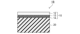
- FIG. 2 is a schematic cross-sectional view showing a metal laminate according to another embodiment of the present invention.
- 1 is a schematic cross-sectional view showing a metal laminate material having a chromate treatment layer according to one embodiment of the present invention.
- FIG. 2 is a schematic cross-sectional view showing a metal laminate having a chromate treatment layer according to another embodiment of the present invention.
- the cross-sectional views of the metal laminate materials of Example 1 and Comparative Examples 2 and 3 showing the presence or absence of voids at the bonding interface are shown.
- the present invention relates to a metal laminate material in which a metal layer consisting of at least one layer including a metal foil is laminated on at least one surface of a low dielectric film.
- the metal laminate material of the present invention includes a low dielectric film having a metal layer laminated on one surface thereof, and a low dielectric film having a metal layer laminated on both surfaces thereof.
- the metal contained at the interface between the low dielectric film and the metal layer is made of a non-magnetic metal, and no ferromagnetic metal is present at the interface. Therefore, the metal laminate material has excellent high frequency characteristics, and the low dielectric film and the metal layer have sufficient adhesion.
- FIG. 1 is a schematic cross-sectional view showing a metal laminated material according to one embodiment of the present invention. As shown in Fig. 1, the metal laminated material 1A has a metal layer 10 made of a metal foil laminated on one surface of a low dielectric film 20.
- FIG 2 is a schematic cross-sectional view showing another embodiment of a metal laminate of the present invention.
- a carrier-attached metal foil having an extremely thin metal layer, a release layer, and a carrier layer is used as the metal foil.
- the metal laminate 1B of the present invention has a metal layer 10 made of a carrier-attached metal foil laminated on one surface of a low dielectric film 20.
- the metal layer 10 is laminated in the order of extremely thin metal layer 14, release layer 13, and carrier layer 12 from the low dielectric film 20 side.
- the low-dielectric film may be made of any low-dielectric polymer material that can be used as a flexible substrate, such as a material with a relative dielectric constant ⁇ r of 3.3 or less and a dielectric loss tangent tan ⁇ of 0.006 or less, but is not limited thereto.
- the low-dielectric film may be appropriately selected from materials such as liquid crystal polymer, polyethylene fluoride (fluorine-based resin such as polytetrafluoroethylene), polyamide, isocyanate compound, polyamideimide, polyimide, low-dielectric constant polyimide, polyethylene terephthalate, polyetherimide, and cycloolefin polymer.
- the low-dielectric film is a liquid crystal polymer, polyethylene fluoride, polyamide, or low-dielectric constant polyimide, and more preferably, a liquid crystal polymer.
- the low-dielectric film is a single-layer film or a laminate consisting of multiple layers, and in the case of a multiple-layer film, at least one of the multiple layers may be a layer consisting of the low-dielectric polymer material. Layers other than the layer consisting of the low-dielectric polymer material may be made of various conventionally known materials such as epoxy resin.
- the liquid crystal polymer refers to an aromatic polyester resin having a basic structure such as parahydroxybenzoic acid, which exhibits liquid crystal properties in a molten state.
- the thickness of the low dielectric film can be appropriately set according to the application of the metal laminate.
- the thickness is usually 10 ⁇ m to 150 ⁇ m, preferably 25 ⁇ m to 150 ⁇ m, more preferably 25 ⁇ m to 120 ⁇ m, and particularly preferably 25 ⁇ m to 100 ⁇ m.
- the thickness of the low dielectric film refers to the average value of the values obtained by taking an optical microscope photograph of the cross section of the metal laminate and measuring the thickness of the low dielectric film at any 10 points on the optical microscope photograph.
- the thickness of the low dielectric film before bonding can be measured with a micrometer or the like, and refers to the average value of the thickness measured at 10 points randomly selected from the surface of the target low dielectric film.
- the deviation from the average value of the measured values at 10 points is preferably within 20% for all measured values, more preferably within 10%.
- the metal layer is not particularly limited as long as it contains a metal foil, and may be made of the metal foil or may further include another layer in addition to the metal foil. When the metal layer has another layer in addition to the metal foil, it is preferable that the other layer is between the low dielectric film and the metal foil.
- the metal foil is preferably a rolled metal foil, a metal foil with a carrier, or an electrolytic metal foil, and more preferably a rolled copper foil, a copper foil with a carrier, or an electrolytic copper foil.
- the metal foil may be a single-layer foil or a laminated foil of these.
- the type of metal constituting the metal foil varies depending on the application of the metal laminate material and is not particularly limited, but examples include copper, iron, nickel, zinc, tin, chromium, gold, silver, platinum, cobalt, titanium, and alloys thereof.
- Metal foils made of non-magnetic metals such as copper, zinc, tin, chromium, gold, silver, platinum, and titanium are preferred as the metal foil, and copper foil or copper alloy foil is particularly preferred.
- the copper alloy foil referred to here is one made of copper and a non-magnetic metal. This is because, for example, a flexible substrate for forming fine wiring can be obtained by rolling and joining these with a low dielectric film.
- the metals constituting the metal foil include ferromagnetic metals such as iron, nickel, cobalt, and alloys thereof
- ferromagnetic metals such as iron, nickel, cobalt, and alloys thereof
- non-magnetic metals include copper, zinc, tin, chromium, gold, silver, platinum, and titanium.
- the thickness of the metal foil is not particularly limited because it varies depending on the application of the metal laminate material.
- the thickness is preferably 3 ⁇ m to 100 ⁇ m, more preferably 10 ⁇ m to 50 ⁇ m, and particularly preferably 10 ⁇ m to 35 ⁇ m.
- the thickness of the nonmagnetic metal layer composed on the upper layer of the surface on the low dielectric film side of the metal foil is preferably 1.3 ⁇ m to 50 ⁇ m, more preferably 1.3 ⁇ m to 15 ⁇ m, and particularly preferably 1.5 ⁇ m to 10 ⁇ m.
- the thickness of the metal foil or nonmagnetic metal layer refers to the average value obtained by taking an optical microscope photograph of the cross section of the metal laminate material, measuring the thickness of the metal foil or nonmagnetic metal layer at any 10 points on the optical microscope photograph.
- the rolled copper foil is not particularly limited, but examples thereof include HA-V2 manufactured by JX Nippon Mining Co., Ltd. and C1020R-H manufactured by Mitsui Sumitomo Metal Mining Co., Ltd.
- the electrolytic copper foil is not particularly limited, but examples thereof include CF-PLFA manufactured by Fukuda Metal Foil and Powder Co., Ltd.
- metal foil with a carrier having an extremely thin metal layer, a release layer, and a carrier layer as the metal foil.
- the metal foil with a carrier is laminated in the order of extremely thin metal layer, release layer, and carrier layer from the low dielectric film side, as shown in Figure 2.
- metal foil with a carrier the "metal foil" in the resulting metal laminate material refers to the portion consisting of the extremely thin metal layer, release layer, and carrier layer.
- the carrier layer of the carrier-attached metal foil has a sheet shape and functions as a support material or protective layer to prevent wrinkles or folds in the metal laminate and scratches on the ultra-thin metal layer.
- the carrier layer include foils or plates made of copper, aluminum, nickel, and their alloys (stainless steel, brass, etc.), resins with a metal coating on the surface, etc.
- the carrier layer is preferably copper foil.
- the thickness of the carrier layer is not particularly limited, but is, for example, 10 ⁇ m or more and 100 ⁇ m or less.
- the release layer of the carrier-attached metal foil reduces the peel strength of the carrier layer and also has the function of suppressing mutual diffusion that may occur between the carrier layer and the ultrathin metal layer due to heat treatment.
- the release layer may be either an organic release layer or an inorganic release layer, and examples of components used in the organic release layer include nitrogen-containing organic compounds, sulfur-containing organic compounds, and carboxylic acids.
- nitrogen-containing organic compounds include triazole compounds and imidazole compounds.
- triazole compounds include 1,2,3-benzotriazole, carboxybenzotriazole, N',N'-bis(benzotriazolylmethyl)urea, 1H-1,2,4-triazole, and 3-amino-1H-1,2,4-triazole.
- Examples of sulfur-containing organic compounds include mercaptobenzothiazole, thiocyanuric acid, and 2-benzimidazolethiol.
- Examples of carboxylic acids include monocarboxylic acids and dicarboxylic acids.
- examples of components used in the inorganic release layer include Ni, Mo, Co, Cr, Fe, Ti, W, P, Zn, chromate-treated films, etc.
- the thickness of the release layer is usually 1 nm or more and 1 ⁇ m or less, and preferably 5 nm or more and 500 nm or less.
- the metal constituting the ultra-thin metal layer of the carrier-attached metal foil varies depending on the application of the metal laminate material and is not particularly limited, but examples include copper, zinc, tin, chromium, gold, silver, platinum, titanium, and alloys thereof.
- the ultra-thin metal layer is preferably a layer of copper or a copper alloy.
- the thickness of the ultra-thin metal layer is usually 1.5 ⁇ m or more and 10 ⁇ m or less, and preferably 1.5 ⁇ m or more and 7 ⁇ m or less.
- the carrier-attached metal foil is preferably one in which the carrier layer and the ultra-thin metal layer are made of copper or a copper alloy, and more preferably a carrier-attached copper foil in which both are copper.
- the metal layer may have a chromate treatment layer between the low dielectric film and the metal foil.
- the metal foil is an electrolytic metal foil or a metal foil with a carrier
- the metal layer preferably has a chromate treatment layer between the low dielectric film and the metal foil.
- the chromate treatment layer can function as an anti-rust layer.
- the chromate treatment layer is preferably formed on the surface of the metal foil. In particular, when the metal layer is a metal foil surface having a chromate treatment layer and a low dielectric film is laminated, this is preferable because it can further increase the adhesion between the metal layer and the low dielectric film.
- the chromate treatment layer is preferably in contact with the surfaces of both the low dielectric film and the metal foil.
- the thickness of the chromate treatment layer is usually more than 0 nm and not more than 20 nm, and preferably 1 nm or more and not more than 10 nm.
- methods for measuring the thickness of the chromate treatment layer include, but are not limited to, thickness measurements using X-ray photoelectron spectroscopy (XPS) or Auger electron spectroscopy (AES).
- the chromate treatment layer refers to a layer formed using a solution containing chromic anhydride, chromic acid, dichromate, or dichromate (also called a chromate treatment solution).
- the chromate treatment layer is preferably made of chromate.
- Figure 3 is a schematic cross-sectional view showing a metal laminate material having a chromate treatment layer according to one embodiment of the present invention.
- the metal laminate material 1C of the present invention has a metal layer 10 laminated on one surface of a low dielectric film 20.
- the metal laminate material 1C has a chromate treatment layer 15 between the low dielectric film 20 and the metal foil 11.
- the chromate treatment layer 15 is in contact with the surfaces of both the low dielectric film 20 and the metal foil 11.
- the metal laminate material 1C is laminated in the order of the low dielectric film 20, the chromate treatment layer 15, and the metal foil 11.
- FIG. 4 is a schematic cross-sectional view showing a metal laminate having a chromate treatment layer according to another embodiment of the present invention.
- a carrier-attached metal foil having an extremely thin metal layer, a peeling layer, and a carrier layer is used as the metal foil.
- the metal laminate 1D of the present invention has a metal layer 10 laminated on one surface of a low dielectric film 20.
- the metal laminate 1D has a chromate treatment layer 15 between the low dielectric film 20 and a metal foil 11 having an extremely thin metal layer 14, a peeling layer 13, and a carrier layer 12.
- the chromate treatment layer 15 is in contact with both the surfaces of the low dielectric film 20 and the metal foil 11.
- the metal laminate 1D is laminated in the order of the low dielectric film 20, the chromate treatment layer 15, the extremely thin metal layer 14, the peeling layer 13, and the carrier layer 12.
- the metal laminate material may have an organic layer, such as a treatment layer with a silane coupling agent, on the surface of the metal layer on the low dielectric film side.
- silane coupling agents include, but are not limited to, olefin-based silanes, epoxy-based silanes, acrylic-based silanes, amino-based silanes, and mercapto-based silanes.
- the silane coupling agent may be applied by spraying, applying with a coater, immersing, or other suitable method.
- the metal laminate material may also have a treatment layer with a benzotriazole (BTA) compound on the surface of the metal layer on the low dielectric film side.
- BTA benzotriazole
- the metal laminate preferably does not have an organic layer such as a treatment layer with a silane coupling agent or a benzotriazole compound on the surface of the metal layer on the low dielectric film side.
- the silicon (Si) content on the surface of the metal layer on the low dielectric film side is preferably 0.03 ⁇ g/cm 2 or less, more preferably 0.025 ⁇ g/cm 2 or less.
- the Si content can be measured, for example, by fluorescent X-ray analysis.
- the metal laminate preferably does not have a roughened particle layer or a heat-resistant layer on the surface of the metal foil.
- These layers usually contain ferromagnetic metals such as Ni and Co, and the presence of ferromagnetic metals at the lamination interface of the metal laminate would degrade the high-frequency characteristics of the metal laminate.
- the roughened particle layer contains, for example, any one metal selected from the group consisting of Cu, Co, and Ni, or an alloy thereof, and specific examples thereof include a cobalt-nickel alloy plating layer, a copper-cobalt-nickel alloy plating layer, etc.
- the heat-resistant layer contains, for example, any one metal selected from the group consisting of Co, Ni, and Mo, or an alloy thereof, and specific examples thereof include a Ni plating layer, etc.
- the metal laminate of the present invention has excellent high frequency characteristics because no ferromagnetic metal (also called high magnetic permeability metal) is present at the interface between the low dielectric film and the metal layer, i.e., the metal contained at the interface between the low dielectric film and the metal layer is a non-magnetic metal.
- no ferromagnetic metal also called high magnetic permeability metal
- the analysis of the components contained in the interface between the low dielectric film and the metal layer can be performed, for example, by glow discharge optical emission surface analysis (GDS).
- GDS glow discharge optical emission surface analysis
- the components contained in the range of 1.3 ⁇ m or less from the surface of the metal layer on the low dielectric film side toward the metal layer side can be measured, for example, by GDS. Therefore, in the metal laminate material of the present invention, at the interface between the low dielectric film and the metal layer, the metal contained in the range of 1.3 ⁇ m or less from the surface of the metal layer on the low dielectric film side toward the metal layer side (in the thickness direction) is made of a non-magnetic metal.
- GDS is an analytical technique that performs elemental analysis in the depth direction of a sample, and is a destructive analysis using sputtering.
- analysis of components contained in the interface can also be performed using X-ray photoelectron spectroscopy (XPS).
- XPS X-ray photoelectron spectroscopy
- non-magnetic metal refers to metals other than ferromagnetic metals (e.g., iron, nickel, cobalt, etc.).
- ferromagnetic metals are also called high magnetic permeability metals, and refer to, for example, metals with a relative magnetic permeability of 10.0 or more.
- the relative magnetic permeability of non-magnetic metals is, for example, 1.5 or less.
- non-magnetic metals include copper, zinc, tin, chromium, gold, silver, platinum, and titanium, and among these, copper or chromium is preferred.
- the non-magnetic metals present at the lamination interface of the metal laminate material are copper and chromium. In one embodiment, iron, nickel, and cobalt are not present at the lamination interface of the metal laminate material.
- the non-magnetic metal contained within a range of 1.3 ⁇ m or less from the surface of the low dielectric film side of the metal layer toward the metal layer side is preferably a single layer (one layer).
- the metal layer composed of a non-magnetic metal is a single layer composed of metal foil (excluding the chromate treatment layer). It is considered that a single layer configuration provides better high-frequency characteristics and suppresses voids at the bonding interface between the metal layer and the low dielectric film.
- the metal layer has two or more layers composed of a non-magnetic metal (for example, a metal layer/metal foil composition composed of a non-magnetic metal) within a range of 1.3 ⁇ m or less from the surface of the low dielectric film side toward the metal layer side, voids may occur at the lamination interface between each metal layer during bonding, which is undesirable because it is possible that swelling may occur during the solder reflow process when applied to a printed wiring board.
- a non-magnetic metal for example, a metal layer/metal foil composition composed of a non-magnetic metal
- the metal laminate of the present invention has a peel strength between the low dielectric film and the metal layer of 1.0 N/cm or more, preferably 3.0 N/cm or more, and more preferably 5.0 N/cm or more.
- a peel strength of 1.0 N/cm or more can improve the reliability of the fine wiring of the printed wiring board.
- a test piece is first prepared from the metal laminate, and a 1 cm wide cut is made in the metal layer using a knife or the like. After the metal layer and the low dielectric film are partially peeled off, the low dielectric film is fixed to a support, and the metal layer is pulled in a 90° direction to the low dielectric film at a speed of 50 mm/min. The force required to peel it off at this time is taken as the peel strength (unit: N/cm). If the metal layer is thin and brittle, it may break when measuring the peel strength.
- the surface of the metal layer may be electrolytically plated (for example, copper plating when the metal layer is copper) to increase the thickness of the metal layer to about 5 ⁇ m to about 50 ⁇ m, and then the peel strength may be measured.
- the method for measuring the peel strength is specified in JIS C6471.
- peel strength between a low dielectric film and a metal layer refers to the peel strength when peeling occurs at the interface between the low dielectric film and the metal layer, as well as the peel strength when peeling occurs due to internal destruction of the metal layer and the peel strength when peeling occurs due to internal destruction of the low dielectric film.
- a chromate treatment layer or a treatment layer using a silane coupling agent or a benzotriazole compound is laminated between the low dielectric film and the metal foil, in addition to the peel strength when peeling occurs at the interface between the low dielectric film and the treatment layer, it also refers to the peel strength when peeling occurs at the interface between the metal foil and the treatment layer and the peel strength when peeling occurs due to internal destruction of the treatment layer.
- the metal laminate of the present invention has a smooth lamination interface and therefore has superior high frequency characteristics compared to conventional metal laminates produced by thermal lamination.
- the smoothness of the lamination interface of the metal laminate can be confirmed by measuring the surface roughness of the surface on the metal layer side of the low dielectric film. For example, after removing the metal layer from the metal laminate by etching or the like, the surface (bonding surface) of the low dielectric film can be measured in accordance with ISO25178 using an atomic force microscope (AFM).
- AFM atomic force microscope
- the metal laminate of the present invention has an arithmetic mean height Sa of the surface on the metal layer side of the low dielectric film, measured in accordance with ISO 25178, of preferably 60 nm or less, more preferably 50 nm or less, and particularly preferably 20 nm or less.
- the metal laminate of the present invention has a maximum height Sz of the surface on the metal layer side of the low dielectric film, measured in accordance with ISO 25178, of preferably 700 nm or less, more preferably 600 nm or less, even more preferably 450 nm or less, and particularly preferably 300 nm or less.
- the metal laminate of the present invention has a developed surface area ratio Sdr of the surface on the metal layer side of the low dielectric film, measured in accordance with ISO25178, of preferably 35% or less, more preferably 10% or less, even more preferably 5% or less, and particularly preferably 1.5% or less.
- the present invention also relates to a manufacturing method of the metal laminate.
- the metal laminate of the present invention can be manufactured by a surface activation bonding method. Since a strong bond is formed at the bonding interface by the surface activation treatment, the adhesion of the interface can be ensured even if a ferromagnetic metal such as Ni or Co is not present at the interface. In addition, the adhesion of the lamination interface can be ensured without relying on the physical anchor effect of roughening particles as in the case of a metal laminate manufactured by a thermal lamination method. Furthermore, by manufacturing by the surface activation bonding method, the metal foil can be laminated on the low dielectric film while maintaining the smoothness of its surface. From these points, the metal laminate has excellent high frequency characteristics and adhesion of the lamination interface.
- the method for manufacturing a metal laminate of the present invention includes the steps of preparing a low dielectric film and a metal foil (step 1), activating at least one surface of the low dielectric film by sputter etching (step 2-1), activating the surface of the metal foil by sputter etching (step 2-2), and rolling-bonding the activated surfaces of the low dielectric film and the metal foil together at a rolling reduction of 0 to 30% (step 3).
- steps 1, 2 (steps 2-1 and 2-2), and 3 are performed sequentially, but steps 2-1 and 2-2 can be performed simultaneously or sequentially.
- step 1 a low dielectric film and a metal foil are prepared.
- the low dielectric film and the metal foil those described above for the metal laminate can be used.
- a metal foil having no ferromagnetic metal on the surface preferably having no roughening treatment layer on the surface, when the metal foil and the low dielectric film are laminated, a metal laminate having no ferromagnetic metal at the lamination interface can be obtained.
- step 2-1 Surface activation step of low dielectric film
- the sputter etching process can be performed, for example, by preparing a low dielectric film as a long coil with a width of 100 mm to 600 mm, using the joint surface of the low dielectric film as one electrode grounded to earth, applying an AC current of 1 MHz to 50 MHz between the low dielectric film and the other electrode supported insulated to generate a glow discharge, and setting the area of the electrode exposed to the plasma generated by the glow discharge to 1/3 or less of the area of the other electrode.
- the earthed electrode takes the form of a cooling roll to prevent the temperature of the transported material from increasing.
- the surface to be joined of the low dielectric film is sputtered under vacuum with an active gas or an inert gas to completely remove any adsorbed matter on the surface.
- an active gas oxygen or a mixed gas containing oxygen can be used.
- oxygen or a mixed gas containing oxygen can be used.
- the inert gas argon, neon, xenon, krypton, nitrogen, etc., or a mixed gas containing at least one of these can be used.
- Oxygen is preferred as the gas used in the sputter etching process of the low dielectric film.
- oxygen By using oxygen, functional groups such as carboxyl groups and hydroxyl groups can be added to the surface of the low dielectric film, and the adhesion between the low dielectric film and the metal layer can be improved compared to when an inert gas such as argon or nitrogen is used.
- the treatment conditions for sputter etching can be appropriately set, and for example, sputter etching can be performed under vacuum with a plasma output of 100 W to 10 kW and a line speed of 0.5 m/min to 30 m/min. Even when oxygen gas is used, the treatment conditions for sputter etching are, for example, under vacuum with a plasma output of 100 W to 10 kW and a line speed of 0.5 m/min to 30 m/min.
- the degree of vacuum is preferably high in order to prevent re-adsorption onto the surface, and may be, for example, 1 ⁇ 10 ⁇ 5 Pa to 10 Pa.
- step 2-2 Metal Foil Surface Activation Step
- the surface of the metal foil is activated by sputter etching.
- the sputter etching process in the surface activation process can be carried out, for example, by preparing the metal foil to be joined as a long coil with a width of 100 mm to 600 mm, using the joining surface of the metal foil as one electrode grounded to earth, and applying an alternating current of 1 MHz to 50 MHz between it and the other electrode that is insulated and supported to generate a glow discharge, with the area of the electrode exposed to the plasma generated by the glow discharge being 1/3 or less of the area of the other electrode.
- the earthed electrode takes the form of a cooling roll to prevent the temperature of the transported material from rising.
- the surface to be joined of the metal foil is sputtered with an inert gas under vacuum to completely remove the adsorbed matter on the surface and to remove part or all of the oxide layer on the surface. It is preferable to completely remove the oxide layer.
- an inert gas argon, neon, xenon, krypton, etc., or a mixed gas containing at least one of these can be applied, but argon is preferable.
- the adsorbed matter on the surface of the metal foil can be completely removed with an etching amount of about 1 nm, and in particular, the oxide layer of copper can usually be removed with an etching amount of about 5 nm to 12 nm ( SiO2 equivalent).
- the treatment conditions for sputter etching can be appropriately set depending on the type of metal foil, etc. For example, it can be performed under vacuum with a plasma output of 100 W to 10 kW and a line speed of 0.5 m/min to 30 m/min.
- the degree of vacuum at this time is preferably high in order to prevent re-adsorption onto the surface, but a value of 1 ⁇ 10 ⁇ 5 Pa to 10 Pa will suffice.
- the surface of the metal foil before activation by sputter etching may be subjected to a chromate treatment, a silane coupling agent treatment, a treatment with a benzotriazole compound, or the like. That is, a metal foil having a chromate treatment layer, a silane coupling agent treatment layer, or a benzotriazole compound treatment layer on the surface can be used.
- a treatment layer is provided on the surface of the metal foil, the surface of the treatment layer is activated by sputter etching. At that time, the treatment layer may be completely removed by sputter etching, or may remain without being removed.
- an organic layer such as a silane coupling agent treatment layer or a benzotriazole compound treatment layer is removed from the surface of the metal foil by sputter etching.
- the amount of etching is usually 1 nm to 100 nm.
- a chromate treatment layer is provided on the surface of the metal foil before activation by sputter etching, it is preferable to activate the surface by sputter etching so that the treatment layer remains, since this can increase the adhesion when bonding with the above-mentioned low dielectric film.
- the low dielectric film and the metal foil are firmly bonded, which is preferable because it can significantly increase adhesion.
- step 3 the pressure bonding (rolling bonding) between the surfaces activated by sputter etching can be performed by roll bonding.
- the rolling wire load of the roll bonding is not particularly limited, and can be set to, for example, a range of 0.1 tf/cm to 10 tf/cm.
- the rolling wire load is not limited to this numerical range.
- the rolling wire load is too high, not only the surface layer of the low dielectric film or metal foil but also the bonding interface is likely to deform, so that the thickness accuracy of each layer in the metal laminate material may decrease.
- the rolling wire load is high, the processing strain applied during bonding may be large.
- the reduction ratio during roll bonding is 0 to 30%, preferably 0 to 15%.
- the above-mentioned surface activated bonding method allows the reduction ratio to be low, so a metal layer with excellent thickness precision can be formed without wrinkles or cracks. Furthermore, since the waviness at the interface between the metal foil and the low dielectric film can be reduced, when wiring is formed by pattern etching of the metal foil, precise wiring can be obtained due to excellent thickness precision.
- the temperature during roll bonding is, for example, 15°C to 100°C, preferably 15°C to 60°C, and more preferably room temperature.
- Joining by roll pressure is preferably performed in a non-oxidizing atmosphere, such as a vacuum atmosphere or an inert gas atmosphere such as Ar, to prevent a decrease in adhesion at the laminate interface due to re-adsorption of oxygen to the metal foil.
- a non-oxidizing atmosphere such as a vacuum atmosphere or an inert gas atmosphere such as Ar
- the metal laminate obtained by pressure welding can be further heat-treated as necessary, and preferably is.
- Heat treatment removes distortion in the metal layer and improves adhesion between the layers.
- the heat treatment temperature can be in the range of -150°C to the melting point of the low dielectric film +10°C.
- the temperature is 150°C to 350°C, preferably 160°C to 340°C, and more preferably 260°C to 340°C.
- the atmosphere in which the heat treatment is performed is not particularly limited, but a vacuum atmosphere or an inert gas atmosphere such as N2 or Ar is preferable, because this can prevent the metal layer from being oxidized by the heat treatment and the adhesion between the metal layer and the low dielectric film from decreasing.
- the time for the heat treatment is not particularly limited as long as it can sufficiently increase the adhesion between the metal layer and the low dielectric film.
- the soaking time is preferably 0 to 25,200 seconds, more preferably 0 to 18,000 seconds, and particularly preferably 180 to 15,000 seconds.
- the time at or above the lower limit of these ranges sufficient adhesion between the metal layer and the low dielectric film can be ensured, and by setting the time at or below the upper limit of these ranges, high production efficiency and low cost of the metal laminate material can be achieved. Note that even if the soaking time mentioned above is 0 seconds (i.e., cooling is performed immediately after reaching the target temperature without a soaking time), it is possible to sufficiently increase the adhesion between the metal layer and the low dielectric film.
- the method of performing the heat treatment includes, for example, a method of maintaining the metal laminate material at a desired heat treatment temperature for a desired time in a desired atmosphere (for example, a vacuum atmosphere or an inert gas atmosphere such as N 2 or Ar) using a batch heat treatment furnace.
- a desired atmosphere for example, a vacuum atmosphere or an inert gas atmosphere such as N 2 or Ar
- the heat treatment may be performed by a roll-to-roll method using a continuous heat treatment furnace.
- At least the heating part and the cooling part in the continuous heat treatment furnace are set to a desired atmosphere (for example, a vacuum atmosphere or an inert gas atmosphere such as N 2 or Ar) and maintained at a desired temperature, and the metal laminate material is passed through the heating part and the cooling part at a desired speed to maintain the metal laminate material at the desired heat treatment temperature for a desired time.
- a desired atmosphere for example, a vacuum atmosphere or an inert gas atmosphere such as N 2 or Ar
- the metal laminate of the present invention can be utilized as a metal-clad laminate for producing a flexible printed circuit board.
- the metal laminate of the present invention can be used to obtain a printed wiring board with fine wiring formed thereon.
- the present invention also relates to a printed wiring board in which a circuit is formed on a metal laminate.
- an additional metal layer can be formed only on the wiring portion.
- a printed wiring board can be obtained by appropriately using a conventionally known method such as the modified semi-additive method (MSAP method), the semi-additive method (SAP method), or the subtractive method.
- a printed wiring board can be manufactured by masking the non-wiring portion on the metal layer of the metal laminate, forming an additional metal layer by copper plating or the like on the unmasked portion, removing the mask, and removing the metal layer hidden by the mask by etching.
- the "printed wiring board” in the present invention includes not only a laminate with wiring formed thereon, but also a board on which electronic components such as ICs are mounted after wiring is formed.
- a metal laminate material is described in which a metal layer is laminated on one surface of a low dielectric film, but the metal laminate material is not limited to this. In other words, if necessary, metal layers may be provided on both surfaces of the low dielectric film.
- a metal laminate material in which metal layers are provided on both surfaces of a low dielectric film, a flexible printed circuit board in which wiring is formed on both surfaces of the low dielectric film can be obtained.
- Example 1 A liquid crystal polymer film having a thickness of 50 ⁇ m (Vexstar CTQ manufactured by Kuraray Co., Ltd.) was prepared, and a 12 ⁇ m thick electrolytic copper foil (CF-PLFA manufactured by Fukuda Metal Foil and Powder Co., Ltd.) having a chromate treatment layer on the surface and made of copper was prepared as the metal foil.
- Vexstar CTQ manufactured by Kuraray Co., Ltd.
- CF-PLFA electrolytic copper foil having a chromate treatment layer on the surface and made of copper
- Example 1 Example 1 (layer structure: electrolytic copper foil / liquid crystal polymer film).
- Example 2 A liquid crystal polymer film having a thickness of 50 ⁇ m (Vexstar CTQ manufactured by Kuraray Co., Ltd.) was prepared, and a rolled copper foil having a thickness of 12 ⁇ m and made of copper having a benzotriazole compound treatment layer (organic layer) on the surface was prepared as the metal foil (HA-V2 manufactured by JX Metals Co., Ltd.).
- one surface of the liquid crystal polymer film was activated by sputter etching with O 2 gas (etching amount 300 nm), and the surface of the rolled copper foil was activated by completely removing the treatment layer by sputter etching with Ar gas (etching amount 2 nm), and the activated surfaces of the liquid crystal polymer film and the rolled copper foil were rolled and bonded with a line load of 1.5 tf / cm to produce a metal laminate material.
- the rolling reduction rate was 2.0%.
- the metal laminate material was subjected to a heat treatment at 310 ° C. to obtain a metal laminate material of Example 2 (layer structure: rolled copper foil / liquid crystal polymer film).
- Example 3 A 25 ⁇ m thick liquid crystal polymer film (Vexstar CTQ manufactured by Kuraray Co., Ltd.) was prepared, and a 18 ⁇ m thick rolled copper foil (C1020R-H manufactured by Mitsui Sumitomo Metal Mining Co., Ltd.) was prepared. One surface of the liquid crystal polymer film was activated by sputter etching with Ar gas (etching amount 10 nm). The same procedure as in Example 2 was followed to obtain a metal laminate material (layer structure: rolled copper foil/liquid crystal polymer film) of Example 3.
- Example 4 A metal laminate material (layer structure: rolled copper foil / liquid crystal polymer film) of Example 4 was obtained in the same manner as in Example 3, except that one surface of the liquid crystal polymer film was activated by sputter etching (etching amount 140 nm) with N2 gas.
- Comparative Example 1 A metal laminate material (layer structure: electrolytic copper foil/liquid crystal polymer film) of Comparative Example 1 was obtained in the same manner as in Example 1, except that an electrolytic copper foil having a thickness of 12 ⁇ m and having a surface with an anticorrosive layer containing Co or the like (CF-T9DA-SV manufactured by Fukuda Metal Foil and Powder Co., Ltd.) was used as the electrolytic copper foil.
- an electrolytic copper foil having a thickness of 12 ⁇ m and having a surface with an anticorrosive layer containing Co or the like CF-T9DA-SV manufactured by Fukuda Metal Foil and Powder Co., Ltd.
- Example 2 A liquid crystal polymer film having a thickness of 25 ⁇ m (Vexstar CTQ manufactured by Kuraray Co., Ltd.) was prepared, and a rolled copper foil having a thickness of 18 ⁇ m (HA-V2 manufactured by JX Metals Co., Ltd.) was prepared as the metal foil. Next, one surface of the liquid crystal polymer film was activated by sputter etching with O 2 gas (etching amount 300 nm), and then a 5 nm NiCr alloy sputter layer was sputter-formed as a base layer on the activated surface, and a 10 nm Cu sputter layer was sputter-formed as an upper layer to form a metal layer.
- O 2 gas etching amount 300 nm
- the surface of the metal layer and the surface of the rolled copper foil were activated by sputter etching with Ar gas (etching amount: metal layer 2 nm, rolled copper foil 2 nm), and the activated surfaces of the metal layer and the rolled copper foil were roll-bonded with a line load of 1.5 tf/cm to produce a metal laminate.
- the rolling reduction was 2.3%.
- the metal laminate was subjected to a heat treatment at 300° C. to obtain a metal laminate of Comparative Example 2 (layer structure: rolled copper foil/metal layer/liquid crystal polymer film).
- Example 3 A liquid crystal polymer film having a thickness of 25 ⁇ m (Vexstar CTQ manufactured by Kuraray Co., Ltd.) was prepared, and a rolled copper foil having a thickness of 18 ⁇ m (HA-V2 manufactured by JX Metals Co., Ltd.) was prepared as the metal foil. Next, one surface of the liquid crystal polymer film was activated by sputter etching with O 2 gas (etching amount 300 nm), and then a 28 nm NiCr alloy sputter layer was sputter-deposited on the activated surface to form a metal layer.
- O 2 gas etching amount 300 nm
- the surface of the metal layer and the surface of the rolled copper foil were activated by sputter etching with Ar gas (etching amount: metal layer 2 nm, rolled copper foil 2 nm), and the activated surfaces of the metal layer and the rolled copper foil were roll-bonded with a line load of 1.5 tf/cm to produce a metal laminate.
- the rolling reduction rate was 2.3%.
- the metal laminate was subjected to a heat treatment at 300 ° C. to obtain a metal laminate of Comparative Example 3 (layer structure: rolled copper foil / metal layer / liquid crystal polymer film).
- Comparative Example 4 By a thermal lamination method, an 18 ⁇ m-thick electrolytic copper foil having a treatment layer made of a roughening particle layer or the like on one side was thermocompressed to both surfaces of a 50 ⁇ m-thick liquid crystal polymer film (Vexstar CTQ manufactured by Kuraray Co., Ltd.) at a temperature of 310° C. or higher to produce a metal laminate material of Comparative Example 4 (layer structure: electrolytic copper foil (roughened)/liquid crystal polymer film/electrolytic copper foil (roughened)).
- a 50 ⁇ m-thick liquid crystal polymer film Vexstar CTQ manufactured by Kuraray Co., Ltd.
- GDS measurement device High-frequency glow discharge optical emission spectrometer (Horiba, GD-Profiler 2) Excitation mode: Normal Light source pressure: 600 Pa Light source output: 30W Anode diameter: 4 mm
- the transmission line was a single-ended microstrip transmission line with a wiring height of 25 ⁇ m, width of 110 ⁇ m, and length of 100 mm. Measurements were performed at a frequency of 40 GHz using a network analyzer N5227B (Keysight Technologies, Inc.). Note that in Examples 1-2 and Comparative Examples 1-2, a microstrip line was created on the laminated copper foil side and measurements were performed.
- Table 1 shows the configurations and evaluation results of the metal laminate materials of Examples 1 to 4 and Comparative Examples 1 to 4.
- LCP stands for liquid crystal polymer film.
- the metal laminates of Examples 1 and 2 which do not have a ferromagnetic metal at the lamination interface of the metal laminate, had smaller transmission loss (S21) at high frequencies and superior high frequency transmission characteristics compared to the metal laminates of Comparative Examples 1 to 2 and 4, which have a ferromagnetic metal (Ni, Co) at the lamination interface of the metal laminate.
- the metal laminates of Examples 1 and 2 when compared to Comparative Example 4, which has a roughened particle layer, the metal laminates of Examples 1 and 2 have a smoother interface and no ferromagnetic metal at the lamination interface, so it was confirmed that the metal laminates of Examples 1 and 2 have smaller transmission loss (S21) at high frequencies and superior high frequency transmission characteristics.
- the metal laminate of Examples 1 to 4 had sufficient peel strength, although the ferromagnetic metal that contributes to the adhesion of the laminate interface was not present at the interface and the interface was smooth. This is thought to be because in the metal laminate of Examples 1 to 4, a strong bond is formed at the interface between the liquid crystal polymer film and the copper foil by the surface activation treatment, so that the adhesion of the laminate interface can be ensured without relying on the physical anchor effect of the roughening particles.
- the metal laminate of Examples 1 and 2 in which the surface of the liquid crystal polymer film was activated by sputter etching with O 2 gas, had a stronger bond between the interface of the liquid crystal polymer film and the copper foil and had excellent peel strength, compared to the metal laminate of Examples 3 and 4, in which the surface of the liquid crystal polymer film was activated by sputter etching with Ar gas or N 2 gas.
- Example 1 which has a chromate treatment layer on the surface (liquid crystal polymer film side) of the metal foil of the metal laminate, has a stronger bond at the interface between the liquid crystal polymer film and the copper foil and has better peel strength than Example 2, which does not have a chromate treatment layer on the surface of the metal foil of the metal laminate.
- Table 1 shows the evaluation results of the metal laminate materials of Examples 1 to 4 and Comparative Examples 1 to 4, and Figure 5 shows cross-sectional views of the metal laminate materials of Example 1 and Comparative Examples 2 to 3 showing the presence or absence of voids at the bonding interface.
- the metal laminate materials of Examples 1 to 4 in which the metal contained within a range of 1.3 ⁇ m or less from the surface of the low dielectric film side of the metal layer toward the metal layer side is a single layer (one layer), have no voids at the bonding interface, and it was confirmed that they can be suitably used in the solder reflow process when applied as a printed wiring board.
- the metal laminate materials of Comparative Examples 2 to 3 in which the metal contained within a range of 1.3 ⁇ m or less from the surface of the low dielectric film side of the metal layer toward the metal layer side is composed of two or more layers (metal layer/copper foil), have voids at the bonding interface, and it was confirmed that there is a risk of swelling due to these voids during the solder reflow process when applied as a printed wiring board.
- the thickness of the sputtered layer (metal layer) was greater than in Comparative Example 2, resulting in more voids at the bonding interface.
Landscapes
- Engineering & Computer Science (AREA)
- Microelectronics & Electronic Packaging (AREA)
- Physics & Mathematics (AREA)
- Fluid Mechanics (AREA)
- Laminated Bodies (AREA)
Priority Applications (3)
| Application Number | Priority Date | Filing Date | Title |
|---|---|---|---|
| JP2025515201A JPWO2024219326A1 (https=) | 2023-04-19 | 2024-04-12 | |
| CN202480025670.0A CN120936492A (zh) | 2023-04-19 | 2024-04-12 | 金属层叠材料及其制造方法、印刷线路板 |
| KR1020257036864A KR20250172614A (ko) | 2023-04-19 | 2024-04-12 | 금속 적층재 및 그 제조 방법, 그리고 프린트 배선판 |
Applications Claiming Priority (2)
| Application Number | Priority Date | Filing Date | Title |
|---|---|---|---|
| JP2023068300 | 2023-04-19 | ||
| JP2023-068300 | 2023-04-19 |
Publications (1)
| Publication Number | Publication Date |
|---|---|
| WO2024219326A1 true WO2024219326A1 (ja) | 2024-10-24 |
Family
ID=93152366
Family Applications (1)
| Application Number | Title | Priority Date | Filing Date |
|---|---|---|---|
| PCT/JP2024/014800 Ceased WO2024219326A1 (ja) | 2023-04-19 | 2024-04-12 | 金属積層材及びその製造方法、並びにプリント配線板 |
Country Status (5)
| Country | Link |
|---|---|
| JP (1) | JPWO2024219326A1 (https=) |
| KR (1) | KR20250172614A (https=) |
| CN (1) | CN120936492A (https=) |
| TW (1) | TW202506405A (https=) |
| WO (1) | WO2024219326A1 (https=) |
Citations (6)
| Publication number | Priority date | Publication date | Assignee | Title |
|---|---|---|---|---|
| JP2002113811A (ja) * | 2000-10-11 | 2002-04-16 | Toyo Kohan Co Ltd | 多層金属積層フィルム及びその製造方法 |
| JP2005324467A (ja) * | 2004-05-14 | 2005-11-24 | Toyo Kohan Co Ltd | 低熱膨張積層材の製造方法および低熱膨張積層材を用いた部品の製造方法 |
| JP2007273679A (ja) * | 2006-03-31 | 2007-10-18 | Nikko Kinzoku Kk | プリント配線基板用銅又は銅合金箔 |
| WO2016174998A1 (ja) * | 2015-04-28 | 2016-11-03 | 三井金属鉱業株式会社 | 粗化処理銅箔及びプリント配線板 |
| WO2019244541A1 (ja) * | 2018-06-20 | 2019-12-26 | ナミックス株式会社 | 粗化処理銅箔、銅張積層板及びプリント配線板 |
| JP2021171963A (ja) * | 2020-04-22 | 2021-11-01 | 東洋鋼鈑株式会社 | 金属積層フィルム及びその製造方法 |
Family Cites Families (1)
| Publication number | Priority date | Publication date | Assignee | Title |
|---|---|---|---|---|
| KR101742978B1 (ko) | 2015-06-18 | 2017-06-05 | 주식회사 그린플러스 | 갑각류 양식시스템 |
-
2024
- 2024-04-11 TW TW113113552A patent/TW202506405A/zh unknown
- 2024-04-12 JP JP2025515201A patent/JPWO2024219326A1/ja active Pending
- 2024-04-12 KR KR1020257036864A patent/KR20250172614A/ko active Pending
- 2024-04-12 WO PCT/JP2024/014800 patent/WO2024219326A1/ja not_active Ceased
- 2024-04-12 CN CN202480025670.0A patent/CN120936492A/zh active Pending
Patent Citations (6)
| Publication number | Priority date | Publication date | Assignee | Title |
|---|---|---|---|---|
| JP2002113811A (ja) * | 2000-10-11 | 2002-04-16 | Toyo Kohan Co Ltd | 多層金属積層フィルム及びその製造方法 |
| JP2005324467A (ja) * | 2004-05-14 | 2005-11-24 | Toyo Kohan Co Ltd | 低熱膨張積層材の製造方法および低熱膨張積層材を用いた部品の製造方法 |
| JP2007273679A (ja) * | 2006-03-31 | 2007-10-18 | Nikko Kinzoku Kk | プリント配線基板用銅又は銅合金箔 |
| WO2016174998A1 (ja) * | 2015-04-28 | 2016-11-03 | 三井金属鉱業株式会社 | 粗化処理銅箔及びプリント配線板 |
| WO2019244541A1 (ja) * | 2018-06-20 | 2019-12-26 | ナミックス株式会社 | 粗化処理銅箔、銅張積層板及びプリント配線板 |
| JP2021171963A (ja) * | 2020-04-22 | 2021-11-01 | 東洋鋼鈑株式会社 | 金属積層フィルム及びその製造方法 |
Also Published As
| Publication number | Publication date |
|---|---|
| TW202506405A (zh) | 2025-02-16 |
| CN120936492A (zh) | 2025-11-11 |
| JPWO2024219326A1 (https=) | 2024-10-24 |
| KR20250172614A (ko) | 2025-12-09 |
Similar Documents
| Publication | Publication Date | Title |
|---|---|---|
| JP7588956B2 (ja) | キャリア層付き金属積層基材及びその製造方法、金属積層基材及びその製造方法、並びにプリント配線板 | |
| TWI544115B (zh) | Roughened copper foil, its manufacturing method, copper clad laminate and printed circuit board | |
| JP5886416B2 (ja) | 表面処理銅箔 | |
| JP6149066B2 (ja) | 表面処理銅箔 | |
| JP7177956B2 (ja) | 粗化処理銅箔、キャリア付銅箔、銅張積層板及びプリント配線板 | |
| CN102124823B (zh) | 印刷布线板用铜箔 | |
| WO2013187420A1 (ja) | 表面処理銅箔及びそれを用いた積層板、プリント配線板、電子機器、並びに、プリント配線板の製造方法 | |
| TWI783190B (zh) | 層積體 | |
| JP7618390B2 (ja) | 金属積層フィルム及びその製造方法 | |
| CN102150479B (zh) | 印刷配线板用铜箔 | |
| WO2015099156A1 (ja) | 複合金属箔、キャリア付複合金属箔、これらを用いて得られる金属張積層板及びプリント配線板 | |
| WO2022244828A1 (ja) | 粗化処理銅箔、キャリア付銅箔、銅張積層板及びプリント配線板 | |
| WO2024219326A1 (ja) | 金属積層材及びその製造方法、並びにプリント配線板 | |
| JP2010239095A (ja) | プリント配線板用銅箔 | |
| KR20220042307A (ko) | 폴리아릴렌술피드계 수지 필름, 금속 적층체, 폴리아릴렌술피드계 수지 필름의 제조 방법, 및 금속 적층체의 제조 방법 | |
| CN117881535B (zh) | 金属层叠材料及其制造方法、印刷线路板 | |
| WO2022244826A1 (ja) | 粗化処理銅箔、キャリア付銅箔、銅張積層板及びプリント配線板 | |
| JP5373453B2 (ja) | プリント配線板用銅箔 | |
| WO2019176937A1 (ja) | 圧延接合体及びその製造方法 | |
| WO2022244827A1 (ja) | 粗化処理銅箔、キャリア付銅箔、銅張積層板及びプリント配線板 | |
| JP2008091360A (ja) | プリント配線板製造用の金属製支持体 |
Legal Events
| Date | Code | Title | Description |
|---|---|---|---|
| 121 | Ep: the epo has been informed by wipo that ep was designated in this application |
Ref document number: 24792601 Country of ref document: EP Kind code of ref document: A1 |
|
| ENP | Entry into the national phase |
Ref document number: 2025515201 Country of ref document: JP Kind code of ref document: A |
|
| WWE | Wipo information: entry into national phase |
Ref document number: 2025515201 Country of ref document: JP |
|
| ENP | Entry into the national phase |
Ref document number: 1020257036864 Country of ref document: KR Free format text: ST27 STATUS EVENT CODE: A-0-1-A10-A15-NAP-PA0105 (AS PROVIDED BY THE NATIONAL OFFICE) |
|
| WWE | Wipo information: entry into national phase |
Ref document number: KR1020257036864 Country of ref document: KR |
|
| NENP | Non-entry into the national phase |
Ref country code: DE |
|
| 122 | Ep: pct application non-entry in european phase |
Ref document number: 24792601 Country of ref document: EP Kind code of ref document: A1 |