WO2024214291A1 - 半導体装置およびバッテリレス多回転エンコーダ - Google Patents
半導体装置およびバッテリレス多回転エンコーダ Download PDFInfo
- Publication number
- WO2024214291A1 WO2024214291A1 PCT/JP2023/015201 JP2023015201W WO2024214291A1 WO 2024214291 A1 WO2024214291 A1 WO 2024214291A1 JP 2023015201 W JP2023015201 W JP 2023015201W WO 2024214291 A1 WO2024214291 A1 WO 2024214291A1
- Authority
- WO
- WIPO (PCT)
- Prior art keywords
- voltage
- circuit
- semiconductor device
- capacitance element
- determination
- Prior art date
- Legal status (The legal status is an assumption and is not a legal conclusion. Google has not performed a legal analysis and makes no representation as to the accuracy of the status listed.)
- Ceased
Links
Images












Classifications
-
- G—PHYSICS
- G01—MEASURING; TESTING
- G01D—MEASURING NOT SPECIALLY ADAPTED FOR A SPECIFIC VARIABLE; ARRANGEMENTS FOR MEASURING TWO OR MORE VARIABLES NOT COVERED IN A SINGLE OTHER SUBCLASS; TARIFF METERING APPARATUS; MEASURING OR TESTING NOT OTHERWISE PROVIDED FOR
- G01D5/00—Mechanical means for transferring the output of a sensing member; Means for converting the output of a sensing member to another variable where the form or nature of the sensing member does not constrain the means for converting; Transducers not specially adapted for a specific variable
- G01D5/12—Mechanical means for transferring the output of a sensing member; Means for converting the output of a sensing member to another variable where the form or nature of the sensing member does not constrain the means for converting; Transducers not specially adapted for a specific variable using electric or magnetic means
- G01D5/244—Mechanical means for transferring the output of a sensing member; Means for converting the output of a sensing member to another variable where the form or nature of the sensing member does not constrain the means for converting; Transducers not specially adapted for a specific variable using electric or magnetic means influencing characteristics of pulses or pulse trains; generating pulses or pulse trains
-
- G—PHYSICS
- G05—CONTROLLING; REGULATING
- G05F—SYSTEMS FOR REGULATING ELECTRIC OR MAGNETIC VARIABLES
- G05F1/00—Automatic systems in which deviations of an electric quantity from one or more predetermined values are detected at the output of the system and fed back to a device within the system to restore the detected quantity to its predetermined value or values, i.e. retroactive systems
- G05F1/10—Regulating voltage or current
Definitions
- This disclosure relates to a semiconductor device and further to a battery-less multi-rotation encoder.
- Patent Document 1 discloses a battery-less multi-rotation encoder device that uses a power generating element that has the Great Barkhausen effect.
- the Great Barkhausen effect is a phenomenon in which magnetization changes abruptly in a certain magnetic field when the external magnetic field changes.
- Patent Document 1 Conventional semiconductor devices that use an energy harvesting element, such as the battery-less multi-rotation encoder described in the above-mentioned Patent Publication No. 5769879 (Patent Document 1), complete a series of operations for each current pulse generated by the power generating element. For this reason, the signal processing circuit starts processing only after all the charge required for a series of operations has been accumulated in the capacitive element that stores the charge generated by the power generating element. This is because if there is insufficient power in the middle of a series of processes, the processing may not be performed correctly, resulting in data anomalies.
- a series of processes is started when it is determined that the amount of power generated by the power generating element is sufficient while a current pulse is being generated, and the processes are interrupted when it is determined that the amount of power generated is insufficient while the series of processes is being executed, so that the current pulse generated by the power generating element can be used efficiently.
- FIG. 1 is a circuit block diagram of a battery-less multi-rotation encoder according to a first embodiment.
- FIG. 4 is a timing chart showing an example of normal processing of the battery-less multi-rotation encoder of FIG. 1 .
- 4 is a timing chart showing an example of an interruption process of the battery-less multi-rotation encoder of FIG. 1 .
- 10 is a diagram conceptually showing the amount of charge stored in a capacitive element at the start and end of each of read, update, and write processes.
- FIG. FIG. 13 is a diagram conceptually showing a change in voltage of a capacitive element over time.
- 2 is a circuit diagram showing an example of the configuration of a reference voltage generating circuit and a voltage determining circuit shown in FIG. 1 .
- FIG. 11 is a circuit block diagram of a battery-less multi-rotation encoder according to a second embodiment. 12 is a timing chart showing an example of normal processing of the battery-less multi-rotation encoder of FIG. 11 . 12 is a timing chart showing an example of an interruption process of the battery-less multi-rotation encoder of FIG. 11 .
- FIG. 11 is a circuit block diagram of a battery-less multi-rotation encoder according to a second embodiment. 12 is a timing chart showing an example of normal processing of the battery-less multi-rotation encoder of FIG. 11 . 12 is a timing chart showing an example of an interruption process of the battery-less multi-rotation encoder of FIG. 11 .
- FIG. 10 is a diagram for explaining an example of a mechanism for detecting a write error.
- 12 is a circuit diagram showing an example of the configuration of a peak determination circuit of FIG. 11 .
- 12 is a circuit diagram showing another example of the configuration of the peak determination circuit of FIG. 11.
- FIG. 11 is a circuit block diagram of a battery-less multi-rotation encoder according to a third embodiment.
- 18 is a timing chart showing an example of normal processing of the battery-less multi-rotation encoder of FIG. 17.
- FIG. 11 is a circuit block diagram of a battery-less multi-rotation encoder according to a fourth embodiment.
- 20 is a timing chart showing an example of normal processing of the battery-less multi-rotation encoder of FIG. 19.
- FIG. 19 is a circuit block diagram showing an example of normal processing of the battery-less multi-rotation encoder of FIG. 19.
- FIG. 20 is a circuit diagram showing an example of the configuration of the variable voltage regulator of FIG. 19 .
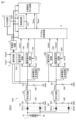
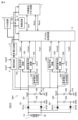
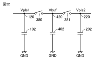
- 22 is a diagram for explaining an example of a method of supplying voltage to a power supply terminal of the voltage buffer of FIG. 21.
- FIG. 13 is a circuit block diagram of a battery-less multi-rotation encoder according to a fifth embodiment.
- 24 is a timing chart showing an example of normal processing of the battery-less multi-rotation encoder of FIG. 23.
- a batteryless multi-rotation encoder will be described as an example, but the technology of the present disclosure is not limited to this.
- the technology of the present disclosure can be applied to various semiconductor devices that operate with current pulses from a power generation element that generates power using electromagnetic induction. Note that in the following description, the same or corresponding parts will be given the same reference symbols, and their description may not be repeated.
- Fig. 1 is a circuit block diagram of a batteryless multi-rotation encoder ENC1 according to embodiment 1.
- the batteryless multi-rotation encoder ENC1 in Fig. 1 includes a power generating element 1 that generates power by utilizing electromagnetic induction, and a semiconductor device SD1 that operates by current pulses generated by this power generating element 1.
- the semiconductor device SD1 includes rectifier circuits 101, 201, storage capacitance elements 102, 202, voltage determination circuits 103, 203, charge amount determination circuits 104, 204, reference voltage generation circuits 105, 205, a selection circuit 2, a constant voltage circuit 3, a POR (Power On Reset) circuit 4, an oscillation circuit 5, a digital processing circuit 6, and a non-volatile memory 7.
- the voltage judgment circuit 103 and the charge judgment circuit 104 constitute a judgment circuit 130 that judges whether the amount of power generated by the power generating element 1 is sufficient.
- the voltage judgment circuit 203 and the charge judgment circuit 204 constitute a judgment circuit 230 that judges whether the amount of power generated by the power generating element 1 is sufficient.
- the power generating element 1 is connected to the rectifier circuit 101 and the rectifier circuit 201.
- the rectifier circuit 101 and the rectifier circuit 201 are connected to the power generating element 1 so that the rectification direction is opposite.
- the output of the rectifier circuit 101 is stored in the capacitance element 102, and the output of the rectifier circuit 201 is stored in the capacitance element 202. Therefore, depending on the polarity of the current pulse generated in the power generating element 1, charge is accumulated in one of the capacitance elements 102, 202, and a voltage is generated.
- the rectifier circuit 101 includes diodes 101A and 101B.
- a first end 1A of the coil serving as the power generating element 1 is connected to a high-potential node 120 of the capacitance element 102 via a forward diode 101A.
- a second end 1B of the coil serving as the power generating element 1 is connected to a low-potential node of the capacitance element 102, i.e., ground GND, via a reverse diode 101B.
- the rectifier circuit 201 includes diodes 201A and 201B.
- the first end 1A of the coil serving as the power generating element 1 is connected to the low-potential node of the capacitance element 202, i.e., ground GND, via the reverse diode 201B.
- the second end 1B of the coil serving as the power generating element 1 is connected to the high-potential node 220 of the capacitance element 202 via the forward diode 201A.
- the voltage Vpls1 of the high-potential side node 120 of the capacitive element 102 is input to the selection circuit 2, the voltage judgment circuit 103, the charge amount judgment circuit 104, and the reference voltage generation circuit 105.
- the voltage Vpls2 of the high-potential side node 220 of the capacitive element 202 is input to the selection circuit 2, the voltage judgment circuit 203, the charge amount judgment circuit 204, and the reference voltage generation circuit 205.
- the reference voltage generation circuit 105 generates a constant reference voltage Vref1 based on the voltage Vpls1 of the capacitive element 102, and does not depend on the magnitude of the voltage Vpls1.
- the generated reference voltage Vref1 is input to the voltage evaluation circuit 103 and the charge amount evaluation circuit 104.
- the reference voltage generation circuit 205 generates a constant reference voltage Vref2 based on the voltage Vpls2 of the capacitive element 202, and does not depend on the magnitude of the voltage Vpls2.
- the generated reference voltage Vref2 is input to the voltage evaluation circuit 203 and the charge amount evaluation circuit 204.
- the voltage evaluation circuit 103 determines whether or not a first judgment condition is satisfied, that is, the voltage Vpls1 of the capacitive element 102 exceeds a first judgment value. This determines whether or not the voltage level of the voltage Vpls1 of the capacitive element 102 is sufficient to start processing in the digital processing circuit 6.
- the voltage evaluation circuit 103 outputs the judgment result to the selection circuit 2 and the digital processing circuit 6 as a judgment signal Vdet1.
- the voltage evaluation circuit 203 determines whether or not a first judgment condition is satisfied, that is, the voltage Vpls2 of the capacitive element 202 exceeds a first judgment value.
- the voltage evaluation circuit 203 outputs the judgment result to the selection circuit 2 and the digital processing circuit 6 as a judgment signal Vdet2.
- the selection circuit 2 selects one of the voltages Vpls1 and Vpls2 that has reached a sufficient voltage level based on the judgment signals Vdet1 and Vdet2.
- the selection circuit 2 outputs the selected voltage Vpls1 or Vpls2 to the constant voltage circuit 3.
- the charge amount determination circuit 204 receives the voltage Vpls2 of the capacitive element 202 and the reference voltage Vref2 as well as the determination timing signal Vtm2 from the digital processing circuit 6. The charge amount determination circuit 204 determines whether the charge amount of the capacitive element 202 (proportional to the voltage Vpls2) exceeds a second determination value at the timing when the determination timing signal Vtm2 is activated. This determines whether the charge amount of the capacitive element 202 is sufficient for subsequent processing by the digital processing circuit 6.
- the charge amount determination circuit 204 determines that the charge amount of the capacitive element 202 is insufficient (i.e., the second determination condition is not satisfied), it outputs an interruption signal Vstop2 indicating an active state (for example, high level) to the digital processing circuit 6.
- the POR circuit 4 releases the reset signal RST when the power supply voltage Vdig output from the constant voltage circuit 3 reaches the minimum operating power supply voltage.
- the digital processing circuit 6 is composed of logic circuits.
- the digital processing circuit 6 outputs a write signal Write to the non-volatile memory 7 and receives an input of a read signal Read from the non-volatile memory 7.
- the current generated by power generating element 1 is selectively supplied to capacitive element 102 or capacitive element 202 through rectifier circuit 101 or rectifier circuit 201 depending on the direction of the current.
- the supplied current is stored as a charge in the capacitive element and converted into a voltage.
- the rectifier circuit 101 when a current is generated in the direction from the second end 1B to the first end 1A of the power generating element 1 in FIG. 1, the rectifier circuit 101 becomes conductive. In this case, the current generated in the power generating element 1 is supplied to the capacitance element 102. Conversely, when a current is generated in the direction from the first end 1A to the second end 1B of the power generating element 1, the rectifier circuit 201 becomes conductive. In this case, the current generated in the power generating element 1 is supplied to the capacitance element 202.
- VD VDa x VDb
- comparing the voltage Vpls1 with the determination voltage VD is equivalent to comparing Vpls1/VDa with VDb. Therefore, it is not necessary to use the voltage Vpls1 of the capacitive element 102 as the subject of comparison as is.
- the voltage Vpls2 of the capacitive element 202 is input to the reference voltage generation circuit 205, which generates the reference voltage Vref2.
- the voltage judgment circuit 203 generates a judgment voltage VD from the reference voltage Vref2 generated by the reference voltage generation circuit 205, and judges whether Vpls2 is higher or lower than the judgment voltage VD.
- the judgment result is output to the digital processing circuit 6 as a judgment signal Vdet2. If the voltage Vpls2 of the capacitive element 202 is higher than the judgment voltage VD, a high level is output as the judgment signal Vdet2, and if the voltage Vpls2 is lower than the judgment voltage VD, a low level is output as the judgment signal Vdet2.
- determination signals Vdet1 and Vdet2 may also be negative logic.
- the voltage Vpls1 of the capacitive element 102 exceeds the determination voltage VD, so the determination signal Vdet1 output from the voltage determination circuit 103 switches to a high level.
- the selection circuit 2 selectively supplies either the voltage Vpls1 or Vpls2 to the constant voltage circuit 3 based on the logical values of the judgment signals Vdet1 and Vdet2.
- the judgment signal Vdet1 is at a high level
- the voltage Vpls1 is selected
- the judgment signal Vdet2 is at a high level
- the voltage Vpls2 is selected. Since it is conceivable that both signals may be at a high level at the same time, the selection circuit 2 performs exclusive processing, such as preferentially selecting the judgment signal that first indicated an active state.
- the constant voltage circuit 3 When the voltage Vpls1 or Vpls2 is supplied to the constant voltage circuit 3, the constant voltage circuit 3 outputs the voltage Vdig.
- the voltage Vpls1 In the case of FIG. 2, the voltage Vpls1 is input to the constant voltage circuit 3 at time t1, causing the power supply voltage Vdig to rise.
- the voltage Vdig is supplied as a power supply voltage to the POR circuit 4, the oscillator circuit 5, the digital processing circuit 6, and the non-volatile memory circuit 7.
- the power supply voltage Vdig reaches the desired voltage, and the POR circuit 4 releases the reset signal RST.
- the reset signal RST switches from high to low. This enables the oscillator circuit 5, digital processing circuit 6, and non-volatile memory 7 to operate and start processing.
- the digital processing circuit 6 counts the number of current pulses each time a current pulse is generated in the power generating element 1, and determines the direction of the current pulse based on the judgment signals Vdet1 and Vdet2.
- the digital processing circuit 6 determines the rotation speed and direction of rotation of the object to be observed (hereinafter collectively referred to as the rotation state) based on this information.
- the digital processing circuit 6 then stores the determined rotation state in the non-volatile memory 7.
- the digital processing circuit 6 first reads (Reads) information on the previous rotation state from the non-volatile memory 7 between time t2 and time t3.
- the digital processing circuit 6 sends an active (high level) determination timing signal Vtm1 to the charge amount determination circuit 104.
- the charge amount determination circuit 104 determines whether the charge stored in the capacitive element 102 at this time is equal to or greater than the determination value. If the charge amount of the capacitive element 102 is equal to or greater than the determination value, the charge amount determination circuit 104 sets the interrupt signal Vstop1 to low level, and if the charge amount of the capacitive element 102 is less than the determination value, the interrupt signal Vstop1 to high level.
- the determination value of the charge amount determination circuit 104 is determined based on the amount of charge required for the write process of the non-volatile memory 7.
- the judgment value is determined based on the reference voltages Vref1 and Vref2.
- the digital processing circuit 6 may not send the judgment timing signal Vtm1 to the charge amount judgment circuit 104, and the charge amount judgment circuit 104 may constantly compare the charge amount of the capacitive element 102 with the judgment value and constantly transmit the result to the digital processing circuit 6. In this case, the digital processing circuit 6 uses the judgment result received at the timing when the update of the rotation state is completed (time t4).
- the digital processing circuit 6 determines that the charge required for subsequent processing has accumulated in the capacitive element 102. In this case, the digital processing circuit 6 writes the updated data (i.e., information on the rotation state) to the non-volatile memory 7 between the next time t4 and time t5, and ends the series of processes.
- the digital processing circuit 6 determines that the charge required for subsequent processing has not accumulated in the capacitive element 102. In this case, the digital processing circuit 6 executes the interrupt processing without writing the updated data to the non-volatile memory 7.
- the digital processing circuit 6 transmits the determination timing signal Vtm2 in the active state (high level) to the charge amount determination circuit 204.
- the charge amount determination circuit 204 determines whether the charge accumulated in the capacitive element 202 at this time is equal to or greater than the determination value. If the charge amount of the capacitive element 202 is equal to or greater than the determination value, the charge amount determination circuit 204 sets the interruption signal Vstop2 to low level, and if the charge amount of the capacitive element 202 is less than the determination value, the interruption signal Vstop2 to high level.
- the digital processing circuit 6 If the interruption signal Vstop2 is low level, the digital processing circuit 6 writes the updated data to the non-volatile memory 7 and ends the series of processes. On the other hand, if the interruption signal Vstop2 is high level, the digital processing circuit 6 executes interruption processing that does not write the updated data to the non-volatile memory 7.
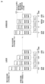
- FIG. 4 is a conceptual diagram showing the amount of charge stored in the capacitive elements 102 and 202 at the start and end of each read, update, and write process.
- the judgment voltage VD1 of the voltage judgment circuits 103 and 203 is determined by (the lower limit operating voltage of the constant voltage circuit) + (the charge required for all processing) x (the capacitance of the capacitive element), and cannot be lowered below that value.
- the lower limit of the charge amount at which all processes can be executed is when the above-mentioned determination voltage VD1 is equal to the peak value of the voltages Vpls1 and Vpls2 of the capacitive elements 102 and 202.
- the voltages Vpls1 and Vpls2 of the capacitive elements 102 and 202 gradually decrease, reaching the lower limit operating voltage VL of the constant voltage circuit 3 when all processes are completed.
- the judgment voltage VD2 of the voltage judgment circuits 103, 203 can be (the lower limit operating voltage of the constant voltage circuit) + (the charge required for reading and updating) x (the capacitance of the capacitive element).
- the judgment voltage of the voltage judgment circuits 103, 203 can be lowered by the voltage equivalent value VD3 of the charge required for the write process.
- the charge required for the write process must be supplied from the power generation element 1 between the start of the process and the start of the write process. Whether or not the charge required for the write process has been supplied to the capacitive element 102, 202 is judged by the charge amount judgment circuit 104, 204.
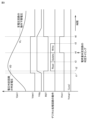
- FIG. 5 is a diagram conceptually showing the change over time of the voltage Vpls1 of the capacitive element 102.
- the voltage Vpls1 shown in FIG. 5 corresponds to a charge amount greater than the minimum charge amount shown in FIG. 4.
- an amount of charge sufficient to execute all processes is stored in the capacitive element 102 at the start time t202 of the processes.
- the peak value of the voltage Vpls1 of the capacitive element 102 is equal to or greater than the judgment voltage VD1 of the voltage judgment circuit 103.
- the judgment voltage VD2 of the voltage judgment circuit 103 can be made lower than the judgment voltage VD1 of the comparative example. Therefore, processing starts before the peak value, that is, at time t2 during power generation by the power generation element 1. As a result, the peak value of the generated voltage can be lowered, and the reverse current generated in the coil serving as the power generation element 1 can be suppressed.
- the batteryless multi-rotation encoder ENC1 of this embodiment in the middle of a series of processes, it is determined whether the charge in the capacitive elements 102, 202 is sufficient to execute the subsequent processes. This makes it possible to hasten the start of the series of processes and suppress the rise in voltage of the capacitive elements 102, 202. As a result, the voltage applied to the coil serving as the power generating element 1 can be suppressed, so that the reverse voltage generated in the coil can be suppressed and the effective generated charge can be increased. Therefore, even if the power generating capacity of the power generating element is relatively low, it is possible to prevent missed detection of the power generating pulse and determine the rotation state.
- the charge amount of the capacitive elements 102 and 202 is determined before the write process, but the charge amount may also be determined before the read process or update process. However, since charge generated after the charge amount is determined is not taken into account in the charge amount determination, it is desirable to determine the charge amount as late as possible. The charge amount may also be determined at multiple times.
- circuit configurations [Examples of circuit configurations] 1, the reference voltage generating circuits 105 and 205, the voltage determining circuits 103 and 203, the charge amount determining circuits 104 and 204, the selection circuit 2, the constant voltage circuit 3, and the POR circuit 4 will be described below.
- the circuit configurations shown below are merely examples, and are not limited to these. Any circuit configuration may be used as long as it has the above-mentioned functions.
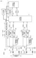
- Fig. 6 is a circuit diagram showing an example of the configuration of the reference voltage generating circuit 105 and the voltage evaluation circuit 103 in Fig. 1.
- the reference voltage generating circuit 205 and the voltage evaluation circuit 203 also have the same configuration.
- the reference voltage generating circuit 105 includes a plurality of diodes 301 connected in series, an NMOS (N-channel Metal-Oxide-Semiconductor) transistor 302, and resistor elements 303 to 305.
- NMOS N-channel Metal-Oxide-Semiconductor
- resistor elements 303 to 305 In the case of FIG. 6, three diodes 301A to 301C are provided as the plurality of diodes 301.
- NMOS transistor 302 The drain terminal of NMOS transistor 302 is connected to high potential node 120 of capacitance element 102.
- the source terminal of NMOS transistor 302 is connected to ground GND via resistor elements 303 and 304 connected in series.
- the gate terminal of NMOS transistor 302 is connected to high potential node 120 via resistor element 305, and is also connected to ground GND via diodes 301A to 301C connected in series in the forward direction.
- the source voltage of NMOS transistor 302 is a constant voltage determined according to the forward voltages of diodes 301A to 301C, regardless of the voltage Vpls1 of high-potential node 120.
- This constant source voltage is divided by resistor elements 303 and 304, and the divided voltage is output from connection node 309 of resistor elements 303 and 304 as reference voltage Vref1.
- the voltage evaluation circuit 103 includes a voltage comparator CMP1 and resistive elements 306 and 307.
- the resistive elements 306 and 307 are connected in series between the high-potential node 120 and ground GND.
- the non-inverting input terminal of the voltage comparator CMP1 is connected to a connection node 310 of the resistive elements 306 and 307.
- a reference voltage Vref1 is input to the inverting input terminal of the voltage comparator CMP1.
- the voltage comparator CMP1 compares the divided voltage obtained by dividing the voltage Vpls1 of the capacitive element 102 by the resistive elements 306 and 307 with the reference voltage Vref1. When the divided voltage of the voltage Vpls1 is greater than the reference voltage Vref1, the voltage comparator CMP1 activates the determination signal Vdet1.
- Fig. 7 is a circuit diagram showing an example of the configuration of the charge amount determination circuit 104 in Fig. 1. In Fig. 7, assuming that the charge amount of the capacitive element 102 is proportional to the voltage, the charge amount determination circuit 104 compares the voltage Vpls1 of the capacitive element 102 with a reference voltage 317. The charge amount determination circuit 204 has a similar configuration.
- the charge amount determination circuit 104 includes a voltage comparator CMP2, a D flip-flop 316, and a reference voltage 317.
- the inverting input terminal of the voltage comparator CMP2 is connected to the high potential side node 120 of the capacitive element 102.
- the reference voltage 317 is input to the non-inverting input terminal of the voltage comparator CMP2.
- the reference voltage 317 is generated, for example, from a reference voltage Vref1.
- the comparison result of the voltage comparator CMP2 is input to an input terminal D of the D flip-flop 316.
- An interrupt signal Vstop1 is output from an output terminal Q of the D flip-flop 316.
- a determination timing signal Vtm1 is input to a clock terminal CLK of the D flip-flop 316, and a determination signal Vdet1 is input to an inverting reset terminal RSTB of the D flip-flop 316.
- the D flip-flop 316 holds a logical value representing the comparison result of the voltage comparator CMP2 input to the input terminal D at the timing when the determination timing signal Vtm1 is activated to a high level.
- the D flip-flop 316 outputs the held logical value as an interruption signal Vstop1 from the output terminal Q. Therefore, when the reference voltage 317 is greater than the voltage Vpls1 of the capacitive element 102, a high-level interruption signal Vstop1 is output from the D flip-flop 316.
- the determination signal Vdet1 switches from a high level to a low level, the D flip-flop 316 is reset, and the interruption signal Vstop1 returns to a low level.
- FIG. 8 is a circuit diagram showing an example of the configuration of the selection circuit 2 in Fig. 1.
- the selection circuit 2 includes bidirectional switches 321 and 322, and NAND circuits 323 and 324 forming a flip-flop.
- the bidirectional switch 321 is configured by connecting two PMOS (P-channel Metal-Oxide-Semiconductor) transistors 321A and 321B in series with opposite polarity.
- the bidirectional switch 322 is configured by connecting two PMOS transistors 322A and 322B in series with opposite polarity.
- the output node 320 of the selection circuit 2 is connected to the high-potential side node 120 of the capacitance element 102 via the bidirectional switch 321, and is connected to the high-potential side node 220 of the capacitance element 202 via the bidirectional switch 322.
- the determination signal Vdet1 is input to a first input terminal of the NAND circuit 323.
- the determination signal Vdet2 is input to a first input terminal of the NAND circuit 324.
- the output terminal of the NAND circuit 323 is connected to a second input terminal of the NAND circuit 324 and is connected to the gate terminals of the PMOS transistors 321A and 321B that constitute the bidirectional switch 321.
- the output terminal of the NAND circuit 324 is connected to a second input terminal of the NAND circuit 323 and is connected to the gate terminals of the PMOS transistors 322A and 322B that constitute the bidirectional switch 322.
- the bidirectional switch 321 is in a conductive state and the bidirectional switch 322 is in a non-conductive state, so that the voltage Vpls1 of the capacitive element 102 is output from the output node 320 of the selection circuit 2.
- the output signal of the NAND circuit 323 becomes a high level and the output signal of the NAND circuit 324 becomes a low level.
- the bidirectional switch 321 becomes non-conductive and the bidirectional switch 322 becomes conductive, so that the voltage Vpls2 of the capacitive element 202 is output from the output node 320 of the selection circuit 2.
- Fig. 9 is a circuit diagram showing an example of the configuration of the constant voltage circuit 3 of Fig. 1.
- the constant voltage circuit 3 includes a PMOS transistor 331, resistance elements 332 and 333, a differential amplifier AMP1, and a reference voltage 334.
- the reference voltage 334 may be generated by utilizing reference voltages Vref1 and Vref2.
- the source terminal of the PMOS transistor 331 is connected to the output node 320 of the selection circuit 2.
- the drain terminal of the PMOS transistor 331 is connected to the output node 335 of the constant voltage circuit 3 and is connected to ground GND via the series-connected resistor elements 332 and 333.
- the non-inverting input terminal of the differential amplifier AMP1 is connected to the connection node 336 of the resistor elements 332 and 333.
- connection node 336 is equal to reference voltage 334, so that the power supply voltage Vdig output from output node 335 is a constant value that is not dependent on the magnitude of voltages Vpls1/Vpls2.
- FIG. 10 is a circuit diagram showing an example of the configuration of the POR circuit 4 of Fig. 1.
- the POR circuit 4 includes a low-pass filter 340 including a resistive element 341 and a capacitor 342, a voltage comparator CMP3, and a reference voltage 343.
- the reference voltage 343 may be generated by utilizing reference voltages Vref1 and Vref2.
- the power supply voltage Vdig output from the constant voltage circuit 3 is input to the inverting input terminal of the voltage comparator CMP3 via the low-pass filter 340.
- the reference voltage 343 is input to the non-inverting input terminal of the voltage comparator CMP3.
- Fig. 11 is a circuit block diagram of a batteryless multi-rotation encoder ENC2 according to embodiment 2.
- the semiconductor device SD2 of the batteryless multi-rotation encoder ENC2 in Fig. 11 differs from the semiconductor device SD1 of the batteryless multi-rotation encoder ENC1 in Fig. 1 in that it includes peak determination circuits 106, 206 instead of the charge amount determination circuits 104, 204.
- the voltage determination circuit 103 and the peak determination circuit 106 form a determination circuit 130
- the voltage determination circuit 203 and the peak determination circuit 206 form a determination circuit 230.
- the peak determination circuit 106 receives the voltage Vpls1 of the capacitive element 102 and the reference voltage Vref1 output from the reference voltage generation circuit 105. The peak determination circuit 106 determines whether or not a second determination condition is satisfied, that is, the peak value of the voltage Vpls1 of the capacitive element 102 has reached the determination voltage VP, and outputs a determination signal Vpeak1 representing the determination result to the digital processing circuit 6.
- the peak determination circuit 206 receives the voltage Vpls2 of the capacitive element 202 and the reference voltage Vref2 output from the reference voltage generation circuit 205. The peak determination circuit 206 determines whether or not a second determination condition is satisfied, that is, the peak value of the voltage Vpls2 of the capacitive element 202 reaches the determination voltage VP, and outputs a determination signal Vpeak2 representing the determination result to the digital processing circuit 6.
- FIG. 11 The rest of the configuration in FIG. 11 is the same as in FIG. 1, so the same or corresponding parts are given the same reference symbols and will not be described repeatedly.
- Fig. 12 is a timing chart showing an example of normal processing of the batteryless multi-rotation encoder ENC2 of Fig. 11.
- Fig. 13 is a timing chart showing an example of interruption processing of the batteryless multi-rotation encoder ENC2 of Fig. 11.
- the timing charts in Figures 12 and 13 correspond to the timing charts in Figures 2 and 3 of the first embodiment, and the operations other than peak determination by the peak determination circuits 106 and 206 are similar.
- the determination timing signals Vtm1 and Vtm2 used in the charge amount determination circuits 104 and 204 in the first embodiment are not necessary.
- the peak determination circuit 106 continuously monitors whether or not the peak value of the voltage Vpls1 of the capacitive element 102 has reached the determination voltage VP from the start of power generation by the power generating element 1. More specifically, if the peak value of the voltage Vpls1 of the capacitive element 102 exceeds the determination voltage VP even once, the peak determination circuit 106 maintains the determination signal Vpeak1 that it outputs in an active state (for example, high level), and if the peak value never exceeds the determination voltage VP, it maintains the determination signal Vpeak1 in an inactive state (for example, low level).
- the waveform of the voltage Vpls1 of the capacitive element 102 has an upwardly convex waveform that gradually rises during power generation, reaches a peak, and then gradually drops. Therefore, when the current voltage Vpls1 of the capacitive element 102 exceeds the judgment voltage VP at least temporarily, the peak judgment circuit 106 switches the judgment signal Vpeak1 from low level to high level, and then maintains the judgment signal Vpeak1 at high level.
- the peak determination circuit 206 operates in a similar manner. Specifically, when the peak value of the voltage Vpls2 of the capacitive element 202 exceeds the determination voltage VP at least temporarily, the peak determination circuit 206 maintains the determination signal Vpeak2 that it outputs in an active state (for example, a high level), and maintains the determination signal Vpeak2 in an inactive state (for example, a low level) if the peak value never exceeds the determination voltage VP.
- the digital processing circuit 6 monitors the judgment signals Vpeak1, Vpeak2 output from the peak judgment circuits 106, 206. If the judgment signals Vpeak1, Vpeak2 are at a high level, the digital processing circuit 6 starts the write process, and if they are at a low level, the digital processing circuit 6 does not execute the write process. It is desirable to determine whether the judgment signals Vpeak1, Vpeak2 are at a high level or not just before starting the write process. If the judgment is made at an earlier timing and the voltages Vpls1, Vpls2 of the capacitive elements 102, 202 reach their peaks after the judgment, there is the inconvenience that the charge generated by the power generating element 1 between the judgment and the time they reach their peaks is not taken into account.
- the voltage Vpls1 of the capacitive element 102 reaches the judgment voltage VP, so the peak judgment circuit 106 switches the judgment signal Vpeak1 from low level to high level.
- the judgment signal Vpeak1 is then maintained at a high level until the voltage Vpls1 of the capacitive element 102 drops to the lower limit voltage VL of the constant voltage circuit 3 at time t6.
- the digital processing circuit 6 After the update process is completed, at time t4 immediately before the start of the write process, the digital processing circuit 6 confirms that the determination signal Vpeak1 is at a high level and then starts the write process.
- the digital processing circuit 6 determines that the determination signal Vpeak1 is at a low level, it executes an interrupt process without starting the write process.
- FIG. 14 is a diagram illustrating an example of a mechanism for detecting write errors. Error detection bits are provided at the beginning and end of data written to non-volatile memory 7 during a write process. Digital processing circuit 6 writes "0" to the first and last bits of the write data when an even-numbered (2n) power generation pulse occurs. Digital processing circuit 6 writes "1" to the first and last bits of the write data when an odd-numbered (2n+1) power generation pulse occurs.
- the first and last bits of the read data when the 2n+1th power generation pulse occurs will be "0", and the first and last bits of the read data when the 2(n+1)th power generation pulse occurs will be "1".
- the write error detection mechanism described above may be incorporated into the digital processing circuit 6 of the semiconductor device SD1 of the first embodiment for safety purposes in case of unexpected charge consumption.
- Example of peak determination circuit configuration An example of the configuration of the peak determination circuits 106 and 206 in Fig. 11 will be described below.
- the circuit configuration shown below is merely an example, and is not limited to this. Any circuit configuration may be used as long as it has the above-mentioned functions.
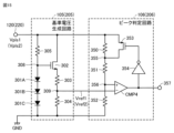
- FIG. 15 is a circuit diagram showing an example of the configuration of the peak determination circuit 106 in FIG. 11.
- the threshold of the voltage comparator has hysteresis.
- the peak determination circuit 206 has a similar configuration.
- the peak determination circuit 206 includes resistive elements 350, 351, and 352, a voltage comparator CMP4, a NOT circuit 354, and a PMOS transistor 353.
- the resistive elements 350, 351, and 352 are connected in series in this order between the high potential side node 120 of the capacitive element 102 and ground GND.
- the non-inverting input terminal of the voltage comparator CMP4 is connected to a connection node 356 between the resistive elements 351 and 352.
- a reference voltage Vref1 is input to the inverting input terminal of the voltage comparator CMP4.
- the PMOS transistor 353 is connected in parallel with the resistive element 350.
- the output terminal of the voltage comparator CMP4 is connected to an output node 357 of the peak determination circuit 106 and is connected to the gate terminal of the PMOS transistor 353 via the NOT circuit 354.
- the output of the voltage comparator CMP4 is at a low level and the PMOS transistor 353 is in an off state.
- the voltage comparator CMP4 compares the voltage Vpls1 with the first threshold value Vref1 x (r0 + r1 + r2)/r2.
- the voltage comparator CMP4 compares the voltage Vpls1 with the second threshold Vref1 ⁇ (r1+r2)/f2. Since the second threshold is smaller than the first threshold, the output of the voltage comparator CMP4 remains at a high level. A similar effect can be obtained by adding a latch circuit to the output of the voltage comparator CMP4.
- FIG. 16 is a circuit diagram showing another example of the configuration of the peak determination circuit 106 in FIG. 11.
- the peak determination circuit 106 in FIG. 16 detects the height of the peak of the voltage Vpls2 using a peak detection circuit, and compares the height of the detected peak with a reference voltage.
- the peak determination circuit 206 has a similar configuration.
- the peak determination circuit 106 includes a peak detection circuit 360, a voltage comparator CMP5, and a reference voltage 364.
- the peak detection circuit 360 includes a diode 361, an NMOS transistor 362, and a capacitor 363.
- the reference voltage 364 may be generated using the reference voltages Vref1 and Vref2.
- the anode of the diode 361 is connected to the high potential side node 120 of the capacitance element 102, and the cathode of the diode 361 is connected to ground GND via the capacitor 363.
- the voltage Vpls1 is held in the capacitor 363 until the voltage Vpls1 reaches its peak.
- a reset signal RST1 is input to the gate terminal of the NMOS transistor 362, resetting the voltage of the capacitor 363.
- the voltage comparator CMP5 compares the voltage of the capacitor 363 with the reference voltage 364, and sets the determination signal Vpeak1 to a high level when the voltage of the capacitor 363 exceeds the reference voltage 364.
- FIG. 17 is a circuit block diagram of a batteryless multi-rotation encoder ENC3 according to embodiment 3.
- the semiconductor device SD3 of the batteryless multi-rotation encoder ENC3 in Fig. 17 differs from the semiconductor device SD1 of the batteryless multi-rotation encoder ENC1 in Fig. 1 in the following points.
- a boost circuit 107 is provided between a connection node 121, which commonly connects the selection circuit 2, the voltage evaluation circuit 103, the charge amount evaluation circuit 104, and the reference voltage generation circuit 105, and a high-potential node 120 of the capacitance element 102.
- a boost circuit 207 is provided between a connection node 221, which commonly connects the selection circuit 2, the voltage evaluation circuit 203, the charge amount evaluation circuit 204, and the reference voltage generation circuit 205, and a high-potential node 220 of the capacitance element 202.
- another capacitance element 108 is connected between the connection node 121 and ground GND.
- another capacitance element 208 is connected between the connection node 221 and ground GND.
- the boost circuit 107 generates a voltage Vpls1 by boosting the voltage V1 of the capacitive element 102.
- the voltage Vpls1 is stored as an electric charge in the capacitive element 108.
- the constant voltage circuit 3 generates a power supply voltage Vdig from the voltage Vpls1 of the capacitive element 108.
- the boost circuit 207 generates a voltage Vpls2 by boosting the voltage V2 of the capacitive element 202.
- the voltage Vpls2 is stored as an electric charge in the capacitive element 208.
- the constant voltage circuit 3 generates a power supply voltage Vdig from the voltage Vpls2 of the capacitive element 208.
- the configuration of the boost circuits 107 and 207 is not particularly limited. For example, they may be configured to connect an isolated or non-isolated DC/DC converter via a buffer amplifier for converting current to voltage.
- FIG. 17 Other configurations in FIG. 17 are similar to those in FIG. 1, so the same or corresponding parts are given the same reference numerals and the description will not be repeated. Note that the boost circuits 107, 207 and the capacitive elements 108, 208 in FIG. 17 can also be combined with the semiconductor device SD2 of the batteryless multi-rotation encoder ENC2 of the second embodiment shown in FIG. 11.
- Fig. 18 is a timing chart showing an example of normal processing of the battery-less multi-rotation encoder ENC3 of Fig. 17.
- the timing chart of Fig. 18 differs from the timing chart of Fig. 2 in that the voltage Vpls1 obtained by boosting the voltage V1 of the capacitance element 102 is used to drive the constant voltage circuit 3, but other points of Fig. 18 are similar to those of Fig. 2.
- the same reference symbols are used for parts that are the same as or correspond to those of Fig. 2.
- the constant voltage circuit 3 starts operating. This causes the digital processing circuit 6 to execute the read process and update process.
- the charge amount determination circuit 104 determines whether the charge amount corresponding to the boosted voltage Vpls1 is equal to or greater than the determination value. As a result, if the charge amount corresponding to the boosted voltage Vpls1 is equal to or greater than the determination value, the digital processing circuit 6 executes the write process and completes the series of processes. On the other hand, if the charge amount corresponding to the boosted voltage Vpls1 is less than the determination value, as described with reference to FIG. 3, the digital processing circuit 6 executes the interrupt process without writing the updated data to the non-volatile memory 7.
- the capacitance of the capacitive elements 108, 208 on the output side of the boost circuits 107, 207 is reduced, the voltage applied to the power generating element 1 does not increase. Therefore, the capacitance of the capacitive elements 108, 208 can be reduced. This makes it possible to reduce the "unusable charge" described with reference to FIG. 4, that is, (capacitance of the capacitive element) x (lower limit operating voltage of the constant voltage circuit), and therefore makes it possible to use more charge.
- the boost circuits 107, 207 depending on the power conversion efficiency of the boost circuits 107, 207, a considerable amount of charge may be lost in the boost circuits 107, 207. Therefore, if the increase in the amount of usable charge due to the above effect is greater than the decrease in the charge in the boost circuits 107, 207, the charge generated in the power generating element 1 can be used more efficiently.
- Embodiment 4 is a circuit block diagram of a battery-less multi-rotation encoder ENC4 according to embodiment 4. In embodiment 4, an example of a simple boost circuit using a capacitance element is shown.
- the semiconductor device SD4 of the batteryless multi-rotation encoder ENC4 in FIG. 19 differs from the semiconductor device SD1 of the batteryless multi-rotation encoder ENC1 in FIG. 1 in that it further includes other capacitive elements 109, 209 and variable voltage devices 110, 210.
- One end of the capacitance element 109 is connected to the high-potential node 120 of the capacitance element 102, and the other end of the capacitance element 109 is connected to ground GND via the variable voltage device 110. That is, the series connection of the capacitance element 109 and the variable voltage device 110 is connected in parallel to the capacitance element 102.
- one end of the capacitance element 209 is connected to the high-potential node 220 of the capacitance element 202, and the other end of the capacitance element 209 is connected to ground GND via the variable voltage device 210. That is, the series connection of the capacitance element 209 and the variable voltage device 210 is connected in parallel to the capacitance element 202.
- variable voltage device 110 increases the output voltage when the boost signal Vup1 received from the digital processing circuit 6 becomes active (e.g., high level). Similarly, the variable voltage device 210 increases the output voltage when the boost signal Vup2 received from the digital processing circuit 6 becomes active (e.g., high level).
- FIG. 19 Other configurations in FIG. 19 are similar to those in FIG. 1, so the same or corresponding parts are given the same reference numerals and the description will not be repeated. Note that the capacitive elements 109, 209 and the variable voltage devices 110, 210 in FIG. 19 can also be combined with the semiconductor device SD2 of the batteryless multi-rotation encoder ENC2 of the second embodiment shown in FIG. 11.
- Fig. 20 is a timing chart showing an example of normal processing of the battery-less multi-rotation encoder ENC4 of Fig. 19.
- the timing chart of Fig. 20 corresponds to the timing chart of the first embodiment of Fig. 2, and therefore the same reference symbols as in Fig. 2 are used for corresponding parts.
- the path along which the current flows is selectively determined by the direction of the current pulse and the action of the rectifier circuits 101 and 201.
- the current flows in a direction that enables the rectifier circuit 101, charge is supplied to the capacitance elements 102 and 109, and the voltage Vpls1 of the high-potential node 120 rises.
- the output voltage of the variable voltage generator 110 is maintained at the GND level or a low voltage.
- the voltage determination circuit 103 switches the determination signal Vdet1 from low to high, as in the first embodiment. This causes the selection circuit 2 to supply the voltage Vpls1 to the constant voltage circuit 3, and the constant voltage circuit 3 generates the power supply voltage Vdig from the supplied voltage Vpls1.
- the digital processing circuit 6 starts a series of processes (read, update, write) in the same way as in the first embodiment.
- the digital processing circuit 6 switches the boost signal Vup1 from low to high at time t31, which is before time t4 when the determination timing signal Vtm1 sent to the charge amount determination circuit 104 is switched from low to high. This causes the output voltage of the variable voltage generator 110 to rise, and this increase in output voltage increases the voltage Vpls1 of the high potential side node 120, so that the amount of charge that can be processed by the digital processing circuit 6 can be increased.
- the digital processing circuit 6 switches the determination timing signal Vtm1 from low level to high level.
- the charge amount determination circuit 104 determines whether the charge amount corresponding to the voltage Vpls1 of the high potential side node 120 is equal to or greater than the determination value. As a result, if the charge amount corresponding to the voltage Vpls1 is equal to or greater than the determination value, the digital processing circuit 6 executes the write process and completes the series of processes. On the other hand, if the charge amount corresponding to the voltage Vpls1 is less than the determination value, as described with reference to FIG. 3, the digital processing circuit 6 executes the interrupt process without writing the updated data to the non-volatile memory 7.
- the increase in the output voltage of the variable voltage generator 110 is ⁇ V
- the capacitance of the capacitance element 102 is C102
- the capacitance of the capacitance element 109 is C109
- This increase ⁇ Vpls1 in the voltage of the high potential side node 120 means that the charge that the digital processing circuit 6 can use for processing has increased by ⁇ Vpls1 ⁇ (C102+C109).
- FIG. 21 is a circuit diagram showing an example of the configuration of the variable voltage device 110 in FIG. 19.
- FIG. 21 also shows the capacitive elements 102 and 109 in FIG. 19.
- the variable voltage device 210 has a similar configuration.
- the variable voltage device 110 includes an NMOS transistor 370, a voltage buffer 371, and resistor elements 372 and 373.
- the output terminal of the voltage buffer 371 is connected to the high potential side node 120 of the capacitor element 102 via the capacitor element 109.
- a voltage Vbuf different from the voltage Vpls1 of the capacitor element 102 is supplied to the power supply terminal of the voltage buffer 371.
- the input terminal of the voltage buffer 371 is connected to the high potential side node 120 via the resistor element 372 and is connected to ground GND via the resistor element 373.
- an NMOS transistor 370 is connected in parallel with the resistor element 373.
- An inverted signal (/Vup1) of the boost signal Vup1 is input to the gate terminal of the NMOS transistor 370.
- the digital processing circuit 6 executes a series of processes using the charge stored in the capacitance element 102, it moves the remaining charge remaining from the processes to the capacitance element 402 by turning on the corresponding switch 380 for a certain period after the series of processes are completed.
- the digital processing circuit 6 executes a series of processes using the charge stored in the capacitance element 202, it moves the remaining charge remaining from the processes to the capacitance element 402 by turning on the corresponding switch 381 for a certain period after the series of processes are completed.
- the initial state no charge exists in the capacitance element 402, but if continuous operation is performed, the charge can be held in the capacitance element 402.
- the remaining charge can be reused by using the voltage Vbuf generated in the capacitance element 402 as the power supply voltage for the voltage buffer 371.
- variable voltage device 110 when the boost signal Vup1 is at a low level, the NMOS transistor 370 is turned on, which causes the input terminal of the voltage buffer 371 to be at ground potential and the low-potential node of the capacitance element 109 to be at ground level. In this case, the charge generated by the power generation element 1 is stored in the capacitance elements 102 and 109.
- Embodiment 5 is a circuit block diagram of a battery-less multi-rotation encoder ENC5 according to embodiment 5.
- Embodiment 5 is a modification of embodiment 4, and is characterized in that the variable voltage devices 110 and 210 are configured to switch the output voltage after the power generation element 1 finishes generating electricity.
- the current determination circuit 111 determines whether or not there is a current flowing between the high-potential side node 120 of the capacitance element 102 and the high-potential side node 122 of the capacitance element 109. After this current becomes zero, the current determination circuit 111 outputs a control signal to the variable voltage generator 110 so as to increase the output voltage of the variable voltage generator 110.
- the current determination circuit 111 includes a resistive element 111A and a voltage comparator 111B.
- the resistive element 111A is connected between a high potential side node 120 of the capacitive element 102 and a high potential side node 122 of the capacitive element 109.
- the voltage comparator 111B compares the voltages generated across the resistive element 111A to determine whether the voltage generated across the resistive element 111A is zero. Note that the configuration of the current determination circuit 111 is not limited to this configuration.
- the current determination circuit 211 determines whether or not there is a current flowing between the high-potential side node 220 of the capacitance element 202 and the high-potential side node 222 of the capacitance element 209. After this current becomes zero, the current determination circuit 211 outputs a control signal to the variable voltage generator 210 so as to increase the output voltage of the variable voltage generator 210.
- the current determination circuit 211 includes a resistive element 211A and a voltage comparator 211B.
- the resistive element 211A is connected between the high potential side node 220 of the capacitive element 202 and the high potential side node 222 of the capacitive element 209.
- the voltage comparator 211B compares the voltages generated across the resistive element 211A to determine whether the voltage generated across the resistive element 211A is zero. Note that the configuration of the current determination circuit 211 is not limited to this configuration.
- FIG. 23 Other configurations in FIG. 23 are similar to those in FIG. 1, so the same or corresponding parts are given the same reference numerals and the description will not be repeated. Note that the capacitive elements 109, 209, variable voltage devices 110, 210, and current determination circuits 111, 211 in FIG. 23 can also be combined with the semiconductor device SD2 of the batteryless multi-rotation encoder ENC2 of the second embodiment shown in FIG. 11.
- FIG. 24 is a timing chart showing an example of normal processing of the battery-less multi-rotation encoder ENC5 of FIG.
- the timing chart in FIG. 24 corresponds to the timing chart in FIG. 20 of the fourth embodiment, but differs from the timing chart in FIG. 20 in that an output signal indicating the judgment result of the current judgment circuit 111 is used instead of the boost signal Vup1 output from the digital processing circuit 6. Since the other points in FIG. 24 are the same as those in FIG. 20, the same reference characters are used for the same or corresponding parts and the description will not be repeated.
- variable voltage devices 110 and 210 are boosted while the power generating element 1 is generating power, the voltage applied to the power generating element 1 will rise, causing a reverse current to impede power generation. To prevent this, in embodiment 5, the variable voltage devices 110 and 210 are boosted after the power generating element 1 has finished generating power.
- the current determination circuit 111 determines the end of power generation by the power generating element 1 by detecting that the current flowing from the high potential side node 120 of the capacitance element 102 to the high potential side node 122 of the capacitance element 109 has become zero.
- the current determination circuit 111 outputs a high-level signal when it detects a current flowing in the direction from the high-potential side node 120 of the capacitance element 102 to the high-potential side node 122 of the capacitance element 109.
- the current determination circuit 111 outputs a low-level signal when the current becomes zero.
- the variable voltage device 110 increases the output voltage at time t31 when the output of the current determination circuit 111 switches from high to low.
- the output voltages of the variable voltage generators 110, 210 increase after the power generation of the power generation element 1 ends. Therefore, it is possible to suppress an increase in the reverse current of the power generation element 1 caused by an increase in the voltage of the high-potential side nodes 120, 220, and to increase the amount of effective charge that can be used for processing in the digital processing circuit 6, as in the fourth embodiment.
Landscapes
- Physics & Mathematics (AREA)
- Engineering & Computer Science (AREA)
- General Physics & Mathematics (AREA)
- Electromagnetism (AREA)
- Radar, Positioning & Navigation (AREA)
- Automation & Control Theory (AREA)
- Transmission And Conversion Of Sensor Element Output (AREA)
- Analogue/Digital Conversion (AREA)
- Measurement Of Current Or Voltage (AREA)
Priority Applications (3)
| Application Number | Priority Date | Filing Date | Title |
|---|---|---|---|
| JP2025513760A JPWO2024214291A1 (https=) | 2023-04-14 | 2023-04-14 | |
| CN202380096962.9A CN121002461A (zh) | 2023-04-14 | 2023-04-14 | 半导体装置及无电池多圈编码器 |
| PCT/JP2023/015201 WO2024214291A1 (ja) | 2023-04-14 | 2023-04-14 | 半導体装置およびバッテリレス多回転エンコーダ |
Applications Claiming Priority (1)
| Application Number | Priority Date | Filing Date | Title |
|---|---|---|---|
| PCT/JP2023/015201 WO2024214291A1 (ja) | 2023-04-14 | 2023-04-14 | 半導体装置およびバッテリレス多回転エンコーダ |
Publications (1)
| Publication Number | Publication Date |
|---|---|
| WO2024214291A1 true WO2024214291A1 (ja) | 2024-10-17 |
Family
ID=93059233
Family Applications (1)
| Application Number | Title | Priority Date | Filing Date |
|---|---|---|---|
| PCT/JP2023/015201 Ceased WO2024214291A1 (ja) | 2023-04-14 | 2023-04-14 | 半導体装置およびバッテリレス多回転エンコーダ |
Country Status (3)
| Country | Link |
|---|---|
| JP (1) | JPWO2024214291A1 (https=) |
| CN (1) | CN121002461A (https=) |
| WO (1) | WO2024214291A1 (https=) |
Citations (6)
| Publication number | Priority date | Publication date | Assignee | Title |
|---|---|---|---|---|
| JP2002318783A (ja) * | 2001-04-23 | 2002-10-31 | Denso Corp | マルチプロトコル型シリアル通信装置及びマイクロコンピュータ |
| JP2011185711A (ja) * | 2010-03-08 | 2011-09-22 | Mitsubishi Electric Corp | 多回転検出装置 |
| JP5769879B2 (ja) * | 2012-04-17 | 2015-08-26 | 三菱電機株式会社 | 多回転エンコーダ |
| JP2017022508A (ja) * | 2015-07-09 | 2017-01-26 | ローム株式会社 | 環境発電システム |
| JP2018156713A (ja) * | 2017-03-21 | 2018-10-04 | ルネサスエレクトロニクス株式会社 | 記憶装置及び記憶方法 |
| JP2022160170A (ja) * | 2021-04-06 | 2022-10-19 | エイブリック株式会社 | シミュレーション装置、シミュレーション方法、シミュレーションシステム及びプログラム |
-
2023
- 2023-04-14 JP JP2025513760A patent/JPWO2024214291A1/ja active Pending
- 2023-04-14 CN CN202380096962.9A patent/CN121002461A/zh active Pending
- 2023-04-14 WO PCT/JP2023/015201 patent/WO2024214291A1/ja not_active Ceased
Patent Citations (6)
| Publication number | Priority date | Publication date | Assignee | Title |
|---|---|---|---|---|
| JP2002318783A (ja) * | 2001-04-23 | 2002-10-31 | Denso Corp | マルチプロトコル型シリアル通信装置及びマイクロコンピュータ |
| JP2011185711A (ja) * | 2010-03-08 | 2011-09-22 | Mitsubishi Electric Corp | 多回転検出装置 |
| JP5769879B2 (ja) * | 2012-04-17 | 2015-08-26 | 三菱電機株式会社 | 多回転エンコーダ |
| JP2017022508A (ja) * | 2015-07-09 | 2017-01-26 | ローム株式会社 | 環境発電システム |
| JP2018156713A (ja) * | 2017-03-21 | 2018-10-04 | ルネサスエレクトロニクス株式会社 | 記憶装置及び記憶方法 |
| JP2022160170A (ja) * | 2021-04-06 | 2022-10-19 | エイブリック株式会社 | シミュレーション装置、シミュレーション方法、シミュレーションシステム及びプログラム |
Also Published As
| Publication number | Publication date |
|---|---|
| JPWO2024214291A1 (https=) | 2024-10-17 |
| CN121002461A (zh) | 2025-11-21 |
Similar Documents
| Publication | Publication Date | Title |
|---|---|---|
| JP6323558B2 (ja) | エンコーダ装置、駆動装置、ステージ装置、及びロボット装置 | |
| JP5287191B2 (ja) | ヒステリシススイッチングレギュレータ及びその動作制御方法 | |
| JP5806481B2 (ja) | 制御回路、電子機器及び電源の制御方法 | |
| CN101237237B (zh) | 使用滞后特性的单斜率模数转换器及模数转换方法 | |
| JP5109795B2 (ja) | 電圧検出回路およびスイッチング電源装置 | |
| US7684215B2 (en) | Switching mode power supply and driving method thereof | |
| JP2007020247A (ja) | 電源回路 | |
| JP4069866B2 (ja) | 交流信号のレベル検出回路 | |
| JP2003203488A (ja) | 不揮発性半導体メモリ | |
| JP2003143846A (ja) | 電源装置及びその制御方法 | |
| JP7800178B2 (ja) | スイッチング制御回路、電源回路 | |
| US6703848B2 (en) | Digitally controlled adaptive driver for sensing capacitive load | |
| WO2024214291A1 (ja) | 半導体装置およびバッテリレス多回転エンコーダ | |
| JP2002142448A (ja) | 昇圧回路 | |
| US20230396167A1 (en) | Control circuitry for controlling a power supply | |
| CN112639703B (zh) | 超声波感测电路及其驱动方法、探测基板和触控面板 | |
| JPH07264071A (ja) | A/d変換器 | |
| JP7577980B2 (ja) | 電流検出回路、電源回路 | |
| US7659787B2 (en) | Circuit for generating clock of semiconductor memory apparatus | |
| JP6154113B2 (ja) | 電子回路およびそれを備える電子機器 | |
| WO1999026290A1 (en) | Semiconductor integrated circuit, operating status detector, and electronic equipment | |
| WO2022097199A1 (ja) | 半導体装置及び多回転エンコーダ | |
| JP5190014B2 (ja) | 積分型ad変換回路およびad変換方法 | |
| JP5634233B2 (ja) | 絶縁型スイッチング電源 | |
| JP7459413B1 (ja) | エンコーダ及びモータ |
Legal Events
| Date | Code | Title | Description |
|---|---|---|---|
| 121 | Ep: the epo has been informed by wipo that ep was designated in this application |
Ref document number: 23933067 Country of ref document: EP Kind code of ref document: A1 |
|
| ENP | Entry into the national phase |
Ref document number: 2025513760 Country of ref document: JP Kind code of ref document: A |
|
| WWE | Wipo information: entry into national phase |
Ref document number: 2025513760 Country of ref document: JP |
|
| NENP | Non-entry into the national phase |
Ref country code: DE |
|
| 122 | Ep: pct application non-entry in european phase |
Ref document number: 23933067 Country of ref document: EP Kind code of ref document: A1 |