WO2024204006A1 - プリント配線板 - Google Patents
プリント配線板 Download PDFInfo
- Publication number
- WO2024204006A1 WO2024204006A1 PCT/JP2024/011580 JP2024011580W WO2024204006A1 WO 2024204006 A1 WO2024204006 A1 WO 2024204006A1 JP 2024011580 W JP2024011580 W JP 2024011580W WO 2024204006 A1 WO2024204006 A1 WO 2024204006A1
- Authority
- WO
- WIPO (PCT)
- Prior art keywords
- layer
- dielectric
- printed wiring
- dielectric layer
- wiring board
- Prior art date
- Legal status (The legal status is an assumption and is not a legal conclusion. Google has not performed a legal analysis and makes no representation as to the accuracy of the status listed.)
- Ceased
Links
Images


Classifications
-
- H—ELECTRICITY
- H05—ELECTRIC TECHNIQUES NOT OTHERWISE PROVIDED FOR
- H05K—PRINTED CIRCUITS; CASINGS OR CONSTRUCTIONAL DETAILS OF ELECTRIC APPARATUS; MANUFACTURE OF ASSEMBLAGES OF ELECTRICAL COMPONENTS
- H05K1/00—Printed circuits
- H05K1/02—Details
- H05K1/0213—Electrical arrangements not otherwise provided for
- H05K1/0237—High frequency adaptations
- H05K1/024—Dielectric details, e.g. changing the dielectric material around a transmission line
-
- H—ELECTRICITY
- H05—ELECTRIC TECHNIQUES NOT OTHERWISE PROVIDED FOR
- H05K—PRINTED CIRCUITS; CASINGS OR CONSTRUCTIONAL DETAILS OF ELECTRIC APPARATUS; MANUFACTURE OF ASSEMBLAGES OF ELECTRICAL COMPONENTS
- H05K1/00—Printed circuits
- H05K1/02—Details
- H05K1/03—Use of materials for the substrate
-
- H—ELECTRICITY
- H05—ELECTRIC TECHNIQUES NOT OTHERWISE PROVIDED FOR
- H05K—PRINTED CIRCUITS; CASINGS OR CONSTRUCTIONAL DETAILS OF ELECTRIC APPARATUS; MANUFACTURE OF ASSEMBLAGES OF ELECTRICAL COMPONENTS
- H05K1/00—Printed circuits
- H05K1/02—Details
- H05K1/03—Use of materials for the substrate
- H05K1/0313—Organic insulating material
- H05K1/0353—Organic insulating material consisting of two or more materials, e.g. two or more polymers, polymer + filler, + reinforcement
- H05K1/036—Multilayers with layers of different types
-
- H—ELECTRICITY
- H05—ELECTRIC TECHNIQUES NOT OTHERWISE PROVIDED FOR
- H05K—PRINTED CIRCUITS; CASINGS OR CONSTRUCTIONAL DETAILS OF ELECTRIC APPARATUS; MANUFACTURE OF ASSEMBLAGES OF ELECTRICAL COMPONENTS
- H05K3/00—Apparatus or processes for manufacturing printed circuits
- H05K3/46—Manufacturing multilayer circuits
- H05K3/4688—Composite multilayer circuits, i.e. comprising insulating layers having different properties
-
- H—ELECTRICITY
- H05—ELECTRIC TECHNIQUES NOT OTHERWISE PROVIDED FOR
- H05K—PRINTED CIRCUITS; CASINGS OR CONSTRUCTIONAL DETAILS OF ELECTRIC APPARATUS; MANUFACTURE OF ASSEMBLAGES OF ELECTRICAL COMPONENTS
- H05K2201/00—Indexing scheme relating to printed circuits covered by H05K1/00
- H05K2201/01—Dielectrics
- H05K2201/0137—Materials
- H05K2201/015—Fluoropolymer, e.g. polytetrafluoroethylene [PTFE]
-
- H—ELECTRICITY
- H05—ELECTRIC TECHNIQUES NOT OTHERWISE PROVIDED FOR
- H05K—PRINTED CIRCUITS; CASINGS OR CONSTRUCTIONAL DETAILS OF ELECTRIC APPARATUS; MANUFACTURE OF ASSEMBLAGES OF ELECTRICAL COMPONENTS
- H05K2201/00—Indexing scheme relating to printed circuits covered by H05K1/00
- H05K2201/01—Dielectrics
- H05K2201/0183—Dielectric layers
- H05K2201/0195—Dielectric or adhesive layers comprising a plurality of layers, e.g. in a multilayer structure
Definitions
- Patent Document 1 Japanese Patent Laid-Open Publication No. 2021-139779
- Patent Document 1 describes a printed wiring board.
- the printed wiring board described in Patent Document 1 has an internal layer, a first dielectric layer, and a second dielectric layer.
- the internal layer has a first main surface and a second main surface that is the opposite surface to the first main surface.
- the first dielectric layer and the second dielectric layer are disposed on the first main surface and the second main surface, respectively.
- the printed wiring board of the present disclosure comprises a substrate having a first main surface and a second main surface that is the opposite surface of the first main surface, and a first dielectric layer having a first adhesive layer disposed on the first main surface and a first fluororesin layer disposed on the first adhesive layer.
- FIG. 1 is a cross-sectional view of a printed wiring board 100 .
- 2A to 2C are diagrams showing the manufacturing process of the printed wiring board 100.
- FIG. 3 is a cross-sectional view illustrating the dielectric layer attachment step S2.
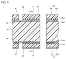
- FIG. 4 is a cross-sectional view illustrating the hole making step S3.
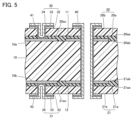
- FIG. 5 is a cross-sectional view illustrating the wiring forming step S4.
- the constituent material of the first dielectric layer and the constituent material of the second dielectric layer are a hydrocarbon-based resin material (polyphenylene ether resin). Therefore, in the printed wiring board described in Patent Document 1, the relative dielectric constant and the dielectric loss tangent of the first dielectric layer and the second dielectric layer are high, and there is room for improvement in the high-frequency characteristics when a high-frequency signal flows through the wiring arranged on the first dielectric layer and the second dielectric layer.
- the first and second dielectric layers are made of fluororesin, the dielectric constant and dielectric tangent of the first and second dielectric layers are reduced, but the first and second dielectric layers must be heated to high temperatures when they are bonded to the inner layer, which may damage the inner layer.
- This disclosure has been made in consideration of the problems with the conventional technology described above. More specifically, this disclosure provides a printed wiring board that can suppress damage to the substrate caused by the compression bonding of the dielectric layer and can improve high-frequency characteristics.
- the printed wiring board according to the embodiment includes a substrate having a first main surface and a second main surface opposite the first main surface, and a first dielectric layer having a first adhesive layer disposed on the first main surface and a first fluororesin layer disposed on the first adhesive layer.
- the printed wiring board of (1) above can suppress damage to the substrate caused by pressure bonding of the dielectric layer, and can improve high frequency characteristics.
- the thermal expansion coefficient of the first dielectric layer in the normal direction of the first main surface may be 400 ppm/K or less.
- the thermal expansion coefficient of the first adhesive layer in the normal direction of the first main surface may be 400 ppm/K or less.
- the thermal expansion coefficient of the first fluororesin layer may be 400 ppm or less in the normal direction of the first main surface.
- the first dielectric layer may have a relative dielectric constant of 3.4 or less.
- the printed wiring board of (5) above allows for further improvement in high frequency characteristics.
- the difference between the relative dielectric constant of the first fluororesin layer and the relative dielectric constant of the first adhesive layer may be 0.1 or less.
- the printed wiring board of (6) above allows for further improvement in high frequency characteristics.
- the dielectric tangent value of the first dielectric layer may be 0.003 or less.
- the printed wiring board of (7) above allows for further improvement in high frequency characteristics.
- the printed wiring boards of (1) to (7) above may further include a first wiring disposed on the substrate.
- the first adhesive layer may be disposed on the first main surface so as to cover the first wiring.
- the first adhesive layer may have a first surface facing the first fluororesin layer and a second surface opposite the first surface.
- the first surface may be flat.
- the second surface may have a recess in the area covering the first wiring.
- the first thickness which is the thickness of the first adhesive layer between the first wiring and the first fluororesin layer, may be 5 ⁇ m or more and 150 ⁇ m or less.
- the value obtained by dividing the first thickness by the sum of the first thickness and the second thickness, which is the thickness of the first fluororesin layer may be 0.02 or more and 0.75 or less. According to the printed wiring board of (11) above, it is possible to improve the high-frequency characteristics while improving the adhesion between the dielectric layer and the substrate.
- the peel strength between the first dielectric layer and the substrate may be 2.0 N/cm or more. With the printed wiring board of (12) above, it is possible to improve the adhesion between the dielectric layer and the substrate.
- the first adhesive layer and the first dielectric layer may contain a filler.
- the printed wiring boards of (1) to (13) above may further include a second dielectric layer having a second adhesive layer disposed on the second main surface and a second fluororesin layer disposed on the second adhesive layer.
- a printed wiring board according to the embodiment is referred to as a printed wiring board 100.
- FIG. 1 is a cross-sectional view of a printed wiring board 100.
- the printed wiring board 100 has a substrate 10, a wiring 11, a wiring 12, a dielectric layer 20, a dielectric layer 21, a wiring 30, and a wiring 31.
- the material of the substrate 10 is, for example, glass epoxy.
- the substrate 10 has a main surface 10a and a main surface 10b.
- the main surface 10a and the main surface 10b are end surfaces in the thickness direction of the substrate 10.
- the main surface 10b is the opposite surface to the main surface 10a.
- Wiring 11 and wiring 12 are arranged on main surface 10a and main surface 10b, respectively.
- the constituent material of wiring 11 and wiring 12 is, for example, copper. Although not shown, wiring may also be arranged inside substrate 10.
- the dielectric layer 20 is disposed on the main surface 10a so as to cover the wiring 11.
- the dielectric layer 20 has an adhesive layer 20a and a fluororesin layer 20b.
- the adhesive layer 20a is disposed on the main surface 10a so as to cover the wiring 11.
- the fluororesin layer 20b is disposed on the adhesive layer 20a.
- the adhesive layer 20a is a layer made of an adhesive.
- the adhesive constituting the adhesive layer 20a may be capable of being pressed onto the substrate 10 at a temperature of 200°C or less.
- the fluororesin layer 20b is a layer made of a fluororesin.
- the dielectric constant of the dielectric layer 20 may be 3.4 or less.
- the dielectric constant of the dielectric layer 20 is measured by the split cylinder method or the phase difference method.
- the dielectric tangent value of the dielectric layer 20 may be 0.003 or less.
- the dielectric tangent value of the dielectric layer 20 is measured by the split cylinder method or the phase difference method.
- the dielectric layer 20 is removed from the printed wiring board 100 by polishing or the like and then measured.
- a circuit pattern is formed on the surface of the dielectric layer 20 and then measured.
- the difference between the relative dielectric constant of the fluororesin layer 20b and the relative dielectric constant of the adhesive layer 20a may be 0.1 or less.
- the relative dielectric constant of the adhesive layer 20a (fluororesin layer 20b) can be calculated based on the relative dielectric constant of the dielectric layer 20 and the value of the dielectric tangent of the fluororesin layer 20b (adhesive layer 20a).
- the value of the dielectric tangent of the adhesive layer 20a and the value of the dielectric tangent of the fluororesin layer 20b may be 0.004 or less and 0.003 or less, respectively.
- the value of the dielectric tangent of the adhesive layer 20a can be calculated based on the value of the dielectric tangent of the dielectric layer 20 and the value of the dielectric tangent of the fluororesin layer 20b (adhesive layer 20a).
- the thermal expansion coefficient of the dielectric layer 20 in the normal direction to the main surface 10a may be 400 ppm/K or less.
- the thermal expansion coefficient of the dielectric layer 20 in the direction perpendicular to the normal direction to the main surface 10a may be 400 ppm/K or less.
- the thermal expansion coefficient of the dielectric layer 20 is measured by TMA (Thermo Mechanical Analysis). When the measurement object is a laminate, the measurement is performed on the dielectric layer 20 after only the dielectric layer 20 is removed by polishing or the like.
- the thermal expansion coefficient of the adhesive layer 20a in the normal direction to the main surface 10a and the thermal expansion coefficient of the fluororesin layer 20b in the normal direction to the main surface 10a may be 400 ppm/K or less.
- the thermal expansion coefficient of the adhesive layer 20a in a direction perpendicular to the normal direction of the main surface 10a and the thermal expansion coefficient of the fluororesin layer 20b in a direction perpendicular to the normal direction of the main surface 10a may be 400 ppm/K or less.
- the thermal expansion coefficient of the adhesive layer 20a (fluororesin layer 20b) can be calculated based on the thermal expansion coefficient of the dielectric layer 20 and the thermal expansion coefficient of the fluororesin layer 20b (adhesive layer 20a).
- the Young's modulus of the dielectric layer 20 may be 8 GPa or less.
- the Young's modulus of the adhesive layer 20a and the fluororesin layer 20b may be 8 GPa or less, respectively.
- the Young's modulus of the dielectric layer 20 (adhesive layer 20a, fluororesin layer 20b) is measured by a tensile test in accordance with JIS K 7127:1999. If the dimensions of the measurement object are less than 10 mm x 150 mm, the width, length, and distance between chucks are appropriately changed according to the dimensions before measurement. If the measurement object is a laminate, the dielectric layer 20 is removed by polishing or the like, and then the measurement is performed on the dielectric layer 20.
- the adhesive layer 20a and the fluororesin layer 20b may contain a filler.
- the constituent material of the filler is, for example, silica, titanium oxide, etc.
- the relative dielectric constant, dielectric tangent value, thermal expansion coefficient, and Young's modulus of the dielectric layer 20 (adhesive layer 20a, fluororesin layer 20b) can be adjusted by adjusting the filler content.
- the adhesive layer 20a has a first surface 20aa and a second surface 20ab.
- the first surface 20aa is the surface facing the fluororesin layer 20b
- the second surface 20ab is the surface opposite the first surface 20aa.
- the first surface 20aa is flat, and the second surface 20ab has a recess 20ac in the area covering the wiring 11.
- the peel strength between the dielectric layer 20 and the substrate 10 may be 2.0 N/cm or more.
- the peel strength between the dielectric layer 20 and the substrate 10 is measured as the adhesive strength at the interface to be measured after cutting out a sample in accordance with JIS C 5016. If the adhesive strength at the interface between the dielectric layer 20 and the substrate 10 (the interface between the adhesive layer 20a and the main surface 10a) is strong and peeling occurs at a location other than the interface, the adhesive strength at the interface is deemed to be equal to or greater than the result obtained by the test.
- the thickness of the adhesive layer 20a between the wiring 11 and the fluororesin layer 20b is defined as thickness T1
- the thickness of the fluororesin layer 20b is defined as thickness T2.
- Thickness T1 may be 5 ⁇ m or more and 150 ⁇ m or less.
- the value obtained by dividing thickness T1 by the sum of thickness T1 and thickness T2 may be 0.02 or more and 0.75 or less.
- Thickness T1 and thickness T2 are measured by length measurement during cross-sectional observation using a microscope or SEM (Scanning Electron Microscope).
- the dielectric layer 21 is disposed on the main surface 10b so as to cover the wiring 12.
- the dielectric layer 21 has an adhesive layer 21a and a fluororesin layer 21b.
- the adhesive layer 21a is disposed on the main surface 10b so as to cover the wiring 12.
- the fluororesin layer 21b is disposed on the adhesive layer 21a.
- the adhesive layer 21a is a layer made of an adhesive.
- the adhesive constituting the adhesive layer 21a may be capable of being pressed onto the substrate 10 at a temperature of 200°C or less.
- the fluororesin layer 21b is a layer made of a fluororesin.
- the dielectric constant of the dielectric layer 21 may be 3.4 or less.
- the dielectric constant of the dielectric layer 21 is measured in the same manner as the dielectric constant of the dielectric layer 20.
- the dielectric tangent value of the dielectric layer 21 may be 0.003 or less.
- the dielectric tangent value of the dielectric layer 21 is measured in the same manner as the dielectric tangent value of the dielectric layer 20.
- the difference between the relative dielectric constant of the fluororesin layer 21b and the relative dielectric constant of the adhesive layer 21a may be 0.1 or less.
- the relative dielectric constant of the adhesive layer 21a (fluororesin layer 21b) can be calculated based on the relative dielectric constant of the dielectric layer 21 and the value of the dielectric tangent of the fluororesin layer 21b (adhesive layer 21a).
- the values of the dielectric tangent of the adhesive layer 21a and the dielectric tangent of the fluororesin layer 21b may be 0.004 or less and 0.003 or less, respectively.
- the value of the dielectric tangent of the adhesive layer 21a can be calculated based on the value of the dielectric tangent of the dielectric layer 21 and the value of the dielectric tangent of the fluororesin layer 21b (adhesive layer 21a).
- the thermal expansion coefficient of the dielectric layer 21 in the normal direction of the main surface 10b may be 400 ppm/K or less.
- the thermal expansion coefficient of the dielectric layer 21 in the direction perpendicular to the normal direction of the main surface 10b may be 400 ppm/K or less.
- the thermal expansion coefficient of the dielectric layer 21 is measured by a method similar to that of the dielectric layer 20.
- the thermal expansion coefficient of the adhesive layer 21a in the normal direction of the main surface 10b and the thermal expansion coefficient of the fluororesin layer 21b in the normal direction of the main surface 10b may be 400 ppm/K or less.
- the thermal expansion coefficient of the adhesive layer 21a in the direction perpendicular to the normal direction of the main surface 10b and the thermal expansion coefficient of the fluororesin layer 21b in the direction perpendicular to the normal direction of the main surface 10b may be 400 ppm/K or less.
- the thermal expansion coefficient of the adhesive layer 21a (fluororesin layer 21b) can be calculated based on the thermal expansion coefficient of the dielectric layer 21 and the thermal expansion coefficient of the fluororesin layer 21b (adhesive layer 21a).
- the Young's modulus of the dielectric layer 21 may be 8 GPa or less.
- the Young's modulus of the adhesive layer 21a and the Young's modulus of the fluororesin layer 21b may be 8 GPa or less, respectively.
- the Young's modulus of the dielectric layer 21 (adhesive layer 21a, fluororesin layer 21b) is measured by the same method as that of the dielectric layer 20.
- the adhesive layer 21a and the fluororesin layer 21b may contain a filler.
- the constituent material of the filler is, for example, silica, titanium oxide, etc.
- the relative dielectric constant, dielectric tangent value, thermal expansion coefficient, and Young's modulus of the dielectric layer 21 can be adjusted by adjusting the filler content.
- the adhesive layer 21a has a first surface 21aa and a second surface 21ab.
- the first surface 21aa is the surface facing the fluororesin layer 21b
- the second surface 21ab is the surface opposite the first surface 21aa.
- the first surface 21aa is flat, and the second surface 21ab has a recess 21ac in the area covering the wiring 12.
- the peel strength between the dielectric layer 21 and the substrate 10 may be 2.0 N/cm or more.
- the peel strength between the dielectric layer 21 (adhesive layer 21a) and the substrate 10 (main surface 10b) is measured by the same method as the peel strength between the dielectric layer 20 and the substrate 10.
- the thickness of the adhesive layer 21a between the wiring 12 and the fluororesin layer 21b is thickness T3, and the thickness of the fluororesin layer 21b is thickness T4.
- Thickness T3 may be 5 ⁇ m or more and 150 ⁇ m or less.
- the value obtained by dividing thickness T3 by the sum of thickness T3 and thickness T4 may be 0.02 or more and 0.75 or less.
- Thickness T3 is measured by the same method as thickness T1, and thickness T4 is measured by the same method as thickness T2.
- Wiring 30 and wiring 31 are disposed on dielectric layer 20 and dielectric layer 21, respectively. High-frequency signals flow through wiring 30 and wiring 31.
- Each of wiring 30 and wiring 31 has a first layer 32, a second layer 33, and a third layer 34.
- the first layer 32 is disposed on the dielectric layer 20 (dielectric layer 21).
- the material constituting the first layer 32 is, for example, copper.
- Through holes 40 are formed in the substrate 10, the dielectric layer 20, the dielectric layer 21, the first layer 32 of the wiring 30, and the first layer 32 of the wiring 31. Wires 11 and 12 are exposed from the inner wall surface of the through hole 40. Although not shown, the wiring inside the substrate 10 is also exposed from the inner wall surface of the through hole 40. Through holes 41 are formed in the dielectric layer 20 and the first layer 32 of the wiring 30. Wires 11 are exposed from the bottom of the through hole 41. Through holes 42 are formed in the dielectric layer 21 and the first layer 32 of the wiring 31. Wires 12 are exposed from the bottom of the through hole 42.
- the second layer 33 is disposed on the first layer 32.
- the second layer 33 is also disposed on the inner wall surface of the through hole 40, on the inner wall surface of the through hole 41, on the inner wall surface of the through hole 42, on the wiring 11 exposed from the bottom of the through hole 41, and on the wiring 12 exposed from the bottom of the through hole 42.
- the constituent material of the second layer 33 is, for example, copper.
- the second layer 33 is a layer formed, for example, by electroless plating.
- the third layer 34 is disposed on the second layer 33.
- the second layer 33 and the third layer 34 disposed on the inner wall surface of the through hole 40 electrically connect the wiring 30 and the wiring 31.
- the second layer 33 and the third layer 34 disposed on the inner wall surface of the through hole 41 and on the wiring 11 exposed from the bottom of the through hole 41 electrically connect the wiring 30 and the wiring 11.
- the second layer 33 and the third layer 34 disposed on the inner wall surface of the through hole 42 and on the wiring 12 exposed from the bottom of the through hole 42 electrically connect the wiring 31 and the wiring 12.
- FIG. 2 is a manufacturing process diagram of the printed wiring board 100. As shown in FIG. 2, the manufacturing method of the printed wiring board 100 includes a preparation process S1, a dielectric layer attachment process S2, a hole drilling process S3, and a wiring formation process S4.
- the substrate 10 is prepared.
- the dielectric layer attachment step S2 is performed.
- FIG. 3 is a cross-sectional view illustrating the dielectric layer attachment step S2.
- the dielectric layer 20 is attached to the main surface 10a so as to cover the wiring 11.
- the first layer 32 is disposed on the fluororesin layer 20b.
- the dielectric layer attachment step S2 first, the dielectric layer 20 is prepared. At this point, the adhesive layer 20a is uncured. Second, the adhesive layer 20a is disposed on the main surface 10a so as to cover the wiring 11. Third, the dielectric layer 20 is heated and pressed toward the main surface 10a. This causes the adhesive layer 20a to harden, and the dielectric layer 20 is pressed against the main surface 10a. In the dielectric layer attachment step S2, the dielectric layer 20 is also attached to the main surface 10b in a similar manner. After the dielectric layer attachment step S2, a hole drilling step S3 is performed.
- FIG. 4 is a cross-sectional view illustrating the hole drilling process S3.
- the through holes 40 are formed, for example, by drilling.
- the through holes 41 and 42 are formed, for example, by laser processing.
- the wiring formation process S4 is performed.
- FIG. 5 is a cross-sectional view illustrating the wiring formation process S4.
- wiring 30 and wiring 31 are formed.
- a second layer 33 is formed by electroless plating on the first layer 32, on the inner wall surface of the through hole 40, on the inner wall surface of the through hole 41, on the wiring 11 exposed from the bottom of the through hole 41, on the inner wall surface of the through hole 42, and on the wiring 12 exposed from the bottom of the through hole 42.
- a resist pattern is formed on the second layer 33.
- the resist pattern is formed, for example, by applying a dry film resist to the second layer 33 and exposing and developing the applied dry film resist.
- a third layer 34 is formed by electrolytic plating on the second layer 33 exposed through the openings in the resist pattern.
- the resist pattern is removed.
- the first layer 32 and the second layer 33 that were underneath the resist pattern are removed by etching.
- wiring 30 and wiring 31 are formed, resulting in a printed wiring board 100 with the structure shown in FIG. 1.
- the compression temperature in the dielectric layer attachment step S2 can be lowered, and therefore the substrate 10 is less likely to be damaged in the dielectric layer attachment step S2.
- the relative dielectric constant and dielectric loss tangent of the dielectric layer 20 (dielectric layer 21) become large, and the high-frequency characteristics when a high-frequency signal flows through the wiring 30 (wiring 31) may become insufficient.
- the dielectric layer 20 (dielectric layer 21) is composed only of the fluororesin layer 20b (fluororesin layer 21b)
- the dielectric constant and dielectric tangent of the dielectric layer 20 are small, improving the high-frequency characteristics when a high-frequency signal flows through the wiring 30 (wiring 31).
- the compression temperature in the dielectric layer attachment step S2 becomes high, and the substrate 10 is easily damaged in the dielectric layer attachment step S2.
- the dielectric layer 20 (dielectric layer 21) has a fluororesin layer 20b (fluororesin layer 21b), so the dielectric constant and dielectric tangent of the dielectric layer 20 (dielectric layer 21) are small, improving the high-frequency characteristics when a high-frequency signal flows through the wiring 30 (wiring 31).
- the dielectric layer 20 (dielectric layer 21) is pressure-bonded to the substrate 10 by the adhesive layer 20a (adhesive layer 21a), so the pressure-bonding temperature in the dielectric layer attachment step S2 can be lowered. In this way, the printed wiring board 100 can suppress damage to the substrate 10 caused by pressure-bonding the dielectric layer 20 (dielectric layer 21), and can improve the high-frequency characteristics.
- the dielectric constant of the dielectric layer 20 (dielectric layer 21) is 3.4 or less, the high frequency characteristics of the printed wiring board 100 are further improved.
- the difference between the dielectric constant of the fluororesin layer 20b and the dielectric constant of the adhesive layer 20a (the difference between the dielectric constant of the fluororesin layer 21b and the dielectric constant of the adhesive layer 21a) is 0.1 or less, the high frequency characteristics of the printed wiring board 100 are further improved.
- the dielectric tangent value of the dielectric layer 20 (dielectric layer 21) is 0.003 or less, the high frequency characteristics of the printed wiring board 100 are further improved.
- thermal stress is applied to the second layer 33 and the third layer 34 arranged on the inner wall surface of the through hole 40 (through hole 41, through hole 42). If the thermal expansion coefficient of the dielectric layer 20 (dielectric layer 21) in the normal direction of the main surface 10a (main surface 10b) is 400 ppm/K or less, the thermal stress applied to the second layer 33 and the third layer 34 arranged on the inner wall surface of the through hole 40 (through hole 41, through hole 42) can be reduced, and breakage of the second layer 33 and the third layer 34 arranged on the inner wall surface of the through hole 40 can be suppressed.
- the dielectric layer 20 (dielectric layer 21) is pressure-bonded to the substrate 10 by the adhesive layer 20a (adhesive layer 21a), improving adhesion between the dielectric layer 20 (dielectric layer 21). More specifically, in the printed wiring board 100, a peel strength of 2.0 N/cm or more can be ensured between the dielectric layer 20 (dielectric layer 21) and the substrate 10.
- thickness T1 thickness T3
- the amount of adhesive constituting adhesive layer 20a (adhesive layer 21a) between fluororesin layer 20b (fluororesin layer 21b) may be insufficient, and the dielectric layer 20 (dielectric layer 21) may not be sufficiently pressed onto the substrate 10.
- thickness T1 (thickness T3) is too large, the dielectric constant and dielectric tangent of dielectric layer 20 (dielectric layer 21) become large. Therefore, if thickness T1 (thickness T3) is 5 ⁇ m or more and 150 ⁇ m or less, it is possible to improve the high-frequency characteristics while improving the adhesion between dielectric layer 20 (dielectric layer 21) and substrate 10.
- 100 printed wiring board 10 substrate, 10a, 10b main surfaces, 11 wiring, 12 wiring, 20 dielectric layer, 20a adhesive layer, 20aa first surface, 20ab second surface, 20ac recess, 20b fluororesin layer, 21 dielectric layer, 21a adhesive layer, 21aa first surface, 21ab second surface, 21ac recess, 21b fluororesin layer, 30, 31 wiring, 32 first layer, 33 second layer, 34 third layer, 40 through hole, 41, 42 through hole, S1 preparation step, S2 dielectric layer attachment step, S3 hole drilling step, S4 wiring formation step, T1, T2, T3, T4 thickness.
Landscapes
- Engineering & Computer Science (AREA)
- Microelectronics & Electronic Packaging (AREA)
- Manufacturing & Machinery (AREA)
- Production Of Multi-Layered Print Wiring Board (AREA)
Priority Applications (3)
| Application Number | Priority Date | Filing Date | Title |
|---|---|---|---|
| JP2025510815A JPWO2024204006A1 (https=) | 2023-03-30 | 2024-03-25 | |
| CN202480021733.5A CN120937505A (zh) | 2023-03-30 | 2024-03-25 | 印刷布线板 |
| DE112024001474.7T DE112024001474T5 (de) | 2023-03-30 | 2024-03-25 | Gedruckte Leiterplatte |
Applications Claiming Priority (2)
| Application Number | Priority Date | Filing Date | Title |
|---|---|---|---|
| JP2023055639 | 2023-03-30 | ||
| JP2023-055639 | 2023-03-30 |
Publications (1)
| Publication Number | Publication Date |
|---|---|
| WO2024204006A1 true WO2024204006A1 (ja) | 2024-10-03 |
Family
ID=92905354
Family Applications (1)
| Application Number | Title | Priority Date | Filing Date |
|---|---|---|---|
| PCT/JP2024/011580 Ceased WO2024204006A1 (ja) | 2023-03-30 | 2024-03-25 | プリント配線板 |
Country Status (4)
| Country | Link |
|---|---|
| JP (1) | JPWO2024204006A1 (https=) |
| CN (1) | CN120937505A (https=) |
| DE (1) | DE112024001474T5 (https=) |
| WO (1) | WO2024204006A1 (https=) |
Citations (3)
| Publication number | Priority date | Publication date | Assignee | Title |
|---|---|---|---|---|
| JP2002344100A (ja) * | 2001-05-21 | 2002-11-29 | Sumitomo Electric Ind Ltd | 基板用誘電体材料及びその製造方法 |
| WO2018155418A1 (ja) * | 2017-02-22 | 2018-08-30 | ナミックス株式会社 | 多層配線基板および半導体装置 |
| JP2022063597A (ja) * | 2020-10-12 | 2022-04-22 | 日本メクトロン株式会社 | スルーホール形成方法およびフレキシブルプリント配線板用基板 |
-
2024
- 2024-03-25 DE DE112024001474.7T patent/DE112024001474T5/de active Pending
- 2024-03-25 WO PCT/JP2024/011580 patent/WO2024204006A1/ja not_active Ceased
- 2024-03-25 JP JP2025510815A patent/JPWO2024204006A1/ja active Pending
- 2024-03-25 CN CN202480021733.5A patent/CN120937505A/zh active Pending
Patent Citations (3)
| Publication number | Priority date | Publication date | Assignee | Title |
|---|---|---|---|---|
| JP2002344100A (ja) * | 2001-05-21 | 2002-11-29 | Sumitomo Electric Ind Ltd | 基板用誘電体材料及びその製造方法 |
| WO2018155418A1 (ja) * | 2017-02-22 | 2018-08-30 | ナミックス株式会社 | 多層配線基板および半導体装置 |
| JP2022063597A (ja) * | 2020-10-12 | 2022-04-22 | 日本メクトロン株式会社 | スルーホール形成方法およびフレキシブルプリント配線板用基板 |
Also Published As
| Publication number | Publication date |
|---|---|
| JPWO2024204006A1 (https=) | 2024-10-03 |
| DE112024001474T5 (de) | 2026-03-05 |
| CN120937505A (zh) | 2025-11-11 |
Similar Documents
| Publication | Publication Date | Title |
|---|---|---|
| US8129623B2 (en) | Resin film, adhesive sheet, circuit board, and electronic apparatus | |
| US20080128911A1 (en) | Semiconductor package and method for manufacturing the same | |
| JP2018504776A (ja) | プリント回路基板のための高速インターコネクト | |
| KR20070086645A (ko) | 전자 모듈 제조 방법 | |
| TW201448682A (zh) | 配線基板及其製造方法 | |
| KR20090096809A (ko) | 반도체 부품 내장형 인쇄회로기판 제조 방법 | |
| US6524889B2 (en) | Method of transcribing a wiring pattern from an original substrate to a substrate with closely matched thermal expansion coefficients between both substrates for dimensional control of the transcribed pattern | |
| US6753480B2 (en) | Printed circuit board having permanent solder mask | |
| WO2024204006A1 (ja) | プリント配線板 | |
| JP7330282B2 (ja) | 配線基板 | |
| US20220361330A1 (en) | Wiring substrate | |
| JP2004179647A (ja) | 配線基板、半導体パッケージ、基体絶縁膜及び配線基板の製造方法 | |
| US6853065B2 (en) | Tab tape, method of making same and semiconductor device | |
| US10134652B2 (en) | Substrate for integrated circuit package | |
| JP2004179573A (ja) | 素子内蔵基板及びその製造方法 | |
| US10660202B1 (en) | Carrier structure and manufacturing method thereof | |
| JP3071764B2 (ja) | 金属箔付きフィルム及びそれを用いた配線基板の製造方法 | |
| US8125074B2 (en) | Laminated substrate for an integrated circuit BGA package and printed circuit boards | |
| JP2002252436A (ja) | 両面積層板およびその製造方法 | |
| JP7337185B2 (ja) | 配線基板 | |
| JP2005268259A (ja) | 多層配線基板 | |
| JP4812287B2 (ja) | 多層配線基板及びその製造方法 | |
| KR101969643B1 (ko) | 리지드 플렉시블 회로기판 제조방법 | |
| US20240276650A1 (en) | Circuit board and manufacturing method thereof | |
| JP4295523B2 (ja) | 多層配線基板 |
Legal Events
| Date | Code | Title | Description |
|---|---|---|---|
| 121 | Ep: the epo has been informed by wipo that ep was designated in this application |
Ref document number: 24780124 Country of ref document: EP Kind code of ref document: A1 |
|
| ENP | Entry into the national phase |
Ref document number: 2025510815 Country of ref document: JP Kind code of ref document: A |
|
| WWE | Wipo information: entry into national phase |
Ref document number: 2025510815 Country of ref document: JP |
|
| WWE | Wipo information: entry into national phase |
Ref document number: 112024001474 Country of ref document: DE |
|
| WWP | Wipo information: published in national office |
Ref document number: 112024001474 Country of ref document: DE |
|
| 122 | Ep: pct application non-entry in european phase |
Ref document number: 24780124 Country of ref document: EP Kind code of ref document: A1 |