WO2024190114A1 - 積層セラミックコンデンサおよび積層セラミックコンデンサの製造方法 - Google Patents
積層セラミックコンデンサおよび積層セラミックコンデンサの製造方法 Download PDFInfo
- Publication number
- WO2024190114A1 WO2024190114A1 PCT/JP2024/002538 JP2024002538W WO2024190114A1 WO 2024190114 A1 WO2024190114 A1 WO 2024190114A1 JP 2024002538 W JP2024002538 W JP 2024002538W WO 2024190114 A1 WO2024190114 A1 WO 2024190114A1
- Authority
- WO
- WIPO (PCT)
- Prior art keywords
- ceramic
- internal electrode
- capacitance
- protective layer
- ceramic body
- Prior art date
- Legal status (The legal status is an assumption and is not a legal conclusion. Google has not performed a legal analysis and makes no representation as to the accuracy of the status listed.)
- Ceased
Links
Images


Classifications
-
- H—ELECTRICITY
- H01—ELECTRIC ELEMENTS
- H01G—CAPACITORS; CAPACITORS, RECTIFIERS, DETECTORS, SWITCHING DEVICES, LIGHT-SENSITIVE OR TEMPERATURE-SENSITIVE DEVICES OF THE ELECTROLYTIC TYPE
- H01G4/00—Fixed capacitors; Processes of their manufacture
- H01G4/002—Details
- H01G4/224—Housing; Encapsulation
-
- B—PERFORMING OPERATIONS; TRANSPORTING
- B32—LAYERED PRODUCTS
- B32B—LAYERED PRODUCTS, i.e. PRODUCTS BUILT-UP OF STRATA OF FLAT OR NON-FLAT, e.g. CELLULAR OR HONEYCOMB, FORM
- B32B18/00—Layered products essentially comprising ceramics, e.g. refractory products
-
- C—CHEMISTRY; METALLURGY
- C04—CEMENTS; CONCRETE; ARTIFICIAL STONE; CERAMICS; REFRACTORIES
- C04B—LIME, MAGNESIA; SLAG; CEMENTS; COMPOSITIONS THEREOF, e.g. MORTARS, CONCRETE OR LIKE BUILDING MATERIALS; ARTIFICIAL STONE; CERAMICS; REFRACTORIES; TREATMENT OF NATURAL STONE
- C04B35/00—Shaped ceramic products characterised by their composition; Ceramics compositions; Processing powders of inorganic compounds preparatory to the manufacturing of ceramic products
- C04B35/01—Shaped ceramic products characterised by their composition; Ceramics compositions; Processing powders of inorganic compounds preparatory to the manufacturing of ceramic products based on oxide ceramics
- C04B35/46—Shaped ceramic products characterised by their composition; Ceramics compositions; Processing powders of inorganic compounds preparatory to the manufacturing of ceramic products based on oxide ceramics based on titanium oxides or titanates
- C04B35/462—Shaped ceramic products characterised by their composition; Ceramics compositions; Processing powders of inorganic compounds preparatory to the manufacturing of ceramic products based on oxide ceramics based on titanium oxides or titanates based on titanates
- C04B35/465—Shaped ceramic products characterised by their composition; Ceramics compositions; Processing powders of inorganic compounds preparatory to the manufacturing of ceramic products based on oxide ceramics based on titanium oxides or titanates based on titanates based on alkaline earth metal titanates
- C04B35/468—Shaped ceramic products characterised by their composition; Ceramics compositions; Processing powders of inorganic compounds preparatory to the manufacturing of ceramic products based on oxide ceramics based on titanium oxides or titanates based on titanates based on alkaline earth metal titanates based on barium titanates
- C04B35/4682—Shaped ceramic products characterised by their composition; Ceramics compositions; Processing powders of inorganic compounds preparatory to the manufacturing of ceramic products based on oxide ceramics based on titanium oxides or titanates based on titanates based on alkaline earth metal titanates based on barium titanates based on BaTiO3 perovskite phase
-
- C—CHEMISTRY; METALLURGY
- C04—CEMENTS; CONCRETE; ARTIFICIAL STONE; CERAMICS; REFRACTORIES
- C04B—LIME, MAGNESIA; SLAG; CEMENTS; COMPOSITIONS THEREOF, e.g. MORTARS, CONCRETE OR LIKE BUILDING MATERIALS; ARTIFICIAL STONE; CERAMICS; REFRACTORIES; TREATMENT OF NATURAL STONE
- C04B35/00—Shaped ceramic products characterised by their composition; Ceramics compositions; Processing powders of inorganic compounds preparatory to the manufacturing of ceramic products
- C04B35/01—Shaped ceramic products characterised by their composition; Ceramics compositions; Processing powders of inorganic compounds preparatory to the manufacturing of ceramic products based on oxide ceramics
- C04B35/48—Shaped ceramic products characterised by their composition; Ceramics compositions; Processing powders of inorganic compounds preparatory to the manufacturing of ceramic products based on oxide ceramics based on zirconium or hafnium oxides, zirconates, zircon or hafnates
-
- H—ELECTRICITY
- H01—ELECTRIC ELEMENTS
- H01G—CAPACITORS; CAPACITORS, RECTIFIERS, DETECTORS, SWITCHING DEVICES, LIGHT-SENSITIVE OR TEMPERATURE-SENSITIVE DEVICES OF THE ELECTROLYTIC TYPE
- H01G4/00—Fixed capacitors; Processes of their manufacture
- H01G4/002—Details
- H01G4/005—Electrodes
- H01G4/012—Form of non-self-supporting electrodes
-
- H—ELECTRICITY
- H01—ELECTRIC ELEMENTS
- H01G—CAPACITORS; CAPACITORS, RECTIFIERS, DETECTORS, SWITCHING DEVICES, LIGHT-SENSITIVE OR TEMPERATURE-SENSITIVE DEVICES OF THE ELECTROLYTIC TYPE
- H01G4/00—Fixed capacitors; Processes of their manufacture
- H01G4/002—Details
- H01G4/018—Dielectrics
- H01G4/06—Solid dielectrics
- H01G4/08—Inorganic dielectrics
- H01G4/12—Ceramic dielectrics
-
- H—ELECTRICITY
- H01—ELECTRIC ELEMENTS
- H01G—CAPACITORS; CAPACITORS, RECTIFIERS, DETECTORS, SWITCHING DEVICES, LIGHT-SENSITIVE OR TEMPERATURE-SENSITIVE DEVICES OF THE ELECTROLYTIC TYPE
- H01G4/00—Fixed capacitors; Processes of their manufacture
- H01G4/002—Details
- H01G4/018—Dielectrics
- H01G4/06—Solid dielectrics
- H01G4/08—Inorganic dielectrics
- H01G4/12—Ceramic dielectrics
- H01G4/1209—Ceramic dielectrics characterised by the ceramic dielectric material
-
- H—ELECTRICITY
- H01—ELECTRIC ELEMENTS
- H01G—CAPACITORS; CAPACITORS, RECTIFIERS, DETECTORS, SWITCHING DEVICES, LIGHT-SENSITIVE OR TEMPERATURE-SENSITIVE DEVICES OF THE ELECTROLYTIC TYPE
- H01G4/00—Fixed capacitors; Processes of their manufacture
- H01G4/002—Details
- H01G4/018—Dielectrics
- H01G4/06—Solid dielectrics
- H01G4/08—Inorganic dielectrics
- H01G4/12—Ceramic dielectrics
- H01G4/1209—Ceramic dielectrics characterised by the ceramic dielectric material
- H01G4/1236—Ceramic dielectrics characterised by the ceramic dielectric material based on zirconium oxides or zirconates
-
- H—ELECTRICITY
- H01—ELECTRIC ELEMENTS
- H01G—CAPACITORS; CAPACITORS, RECTIFIERS, DETECTORS, SWITCHING DEVICES, LIGHT-SENSITIVE OR TEMPERATURE-SENSITIVE DEVICES OF THE ELECTROLYTIC TYPE
- H01G4/00—Fixed capacitors; Processes of their manufacture
- H01G4/002—Details
- H01G4/018—Dielectrics
- H01G4/06—Solid dielectrics
- H01G4/08—Inorganic dielectrics
- H01G4/12—Ceramic dielectrics
- H01G4/1209—Ceramic dielectrics characterised by the ceramic dielectric material
- H01G4/1236—Ceramic dielectrics characterised by the ceramic dielectric material based on zirconium oxides or zirconates
- H01G4/1245—Ceramic dielectrics characterised by the ceramic dielectric material based on zirconium oxides or zirconates containing also titanates
-
- H—ELECTRICITY
- H01—ELECTRIC ELEMENTS
- H01G—CAPACITORS; CAPACITORS, RECTIFIERS, DETECTORS, SWITCHING DEVICES, LIGHT-SENSITIVE OR TEMPERATURE-SENSITIVE DEVICES OF THE ELECTROLYTIC TYPE
- H01G4/00—Fixed capacitors; Processes of their manufacture
- H01G4/002—Details
- H01G4/228—Terminals
- H01G4/232—Terminals electrically connecting two or more layers of a stacked or rolled capacitor
-
- C—CHEMISTRY; METALLURGY
- C04—CEMENTS; CONCRETE; ARTIFICIAL STONE; CERAMICS; REFRACTORIES
- C04B—LIME, MAGNESIA; SLAG; CEMENTS; COMPOSITIONS THEREOF, e.g. MORTARS, CONCRETE OR LIKE BUILDING MATERIALS; ARTIFICIAL STONE; CERAMICS; REFRACTORIES; TREATMENT OF NATURAL STONE
- C04B2235/00—Aspects relating to ceramic starting mixtures or sintered ceramic products
- C04B2235/02—Composition of constituents of the starting material or of secondary phases of the final product
- C04B2235/30—Constituents and secondary phases not being of a fibrous nature
- C04B2235/32—Metal oxides, mixed metal oxides, or oxide-forming salts thereof, e.g. carbonates, nitrates, (oxy)hydroxides, chlorides
- C04B2235/3231—Refractory metal oxides, their mixed metal oxides, or oxide-forming salts thereof
- C04B2235/3244—Zirconium oxides, zirconates, hafnium oxides, hafnates, or oxide-forming salts thereof
-
- C—CHEMISTRY; METALLURGY
- C04—CEMENTS; CONCRETE; ARTIFICIAL STONE; CERAMICS; REFRACTORIES
- C04B—LIME, MAGNESIA; SLAG; CEMENTS; COMPOSITIONS THEREOF, e.g. MORTARS, CONCRETE OR LIKE BUILDING MATERIALS; ARTIFICIAL STONE; CERAMICS; REFRACTORIES; TREATMENT OF NATURAL STONE
- C04B2235/00—Aspects relating to ceramic starting mixtures or sintered ceramic products
- C04B2235/02—Composition of constituents of the starting material or of secondary phases of the final product
- C04B2235/30—Constituents and secondary phases not being of a fibrous nature
- C04B2235/32—Metal oxides, mixed metal oxides, or oxide-forming salts thereof, e.g. carbonates, nitrates, (oxy)hydroxides, chlorides
- C04B2235/3231—Refractory metal oxides, their mixed metal oxides, or oxide-forming salts thereof
- C04B2235/3244—Zirconium oxides, zirconates, hafnium oxides, hafnates, or oxide-forming salts thereof
- C04B2235/3246—Stabilised zirconias, e.g. YSZ or cerium stabilised zirconia
-
- C—CHEMISTRY; METALLURGY
- C04—CEMENTS; CONCRETE; ARTIFICIAL STONE; CERAMICS; REFRACTORIES
- C04B—LIME, MAGNESIA; SLAG; CEMENTS; COMPOSITIONS THEREOF, e.g. MORTARS, CONCRETE OR LIKE BUILDING MATERIALS; ARTIFICIAL STONE; CERAMICS; REFRACTORIES; TREATMENT OF NATURAL STONE
- C04B2235/00—Aspects relating to ceramic starting mixtures or sintered ceramic products
- C04B2235/60—Aspects relating to the preparation, properties or mechanical treatment of green bodies or pre-forms
- C04B2235/616—Liquid infiltration of green bodies or pre-forms
-
- C—CHEMISTRY; METALLURGY
- C04—CEMENTS; CONCRETE; ARTIFICIAL STONE; CERAMICS; REFRACTORIES
- C04B—LIME, MAGNESIA; SLAG; CEMENTS; COMPOSITIONS THEREOF, e.g. MORTARS, CONCRETE OR LIKE BUILDING MATERIALS; ARTIFICIAL STONE; CERAMICS; REFRACTORIES; TREATMENT OF NATURAL STONE
- C04B2237/00—Aspects relating to ceramic laminates or to joining of ceramic articles with other articles by heating
- C04B2237/30—Composition of layers of ceramic laminates or of ceramic or metallic articles to be joined by heating, e.g. Si substrates
- C04B2237/32—Ceramic
- C04B2237/34—Oxidic
- C04B2237/345—Refractory metal oxides
- C04B2237/346—Titania or titanates
-
- C—CHEMISTRY; METALLURGY
- C04—CEMENTS; CONCRETE; ARTIFICIAL STONE; CERAMICS; REFRACTORIES
- C04B—LIME, MAGNESIA; SLAG; CEMENTS; COMPOSITIONS THEREOF, e.g. MORTARS, CONCRETE OR LIKE BUILDING MATERIALS; ARTIFICIAL STONE; CERAMICS; REFRACTORIES; TREATMENT OF NATURAL STONE
- C04B2237/00—Aspects relating to ceramic laminates or to joining of ceramic articles with other articles by heating
- C04B2237/30—Composition of layers of ceramic laminates or of ceramic or metallic articles to be joined by heating, e.g. Si substrates
- C04B2237/32—Ceramic
- C04B2237/34—Oxidic
- C04B2237/345—Refractory metal oxides
- C04B2237/348—Zirconia, hafnia, zirconates or hafnates
-
- H—ELECTRICITY
- H01—ELECTRIC ELEMENTS
- H01G—CAPACITORS; CAPACITORS, RECTIFIERS, DETECTORS, SWITCHING DEVICES, LIGHT-SENSITIVE OR TEMPERATURE-SENSITIVE DEVICES OF THE ELECTROLYTIC TYPE
- H01G4/00—Fixed capacitors; Processes of their manufacture
- H01G4/002—Details
- H01G4/018—Dielectrics
- H01G4/06—Solid dielectrics
- H01G4/08—Inorganic dielectrics
- H01G4/12—Ceramic dielectrics
- H01G4/1209—Ceramic dielectrics characterised by the ceramic dielectric material
- H01G4/1218—Ceramic dielectrics characterised by the ceramic dielectric material based on titanium oxides or titanates
- H01G4/1227—Ceramic dielectrics characterised by the ceramic dielectric material based on titanium oxides or titanates based on alkaline earth titanates
-
- H—ELECTRICITY
- H01—ELECTRIC ELEMENTS
- H01G—CAPACITORS; CAPACITORS, RECTIFIERS, DETECTORS, SWITCHING DEVICES, LIGHT-SENSITIVE OR TEMPERATURE-SENSITIVE DEVICES OF THE ELECTROLYTIC TYPE
- H01G4/00—Fixed capacitors; Processes of their manufacture
- H01G4/30—Stacked capacitors
Definitions
- the present invention relates to a multilayer ceramic capacitor.
- the present invention also relates to a method for manufacturing a multilayer ceramic capacitor suitable for manufacturing the multilayer ceramic capacitor of the present invention.
- Multilayer ceramic capacitors are widely used in electronic devices, electrical equipment, etc.
- a conventional multilayer ceramic capacitor has a ceramic body in which ceramic layers, a first internal electrode, and a second internal electrode are stacked in the height direction.
- the ceramic body has a first main surface and a second main surface opposing each other in the height direction, a first side surface and a second side surface opposing each other in the width direction, and a first end surface and a second end surface corresponding to the length direction.
- the first internal electrode is extended to the first end surface
- the second internal electrode is extended to the second end surface.
- a first external electrode electrically connected to the first internal electrode is formed at one end of the ceramic body, and a second external electrode electrically connected to the second internal electrode is formed at the other end of the ceramic body.
- the ceramic body has a capacitance forming portion that contributes to capacitance formation, in which a first internal electrode and a second internal electrode are arranged opposite each other via a ceramic layer.
- the ceramic body has a protective layer between the capacitance forming portion and the first and second main surfaces, in which the first and second internal electrodes are not formed, and which is formed only of the ceramic layer.
- the ceramic body has a side gap between the capacitance forming portion and the first and second side surfaces, in which the first and second internal electrodes are not formed, and which is formed only of the ceramic layer. The side gap is provided so that the first and second internal electrodes are not exposed to the first and second side surfaces.
- the ceramic body also has a lead-out portion between the capacitance forming portion and the first end face, in which the second internal electrode is not formed, and which is formed only of the first internal electrode and the ceramic layer, and a lead-out portion between the capacitance forming portion and the second end face, in which the first internal electrode is not formed, and which is formed only of the second internal electrode and the ceramic layer.
- the protective layer, side gap, and lead-out portion may be referred to as non-capacitance forming portions.
- ceramics of the same composition are often used for the ceramics in the capacitance forming parts and the ceramics in the non-capacitance forming parts (protective layer, side gap, lead-out part).
- ceramic green sheets on which a conductive paste for the first internal electrode is applied in a desired pattern shape ceramic green sheets on which a conductive paste for the second internal electrode is applied in a desired pattern shape, and ceramic green sheets on which no conductive paste is applied are prepared, stacked in a predetermined order, and fired to produce a ceramic body.
- there is only one type of ceramic green sheet and by using the same type for all the ceramic green sheets, the capacitance forming parts and non-capacitance forming parts are composed of ceramics of the same composition.
- the firing process for the ceramic body usually aims to improve the quality of the ceramic in the capacitance forming part, and a firing profile such as the firing temperature and firing time suitable for the ceramic in the capacitance forming part is determined. This is because the quality of the ceramic in the capacitance forming part has a significant effect on the electrical characteristics such as the capacitance of the multilayer ceramic capacitor. Note that since the capacitance forming part and non-capacitance forming part have different structures (due to the presence or absence of internal electrodes, etc.), the optimal firing profile often differs.
- the ceramic in the capacitance-forming portion is formed to be of good quality with an appropriate grain size
- the ceramic in the non-capacity-forming portion may end up being of poor quality, with a grain size that is too large.
- the ceramic in the non-capacitance forming portion is over-fired and the grain size becomes too large, this may lead to a decrease in the strength of the first main surface, second main surface, first side surface, and second side surface of the ceramic body.
- the first and second end surfaces of the ceramic body are protected by the first and second external electrodes, so the problem of decreased strength is less than that of the first main surface, second main surface, first side surface, and second side surface.
- a decrease in the strength of the outer surface of the ceramic element is a serious defect in the quality of a multilayer ceramic capacitor. This is because the application of external force to the ceramic element may cause cracks or chips in the ceramic element. Furthermore, if cracks or chips occur in the ceramic element, moisture may penetrate into the ceramic element, causing the multilayer ceramic capacitor to fail.
- the various parts of a single ceramic body are constructed using two different types of ceramic with different compositions, thereby improving the strength of the outer surface of the ceramic body.
- the ceramic in the capacitance-forming part between the first and second internal electrodes is made of a ceramic with a composition that exhibits a good dielectric constant, while the ceramic in the non-capacity-forming parts on the outer surface of the ceramic body is made of a ceramic with high strength, thereby improving the strength of the outer surface of the ceramic body.
- one ceramic body is made using one type of ceramic green sheet, but a water-soluble binder resin is added to the ceramic green sheet in advance, and before the firing process, the outer surface of the unfired ceramic body is brought into contact with water or the like to elute specific elements from the outer surface of the unfired ceramic body, making the ceramic composition of the outer surface of the fired ceramic body different from the ceramic composition of the capacitance-forming part of the ceramic body. This makes the ceramic composition of the outer surface of the fired ceramic body strong.
- ceramics with different compositions are used for the ceramic green sheets that make up the capacitance forming portion and side gaps, and for the ceramic green sheets of the protective layers that are laminated above and below them.
- the ceramic green sheets of the capacitance forming portion and side gaps use ceramics with a composition suitable for achieving a good dielectric constant, while the ceramic green sheets of the protective layers use ceramics that achieve high strength.
- the multilayer ceramic capacitor of Patent Document 1 has a complex manufacturing process because each part of a single ceramic body is made of two different ceramic compositions. In particular, using ceramics with different compositions for the capacitance forming part and the side gap requires extremely complex and difficult manufacturing processes.
- the multilayer ceramic capacitor of Patent Document 1 has a problem of low productivity.
- the multilayer ceramic capacitor of Patent Document 2 also has the problem of low productivity. That is, a water-soluble binder resin must be added to the ceramic green sheets in advance, and then, prior to the firing process of the ceramic body, the outer surface of the unfired ceramic body must be brought into contact with water or the like to elute specific elements from the outer surface of the unfired ceramic body, requiring a complex process. In addition, the process of bringing the outer surface of the unfired ceramic body into contact with water or the like to elute specific elements is difficult to control, and if not controlled appropriately, there is a risk that the strength of the outer surface of the ceramic body may vary between manufactured units, or that electrical properties such as capacitance may vary.
- the multilayer ceramic capacitor of Patent Document 3 has an issue in that while the strength of the first and second main surfaces of the ceramic body where the protective layer is exposed on the outer surface is improved, the strength of the first and second side surfaces of the ceramic body where the side gap is exposed on the outer surface is not improved.
- the ceramic that constitutes the side gap has the same composition as the ceramic that constitutes the capacitance forming portion, so there was a risk that the strength of the first and second side surfaces of the ceramic body would remain low.
- a multilayer ceramic capacitor according to one embodiment of the present invention is made of ceramic and has a first main surface and a second main surface opposing each other in a height direction, a first side surface and a second side surface opposing each other in a width direction perpendicular to the height direction, and a first end surface and a second end surface opposing each other in a length direction perpendicular to the height direction and the width direction, and comprises a ceramic body including ceramic layers, a first internal electrode, and a second internal electrode stacked in the height direction, a first external electrode formed at one end of the ceramic body, and a second external electrode formed at the other end of the ceramic body, the first internal electrode being extended to the first end surface and electrically connected to the first external electrode, and the second internal A multilayer ceramic capacitor in which an electrode is drawn out to a second end face and electrically connected to a second external electrode, the ceramic body is provided with a multilayer ceramic capacitor in which an electrode is drawn out to a second end face and electrically connected to a second external electrode, the
- a method for manufacturing a multilayer ceramic capacitor includes the steps of: preparing an unsintered ceramic body having a first main surface and a second main surface opposing each other in the height direction, a first side surface and a second side surface opposing each other in the width direction perpendicular to the height direction, and a first end surface and a second end surface opposing each other in the length direction perpendicular to the height direction and the width direction, the unsintered ceramic body including a ceramic green sheet, a conductive paste layer for a first internal electrode, and a conductive paste layer for a second internal electrode, stacked in the height direction; adhering element powder and/or ceramic powder to at least the first main surface, the second main surface, the first side surface, and the second side surface of the unsintered ceramic body; firing the unsintered ceramic body with the powder attached to produce a ceramic body including a ceramic layer, a first internal electrode, and a second internal electrode stacked in the height direction; The method includes forming a first external electrode electrically
- a surface protection layer is formed on the first principal surface, second principal surface, first side surface, and second side surface of the ceramic body, so that even if an external force is applied to the ceramic body, the occurrence of cracks or chips in the ceramic body is suppressed.
- the method for manufacturing a multilayer ceramic capacitor according to one embodiment of the present invention makes it possible to easily manufacture a multilayer ceramic capacitor according to one embodiment of the present invention with high productivity.
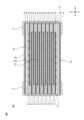
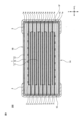
- FIG. 1 is a perspective view of a multilayer ceramic capacitor 100. 1 is a cross-sectional view of a multilayer ceramic capacitor 100. FIG. 1 is a cross-sectional view of a multilayer ceramic capacitor 100. FIG. 1 is a cross-sectional view of a multilayer ceramic capacitor 200. FIG.
- each embodiment is an illustrative example of how the present invention can be implemented, and the present invention is not limited to the contents of the embodiment. It is also possible to combine the contents described in different embodiments, and the implementation in such cases is also included in the present invention.
- the drawings are intended to aid in understanding the specification, and may be drawn diagrammatically, and the dimensional ratios of the depicted components or between the components may not match those dimensional ratios described in the specification. Components described in the specification may be omitted in the drawings, or may be drawn with the number of components omitted.
- FIG. 1 is a perspective view of the multilayer ceramic capacitor 100.
- FIG. 2 is a cross-sectional view of the multilayer ceramic capacitor 100, showing a portion II-II indicated by an alternate long and short dashed arrow in FIG. 1.
- FIG. 3 is also a cross-sectional view of the multilayer ceramic capacitor 100, showing a portion III-III indicated by an alternate long and short dashed arrow in FIG. 1.
- the height direction T, width direction W, and length direction L of the multilayer ceramic capacitor 100 are shown in the figures, and these directions may be referred to in the following description.
- the stacking direction of ceramic layers 1a which will be described later, is defined as the height direction T of the multilayer ceramic capacitor 100.
- the multilayer ceramic capacitor 100 has a ceramic body 1 having a rectangular parallelepiped shape.
- the ceramic body 1 has a first main surface 1A and a second main surface 1B that face each other in a height direction T, a first side surface 1C and a second side surface 1D that face each other in a width direction W that is perpendicular to the height direction T, and a first end surface 1E and a second end surface 1F that face each other in a length direction L that is perpendicular to both the height direction T and the width direction W.
- the ceramic body 1 includes a plurality of ceramic layers 1a, a plurality of first internal electrodes 2, and a plurality of second internal electrodes 3 stacked in the height direction T.
- the first internal electrodes 2 are extended to a first end surface 1E of the ceramic body 1.
- the second internal electrodes 3 are extended to a second end surface 1F of the ceramic body 1.
- the thickness of the ceramic layer 1a is arbitrary, but for example, in the capacitance forming portion 11 described below, it can be about 0.3 ⁇ m to 2.0 ⁇ m.
- the ceramic body 1 includes a capacitance forming portion 11 that contributes to the formation of capacitance, in which a first internal electrode 2 and a second internal electrode 3 are arranged facing each other with a ceramic layer 1a interposed therebetween.
- the capacitance forming portion 11 is shown by a two-dot chain line in each of Figures 2 and 3.
- the capacitance forming portion 11 is in the shape of a rectangular parallelepiped having six sides.
- the ceramic body 1 includes non-capacitance forming portions 12 that do not contribute to the formation of capacitance, which are formed on the outer sides of the six faces of the capacitance forming portion 11 and in which the first internal electrode 2 and the second internal electrode 3 are not arranged opposite each other via the ceramic layer 1a.
- the non-capacitance forming portions 12 formed on the outer sides of the first main surface 1A and the second main surface 1B of the capacitance forming portion 11 may be called protective layers. Note that the protective layer has a larger area than the capacitance forming portion 11 when viewed in the planar direction.
- the non-capacitance forming portions 12 formed on the outer sides of the first side surface 1C and the second side surface 1D of the capacitance forming portion 11 may be called side gaps.
- the non-capacitance forming portions 12 formed on the outer sides of the first end surface 1E and the second end surface 1F of the capacitance forming portion 11 may be called pull-out portions (pull-out portions of the internal electrodes).
- the ceramic body 1 includes a surface protective layer 13 formed on at least a portion of the outside of the non-capacity forming portion 12 and exposed at least to the first main surface 1A, the second main surface 1B, the first side surface 1C, and the second side surface 1D.
- the surface protective layer 13 is formed on the outside of the first main surface 1A side, the second main surface 1B side, the first side surface 1C side, and the second side surface 1D side of the non-capacity forming portion 12, respectively, and is not formed on the outside of the first end surface 1E side and the second end surface 1F side of the non-capacity forming portion 12.
- the ceramic composition of the surface protective layer 13 is different from that of the ceramic composition of the non-capacity forming portion 12.
- the surface protective layer 13 is formed continuously on the outside of the first main surface 1A side, the second main surface 1B side, the first side surface 1C side, and the second side surface 1D side of the non-capacity forming portion 12.
- the ceramic constituting the capacitance forming portion 11 of the ceramic body 1 is made of ceramic having a composition suitable for realizing a good dielectric constant.
- the type of ceramic constituting the capacitance forming portion 11 is arbitrary, but for example, a dielectric ceramic containing BaTiO3 as a main component can be used.
- a dielectric ceramic containing BaTiO3 as a main component is used for the ceramic constituting the capacitance forming portion 11.
- a dielectric ceramic containing another material as a main component such as CaTiO3 , SrTiO3 , or CaZrO3 , may be used.
- the type of ceramic constituting the non-capacitance forming portion 12 of the ceramic body 1 is arbitrary, but it is preferable to use the same ceramic as that constituting the capacitance forming portion 11.
- the ceramic constituting the non-capacitance forming portion 12 is a dielectric ceramic mainly composed of BaTiO3 , the same as that of the capacitance forming portion 11.
- the ceramic constituting the surface protective layer 13 of the ceramic body 1 is a ceramic that exhibits high strength.
- the type of ceramic constituting the surface protective layer 13 is arbitrary, but in this embodiment, particles having a core-shell structure in which Zr (zirconium) is contained as a shell on the surface of BaTiO 3 are used as the main component of the ceramic constituting the surface protective layer 13.
- a composite of ZrO 2 (zirconium oxide; zirconia) and BaTiO 3 may be used instead of (or in addition to) particles having a core-shell structure in which Zr is contained as a shell on the surface of BaTiO 3 .
- a ceramic containing particles having a core-shell structure in which Zr is contained as a shell on the surface of BaTiO 3 , or a ceramic made of a composite of ZrO 2 and BaTiO 3 can exhibit high strength.
- the type of metal that is the main component of the first internal electrode 2 and the second internal electrode 3 is arbitrary, and for example, Ni can be used. However, other metals such as Cu, Ag, Pd, and Au may be used instead of Ni. Furthermore, Ni, Cu, Ag, Pd, and Au may be alloyed with other metals.
- the thickness of the first internal electrode 2 and the second internal electrode 3 is arbitrary, but it is preferable that it is, for example, about 0.1 to 2.0 ⁇ m.
- the multilayer ceramic capacitor 100 has a first external electrode 4 formed on one end of the ceramic body 1, and a second external electrode 5 formed on the other end of the ceramic body 1. More specifically, the first external electrode 4 is formed on the first end face 1E of the ceramic body 1, and has a cap shape with edges extending to the first main face 1A, the second main face 1B, the first side face 1C, and the second side face 1D.
- the second external electrode 5 is formed on the second end face 1F of the ceramic body 1, and has a cap shape with edges extending to the first main face 1A, the second main face 1B, the first side face 1C, and the second side face 1D.
- the first external electrode 4 and the second external electrode 5 are each shown as one layer. However, in general, the first external electrode 4 and the second external electrode 5 are formed in multiple layers. The number of layers, materials, dimensions, and formation method of the first external electrode 4 and the second external electrode 5 are arbitrary. In this embodiment, the first external electrode 4 and the second external electrode 5 are each formed of three layers: a base electrode layer mainly composed of Cu formed by baking a Cu conductive paste, a Ni-plated electrode layer formed on the base electrode layer, and a Sn-plated electrode layer formed on the Ni-plated electrode layer. However, the main component of the base electrode layer may be, for example, Ni or Ag instead of Cu. In addition, Cu, Ni, Ag, and the like may be alloys with other metals. In the first external electrode 4 and the second external electrode 5, the Ni-plated electrode layer is provided mainly to improve the solder heat resistance and the bondability. The Sn-plated electrode layer on the first external electrode 4 and the second external electrode 5 is provided primarily to improve solderability.
- the first internal electrode 2 is electrically connected to the first external electrode 4.
- the second internal electrode 3 is electrically connected to the second external electrode 5.
- the laminated ceramic capacitor 100 configured as described above uses ceramics of different compositions for the surface protective layer 13 of the ceramic body 1 and for the capacitance forming portion 11 and non-capacitance forming portion 12, so that the strength of the ceramic body 1 can be maintained by using a ceramic of a composition that exhibits high strength for the surface protective layer 13.
- the laminated ceramic capacitor 100 uses ceramics of different compositions for the surface protective layer 13 of the ceramic body 1 and for the capacitance forming portion 11 and non-capacitance forming portion 12, so that a high capacitance can be exhibited by using a ceramic of a composition that exhibits a high dielectric constant for the capacitance forming portion 11 and non-capacitance forming portion 12.
- the surface protection layer 13 of the ceramic body 1 of the multilayer ceramic capacitor 100 has high strength, even if an external force is applied to the ceramic body 1, the ceramic body 1 is unlikely to crack or break, and has high moisture resistance reliability.
- the ceramic constituting the surface protective layer 13 preferably contains Zr (zirconia). Also, in the multilayer ceramic capacitor 100, the ceramic constituting the surface protective layer 13 preferably contains ZrO2 (zirconium oxide; zirconia), and it is more preferable that the ZrO2 contained is stabilized ZrO2 . In these cases, even if an external force is applied to the ceramic body 1, the occurrence of cracks or chips in the ceramic body 1 due to stress-induced phase transition of Zr or ZrO2 can be more effectively suppressed.
- a ceramic including particles with a core-shell structure in which Zr is included as a shell on the surface of BaTiO3 can be used as the ceramic that constitutes the surface protective layer 13.
- a ceramic including a composite of ZrO2 and BaTiO3 can be used as the ceramic that constitutes the surface protective layer 13. In these cases, a surface protective layer 13 with even higher strength can be formed.
- the average grain size of the ceramic that constitutes the surface protective layer 13 is smaller than the average grain size of the ceramic that constitutes the non-capacitance forming portion 12. This is because the strength of the surface protective layer 13 is further improved by being formed from ceramic with a small average grain size.
- the average grain size of the ceramic that constitutes the surface protective layer 13 can be adjusted by adjusting the grain size and amount of the raw material used to form the surface protective layer 13, the type and amount of additives added to the raw material, etc.
- the average grain size of the ceramic constituting the non-capacitance forming portion 12 and the surface protective layer 13 is measured by the following method. First, one surface is arbitrarily selected from the first main surface 1A, the second main surface 1B, the first side surface 1C, and the second side surface 1D of the ceramic body 1. Next, the thickness of the non-capacitance forming portion 12 and the thickness of the surface protective layer 13 are measured on that surface. Next, at the center of that surface (the point where the two diagonals intersect), a cross section parallel to that surface is cut out to a depth of 1/2 the total thickness of the surface protective layer 13, and a square area of 30 ⁇ m x 30 ⁇ m is obtained, which is the measurement area of the surface protective layer 13.
- a cross section parallel to that surface is cut out to a depth of 1/2 the total thickness of the non-capacitance forming portion 12, and a square area of 30 ⁇ m x 30 ⁇ m is obtained, which is the measurement area of the non-capacitance forming portion 12.
- the measurement area (cross section) of the surface protective layer 13 is observed with an electron microscope, and of the particles that appear in the measurement area, 10 particles are selected in order of diameter from the largest, and the average value of the diameters of these particles is simply taken as the average particle diameter of the ceramic that constitutes the surface protective layer 13.
- the measurement area (cross section) of the non-capacity forming portion 12 is observed with an electron microscope, and of the particles that appear in the measurement area, 10 particles are selected in order of diameter from the largest, and the average value of the diameters of these particles is simply taken as the average particle diameter of the ceramic that constitutes the non-capacity forming portion 12.
- the average particle size of the ceramic that constitutes the surface protection layer 13 is preferably 0.35 ⁇ m or less. This is because if it is 0.35 ⁇ m or less, the surface protection layer 13 has high strength.
- the pore ratio of the ceramic that constitutes the surface protective layer 13 is greater than the pore ratio of the ceramic that constitutes the non-capacitance forming portion 12. If the pore ratio of the ceramic that constitutes the surface protective layer 13 is high, the pores (voids) contained in the surface protective layer 13 can disperse the stress applied to the ceramic body 1, and the stress can be prevented from being propagated to the non-capacitance forming portion 12 or the capacitance forming portion 11.
- the pore ratio of the ceramic that constitutes the surface protective layer 13 can be adjusted by adjusting the particle size and amount of the raw material used to form the surface protective layer 13, the type and amount of additives added to the raw material, etc.
- the pore ratio of the ceramics constituting the non-capacitance forming portion 12 and the surface protective layer 13 is measured by the following method. First, one surface is arbitrarily selected from the first main surface 1A, the second main surface 1B, the first side surface 1C, and the second side surface 1D of the ceramic body 1. Next, the thickness of the non-capacitance forming portion 12 and the thickness of the surface protective layer 13 on that surface are measured. Next, a cross section is cut out at the center of that surface, parallel to that surface, to a depth of 1/2 the total thickness of the surface protective layer 13, and a square area of 1 ⁇ m x 1 ⁇ m is obtained, which is the measurement area of the surface protective layer 13.
- a cross section is cut out at the center of that surface, parallel to that surface, to a depth of 1/2 the total thickness of the non-capacitance forming portion 12, and a square area of 1 ⁇ m x 1 ⁇ m is obtained, which is the measurement area of the non-capacitance forming portion 12.
- the number of pore sections ⁇ 10,000 x 100 (%) is simply defined as the pore ratio of the ceramic that constitutes the surface protective layer 13.
- the number of pore sections ⁇ 10,000 x 100 (%) is simply defined as the pore ratio of the ceramic that constitutes the non-capacity forming portion 12.
- the average thickness of the surface protective layer 13 is 1 ⁇ m or more and 10 ⁇ m or less. If the average thickness of the surface protective layer 13 is less than 1 ⁇ m, there is a risk that the surface protective layer 13 will not be able to adequately protect the ceramic body 1. If the average thickness of the surface protective layer 13 exceeds 10 ⁇ m, the dimensions of the ceramic body 1 will become larger than necessary.
- the average thickness of the surface protective layer 13 is determined by measuring the thickness of the surface protective layer 13 at the center of each of the four faces of the ceramic body 1, namely the first main face 1A, the second main face 1B, the first side face 1C, and the second side face 1D, and averaging these four thicknesses.
- the multilayer ceramic capacitor 100 can be manufactured, for example, by the following method.
- ceramic powder, binder resin, solvent, etc. are prepared and wet-mixed to prepare ceramic slurry.
- BaTiO3 powder is used as the ceramic powder.
- the ceramic slurry is applied in sheet form onto a carrier film using a die coater, gravure coater, microgravure coater, etc., and then dried to produce a mother ceramic green sheet.
- a large number of ceramic green sheets for the multilayer ceramic capacitors are arranged in a matrix on the mother ceramic green sheet.
- a conductive paste prepared in advance is applied (e.g., printed) in a desired pattern shape to the main surface of a predetermined mother ceramic green sheet in order to form a first internal electrode 2.
- a conductive paste prepared in advance is also applied in a desired pattern shape to the main surface of a predetermined mother ceramic green sheet in order to form a second internal electrode 3. Note that no conductive paste is applied to the main surface of the predetermined mother ceramic green sheet for forming a protective layer.
- the conductive paste can be, for example, a mixture of metal powder (e.g., Ni powder), a solvent, a binder resin, etc.
- the unfired mother ceramic body contains a large number of unfired ceramic bodies in a matrix.
- the unsintered mother ceramic body is cut into strips to produce a group of unsintered strip-shaped ceramic bodies.
- the group of unsintered strip-shaped ceramic bodies has the first end face and second end face connected between adjacent unsintered ceramic bodies such that the first main face, second main face, first side face, and second side face of each unsintered ceramic body are exposed to the outside.
- elemental powder and/or ceramic powder are applied to the outer surfaces of the unsintered rectangular ceramic element body group. That is, raw materials for forming the surface protective layer 13 are applied to the outer surfaces of the unsintered rectangular ceramic element body group.
- Zr powder is applied as the elemental powder and/or ZrO2 powder is applied as the ceramic powder.
- additives such as binder resin and solvent may be added to the powder to facilitate the application.
- the group of unsintered rectangular ceramic elements is cut into individual unsintered ceramic elements.
- An element powder e.g., Zr powder
- a ceramic powder e.g., ZrO2 powder
- the unsintered ceramic elements at both ends of the group of unsintered rectangular ceramic elements are preferably discarded because unnecessary powder may be attached to the first end surface and second end surface.
- the unfired ceramic body is fired with a predetermined profile to produce the ceramic body 1.
- the element powder (Zr powder) and/or ceramic powder (ZrO 2 powder) reacts with or is mixed with the ceramic contained in the unfired ceramic body (ceramic green sheet) to form a surface protective layer 13 on the first main surface 1A, the second main surface 1B, the first side surface 1C, and the second side surface 1D of the ceramic body 1.
- the surface protective layer 13 is formed by, for example, particles with a core-shell structure containing Zr as a shell on the surface of BaTiO 3 , or ceramics containing a composite of ZrO 2 and BaTiO 3.
- the form of the ceramic constituting the surface protective layer 13 is not limited to these forms.
- a base electrode layer is formed on both ends of the ceramic body 1, for example by baking a Cu conductive paste, a Ni-plated electrode layer is formed on the base electrode layer, and a Sn-plated electrode layer is formed on the Ni-plated electrode layer, thereby forming a first external electrode 4 and a second external electrode 5, and the multilayer ceramic capacitor 100 is completed.
- FIG. 4 shows a multilayer ceramic capacitor 200 according to the second embodiment. Note that FIG. 4 is a perspective view of the multilayer ceramic capacitor 200.
- the multilayer ceramic capacitor 200 according to the second embodiment is obtained by adding a change to a part of the configuration of the multilayer ceramic capacitor 100 according to the first embodiment.
- the surface protective layer 13 is formed on the first main surface 1A, the second main surface 1B, the first side surface 1C, and the second side surface 1D of the ceramic body 1.
- this is changed, and the surface protective layer 13 is formed on the first main surface 1A, the second main surface 1B, the first side surface 1C, the second side surface 1D, the first end surface, and the second end surface of the ceramic body 1.
- the surface protective layer 13 is continuously formed on the first main surface 1A, the second main surface 1B, the first side surface 1C, the second side surface 1D, the first end surface, and the second end surface of the ceramic body 1.
- the raw material powder for forming the surface protective layer 13 is applied to the outer surface of the group of unsintered rectangular ceramic bodies.
- the surface protective layer 13 will also be formed on the first end face and second end face of the ceramic body 1, as in the multilayer ceramic capacitor 200.
- the multilayer ceramic capacitor 200 according to the second embodiment has improved strength at the first and second end faces of the ceramic body 1.
- the ceramic materials constituting the capacitance forming portion 11, the non-capacitance forming portion 12, and the surface protective layer 13 of the ceramic body 1 described above are merely examples, and other materials may also be used.
- the form of the ceramic contained in the surface protection layer 13 (such as a core-shell structure or a composite) is also an example and is not limited to the above.
- the multilayer ceramic capacitor according to one embodiment of the present invention is as described in the "Means for solving the problems" section.
- the composition of the ceramic that constitutes the capacitance forming portion is the same as the composition of the ceramic that constitutes the non-capacitance forming portion.
- the multilayer ceramic capacitor can be manufactured using one type of ceramic green sheet, improving productivity.
- material procurement, material processing, and material management become easier, improving productivity.
- the ceramic constituting the surface protective layer contains Zr.
- the ceramic constituting the surface protective layer contains ZrO2 .
- the ceramic constituting the surface protective layer contains particles with a core-shell structure in which Zr is contained as a shell on the surface of BaTiO3 .
- the ceramic constituting the surface protective layer contains a composite of ZrO2 and BaTiO3 . In these cases, even if an external force is applied to the ceramic body, the occurrence of cracks or chips in the ceramic body 1 can be effectively suppressed due to the stress-induced phase transition of Zr or ZrO2 .
- the average grain size of the ceramic that constitutes the surface protection layer is smaller than the average grain size of the ceramic that constitutes the non-capacitor forming portion.
- the surface protection layer is formed from ceramic with a small average grain size, which further improves the strength of the ceramic cutting.
- the average particle size of the ceramic that makes up the surface protection layer is 0.35 ⁇ m or less. In this case, the surface protection layer has high strength.
- the pore ratio of the ceramic that constitutes the surface protective layer is greater than the pore ratio of the ceramic that constitutes the non-capacity forming parts.
- the stress applied to the ceramic body can be dispersed by the pores (voids) contained in the surface protective layer, and the stress can be prevented from being transmitted to the non-capacity forming parts or the capacitance forming parts.
- the average thickness of the surface protection layer is 1 ⁇ m or more and 10 ⁇ m or less. If the average thickness of the surface protection layer is less than 1 ⁇ m, there is a risk that the surface protection layer will not be able to adequately protect the ceramic body 1. If the average thickness of the surface protection layer exceeds 10 ⁇ m, the dimensions of the ceramic body 1 will be larger than necessary.
- the method for manufacturing a multilayer ceramic capacitor according to one embodiment of the present invention is as described in the "Means for solving the problems" section.
- the element powder attached to the green ceramic body is Zr.
- the ceramic powder attached to the green ceramic body is ZrO2 . In these cases, a surface protection layer with high strength can be formed on the ceramic body.
Landscapes
- Engineering & Computer Science (AREA)
- Chemical & Material Sciences (AREA)
- Power Engineering (AREA)
- Ceramic Engineering (AREA)
- Manufacturing & Machinery (AREA)
- Microelectronics & Electronic Packaging (AREA)
- Materials Engineering (AREA)
- Inorganic Chemistry (AREA)
- Organic Chemistry (AREA)
- Structural Engineering (AREA)
- Composite Materials (AREA)
- Ceramic Capacitors (AREA)
- Fixed Capacitors And Capacitor Manufacturing Machines (AREA)
Priority Applications (3)
| Application Number | Priority Date | Filing Date | Title |
|---|---|---|---|
| JP2025506535A JPWO2024190114A1 (https=) | 2023-03-11 | 2024-01-27 | |
| CN202480011311.XA CN120584389A (zh) | 2023-03-11 | 2024-01-27 | 层叠陶瓷电容器以及层叠陶瓷电容器的制造方法 |
| US19/196,117 US20250259792A1 (en) | 2023-03-11 | 2025-05-01 | Multilayer ceramic capacitor and manufacturing method of multilayer ceramic capacitor |
Applications Claiming Priority (2)
| Application Number | Priority Date | Filing Date | Title |
|---|---|---|---|
| JP2023038186 | 2023-03-11 | ||
| JP2023-038186 | 2023-03-11 |
Related Child Applications (1)
| Application Number | Title | Priority Date | Filing Date |
|---|---|---|---|
| US19/196,117 Continuation US20250259792A1 (en) | 2023-03-11 | 2025-05-01 | Multilayer ceramic capacitor and manufacturing method of multilayer ceramic capacitor |
Publications (1)
| Publication Number | Publication Date |
|---|---|
| WO2024190114A1 true WO2024190114A1 (ja) | 2024-09-19 |
Family
ID=92754560
Family Applications (1)
| Application Number | Title | Priority Date | Filing Date |
|---|---|---|---|
| PCT/JP2024/002538 Ceased WO2024190114A1 (ja) | 2023-03-11 | 2024-01-27 | 積層セラミックコンデンサおよび積層セラミックコンデンサの製造方法 |
Country Status (4)
| Country | Link |
|---|---|
| US (1) | US20250259792A1 (https=) |
| JP (1) | JPWO2024190114A1 (https=) |
| CN (1) | CN120584389A (https=) |
| WO (1) | WO2024190114A1 (https=) |
Citations (4)
| Publication number | Priority date | Publication date | Assignee | Title |
|---|---|---|---|---|
| JPH07288217A (ja) * | 1994-04-18 | 1995-10-31 | Matsushita Electric Ind Co Ltd | 積層セラミックコンデンサの製造方法 |
| JPH08181029A (ja) * | 1994-12-26 | 1996-07-12 | Taiyo Yuden Co Ltd | 電子部品の製造方法 |
| WO2012046554A1 (ja) * | 2010-10-04 | 2012-04-12 | 株式会社村田製作所 | 積層セラミックコンデンサおよびその製造方法 |
| JP2022170166A (ja) * | 2021-04-28 | 2022-11-10 | Tdk株式会社 | 電子部品 |
-
2024
- 2024-01-27 JP JP2025506535A patent/JPWO2024190114A1/ja active Pending
- 2024-01-27 CN CN202480011311.XA patent/CN120584389A/zh active Pending
- 2024-01-27 WO PCT/JP2024/002538 patent/WO2024190114A1/ja not_active Ceased
-
2025
- 2025-05-01 US US19/196,117 patent/US20250259792A1/en active Pending
Patent Citations (4)
| Publication number | Priority date | Publication date | Assignee | Title |
|---|---|---|---|---|
| JPH07288217A (ja) * | 1994-04-18 | 1995-10-31 | Matsushita Electric Ind Co Ltd | 積層セラミックコンデンサの製造方法 |
| JPH08181029A (ja) * | 1994-12-26 | 1996-07-12 | Taiyo Yuden Co Ltd | 電子部品の製造方法 |
| WO2012046554A1 (ja) * | 2010-10-04 | 2012-04-12 | 株式会社村田製作所 | 積層セラミックコンデンサおよびその製造方法 |
| JP2022170166A (ja) * | 2021-04-28 | 2022-11-10 | Tdk株式会社 | 電子部品 |
Also Published As
| Publication number | Publication date |
|---|---|
| CN120584389A (zh) | 2025-09-02 |
| JPWO2024190114A1 (https=) | 2024-09-19 |
| US20250259792A1 (en) | 2025-08-14 |
Similar Documents
| Publication | Publication Date | Title |
|---|---|---|
| JP6439551B2 (ja) | 積層セラミックコンデンサ | |
| JP7296744B2 (ja) | 積層セラミックコンデンサ及びその製造方法 | |
| KR100908984B1 (ko) | 적층세라믹 전자부품 | |
| KR101397835B1 (ko) | 적층 세라믹 전자부품 및 이의 제조방법 | |
| JP7196732B2 (ja) | 積層セラミックコンデンサおよび積層セラミックコンデンサの製造方法 | |
| JP2020068227A (ja) | 積層セラミック電子部品 | |
| KR102415350B1 (ko) | 적층 세라믹 전자부품, 및 적층 세라믹 전자부품의 제조 방법 | |
| JP7183051B2 (ja) | 積層セラミックコンデンサ及び積層セラミックコンデンサの製造方法 | |
| KR102307161B1 (ko) | 적층 세라믹 전자부품 | |
| JP2000049033A (ja) | セラミック電子部品 | |
| JP3350949B2 (ja) | 導電性ペースト | |
| KR101434103B1 (ko) | 적층 세라믹 전자부품 및 적층 세라믹 전자부품의 실장 기판 | |
| KR100676035B1 (ko) | 적층 세라믹 콘덴서 | |
| WO2011114808A1 (ja) | 積層セラミック電子部品 | |
| JP7697536B2 (ja) | 電子部品 | |
| JP7493322B2 (ja) | 積層セラミックコンデンサ | |
| JPH05190375A (ja) | 銅多層セラミック基板の製造方法及びそれに用いる銅ペースト | |
| KR102303314B1 (ko) | 적층 세라믹 전자부품 | |
| JP2009246105A (ja) | 積層コンデンサ | |
| WO2024190114A1 (ja) | 積層セラミックコンデンサおよび積層セラミックコンデンサの製造方法 | |
| JPH04260314A (ja) | セラミック積層体 | |
| WO2011114809A1 (ja) | 積層セラミック電子部品 | |
| WO2011114807A1 (ja) | 積層セラミック電子部品 | |
| WO2011114804A1 (ja) | 積層セラミック電子部品 | |
| JP2006202857A (ja) | 積層セラミック電子部品および積層セラミック電子部品の製造方法 |
Legal Events
| Date | Code | Title | Description |
|---|---|---|---|
| 121 | Ep: the epo has been informed by wipo that ep was designated in this application |
Ref document number: 24770234 Country of ref document: EP Kind code of ref document: A1 |
|
| WWE | Wipo information: entry into national phase |
Ref document number: 2025506535 Country of ref document: JP |
|
| WWE | Wipo information: entry into national phase |
Ref document number: 202480011311.X Country of ref document: CN |
|
| WWP | Wipo information: published in national office |
Ref document number: 202480011311.X Country of ref document: CN |
|
| NENP | Non-entry into the national phase |
Ref country code: DE |
|
| 122 | Ep: pct application non-entry in european phase |
Ref document number: 24770234 Country of ref document: EP Kind code of ref document: A1 |