WO2024181272A1 - 基板、電子装置、及び、基板の製造方法 - Google Patents
基板、電子装置、及び、基板の製造方法 Download PDFInfo
- Publication number
- WO2024181272A1 WO2024181272A1 PCT/JP2024/006299 JP2024006299W WO2024181272A1 WO 2024181272 A1 WO2024181272 A1 WO 2024181272A1 JP 2024006299 W JP2024006299 W JP 2024006299W WO 2024181272 A1 WO2024181272 A1 WO 2024181272A1
- Authority
- WO
- WIPO (PCT)
- Prior art keywords
- mounting surface
- substrate
- recess
- metallization layer
- recesses
- Prior art date
- Legal status (The legal status is an assumption and is not a legal conclusion. Google has not performed a legal analysis and makes no representation as to the accuracy of the status listed.)
- Ceased
Links
Images






Classifications
-
- H—ELECTRICITY
- H03—ELECTRONIC CIRCUITRY
- H03H—IMPEDANCE NETWORKS, e.g. RESONANT CIRCUITS; RESONATORS
- H03H3/00—Apparatus or processes specially adapted for the manufacture of impedance networks, resonating circuits, resonators
- H03H3/007—Apparatus or processes specially adapted for the manufacture of impedance networks, resonating circuits, resonators for the manufacture of electromechanical resonators or networks
- H03H3/02—Apparatus or processes specially adapted for the manufacture of impedance networks, resonating circuits, resonators for the manufacture of electromechanical resonators or networks for the manufacture of piezoelectric or electrostrictive resonators or networks
-
- H—ELECTRICITY
- H03—ELECTRONIC CIRCUITRY
- H03H—IMPEDANCE NETWORKS, e.g. RESONANT CIRCUITS; RESONATORS
- H03H9/00—Networks comprising electromechanical or electro-acoustic elements; Electromechanical resonators
- H03H9/02—Details
- H03H9/05—Holders or supports
- H03H9/10—Mounting in enclosures
-
- H—ELECTRICITY
- H10—SEMICONDUCTOR DEVICES; ELECTRIC SOLID-STATE DEVICES NOT OTHERWISE PROVIDED FOR
- H10W—GENERIC PACKAGES, INTERCONNECTIONS, CONNECTORS OR OTHER CONSTRUCTIONAL DETAILS OF DEVICES COVERED BY CLASS H10
- H10W70/00—Package substrates; Interposers; Redistribution layers [RDL]
- H10W70/60—Insulating or insulated package substrates; Interposers; Redistribution layers
Definitions
- This disclosure relates to a substrate equipped with connection electrodes that connect to a connection target.
- Patent Document 1 discloses an insulating substrate having a pair of electrode pads coated with band-shaped bumps extending in the width direction of the piezoelectric substrate in order to hold the quartz crystal piece afloat above the package or substrate.
- the electrode pads disclosed in Patent Document 1 are formed by printing a conductor that serves as the base conductor of the electrode pads using a metal paste, drying it, and then printing a bump-shaped conductor on the surface using a metal paste, and then firing both of them.
- a substrate includes an insulating substrate having a mounting surface on which a connection object is mounted and one or more recesses opening into the mounting surface, a connection electrode connected to the connection object, and the connection electrode has an underlying metallization layer that extends along the bottom surface of the recess and also extends along at least a portion of the wall surface of the recess to reach the mounting surface, and a plating layer that covers the exposed surface of the underlying metallization layer.
- An electronic device includes a substrate according to one aspect of the present disclosure, a piezoelectric vibration element connected to the substrate via a conductive bonding material, and a lid provided on the substrate so as to cover the piezoelectric vibration element.
- the method for manufacturing a substrate according to one embodiment of the present disclosure includes a pressurizing step in which an insulating material having a base metallization pattern on its surface is pressed with a mold to form an insulating substrate having a mounting surface on which a connection target is mounted and one or more recesses opening into the mounting surface, and a base metallization layer that extends along the bottom surface of the recess and also extends along at least a portion of the wall surface of the recess to reach the mounting surface, and a plating layer formation step in which a plating layer is formed to cover the exposed surface of the base metallization layer.
- FIG. 1 is a cross-sectional view of a piezoelectric device according to a first embodiment.
- FIG. 2 is a plan view of a substrate included in the piezoelectric device.
- 11 is a cross-sectional view of a modified example of the substrate.
- FIG. 11 is a cross-sectional view of another modified example of the substrate.
- FIG. 11 is a cross-sectional view of yet another modified example of the substrate.
- FIG. 11 is a cross-sectional view of yet another modified example of the substrate.
- FIG. 11 is a cross-sectional view of yet another modified example of the substrate.
- FIG. 11 is a cross-sectional view of yet another modified example of the substrate.
- FIG. 11 is a plan view of a substrate according to a second embodiment.
- FIG. 13 is a plan view of a modified example of the substrate.
- FIG. 10 is a cross-sectional view taken along line XX shown in FIG. 9.
- FIG. 13 is a plan view of another modified example of the substrate.
- FIG. 11 is a cross-sectional view of a piezoelectric device according to a third embodiment.
- FIG. 11 is a cross-sectional view of a modified example of the piezoelectric device.
- 5A to 5C are cross-sectional views showing a method for manufacturing a substrate.
- 5A to 5C are cross-sectional views showing a method for manufacturing a substrate.
- top and bottom in the following description is for convenience and does not limit the top and bottom when the substrate 1 and the piezoelectric device 11 are actually used.
- the surface of the insulating substrate 2 or substrate 1 on which the piezoelectric vibration element 6 is mounted is defined as the top surface.
- the positive direction of the Z axis is the upward direction.
- the X axis is the longitudinal direction of the insulating substrate 2 or substrate 1
- the Y axis is an axis that intersects perpendicularly with the X axis and the Z axis.
- One aspect of the present disclosure aims to realize a substrate, an electronic device, and a method for manufacturing a substrate, in which the dimensional accuracy and shape of the bumps are stable.
- a substrate an electronic device, and a method for manufacturing a substrate, in which the dimensional accuracy and shape of the bumps are stable.
- Fig. 1 is a cross-sectional view of a piezoelectric device 11 according to embodiment 1.
- Fig. 2 is a plan view of a substrate 1 included in the piezoelectric device 11.
- the piezoelectric device 11 is an example of an electronic device according to the present disclosure.
- the piezoelectric device 11 includes a substrate 1, a piezoelectric vibration element 6 connected to the substrate 1 via a conductive bonding material 7, and a lid 8 provided on the substrate 1 to cover the piezoelectric vibration element 6.
- the piezoelectric vibration element 6 is an example of a connection subject according to the present disclosure.
- the conductive bonding material 7 may be a bonding material in which Ag powder or the like is added to a resin such as a silicone-based, epoxy-based, or polyimide-based resin. Alternatively, the conductive bonding material 7 may be solder.
- the substrate 1 has an insulating substrate 2 having a mounting surface 2a on which the piezoelectric vibration element 6 is mounted, a recess 2b opening into the mounting surface 2a, and a connection electrode 3 connected to the piezoelectric vibration element 6.
- the piezoelectric vibration element 6 is mechanically bonded and electrically connected to the connection electrode 3 of the substrate 1 via the conductive bonding material 7.
- the insulating substrate 2 has a flat base 2e and a frame 2f located on the upper surface of the base 2e.
- a frame-shaped metallization layer 10 is located on the upper surface of the frame 2f, i.e., the joint surface between the frame 2f and the lid 8.
- the frame-shaped metallization layer 10 is joined to the lid 8 using a sealing material such as a gold-tin alloy (AuSn) or silver solder.
- the mounting surface 2a corresponds to the bottom surface of the recess formed by the base 2e and the frame 2f of the insulating substrate 2.
- a plurality of external electrodes 9 are located on the lower surface of the insulating substrate 2.
- the lower surfaces of the external electrodes 9 and the lower surface of the insulating substrate 2 may be on the same plane.
- the connection electrodes 3 are electrically connected to the external electrodes 9 through wiring conductors (not shown) such as via conductors located in the insulating substrate 2.
- connection electrode 3 has an underlying metallization layer 4 that extends along the bottom surface 2c of the recess 2b and also extends along at least a portion of the wall surface 2d of the recess 2b to reach the mounting surface 2a, and a plating layer 5 that covers the exposed surface of the underlying metallization layer 4.
- the underlying metallization layer 4 is made of a metal containing, for example, tungsten (W) or molybdenum (Mo).
- the plating layer 5 contains, for example, nickel (Ni) or gold (Au).
- the base metallization layer 4 is provided, which extends along the bottom surface 2c of the recess 2b that opens into the mounting surface 2a of the insulating substrate 2 on which the piezoelectric vibration element 6 is mounted, and also extends along the wall surface 2d of this recess 2b to reach the mounting surface 2a.
- the base metallization layer 4 is then covered with the plating layer 5.
- connection electrode 3 which includes at least the plating layer 5 and has a convex shape relative to the mounting surface 2a, forms a bump for holding the piezoelectric vibration element 6 to be connected above the mounting surface 2a.
- the base metallization layer 4 has a bottom surface portion 4a that extends along the bottom surface 2c of the recess 2b, and a wall surface portion 4b that extends from the bottom surface portion 4a along the wall surface 2d of the recess 2b. In this way, the base metallization layer 4 has a wall surface portion 4b that extends upward from the bottom surface portion 4a to the mounting surface 2a.
- the piezoelectric vibration element 6 is connected via the conductive bonding material 7 and plating layer 5 at both the bottom surface portion 4a and the wall surface portion 4b, allowing for good electrical connection between the base metallization layer 4 and the piezoelectric vibration element 6.
- the mounting surface 2a may be rectangular in plan view with sides 2g and 2h that are parallel and opposed to each other, and sides 2i and 2j that are parallel and opposed to each other.
- the recesses 2b may be a pair of recesses 2b located along one short side 2g of the mounting surface 2a.
- the wall surface 2d of the recess 2b may be one of the four inner surfaces of the rectangular recess 2b that is located opposite the side 2g of the mounting surface 2a of the recess 2b.
- the substrate 1 is used as a substrate on which the piezoelectric vibration element 6, which requires cantilever support, is mounted.
- the upper surface of the plating layer 5 covering the bottom portion 4a is lower than the mounting surface 2a. Therefore, even if the piezoelectric vibration element 6 is mounted at a low position, the distance between the upper surface of the plating layer 5 located on the bottom portion 4a of the base metallization layer 4 and the lower surface of the piezoelectric vibration element 6 can be secured, and the conductive bonding material 7 can be configured to be thick. This reduces the risk of a decrease in the mechanical strength of the connection between the piezoelectric vibration element 6 and the substrate 1. Also, the risk of a short circuit between the conductive bonding material 7 corresponding to one of the pair of bumps and the conductive bonding material 7 corresponding to the other of the pair of bumps is reduced.
- the wall portion 4b may extend along the wall surface 2d of the recess 2b to a position on the same plane as the mounting surface 2a.
- the upper end of the wall portion 4b of the base metallization layer 4 located in the recess 2b may be at the same height as the mounting surface 2a.
- the plating layer 5 covering the exposed surface of the wall portion 4b which extends along the wall surface 2d of the recess 2b to the same plane as the mounting surface 2a, forms a bump with a fine height relative to the mounting surface 2a.
- the portion of the plating layer 5 covering the upper end of the wall portion 4b becomes a bump with a fine height that protrudes from the mounting surface 2a.
- the height of the bump can be adjusted by adjusting the thickness of the plating layer 5.
- the insulating substrate 2 is made of a ceramic material, such as an aluminum oxide sintered body, an aluminum nitride sintered body, a mullite sintered body, or a glass-ceramic sintered body.
- the insulating substrate 2 is described as being an aluminum oxide sintered body (alumina sintered body).
- the frame portion 2f and base portion 2e of the insulating substrate 2 are of an integral structure.
- the lid 8 is made of a conductive metal and is joined to the frame-shaped metallization layer 10 to hermetically seal the recess having the mounting surface 2a as its bottom surface.
- a conductive sealing member such as AuSn or silver solder is used for sealing.
- the lid 8 may be grounded. By grounding the lid 8, the propagation of external noise onto the mounting surface 2a can be reduced.
- the lid 8 is connected to the frame-shaped metallization layer 10 via the conductive sealing member.
- the frame-shaped metallization layer 10 is connected to the external electrode 9 via the internal frame wiring and via conductors. By grounding the external electrode 9, the lid 8 is in a grounded state.
- the frame-shaped metallization layer 10 is made of a conductive metal and is printed on the joint surface of the frame portion 2f.
- the frame-shaped metallization layer 10 and the exposed surfaces of the external electrodes 9 may be covered with a plating layer of nickel and/or gold.
- the exposed surfaces may be nickel-plated to a thickness of 1 to 20 ⁇ m, and a gold plating layer may be formed on the nickel plating layer to a thickness of 0.1 to 3.0 ⁇ m. This reduces the possibility of oxidation corrosion of the surface, and also makes it possible to easily and firmly connect the frame-shaped metallization layer 10 located on the top surface of the insulating substrate 2, which is an insulator, to the lid body 8, which is a metal conductor.
- the thickness of the base metallization layer 4 may be, for example, about 5 ⁇ m to 20 ⁇ m.
- the thickness of the plating layer 5 may be, for example, about 1 ⁇ m to 20 ⁇ m.
- the depth of the recess 2b may be, for example, about 10 ⁇ m to 30 ⁇ m.
- the protruding height (bump height) of the plating layer 5 from the mounting surface 2a may be, for example, about 5 ⁇ m to 30 ⁇ m.
- FIG. 3 is a cross-sectional view of a substrate 1A according to a modified example.
- the substrate 1A includes an insulating substrate 2 having a mounting surface 2a on which the piezoelectric vibration element 6 is mounted, a recess 2b opening into the mounting surface 2a, and a connection electrode 3A that connects to the piezoelectric vibration element 6.
- connection electrode 3A has an underlying metallization layer 4A including a bottom surface portion 4a extending along the bottom surface 2c of the recess 2b and a wall surface portion 4b extending from the bottom surface portion 4a along the wall surface 2d of the recess 2b, and a plating layer 5A covering the exposed surface of the underlying metallization layer 4A.
- the wall portion 4b of the base metallization layer 4A may extend along the wall surface 2d of the recess 2b to a position protruding from the mounting surface 2a. In this way, the base metallization layer 4A extends from the bottom surface 2c of the recess 2b along the wall surface 2d beyond the mounting surface 2a.
- the plating layer 5A covers the exposed surfaces of the wall portion 4b and the bottom portion 4a.
- the wall portion 4b which extends along the wall surface 2d of the recess 2b to a position where it protrudes from the mounting surface 2a, and the plating layer 5A form a bump that is convex with respect to the mounting surface 2a. Therefore, the wall portion 4b of the base metallization layer 4A forms a rough bump height, and the plating layer 5A can provide a highly accurate bump height. In addition, because the wall portion 4b protrudes from the mounting surface 2a, the thickness of the plating layer 5A in the bump can be made thinner, thereby reducing costs.
- the protruding height of the wall portion 4b of the base metallization layer 4A is also highly accurate when formed using a mold, as described below.
- FIG. 4 is a cross-sectional view of substrate 1B according to another modified example.
- the substrate 1B includes an insulating substrate 2 having a mounting surface 2a on which the piezoelectric vibration element 6 is mounted and a recess 2b opening into the mounting surface 2a, and a connection electrode 3B that connects to the piezoelectric vibration element 6.
- the connection electrode 3B has an underlying metallization layer 4B including a bottom surface portion 4a extending along the bottom surface 2c of the recess 2b, a wall surface portion 4b extending from the bottom surface portion 4a along the wall surface 2d of the recess 2b, and a mounting surface portion 4c extending from the wall surface portion 4b along a direction parallel to the mounting surface 2a, and a plating layer 5B covering the exposed surface of the underlying metallization layer 4B.
- the underlying metallization layer 4B may further include a mounting surface portion 4c extending from the wall surface portion 4b along a direction parallel to the mounting surface 2a. In this way, the mounting surface portion 4c of the underlying metallization layer 4B extends from the recess 2b.
- the plating layer 5B covers the exposed surface of the mounting surface portion 4c extending in a direction parallel to the mounting surface 2a. Therefore, at least a part of the connection electrode 3B that includes the plating layer 5B and has a convex shape relative to the mounting surface 2a forms a bump. Compared to the case where only the wall portion 4b protrudes as shown in FIG. 3, the width of the bump and the length of the bump extending along the mounting surface 2a can be made longer. As a result, the surface of the bump facing the piezoelectric vibration element 6 is larger, which stabilizes support of the piezoelectric vibration element 6 by the bump and improves the bonding strength between the bump and the piezoelectric vibration element 6. In addition, the conductive resistance between the bump and the piezoelectric vibration element 6 is improved.
- the insulating substrate 2 may also have a protruding portion 2k that protrudes from the mounting surface 2a adjacent to the recessed portion 2b.
- the wall portion 4b extends from the wall surface 2d of the recessed portion 2b onto the wall surface of the protruding portion 2k.
- the mounting surface portion 4c is located on the upper surface of the protruding portion 2k.
- the convex portion 2k, the mounting surface portion 4c located on the convex portion 2k, and the plating layer 5B form a bump that is convex with respect to the mounting surface 2a.
- the thicknesses of the base metallization layer 4B and plating layer 5B in the bump can be made thin.
- the combined protruding height of the convex portion 2k and the mounting surface portion 4c of the base metallization layer 4B is made highly accurate by forming it using a mold, which will be described later.
- the bump is formed by the thickness of the plating layer 5B above it, the bump height can be made highly accurate.
- FIG. 5 is a cross-sectional view of substrate 1C according to yet another modified example.
- the substrate 1C includes an insulating substrate 2 having a mounting surface 2a on which the piezoelectric vibration element 6 is mounted and a recess 2b opening into the mounting surface 2a, and a connection electrode 3C that connects to the piezoelectric vibration element 6.
- the connection electrode 3C has an underlying metallization layer 4C including a bottom surface portion 4a extending along the bottom surface 2c of the recess 2b, a wall surface portion 4b extending from the bottom surface portion 4a along the wall surface 2d of the recess 2b, and a mounting surface portion 4c extending from the wall surface portion 4b along a direction parallel to the mounting surface 2a, and a plating layer 5C covering the exposed surface of the underlying metallization layer 4C.
- the underlying metallization layer 4C may further include a mounting surface portion 4c extending from the wall surface portion 4b along a direction parallel to the mounting surface 2a. In this way, the mounting surface portion 4c of the underlying metallization layer 4C extends from the recess 2b.
- the plating layer 5C covers the exposed surface of the mounting surface portion 4c that extends in a direction parallel to the mounting surface 2a. Therefore, at least a portion of the connection electrode 3C that includes the plating layer 5C and has a convex shape relative to the mounting surface 2a forms a bump.
- the insulating substrate 2 has a convex portion 2m that protrudes from the mounting surface 2a adjacent to the recess 2b.
- the convex portion 2m has a middle stage portion 2n on the recess 2b side.
- the wall surface portion 4b extends from the wall surface 2d of the recess 2b along the wall surface of the convex portion 2m.
- the mounting surface portion 4c is located on the upper surface of the middle stage portion 2n of the convex portion 2m.
- the upper surface of the mounting surface portion 4c and the upper surface of the convex portion 2m may be on the same plane.
- the convex portion 2m, the mounting surface portion 4c located on the middle portion 2n of the convex portion 2m, and the plating layer 5C form a bump that is convex with respect to the mounting surface 2a. Since the insulating substrate 2 has the convex portion 2m, the base metallization layer 4C and the plating layer 5C can be made thin. If the conductive bonding material 7 is solder, the conductive bonding material 7 does not spread beyond the plating layer 4c and the convex portion 2m into the gap between the mounting surface 2a and the piezoelectric vibration element 6. This reduces the risk that the conductive bonding material 7 that has spread wet will affect the vibration of the piezoelectric vibration element 6.
- the support surface of the bump that supports the piezoelectric vibration element 6 is larger than that of the configuration shown in FIG. 4. This allows stable support of the piezoelectric vibration element 6, and increases the bonding strength between the piezoelectric vibration element 6 and the bump.
- the combined protruding height of the middle stage 2n of the protrusion 2m and the mounting surface 4c of the base metallization layer 4C is highly accurate by forming it using a mold described below.
- the bump is formed by the thickness of the plating layer 5C on top of that, so the bump height can be highly accurate.
- FIG. 6 is a cross-sectional view of substrate 1D relating to yet another modified example.
- the substrate 1D includes an insulating substrate 2 having a mounting surface 2a on which the piezoelectric vibration element 6 is mounted and a recess 2b opening into the mounting surface 2a, and a connection electrode 3D that connects to the piezoelectric vibration element 6.
- the connection electrode 3D has an underlying metallization layer 4D including a bottom surface portion 4a extending along the bottom surface 2c of the recess 2b, a wall surface portion 4b extending from the bottom surface portion 4a along the wall surface 2d of the recess 2b, and a mounting surface portion 4c extending from the wall surface portion 4b in a direction parallel to the mounting surface 2a, and a plating layer 5D covering the exposed surface of the underlying metallization layer 4D.
- the mounting surface portion 4c may extend over the mounting surface 2a. In this way, the mounting surface portion 4c of the underlying metallization layer 4D extends from the recess 2b to the mounting surface 2a.
- the mounting surface portion 4c and plating layer 5D extending above the mounting surface 2a form a bump that is convex with respect to the mounting surface 2a.
- the width of the bump and the length of the bump extending along the mounting surface 2a can be made longer.
- the surface of the bump facing the piezoelectric vibration element 6 is larger, so that the support of the piezoelectric vibration element 6 by the bump is stabilized and the bonding strength between the bump and the piezoelectric vibration element 6 is improved.
- the conductive resistance between the bump and the piezoelectric vibration element 6 is improved.
- the configuration shown in FIG. 6 as in the configuration shown in FIG.
- the protruding height of the mounting surface portion 4c of the base metallization layer 4D is formed with high precision by using a mold described later. Furthermore, since the bump is formed by the thickness of the plating layer 5D on top of it, the bump height can be made with high precision.
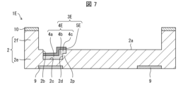
- FIG. 7 is a cross-sectional view of substrate 1E according to yet another modified example.
- the substrate 1E includes an insulating substrate 2 having a mounting surface 2a on which the piezoelectric vibration element 6 is mounted and a recess 2b opening into the mounting surface 2a, and a connection electrode 3E that connects to the piezoelectric vibration element 6.
- the connection electrode 3E has an underlying metallization layer 4E including a bottom surface portion 4a extending along the bottom surface 2c of the recess 2b, a wall surface portion 4b extending from the bottom surface portion 4a along the wall surface 2d of the recess 2b, and a mounting surface portion 4c extending from the wall surface portion 4b along a direction parallel to the mounting surface 2a, and a plating layer 5E covering the exposed surface of the underlying metallization layer 4E.
- the recess 2b has a middle step portion 2p located between the bottom surface 2c and the mounting surface 2a.
- the mounting surface portion 4c is located on the middle step portion 2p.
- the mounting surface portion 4c of the underlying metallization layer 4E extends from the bottom surface 2c of the recess 2b to the middle step portion 2p.
- the upper surface of the mounting surface portion 4c is on the same plane as the mounting surface 2a.
- the plating layer 5E covering the mounting surface portion 4c located on the middle portion 2p of the recess 2b forms a bump having a fine height relative to the mounting surface 2a.
- the height of the bump can be finely adjusted by adjusting the thickness of the plating layer 5E. Since the mounting surface portion 4c is provided in addition to the wall portion 4b, the plating layer 5E covering the wall portion 4b and mounting surface portion 4c of the base metallization layer 4E can be made longer than the configurations of Figures 1 and 3. This improves the bonding strength between the bump and the piezoelectric vibration element 6 and the support stability of the piezoelectric vibration element 6 by the bump.
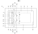
- FIG. 8 is a plan view of a substrate 1F according to the second embodiment.
- the mounting surface 2a of the insulating substrate 2 of the substrate 1F may be rectangular in plan view, having sides 2g and 2h that are parallel and opposed to each other, and sides 2i and 2j that are parallel and opposed to each other.
- the recesses 2b may be a pair of recesses 2b located along one side 2g of the mounting surface 2a.
- the substrate 1F has a pair of connection electrodes 3F corresponding to each of the pair of recesses 2b.
- Each of the pair of connection electrodes 3F has an underlying metallization layer 4F and a plating layer 5F.
- Each of the pair of underlying metallization layers 4F includes a bottom surface portion 4a, a wall surface portion 4b, and a mounting surface portion 4c.
- a width W1 along a width direction parallel to the side 2g of the mounting surface portion 4c of the underlying metallization layer 4F may be narrower than a width W2 along the above-mentioned width direction of the bottom surface portion 4a of the underlying metallization layer 4F.
- the mounting surface portion 4c of the base metallization layer 4F located in one of the pair of recesses 2b may be located closer to the other recess 2b in the width direction.
- FIG. 8 shows an example in which the mounting surface portion 4c and the plating layer 5d protrude, or the plating layer 5E protrudes, as in the examples shown in FIG. 6 and FIG. 7, to form a space.
- the convex portion 2k and the convex portion 2m as in the examples shown in FIG. 4 and FIG.
- the convex portion 2k, the mounting surface portion 4c, and the plating layer 5b protrude from the mounting surface 2a, or the convex portion 2m, the mounting surface portion 4c, and the plating layer 5c protrude from the mounting surface 2a, to form a space.
- the mounting surface portion 4c and the recessed portion 2b are generally rectangular (approximately oblong) in plan view, but the present disclosure is not limited to this, and the shape may be a part of a triangle, circle, ellipse, etc.
- the conductive bonding material 7 located above the bottom surface portion 4a of the base metallization layer 4F can move into the space and accumulate in this space.
- the space in which the conductive bonding material 17 can accumulate is called the accumulation region 2r.
- the conductive bonding material 7 can move to the accumulation region 2r.
- the piezoelectric vibration element 6 is bonded to the connection electrode 3F in the recess 2b, and is also bonded to the connection electrode 3F in the accumulation region 2r. Since the width of the mounting surface portion 4c is narrow, the accumulation region 2r is located within the width of the bottom surface portion 4a of the base metallization layer 4F in the recess 2b. Therefore, the conductive bonding material 7 is unlikely to spread beyond the width of the bottom surface portion 4a. Therefore, the risk of a short circuit between the conductive bonding materials 7 corresponding to each of a pair of connection electrodes 3F can be reduced.
- the conductive bonding material 7 is a conductive adhesive
- the surface roughness of the reservoir region 2r is greater than that of the plating layer, resulting in greater adhesive strength.
- the portion adjacent to the bottom surface portion 4a where the conductive bonding material 7 is located becomes the accumulation region 2r in which the conductive bonding material 7 can move, but the accumulation region 2r itself is in a position where the conductive bonding material 7 extends beyond the width of the bottom surface portion 4a.
- the mounting surface portion 4c is located closer to the other recess 2b, so the pooling region 2r is located away from the other recess 2b. Therefore, the distance between the pair of pooling regions 2r between the pair of connection electrodes 3F becomes larger. This makes it easier for the pair of conductive bonding materials 7 to spread and flow in opposite directions, reducing the possibility of the pair of conductive bonding materials 7 shorting out.
- the accumulation region 2r may be part of the recess 2b. In this case, the conductive bonding material 7 can move even more easily to the accumulation region 2r.
- FIG. 9 is a plan view of a substrate 1G according to a modified example.
- FIG. 10 is a cross-sectional view taken along line X-X shown in FIG. 9.
- the mounting surface 2a of the insulating substrate 2 of the substrate 1G may be rectangular in plan view, with sides 2g and 2h facing parallel to each other and sides 2i and 2j facing parallel to each other.
- the recesses 2b may be a pair of recesses 2b located at diagonally opposing corners of the mounting surface 2a.
- the wall surface 2d of the recesses 2b is located inside the mounting surface 2a of the recesses 2b.
- the recess 2b may be a pair of recesses 2b, one located near the edge 2g of the mounting surface 2a and the other located near the edge 2h opposite the edge 2g.
- the substrate 1G may be used as a double-supported substrate that supports the piezoelectric vibration element 6 at both ends.
- the recess 2b located near the side 2g may be located near the side 2i, and the recess 2b located near the side 2h may be located near the side 2j, which is the opposite side to the side 2i.
- the recess 2b may be a pair of recesses 2b located at corners facing each other along a diagonal line of the mounting surface 2a.
- the wall surface 2d of the recess 2b is located inside the mounting surface 2a of the recess 2b.
- the wall surface 2d formed in the recess 2b located near the side 2g may be the wall surface located on the opposite side of the recess 2b to the side 2g and farther from the side 2g.
- the wall surface 2d formed in the recess 2b located near the side 2h may be the wall surface located on the opposite side of the recess 2b to the side 2h and farther from the side 2h.
- the substrate 1G has a pair of connection electrodes 3 corresponding to each of the pair of recesses 2b. This allows the substrate 1G to be used for a piezoelectric vibration element 6 having terminals along a diagonal line.
- Each of the pair of connection electrodes 3 has a configuration similar to that shown in FIG. 1, and includes an underlying metallization layer 4 and a plating layer 5.
- Each of the pair of underlying metallization layers 4 includes a bottom surface portion 4a and a wall surface portion 4b.
- each plating layer 5 covering the exposed surface of the base metallization layer 4 extending along the wall surface 2d of a pair of recesses 2b located at diagonally opposing corners of the mounting surface 2a forms a bump of fine height, so that the pair of bumps is located in each recess 2b. This allows the position of the pair of bumps to be lowered. Therefore, the piezoelectric vibration element 6 to be connected can be mounted at a low position.
- the wall surface 2d of the recess 2b is the wall surface along which the wall surface portion 4b of the underlying metallization layer 4 extends.
- a bump (wall surface portion 4b) is formed on the inside of the recess 2b, and the conductive bonding material 7 is located on the outside of this bump. Therefore, the conductive bonding material 7 that attempts to flow into the gap between the mounting surface 2a and the piezoelectric vibration element 6 is blocked by the bump. As a result, the conductive bonding material 7 does not adhere to the vibrating portion of the piezoelectric vibration element 6, reducing the risk that the conductive bonding material 7 will affect the vibration of the piezoelectric vibration element 6.
- the plating layer 5 covering the exposed surface of the base metallization layer 4 forms a bump of fine height.
- This bump of fine height forms a space between the plating layer 5 located on the bottom surface portion 4a of the base metallization layer 4 and the piezoelectric vibration element 6, and the conductive bonding material 7 can be held in this space. Since the bump is located inside the mounting surface 2a with respect to the conductive bonding material 7, the risk of the conductive bonding material 7 spreading to the vibrating portion of the piezoelectric vibration element 6 is reduced, and the risk of the conductive bonding material 7 affecting the vibration of the piezoelectric vibration element 6 is reduced. In addition, the risk of the conductive bonding material 7 being held and crushed between the plating layer 5 and the piezoelectric vibration element 6 creeping up the side of the frame portion 2f is reduced.
- FIG. 11 is a plan view of substrate 1H according to another modified example.
- the mounting surface 2a of the insulating substrate 2 of the substrate 1H may be rectangular in plan view, with sides 2g and 2h facing parallel to each other and sides 2i and 2j facing parallel to each other.
- the recesses 2b may be a pair of recesses 2b located at diagonally opposing corners of the mounting surface 2a.
- the substrate 1H has a pair of connection electrodes 3F corresponding to each of the pair of recesses 2b.
- Each of the pair of connection electrodes 3F has an underlying metallization layer 4F and a plating layer 5F.
- Each of the pair of underlying metallization layers 4F includes a bottom surface portion 4a, a wall surface portion 4b, and a mounting surface portion 4c.
- a width W3 along a width direction parallel to the side 2g of the mounting surface portion 4c of the underlying metallization layer 4F may be narrower than a width W4 along the above-mentioned width direction of the bottom surface portion 4a of the underlying metallization layer 4F.
- the mounting surface portion 4c of the base metallization layer 4F located in one of the pair of recesses 2b may be located closer to the other recess 2b in the width direction.
- the mounting surface portion 4c is located closer to the other recess 2b, so the pooling region 2r is located away from the other recess 2b.
- the distance between the pair of pooling regions 2r between the pair of connection electrodes 3F becomes larger. This makes it easier for the pair of conductive bonding materials 7 to spread and flow in opposite directions, reducing the possibility of the pair of conductive bonding materials 7 shorting out even if the board is made smaller and the distance between the pair of connection electrodes 3F is shortened.
- the conductive bonding material 7 does not flow over the plating layer 5F but flows to the outer pooling region 2r, reducing the risk that the conductive bonding material 7 will affect the vibration of the piezoelectric vibration element 6.
- the conductive bonding material 7 that flows outward remains in the pooling region 2r and is unlikely to spread any further outward. This reduces the risk of a short circuit caused by the conductive bonding material 7 creeping up the inner wall of the frame portion 2f.
- FIG. 11 shows an example in which the mounting surface portion 4c and the plating layer 5d protrude, or the plating layer 5E protrudes, as in the examples shown in FIG. 6 and FIG. 7, to form a space.
- the convex portion 2k and the convex portion 2m as in the examples shown in FIG. 4 and FIG. 5, the convex portion 2k, the mounting surface portion 4c, and the plating layer 5b protrude, or the convex portion 2m, the mounting surface portion 4c, and the plating layer 5c protrude, to form a space.
- the conductive bonding material 7 located above the bottom surface 4a of the base metallization layer 4F can move to the accumulation region 2r. Because the width of the mounting surface portion 4c is narrow, the accumulation region 2r is located within the width of the bottom surface 4a of the base metallization layer 4F in the recess 2b. Therefore, the conductive bonding material 7 tends to spread toward the accumulation region 2r and is unlikely to spread beyond the width of the bottom surface 4a. Therefore, even if the board is miniaturized and the distance between a pair of connection electrodes 3H is shortened, the risk of a short circuit between the conductive bonding materials 7 corresponding to each of the pair of connection electrodes 3F can be reduced.
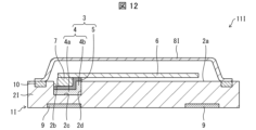
- FIG. 12 is a cross-sectional view of a piezoelectric device 11I according to the third embodiment.
- the piezoelectric device 11I comprises a substrate 1I, a piezoelectric vibration element 6 connected to the substrate 1I via a conductive bonding material 7, and a cup-shaped lid 8I provided on the substrate 1I to cover the piezoelectric vibration element 6.
- the substrate 1I has a mounting surface 2a on which the piezoelectric vibration element 6 is mounted, a flat-plate type insulating substrate 2I having one or more recesses 2b opening into the mounting surface 2a, and a connection electrode 3 connected to the piezoelectric vibration element 6.
- the lid 8I is bonded to a frame-shaped metallization layer 10 embedded in the mounting surface 2a of the insulating substrate 2I. In this way, the package structure of the piezoelectric device 11I provided with the substrate 1I may be of a flat-plate type.
- This configuration simplifies the structure compared to the first and second embodiments, making it possible to reduce costs. In addition, the risk of cracks occurring due to heat during sealing is reduced.
- FIG. 13 is a cross-sectional view of a modified piezoelectric device 11J.
- the piezoelectric device 11J includes a substrate 1J, a piezoelectric vibration element 6 connected to the substrate 1J via a conductive bonding material 7, and a flat cover 8 provided on the substrate 1J to cover the piezoelectric vibration element 6.
- the substrate 1J includes an H-shaped insulating substrate 2J having a mounting surface 2a on which the piezoelectric vibration element 6 is mounted, and one or more recesses 2b opening on the mounting surface 2a, and a connection electrode 3 connected to the piezoelectric vibration element 6.
- the insulating substrate 2J includes a flat base 2e, a frame 2f located on the upper surface of the base 2e, and a frame 2f located on the lower surface of the base 2e.
- the mounting surface 2a is an area surrounded by the frame 2f on the upper surface of the insulating substrate 2J, and corresponds to the bottom surface of the recess formed by the frame 2f.
- a recess is also formed on the lower surface of the insulating substrate 2J by the frame 2f.
- the insulating substrate 2J has an H-shaped cross section. In this way, the package structure of the piezoelectric device 11J including the substrate 1J may be an H-type.
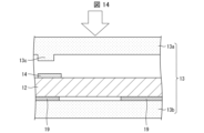
- Fig. 14 and Fig. 15 are cross-sectional views showing a method for manufacturing a substrate.
- Fig. 14 and Fig. 15 show a pressurizing step in the method for manufacturing a substrate, with Fig. 14 showing the state before pressurization and Fig. 15 showing the state after pressurization (during pressurization).
- Fig. 14 and Fig. 15 show only the main parts in the method for manufacturing the substrate 1E shown in Fig. 7.
- the method for manufacturing the substrate 1E involves first applying a metallization paste corresponding to the base metallization layer 4E as a base metallization pattern layer 14 to the upper surface of the ceramic green sheet 12 that will become the insulating substrate 2.
- the metallization paste is applied, for example, by screen printing.
- a metallization paste corresponding to the external electrode 9 is applied to the lower surface side of the ceramic green sheet 12 as an external electrode pattern 19.
- the ceramic green sheet 12 is an example of an insulating material according to the present disclosure.
- the frame-shaped metallization pattern corresponding to the frame-shaped metallization layer 10 can also be formed in the same manner as the base metallization pattern layer 14 and the external electrode pattern 19.
- the ceramic green sheet 12 with the metallization paste applied on both sides is pressed by a die 13 having projections and recesses corresponding to the projections and recesses of the base metallization layer 4E of the substrate 1E.
- a part of the base metallization pattern layer 14 located on the upper surface of the ceramic green sheet 12 is pressed by the projections 13c of the upper die 13a, and the entire base metallization pattern layer 14 is pressed into the interior of the ceramic green sheet 12.
- a recess 12b is formed on the upper surface of the ceramic green sheet 12.
- the external electrode pattern 19 located on the back surface of the ceramic green sheet 12 is pressed into the interior of the ceramic green sheet 12 pressed by the flat lower die 13b.
- the frame-shaped metallization pattern is also pressed into the surface of the ceramic green sheet 12.
- an insulating material (ceramic green sheet) 12 having an upper surface 12a that becomes the mounting surface 2a, one or more recesses 12b opening on the upper surface 12a, and an underlying metallization pattern 14E that extends along the bottom surface 12c of the recess 12b and extends along at least a part of the wall surface 12d of the recess 12b to reach the upper surface 12a are formed.
- the underlying metallization pattern 14E has a bottom surface portion 14a that extends along the bottom surface 12c of the recess 12b, a wall surface portion 14b that extends from the bottom surface portion 14a along the wall surface 12d of the recess 12b, and a mounting surface portion 14c that extends from the wall surface portion 14b along a direction parallel to the upper surface 12a.
- the recess 12b has a middle step portion 12p located between the bottom surface 12c and the upper surface 12a.
- the mounting surface portion 14c is located on the middle step portion 12p.
- the upper surface of the mounting surface portion 14c is on the same plane as the upper surface 12a.
- the ceramic green sheet 12 on which the recesses 12b and the base metallization pattern 14E are formed is subjected to a firing process to form an insulating substrate 2 having a mounting surface 2a on which the piezoelectric vibration element 6 is mounted, and one or more recesses 2b opening on the mounting surface 2a.
- a base metallization layer 4E is formed, which extends along the bottom surface 2c of the recesses 2b of the insulating substrate 2 and extends along at least a portion of the wall surface 2d of the recesses 2b to reach the mounting surface 2a.
- a plating process is performed on the insulating substrate 2 with the base metallization layer 4E to form a plating layer 5E that covers the exposed surface of the base metallization layer 4E.
- the firing process also forms the external electrode 9 and the frame-shaped metallization layer 10 at the same time, and in the plating layer formation process, a plating layer is also formed on the exposed surfaces of the external electrode 9 and the frame-shaped metallization layer 10.
- the above-described manufacturing method increases the density of the insulating substrate 2 and the underlying metallization layer 4E, thereby improving the package strength of the piezoelectric device 11.
- the manufacturing method of the substrate 1E according to this embodiment ensures the package strength even when the device is made thinner.
- the underlying metallization layer 4E is an area that becomes the bonding surface when the conductive bonding material 7 is applied or soldered, so it is effective in improving the package strength.
- the recess 2b and the base metallization layer 4E are formed by pressure processing using the mold 13, so they have high dimensional accuracy and high shape stability. Therefore, the plating layer 5E covering the exposed surface of the base metallization layer 4E also has high dimensional accuracy and high shape stability.
- the top surface of the bump composed of the plating layer 5E covering the base metallization layer 4E can be made relatively flat. Unlike the conventional configuration in which the base metallization layer is formed by printing and coating, the top surface of the bump does not become rounded like a semi-cylindrical stick. Therefore, the mounting stability of the piezoelectric vibration element 6 can be improved.
- a substrate 1E with stable dimensional accuracy in the height direction of the bump can be provided.
- the recess 2b and the base metallization layers 4, 4A to 4D of the substrate 1 shown in Figures 1 and 2 and the substrate 1A shown in Figure 3 to the substrate 1D shown in Figure 6 other than the substrate 1E can also be formed by using a mold 13 having concaves and convexes corresponding to the respective concaves and convexes.
- the bottom surface 4a and the recess 2b are the same size in a plan view, but the bottom surface 4a may be smaller than the bottom surface 2c of the recess 2b in a plan view.
- the bottom surface 2c of the recess 2b may be exposed around the bottom surface 4a. In this case, the bonding strength of the conductive adhesive is increased.
- the insulating substrate 2 may be formed by laminating or printing a plurality of ceramic green sheets and a metallization paste that will become a base metallization layer, firing them, and then plating them to achieve the substrate configuration described above in the first to third embodiments.
- the frame portion 2f of the insulating substrate 2 may be formed by laminating a frame-shaped ceramic green sheet on the ceramic green sheet, or by pressure forming using an upper mold 13a having a recess corresponding to the frame portion 2f.
- a so-called multi-piece substrate may be produced in which a plurality of substrates are arranged in a matrix, and the multi-piece substrate may be divided to obtain individual substrates.
- the substrate in aspect 1 of the present disclosure comprises an insulating substrate having a mounting surface on which a connection object is mounted and one or more recesses opening into the mounting surface, a connection electrode connected to the connection object, and the connection electrode has an underlying metallization layer that extends along the bottom surface of the recess and also extends along at least a portion of the wall surface of the recess to reach the mounting surface, and a plating layer that covers the exposed surface of the underlying metallization layer.
- the substrate in aspect 2 of the present disclosure is the substrate in aspect 1 above, in which the underlying metallization layer has a bottom surface portion that extends along the bottom surface of the recess, and a wall surface portion that extends from the bottom surface portion along the wall surface of the recess.
- the substrate in aspect 3 of the present disclosure is the substrate in aspect 2 above, further comprising a mounting surface portion in which the underlying metallization layer extends from the wall portion in a direction parallel to the mounting surface.
- the wall portion extends along the wall surface of the recess to a position on the same plane as the mounting surface.
- the substrate in aspect 5 of the present disclosure is the substrate in any one of aspects 2 to 4 above, in which the wall portion extends along the wall surface of the recess to a position protruding from the mounting surface.
- the substrate in aspect 6 of the present disclosure is the substrate in aspect 3 above, further comprising a mounting surface portion in which the base metallization layer extends from the wall portion in a direction parallel to the mounting surface.
- the substrate in aspect 7 of the present disclosure is the substrate in aspect 3 or 6 above, in which the recess has a middle stage portion located between the bottom surface and the mounting surface, and the mounting surface portion is located above the middle stage portion.
- the substrate in aspect 8 of the present disclosure is the substrate in aspect 3, 6, or 7 above, in which the mounting surface portion extends above the mounting surface.
- the substrate in aspect 9 of the present disclosure is the substrate in any one of aspects 1 to 8 above, in which the mounting surface is rectangular in plan view, the one or more recesses are a pair of recesses located along one side of the mounting surface, and the wall surface of the recess is a wall surface located on the opposite side to the one side of the mounting surface of the recess.
- the substrate in aspect 10 of the present disclosure is the substrate in any one of aspects 3 or 6 to 8 above, in which the mounting surface is rectangular in plan view, the one or more recesses are a pair of recesses located along one side of the mounting surface, and the width of the mounting surface portion of the underlying metallization layer along a width direction parallel to the one side is narrower than the width of the bottom surface portion of the underlying metallization layer along the width direction.
- the substrate in aspect 11 of the present disclosure is the substrate in aspect 10 above, in which the mounting surface portion of the base metallization layer located in one of the pair of recesses is located closer to the other of the pair of recesses in the width direction.
- the substrate in aspect 12 of the present disclosure is the substrate in any one of aspects 1 to 11 above, in which the mounting surface is rectangular in plan view, the one or more recesses are a pair of recesses located at diagonally opposing corners of the mounting surface, and the wall surface of the recess is a wall surface located inside the mounting surface of the recess.
- the substrate in aspect 13 of the present disclosure is the substrate in any one of aspects 3, 6 to 8, or 10 to 11 above, in which the mounting surface is rectangular in plan view, the one or more recesses are a pair of recesses located at corners facing each other along a diagonal of the mounting surface, and the width of the mounting surface portion of the underlying metallization layer along a width direction parallel to one side of the mounting surface is narrower than the width of the bottom surface portion of the underlying metallization layer along the width direction.
- the substrate in aspect 14 of the present disclosure is the substrate in aspect 13 above, in which the mounting surface portion of the base metallization layer located in one of the pair of recesses is located closer to the other of the pair of recesses in the width direction.
- the electronic device includes a substrate according to any one of aspects 1 to 14 above, a piezoelectric vibration element connected to the substrate via a conductive bonding material, and a lid provided on the substrate so as to cover the piezoelectric vibration element.
- the method of manufacturing a substrate in aspect 16 of the present disclosure includes a pressurizing step of pressing an insulating material having a base metallization pattern on its surface with a mold to form an insulating substrate having a mounting surface on which a connection target is mounted and one or more recesses opening into the mounting surface, and a base metallization layer that extends along the bottom surface of the recess and also extends along at least a portion of the wall surface of the recess to reach the mounting surface, and a plating layer formation step of forming a plating layer that covers the exposed surface of the base metallization layer.
Landscapes
- Engineering & Computer Science (AREA)
- Manufacturing & Machinery (AREA)
- Physics & Mathematics (AREA)
- Acoustics & Sound (AREA)
- Piezo-Electric Or Mechanical Vibrators, Or Delay Or Filter Circuits (AREA)
- Electric Connection Of Electric Components To Printed Circuits (AREA)
- Printing Elements For Providing Electric Connections Between Printed Circuits (AREA)
- Structure Of Printed Boards (AREA)
Priority Applications (1)
| Application Number | Priority Date | Filing Date | Title |
|---|---|---|---|
| JP2025503825A JPWO2024181272A1 (https=) | 2023-02-28 | 2024-02-21 |
Applications Claiming Priority (2)
| Application Number | Priority Date | Filing Date | Title |
|---|---|---|---|
| JP2023030327 | 2023-02-28 | ||
| JP2023-030327 | 2023-02-28 |
Publications (1)
| Publication Number | Publication Date |
|---|---|
| WO2024181272A1 true WO2024181272A1 (ja) | 2024-09-06 |
Family
ID=92590608
Family Applications (1)
| Application Number | Title | Priority Date | Filing Date |
|---|---|---|---|
| PCT/JP2024/006299 Ceased WO2024181272A1 (ja) | 2023-02-28 | 2024-02-21 | 基板、電子装置、及び、基板の製造方法 |
Country Status (3)
| Country | Link |
|---|---|
| JP (1) | JPWO2024181272A1 (https=) |
| TW (1) | TW202439540A (https=) |
| WO (1) | WO2024181272A1 (https=) |
Citations (5)
| Publication number | Priority date | Publication date | Assignee | Title |
|---|---|---|---|---|
| JP2006237142A (ja) * | 2005-02-23 | 2006-09-07 | Sumitomo Metal Electronics Devices Inc | セラミック基板及びその製造方法 |
| JP2006332553A (ja) * | 2005-05-30 | 2006-12-07 | Fujifilm Holdings Corp | 配線基板製造方法及び吐出ヘッド並びに画像形成装置 |
| JP2009065149A (ja) * | 2008-08-27 | 2009-03-26 | Shinko Electric Ind Co Ltd | 配線基板 |
| JP2010226419A (ja) * | 2009-03-24 | 2010-10-07 | Seiko Epson Corp | 圧電デバイスおよびその製造方法 |
| WO2019146699A1 (ja) * | 2018-01-24 | 2019-08-01 | 京セラ株式会社 | 配線基板、電子装置及び電子モジュール |
-
2024
- 2024-02-21 WO PCT/JP2024/006299 patent/WO2024181272A1/ja not_active Ceased
- 2024-02-21 JP JP2025503825A patent/JPWO2024181272A1/ja active Pending
- 2024-02-23 TW TW113106660A patent/TW202439540A/zh unknown
Patent Citations (5)
| Publication number | Priority date | Publication date | Assignee | Title |
|---|---|---|---|---|
| JP2006237142A (ja) * | 2005-02-23 | 2006-09-07 | Sumitomo Metal Electronics Devices Inc | セラミック基板及びその製造方法 |
| JP2006332553A (ja) * | 2005-05-30 | 2006-12-07 | Fujifilm Holdings Corp | 配線基板製造方法及び吐出ヘッド並びに画像形成装置 |
| JP2009065149A (ja) * | 2008-08-27 | 2009-03-26 | Shinko Electric Ind Co Ltd | 配線基板 |
| JP2010226419A (ja) * | 2009-03-24 | 2010-10-07 | Seiko Epson Corp | 圧電デバイスおよびその製造方法 |
| WO2019146699A1 (ja) * | 2018-01-24 | 2019-08-01 | 京セラ株式会社 | 配線基板、電子装置及び電子モジュール |
Also Published As
| Publication number | Publication date |
|---|---|
| TW202439540A (zh) | 2024-10-01 |
| JPWO2024181272A1 (https=) | 2024-09-06 |
Similar Documents
| Publication | Publication Date | Title |
|---|---|---|
| CN103180941B (zh) | 布线基板 | |
| JP2001196488A (ja) | 電子部品装置及びその製造方法 | |
| CN104335345A (zh) | 布线基板以及电子装置 | |
| US9704791B2 (en) | Wiring board and electronic device | |
| US7583162B2 (en) | Piezoelectric device and method for manufacturing the piezoelectric device | |
| CN104412722A (zh) | 布线基板、电子装置以及发光装置 | |
| JP5101201B2 (ja) | 圧電発振器 | |
| CN111512432B (zh) | 布线基板、电子装置以及电子模块 | |
| WO2019044706A1 (ja) | 電子部品搭載用基板、電子装置および電子モジュール | |
| JP7069222B2 (ja) | 配線基板、電子装置及び電子モジュール | |
| WO2024181272A1 (ja) | 基板、電子装置、及び、基板の製造方法 | |
| JP2008131167A (ja) | 圧電デバイスのパッケージ構造及び圧電デバイス | |
| JP2005243739A (ja) | 電子部品収納用パッケージおよび電子装置 | |
| WO2019017441A1 (ja) | 電子部品収納用パッケージ、電子装置および電子モジュール | |
| JP6129491B2 (ja) | 多数個取り配線基板 | |
| JP7784565B2 (ja) | 配線基板、電子装置、及び電子モジュール | |
| JP2005079656A (ja) | 圧電振動子 | |
| JP5004837B2 (ja) | 構造体及び電子装置 | |
| JP2006066648A (ja) | 多数個取り配線基板、電子部品収納用パッケージおよび電子装置 | |
| JPWO2024070528A5 (https=) | ||
| JP2005244146A (ja) | 電子部品収納用パッケージおよび電子装置ならびに電子装置の実装構造 | |
| JP2006278756A (ja) | 圧電振動子収納用パッケージおよび圧電装置 | |
| WO2025047324A1 (ja) | 配線基板、パッケージ、および圧電デバイス | |
| JP3810335B2 (ja) | 配線基板 | |
| JP4904846B2 (ja) | 圧電発振器、収容器、および収容器の製造方法 |
Legal Events
| Date | Code | Title | Description |
|---|---|---|---|
| 121 | Ep: the epo has been informed by wipo that ep was designated in this application |
Ref document number: 24763753 Country of ref document: EP Kind code of ref document: A1 |
|
| ENP | Entry into the national phase |
Ref document number: 2025503825 Country of ref document: JP Kind code of ref document: A |
|
| WWE | Wipo information: entry into national phase |
Ref document number: 2025503825 Country of ref document: JP |
|
| NENP | Non-entry into the national phase |
Ref country code: DE |
|
| 122 | Ep: pct application non-entry in european phase |
Ref document number: 24763753 Country of ref document: EP Kind code of ref document: A1 |