WO2024166181A1 - サセプタ - Google Patents
サセプタ Download PDFInfo
- Publication number
- WO2024166181A1 WO2024166181A1 PCT/JP2023/003830 JP2023003830W WO2024166181A1 WO 2024166181 A1 WO2024166181 A1 WO 2024166181A1 JP 2023003830 W JP2023003830 W JP 2023003830W WO 2024166181 A1 WO2024166181 A1 WO 2024166181A1
- Authority
- WO
- WIPO (PCT)
- Prior art keywords
- ceramic
- gas supply
- supply hole
- susceptor
- ceramic plate
- Prior art date
- Legal status (The legal status is an assumption and is not a legal conclusion. Google has not performed a legal analysis and makes no representation as to the accuracy of the status listed.)
- Ceased
Links
Images



Classifications
-
- H—ELECTRICITY
- H10—SEMICONDUCTOR DEVICES; ELECTRIC SOLID-STATE DEVICES NOT OTHERWISE PROVIDED FOR
- H10P—GENERIC PROCESSES OR APPARATUS FOR THE MANUFACTURE OR TREATMENT OF DEVICES COVERED BY CLASS H10
- H10P72/00—Handling or holding of wafers, substrates or devices during manufacture or treatment thereof
- H10P72/70—Handling or holding of wafers, substrates or devices during manufacture or treatment thereof for supporting or gripping
- H10P72/72—Handling or holding of wafers, substrates or devices during manufacture or treatment thereof for supporting or gripping using electrostatic chucks
- H10P72/722—Details of electrostatic chucks
-
- H—ELECTRICITY
- H10—SEMICONDUCTOR DEVICES; ELECTRIC SOLID-STATE DEVICES NOT OTHERWISE PROVIDED FOR
- H10P—GENERIC PROCESSES OR APPARATUS FOR THE MANUFACTURE OR TREATMENT OF DEVICES COVERED BY CLASS H10
- H10P72/00—Handling or holding of wafers, substrates or devices during manufacture or treatment thereof
- H10P72/04—Apparatus for manufacture or treatment
- H10P72/0431—Apparatus for thermal treatment
- H10P72/0432—Apparatus for thermal treatment mainly by conduction
-
- C—CHEMISTRY; METALLURGY
- C23—COATING METALLIC MATERIAL; COATING MATERIAL WITH METALLIC MATERIAL; CHEMICAL SURFACE TREATMENT; DIFFUSION TREATMENT OF METALLIC MATERIAL; COATING BY VACUUM EVAPORATION, BY SPUTTERING, BY ION IMPLANTATION OR BY CHEMICAL VAPOUR DEPOSITION, IN GENERAL; INHIBITING CORROSION OF METALLIC MATERIAL OR INCRUSTATION IN GENERAL
- C23C—COATING METALLIC MATERIAL; COATING MATERIAL WITH METALLIC MATERIAL; SURFACE TREATMENT OF METALLIC MATERIAL BY DIFFUSION INTO THE SURFACE, BY CHEMICAL CONVERSION OR SUBSTITUTION; COATING BY VACUUM EVAPORATION, BY SPUTTERING, BY ION IMPLANTATION OR BY CHEMICAL VAPOUR DEPOSITION, IN GENERAL
- C23C14/00—Coating by vacuum evaporation, by sputtering or by ion implantation of the coating forming material
- C23C14/22—Coating by vacuum evaporation, by sputtering or by ion implantation of the coating forming material characterised by the process of coating
- C23C14/50—Substrate holders
-
- C—CHEMISTRY; METALLURGY
- C23—COATING METALLIC MATERIAL; COATING MATERIAL WITH METALLIC MATERIAL; CHEMICAL SURFACE TREATMENT; DIFFUSION TREATMENT OF METALLIC MATERIAL; COATING BY VACUUM EVAPORATION, BY SPUTTERING, BY ION IMPLANTATION OR BY CHEMICAL VAPOUR DEPOSITION, IN GENERAL; INHIBITING CORROSION OF METALLIC MATERIAL OR INCRUSTATION IN GENERAL
- C23C—COATING METALLIC MATERIAL; COATING MATERIAL WITH METALLIC MATERIAL; SURFACE TREATMENT OF METALLIC MATERIAL BY DIFFUSION INTO THE SURFACE, BY CHEMICAL CONVERSION OR SUBSTITUTION; COATING BY VACUUM EVAPORATION, BY SPUTTERING, BY ION IMPLANTATION OR BY CHEMICAL VAPOUR DEPOSITION, IN GENERAL
- C23C16/00—Chemical coating by decomposition of gaseous compounds, without leaving reaction products of surface material in the coating, i.e. chemical vapour deposition [CVD] processes
- C23C16/44—Chemical coating by decomposition of gaseous compounds, without leaving reaction products of surface material in the coating, i.e. chemical vapour deposition [CVD] processes characterised by the method of coating
- C23C16/458—Chemical coating by decomposition of gaseous compounds, without leaving reaction products of surface material in the coating, i.e. chemical vapour deposition [CVD] processes characterised by the method of coating characterised by the method used for supporting substrates in the reaction chamber
- C23C16/4582—Rigid and flat substrates, e.g. plates or discs
- C23C16/4583—Rigid and flat substrates, e.g. plates or discs the substrate being supported substantially horizontally
-
- H—ELECTRICITY
- H01—ELECTRIC ELEMENTS
- H01J—ELECTRIC DISCHARGE TUBES OR DISCHARGE LAMPS
- H01J37/00—Discharge tubes with provision for introducing objects or material to be exposed to the discharge, e.g. for the purpose of examination or processing thereof
- H01J37/32—Gas-filled discharge tubes
- H01J37/32431—Constructional details of the reactor
- H01J37/32715—Workpiece holder
-
- H—ELECTRICITY
- H10—SEMICONDUCTOR DEVICES; ELECTRIC SOLID-STATE DEVICES NOT OTHERWISE PROVIDED FOR
- H10P—GENERIC PROCESSES OR APPARATUS FOR THE MANUFACTURE OR TREATMENT OF DEVICES COVERED BY CLASS H10
- H10P72/00—Handling or holding of wafers, substrates or devices during manufacture or treatment thereof
- H10P72/04—Apparatus for manufacture or treatment
- H10P72/0402—Apparatus for fluid treatment
-
- H—ELECTRICITY
- H10—SEMICONDUCTOR DEVICES; ELECTRIC SOLID-STATE DEVICES NOT OTHERWISE PROVIDED FOR
- H10P—GENERIC PROCESSES OR APPARATUS FOR THE MANUFACTURE OR TREATMENT OF DEVICES COVERED BY CLASS H10
- H10P72/00—Handling or holding of wafers, substrates or devices during manufacture or treatment thereof
- H10P72/04—Apparatus for manufacture or treatment
- H10P72/0431—Apparatus for thermal treatment
- H10P72/0434—Apparatus for thermal treatment mainly by convection
-
- H—ELECTRICITY
- H10—SEMICONDUCTOR DEVICES; ELECTRIC SOLID-STATE DEVICES NOT OTHERWISE PROVIDED FOR
- H10P—GENERIC PROCESSES OR APPARATUS FOR THE MANUFACTURE OR TREATMENT OF DEVICES COVERED BY CLASS H10
- H10P72/00—Handling or holding of wafers, substrates or devices during manufacture or treatment thereof
- H10P72/70—Handling or holding of wafers, substrates or devices during manufacture or treatment thereof for supporting or gripping
- H10P72/72—Handling or holding of wafers, substrates or devices during manufacture or treatment thereof for supporting or gripping using electrostatic chucks
-
- H—ELECTRICITY
- H10—SEMICONDUCTOR DEVICES; ELECTRIC SOLID-STATE DEVICES NOT OTHERWISE PROVIDED FOR
- H10P—GENERIC PROCESSES OR APPARATUS FOR THE MANUFACTURE OR TREATMENT OF DEVICES COVERED BY CLASS H10
- H10P72/00—Handling or holding of wafers, substrates or devices during manufacture or treatment thereof
- H10P72/70—Handling or holding of wafers, substrates or devices during manufacture or treatment thereof for supporting or gripping
- H10P72/76—Handling or holding of wafers, substrates or devices during manufacture or treatment thereof for supporting or gripping using mechanical means, e.g. clamps or pinches
- H10P72/7604—Handling or holding of wafers, substrates or devices during manufacture or treatment thereof for supporting or gripping using mechanical means, e.g. clamps or pinches the wafers being placed on a susceptor, stage or support
- H10P72/7614—Handling or holding of wafers, substrates or devices during manufacture or treatment thereof for supporting or gripping using mechanical means, e.g. clamps or pinches the wafers being placed on a susceptor, stage or support characterised by a plurality of individual support members, e.g. support posts or protrusions
-
- H—ELECTRICITY
- H10—SEMICONDUCTOR DEVICES; ELECTRIC SOLID-STATE DEVICES NOT OTHERWISE PROVIDED FOR
- H10P—GENERIC PROCESSES OR APPARATUS FOR THE MANUFACTURE OR TREATMENT OF DEVICES COVERED BY CLASS H10
- H10P72/00—Handling or holding of wafers, substrates or devices during manufacture or treatment thereof
- H10P72/70—Handling or holding of wafers, substrates or devices during manufacture or treatment thereof for supporting or gripping
- H10P72/76—Handling or holding of wafers, substrates or devices during manufacture or treatment thereof for supporting or gripping using mechanical means, e.g. clamps or pinches
- H10P72/7604—Handling or holding of wafers, substrates or devices during manufacture or treatment thereof for supporting or gripping using mechanical means, e.g. clamps or pinches the wafers being placed on a susceptor, stage or support
- H10P72/7616—Handling or holding of wafers, substrates or devices during manufacture or treatment thereof for supporting or gripping using mechanical means, e.g. clamps or pinches the wafers being placed on a susceptor, stage or support characterised by a coating, a hardness or a material
-
- H—ELECTRICITY
- H10—SEMICONDUCTOR DEVICES; ELECTRIC SOLID-STATE DEVICES NOT OTHERWISE PROVIDED FOR
- H10P—GENERIC PROCESSES OR APPARATUS FOR THE MANUFACTURE OR TREATMENT OF DEVICES COVERED BY CLASS H10
- H10P72/00—Handling or holding of wafers, substrates or devices during manufacture or treatment thereof
- H10P72/70—Handling or holding of wafers, substrates or devices during manufacture or treatment thereof for supporting or gripping
- H10P72/76—Handling or holding of wafers, substrates or devices during manufacture or treatment thereof for supporting or gripping using mechanical means, e.g. clamps or pinches
- H10P72/7604—Handling or holding of wafers, substrates or devices during manufacture or treatment thereof for supporting or gripping using mechanical means, e.g. clamps or pinches the wafers being placed on a susceptor, stage or support
- H10P72/7624—Handling or holding of wafers, substrates or devices during manufacture or treatment thereof for supporting or gripping using mechanical means, e.g. clamps or pinches the wafers being placed on a susceptor, stage or support characterised by the mechanical construction of the susceptor, stage or support
-
- H—ELECTRICITY
- H10—SEMICONDUCTOR DEVICES; ELECTRIC SOLID-STATE DEVICES NOT OTHERWISE PROVIDED FOR
- H10P—GENERIC PROCESSES OR APPARATUS FOR THE MANUFACTURE OR TREATMENT OF DEVICES COVERED BY CLASS H10
- H10P72/00—Handling or holding of wafers, substrates or devices during manufacture or treatment thereof
- H10P72/70—Handling or holding of wafers, substrates or devices during manufacture or treatment thereof for supporting or gripping
- H10P72/76—Handling or holding of wafers, substrates or devices during manufacture or treatment thereof for supporting or gripping using mechanical means, e.g. clamps or pinches
- H10P72/7604—Handling or holding of wafers, substrates or devices during manufacture or treatment thereof for supporting or gripping using mechanical means, e.g. clamps or pinches the wafers being placed on a susceptor, stage or support
- H10P72/7626—Handling or holding of wafers, substrates or devices during manufacture or treatment thereof for supporting or gripping using mechanical means, e.g. clamps or pinches the wafers being placed on a susceptor, stage or support characterised by the construction of the shaft
Definitions
- the present invention relates to a susceptor for a film forming apparatus or an etching apparatus.
- susceptors are used to support wafers.
- a widely used susceptor is one that has a ceramic plate on which the wafer is placed and a cylindrical ceramic shaft attached to the ceramic plate.
- Patent Document 1 discloses an electrostatic chuck heater that includes a disk-shaped ceramic base with an electrostatic electrode and a resistance heating element, a hollow shaft, a convex ring, and a through hole.
- This electrostatic chuck heater is provided with a through hole that penetrates from the lower end of the peripheral wall of the hollow shaft to a predetermined position on the surface of the ceramic base, thereby making it possible to supply gas from the lower end of the hollow shaft to the space below the wafer surrounded by the ceramic base, the convex ring, and the wafer.
- Supplying gas to the space below the wafer makes it difficult for components that will become a conductive film to enter the gap between the convex ring and the wafer, and makes it difficult for an undesirable conductive film to adhere to the upper surface of the convex ring.
- Patent Document 2 JP 2020-072262 A discloses an electrostatic chuck that includes a ceramic dielectric substrate, a base plate that supports the ceramic dielectric substrate and has a gas introduction path, and a porous portion that is provided between the base plate and the ceramic dielectric substrate and faces the gas introduction path.
- the gas supply hole 116 is configured as a through hole that reaches from the distal end 114a (the end that is assembled to the device) of the ceramic shaft 114 to the surface 112a of the ceramic plate 112.
- the distal end 114a of the ceramic shaft 114 is assembled to a metal part 122 that constitutes the device, abnormal discharge may occur due to insufficient insulation distance between the metal part 122 and the ceramic plate surface 112a exposed to the plasma.
- the inventors have now discovered that in a susceptor having gas supply holes penetrating the shaft and plate, embedding a porous plug in a specified position in the gas supply hole can suppress the occurrence of arcing in a high-power plasma environment.
- the object of the present invention is therefore to provide a susceptor that has gas supply holes penetrating the shaft and plate, yet can suppress the occurrence of arcing in a high-power plasma environment.
- a susceptor for a film forming apparatus or an etching apparatus a ceramic plate having a first surface on which a wafer is placed and a second surface opposite to the first surface, and having an internal electrode embedded therein; a cylindrical ceramic shaft attached to the second surface of the ceramic plate; a gas supply hole extending through the ceramic plate and the ceramic shaft from the first surface of the ceramic plate through the second surface of the ceramic plate to a distal end of the ceramic shaft remote from the ceramic plate; a porous plug embedded in at least a portion of the gas supply hole corresponding to the ceramic plate;
- a susceptor comprising: [Aspect 2] 2.
- the susceptor of claim 1 further comprising a cooling jacket secured to the distal end, the cooling jacket having through holes in communication with the gas supply holes.
- a ceramic protective tube forming an inner wall of the gas supply hole in a region between the lower end and the distal end of the porous plug.
- the protective tube is made of alumina.
- the elastic member is a spring.
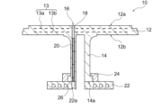
- FIG. 1 is a schematic cross-sectional view showing an example of a susceptor according to the present invention.
- FIG. 2 is a schematic top view of the susceptor shown in FIG.
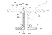
- FIG. 4 is a schematic cross-sectional view showing another example of a susceptor according to the present invention.
- FIG. 4 is a schematic cross-sectional view showing another example of a susceptor according to the present invention.
- FIG. 1 is a schematic cross-sectional view showing an example of a conventional susceptor.
- the susceptor according to the present invention is a platform for supporting a wafer, used in a film formation apparatus or an etching apparatus, particularly a film formation apparatus or an etching apparatus for a semiconductor manufacturing process.
- the susceptor according to the present invention may be a ceramic heater for a semiconductor film formation apparatus, or an electrostatic chuck for a semiconductor etching apparatus.
- it may be an electrostatic chuck heater that combines a heater function and an electrostatic chuck function.
- film formation apparatus include CVD (chemical vapor deposition) apparatus (e.g., thermal CVD apparatus, plasma CVD apparatus, photo CVD apparatus, and MOCVD apparatus) and PVD (physical vapor deposition) apparatus.
- FIGS. 1 and 2 show an example of a susceptor.
- the susceptor 10 shown in FIGS. 1 and 2 comprises a ceramic plate 12, a cylindrical ceramic shaft 14, a gas supply hole 16, and a porous plug 18.
- An internal electrode 13 is embedded in the ceramic plate 12.
- the ceramic plate 12 has a first surface 12a on which a wafer (not shown) is placed and a second surface 12b opposite the first surface 12a, and a ceramic shaft 14 is attached to the second surface 12b.
- the gas supply hole 16 is configured to penetrate the ceramic plate 12 and the ceramic shaft 14 so as to extend from the first surface 12a of the ceramic plate 12 through the second surface 12b to the distal end 14a of the ceramic shaft 14 away from the ceramic plate 12.
- a porous plug 18 is embedded in at least the portion of the gas supply hole 16 that corresponds to the ceramic plate 12. In this way, in a susceptor 10 having gas supply holes 16 penetrating the ceramic shaft 14 and the ceramic plate 12, by embedding a porous plug 18 in a predetermined position of the gas supply hole 16, it is possible to suppress the occurrence of arcing in a high-power plasma environment.
- the insulation distance from the ceramic plate surface 112a to the distal end 114a of the ceramic shaft 114 is insufficient, and there is a concern that arcing may occur. That is, since the distal end 114a of the ceramic shaft 114 is attached to a metal part 122 constituting the device, abnormal discharge may occur due to an insufficient insulation distance between the metal part 122 and the ceramic plate surface 112a exposed to the plasma.
- the occurrence of arcing can be suppressed by embedding a porous plug 18 in at least the part of the gas supply hole 16 corresponding to the ceramic plate 12.
- the porous plug 18 closes the gas supply hole 16 in a breathable manner, and the length of the gas passage path can be extremely long. That is, the porous plug 18 has an open pore structure because it has porosity that allows air to pass through, but the length of the gas passage path provided by the open pore structure is naturally much longer than the length of the gas supply hole 16. Moreover, since the porous plug 18 is generally made of an insulating material such as ceramic, it has excellent insulation resistance and therefore can be said to have excellent arcing suppression effects. Therefore, it is possible to prevent arcing (abnormal discharge) that may occur due to insufficient insulation distance between the distal end 14a of the ceramic shaft 14 and the first surface 12a of the ceramic plate 12. In that sense, the length of the ceramic shaft 14 and the gas supply hole 16 themselves does not need to be changed from the existing ones, and therefore it can be said to be advantageous in that it can be used in existing film formation equipment and etching equipment without design changes.
- the ceramic plate 12 can be of the same configuration as ceramic plates used in known ceramic susceptors.
- the main portion of the ceramic plate 12 other than the internal electrode 13 i.e., the ceramic base
- the preferred shape of the ceramic plate 12 is a disk.
- the planar shape of the disk-shaped ceramic plate 12 does not have to be a perfect circle, and may be an incomplete circle with a portion missing, such as an orientation flat.
- the size of the ceramic plate 12 can be determined appropriately according to the diameter of the wafer for which it is intended to be used, and is not particularly limited, but if it is a circle, the diameter is typically 150 to 450 mm, for example about 300 mm.
- protrusions are provided on the first surface 12a of the ceramic plate 12.
- the protrusions are intended to contact the rear surface of the wafer to support the wafer and to ensure a flow path for gas (e.g., heat transfer gas) supplied from the gas supply holes 16, and are preferably arranged at equal intervals from each other on the first surface 12a of the ceramic plate 12.
- the shape of each protrusion is not particularly limited, but is preferably cylindrical.
- the diameter of each protrusion is not particularly limited, but is preferably 0.1 to 8 mm, more preferably 0.5 to 5 mm, even more preferably 0.5 to 4 mm, and particularly preferably 0.70 to 2.54 mm.
- the protrusions are integrally formed with the ceramic plate 12 by embossing or the like. Therefore, like the ceramic plate 12, the protrusions are preferably made of aluminum nitride.
- the height of the protrusions is not particularly limited, but is preferably 0.001 to 0.1 mm, more preferably 0.005 to 0.08 mm, even more preferably 0.01 to 0.05 mm, and particularly preferably 0.01 to 0.03 mm.
- the distance between the central axes of adjacent protrusions is preferably 4 to 30 mm, more preferably 5 to 26 mm, even more preferably 7 to 26 mm, and particularly preferably 7 to 15 mm.
- An internal electrode 13 is embedded in the ceramic plate 12.
- Preferred examples of the internal electrode 13 include an ESC electrode, a heater electrode, and an RF electrode.
- two types of internal electrodes 13a and 13b may be provided as shown in the illustrated example.
- the internal electrode 13a provided in the region close to the first surface 12a may be an ESC electrode.
- the ESC electrode is an abbreviation of electrostatic chuck (ESC) electrode, and is also called an electrostatic electrode.
- the ESC electrode is preferably a circular thin-layer electrode having a diameter slightly smaller than that of the ceramic plate 12, and may be, for example, a mesh-like electrode formed by weaving thin metal wires into a net shape into a sheet shape.
- the ESC electrode may be used as a plasma electrode. That is, by applying a high frequency to the ESC electrode, the ESC electrode can also be used as a plasma electrode, and film formation can also be performed by a plasma CVD process.
- An ESC rod (not shown) is connected to the ESC electrode for power supply, and the ESC rod is connected to an external power source (not shown) through the internal space of the ceramic shaft 14.
- the ESC electrode chucks a wafer placed on the first surface 12a.
- the chucking force at this time is a Johnsen-Rahbek force because the volume resistivity of aluminum nitride that may constitute the main portion of the ceramic plate 12 is 1 ⁇ 10 8 to 1 ⁇ 10 13 ⁇ cm.
- the internal electrode 13b provided in the region close to the second surface 12b may be a heater electrode.
- the heater electrode is not particularly limited, but may be, for example, a conductive coil wired in a single stroke across the entire surface of the ceramic plate 12.
- Heater rods (not shown) are connected to both ends of the heater electrode for power supply, and the heater rods are connected to a heater power supply (not shown) via the internal space of the ceramic shaft 14.
- the heater electrode When power is supplied from the heater power supply, the heater electrode generates heat and heats the wafer placed on the first surface 12a.
- the heater electrode is not limited to a coil, and may be, for example, a ribbon (a long, thin plate) or a mesh.
- the ceramic shaft 14 is a cylindrical shaft attached to the second surface 12b of the ceramic plate 12, and may have the same configuration as ceramic shafts used in known ceramic susceptors.
- the ceramic shaft 14 has an internal space for accommodating rods (not shown) such as an ESC rod or a heater rod.
- the ceramic shaft 14 is preferably made of the same ceramic material as the ceramic plate 12. Therefore, the ceramic shaft 14 is preferably made of aluminum nitride.
- the upper end surface of the ceramic shaft 14 is preferably joined to the second surface 12b of the ceramic plate 12 by solid-state bonding or diffusion bonding.
- the outer diameter of the ceramic shaft 14 is not particularly limited, and is, for example, about 40 mm.
- the inner diameter of the ceramic shaft 14 (diameter of the internal space) is also not particularly limited, and is, for example, about 36 mm.
- the gas supply hole 16 is a through hole configured to penetrate the ceramic plate 12 and the ceramic shaft 14 so as to extend from the first surface 12a of the ceramic plate 12 through the second surface 12b to the distal end 14a of the ceramic shaft 14.
- the presence of the gas supply hole 16 allows gas to be supplied to the first surface 12a of the ceramic plate 12.
- a wafer is placed on the first surface 12a, and by supplying gas to the back surface of the wafer, heat generated in the ceramic plate 12 (particularly the heater electrode) can be efficiently transferred to the wafer. Therefore, the gas supplied to the gas supply hole 16 is preferably an inert gas with excellent heat conductivity, and He gas is particularly preferred.
- the planar shape of the gas supply holes 16 may be any shape, such as circular or polygonal, but is preferably circular.
- the number of gas supply holes 16 provided in the ceramic plate 12 is preferably 1 to 10, more preferably 2 to 6, and even more preferably 4. Within this range, gas can be supplied sufficiently while ensuring a large effective area in the ceramic plate 12.
- the diameter of the gas supply holes 16 is not particularly limited, but is preferably 0.5 to 4.0 mm, more preferably 0.5 to 2.0 mm, and even more preferably 0.9 to 1.1 mm.
- the porous plug 18 is embedded in at least the portion of the gas supply hole 16 that corresponds to the ceramic plate 12.
- the porous plug 18 is not particularly limited as long as it is a member or part that includes a porous material having gas permeability, but such a porous material is preferably composed of an insulating material such as ceramic in order to effectively suppress the occurrence of arcing. For example, it is made of alumina.
- a porous plug is attached to the tuyere refractory of the bottom wall of a molten metal container such as a ladle or tundish, and is known as a porous refractory having gas permeability for blowing gas into the molten metal, and such a commercially available porous plug can be used.
- porous ceramic member called a porous plug or ceramic plug and used in the gas introduction path of a susceptor such as an electrostatic chuck can also be used as the porous plug 18.
- the diameter of the porous plug 18 is not particularly limited as long as it can block the gas supply hole 16.
- a porous plug 18 with a diameter that matches the diameter of the gas supply hole 16 may be selected, or the diameter of the gas supply hole 16 may be set to match the diameter of the porous plug 18 to be adopted.
- the porous plug 18 is preferably made of high-purity ceramic (e.g., alumina) in order to ensure high pressure resistance.
- the purity of the ceramic (e.g., alumina) constituting the porous plug 18 is preferably 70% or more, more preferably 80% or more, and even more preferably 85% or more.
- the porosity of the porous plug 18 is not particularly limited, but is preferably 30 to 70%, more preferably 35 to 65%, and even more preferably 40 to 60%. Within these ranges, it is possible to obtain the desired discharge suppression effect while ensuring sufficient breathability.
- the length of the porous plug 18 is not particularly limited. Since the porous plug 18 is embedded in at least the portion of the gas supply hole 16 that corresponds to the ceramic plate 12 (i.e., the portion that penetrates the ceramic plate 12), it is preferable that the length is equal to or greater than the thickness of the ceramic plate 12, but is not limited to this as long as it can suppress the occurrence of arcing. In any case, the presence of the porous plug 18 in at least the portion of the gas supply hole 16 that corresponds to the ceramic plate 12 has the advantage of improving the dielectric strength between the wafer and the internal electrode 13, such as an ESC or RF electrode that generates a strong electric field.
- the internal electrode 13 such as an ESC or RF electrode that generates a strong electric field.
- the susceptor 10 further includes a ceramic protective tube 20 that forms the inner wall of the gas supply hole 16 in the region between the lower end of the porous plug 18 and the distal end 14a.
- the protective tube 20 is made of ceramic because of its excellent heat resistance and insulation, and is particularly preferably made of alumina.
- the porous plug 18 may be embedded not only in the portion of the gas supply hole 16 that corresponds to the ceramic plate 12, but also in the portion of the gas supply hole 16 that corresponds to the ceramic shaft 14.
- the porous plug 18 may be embedded over the entire length of the gas supply hole 16. In this case, the occurrence of arcing can be more reliably suppressed.
- flow resistance due to the porous plug 18 exists over most or the entire length of the gas supply hole 16, but the effect of such a factor can be reduced by using a highly breathable porous plug 18.
- the gas supply hole 16 may have a small diameter portion 16a in the ceramic plate 12 that is smaller than the diameter of the porous plug 18.
- the small diameter portion 16a and the lower portion 16b of the gas supply hole 16 other than the small diameter portion form a step 16c, and it is preferable that the upper end of the porous plug 18 is restricted by the step 16c so as not to move above the step 16c.
- the porous plug 18 can be stably held in a predetermined position.
- the step 16c is preferably provided at an intermediate position between the first surface 12a and the second surface 12b in the ceramic plate 12. It is preferable that the small diameter portion 16a extends from the step 16c toward the first surface 12a or to the first surface 12a. This ensures sufficient strength to restrict the upper end of the porous plug 18.
- the cooling jacket 22 is preferably fixed to the distal end 14a of the ceramic shaft 14.
- the cooling jacket 22 can effectively cool the ceramic shaft 14 (particularly the lower portion thereof).
- the cooling jacket 22 may have a through hole 22a communicating with the gas supply hole 16. This allows gas to be supplied to the gas supply hole 16 through the through hole 22a.
- the cooling jacket 22 is not particularly limited as long as it is a metal member or part having a configuration capable of cooling the ceramic shaft 14. Since the cooling jacket 22 is made of metal, if there is no porous plug 18, abnormal discharge may occur due to insufficient insulation distance between the cooling jacket 22 and the first surface 12a of the ceramic plate 12 exposed to plasma. However, in the present invention, the occurrence of arcing can be suppressed in a high-power plasma environment by embedding the porous plug 18 at the above-mentioned position of the gas supply hole 16.
- the susceptor 10 preferably further includes a clamp ring 24 that engages the distal end 14a of the ceramic shaft 14 and secures the ceramic shaft 14 to the cooling jacket 22.
- the clamp ring 24 allows the ceramic shaft 14 to be removably and securely secured to the cooling jacket 22.
- a gas-permeable elastic member 26 may be provided at the distal end of the gas supply hole 16.
- the presence of the elastic member 26 can mitigate the effects of thermal expansion of the porous plug 18 and/or the protective tube 20, improving the durability of the susceptor 10. Furthermore, if the porous plug 18 and/or the protective tube 20 are displaced, a space may be created and a discharge may occur, but the elastic member 26 can reduce such a risk by suppressing the displacement of the porous plug 18 and/or the protective tube 20. Since the elastic member 26 is provided inside the gas supply hole 16, it is required to have gas permeability so as not to interfere with the function of the gas supply hole 16. In that sense, a preferred elastic member 26 is a spring.
- the susceptor 10 when the susceptor 10 includes a cooling jacket 22, a protective tube 20, and an elastic member 26, it is preferable that the elastic member 26 is interposed between the cooling jacket 22 and the protective tube 20.
- the length of the elastic member 26 is restricted between the cooling jacket 22 and the protective tube 20, so that the thermal expansion of the porous plug 18 and/or the protective tube 20 can be absorbed by the compression of the elastic member 26 within that section, and as a result, loosening of the fixation between the ceramic shaft 14 and the cooling jacket 22 (particularly the fixation by the clamp ring 24) can be avoided.
- the susceptor 10 further includes a cooling jacket 22 and an elastic member 26, and the porous plug 18 is embedded not only in the portion of the gas supply hole 16 that corresponds to the ceramic plate 12, but also in the portion of the gas supply hole 16 that corresponds to the ceramic shaft 14, it is preferable that the elastic member 26 is interposed between the cooling jacket 22 and the porous plug 18.
- the length of the elastic member 26 is restricted between the cooling jacket 22 and the porous plug 18, so that the thermal expansion of the porous plug 18 can be absorbed by the compression of the elastic member 26 within that section, and as a result, loosening of the fixation between the ceramic shaft 14 and the cooling jacket 22 (particularly the fixation by the clamp ring 24) can be avoided.
Landscapes
- Chemical & Material Sciences (AREA)
- Engineering & Computer Science (AREA)
- Metallurgy (AREA)
- Chemical Kinetics & Catalysis (AREA)
- Materials Engineering (AREA)
- Mechanical Engineering (AREA)
- Organic Chemistry (AREA)
- General Chemical & Material Sciences (AREA)
- Physics & Mathematics (AREA)
- Plasma & Fusion (AREA)
- Analytical Chemistry (AREA)
- Container, Conveyance, Adherence, Positioning, Of Wafer (AREA)
- Chemical Vapour Deposition (AREA)
- Drying Of Semiconductors (AREA)
Priority Applications (6)
| Application Number | Priority Date | Filing Date | Title |
|---|---|---|---|
| PCT/JP2023/003830 WO2024166181A1 (ja) | 2023-02-06 | 2023-02-06 | サセプタ |
| JP2023574237A JP7667880B2 (ja) | 2023-02-06 | 2023-02-06 | サセプタ |
| KR1020237041144A KR102810844B1 (ko) | 2023-02-06 | 2023-02-06 | 서셉터 |
| CN202380012007.2A CN120584400A (zh) | 2023-02-06 | 2023-02-06 | 基座 |
| US18/520,716 US20240266208A1 (en) | 2023-02-06 | 2023-11-28 | Susceptor |
| TW113102400A TW202435356A (zh) | 2023-02-06 | 2024-01-22 | 基座 |
Applications Claiming Priority (1)
| Application Number | Priority Date | Filing Date | Title |
|---|---|---|---|
| PCT/JP2023/003830 WO2024166181A1 (ja) | 2023-02-06 | 2023-02-06 | サセプタ |
Related Child Applications (1)
| Application Number | Title | Priority Date | Filing Date |
|---|---|---|---|
| US18/520,716 Continuation US20240266208A1 (en) | 2023-02-06 | 2023-11-28 | Susceptor |
Publications (1)
| Publication Number | Publication Date |
|---|---|
| WO2024166181A1 true WO2024166181A1 (ja) | 2024-08-15 |
Family
ID=92120080
Family Applications (1)
| Application Number | Title | Priority Date | Filing Date |
|---|---|---|---|
| PCT/JP2023/003830 Ceased WO2024166181A1 (ja) | 2023-02-06 | 2023-02-06 | サセプタ |
Country Status (6)
| Country | Link |
|---|---|
| US (1) | US20240266208A1 (https=) |
| JP (1) | JP7667880B2 (https=) |
| KR (1) | KR102810844B1 (https=) |
| CN (1) | CN120584400A (https=) |
| TW (1) | TW202435356A (https=) |
| WO (1) | WO2024166181A1 (https=) |
Citations (3)
| Publication number | Priority date | Publication date | Assignee | Title |
|---|---|---|---|---|
| JP2005268654A (ja) * | 2004-03-19 | 2005-09-29 | Ngk Spark Plug Co Ltd | 静電チャック |
| WO2019187785A1 (ja) * | 2018-03-26 | 2019-10-03 | 日本碍子株式会社 | 静電チャックヒータ |
| JP2021048243A (ja) * | 2019-09-18 | 2021-03-25 | 新光電気工業株式会社 | 基板固定装置 |
Family Cites Families (20)
| Publication number | Priority date | Publication date | Assignee | Title |
|---|---|---|---|---|
| GB1485623A (en) * | 1973-11-05 | 1977-09-14 | Foseco Int | Treatment of droplet dispersions |
| US5968379A (en) * | 1995-07-14 | 1999-10-19 | Applied Materials, Inc. | High temperature ceramic heater assembly with RF capability and related methods |
| US5873781A (en) * | 1996-11-14 | 1999-02-23 | Bally Gaming International, Inc. | Gaming machine having truly random results |
| US6120608A (en) * | 1997-03-12 | 2000-09-19 | Applied Materials, Inc. | Workpiece support platen for semiconductor process chamber |
| US6494955B1 (en) * | 2000-02-15 | 2002-12-17 | Applied Materials, Inc. | Ceramic substrate support |
| WO2004112123A1 (ja) * | 2003-06-17 | 2004-12-23 | Creative Technology Corporation | 双極型静電チャック |
| JP5984504B2 (ja) * | 2012-05-21 | 2016-09-06 | 新光電気工業株式会社 | 静電チャック、静電チャックの製造方法 |
| US10770270B2 (en) * | 2016-06-07 | 2020-09-08 | Applied Materials, Inc. | High power electrostatic chuck with aperture-reducing plug in a gas hole |
| JP2019029384A (ja) * | 2017-07-25 | 2019-02-21 | 新光電気工業株式会社 | セラミックス混合物、多孔質体及びその製造方法、静電チャック及びその製造方法、基板固定装置 |
| WO2019082875A1 (ja) * | 2017-10-26 | 2019-05-02 | 京セラ株式会社 | 試料保持具 |
| US11367597B2 (en) * | 2018-07-05 | 2022-06-21 | Samsung Electronics Co., Ltd. | Electrostatic chuck and plasma processing apparatus including the same |
| US11626310B2 (en) * | 2018-10-30 | 2023-04-11 | Toto Ltd. | Electrostatic chuck |
| JP7402411B2 (ja) | 2018-10-30 | 2023-12-21 | Toto株式会社 | 静電チャック |
| CN111668148B (zh) * | 2019-03-05 | 2024-09-03 | Toto株式会社 | 静电吸盘及处理装置 |
| JP7441404B2 (ja) * | 2019-03-05 | 2024-03-01 | Toto株式会社 | 静電チャック、および処理装置 |
| JP7429208B2 (ja) * | 2021-08-17 | 2024-02-07 | 日本碍子株式会社 | ウエハ載置台 |
| JP7715464B2 (ja) * | 2021-09-02 | 2025-07-30 | 東京エレクトロン株式会社 | 基板処理装置 |
| US12341048B2 (en) * | 2021-11-29 | 2025-06-24 | Applied Materials, Inc. | Porous plug for electrostatic chuck gas delivery |
| JP7514817B2 (ja) * | 2021-12-27 | 2024-07-11 | 日本碍子株式会社 | 半導体製造装置用部材 |
| CN120513512A (zh) * | 2023-01-26 | 2025-08-19 | 日本碍子株式会社 | 晶片载放台 |
-
2023
- 2023-02-06 KR KR1020237041144A patent/KR102810844B1/ko active Active
- 2023-02-06 JP JP2023574237A patent/JP7667880B2/ja active Active
- 2023-02-06 WO PCT/JP2023/003830 patent/WO2024166181A1/ja not_active Ceased
- 2023-02-06 CN CN202380012007.2A patent/CN120584400A/zh active Pending
- 2023-11-28 US US18/520,716 patent/US20240266208A1/en active Pending
-
2024
- 2024-01-22 TW TW113102400A patent/TW202435356A/zh unknown
Patent Citations (3)
| Publication number | Priority date | Publication date | Assignee | Title |
|---|---|---|---|---|
| JP2005268654A (ja) * | 2004-03-19 | 2005-09-29 | Ngk Spark Plug Co Ltd | 静電チャック |
| WO2019187785A1 (ja) * | 2018-03-26 | 2019-10-03 | 日本碍子株式会社 | 静電チャックヒータ |
| JP2021048243A (ja) * | 2019-09-18 | 2021-03-25 | 新光電気工業株式会社 | 基板固定装置 |
Also Published As
| Publication number | Publication date |
|---|---|
| KR20240125844A (ko) | 2024-08-20 |
| JPWO2024166181A1 (https=) | 2024-08-15 |
| KR102810844B1 (ko) | 2025-05-22 |
| JP7667880B2 (ja) | 2025-04-23 |
| CN120584400A (zh) | 2025-09-02 |
| US20240266208A1 (en) | 2024-08-08 |
| TW202435356A (zh) | 2024-09-01 |
Similar Documents
| Publication | Publication Date | Title |
|---|---|---|
| TWI473199B (zh) | 靜電吸盤組件 | |
| JP6108051B1 (ja) | 静電チャック装置 | |
| US10497597B2 (en) | Electrostatic chuck assembly and substrate processing apparatus including the same | |
| WO2004028208A1 (ja) | ウエハー保持体及び半導体製造装置 | |
| TW201715614A (zh) | 加熱單元 | |
| JP2009152475A (ja) | 基板温調固定装置 | |
| US7560668B2 (en) | Substrate processing device | |
| JP4328009B2 (ja) | 加熱装置 | |
| JP2004171834A (ja) | 加熱装置 | |
| JP2004282047A (ja) | 静電チャック | |
| TWI893428B (zh) | 靜電卡盤和半導體製程設備 | |
| JP4321857B2 (ja) | セラミックスの接合構造 | |
| KR100719307B1 (ko) | 발열체의 유지 구조체, 절연 구조체, 가열장치 및기판처리장치 | |
| JP7667880B2 (ja) | サセプタ | |
| JP2018005998A (ja) | セラミックスヒータ | |
| JP2023006679A (ja) | 静電チャック | |
| JP2024139669A (ja) | 静電チャック | |
| JP2025050250A (ja) | 静電チャック | |
| JP7494972B1 (ja) | 静電チャック | |
| JP7618034B2 (ja) | 静電チャックヒータ及び成膜装置 | |
| JP7709480B2 (ja) | 静電チャック | |
| JP7658477B1 (ja) | 静電チャック | |
| JP2024175417A (ja) | 静電チャック | |
| US20260090331A1 (en) | Electrostatic chuck | |
| JP5426618B2 (ja) | 絶縁構造体、加熱装置、基板処理装置および半導体装置の製造方法 |
Legal Events
| Date | Code | Title | Description |
|---|---|---|---|
| WWE | Wipo information: entry into national phase |
Ref document number: 202380012007.2 Country of ref document: CN |
|
| WWE | Wipo information: entry into national phase |
Ref document number: 2023574237 Country of ref document: JP |
|
| 121 | Ep: the epo has been informed by wipo that ep was designated in this application |
Ref document number: 23921017 Country of ref document: EP Kind code of ref document: A1 |
|
| WWP | Wipo information: published in national office |
Ref document number: 202380012007.2 Country of ref document: CN |
|
| NENP | Non-entry into the national phase |
Ref country code: DE |
|
| 122 | Ep: pct application non-entry in european phase |
Ref document number: 23921017 Country of ref document: EP Kind code of ref document: A1 |