WO2024157914A1 - 積層体、積層体の製造方法、素子の製造方法、撮像装置、撮像装置の製造方法、半導体装置及び半導体装置の製造方法 - Google Patents
積層体、積層体の製造方法、素子の製造方法、撮像装置、撮像装置の製造方法、半導体装置及び半導体装置の製造方法 Download PDFInfo
- Publication number
- WO2024157914A1 WO2024157914A1 PCT/JP2024/001591 JP2024001591W WO2024157914A1 WO 2024157914 A1 WO2024157914 A1 WO 2024157914A1 JP 2024001591 W JP2024001591 W JP 2024001591W WO 2024157914 A1 WO2024157914 A1 WO 2024157914A1
- Authority
- WO
- WIPO (PCT)
- Prior art keywords
- organic layer
- layer
- manufacturing
- inorganic layer
- laminate
- Prior art date
- Legal status (The legal status is an assumption and is not a legal conclusion. Google has not performed a legal analysis and makes no representation as to the accuracy of the status listed.)
- Ceased
Links
Images


Classifications
-
- H—ELECTRICITY
- H10—SEMICONDUCTOR DEVICES; ELECTRIC SOLID-STATE DEVICES NOT OTHERWISE PROVIDED FOR
- H10W—GENERIC PACKAGES, INTERCONNECTIONS, CONNECTORS OR OTHER CONSTRUCTIONAL DETAILS OF DEVICES COVERED BY CLASS H10
- H10W20/00—Interconnections in chips, wafers or substrates
- H10W20/40—Interconnections external to wafers or substrates, e.g. back-end-of-line [BEOL] metallisations or vias connecting to gate electrodes
- H10W20/41—Interconnections external to wafers or substrates, e.g. back-end-of-line [BEOL] metallisations or vias connecting to gate electrodes characterised by their conductive parts
- H10W20/435—Cross-sectional shapes or dispositions of interconnections
-
- H—ELECTRICITY
- H10—SEMICONDUCTOR DEVICES; ELECTRIC SOLID-STATE DEVICES NOT OTHERWISE PROVIDED FOR
- H10W—GENERIC PACKAGES, INTERCONNECTIONS, CONNECTORS OR OTHER CONSTRUCTIONAL DETAILS OF DEVICES COVERED BY CLASS H10
- H10W42/00—Arrangements for protection of devices
- H10W42/121—Arrangements for protection of devices protecting against mechanical damage
-
- B—PERFORMING OPERATIONS; TRANSPORTING
- B32—LAYERED PRODUCTS
- B32B—LAYERED PRODUCTS, i.e. PRODUCTS BUILT-UP OF STRATA OF FLAT OR NON-FLAT, e.g. CELLULAR OR HONEYCOMB, FORM
- B32B9/00—Layered products comprising a layer of a particular substance not covered by groups B32B11/00 - B32B29/00
-
- C—CHEMISTRY; METALLURGY
- C08—ORGANIC MACROMOLECULAR COMPOUNDS; THEIR PREPARATION OR CHEMICAL WORKING-UP; COMPOSITIONS BASED THEREON
- C08L—COMPOSITIONS OF MACROMOLECULAR COMPOUNDS
- C08L83/00—Compositions of macromolecular compounds obtained by reactions forming in the main chain of the macromolecule a linkage containing silicon with or without sulfur, nitrogen, oxygen or carbon only; Compositions of derivatives of such polymers
- C08L83/04—Polysiloxanes
-
- C—CHEMISTRY; METALLURGY
- C09—DYES; PAINTS; POLISHES; NATURAL RESINS; ADHESIVES; COMPOSITIONS NOT OTHERWISE PROVIDED FOR; APPLICATIONS OF MATERIALS NOT OTHERWISE PROVIDED FOR
- C09D—COATING COMPOSITIONS, e.g. PAINTS, VARNISHES OR LACQUERS; FILLING PASTES; CHEMICAL PAINT OR INK REMOVERS; INKS; CORRECTING FLUIDS; WOODSTAINS; PASTES OR SOLIDS FOR COLOURING OR PRINTING; USE OF MATERIALS THEREFOR
- C09D183/00—Coating compositions based on macromolecular compounds obtained by reactions forming in the main chain of the macromolecule a linkage containing silicon, with or without sulfur, nitrogen, oxygen, or carbon only; Coating compositions based on derivatives of such polymers
- C09D183/10—Block or graft copolymers containing polysiloxane sequences
-
- H—ELECTRICITY
- H10—SEMICONDUCTOR DEVICES; ELECTRIC SOLID-STATE DEVICES NOT OTHERWISE PROVIDED FOR
- H10W—GENERIC PACKAGES, INTERCONNECTIONS, CONNECTORS OR OTHER CONSTRUCTIONAL DETAILS OF DEVICES COVERED BY CLASS H10
- H10W20/00—Interconnections in chips, wafers or substrates
- H10W20/40—Interconnections external to wafers or substrates, e.g. back-end-of-line [BEOL] metallisations or vias connecting to gate electrodes
-
- H—ELECTRICITY
- H10—SEMICONDUCTOR DEVICES; ELECTRIC SOLID-STATE DEVICES NOT OTHERWISE PROVIDED FOR
- H10W—GENERIC PACKAGES, INTERCONNECTIONS, CONNECTORS OR OTHER CONSTRUCTIONAL DETAILS OF DEVICES COVERED BY CLASS H10
- H10W20/00—Interconnections in chips, wafers or substrates
- H10W20/40—Interconnections external to wafers or substrates, e.g. back-end-of-line [BEOL] metallisations or vias connecting to gate electrodes
- H10W20/41—Interconnections external to wafers or substrates, e.g. back-end-of-line [BEOL] metallisations or vias connecting to gate electrodes characterised by their conductive parts
- H10W20/44—Conductive materials thereof
- H10W20/4473—Conductive organic materials, e.g. conductive adhesives or conductive inks
-
- H—ELECTRICITY
- H10—SEMICONDUCTOR DEVICES; ELECTRIC SOLID-STATE DEVICES NOT OTHERWISE PROVIDED FOR
- H10W—GENERIC PACKAGES, INTERCONNECTIONS, CONNECTORS OR OTHER CONSTRUCTIONAL DETAILS OF DEVICES COVERED BY CLASS H10
- H10W42/00—Arrangements for protection of devices
-
- H—ELECTRICITY
- H10—SEMICONDUCTOR DEVICES; ELECTRIC SOLID-STATE DEVICES NOT OTHERWISE PROVIDED FOR
- H10W—GENERIC PACKAGES, INTERCONNECTIONS, CONNECTORS OR OTHER CONSTRUCTIONAL DETAILS OF DEVICES COVERED BY CLASS H10
- H10W70/00—Package substrates; Interposers; Redistribution layers [RDL]
- H10W70/60—Insulating or insulated package substrates; Interposers; Redistribution layers
- H10W70/62—Insulating or insulated package substrates; Interposers; Redistribution layers characterised by their interconnections
- H10W70/65—Shapes or dispositions of interconnections
-
- H—ELECTRICITY
- H10—SEMICONDUCTOR DEVICES; ELECTRIC SOLID-STATE DEVICES NOT OTHERWISE PROVIDED FOR
- H10W—GENERIC PACKAGES, INTERCONNECTIONS, CONNECTORS OR OTHER CONSTRUCTIONAL DETAILS OF DEVICES COVERED BY CLASS H10
- H10W72/00—Interconnections or connectors in packages
- H10W72/01—Manufacture or treatment
- H10W72/013—Manufacture or treatment of die-attach connectors
-
- H—ELECTRICITY
- H10—SEMICONDUCTOR DEVICES; ELECTRIC SOLID-STATE DEVICES NOT OTHERWISE PROVIDED FOR
- H10W—GENERIC PACKAGES, INTERCONNECTIONS, CONNECTORS OR OTHER CONSTRUCTIONAL DETAILS OF DEVICES COVERED BY CLASS H10
- H10W72/00—Interconnections or connectors in packages
- H10W72/30—Die-attach connectors
-
- C—CHEMISTRY; METALLURGY
- C08—ORGANIC MACROMOLECULAR COMPOUNDS; THEIR PREPARATION OR CHEMICAL WORKING-UP; COMPOSITIONS BASED THEREON
- C08G—MACROMOLECULAR COMPOUNDS OBTAINED OTHERWISE THAN BY REACTIONS ONLY INVOLVING UNSATURATED CARBON-TO-CARBON BONDS
- C08G77/00—Macromolecular compounds obtained by reactions forming a linkage containing silicon with or without sulfur, nitrogen, oxygen or carbon in the main chain of the macromolecule
- C08G77/42—Block-or graft-polymers containing polysiloxane sequences
- C08G77/44—Block-or graft-polymers containing polysiloxane sequences containing only polysiloxane sequences
Definitions
- the present invention relates to a laminate, a method for manufacturing a laminate, a method for manufacturing an element, an imaging device, a method for manufacturing an imaging device, a semiconductor device, and a method for manufacturing a semiconductor device.
- a high-temperature treatment of 400°C for 4 hours is performed when bonding the electrodes, so the insulating layer used to form the bonding surface is required to have high heat resistance. Therefore, in conventional semiconductor devices, insulating inorganic materials such as Si 3 N 4 and SiO 2 are used as the insulating layer.
- insulating layers made of inorganic materials are prone to warping of the substrate, and if the substrate is warped, the connection position of the electrodes may shift or the electrodes may crack when stacked, which may reduce the connection reliability of the semiconductor device.
- the performance of semiconductor devices has improved, and substrates have become larger and thinner, making substrate warping more likely to occur, and the substrate may crack, especially when the substrate is thin.
- the present invention aims to provide a laminate that is resistant to warping or cracking of elements when stacked to form a semiconductor device, has high moisture resistance, and can provide excellent connection reliability, a method for manufacturing the laminate, a method for manufacturing elements using the laminate, an imaging device having the laminate, a method for manufacturing the imaging device, a semiconductor device having the laminate, and a method for manufacturing the semiconductor device.
- the present invention includes the following Disclosures 1 to 19. The present invention will be described in detail below.
- Disclosure 1 A laminate including an organic layer laminated on a first element and an inorganic layer laminated on the organic layer, the organic layer has a 1% thermal weight loss temperature of 400° C. or higher, measured under a nitrogen atmosphere at a temperature rise rate of 10° C./min;
- the inorganic layer has a thickness of 1 nm or more and 1 ⁇ m or less,
- the inorganic layer comprises a Si3N4 layer;
- the inorganic layer is a laminate having an internal stress in a compressive direction.
- R0 , R1 , and R2 each independently represent a linear, branched, or cyclic aliphatic group, an aromatic group, or hydrogen.
- the aliphatic group and the aromatic group may or may not have a substituent.
- m and n each represent an integer of 1 or more.
- [Disclosure 7] The laminate according to Disclosure 5 or 6, wherein in an IR spectrum measured by FT-IR from the surface of the inorganic layer, when a peak height (Si—O) at 775 cm ⁇ 1 is P775 and a peak height (N—H) at 1200 cm ⁇ 1 is P1200, P1200/P775 ⁇ 0.300.
- [Disclosure 8] The laminate according to any one of Disclosures 1 to 7, wherein the organic layer has a thickness of 10 ⁇ m or more.
- the first element has a first surface and a second surface, the first surface having a plurality of chips; The laminate according to any one of Disclosures 1 to 8, wherein the organic layer and the inorganic layer are laminated on the first surface side.
- [Disclosure 14] The method for manufacturing a laminate described in Disclosure 13, wherein the first element has a first surface and a second surface, the first surface has a plurality of chips, and in the step of forming the organic layer, the organic layer is formed on the first surface side.
- [Disclosure 15] 15 The method for producing a laminate according to Disclosure 13 or 14, further comprising a step of bonding a support substrate onto the inorganic layer.
- [Disclosure 16] A method for manufacturing an imaging device, comprising a step of manufacturing an imaging device using a laminate obtained by the manufacturing method according to any one of Disclosures 13 to 15.
- [Disclosure 17] forming an organic layer by depositing a curable resin composition on a surface of a substrate having electrodes, the surface having electrodes; forming an inorganic layer having an internal stress in a compressive direction on the organic layer by chemical vapor deposition; forming through holes in the organic layer and the inorganic layer; filling the through holes with a conductive material; and polishing the surface of the electrode-bearing substrate on the side filled with the conductive material to form a bonding electrode.
- a method for manufacturing an imaging device comprising a step of manufacturing an imaging device by using an element obtained by the method for manufacturing an element according to Disclosure 17.
- [Disclosure 19] A method for manufacturing a semiconductor device, comprising a step of bonding two elements obtained by the method for manufacturing an element according to Disclosure 17 so that the connection electrodes are joined to each other.
- the laminate of the present invention is a laminate in which an organic layer is laminated on a first element, and an inorganic layer is laminated on the organic layer.
- the organic layer and inorganic layer serve as an insulating layer between each element and substrate in a semiconductor device in which a plurality of elements and substrates are stacked.
- Conventional insulating layers use hard inorganic materials to withstand high-temperature processing during manufacturing, so that when the element is deformed, the stress cannot be relieved and the element is prone to warping and cracking.
- the element is less likely to warp or crack, and as a result, the electrode misalignment and cracking caused by the element warping or cracking can be suppressed, thereby improving the connection reliability between the elements.
- an inorganic layer as an auxiliary insulating layer on the organic layer, moisture in the air is less likely to penetrate than the organic layer alone, so that high connection reliability can be demonstrated even under high temperature and high humidity.
- the organic compound constituting the organic layer here also includes an organic-inorganic hybrid compound such as an organic silicon compound.
- the first element is not particularly limited, and a circuit board on which elements and wiring are formed can be used.
- a sensor circuit board provided with a pixel section (pixel region), a circuit board on which peripheral circuit sections such as logic circuits that perform various signal processing related to the operation of the solid-state imaging device are mounted, a circuit board on which peripheral circuits such as memory circuits are mounted, etc. can be used.
- the organic layer is preferably a cured product of a curable resin composition.
- a curable resin composition as a material for the organic layer, an organic layer can be formed by applying and forming a film of the curable resin composition, followed by curing, thereby improving production efficiency compared to the case of using a conventional inorganic material.
- the curable resin constituting the curable resin composition may be thermosetting or photocurable, but is preferably a thermosetting resin from the viewpoint of heat resistance.
- the organic compound constituting the organic layer is not particularly limited as long as it has heat resistance that can withstand high-temperature treatment at 400°C for about 4 hours, and examples thereof include organosilicon compounds and polyimides.
- the organic layer is preferably a cured product of a curable resin composition containing an organosilicon compound, since it has excellent heat resistance and flexibility, and can further suppress warping and cracking of the element and improve connection reliability.
- the organosilicon compound is preferably silselquioxane.
- Silsesquioxane has high heat resistance while having the same degree of flexibility as organic compounds, so that by using an organic layer mainly composed of silsesquioxane as an insulating layer of a laminate, it is possible to suppress warping and cracking of the substrate and improve the reliability of electrical connection.
- the above-mentioned silsesquioxane is not particularly limited as long as it is thermosetting, but it is preferable that one molecule has a structure represented by the following structural formulas (A) and (B) in order to further suppress warping and cracking of the substrate.
- R A and R B each independently represent an aliphatic group, an aromatic group, or hydrogen, and j and k each represent a repeating unit and an integer of 1 or more.
- the organosilicon compound preferably has a reactive site.
- an organosilicon compound having a reactive site as the curable resin of the curable resin composition, warping or cracking of the element can be further suppressed.
- the organosilicon compound has excellent heat resistance, decomposition of the organic layer due to high temperature treatment carried out during the manufacture of a semiconductor device having a plurality of laminates can be further suppressed.
- the reactive site include a hydroxyl group, an alkoxy group, and the like.
- the content of the organosilicon compound having the reactive site is preferably 80 parts by weight or more, more preferably 90 parts by weight or more, and even more preferably 95 parts by weight or more, per 100 parts by weight of the resin solid content in the curable resin composition.
- the content of the organosilicon compound having the reactive site is preferably less than 100 parts by weight, more preferably 98 parts by weight or less, per 100 parts by weight of the resin solid content in the curable resin composition.
- the organosilicon compound preferably has a structure represented by the following general formula (1).
- the organosilicon compound having the structure of general formula (1) can further suppress warping of the element.
- the organosilicon compound further has an aromatic ring structure, since this further improves heat resistance and further suppresses warping and cracking of the element.
- R0 , R1 , and R2 each independently represent a linear, branched, or cyclic aliphatic group, an aromatic group, or hydrogen.
- the aliphatic group and the aromatic group may or may not have a substituent.
- m and n each represent an integer of 1 or more.
- R 0 each independently represents a linear, branched or cyclic aliphatic group, an aromatic group, or hydrogen.
- the aliphatic group and the aromatic group may or may not have a substituent.
- R 0 is preferably a phenyl group, an alkyl group having 1 to 20 carbon atoms, or an arylalkyl group, and more preferably a phenyl group.
- R 0 is a phenyl group, an alkyl group having 1 to 20 carbon atoms, or an arylalkyl group, higher heat resistance can be exhibited.
- R 1 and R 2 each independently represent a linear, branched or cyclic aliphatic group, an aromatic group, or hydrogen.
- the aliphatic group and the aromatic group may or may not have a substituent.
- R 1 and R 2 are preferably a phenyl group, an alkyl group having 1 to 20 carbon atoms, or an arylalkyl group, and more preferably a phenyl group or a methyl group.
- R 1 and R 2 being a phenyl group, an alkyl group having 1 to 20 carbon atoms, or an arylalkyl group, higher heat resistance can be exhibited.
- m and n are each an integer of 1 or more and represent the number of repeating units.
- the above m is preferably 30 or more, more preferably 50 or more, and preferably 100 or less.
- the above n is preferably 1 or more, more preferably 3 or more, even more preferably 4 or more, and preferably 8 or less, more preferably 6 or less.
- the content of the organosilicon compound is preferably 65% by weight or more and 99% by weight or less based on 100% by weight of the solid components of the curable resin composition.
- the content of the organosilicon compound in 100% by weight of the solid component of the curable resin composition is more preferably 70% by weight or more, even more preferably 75% by weight or more, more preferably 98% by weight or less, and even more preferably 97% by weight or less.
- the weight average molecular weight of the organosilicon compound is not particularly limited, but is preferably 5000 or more and 150000 or less.
- the weight average molecular weight of the organosilicon compound in the above range improves the film-forming property during application, improves the flattening performance, and can further suppress warping and cracking of the element.
- the weight average molecular weight of the organosilicon compound is more preferably 10000 or more, more preferably 30000 or more, more preferably 100000 or less, and even more preferably 70000 or less.
- the weight average molecular weight of the organosilicon compound is measured as a polystyrene-equivalent molecular weight by gel permeation chromatography (GPC) using THF as an elution solvent and a Time-MB-M 6.0 x 150 mm (manufactured by Waters Corporation) or an equivalent column, and can be calculated with a polystyrene standard.
- GPC gel permeation chromatography
- the curable resin composition preferably contains a catalyst.
- the catalyst has the role of accelerating the curing reaction.
- the curable resin composition can be cured more completely, and decomposition of the organic layer due to high-temperature treatment can be further suppressed.
- the catalyst include organotin compounds such as dibutyltin dilaurate and stannous acetate, metal carboxylates such as zinc naphthenate, acetylacetonate complexes with zirconium as the central metal, and titanium compounds. Among them, acetylacetonate complexes with zirconium as the central metal are preferred because they can promote the curing of the curable resin composition.
- the catalyst remains even after the curable resin composition is cured. In other words, when the curable resin composition contains a catalyst, the resulting organic layer also contains the catalyst.
- the content of the catalyst is not particularly limited, but is preferably 0.01 parts by weight or more and 10 parts by weight or less per 100 parts by weight of the curable resin in the curable resin composition.
- the content of the catalyst is more preferably 0.1 parts by weight or more, even more preferably 0.2 parts by weight or more, more preferably 7 parts by weight or less, and even more preferably 5 parts by weight or less.
- the curable resin composition preferably contains a crosslinking agent.
- a crosslinking agent By including a crosslinking agent in the curable resin composition, the crosslinking agent crosslinks between the curable resins, increasing the crosslink density of the cured product, and further suppressing decomposition at high temperatures. As a result, it is possible to suppress warping and cracking of the element and further improve the connection reliability.
- the crosslinking agent include alkoxysilane compounds such as dimethoxysilane compounds, trimethoxysilane compounds, diethoxysilane compounds, and triethoxysilane compounds, or silicate oligomers obtained by condensation of tetramethoxysilane compounds and tetraethoxysilane compounds.
- polyalkoxysilane is preferred from the viewpoint of improving the crosslink density and improving the heat resistance.
- the content of the crosslinking agent is not particularly limited, but is preferably 1 part by weight or more and 50 parts by weight or less per 100 parts by weight of the curable resin in the curable resin composition.
- the content of the crosslinking agent is more preferably 3 parts by weight or more, even more preferably 3.2 parts by weight or more, more preferably 30 parts by weight or less, and even more preferably 20 parts by weight or less.
- the curable resin composition preferably contains a heat-resistant resin.
- a heat-resistant resin in the curable resin composition it is possible to obtain a cured film that is less susceptible to film cracking during high-temperature treatment, even in the case of a thick organic layer.
- the heat-resistant resins include polyimide, epoxy resin, silicone resin, benzoxazine resin, cyanate resin, phenolic resin, etc., and polyimide is particularly preferred from the viewpoint of heat resistance.
- the weight average molecular weight of the heat-resistant resin is not particularly limited, but is preferably 5,000 or more and 150,000 or less. When the weight average molecular weight of the heat-resistant resin is in the above range, a cured film that is less likely to crack during high-temperature treatment can be obtained, even when a thick organic layer is formed.
- the molecular weight of the heat-resistant resin is more preferably 10,000 or more, even more preferably 30,000 or more, more preferably 100,000 or less, and even more preferably 70,000 or less.
- the content of the heat-resistant resin is preferably 0.5 parts by weight or more and 50 parts by weight or less per 100 parts by weight of the organosilicon compound. By setting the content of the heat-resistant resin within the above range, even if the organic layer has a large thickness, it is possible to provide an organic layer that is less susceptible to film cracking during high-temperature treatment.
- the content of the heat-resistant resin is more preferably 0.7 parts by weight or more, even more preferably 0.75 parts by weight or more, and particularly preferably 1 part by weight or more, per 100 parts by weight of the organosilicon compound, and more preferably 20 parts by weight or less, even more preferably 10 parts by weight or less, and particularly preferably 5 parts by weight or less.
- the polyimide When the heat-resistant resin is a polyimide, the polyimide preferably has a siloxane bond.
- the compatibility with the organosilicon compound is increased when the curable resin composition contains the organosilicon compound, so that unevenness (surface roughness) caused by precipitation of the polyimide during application can be further suppressed.
- the polyimide When the polyimide has a siloxane bond, the polyimide preferably has a ratio of carbon atoms to silicon atoms in the main chain structure, C/Si, of 17 or less.
- C/Si a ratio of carbon atoms to silicon atoms in the main chain structure of the polyimide
- the C/Si is more preferably 16.5 or less, and even more preferably 16 or less.
- the lower limit of the C/Si is not particularly limited, but is preferably 4 or more from the viewpoint of practical use and further improving the heat resistance at 400°C.
- the ratio C/Si of carbon atoms to silicon atoms in the main chain structure of the polyimide is the ratio of C and Si in the repeating unit, and does not include C and Si at both ends.
- the C/Si can be obtained by obtaining the structure of the polyimide by 1H-NMR, 13C-NMR, and 29Si-NMR, and measuring the number of C atoms and Si atoms from the repeating unit of the main chain.
- the polyimide preferably has a plurality of aromatic rings.
- the polyimide has a plurality of aromatic rings, so that even when the organic layer is thick, it is possible to provide an organic layer that is less susceptible to film cracking during high-temperature treatment under various conditions.
- the polyimide preferably has an oxazine ring or imide ring structure at least at one of its terminals, and more preferably has an oxazine ring or imide ring structure at both terminals.
- an oxazine ring or imide ring structure at the terminal of the polyimide surface roughness can be further suppressed when the polyimide is made into a thick film.
- the oxazine ring and imide ring structures may have a substituent.
- the polyimide has any one of the structures represented by the following formulae (2) to (7) at at least one terminal, and it is particularly preferable that both terminals have any one of the structures represented by the following formulae (2) to (7).
- "*" in the following formulae represents a bonding site with a portion other than the terminal of the polyimide.
- the polyimide preferably has a weight average molecular weight of 1,000 or more and 50,000 or less.
- the weight average molecular weight of the polyimide is within the above range, the compatibility with the organosilicon compound is improved when the curable resin composition contains the organosilicon compound, and the handleability can be further improved.
- the weight average molecular weight is more preferably 2000 or more, more preferably 3000 or more, more preferably 35000 or less, and even more preferably 30000 or less.
- the weight average molecular weight of the polyimide is measured as a polystyrene-equivalent molecular weight by gel permeation chromatography (GPC) using THF as an elution solvent and a Time-MB-M 6.0 ⁇ 150 mm (manufactured by Waters Corporation) or an equivalent column, and can be calculated with a polystyrene standard.
- GPC gel permeation chromatography
- the content of the polyimide is preferably 0.5 parts by weight or more and 50 parts by weight or less based on 100 parts by weight of the organosilicon compound. By setting the polyimide content within the above range, even if the organic layer is thick, it is possible to provide an organic layer that is less susceptible to film cracking during high-temperature treatment.
- the content of the polyimide is preferably 0.7 parts by weight or more, more preferably 0.75 parts by weight or more, and even more preferably 1 part by weight or more, per 100 parts by weight of the organosilicon compound, and is preferably 20 parts by weight or less, more preferably 10 parts by weight or less, and even more preferably 5 parts by weight or less.
- the above-mentioned curable resin composition may contain other additives such as solvents, viscosity modifiers, fillers, and adhesion promoters as necessary.
- the organic layer preferably has a thickness of 10 ⁇ m or more.
- the thickness of the organic layer is preferably 20 ⁇ m or more, more preferably 30 ⁇ m or more, and preferably 200 ⁇ m or less, and more preferably 100 ⁇ m or less.
- the organic layer may contain components other than the organic compound that is the main component of the organic layer, as long as the effects of the present invention are not significantly impaired.
- the content of the organic compound that is the main component in the organic layer is, for example, preferably 90% by weight or more, more preferably 95% by weight or more, and even more preferably 99% by weight or more, and is usually less than 100% by weight.
- the organic layer has a 1% thermal weight loss temperature of 400° C. or higher, measured under conditions of a nitrogen atmosphere and a temperature rise rate of 10° C./min.
- the 1% thermal weight loss temperature of the organic layer be 400°C or higher, the decomposition of the organic layer can be suppressed even when a high-temperature treatment is performed, and the generation of bubbles and cracks at the interface and peeling at the interface can be further suppressed.
- deterioration of the CVD film quality due to gas generated from the organic layer and contamination of the CVD film forming device can be suppressed.
- the 1% thermal weight loss temperature is preferably 420°C or higher, more preferably 440°C or higher, and even more preferably 460°C or higher.
- the upper limit of the 1% thermal weight loss temperature is not particularly limited, and the higher the better, but it is, for example, 500°C.
- the 1% thermal weight loss temperature of the organic layer can be adjusted by the type of organic compound that is the main component of the organic layer and the additives to be blended, and examples thereof include the type and amount of catalyst that promotes curing, and the type and amount of additives that suppress thermal decomposition.
- the 1% thermal weight loss temperature can be measured using a thermogravimetric differential thermal analyzer (TG-DTA; STA7200, manufactured by Hitachi High-Tech Science Corporation or an equivalent product) under a nitrogen flow of 50 mL/min at a heating rate of 10°C/min.
- the inorganic layer includes a Si3N4 layer.
- Si 3 N 4 As the inorganic layer, moisture resistance is improved, and the intrusion of moisture into the organic layer and the electrode is suppressed, so that the connection reliability can be improved.
- an inorganic layer In a semiconductor device in which a plurality of substrates having conventional electrodes are stacked, only an inorganic layer is used as an insulating layer, so that the warping of the element cannot be eliminated, which causes cracking of the element and a decrease in connection reliability.
- most of the insulating layer is an organic layer, and the inorganic layer is made to have a minimum thickness, so that the moisture resistance can be improved while eliminating the warping of the element.
- the thickness of the Si 3 N 4 layer is preferably 50 nm or more, more preferably 100 nm or more, preferably 500 nm or less, and more preferably 300 nm or less.
- the inorganic layer includes a SiO2 layer, and the Si3N4 layer is laminated on the SiO2 layer.
- the inorganic layer is further provided with a SiO2 layer, and the Si3N4 layer is laminated on the SiO2 layer, that is, the organic layer, the SiO2 layer, and the Si3N4 layer are laminated in this order, thereby improving the moisture resistance.
- the thickness of the SiO2 layer is preferably 50 nm or more, more preferably 100 nm or more, and is preferably 500 nm or less, and more preferably 300 nm or less.
- the inorganic layer has a thickness of 1 nm or more and 1 ⁇ m or less.
- the thickness of the inorganic layer is preferably 50 nm or more, more preferably 100 nm or more, and is preferably 700 nm or less, and more preferably 400 nm or less.
- the inorganic layer has an internal stress in a compressive direction. It has been considered in the past to provide the insulating layer with flexibility and moisture resistance by forming a thin inorganic layer on the organic layer. However, simply providing an inorganic layer on the organic layer may cause cracks in the inorganic layer, resulting in insufficient improvement in moisture resistance.
- the inorganic layer is formed so that internal stress occurs in the compression direction, thereby making it possible to reduce the difference in internal stress between the inorganic layer and the organic layer, and by suppressing the occurrence of cracks in the inorganic layer, sufficient moisture resistance can be provided.
- the inorganic layer having internal stress in the compression direction can be obtained, for example, by forming it by a chemical vapor deposition (CVD) method and adjusting the formation conditions at that time. More specifically, among CVD methods, a plasma CVD method is used, which can form a film at a relatively low temperature and can form an inorganic layer on an organic layer while reducing damage to the organic layer due to heat during the CVD process, and can be obtained by adjusting conditions such as the plasma film formation temperature, chamber pressure, applied power, and RF frequency switching frequency.
- an inorganic layer having internal stress in the compressive direction can be obtained by intentionally adjusting the above conditions, but it is difficult to form the layer unless it is intended to have internal stress in the compressive direction.
- having internal stress in the compressive direction means that the inorganic layer formed on the element has a stress that tends to expand from the center toward the outside in a direction parallel to the planar direction of the element (direction perpendicular to the thickness direction) at room temperature and with no external force applied. Conversely, if the inorganic layer has a stress that tends to shrink from the outside toward the center in a direction parallel to the planar direction of the element at room temperature and with no external force applied, it is said to have internal stress in the tensile direction. Furthermore, when the inorganic layer is made up of multiple layers, having internal stress in the compressive direction means that each layer has internal stress in the compressive direction. The internal stress can be measured by the following method.
- a thin film stress measurement device (FLX2320-S, manufactured by Toho Technology Co., Ltd. or an equivalent product) is used to calculate the amount of warpage and radius of curvature of an untreated silicon wafer.
- the radius of curvature R at this time is designated as R1 .
- a 100 nm inorganic film is formed on the silicon wafer whose radius of curvature has been calculated, using PE-CVD (MPX-CVD, manufactured by Sumitomo Precision Products Co., Ltd. or an equivalent product).
- PE-CVD MPX-CVD, manufactured by Sumitomo Precision Products Co., Ltd. or an equivalent product
- the radius of curvature R at this time is designated as R2 .
- the internal stress S (Pa) of the inorganic film is calculated from Stoney's equation, which is represented by the following mathematical formula (A).
- E/(1-v) Biaxial elastic modulus (Pa) of the silicon wafer, which is set to 1.805 ⁇ 10 11 Pa.
- h thickness (m) of the silicon wafer, which is set to 725 ⁇ m.
- t thickness of the inorganic film (m), which is set to 100 nm.
- R the radius of curvature of the substrate, which is obtained from the following formula (B).
- the internal stress S of the inorganic layer of the present invention is less than 0 MPa.
- the internal stress is preferably -50 MPa or less, more preferably -100 MPa or less, and even more preferably -150 MPa or less.
- the internal stress is preferably -400 MPa or more, more preferably -350 MPa or more, and even more preferably -300 MPa or more.
- conditions for the CVD method for imparting compressive internal stress to the inorganic layer include, for example, the plasma deposition temperature being preferably 250°C or higher, more preferably 300°C or higher, and even more preferably 350°C or higher, and preferably 500°C or lower, more preferably 450°C or lower, and even more preferably 400°C or lower.
- the pressure inside the chamber is preferably 50 Pa or more, more preferably 100 Pa or more, and even more preferably 130 Pa or more, and is preferably 200 Pa or less, more preferably 160 Pa or less, and even more preferably 150 Pa or less, since the higher the pressure, the more likely it is that internal stress will be in the tensile direction.
- the applied power and RF frequency are parameters for generating plasma that activates chemical species and triggers their reaction and growth on the organic film.
- the RF frequency is usually used alone at a high frequency of 13.56 MHz (HF), but may also be used in combination with a low frequency of 380 kHz (LF).
- HF 13.56 MHz
- LF 380 kHz
- the relationship between the application time T1 of 13.56 MHz and the application time T2 of 380 kHz is preferably T2>T1, more preferably T2>3 ⁇ T1, even more preferably T2>6 ⁇ T1, preferably T2 ⁇ 20 ⁇ T1 or less, more preferably T2 ⁇ 15 ⁇ T1, and even more preferably T2 ⁇ 12 ⁇ T1.
- the above applied power is preferably 20 W or more, more preferably 30 W or more, and even more preferably 50 W or more, and is preferably 200 W or less, more preferably 100 W or less, and even more preferably 60 W or less, for 13.56 MHz (HF) and 380 kHz (LF).
- HF and LF may be the same or different.
- the first element may have a first surface and a second surface, the first surface may have a plurality of chips, and the organic layer and the inorganic layer may be laminated on the first surface side.
- the chips form irregularities, and therefore when connecting to another laminate or substrate via the organic and inorganic layers, the connection surface of the organic layer is not flat, and the connection reliability is likely to decrease.
- the organic layer fills in the irregularities to make the connection surface flat, so that high connection reliability can be achieved, and warping and cracking of the first element and chips can be suppressed.
- Examples of the chips include memory circuit elements, logic circuit elements, etc.
- the number of chips is not particularly limited as long as it is two or more.
- the laminate of the present invention may further include a supporting substrate laminated on the inorganic layer.
- a supporting substrate laminated on the inorganic layer.
- the laminate of the present invention preferably has an IR spectrum measured by FT-IR from the surface of the inorganic layer such that P2180/P775 ⁇ 0.045, where P775 is the peak height (Si—O) at 775 cm ⁇ 1 and P2180 is the peak height (Si—H) at 2180 cm ⁇ 1 .
- the peak at 775 cm ⁇ 1 indicates the presence of silicon-oxygen bonds, and the peak at 2180 cm ⁇ 1 indicates the presence of silicon-hydrogen bonds.
- the above P2180/P775 is more preferably less than 0.04, and even more preferably less than 0.03. There is no particular lower limit for the above P2180/P775, and the smaller the better, but it is usually greater than 0.
- the above P2180/P775 can be adjusted by the film formation conditions of the inorganic layer.
- the reason why the peak of the Si-O bond is detected is that when measuring the IR spectrum with FT-IR, infrared light penetrates to a depth of 2-3 ⁇ m near the surface, detecting the Si-O in the organic layer below.
- the reason why the peak of the Si-H bond is detected is that during the reaction of forming the SiN film or SiO 2 film by the CVD method, the Si-H bond derived from the raw material SiH remains without completely becoming Si 3 N 4 or SiO 2 .
- the laminate of the present invention preferably satisfies P1200/P775 ⁇ 0.30 in an IR spectrum measured by FT-IR from the surface of the inorganic layer, where P775 is the peak height (Si—O) at 775 cm ⁇ 1 and P1200 is the peak height (N—H) at 1200 cm ⁇ 1 .
- P775 is the peak height (Si—O) at 775 cm ⁇ 1
- P1200 is the peak height (N—H) at 1200 cm ⁇ 1 .
- the peak at 775 cm ⁇ 1 indicates the presence of silicon-oxygen bonds
- the peak at 1200 cm ⁇ 1 indicates the presence of nitrogen-hydrogen bonds.
- Nitrogen-hydrogen bonds have the property of being easily permeable to moisture, and also become impurities in the SiN film, so if many nitrogen-hydrogen bonds are contained, the moisture resistance decreases and this causes performance changes at high temperatures. Therefore, by making P1200/P775 within the above range, that is, by making the amount of nitrogen-hydrogen bonds smaller than that of silicon-oxygen bonds, the moisture resistance of the inorganic layer and the laminate can be further improved.
- the above P1200/P775 is more preferably less than 0.28, and even more preferably less than 0.25. There is no particular limit to the lower limit of the above P1200/P775, and the smaller the better, but it is usually greater than 0.
- the above P1200/P775 can be adjusted by the film formation conditions of the inorganic layer.
- the reason why the peak of the Si-O bond is detected is that when measuring the IR spectrum with FT-IR, infrared light penetrates to a depth of 2-3 ⁇ m near the surface, detecting the Si-O of the organic layer below.
- the reason why the peak of the N-H bond is detected is that during the reaction of forming the SiN film by the CVD method, not all of the SiN is converted to Si 3 N 4 , and N-H bonds derived from the raw material NH 3 or raw material gas remain.
- the P2180/P775 and P1200/P775 can be measured by the following method.
- the absorption spectrum of the element after the inorganic layer formation is measured by the total reflection (ATR) method of Fourier transform infrared spectroscopy (FT-IR).
- ATR total reflection
- FT-IR Fourier transform infrared spectroscopy
- the peak height (Si-O) at 775 cm -1 is set to P775
- the peak height (Si-H) at 2180 cm -1 is set to P2180
- the peak height (N-H) at 1200 cm -1 is set to P1200
- P2180 or P1200 is divided by P775 to obtain P2180/P775 and P1200/P775.
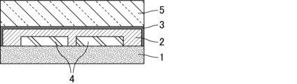
- FIG. 1 a schematic diagram showing an example of the laminate of the present invention is shown in FIG. 1.
- the laminate of the present invention has a structure in which an organic layer 2 and an inorganic layer 3 are laminated on a first element 1, and the organic layer 2 and the inorganic layer 3 act as an insulating layer when a plurality of laminates are laminated.
- Conventional laminates using organic compounds as insulating layers have a high effect of suppressing warping of elements due to heat treatment when a plurality of laminates are laminated to form a semiconductor device, but are prone to permeation of moisture in the atmosphere.
- the permeation of moisture can be suppressed by laminating a thin inorganic layer 3 containing Si 3 N 4 on the organic layer 2. Furthermore, in the laminate of the present invention, since the inorganic layer 3 has an internal stress in the compression direction, the difference in internal stress between the organic layer 2 and the inorganic layer 3 is small, and the occurrence of cracks in the inorganic layer can be suppressed. As a result, moisture is more difficult to permeate, and high connection reliability can be exhibited. In addition, since the thickness of the inorganic layer 3 in the laminate of the present invention is thin, the organic layer 2 does not hinder the elimination of the warping of the element. In addition, although the organic layer 2 and the inorganic layer 3 are each a single layer in FIG. 1, they may each be made up of a plurality of layers.
- the laminate of the present invention may be a laminate having multiple chips 4 on one surface (first surface) of a first element 1, and an organic layer 2 and an inorganic layer 3 laminated on the first surface of the first element.
- a support substrate 5 may be laminated on the inorganic layer 3.
- the method for producing the laminate of the present invention includes the steps of forming the organic layer by depositing a curable resin composition on a first element, and forming the inorganic layer having an internal stress in a compressive direction on the organic layer by chemical vapor deposition.
- the method for producing the laminate of the present invention also includes the steps of forming the inorganic layer having an internal stress in a compressive direction on the organic layer by chemical vapor deposition.
- the method for producing a laminate of the present invention first carries out a step of forming the organic layer by forming a film of a curable resin composition on a first element.
- Conventional laminates using inorganic materials for the insulating layer have been manufactured by time-consuming methods such as chemical vapor deposition (CVD) and sputtering. Since the main component of the insulating layer of the laminate of the present invention is an organic compound, it can be manufactured by applying and drying a solution, which not only improves connection reliability but also increases production efficiency.
- the first element and the curable resin composition are the same as the first element and the curable resin composition in the laminate of the present invention.
- the method for forming the film is not particularly limited, and a conventionally known method such as spin coating can be used.
- the solvent drying conditions are not particularly limited, but from the viewpoint of reducing the remaining solvent and improving the heat resistance of the organic layer, it is preferable to heat the organic layer at a temperature of preferably 70° C. or higher, more preferably 100° C. or higher, preferably 250° C. or lower, more preferably 200° C. or lower, for example, for 30 minutes, more preferably for about 1 hour.
- the curing conditions are not particularly limited, but from the viewpoint of sufficiently progressing the curing reaction and further improving the heat resistance, it is preferable to heat for, for example, about 1 hour or more, more preferably 2 hours or more at a temperature of preferably 200° C.
- the upper limit of the heating time is not particularly limited, but from the viewpoint of suppressing thermal decomposition of the organic layer, it is preferably 3 hours or less.
- the first element has a first surface and a second surface, the first surface has a plurality of chips, and in the step of forming the organic layer, the organic layer is formed on the first surface side.
- the method for producing a laminate of the present invention then includes the step of forming the inorganic layer having an internal stress in a compressive direction on the organic layer by chemical vapor deposition.
- An inorganic layer is formed on an organic layer by a chemical vapor deposition (CVD) method, and the conditions for the CVD method are adjusted to provide an inorganic layer having an internal stress in a compressive direction.
- the conditions for the inorganic layer and the CVD method are the same as those for the inorganic layer and the CVD method in the laminate of the present invention.
- the method for producing a laminate of the present invention preferably further comprises a step of laminating a support substrate onto the inorganic layer. By carrying out the step of bonding the supporting substrates, a laminate having the structure shown in FIG. 3 can be manufactured.
- the use of the laminate of the present invention is not particularly limited, but since the element is unlikely to warp or crack when laminated, has high moisture resistance, and can provide excellent connection reliability, it is suitable for imaging devices and semiconductor devices.
- Such an imaging device having the laminate of the present invention, a semiconductor device having the laminate of the present invention, and a method for manufacturing an imaging device having a step of manufacturing an imaging device using a laminate obtained by the method for manufacturing a laminate of the present invention are also one aspect of the present invention.
- the laminate of the present invention can also be used as a material for an element in which a plurality of laminates are stacked.
- the present invention also provides a method for manufacturing an element, the method including the steps of forming an organic layer by depositing a curable resin composition on a surface of a substrate having an electrode, the surface having the electrode, forming an inorganic layer having an internal stress in a compressive direction on the organic layer by chemical vapor deposition, forming through holes in the organic layer and the inorganic layer, filling the through holes with a conductive material, and polishing the surface of the substrate having an electrode on the side filled with the conductive material to form a bonding electrode.
- the method for manufacturing an element of the present invention first includes a step of forming an organic layer by depositing a curable resin composition on a surface of a substrate having an electrode, the surface having the electrode, and a step of forming an inorganic layer having an internal stress in a compressive direction on the organic layer by a chemical vapor deposition method.
- the step of forming the organic layer and the step of forming the inorganic layer are the same as those in the method for producing the laminate of the present invention.
- the substrate having the electrodes is not particularly limited, and a circuit substrate on which elements, wiring, and electrodes are formed can be used.
- a sensor circuit substrate on which a pixel section (pixel region) is provided, or a circuit substrate on which peripheral circuit sections such as logic circuits that perform various signal processing related to the operation of the solid-state imaging device are mounted can be used.
- the material of the electrodes of the substrate having the electrodes is not particularly limited, and conventionally known electrode materials such as gold, copper, and aluminum can be used.
- the method for producing an element of the present invention then carries out a step of forming through holes in the organic layer and the inorganic layer.
- the organic layer and inorganic layer on the electrode of the substrate are removed to provide a through hole, which is then filled with a conductive material to form a connection electrode for connecting to another substrate.
- the through hole may be patterned.
- the method for forming the through hole is not particularly limited, and the through hole may be formed by laser irradiation such as CO2 laser or etching.
- the through hole is formed so as to penetrate the other layers and expose the electrode surface of the element.
- the method for manufacturing an element of the present invention then includes the step of forming a barrier metal layer, if necessary.
- the barrier metal layer has a role of preventing the diffusion of the conductive material (e.g., Cu atoms in the case of a Cu electrode) filled in the through hole into the organic layer.
- the conductive material e.g., Cu atoms in the case of a Cu electrode
- the barrier metal layer can be formed by sputtering, vapor deposition, or the like.
- the barrier metal layer can be made of known materials such as tantalum, tantalum nitride, titanium nitride, silicon oxide, and silicon nitride.
- the thickness of the barrier metal layer is not particularly limited, but from the viewpoint of further improving the connection reliability of the laminate, it is preferably 1 nm or more, more preferably 10 nm or more, more preferably 100 nm or less, and even more preferably 50 nm or less.
- the method for manufacturing an element of the present invention then includes a step of filling each of the through holes with a conductive material, which can be performed by plating or the like.
- the conductive material may be the same as the material of the electrodes of the electrode-bearing substrate of the laminate of the present invention.
- the method for producing an element of the present invention then carries out a step of polishing the surface of the electrode-bearing substrate on the side filled with the conductive material to form a bonding electrode.
- the conductive material formed in the unnecessary portion is removed by grinding, thereby forming a bonding electrode to be connected to an electrode of another element.
- the polishing is preferably performed by planarizing and removing the layer formed of the conductive material until the inorganic layer is exposed.
- the polishing method is not particularly limited, and for example, a chemical mechanical polishing method can be used.
- the use of the element obtained by the element manufacturing method of the present invention is not particularly limited, but it is suitable for an imaging device having a semiconductor device in which elements are stacked.
- Such a method for manufacturing an imaging device which includes a step of manufacturing an imaging device using an element obtained by the element manufacturing method of the present invention, is also one aspect of the present invention.
- the element obtained by the element manufacturing method of the present invention is used for manufacturing a semiconductor device in which a plurality of elements are stacked with bonding electrodes.
- the present invention also includes a method for manufacturing a semiconductor device, which includes a step of bonding two elements obtained by the element manufacturing method of the present invention so that the connection electrodes are joined to each other.
- methods for connecting the connection electrodes include a method of melting and connecting the electrodes by heat treatment.
- the heat treatment is usually performed at 400°C for about 4 hours.
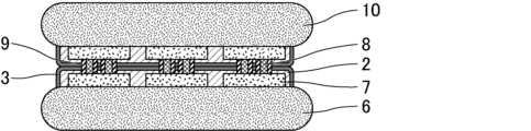
- FIG. 4 a schematic diagram showing an example of a semiconductor device obtained by the manufacturing method of a semiconductor device of the present invention is shown in FIG. 4.
- substrates 6 and 10 having electrodes 7 are bonded via an organic layer 2 and an inorganic layer 3, and the electrodes 7 on the substrates 6 and 10 having electrodes are electrically connected through a conductive material filled in a through hole 8 provided in the organic layer 2 and the inorganic layer 3.
- the semiconductor device may have a barrier metal layer 9 on the surface of the through hole 8. By forming the barrier metal layer 9 on the surface of the through hole 8, it becomes difficult for the conductive material filled in the through hole 8 to diffuse into the organic layer 2, so that short circuits and poor conduction can be further suppressed.
- the present invention provides a laminate that is resistant to warping or cracking of elements when stacked to form a semiconductor device, has high moisture resistance, and can provide excellent connection reliability, a method for manufacturing the laminate, a method for manufacturing elements using the laminate, an imaging device having the laminate, a method for manufacturing the imaging device, a semiconductor device having the laminate, and a method for manufacturing the semiconductor device.
- FIG. 1 is a schematic diagram showing an example of a laminate of the present invention.
- FIG. 1 is a schematic diagram showing an example of a laminate of the present invention.
- FIG. 1 is a schematic diagram showing an example of a laminate of the present invention.
- 1 is a schematic diagram showing an example of a semiconductor device obtained by a method for producing a semiconductor device according to the present invention;
- Example 1 (1) Production of Organosilicon Compound A 65.4 g of phenyltrimethoxysilane (manufactured by Tokyo Chemical Industry Co., Ltd., molecular weight 198.29), 8.8 g of sodium hydroxide, 6.6 g of water, and 263 mL of 2-propanol were added to a reaction vessel equipped with a reflux condenser, a thermometer, and a dropping funnel. Heating was started with stirring under a nitrogen stream. Stirring was continued for 6 hours from the start of reflux, and then the mixture was allowed to stand overnight at room temperature. The reaction mixture was then transferred to a filter, pressurized with nitrogen gas, and filtered. The obtained solid was washed once with 2-propyl alcohol, filtered, and then dried under reduced pressure at 80°C to obtain 33.0 g of a colorless solid (DD-ONa).
- a colorless solid DD-ONa
- the reaction mixture thus obtained was separated, and the organic layer was washed once with 1N hydrochloric acid, once with a saturated aqueous solution of sodium bicarbonate, and then washed three times with ion-exchanged water.
- the washed organic layer was dried over anhydrous magnesium sulfate and concentrated under reduced pressure using a rotary evaporator to obtain 7.1 g of a white powdery solid (DD(Me)-OH).
- a 100 mL flask was fitted with a cooling tube, mechanical stirrer, Dean-Stark tube, oil bath and thermometer protection tube, and the inside of the flask was replaced with nitrogen.
- 5.0 g of DD(Me)-OH, 11.6 g of octamethylcyclotetrasiloxane (D4), 3.9 g of sulfuric acid, 52 g of toluene and 13 g of 4-methyltetrahydropyran were placed in the flask. After stirring at 100°C for 5 hours, water was poured into the reaction mixture and the aqueous layer was extracted with toluene.
- organosilicon compound A (weight average molecular weight: 36,000) having the structure of the following formula (8), m being 27 and n being an average of 4.
- a curable resin composition was obtained by adding and mixing 100 parts by weight of the obtained organosilicon compound, 0.2 parts by weight of a catalyst (ZC-162, an acetylacetonate complex having a zirconium central metal, manufactured by Matsumoto Fine Chemical Co., Ltd.), 3.2 parts by weight of a crosslinking agent (methyl silicate 51, manufactured by Colcoat Co., Ltd.) and 1 part by weight of additive A with a solvent (cyclopentanone, manufactured by Tokyo Chemical Industry Co., Ltd.) so that the content was 65% by weight.
- a catalyst ZC-162
- an acetylacetonate complex having a zirconium central metal manufactured by Matsumoto Fine Chemical Co., Ltd.
- a crosslinking agent methyl silicate 51, manufactured by Colcoat Co., Ltd.
- additive A cyclopentanone, manufactured by Tokyo Chemical Industry Co., Ltd.
- inorganic film formation was performed by CVD for a predetermined time under the conditions shown in Table 3 using PE-CVD (part number MPX-CVD, manufactured by Sumitomo Precision Products Co., Ltd.), and a SiN layer (inorganic layer) having a thickness of 400 nm was formed on the organic layer to obtain a laminate.
- PE-CVD part number MPX-CVD, manufactured by Sumitomo Precision Products Co., Ltd.
- the radius of curvature R at this time was designated as R2 .
- the inorganic film stress S (Pa) was calculated from the Stoney formula represented by the following formula (A). The results are shown in Table 1.
- the numerical value of the film stress is a negative value, it indicates that there is an internal stress in the compressive direction, and when it is a positive value, it indicates that there is an internal stress in the tensile direction.
- E/(1-v) Biaxial elastic modulus (Pa) of the silicon wafer, which was set to 1.805 ⁇ 10 11 Pa.
- h thickness (m) of the silicon wafer, which was set to 725 ⁇ m.
- t thickness of the inorganic film (m), which was set to 100 nm.
- R the radius of curvature of the substrate, which is obtained from the following formula (B).
- Examples 2 to 19, Comparative Examples 1 to 6 A laminate was obtained under the same conditions as in Example 1, except that the configurations of the organic layer and the inorganic layer and the film-forming conditions were as shown in Tables 1 to 3, and the 1% thermal weight loss temperature, internal stress, P2180/P775, and P1200/P775 were measured.
- Comparative Example 6 dibutyltin dilaurate (manufactured by Tokyo Chemical Industry Co., Ltd.) was used as the catalyst.
- ethyl silicate 48 manufactured by Colcoat Co., Ltd.
- resin B and additives B to D were resins, additives, or commercially available products obtained by the following methods.
- film-forming conditions 10 to 12 a PD-220NL (manufactured by Samco Co., Ltd.) was used as the film-forming device.
- the combined organic layer was washed with water, an aqueous sodium bicarbonate solution, and saturated saline, and then dried over anhydrous sodium sulfate.
- the mixture was refluxed in an oil bath at 170°C for 2 hours, and the resulting synthetic liquid was cooled to room temperature, and then filtered using a membrane filter (product number: ADVANTEC T080A075C, manufactured by Toyo Roshi Co., Ltd.) to obtain an additive B having the structure of the following formula (10) as a precipitate.
- a membrane filter product number: ADVANTEC T080A075C, manufactured by Toyo Roshi Co., Ltd.
- additives C and D The following additives were used as additives C and D, respectively.
- Additive C TC-401 (manufactured by Matsumoto Fine Chemical Co., Ltd.)
- Additive D BYK-320 (manufactured by BYK Corporation)
- the laminate was heat-treated in a nitrogen atmosphere at 400° C. for 3 hours in a vacuum process high speed heating furnace (VPO-650, manufactured by Unitemp Co., Ltd.)
- VPO-650 vacuum process high speed heating furnace
- the laminate after heat treatment was evaluated for film cracking in the thick film according to the following criteria. ⁇ : No cracks were found after heat treatment. ⁇ : Cracks of about 2 mm were found at the ends after heat treatment. ⁇ : Cracks were found after heat treatment.
- the laminate was left to stand for 500 hours in an environment of a temperature of 85° C. and a humidity of 85%. Thereafter, the laminate was visually observed, and the moisture resistance was evaluated according to the following criteria. ⁇ : No trace of water intrusion from the edge was observed. ⁇ : Trace of water intrusion from the edge was less than 2 mm. ⁇ : Trace of water intrusion from the edge was 2 mm or more but less than 4 mm. ⁇ : Trace of water intrusion from the edge was 4 mm or more.
- the present invention provides a laminate that is resistant to warping or cracking of elements when stacked to form a semiconductor device, has high moisture resistance, and can provide excellent connection reliability, a method for manufacturing the laminate, a method for manufacturing elements using the laminate, an imaging device having the laminate, a method for manufacturing the imaging device, a semiconductor device having the laminate, and a method for manufacturing the semiconductor device.
Landscapes
- Chemical & Material Sciences (AREA)
- Chemical Kinetics & Catalysis (AREA)
- Organic Chemistry (AREA)
- Engineering & Computer Science (AREA)
- Medicinal Chemistry (AREA)
- Polymers & Plastics (AREA)
- Health & Medical Sciences (AREA)
- Life Sciences & Earth Sciences (AREA)
- Materials Engineering (AREA)
- Wood Science & Technology (AREA)
- Solid State Image Pick-Up Elements (AREA)
- Laminated Bodies (AREA)
- Manufacturing & Machinery (AREA)
- Physics & Mathematics (AREA)
- Geometry (AREA)
Priority Applications (4)
| Application Number | Priority Date | Filing Date | Title |
|---|---|---|---|
| EP24747242.6A EP4656377A1 (en) | 2023-01-23 | 2024-01-22 | Laminated body, method for manufacturing laminated body, method for manufacturing element, imaging device, method for manufacturing imaging device, semiconductor device, and method for manufacturing semiconductor device |
| CN202480005219.2A CN120225353A (zh) | 2023-01-23 | 2024-01-22 | 层叠体、层叠体的制造方法、元件的制造方法、拍摄装置、拍摄装置的制造方法、半导体装置和半导体装置的制造方法 |
| JP2024506204A JPWO2024157914A1 (https=) | 2023-01-23 | 2024-01-22 | |
| KR1020257019165A KR20250141127A (ko) | 2023-01-23 | 2024-01-22 | 적층체, 적층체의 제조 방법, 소자의 제조 방법, 촬상 장치, 촬상 장치의 제조 방법, 반도체 장치 및 반도체 장치의 제조 방법 |
Applications Claiming Priority (2)
| Application Number | Priority Date | Filing Date | Title |
|---|---|---|---|
| JP2023-008163 | 2023-01-23 | ||
| JP2023008163 | 2023-01-23 |
Publications (1)
| Publication Number | Publication Date |
|---|---|
| WO2024157914A1 true WO2024157914A1 (ja) | 2024-08-02 |
Family
ID=91970667
Family Applications (1)
| Application Number | Title | Priority Date | Filing Date |
|---|---|---|---|
| PCT/JP2024/001591 Ceased WO2024157914A1 (ja) | 2023-01-23 | 2024-01-22 | 積層体、積層体の製造方法、素子の製造方法、撮像装置、撮像装置の製造方法、半導体装置及び半導体装置の製造方法 |
Country Status (6)
| Country | Link |
|---|---|
| EP (1) | EP4656377A1 (https=) |
| JP (1) | JPWO2024157914A1 (https=) |
| KR (1) | KR20250141127A (https=) |
| CN (1) | CN120225353A (https=) |
| TW (1) | TW202440795A (https=) |
| WO (1) | WO2024157914A1 (https=) |
Citations (10)
| Publication number | Priority date | Publication date | Assignee | Title |
|---|---|---|---|---|
| JPH06260397A (ja) * | 1993-03-08 | 1994-09-16 | Toppan Printing Co Ltd | X線露光用マスクとその製造方法 |
| JPH11271123A (ja) * | 1998-03-20 | 1999-10-05 | Denso Corp | マイクロヒータおよびその製造方法ならびにエアフローセンサ |
| JP2005149751A (ja) * | 2003-11-11 | 2005-06-09 | Olympus Corp | 発熱素子 |
| JP2006191081A (ja) | 2004-12-30 | 2006-07-20 | Magnachip Semiconductor Ltd | 受光領域が拡張されたイメージセンサ及びその製造方法 |
| JP2007125626A (ja) * | 2005-11-01 | 2007-05-24 | Toshiba Corp | Mems素子 |
| WO2009041528A1 (ja) * | 2007-09-26 | 2009-04-02 | Citizen Holdings Co., Ltd. | 時計用カバーガラス |
| JP2009152485A (ja) * | 2007-12-21 | 2009-07-09 | Seiko Epson Corp | 半導体装置の製造方法及び半導体装置 |
| JP2019196936A (ja) * | 2018-05-08 | 2019-11-14 | 日立オートモティブシステムズ株式会社 | 熱式センサ装置 |
| JP2022504537A (ja) * | 2018-10-09 | 2022-01-13 | フラウンホーファー-ゲゼルシャフト・ツール・フェルデルング・デル・アンゲヴァンテン・フォルシュング・アインゲトラーゲネル・フェライン | 集積キャパシタおよび集積キャパシタの製造方法 |
| JP7144624B2 (ja) * | 2020-06-22 | 2022-09-29 | 積水化学工業株式会社 | 積層体、硬化性樹脂組成物、積層体の製造方法、接合電極を有する基板の製造方法、半導体装置及び撮像装置 |
-
2024
- 2024-01-22 JP JP2024506204A patent/JPWO2024157914A1/ja active Pending
- 2024-01-22 WO PCT/JP2024/001591 patent/WO2024157914A1/ja not_active Ceased
- 2024-01-22 KR KR1020257019165A patent/KR20250141127A/ko active Pending
- 2024-01-22 CN CN202480005219.2A patent/CN120225353A/zh active Pending
- 2024-01-22 EP EP24747242.6A patent/EP4656377A1/en active Pending
- 2024-01-23 TW TW113102545A patent/TW202440795A/zh unknown
Patent Citations (10)
| Publication number | Priority date | Publication date | Assignee | Title |
|---|---|---|---|---|
| JPH06260397A (ja) * | 1993-03-08 | 1994-09-16 | Toppan Printing Co Ltd | X線露光用マスクとその製造方法 |
| JPH11271123A (ja) * | 1998-03-20 | 1999-10-05 | Denso Corp | マイクロヒータおよびその製造方法ならびにエアフローセンサ |
| JP2005149751A (ja) * | 2003-11-11 | 2005-06-09 | Olympus Corp | 発熱素子 |
| JP2006191081A (ja) | 2004-12-30 | 2006-07-20 | Magnachip Semiconductor Ltd | 受光領域が拡張されたイメージセンサ及びその製造方法 |
| JP2007125626A (ja) * | 2005-11-01 | 2007-05-24 | Toshiba Corp | Mems素子 |
| WO2009041528A1 (ja) * | 2007-09-26 | 2009-04-02 | Citizen Holdings Co., Ltd. | 時計用カバーガラス |
| JP2009152485A (ja) * | 2007-12-21 | 2009-07-09 | Seiko Epson Corp | 半導体装置の製造方法及び半導体装置 |
| JP2019196936A (ja) * | 2018-05-08 | 2019-11-14 | 日立オートモティブシステムズ株式会社 | 熱式センサ装置 |
| JP2022504537A (ja) * | 2018-10-09 | 2022-01-13 | フラウンホーファー-ゲゼルシャフト・ツール・フェルデルング・デル・アンゲヴァンテン・フォルシュング・アインゲトラーゲネル・フェライン | 集積キャパシタおよび集積キャパシタの製造方法 |
| JP7144624B2 (ja) * | 2020-06-22 | 2022-09-29 | 積水化学工業株式会社 | 積層体、硬化性樹脂組成物、積層体の製造方法、接合電極を有する基板の製造方法、半導体装置及び撮像装置 |
Non-Patent Citations (1)
| Title |
|---|
| See also references of EP4656377A1 |
Also Published As
| Publication number | Publication date |
|---|---|
| CN120225353A (zh) | 2025-06-27 |
| JPWO2024157914A1 (https=) | 2024-08-02 |
| KR20250141127A (ko) | 2025-09-26 |
| EP4656377A1 (en) | 2025-12-03 |
| TW202440795A (zh) | 2024-10-16 |
Similar Documents
| Publication | Publication Date | Title |
|---|---|---|
| CN1125138C (zh) | 用于制造绝缘薄膜的烷氧基硅烷/有机聚合物组合物及其用途 | |
| US6225238B1 (en) | Low dielectric constant polyorganosilicon coatings generated from polycarbosilanes | |
| JP7522910B2 (ja) | 硬化性樹脂組成物、硬化膜、積層体、撮像装置、半導体装置、積層体の製造方法及び接合電極を有する素子の製造方法 | |
| TWI891818B (zh) | 積層體、硬化性樹脂組成物、積層體之製造方法、具有接合電極之基板的製造方法、半導體裝置及攝影裝置 | |
| KR20080026136A (ko) | 탄화수소 기를 브릿징으로 작용기화된 실란 모노머를중합하는 것을 포함하는 반도체 광학장치를 위한 폴리머를제조하는 방법 | |
| WO2025063069A1 (ja) | 硬化性樹脂組成物、硬化膜、積層体及び半導体装置 | |
| JP2001287910A (ja) | 多孔質ケイ素酸化物塗膜の製造方法 | |
| WO2024157914A1 (ja) | 積層体、積層体の製造方法、素子の製造方法、撮像装置、撮像装置の製造方法、半導体装置及び半導体装置の製造方法 | |
| JP2025007848A (ja) | 硬化性フィルムの製造方法、硬化性フィルム、積層体、撮像装置、半導体装置及び積層体の製造方法 | |
| JP2023094125A (ja) | 樹脂硬化物、硬化性樹脂組成物、積層体、撮像装置、半導体装置、積層体の製造方法及び接合電極を有する素子の製造方法 | |
| JP2002201415A (ja) | シリカ系被膜形成用塗布液、シリカ系被膜の製造方法及び半導体装置 | |
| CN118055981A (zh) | 固化性树脂组合物、固化膜、层叠体、拍摄装置、半导体装置、层叠体的制造方法和具有接合电极的元件的制造方法 | |
| WO2025009514A1 (ja) | 硬化性樹脂組成物、硬化膜、積層体、撮像装置、半導体装置及び積層体の製造方法 | |
| JPH11217440A (ja) | フルオロアルキル基含有ポリシロキサン、低誘電率樹脂組成物及び物品 | |
| WO2024157936A1 (ja) | 樹脂組成物、硬化膜、積層体、撮像装置、半導体装置、積層体の製造方法及び接合電極を有する素子の製造方法 | |
| JP2024013537A (ja) | 硬化性樹脂組成物、硬化膜、積層体、撮像装置及び半導体装置の製造方法 |
Legal Events
| Date | Code | Title | Description |
|---|---|---|---|
| WWE | Wipo information: entry into national phase |
Ref document number: 2024506204 Country of ref document: JP |
|
| 121 | Ep: the epo has been informed by wipo that ep was designated in this application |
Ref document number: 24747242 Country of ref document: EP Kind code of ref document: A1 |
|
| WWE | Wipo information: entry into national phase |
Ref document number: 202480005219.2 Country of ref document: CN |
|
| WWP | Wipo information: published in national office |
Ref document number: 202480005219.2 Country of ref document: CN |
|
| NENP | Non-entry into the national phase |
Ref country code: DE |
|
| WWP | Wipo information: published in national office |
Ref document number: 2024747242 Country of ref document: EP |