WO2024127535A1 - プラズマ処理方法 - Google Patents
プラズマ処理方法 Download PDFInfo
- Publication number
- WO2024127535A1 WO2024127535A1 PCT/JP2022/045949 JP2022045949W WO2024127535A1 WO 2024127535 A1 WO2024127535 A1 WO 2024127535A1 JP 2022045949 W JP2022045949 W JP 2022045949W WO 2024127535 A1 WO2024127535 A1 WO 2024127535A1
- Authority
- WO
- WIPO (PCT)
- Prior art keywords
- region
- etching
- plasma
- plasma processing
- magnetic field
- Prior art date
- Legal status (The legal status is an assumption and is not a legal conclusion. Google has not performed a legal analysis and makes no representation as to the accuracy of the status listed.)
- Ceased
Links
Images






Classifications
-
- H—ELECTRICITY
- H01—ELECTRIC ELEMENTS
- H01J—ELECTRIC DISCHARGE TUBES OR DISCHARGE LAMPS
- H01J37/00—Discharge tubes with provision for introducing objects or material to be exposed to the discharge, e.g. for the purpose of examination or processing thereof
- H01J37/32—Gas-filled discharge tubes
- H01J37/32431—Constructional details of the reactor
- H01J37/3266—Magnetic control means
- H01J37/32678—Electron cyclotron resonance
-
- H—ELECTRICITY
- H01—ELECTRIC ELEMENTS
- H01J—ELECTRIC DISCHARGE TUBES OR DISCHARGE LAMPS
- H01J37/00—Discharge tubes with provision for introducing objects or material to be exposed to the discharge, e.g. for the purpose of examination or processing thereof
- H01J37/32—Gas-filled discharge tubes
-
- H—ELECTRICITY
- H01—ELECTRIC ELEMENTS
- H01J—ELECTRIC DISCHARGE TUBES OR DISCHARGE LAMPS
- H01J37/00—Discharge tubes with provision for introducing objects or material to be exposed to the discharge, e.g. for the purpose of examination or processing thereof
- H01J37/32—Gas-filled discharge tubes
- H01J37/32431—Constructional details of the reactor
- H01J37/3244—Gas supply means
-
- H—ELECTRICITY
- H01—ELECTRIC ELEMENTS
- H01J—ELECTRIC DISCHARGE TUBES OR DISCHARGE LAMPS
- H01J37/00—Discharge tubes with provision for introducing objects or material to be exposed to the discharge, e.g. for the purpose of examination or processing thereof
- H01J37/32—Gas-filled discharge tubes
- H01J37/32431—Constructional details of the reactor
- H01J37/3244—Gas supply means
- H01J37/32449—Gas control, e.g. control of the gas flow
-
- H—ELECTRICITY
- H10—SEMICONDUCTOR DEVICES; ELECTRIC SOLID-STATE DEVICES NOT OTHERWISE PROVIDED FOR
- H10P—GENERIC PROCESSES OR APPARATUS FOR THE MANUFACTURE OR TREATMENT OF DEVICES COVERED BY CLASS H10
- H10P50/00—Etching of wafers, substrates or parts of devices
- H10P50/20—Dry etching; Plasma etching; Reactive-ion etching
- H10P50/28—Dry etching; Plasma etching; Reactive-ion etching of insulating materials
-
- H—ELECTRICITY
- H10—SEMICONDUCTOR DEVICES; ELECTRIC SOLID-STATE DEVICES NOT OTHERWISE PROVIDED FOR
- H10P—GENERIC PROCESSES OR APPARATUS FOR THE MANUFACTURE OR TREATMENT OF DEVICES COVERED BY CLASS H10
- H10P50/00—Etching of wafers, substrates or parts of devices
- H10P50/20—Dry etching; Plasma etching; Reactive-ion etching
- H10P50/28—Dry etching; Plasma etching; Reactive-ion etching of insulating materials
- H10P50/282—Dry etching; Plasma etching; Reactive-ion etching of insulating materials of inorganic materials
- H10P50/283—Dry etching; Plasma etching; Reactive-ion etching of insulating materials of inorganic materials by chemical means
-
- H—ELECTRICITY
- H10—SEMICONDUCTOR DEVICES; ELECTRIC SOLID-STATE DEVICES NOT OTHERWISE PROVIDED FOR
- H10P—GENERIC PROCESSES OR APPARATUS FOR THE MANUFACTURE OR TREATMENT OF DEVICES COVERED BY CLASS H10
- H10P72/00—Handling or holding of wafers, substrates or devices during manufacture or treatment thereof
-
- H—ELECTRICITY
- H10—SEMICONDUCTOR DEVICES; ELECTRIC SOLID-STATE DEVICES NOT OTHERWISE PROVIDED FOR
- H10P—GENERIC PROCESSES OR APPARATUS FOR THE MANUFACTURE OR TREATMENT OF DEVICES COVERED BY CLASS H10
- H10P72/00—Handling or holding of wafers, substrates or devices during manufacture or treatment thereof
- H10P72/04—Apparatus for manufacture or treatment
- H10P72/0402—Apparatus for fluid treatment
- H10P72/0418—Apparatus for fluid treatment for etching
- H10P72/0421—Apparatus for fluid treatment for etching for drying etching
-
- H—ELECTRICITY
- H01—ELECTRIC ELEMENTS
- H01J—ELECTRIC DISCHARGE TUBES OR DISCHARGE LAMPS
- H01J2237/00—Discharge tubes exposing object to beam, e.g. for analysis treatment, etching, imaging
- H01J2237/32—Processing objects by plasma generation
- H01J2237/33—Processing objects by plasma generation characterised by the type of processing
- H01J2237/334—Etching
- H01J2237/3341—Reactive etching
-
- H—ELECTRICITY
- H10—SEMICONDUCTOR DEVICES; ELECTRIC SOLID-STATE DEVICES NOT OTHERWISE PROVIDED FOR
- H10P—GENERIC PROCESSES OR APPARATUS FOR THE MANUFACTURE OR TREATMENT OF DEVICES COVERED BY CLASS H10
- H10P50/00—Etching of wafers, substrates or parts of devices
- H10P50/20—Dry etching; Plasma etching; Reactive-ion etching
- H10P50/24—Dry etching; Plasma etching; Reactive-ion etching of semiconductor materials
- H10P50/242—Dry etching; Plasma etching; Reactive-ion etching of semiconductor materials of Group IV materials
Definitions
- the present invention relates to a plasma processing method.
- Patent Document 1 proposes a technology for an etching process for forming grooves in a semiconductor substrate, in which a first process is performed under conditions with a high etching rate immediately after etching starts, and then a second process is performed under conditions with a low etching rate.
- Patent Document 2 also proposes a technique that involves repeatedly performing an etching process in which roughness is formed on the etched surface of a substrate by anisotropic etching mainly using ions, followed by a process of removing the roughness formed by the above process by isotropic etching mainly using radicals from a gas that is non-depositive on the substrate.
- JP 2015-153804 A Japanese Patent Application Laid-Open No. 3-93224
- Patent Document 1 has the same problem of suppressing variation in the amount of etching in sparse and dense patterns, the means of solving the problem differs from that of the present invention.
- Patent Document 2 involves repeating ionic etching and radical etching in order to achieve both verticality and smoothness of the pattern after etching, and does not attempt to independently control the etching shape of the sparse and dense parts of the pattern.
- the present invention provides a plasma processing method that solves the problems of the conventional technology described above and enables uniform etching of sparse and dense portions of a pattern on the same wafer.
- the present invention provides a plasma processing method that includes a first step of performing reactive ion etching using a gas that forms a tapered shape, and a second step of performing radical etching, in which the first step and the second step are alternately repeated a predetermined number of times, and the time for the first step is shorter than the time for the second step.
- the present invention it is possible to independently control the etching shapes of sparse and dense portions of a pattern on the same wafer, making it possible to etch the sparse and dense portions uniformly.
- FIG. 1 is a vertical cross-sectional view showing an outline of a plasma etching apparatus according to a first embodiment of the present invention
- FIG. 2 is a plan view showing a shielding plate of the plasma etching apparatus according to the first embodiment of the present invention.
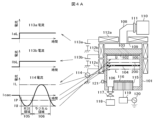
- FIG. 4 is a diagram showing a current for setting a central ECR region by a DC coil current power supply according to the first embodiment of the present invention.
- FIG. 4 is a diagram showing a current for setting a central ECR region by a DC coil current power supply according to the first embodiment of the present invention.
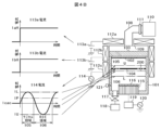
- 3B is a diagram showing the current of an AC coil current power supply that moves the ECR region up and down relative to the ion shielding plate, with the ECR region in FIG. 3A being set as an initial setting position.
- 3C is a diagram showing the current of an AC coil current power supply that moves the ECR region up and down relative to the ion shielding plate, with the ECR region in FIG. 3B being the initial setting position.
- 5A to 5C are schematic diagrams showing an etching shape that indicates that the etching shapes of the sparsely and densely etched portions can be independently controlled by controlling the RIE time ratio according to the first embodiment of the present invention.
- 1 is a graph showing that taper angles of sparse and dense portions can be made uniform by controlling the RIE time ratio according to the first embodiment of the present invention.
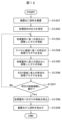
- FIG. 2 is a flow chart showing a process flow of the plasma etching method according to the first embodiment of the present invention.
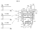
- FIG. 11 is a vertical cross-sectional view showing an outline of a plasma etching apparatus according to a modified example of the first embodiment of the FIG. 11 is a diagram showing a current for setting an ECR region corresponding to the center frequency of a power supply for generating variable frequency electromagnetic waves by a DC coil current power supply according to a modified example of the first embodiment of the present invention.
- FIG. 11 is a diagram showing a current for setting an ECR region corresponding to the center frequency of a power supply for generating variable frequency electromagnetic waves by a DC coil current power supply according to a modified example of the first embodiment of the present invention.
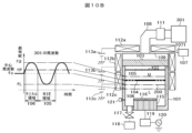
- FIG. 9B is a diagram showing the current of an AC coil current power supply that raises and lowers the ECR region relative to the ion shielding plate by changing the frequency of a variable frequency electromagnetic wave generating power supply centered on the ECR region of the center frequency set in FIG. 9A.
- FIG. 9C is a diagram showing the current of an AC coil current power supply that raises and lowers the ECR region relative to the ion shielding plate by changing the frequency of a variable frequency electromagnetic wave generating power supply centered on the ECR region of the center frequency set in FIG. 9B.
- FIG. 11 is a vertical cross-sectional view showing an outline of a plasma etching apparatus according to a second embodiment of the present invention.
- FIG. 11 is a flowchart showing a process flow of a plasma etching method according to a second embodiment of the present invention.
- the present invention uses a plasma processing apparatus equipped with a gas system that etches a tapered shape in RIE and also allows etching to proceed in radical etching, where the same gas system is used to shield ions, and by repeatedly performing RIE processing and radical etching processing while controlling it, it is possible to uniformly etch sparse and dense portions of a pattern on the same wafer.
- the present invention also uses a plasma processing apparatus equipped with a gas system that etches a tapered shape in RIE and also allows etching to proceed in radical etching in which ions are shielded using the same gas system.
- RIE time ratio the ratio of the RIE processing time to the total processing time of RIE and radical etching
- FIG. 1 is a vertical cross-sectional view showing an outline of the overall configuration of a plasma processing apparatus according to this embodiment.
- the plasma processing apparatus 10 shown in FIG. 1 has a processing chamber 100 formed inside a vacuum vessel 101.
- a shower plate 102 for introducing an etching gas into the processing chamber 100 inside the vacuum vessel 101, a dielectric window 103 for airtightly sealing the top of the processing chamber 100, and an ion shielding plate 104 are installed at the top of the vacuum vessel 101 to form the processing chamber 100.
- a gas supply device 107 is connected to the region 1020 between the shower plate 102 and the dielectric window 103 via a gas supply pipe 1071, and gas for performing plasma etching processing is supplied.
- the shower plate 102 has a plurality of small holes 1021 formed therein for passing the gas supplied to the region 1020 to the processing chamber 100 side.
- a vacuum exhaust device 118 is connected to the vacuum vessel 101 via a pressure adjustment valve 117, and controls the pressure of the processing chamber 100. The pressure of the processing chamber 100 is measured by a pressure gauge 121.
- a waveguide 108 that radiates electromagnetic waves is provided above the dielectric window 103.
- Electromagnetic waves oscillated from an electromagnetic wave generating power source (also called a high frequency power source) 110 are transmitted to the waveguide 108 (or antenna) through an electromagnetic wave matching device 111.
- the frequency of the high frequency current output from the electromagnetic wave generating power source 110 is set to a constant frequency.
- a cavity resonator 109 is arranged to form a standing wave of a specific mode in the processing chamber 100 by the electromagnetic waves propagating from the waveguide 108.
- the frequency of the electromagnetic waves is not particularly limited, but in this embodiment, it is a microwave of 2.45 GHz.
- magnetic field generating coils 112a, 112b, and 112c are provided, and in order to control the current, DC coil current power supplies 113a and 113b are connected to the magnetic field generating coils 112a and 112b, and an AC coil current power supply 114 is connected to the magnetic field generating coil 112c.
- the magnetic field generating coils 112a and 112b are driven by the DC current output from the DC coil current power supplies 113a and 113b, and the magnetic field generating coil 112c is driven by the AC current output from the AC coil current power supply 114.
- the magnetic field generating coil 112, the DC coil current power supplies 113a and 113b, and the AC coil current power supply 114 can be referred to as a magnetic field forming mechanism.
- the magnetic field generating coils 112a and 112b can be referred to as the first coil, and the magnetic field generating coil 112c can be referred to as the second coil.
- the power generated by the electromagnetic wave generating power supply 110 generates plasma in the processing chamber 100 through electron cyclotron resonance (ECR) with the magnetic field formed by the magnetic field generating coil 112.
- ECR electron cyclotron resonance
- a substrate electrode 115 which also serves as a stage (also called a sample stage) for placing a sample (semiconductor substrate) 116, is installed at the bottom of the processing chamber 100 facing the ion shielding plate 104.
- a high-frequency power supply 120 is connected to the substrate electrode 115 via a high-frequency matching box 119.
- a negative voltage generally called a self-bias is generated on the substrate electrode 115, and the ions in the plasma are accelerated by the self-bias and are perpendicularly incident on the sample 116 placed on the substrate electrode 115, thereby etching the sample 116.
- the ion shielding plate 104 divides the internal space of the processing chamber 100 into upper and lower regions.
- the region between the ion shielding plate 104 and the shower plate 102 above in the internal space of the processing chamber 100 is referred to as the first region or radical region 105
- the region below the ion shielding plate 104 on the side where the substrate electrode 115 is installed is referred to as the second region or RIE (Reactive Ion Etching) region 106.
- the magnetic field generating coils 112a and 112b are disposed above the ion shielding plate 104.
- the magnetic field generating coil 112c is disposed below the magnetic field generating coils 112a and 112b, and is disposed near the ion shielding plate 104.
- the ion shielding plate 104 has through holes 1041 of the same diameter uniformly arranged around the periphery.
- "uniformly" means that when multiple concentric circles (including the case where the radius is zero) with the same difference in diameter are drawn, the through holes 1041 having their center points on the circumference of each concentric circle are arranged at equal pitch in the circumferential direction.
- radical region 105 When plasma is generated in the radical region 105, ions generated in the plasma are confined in the radical region 105 by the ion shielding plate 104. Meanwhile, radicals generated in the plasma diffuse inside the radical region 105, and some of them reach the RIE region 106 through the through-holes 1041 in the ion shielding plate 104.
- the magnetic field generating coil 112 has a self-inductance of 100 to 1000 mH, and the DC coil current power supplies 113a and 113b and the AC coil current power supply 114 are capable of supplying currents of approximately 10 to 60 A.
- the position of the ECR area in the processing chamber 100 can be precisely controlled, and the plasma generation position relative to the sample 116 can be moved.
- the magnetic field generating coils 112a and 112b are positioned above the ion shielding plate 104, the magnetic field strength created by these magnetic field generating coils 112a and 112b is stronger in the radical region 105, which is closer to the magnetic field generating coils 112a and 112b, than in the RIE region 106.
- the processing chamber 100 is equipped with an ion shielding plate 104 between the shower plate 102 and the substrate electrode 115, which is a support for the sample 116, and is divided into two regions: a radical region 105 above the ion shielding plate 104 and an RIE region 106 below the ion shielding plate 104.
- the ion shielding plate 104 When the ECR region is positioned within the radical region 105 and plasma is generated, the ion shielding plate 104 is between the sample 116 and the plasma, so the ions in the plasma generated in the approximate center of the radical region 105 are constrained by the magnetic field of the ECR region and do not diffuse, but are blocked near the center of the ion shielding plate 104 and are confined within the radical region 105. As a result, ions from the plasma do not reach the sample 116 on the side of the RIE region 106.
- the radicals generated within the radical region 105 diffuse within the radical region 105 without being constrained by the magnetic field of the ECR region, and some of them pass through the numerous through holes 1041 formed around the periphery of the ion shielding plate 104, so that the radicals are supplied to the side of the RIE region 106, and the sample 116 is plasma-processed by radical etching (isotropic etching).
- the control unit 130 is connected to the gas supply unit 107, pressure adjustment valve 117, electromagnetic wave generating power supply 110, DC coil current power supplies 113a and 113b, AC coil current power supply 114, and high frequency power supply 120, and controls the plasma processing apparatus 10 according to the process conditions. In the case of process conditions consisting of multiple plasma processing steps, the control unit 130 controls each device parameter in sequence according to each processing step, thereby etching the sample 116. In addition, information regarding the pressure inside the processing chamber 100 measured by the pressure gauge 121 is sent to the control unit 130, and is used to control the process conditions consisting of multiple plasma processing steps.
- the amount of ions supplied to the sample 116 is proportional to the ratio of the time set in the RIE region 106 to the time of one period during which the position of the ECR region is periodically switched between the radical region 105 and the RIE region 106 across the ion shielding plate 104.
- the center position of the ECR region is set by a DC current output from DC coil current power supplies (also called DC power supplies) 113a, 113b and applied to magnetic field generating coils 112a and 112b, and the position of the ECR region is raised or lowered by an AC current output from AC coil current power supply (also called AC power supply) 114 and applied to magnetic field generating coil 112c.
- DC coil current power supplies also called DC power supplies
- AC power supply also called AC power supply
- DC coil current power supplies 113a and 113b and AC coil current power supply 114 only the magnetic field generating coil 112c, which is closest to the ion shielding plate 104, is connected to the AC coil current power supply 114, and the magnetic field generating coils 112a and 112b, which are farther from the ion shielding plate 104 than the magnetic field generating coil 112c, are connected to the DC coil current power supplies 113a and 113b.
- FIGS 3A and 3B show an example in which the position of the ECR region is set by DC coil current power supplies 113a and 113b when the output from AC coil current power supply 114 is zero. Note that the position of the ECR region can also be considered as the center position of the ECR region.
- the magnetic field generated by the magnetic field generating coils 112a and 112b becomes weaker from the radical region 105 toward the RIE region 106, and a magnetic field stronger than the magnetic field strength of the ECR region is generated at the top of the vacuum vessel 101 (or processing chamber 100), so the greater the current, the further the ECR region moves downward in the vacuum vessel 101 (or processing chamber 100).
- Figures 4A and 4B show an example of raising and lowering the ECR region by passing an alternating current Icac through magnetic field generating coil 112c relative to the position 200 of the ECR region that is initially set by passing a current IaL through magnetic field generating coil 112a and a current IbL through magnetic field generating coil 112b.
- the position of the ECR region can be moved below the ion shielding plate 104 inside the vacuum vessel 101 (or processing chamber 100) when the AC current Icac flowing through the magnetic field generating coil 112c is positive, and moved above the ion shielding plate 104 when it is negative.
- the position 200 of the ECR region can be moved periodically between the radical region 105 and the RIE region 106 more efficiently (in a relatively short time) than if the respective DC currents were not switched.
- the position 200 of the ECR region generated by the interaction between the microwaves and the magnetic field can be changed periodically, and the position 200 of the ECR region can be moved between the radical region 105 above the ion shielding plate 104 and the RIE region 106 below the ion shielding plate 104 during one period of the AC current Icac flowing through the magnetic field generating coil 112c by the AC coil current power supply 114.
- control unit 130 is used to adjust the magnetic field so that the plasma generation region is located in the radical region 105 between the ion shielding plate 104 and the shower plate 102, and a period of radical etching in which the sample 116 is etched by isotropic etching mainly based on surface reactions caused by radicals alone is repeated a predetermined number of times, and a period of RIE in which the magnetic field is adjusted so that the plasma generation region is located in the RIE region 106 between the ion shielding plate 104 and the sample 116, and the sample 116 is etched vertically by anisotropic etching using both ions and radicals is repeated a predetermined number of times.
- a mixed gas of NF 3 /HBr is introduced into the processing chamber 100.
- this mixed gas is used, the pattern formed on the surface of the sample 116 is etched into a tapered shape by RIE, and etching also progresses in radical etching in which ions are shielded using the same gas system.
- FIG. 5 is a schematic diagram of the etching shape showing that the etching shape of the sparse and dense areas can be independently controlled by controlling the RIE time ratio in this embodiment.
- the etching shape of the dense pattern portion 532 hardly changes when the RIE time ratio is changed from 25% to 100%, but as shown in FIG. 5(b), the etching shape of the sparse pattern portion 533 changes significantly when the RIE time ratio is changed from 25% to 100%.
- FIG. 6 is a graph showing that it is possible to align the taper angles of sparse and dense portions by controlling the RIE time ratio according to this embodiment.
- 601 shows the RIE time ratio dependence of the taper angle of the dense pattern corresponding to the dense portion 532 of the pattern in FIG. 5
- 602 shows the RIE time ratio dependence of the taper angle of the sparse pattern corresponding to the sparse portion 533 of the pattern in FIG. 5.
- Figure 6 shows the taper angle measured from the schematic diagram in Figure 5 and plotted in a graph.
- the taper angle 601 of the dense pattern portion changes very little when the RIE time ratio is changed, but the taper angle 602 of the sparse pattern portion approaches 90 degrees, i.e., a vertical shape, by lowering the RIE time ratio, and approaches the taper angle 601 of the dense pattern portion.
- a process is carried out in which a sample 116 is placed on the substrate electrode 115 in the processing chamber 100 (S701).
- a process is carried out in which an etching gas generated by mixing multiple gases for performing plasma etching processing is supplied from the gas supply device 107 through the gas supply pipe 1071 to the region between the shower plate 102 and the dielectric window 103 of the processing chamber 100 (S703).
- the electromagnetic wave generating power supply 110, the DC coil current power supplies 113a and 113b, and the AC coil current power supply 114 are operated to set the ECR region position 200 to the upper radical region 105 relative to the ion shielding plate 104 as shown in FIG. 3A, and plasma is generated in the radical region 105 for a first predetermined time (S704).
- the radicals generated in the radical region 105 are supplied to the RIE region 106 side through the numerous through holes 1041 formed around the ion shielding plate 104, and the sample 116 is plasma-processed by radical etching (isotropic etching).
- the electromagnetic wave generating power supply 110, the DC coil current power supplies 113a and 113b, and the AC coil current power supply 114 are operated to set the ECR region position 200 to the lower RIE region 106 relative to the ion shielding plate 104 as shown in FIG. 3B, and generate plasma in the RIE region 106 for a second predetermined time (S705). Since there is nothing blocking the plasma generated in the ECR region and the sample 116, both ions and radicals from the plasma are supplied to the sample 116, and the sample 116 is plasma-processed by RIE (anisotropic etching).
- RIE anisotropic etching
- step S704 and the process of step S705 are repeated alternately a predetermined number of times (S706).
- control unit 130 may control so that the high-frequency power supplied from the electromagnetic wave generating power source 110 is switched to a value suitable for each process.
- a single plasma processing device 10 can perform both anisotropic etching processing that supplies ions and radicals, and isotropic etching processing that supplies only radicals.
- the radical density supplied to the surface of the sample can be controlled with high precision, providing a highly accurate plasma etching technology.
- the etching shapes of sparse and dense pattern areas on the same wafer can be controlled independently, allowing the sparse and dense pattern areas to be etched uniformly.
- three magnetic field generating coils 112a, 112b, and 112c are used, but the number is not limited to this. If there are multiple magnetic field generating coils, the coils closest to the ion shielding plate 104 are connected to an AC coil current power supply in ascending order, and the remaining magnetic field generating coils are connected to a DC coil current power supply.
- the output of the AC coil current power supply 114 is shown as a sine wave in Figures 4A and 4B, it is not limited to a sine wave. Any AC power supply that can output a periodically changing waveform such as a square wave other than a sine wave will do.
- [Variations] 8 is a vertical cross-sectional view showing an outline of the overall configuration of a plasma processing apparatus 11 according to a modification of the embodiment 1.
- the ECR region position is controlled by changing the current applied to the magnetic field generating coils 112a to 112c, but in this modification, the ECR region position is controlled by switching the frequency of the electromagnetic wave generating power source.
- the electromagnetic wave generating power supply (high frequency power supply) 110 described in Example 1 is replaced with a variable frequency electromagnetic wave generating power supply (also called a variable frequency high frequency power supply) 301
- the control unit 130 in Example 1 is replaced with a control unit 230
- the AC coil current power supply 114 in Example 1 is replaced with a DC coil current power supply 113c.
- the electromagnetic waves generated by the variable frequency electromagnetic wave generating power supply 301 are transmitted through the electromagnetic wave matching device 111, and a standing wave of a specific mode is formed in the cavity resonator 109 of the processing chamber 100 by the electromagnetic waves propagating from the waveguide 108.
- the frequency range of the variable frequency electromagnetic waves generated by the variable frequency electromagnetic wave generating power supply 301 is not particularly limited, but in this modified example, microwaves of 1.80 GHz to 2.45 GHz are used.
- Magnetic field generating coils 112a, 112b, and 112c are provided on the outer periphery of the processing chamber 100, and DC coil current power supplies 113a, 113b, and 113c are connected to the magnetic field generating coils 112a, 112b, and 112c, respectively, to control the current therethrough.
- the magnetic field generating coils 112a, 112b, and 112c and the DC coil current power supplies 113a, 113b, and 113c can be referred to as a magnetic field forming mechanism.
- the power generated by the variable frequency electromagnetic wave generating power supply 301 generates plasma in the processing chamber 100 by electron cyclotron resonance (ECR) with the magnetic field formed by the magnetic field generating coils 112a, 112b, and 112c.
- ECR electron cyclotron resonance
- a magnetic field of 0.0643 T to 0.0875 T is required.
- the region in the processing chamber 100 where the magnetic field strength causes resonance corresponding to each frequency is called the ECR region.
- magnetic field generating coils 112a, 112b, and 112c with a self-inductance of 100 to 1000 mH are used, and DC coil current power supplies 113a, 113b, and 113c are capable of supplying a current of about 10 to 60 A.
- control unit 230 By controlling the current values supplied to the magnetic field generating coils 112a, 112b, and 112c connected to the multiple DC coil current power supplies 113a to 113c by the control unit 230, it is possible to precisely control the position of the ECR region in the processing chamber 100 and move the plasma generation position relative to the sample 116.
- the magnetic field generating coils 112a and 112b are positioned above the ion shielding plate 104, the magnetic field strength generated by these magnetic field generating coils 112a and 112b is stronger in the radical region 105, which is closer to the magnetic field generating coils 112a and 112b, than in the RIE region 106.
- the processing chamber 100 is equipped with an ion shielding plate 104 between the shower plate 102 and the sample 116, and is divided into two regions: a radical region 105 above the ion shielding plate 104 and an RIE region 106 below the ion shielding plate 104.
- the ion shielding plate 104 is between the sample 116 and the plasma, so that ions from the plasma do not reach the sample 116 due to the effect of the ion shielding plate 104, and only radicals are supplied, and the sample 116 is plasma-processed by radical etching.
- the control unit 230 is connected to the gas supply device 107, pressure adjustment valve 117, variable frequency electromagnetic wave generating power supply 301, DC coil current power supply 113, and high frequency power supply 120, and controls the plasma processing device according to the process conditions. In the case of process conditions consisting of multiple plasma processing steps, the control unit 230 controls each device parameter in sequence according to each processing step, thereby etching the sample 116.
- the amount of ions supplied to the sample 116 is proportional to the proportion of the time set to the RIE region 106 during one period in which the position of the ECR region is periodically switched.
- the position of the ECR region is set to the center frequency of the frequency range of the variable frequency electromagnetic wave generating power supply 301, for example, a center frequency of 2.13 GHz in the case of 1.80 GHz to 2.45 GHz, using the current output from the DC coil current power supplies 113a, 113b, and 113c, and the position of the ECR region is raised or lowered by changing the output frequency of the variable frequency electromagnetic wave generating power supply 301 relative to that magnetic field.
- FIGS. 9A and 9B show an example of setting the position 200 of the ECR region corresponding to the center frequency using DC coil current power supplies 113a, 113b, and 113c. Note that the position of the ECR region can also be considered as the center position of the ECR region.
- the magnetic field generated by magnetic field generating coils 112a, 112b, and 112c weakens from radical region 105 toward RIE region 106, and creates a magnetic field at the top of vacuum vessel 101 that is stronger than the magnetic field strength of the ECR region, so the greater the current, the further down the vacuum vessel 101 the ECR region moves.
- FIGS. 10A and 10B show an example in which the position of the ECR region is raised or lowered by changing the frequency of the variable frequency electromagnetic wave generating power supply 301 relative to the position 200 of the ECR region whose center frequency is set by the magnetic field generating coils 112a, 112b, and 112c.
- FIG. 10A shows the upper limit U and lower limit L of the ECR region position 200, the position of the ion shielding plate 104, and the corresponding frequencies (fU, fL, fP).
- the frequency is lower than the center frequency fc
- the magnetic field strength required for resonance is also weaker, so the position of the ECR region moves downward in the vacuum vessel 101 when the frequency is lower, and moves upward when the frequency is higher than the center frequency.
- the ECR region position 200 corresponding to the center frequency fc is set to the radical region 105 by the DC coil current power supplies 113a, 113b, and 113c as shown in FIG. 10A, the time that the ECR region position is in the radical region 105 is longer than the time that it is in the RIE region 106.
- the position of the ECR region can be periodically moved between the radical region 105 and the RIE region 106 without changing the magnetic field strength.
- the position 200 of the ECR region generated by the interaction between the microwaves and the magnetic field can be periodically changed.
- the position 200 of the ECR region can be moved from the upper side of the ion shielding plate 104 to the lower side of the ion shielding plate 104, or from the lower side of the ion shielding plate 104 to the upper side of the ion shielding plate 104.
- the plasma processing method using the plasma processing apparatus 11 according to this modified example is the same as the process flow explained in the first embodiment using FIG. 7, so a detailed explanation is omitted.
- the ECR region is changed by periodically changing the frequency of the variable frequency electromagnetic wave generating power supply 301, which is different from the first embodiment.
- This modified example provides a technology that can more directly control the density ratio between ions and radicals in anisotropic etching processing that supplies ions and radicals.
- the DC coil current power supply 113c may be changed to the AC coil current power supply 114 described in Example 1.
- both the variable frequency electromagnetic wave generating power supply 301 and the electromagnetic wave generating power supply 110 of the first embodiment may be provided.
- the electromagnetic wave generating power supply 110 is operated instead of the variable frequency electromagnetic wave generating power supply 301 in the configuration shown in FIG. 9A.
- the electromagnetic wave generating power supply 110 is operated instead of the variable frequency electromagnetic wave generating power supply 301 in the configuration shown in FIG. 9B.
- the variable frequency electromagnetic wave generating power supply 301 is operated as shown in FIGS. 10A and 10B.
- the etching shape of the sparse and dense portions of the pattern formed on the surface of the sample can be independently controlled by switching the ECR region.
- the mixture ratio of the mixed gas is also switched in response to the switching of the ECR region.
- the configuration of the plasma processing apparatus 20 according to this embodiment shown in FIG. 11 differs from the configuration of the plasma processing apparatus 10 described in FIG. 1 in the first embodiment in the configuration of the gas supply device 107 and the control unit 130.
- the other configurations are the same as those in the first embodiment, so the same numbers are used and detailed descriptions are omitted.
- the configuration of the plasma processing apparatus 20 shown in FIG. 11 includes gas supply devices 1107 and 1108, and the mixture ratio of the gases supplied from the gas supply devices 1107 and 1108 is adjusted by the control device 1130, so that the mixed gas, the mixture ratio of which is adjusted according to the step, is supplied from the gas supply pipe 1171 to the region 1020 between the shower plate 102 and the dielectric window 103.
- the ECR region is switched between the radical region above the ion shielding plate 104 and the RIE region 106 below the ion shielding plate 104, and an etching process based mainly on radical reactions and an etching process using ions and radicals are alternately performed, as in the case of Example 1 or the modified example of Example 1.
- This embodiment differs from the first embodiment in that the mixing ratio of multiple gases ( NF3 /HBr, etc.) constituting the mixed gas supplied to the processing chamber 100 is switched between the etching process based on radical reaction and the etching process using ions and radicals.
- multiple gases NF3 /HBr, etc.
- control device 1130 controls the gas supply devices 1107 and 1108 to switch the mixture ratio of HBr gas to NF3 gas in the etching process using ions and radicals relative to the etching process mainly based on radical reaction.
- a step of placing a sample 116 as a sample on a substrate electrode 115 in a processing chamber 100 is performed (S1201).
- the inside of the processing chamber 100 is evacuated by the vacuum exhaust device 118 via the pressure adjustment valve 117, and a process of controlling the pressure of the processing chamber 100 is carried out (S1202).
- etching gas for performing plasma etching processing is supplied from gas supply devices 1107 and 1108 to the region between the shower plate 102 and the dielectric window 103 of the processing chamber 100 through the gas supply pipe 1171 in a state adjusted to a first mixture ratio suitable for radical etching processing (S1203).
- the electromagnetic wave generating power supply 110, the DC coil current power supply 113, and the AC coil current power supply 114 are operated to set the ECR region position 200 to the upper radical region 105 relative to the ion shielding plate 104 as shown in FIG. 3A, and plasma is generated in the radical region 105 for a first predetermined time (S1204).
- the radicals generated in the radical region 105 are supplied to the RIE region 106 side through the numerous through holes 1041 formed around the ion shielding plate 104, and the sample 116 is plasma-processed by radical etching (isotropic etching).
- etching gas for performing plasma etching processing supplied from gas supply devices 1107 and 1108 is supplied from gas supply pipe 1171 to the region between shower plate 102 and dielectric window 103 of processing chamber 100 with the gas adjusted to a second mixture ratio suitable for RIE (anisotropic etching) (S1205).
- the electromagnetic wave generating power supply 110, the DC coil current power supply 113, and the AC coil current power supply 114 are operated to set the ECR region position 200 to the RIE region 106 below the ion shielding plate 104 as shown in FIG. 3B, and generate plasma in the RIE region 106 for a second predetermined time (S1206). Since there is nothing blocking the plasma generated in the ECR region and the sample 116, both ions and radicals from the plasma are supplied to the sample 116, and the sample 116 is plasma-processed by RIE (anisotropic etching).
- RIE anisotropic etching
- step S1203 to step S1206 is repeated a predetermined number of times (S1207).
- step S1203 After repeating the processes from step S1203 to step S1206 a predetermined number of times (Yes in S1207), the operation of the electromagnetic wave generating power supply 110, the DC coil current power supply 113, and the AC coil current power supply 114 is stopped, and the supply of etching gas from the gas supply devices 1107 and 1108 is stopped (S1208).
- the high-frequency power supplied from the electromagnetic wave generating power supply 110 may be controlled by the control device 1130 to be switched to a value suitable for each process.
- this embodiment makes it possible to independently and efficiently control the etching shapes of sparse and dense pattern parts within the same wafer, enabling the sparse and dense pattern parts to be etched uniformly.
- processing apparatus 100 processing chamber 101: vacuum vessel 102: shower plate 103: dielectric window 104: ion shielding plate 1041: through hole 105: radical region 106: RIE region 107, 1107, 1108: gas supply device 108: waveguide 109: cavity resonator 110: electromagnetic wave generating power supply 111: electromagnetic wave matching device 112a, 112b, 112c: magnetic field generating coils 113a, 113b, 113c: DC coil current power supply 114: AC coil current power supply 115: substrate electrode 116: sample 117: pressure regulating valve 118: vacuum exhaust device 119: high frequency matching device 120: high frequency power supply 130, 230: control unit 200: position of ECR region 301: variable frequency electromagnetic wave generating power supply 1071, 1171: gas supply pipe.
Landscapes
- Physics & Mathematics (AREA)
- Engineering & Computer Science (AREA)
- Plasma & Fusion (AREA)
- Chemical & Material Sciences (AREA)
- Analytical Chemistry (AREA)
- Drying Of Semiconductors (AREA)
- Plasma Technology (AREA)
Priority Applications (6)
| Application Number | Priority Date | Filing Date | Title |
|---|---|---|---|
| JP2024505023A JP7715923B2 (ja) | 2022-12-13 | 2022-12-13 | プラズマ処理方法 |
| PCT/JP2022/045949 WO2024127535A1 (ja) | 2022-12-13 | 2022-12-13 | プラズマ処理方法 |
| CN202280051776.9A CN118489149A (zh) | 2022-12-13 | 2022-12-13 | 等离子处理方法 |
| KR1020247002377A KR102931431B1 (ko) | 2022-12-13 | 2022-12-13 | 플라스마 처리 방법 |
| US18/691,760 US20250299928A1 (en) | 2022-12-13 | 2022-12-13 | Plasma processing method |
| TW112147890A TWI905588B (zh) | 2022-12-13 | 2023-12-08 | 電漿處理方法 |
Applications Claiming Priority (1)
| Application Number | Priority Date | Filing Date | Title |
|---|---|---|---|
| PCT/JP2022/045949 WO2024127535A1 (ja) | 2022-12-13 | 2022-12-13 | プラズマ処理方法 |
Publications (1)
| Publication Number | Publication Date |
|---|---|
| WO2024127535A1 true WO2024127535A1 (ja) | 2024-06-20 |
Family
ID=91484512
Family Applications (1)
| Application Number | Title | Priority Date | Filing Date |
|---|---|---|---|
| PCT/JP2022/045949 Ceased WO2024127535A1 (ja) | 2022-12-13 | 2022-12-13 | プラズマ処理方法 |
Country Status (6)
| Country | Link |
|---|---|
| US (1) | US20250299928A1 (https=) |
| JP (1) | JP7715923B2 (https=) |
| KR (1) | KR102931431B1 (https=) |
| CN (1) | CN118489149A (https=) |
| TW (1) | TWI905588B (https=) |
| WO (1) | WO2024127535A1 (https=) |
Citations (5)
| Publication number | Priority date | Publication date | Assignee | Title |
|---|---|---|---|---|
| JPH04137532A (ja) * | 1990-04-23 | 1992-05-12 | Toshiba Corp | 表面処理方法及びその装置 |
| JPH05136089A (ja) * | 1991-03-12 | 1993-06-01 | Hitachi Ltd | マイクロ波プラズマエツチング装置及びエツチング方法 |
| JPH08250485A (ja) * | 1995-03-06 | 1996-09-27 | Motorola Inc | シリコンにテーパ状開口を形成する方法 |
| JP2014229751A (ja) * | 2013-05-22 | 2014-12-08 | 株式会社日立ハイテクノロジーズ | プラズマ処理装置および処理方法 |
| JP2019176184A (ja) * | 2015-05-22 | 2019-10-10 | 株式会社日立ハイテクノロジーズ | プラズマ処理装置 |
Family Cites Families (3)
| Publication number | Priority date | Publication date | Assignee | Title |
|---|---|---|---|---|
| JP2945034B2 (ja) | 1989-09-06 | 1999-09-06 | 株式会社東芝 | ドライエッチング方法 |
| US6503845B1 (en) | 2001-05-01 | 2003-01-07 | Applied Materials Inc. | Method of etching a tantalum nitride layer in a high density plasma |
| JP6228860B2 (ja) | 2014-02-12 | 2017-11-08 | 株式会社日立ハイテクノロジーズ | 半導体装置の製造方法 |
-
2022
- 2022-12-13 CN CN202280051776.9A patent/CN118489149A/zh active Pending
- 2022-12-13 US US18/691,760 patent/US20250299928A1/en active Pending
- 2022-12-13 KR KR1020247002377A patent/KR102931431B1/ko active Active
- 2022-12-13 WO PCT/JP2022/045949 patent/WO2024127535A1/ja not_active Ceased
- 2022-12-13 JP JP2024505023A patent/JP7715923B2/ja active Active
-
2023
- 2023-12-08 TW TW112147890A patent/TWI905588B/zh active
Patent Citations (5)
| Publication number | Priority date | Publication date | Assignee | Title |
|---|---|---|---|---|
| JPH04137532A (ja) * | 1990-04-23 | 1992-05-12 | Toshiba Corp | 表面処理方法及びその装置 |
| JPH05136089A (ja) * | 1991-03-12 | 1993-06-01 | Hitachi Ltd | マイクロ波プラズマエツチング装置及びエツチング方法 |
| JPH08250485A (ja) * | 1995-03-06 | 1996-09-27 | Motorola Inc | シリコンにテーパ状開口を形成する方法 |
| JP2014229751A (ja) * | 2013-05-22 | 2014-12-08 | 株式会社日立ハイテクノロジーズ | プラズマ処理装置および処理方法 |
| JP2019176184A (ja) * | 2015-05-22 | 2019-10-10 | 株式会社日立ハイテクノロジーズ | プラズマ処理装置 |
Also Published As
| Publication number | Publication date |
|---|---|
| TW202425129A (zh) | 2024-06-16 |
| CN118489149A (zh) | 2024-08-13 |
| KR20240095152A (ko) | 2024-06-25 |
| JPWO2024127535A1 (https=) | 2024-06-20 |
| JP7715923B2 (ja) | 2025-07-30 |
| US20250299928A1 (en) | 2025-09-25 |
| KR102931431B1 (ko) | 2026-02-26 |
| TWI905588B (zh) | 2025-11-21 |
Similar Documents
| Publication | Publication Date | Title |
|---|---|---|
| US10418224B2 (en) | Plasma etching method | |
| JP7330391B2 (ja) | プラズマ処理装置及びプラズマ処理方法 | |
| JP2004506339A (ja) | 外部から励磁されるトロイダルプラズマ源 | |
| KR102521388B1 (ko) | 플라스마 처리 장치 | |
| KR20190032983A (ko) | 플라즈마 처리 장치 | |
| JP4970434B2 (ja) | プラズマリアクタ及びプラズマリアクタの使用方法 | |
| KR100373971B1 (ko) | 마이크로파플라즈마처리방법 | |
| JP7715923B2 (ja) | プラズマ処理方法 | |
| KR100845285B1 (ko) | 플라즈마 생성장치 및 생성방법 | |
| JP3973283B2 (ja) | プラズマ処理装置及びプラズマ処理方法 | |
| JPH09115882A (ja) | プラズマ処理方法およびその装置 | |
| US6737358B2 (en) | Plasma etching uniformity control | |
| KR100391063B1 (ko) | 유도결합으로 보강된 축전결합형 플라즈마 발생장치 및플라즈마 발생방법 | |
| JP7102252B2 (ja) | プラズマ処理装置 | |
| JP7837163B2 (ja) | プラズマ処理方法及びプラズマ処理装置 | |
| JP7562039B1 (ja) | プラズマ処理装置およびプラズマ処理方法 | |
| JP2727781B2 (ja) | ドライエッチング方法 | |
| JP4257931B2 (ja) | クロム膜のエッチング方法、及びフォトマスクの製造方法 | |
| WO2026053723A1 (ja) | プラズマ処理装置及びエッチング方法 | |
| JP2001338797A (ja) | 磁気中性線放電プラズマ発生装置 | |
| KR20250168325A (ko) | 에칭 방법 및 플라즈마 처리 장치 | |
| Nakanishi et al. | FOR LARGE DIAMETER WAFER PROCESSING | |
| JPH01239844A (ja) | プラズマエッチング方法 | |
| JPH0883787A (ja) | プラズマ処理方法 | |
| JPH0750287A (ja) | プラズマエッチング処理方法 |
Legal Events
| Date | Code | Title | Description |
|---|---|---|---|
| WWE | Wipo information: entry into national phase |
Ref document number: 202280051776.9 Country of ref document: CN |
|
| WWE | Wipo information: entry into national phase |
Ref document number: 2024505023 Country of ref document: JP |
|
| WWE | Wipo information: entry into national phase |
Ref document number: 18691760 Country of ref document: US |
|
| 121 | Ep: the epo has been informed by wipo that ep was designated in this application |
Ref document number: 22968447 Country of ref document: EP Kind code of ref document: A1 |
|
| NENP | Non-entry into the national phase |
Ref country code: DE |
|
| WWP | Wipo information: published in national office |
Ref document number: 18691760 Country of ref document: US |
|
| 122 | Ep: pct application non-entry in european phase |
Ref document number: 22968447 Country of ref document: EP Kind code of ref document: A1 |