WO2024100467A1 - 半導体装置 - Google Patents
半導体装置 Download PDFInfo
- Publication number
- WO2024100467A1 WO2024100467A1 PCT/IB2023/059255 IB2023059255W WO2024100467A1 WO 2024100467 A1 WO2024100467 A1 WO 2024100467A1 IB 2023059255 W IB2023059255 W IB 2023059255W WO 2024100467 A1 WO2024100467 A1 WO 2024100467A1
- Authority
- WO
- WIPO (PCT)
- Prior art keywords
- insulator
- conductor
- region
- oxide semiconductor
- oxide
- Prior art date
Links
- 239000004065 semiconductor Substances 0.000 title claims abstract description 1037
- 239000012212 insulator Substances 0.000 claims abstract description 2132
- 239000004020 conductor Substances 0.000 claims abstract description 1104
- IJGRMHOSHXDMSA-UHFFFAOYSA-N Atomic nitrogen Chemical compound N#N IJGRMHOSHXDMSA-UHFFFAOYSA-N 0.000 claims abstract description 97
- 229910052710 silicon Inorganic materials 0.000 claims abstract description 72
- 239000010703 silicon Substances 0.000 claims abstract description 72
- 229910052757 nitrogen Inorganic materials 0.000 claims abstract description 49
- 229910052739 hydrogen Inorganic materials 0.000 claims description 121
- 239000001257 hydrogen Substances 0.000 claims description 121
- 239000012535 impurity Substances 0.000 claims description 88
- 239000013078 crystal Substances 0.000 claims description 84
- OKTJSMMVPCPJKN-UHFFFAOYSA-N Carbon Chemical compound [C] OKTJSMMVPCPJKN-UHFFFAOYSA-N 0.000 claims description 24
- -1 iodine, hydrogen Chemical class 0.000 claims description 23
- 229910052799 carbon Inorganic materials 0.000 claims description 21
- ZAMOUSCENKQFHK-UHFFFAOYSA-N Chlorine atom Chemical compound [Cl] ZAMOUSCENKQFHK-UHFFFAOYSA-N 0.000 claims description 16
- 239000000460 chlorine Substances 0.000 claims description 16
- 229910052801 chlorine Inorganic materials 0.000 claims description 16
- 229910052731 fluorine Inorganic materials 0.000 claims description 14
- 239000011737 fluorine Substances 0.000 claims description 14
- WKBOTKDWSSQWDR-UHFFFAOYSA-N Bromine atom Chemical compound [Br] WKBOTKDWSSQWDR-UHFFFAOYSA-N 0.000 claims description 12
- GDTBXPJZTBHREO-UHFFFAOYSA-N bromine Substances BrBr GDTBXPJZTBHREO-UHFFFAOYSA-N 0.000 claims description 12
- 229910052794 bromium Inorganic materials 0.000 claims description 12
- 125000001153 fluoro group Chemical group F* 0.000 claims description 8
- 230000010354 integration Effects 0.000 abstract description 7
- 239000010408 film Substances 0.000 description 199
- 239000010410 layer Substances 0.000 description 194
- 229910052760 oxygen Inorganic materials 0.000 description 194
- 239000001301 oxygen Substances 0.000 description 192
- QVGXLLKOCUKJST-UHFFFAOYSA-N atomic oxygen Chemical compound [O] QVGXLLKOCUKJST-UHFFFAOYSA-N 0.000 description 188
- 230000015654 memory Effects 0.000 description 182
- 230000006870 function Effects 0.000 description 162
- 239000000463 material Substances 0.000 description 129
- 150000004706 metal oxides Chemical class 0.000 description 129
- 229910044991 metal oxide Inorganic materials 0.000 description 128
- 230000015572 biosynthetic process Effects 0.000 description 115
- 238000000034 method Methods 0.000 description 109
- UFHFLCQGNIYNRP-UHFFFAOYSA-N Hydrogen Chemical compound [H][H] UFHFLCQGNIYNRP-UHFFFAOYSA-N 0.000 description 97
- 239000000758 substrate Substances 0.000 description 91
- 210000004027 cell Anatomy 0.000 description 79
- XUIMIQQOPSSXEZ-UHFFFAOYSA-N Silicon Chemical compound [Si] XUIMIQQOPSSXEZ-UHFFFAOYSA-N 0.000 description 65
- 229910052751 metal Inorganic materials 0.000 description 64
- 230000004888 barrier function Effects 0.000 description 61
- 238000003860 storage Methods 0.000 description 56
- 229910052581 Si3N4 Inorganic materials 0.000 description 54
- HQVNEWCFYHHQES-UHFFFAOYSA-N silicon nitride Chemical compound N12[Si]34N5[Si]62N3[Si]51N64 HQVNEWCFYHHQES-UHFFFAOYSA-N 0.000 description 54
- 238000000231 atomic layer deposition Methods 0.000 description 50
- 125000004429 atom Chemical group 0.000 description 48
- 239000002184 metal Substances 0.000 description 39
- 238000009792 diffusion process Methods 0.000 description 37
- 239000002356 single layer Substances 0.000 description 33
- 239000000203 mixture Substances 0.000 description 31
- 239000011701 zinc Substances 0.000 description 28
- 239000003990 capacitor Substances 0.000 description 27
- TWNQGVIAIRXVLR-UHFFFAOYSA-N oxo(oxoalumanyloxy)alumane Chemical compound O=[Al]O[Al]=O TWNQGVIAIRXVLR-UHFFFAOYSA-N 0.000 description 25
- 230000000694 effects Effects 0.000 description 24
- 238000012545 processing Methods 0.000 description 24
- 238000003491 array Methods 0.000 description 23
- 230000007547 defect Effects 0.000 description 23
- 150000004767 nitrides Chemical class 0.000 description 23
- XLYOFNOQVPJJNP-UHFFFAOYSA-N water Substances O XLYOFNOQVPJJNP-UHFFFAOYSA-N 0.000 description 22
- 229910001868 water Inorganic materials 0.000 description 22
- VYPSYNLAJGMNEJ-UHFFFAOYSA-N Silicium dioxide Chemical compound O=[Si]=O VYPSYNLAJGMNEJ-UHFFFAOYSA-N 0.000 description 21
- XLOMVQKBTHCTTD-UHFFFAOYSA-N Zinc monoxide Chemical compound [Zn]=O XLOMVQKBTHCTTD-UHFFFAOYSA-N 0.000 description 21
- 229910052782 aluminium Inorganic materials 0.000 description 21
- XAGFODPZIPBFFR-UHFFFAOYSA-N aluminium Chemical compound [Al] XAGFODPZIPBFFR-UHFFFAOYSA-N 0.000 description 21
- 229910052814 silicon oxide Inorganic materials 0.000 description 21
- 229910052735 hafnium Inorganic materials 0.000 description 20
- VBJZVLUMGGDVMO-UHFFFAOYSA-N hafnium atom Chemical compound [Hf] VBJZVLUMGGDVMO-UHFFFAOYSA-N 0.000 description 19
- APFVFJFRJDLVQX-UHFFFAOYSA-N indium atom Chemical compound [In] APFVFJFRJDLVQX-UHFFFAOYSA-N 0.000 description 19
- GYHNNYVSQQEPJS-UHFFFAOYSA-N Gallium Chemical compound [Ga] GYHNNYVSQQEPJS-UHFFFAOYSA-N 0.000 description 18
- 229910052733 gallium Inorganic materials 0.000 description 18
- 229910052738 indium Inorganic materials 0.000 description 18
- 150000002431 hydrogen Chemical class 0.000 description 16
- 238000004519 manufacturing process Methods 0.000 description 16
- WFKWXMTUELFFGS-UHFFFAOYSA-N tungsten Chemical compound [W] WFKWXMTUELFFGS-UHFFFAOYSA-N 0.000 description 16
- 229910052721 tungsten Inorganic materials 0.000 description 16
- 239000010937 tungsten Substances 0.000 description 16
- 238000010586 diagram Methods 0.000 description 15
- 230000005669 field effect Effects 0.000 description 15
- 239000011810 insulating material Substances 0.000 description 15
- 230000008569 process Effects 0.000 description 15
- 238000004544 sputter deposition Methods 0.000 description 15
- 239000012298 atmosphere Substances 0.000 description 14
- 239000002346 layers by function Substances 0.000 description 14
- 229910000449 hafnium oxide Inorganic materials 0.000 description 13
- WIHZLLGSGQNAGK-UHFFFAOYSA-N hafnium(4+);oxygen(2-) Chemical compound [O-2].[O-2].[Hf+4] WIHZLLGSGQNAGK-UHFFFAOYSA-N 0.000 description 13
- 238000010438 heat treatment Methods 0.000 description 13
- 230000003647 oxidation Effects 0.000 description 13
- 238000007254 oxidation reaction Methods 0.000 description 13
- 230000005621 ferroelectricity Effects 0.000 description 12
- 230000003071 parasitic effect Effects 0.000 description 12
- 239000000126 substance Substances 0.000 description 12
- 238000005229 chemical vapour deposition Methods 0.000 description 11
- 238000005530 etching Methods 0.000 description 11
- 239000007789 gas Substances 0.000 description 11
- 239000011229 interlayer Substances 0.000 description 11
- 230000004048 modification Effects 0.000 description 11
- 238000012986 modification Methods 0.000 description 11
- 239000011787 zinc oxide Substances 0.000 description 11
- 239000000969 carrier Substances 0.000 description 10
- 229910052746 lanthanum Inorganic materials 0.000 description 10
- FZLIPJUXYLNCLC-UHFFFAOYSA-N lanthanum atom Chemical compound [La] FZLIPJUXYLNCLC-UHFFFAOYSA-N 0.000 description 10
- 230000002093 peripheral effect Effects 0.000 description 10
- NRTOMJZYCJJWKI-UHFFFAOYSA-N Titanium nitride Chemical compound [Ti]#N NRTOMJZYCJJWKI-UHFFFAOYSA-N 0.000 description 9
- 239000002243 precursor Substances 0.000 description 9
- 239000000523 sample Substances 0.000 description 9
- 238000001004 secondary ion mass spectrometry Methods 0.000 description 9
- 229910052715 tantalum Inorganic materials 0.000 description 9
- GUVRBAGPIYLISA-UHFFFAOYSA-N tantalum atom Chemical compound [Ta] GUVRBAGPIYLISA-UHFFFAOYSA-N 0.000 description 9
- 239000010936 titanium Substances 0.000 description 9
- PXHVJJICTQNCMI-UHFFFAOYSA-N Nickel Chemical compound [Ni] PXHVJJICTQNCMI-UHFFFAOYSA-N 0.000 description 8
- RTAQQCXQSZGOHL-UHFFFAOYSA-N Titanium Chemical compound [Ti] RTAQQCXQSZGOHL-UHFFFAOYSA-N 0.000 description 8
- QCWXUUIWCKQGHC-UHFFFAOYSA-N Zirconium Chemical compound [Zr] QCWXUUIWCKQGHC-UHFFFAOYSA-N 0.000 description 8
- AJNVQOSZGJRYEI-UHFFFAOYSA-N digallium;oxygen(2-) Chemical compound [O-2].[O-2].[O-2].[Ga+3].[Ga+3] AJNVQOSZGJRYEI-UHFFFAOYSA-N 0.000 description 8
- 229910001195 gallium oxide Inorganic materials 0.000 description 8
- AMGQUBHHOARCQH-UHFFFAOYSA-N indium;oxotin Chemical compound [In].[Sn]=O AMGQUBHHOARCQH-UHFFFAOYSA-N 0.000 description 8
- 125000004430 oxygen atom Chemical group O* 0.000 description 8
- RVTZCBVAJQQJTK-UHFFFAOYSA-N oxygen(2-);zirconium(4+) Chemical compound [O-2].[O-2].[Zr+4] RVTZCBVAJQQJTK-UHFFFAOYSA-N 0.000 description 8
- 239000004417 polycarbonate Substances 0.000 description 8
- 229910052712 strontium Inorganic materials 0.000 description 8
- CIOAGBVUUVVLOB-UHFFFAOYSA-N strontium atom Chemical compound [Sr] CIOAGBVUUVVLOB-UHFFFAOYSA-N 0.000 description 8
- 229910052719 titanium Inorganic materials 0.000 description 8
- 229910001928 zirconium oxide Inorganic materials 0.000 description 8
- 238000004458 analytical method Methods 0.000 description 7
- 238000004364 calculation method Methods 0.000 description 7
- 230000005684 electric field Effects 0.000 description 7
- 230000005855 radiation Effects 0.000 description 7
- 229910052707 ruthenium Inorganic materials 0.000 description 7
- MZLGASXMSKOWSE-UHFFFAOYSA-N tantalum nitride Chemical compound [Ta]#N MZLGASXMSKOWSE-UHFFFAOYSA-N 0.000 description 7
- 229910052727 yttrium Inorganic materials 0.000 description 7
- VWQVUPCCIRVNHF-UHFFFAOYSA-N yttrium atom Chemical compound [Y] VWQVUPCCIRVNHF-UHFFFAOYSA-N 0.000 description 7
- VZSRBBMJRBPUNF-UHFFFAOYSA-N 2-(2,3-dihydro-1H-inden-2-ylamino)-N-[3-oxo-3-(2,4,6,7-tetrahydrotriazolo[4,5-c]pyridin-5-yl)propyl]pyrimidine-5-carboxamide Chemical compound C1C(CC2=CC=CC=C12)NC1=NC=C(C=N1)C(=O)NCCC(N1CC2=C(CC1)NN=N2)=O VZSRBBMJRBPUNF-UHFFFAOYSA-N 0.000 description 6
- ZOXJGFHDIHLPTG-UHFFFAOYSA-N Boron Chemical compound [B] ZOXJGFHDIHLPTG-UHFFFAOYSA-N 0.000 description 6
- PXGOKWXKJXAPGV-UHFFFAOYSA-N Fluorine Chemical compound FF PXGOKWXKJXAPGV-UHFFFAOYSA-N 0.000 description 6
- AFCARXCZXQIEQB-UHFFFAOYSA-N N-[3-oxo-3-(2,4,6,7-tetrahydrotriazolo[4,5-c]pyridin-5-yl)propyl]-2-[[3-(trifluoromethoxy)phenyl]methylamino]pyrimidine-5-carboxamide Chemical compound O=C(CCNC(=O)C=1C=NC(=NC=1)NCC1=CC(=CC=C1)OC(F)(F)F)N1CC2=C(CC1)NN=N2 AFCARXCZXQIEQB-UHFFFAOYSA-N 0.000 description 6
- MWUXSHHQAYIFBG-UHFFFAOYSA-N Nitric oxide Chemical compound O=[N] MWUXSHHQAYIFBG-UHFFFAOYSA-N 0.000 description 6
- KJTLSVCANCCWHF-UHFFFAOYSA-N Ruthenium Chemical compound [Ru] KJTLSVCANCCWHF-UHFFFAOYSA-N 0.000 description 6
- 229910045601 alloy Inorganic materials 0.000 description 6
- 239000000956 alloy Substances 0.000 description 6
- 238000005516 engineering process Methods 0.000 description 6
- 229910052736 halogen Inorganic materials 0.000 description 6
- 150000002367 halogens Chemical class 0.000 description 6
- 239000002994 raw material Substances 0.000 description 6
- 239000010409 thin film Substances 0.000 description 6
- 229910052726 zirconium Inorganic materials 0.000 description 6
- RYGMFSIKBFXOCR-UHFFFAOYSA-N Copper Chemical group [Cu] RYGMFSIKBFXOCR-UHFFFAOYSA-N 0.000 description 5
- FYYHWMGAXLPEAU-UHFFFAOYSA-N Magnesium Chemical compound [Mg] FYYHWMGAXLPEAU-UHFFFAOYSA-N 0.000 description 5
- MKYBYDHXWVHEJW-UHFFFAOYSA-N N-[1-oxo-1-(2,4,6,7-tetrahydrotriazolo[4,5-c]pyridin-5-yl)propan-2-yl]-2-[[3-(trifluoromethoxy)phenyl]methylamino]pyrimidine-5-carboxamide Chemical compound O=C(C(C)NC(=O)C=1C=NC(=NC=1)NCC1=CC(=CC=C1)OC(F)(F)F)N1CC2=C(CC1)NN=N2 MKYBYDHXWVHEJW-UHFFFAOYSA-N 0.000 description 5
- 229910052779 Neodymium Inorganic materials 0.000 description 5
- HCHKCACWOHOZIP-UHFFFAOYSA-N Zinc Chemical compound [Zn] HCHKCACWOHOZIP-UHFFFAOYSA-N 0.000 description 5
- 229910052796 boron Inorganic materials 0.000 description 5
- 230000008859 change Effects 0.000 description 5
- 238000006243 chemical reaction Methods 0.000 description 5
- 239000011248 coating agent Substances 0.000 description 5
- 238000000576 coating method Methods 0.000 description 5
- 150000001875 compounds Chemical class 0.000 description 5
- 239000000470 constituent Substances 0.000 description 5
- 238000000151 deposition Methods 0.000 description 5
- 229910003437 indium oxide Inorganic materials 0.000 description 5
- PJXISJQVUVHSOJ-UHFFFAOYSA-N indium(iii) oxide Chemical compound [O-2].[O-2].[O-2].[In+3].[In+3] PJXISJQVUVHSOJ-UHFFFAOYSA-N 0.000 description 5
- 229910052749 magnesium Inorganic materials 0.000 description 5
- 239000011777 magnesium Substances 0.000 description 5
- QEFYFXOXNSNQGX-UHFFFAOYSA-N neodymium atom Chemical compound [Nd] QEFYFXOXNSNQGX-UHFFFAOYSA-N 0.000 description 5
- 230000004044 response Effects 0.000 description 5
- YVTHLONGBIQYBO-UHFFFAOYSA-N zinc indium(3+) oxygen(2-) Chemical compound [O--].[Zn++].[In+3] YVTHLONGBIQYBO-UHFFFAOYSA-N 0.000 description 5
- VUFNLQXQSDUXKB-DOFZRALJSA-N 2-[4-[4-[bis(2-chloroethyl)amino]phenyl]butanoyloxy]ethyl (5z,8z,11z,14z)-icosa-5,8,11,14-tetraenoate Chemical group CCCCC\C=C/C\C=C/C\C=C/C\C=C/CCCC(=O)OCCOC(=O)CCCC1=CC=C(N(CCCl)CCCl)C=C1 VUFNLQXQSDUXKB-DOFZRALJSA-N 0.000 description 4
- 229910052684 Cerium Inorganic materials 0.000 description 4
- 101001094647 Homo sapiens Serum paraoxonase/arylesterase 1 Proteins 0.000 description 4
- 101000621061 Homo sapiens Serum paraoxonase/arylesterase 2 Proteins 0.000 description 4
- ZOKXTWBITQBERF-UHFFFAOYSA-N Molybdenum Chemical compound [Mo] ZOKXTWBITQBERF-UHFFFAOYSA-N 0.000 description 4
- 102100035476 Serum paraoxonase/arylesterase 1 Human genes 0.000 description 4
- 102100022824 Serum paraoxonase/arylesterase 2 Human genes 0.000 description 4
- GWEVSGVZZGPLCZ-UHFFFAOYSA-N Titan oxide Chemical compound O=[Ti]=O GWEVSGVZZGPLCZ-UHFFFAOYSA-N 0.000 description 4
- ZMIGMASIKSOYAM-UHFFFAOYSA-N cerium Chemical compound [Ce][Ce][Ce][Ce][Ce][Ce][Ce][Ce][Ce][Ce][Ce][Ce][Ce][Ce][Ce][Ce][Ce][Ce][Ce][Ce][Ce][Ce][Ce][Ce][Ce][Ce][Ce][Ce][Ce][Ce][Ce][Ce][Ce][Ce][Ce][Ce][Ce][Ce] ZMIGMASIKSOYAM-UHFFFAOYSA-N 0.000 description 4
- 150000004770 chalcogenides Chemical class 0.000 description 4
- 239000010949 copper Substances 0.000 description 4
- 229910052732 germanium Inorganic materials 0.000 description 4
- GNPVGFCGXDBREM-UHFFFAOYSA-N germanium atom Chemical compound [Ge] GNPVGFCGXDBREM-UHFFFAOYSA-N 0.000 description 4
- 125000004435 hydrogen atom Chemical group [H]* 0.000 description 4
- 239000011159 matrix material Substances 0.000 description 4
- 229910052750 molybdenum Inorganic materials 0.000 description 4
- 239000011733 molybdenum Substances 0.000 description 4
- 229910052759 nickel Inorganic materials 0.000 description 4
- QGLKJKCYBOYXKC-UHFFFAOYSA-N nonaoxidotritungsten Chemical compound O=[W]1(=O)O[W](=O)(=O)O[W](=O)(=O)O1 QGLKJKCYBOYXKC-UHFFFAOYSA-N 0.000 description 4
- 230000000737 periodic effect Effects 0.000 description 4
- 239000011295 pitch Substances 0.000 description 4
- 229910021420 polycrystalline silicon Inorganic materials 0.000 description 4
- 229920005989 resin Polymers 0.000 description 4
- 239000011347 resin Substances 0.000 description 4
- 229910001925 ruthenium oxide Inorganic materials 0.000 description 4
- WOCIAKWEIIZHES-UHFFFAOYSA-N ruthenium(iv) oxide Chemical compound O=[Ru]=O WOCIAKWEIIZHES-UHFFFAOYSA-N 0.000 description 4
- OGIDPMRJRNCKJF-UHFFFAOYSA-N titanium oxide Inorganic materials [Ti]=O OGIDPMRJRNCKJF-UHFFFAOYSA-N 0.000 description 4
- 229910052723 transition metal Inorganic materials 0.000 description 4
- 229910001930 tungsten oxide Inorganic materials 0.000 description 4
- 229910052725 zinc Inorganic materials 0.000 description 4
- YLZOPXRUQYQQID-UHFFFAOYSA-N 3-(2,4,6,7-tetrahydrotriazolo[4,5-c]pyridin-5-yl)-1-[4-[2-[[3-(trifluoromethoxy)phenyl]methylamino]pyrimidin-5-yl]piperazin-1-yl]propan-1-one Chemical compound N1N=NC=2CN(CCC=21)CCC(=O)N1CCN(CC1)C=1C=NC(=NC=1)NCC1=CC(=CC=C1)OC(F)(F)F YLZOPXRUQYQQID-UHFFFAOYSA-N 0.000 description 3
- 229910018137 Al-Zn Inorganic materials 0.000 description 3
- 229910018573 Al—Zn Inorganic materials 0.000 description 3
- VYZAMTAEIAYCRO-UHFFFAOYSA-N Chromium Chemical compound [Cr] VYZAMTAEIAYCRO-UHFFFAOYSA-N 0.000 description 3
- MYMOFIZGZYHOMD-UHFFFAOYSA-N Dioxygen Chemical compound O=O MYMOFIZGZYHOMD-UHFFFAOYSA-N 0.000 description 3
- 229910052693 Europium Inorganic materials 0.000 description 3
- OAICVXFJPJFONN-UHFFFAOYSA-N Phosphorus Chemical compound [P] OAICVXFJPJFONN-UHFFFAOYSA-N 0.000 description 3
- ATJFFYVFTNAWJD-UHFFFAOYSA-N Tin Chemical compound [Sn] ATJFFYVFTNAWJD-UHFFFAOYSA-N 0.000 description 3
- 238000004833 X-ray photoelectron spectroscopy Methods 0.000 description 3
- 230000001154 acute effect Effects 0.000 description 3
- 229910052783 alkali metal Inorganic materials 0.000 description 3
- 150000001340 alkali metals Chemical class 0.000 description 3
- 229910052784 alkaline earth metal Inorganic materials 0.000 description 3
- 150000001342 alkaline earth metals Chemical class 0.000 description 3
- 230000008901 benefit Effects 0.000 description 3
- 230000005540 biological transmission Effects 0.000 description 3
- 229910052804 chromium Inorganic materials 0.000 description 3
- 239000011651 chromium Substances 0.000 description 3
- 229910052802 copper Inorganic materials 0.000 description 3
- 230000003247 decreasing effect Effects 0.000 description 3
- 230000008021 deposition Effects 0.000 description 3
- OGPBJKLSAFTDLK-UHFFFAOYSA-N europium atom Chemical compound [Eu] OGPBJKLSAFTDLK-UHFFFAOYSA-N 0.000 description 3
- 238000000605 extraction Methods 0.000 description 3
- YZZNJYQZJKSEER-UHFFFAOYSA-N gallium tin Chemical compound [Ga].[Sn] YZZNJYQZJKSEER-UHFFFAOYSA-N 0.000 description 3
- KQHQLIAOAVMAOW-UHFFFAOYSA-N hafnium(4+) oxygen(2-) zirconium(4+) Chemical compound [O--].[O--].[O--].[O--].[Zr+4].[Hf+4] KQHQLIAOAVMAOW-UHFFFAOYSA-N 0.000 description 3
- 230000006872 improvement Effects 0.000 description 3
- XEEYBQQBJWHFJM-UHFFFAOYSA-N iron Substances [Fe] XEEYBQQBJWHFJM-UHFFFAOYSA-N 0.000 description 3
- CPLXHLVBOLITMK-UHFFFAOYSA-N magnesium oxide Inorganic materials [Mg]=O CPLXHLVBOLITMK-UHFFFAOYSA-N 0.000 description 3
- 239000000395 magnesium oxide Substances 0.000 description 3
- AXZKOIWUVFPNLO-UHFFFAOYSA-N magnesium;oxygen(2-) Chemical compound [O-2].[Mg+2] AXZKOIWUVFPNLO-UHFFFAOYSA-N 0.000 description 3
- 125000004433 nitrogen atom Chemical group N* 0.000 description 3
- 230000035699 permeability Effects 0.000 description 3
- 239000012466 permeate Substances 0.000 description 3
- 229910052698 phosphorus Inorganic materials 0.000 description 3
- 239000011574 phosphorus Substances 0.000 description 3
- 238000000623 plasma-assisted chemical vapour deposition Methods 0.000 description 3
- HBMJWWWQQXIZIP-UHFFFAOYSA-N silicon carbide Chemical compound [Si+]#[C-] HBMJWWWQQXIZIP-UHFFFAOYSA-N 0.000 description 3
- 229910052714 tellurium Inorganic materials 0.000 description 3
- PORWMNRCUJJQNO-UHFFFAOYSA-N tellurium atom Chemical compound [Te] PORWMNRCUJJQNO-UHFFFAOYSA-N 0.000 description 3
- 229910052718 tin Inorganic materials 0.000 description 3
- 229910052720 vanadium Inorganic materials 0.000 description 3
- GPPXJZIENCGNKB-UHFFFAOYSA-N vanadium Chemical compound [V]#[V] GPPXJZIENCGNKB-UHFFFAOYSA-N 0.000 description 3
- 235000012431 wafers Nutrition 0.000 description 3
- XKRFYHLGVUSROY-UHFFFAOYSA-N Argon Chemical compound [Ar] XKRFYHLGVUSROY-UHFFFAOYSA-N 0.000 description 2
- JBRZTFJDHDCESZ-UHFFFAOYSA-N AsGa Chemical compound [As]#[Ga] JBRZTFJDHDCESZ-UHFFFAOYSA-N 0.000 description 2
- 229910052582 BN Inorganic materials 0.000 description 2
- PZNSFCLAULLKQX-UHFFFAOYSA-N Boron nitride Chemical compound N#B PZNSFCLAULLKQX-UHFFFAOYSA-N 0.000 description 2
- OYPRJOBELJOOCE-UHFFFAOYSA-N Calcium Chemical compound [Ca] OYPRJOBELJOOCE-UHFFFAOYSA-N 0.000 description 2
- CURLTUGMZLYLDI-UHFFFAOYSA-N Carbon dioxide Chemical compound O=C=O CURLTUGMZLYLDI-UHFFFAOYSA-N 0.000 description 2
- 229910052688 Gadolinium Inorganic materials 0.000 description 2
- 229910001218 Gallium arsenide Inorganic materials 0.000 description 2
- GPXJNWSHGFTCBW-UHFFFAOYSA-N Indium phosphide Chemical compound [In]#P GPXJNWSHGFTCBW-UHFFFAOYSA-N 0.000 description 2
- NIPNSKYNPDTRPC-UHFFFAOYSA-N N-[2-oxo-2-(2,4,6,7-tetrahydrotriazolo[4,5-c]pyridin-5-yl)ethyl]-2-[[3-(trifluoromethoxy)phenyl]methylamino]pyrimidine-5-carboxamide Chemical compound O=C(CNC(=O)C=1C=NC(=NC=1)NCC1=CC(=CC=C1)OC(F)(F)F)N1CC2=C(CC1)NN=N2 NIPNSKYNPDTRPC-UHFFFAOYSA-N 0.000 description 2
- 229910052777 Praseodymium Inorganic materials 0.000 description 2
- 229910052773 Promethium Inorganic materials 0.000 description 2
- 229910052772 Samarium Inorganic materials 0.000 description 2
- BUGBHKTXTAQXES-UHFFFAOYSA-N Selenium Chemical compound [Se] BUGBHKTXTAQXES-UHFFFAOYSA-N 0.000 description 2
- 229910000577 Silicon-germanium Inorganic materials 0.000 description 2
- BQCADISMDOOEFD-UHFFFAOYSA-N Silver Chemical compound [Ag] BQCADISMDOOEFD-UHFFFAOYSA-N 0.000 description 2
- 229910020994 Sn-Zn Inorganic materials 0.000 description 2
- 229910009069 Sn—Zn Inorganic materials 0.000 description 2
- NINIDFKCEFEMDL-UHFFFAOYSA-N Sulfur Chemical compound [S] NINIDFKCEFEMDL-UHFFFAOYSA-N 0.000 description 2
- 241000724291 Tobacco streak virus Species 0.000 description 2
- DBKNIEBLJMAJHX-UHFFFAOYSA-N [As]#B Chemical compound [As]#B DBKNIEBLJMAJHX-UHFFFAOYSA-N 0.000 description 2
- LEVVHYCKPQWKOP-UHFFFAOYSA-N [Si].[Ge] Chemical compound [Si].[Ge] LEVVHYCKPQWKOP-UHFFFAOYSA-N 0.000 description 2
- 229910052787 antimony Inorganic materials 0.000 description 2
- WATWJIUSRGPENY-UHFFFAOYSA-N antimony atom Chemical compound [Sb] WATWJIUSRGPENY-UHFFFAOYSA-N 0.000 description 2
- 238000013528 artificial neural network Methods 0.000 description 2
- 229910052788 barium Inorganic materials 0.000 description 2
- DSAJWYNOEDNPEQ-UHFFFAOYSA-N barium atom Chemical compound [Ba] DSAJWYNOEDNPEQ-UHFFFAOYSA-N 0.000 description 2
- 229910052454 barium strontium titanate Inorganic materials 0.000 description 2
- 229910052797 bismuth Inorganic materials 0.000 description 2
- JCXGWMGPZLAOME-UHFFFAOYSA-N bismuth atom Chemical compound [Bi] JCXGWMGPZLAOME-UHFFFAOYSA-N 0.000 description 2
- 229910052793 cadmium Inorganic materials 0.000 description 2
- BDOSMKKIYDKNTQ-UHFFFAOYSA-N cadmium atom Chemical compound [Cd] BDOSMKKIYDKNTQ-UHFFFAOYSA-N 0.000 description 2
- 229910052791 calcium Inorganic materials 0.000 description 2
- 239000011575 calcium Substances 0.000 description 2
- 230000015556 catabolic process Effects 0.000 description 2
- 239000000919 ceramic Substances 0.000 description 2
- 229910052798 chalcogen Inorganic materials 0.000 description 2
- 150000001787 chalcogens Chemical class 0.000 description 2
- 238000013527 convolutional neural network Methods 0.000 description 2
- 238000001816 cooling Methods 0.000 description 2
- 238000013461 design Methods 0.000 description 2
- JAONJTDQXUSBGG-UHFFFAOYSA-N dialuminum;dizinc;oxygen(2-) Chemical compound [O-2].[O-2].[O-2].[O-2].[O-2].[Al+3].[Al+3].[Zn+2].[Zn+2] JAONJTDQXUSBGG-UHFFFAOYSA-N 0.000 description 2
- 238000002003 electron diffraction Methods 0.000 description 2
- 238000002149 energy-dispersive X-ray emission spectroscopy Methods 0.000 description 2
- UIWYJDYFSGRHKR-UHFFFAOYSA-N gadolinium atom Chemical compound [Gd] UIWYJDYFSGRHKR-UHFFFAOYSA-N 0.000 description 2
- 239000011521 glass Substances 0.000 description 2
- 230000012447 hatching Effects 0.000 description 2
- 230000020169 heat generation Effects 0.000 description 2
- 238000001095 inductively coupled plasma mass spectrometry Methods 0.000 description 2
- 238000002354 inductively-coupled plasma atomic emission spectroscopy Methods 0.000 description 2
- MRELNEQAGSRDBK-UHFFFAOYSA-N lanthanum(3+);oxygen(2-) Chemical compound [O-2].[O-2].[O-2].[La+3].[La+3] MRELNEQAGSRDBK-UHFFFAOYSA-N 0.000 description 2
- 229910052451 lead zirconate titanate Inorganic materials 0.000 description 2
- 230000007774 longterm Effects 0.000 description 2
- WPBNNNQJVZRUHP-UHFFFAOYSA-L manganese(2+);methyl n-[[2-(methoxycarbonylcarbamothioylamino)phenyl]carbamothioyl]carbamate;n-[2-(sulfidocarbothioylamino)ethyl]carbamodithioate Chemical compound [Mn+2].[S-]C(=S)NCCNC([S-])=S.COC(=O)NC(=S)NC1=CC=CC=C1NC(=S)NC(=O)OC WPBNNNQJVZRUHP-UHFFFAOYSA-L 0.000 description 2
- 229910052752 metalloid Inorganic materials 0.000 description 2
- 229910021421 monocrystalline silicon Inorganic materials 0.000 description 2
- PLDDOISOJJCEMH-UHFFFAOYSA-N neodymium(3+);oxygen(2-) Chemical compound [O-2].[O-2].[O-2].[Nd+3].[Nd+3] PLDDOISOJJCEMH-UHFFFAOYSA-N 0.000 description 2
- 229910052758 niobium Inorganic materials 0.000 description 2
- 239000010955 niobium Substances 0.000 description 2
- GUCVJGMIXFAOAE-UHFFFAOYSA-N niobium atom Chemical compound [Nb] GUCVJGMIXFAOAE-UHFFFAOYSA-N 0.000 description 2
- 230000001590 oxidative effect Effects 0.000 description 2
- BPUBBGLMJRNUCC-UHFFFAOYSA-N oxygen(2-);tantalum(5+) Chemical compound [O-2].[O-2].[O-2].[O-2].[O-2].[Ta+5].[Ta+5] BPUBBGLMJRNUCC-UHFFFAOYSA-N 0.000 description 2
- 239000002245 particle Substances 0.000 description 2
- BASFCYQUMIYNBI-UHFFFAOYSA-N platinum Chemical compound [Pt] BASFCYQUMIYNBI-UHFFFAOYSA-N 0.000 description 2
- PUDIUYLPXJFUGB-UHFFFAOYSA-N praseodymium atom Chemical compound [Pr] PUDIUYLPXJFUGB-UHFFFAOYSA-N 0.000 description 2
- VQMWBBYLQSCNPO-UHFFFAOYSA-N promethium atom Chemical compound [Pm] VQMWBBYLQSCNPO-UHFFFAOYSA-N 0.000 description 2
- 239000000376 reactant Substances 0.000 description 2
- 230000009467 reduction Effects 0.000 description 2
- KZUNJOHGWZRPMI-UHFFFAOYSA-N samarium atom Chemical compound [Sm] KZUNJOHGWZRPMI-UHFFFAOYSA-N 0.000 description 2
- 229910052711 selenium Inorganic materials 0.000 description 2
- 239000011669 selenium Substances 0.000 description 2
- 229910010271 silicon carbide Inorganic materials 0.000 description 2
- 229910052709 silver Inorganic materials 0.000 description 2
- 239000004332 silver Substances 0.000 description 2
- 229910000679 solder Inorganic materials 0.000 description 2
- 238000005476 soldering Methods 0.000 description 2
- 238000005477 sputtering target Methods 0.000 description 2
- 239000011593 sulfur Substances 0.000 description 2
- 229910052717 sulfur Inorganic materials 0.000 description 2
- 229910001936 tantalum oxide Inorganic materials 0.000 description 2
- 229910001887 tin oxide Inorganic materials 0.000 description 2
- SDDGNMXIOGQCCH-UHFFFAOYSA-N 3-fluoro-n,n-dimethylaniline Chemical compound CN(C)C1=CC=CC(F)=C1 SDDGNMXIOGQCCH-UHFFFAOYSA-N 0.000 description 1
- DEXFNLNNUZKHNO-UHFFFAOYSA-N 6-[3-[4-[2-(2,3-dihydro-1H-inden-2-ylamino)pyrimidin-5-yl]piperidin-1-yl]-3-oxopropyl]-3H-1,3-benzoxazol-2-one Chemical compound C1C(CC2=CC=CC=C12)NC1=NC=C(C=N1)C1CCN(CC1)C(CCC1=CC2=C(NC(O2)=O)C=C1)=O DEXFNLNNUZKHNO-UHFFFAOYSA-N 0.000 description 1
- ZCYVEMRRCGMTRW-UHFFFAOYSA-N 7553-56-2 Chemical compound [I] ZCYVEMRRCGMTRW-UHFFFAOYSA-N 0.000 description 1
- 210000002925 A-like Anatomy 0.000 description 1
- 229910018140 Al-Sn Inorganic materials 0.000 description 1
- 229910018564 Al—Sn Inorganic materials 0.000 description 1
- FIPWRIJSWJWJAI-UHFFFAOYSA-N Butyl carbitol 6-propylpiperonyl ether Chemical compound C1=C(CCC)C(COCCOCCOCCCC)=CC2=C1OCO2 FIPWRIJSWJWJAI-UHFFFAOYSA-N 0.000 description 1
- YZCKVEUIGOORGS-OUBTZVSYSA-N Deuterium Chemical compound [2H] YZCKVEUIGOORGS-OUBTZVSYSA-N 0.000 description 1
- 239000004593 Epoxy Substances 0.000 description 1
- JMASRVWKEDWRBT-UHFFFAOYSA-N Gallium nitride Chemical compound [Ga]#N JMASRVWKEDWRBT-UHFFFAOYSA-N 0.000 description 1
- 101000967087 Homo sapiens Metal-response element-binding transcription factor 2 Proteins 0.000 description 1
- 101001071233 Homo sapiens PHD finger protein 1 Proteins 0.000 description 1
- 101000612397 Homo sapiens Prenylcysteine oxidase 1 Proteins 0.000 description 1
- 102100040632 Metal-response element-binding transcription factor 2 Human genes 0.000 description 1
- 229910016001 MoSe Inorganic materials 0.000 description 1
- GQPLMRYTRLFLPF-UHFFFAOYSA-N Nitrous Oxide Chemical compound [O-][N+]#N GQPLMRYTRLFLPF-UHFFFAOYSA-N 0.000 description 1
- 239000004677 Nylon Substances 0.000 description 1
- BPQQTUXANYXVAA-UHFFFAOYSA-N Orthosilicate Chemical compound [O-][Si]([O-])([O-])[O-] BPQQTUXANYXVAA-UHFFFAOYSA-N 0.000 description 1
- 102100036879 PHD finger protein 1 Human genes 0.000 description 1
- 239000004952 Polyamide Substances 0.000 description 1
- 239000004642 Polyimide Substances 0.000 description 1
- 229910004298 SiO 2 Inorganic materials 0.000 description 1
- 238000005411 Van der Waals force Methods 0.000 description 1
- 238000002441 X-ray diffraction Methods 0.000 description 1
- BVKXKLLXKLOWJS-UHFFFAOYSA-N [In+3].[O-2].[Zn+2].[Al+3].[In+3] Chemical compound [In+3].[O-2].[Zn+2].[Al+3].[In+3] BVKXKLLXKLOWJS-UHFFFAOYSA-N 0.000 description 1
- NIXOWILDQLNWCW-UHFFFAOYSA-N acrylic acid group Chemical group C(C=C)(=O)O NIXOWILDQLNWCW-UHFFFAOYSA-N 0.000 description 1
- 230000009471 action Effects 0.000 description 1
- 230000002411 adverse Effects 0.000 description 1
- PNEYBMLMFCGWSK-UHFFFAOYSA-N aluminium oxide Inorganic materials [O-2].[O-2].[O-2].[Al+3].[Al+3] PNEYBMLMFCGWSK-UHFFFAOYSA-N 0.000 description 1
- 229910021417 amorphous silicon Inorganic materials 0.000 description 1
- 239000004760 aramid Substances 0.000 description 1
- 229910052786 argon Inorganic materials 0.000 description 1
- 229920003235 aromatic polyamide Polymers 0.000 description 1
- 238000013473 artificial intelligence Methods 0.000 description 1
- JRPBQTZRNDNNOP-UHFFFAOYSA-N barium titanate Chemical compound [Ba+2].[Ba+2].[O-][Ti]([O-])([O-])[O-] JRPBQTZRNDNNOP-UHFFFAOYSA-N 0.000 description 1
- 229910002113 barium titanate Inorganic materials 0.000 description 1
- 229910052790 beryllium Inorganic materials 0.000 description 1
- ATBAMAFKBVZNFJ-UHFFFAOYSA-N beryllium atom Chemical compound [Be] ATBAMAFKBVZNFJ-UHFFFAOYSA-N 0.000 description 1
- LNMGXZOOXVAITI-UHFFFAOYSA-N bis(selanylidene)hafnium Chemical compound [Se]=[Hf]=[Se] LNMGXZOOXVAITI-UHFFFAOYSA-N 0.000 description 1
- WVMYSOZCZHQCSG-UHFFFAOYSA-N bis(sulfanylidene)zirconium Chemical compound S=[Zr]=S WVMYSOZCZHQCSG-UHFFFAOYSA-N 0.000 description 1
- 230000000903 blocking effect Effects 0.000 description 1
- 239000002775 capsule Substances 0.000 description 1
- 125000004432 carbon atom Chemical group C* 0.000 description 1
- 229910002092 carbon dioxide Inorganic materials 0.000 description 1
- 239000001569 carbon dioxide Substances 0.000 description 1
- 229910052800 carbon group element Inorganic materials 0.000 description 1
- 229910002090 carbon oxide Inorganic materials 0.000 description 1
- 239000003795 chemical substances by application Substances 0.000 description 1
- 229910017052 cobalt Inorganic materials 0.000 description 1
- 239000010941 cobalt Substances 0.000 description 1
- GUTLYIVDDKVIGB-UHFFFAOYSA-N cobalt atom Chemical compound [Co] GUTLYIVDDKVIGB-UHFFFAOYSA-N 0.000 description 1
- 239000002131 composite material Substances 0.000 description 1
- PMHQVHHXPFUNSP-UHFFFAOYSA-M copper(1+);methylsulfanylmethane;bromide Chemical compound Br[Cu].CSC PMHQVHHXPFUNSP-UHFFFAOYSA-M 0.000 description 1
- 238000005520 cutting process Methods 0.000 description 1
- 230000007812 deficiency Effects 0.000 description 1
- 238000006731 degradation reaction Methods 0.000 description 1
- 230000006866 deterioration Effects 0.000 description 1
- 229910052805 deuterium Inorganic materials 0.000 description 1
- 238000011161 development Methods 0.000 description 1
- 230000018109 developmental process Effects 0.000 description 1
- NKZSPGSOXYXWQA-UHFFFAOYSA-N dioxido(oxo)titanium;lead(2+) Chemical compound [Pb+2].[O-][Ti]([O-])=O NKZSPGSOXYXWQA-UHFFFAOYSA-N 0.000 description 1
- 229910001882 dioxygen Inorganic materials 0.000 description 1
- 238000010292 electrical insulation Methods 0.000 description 1
- 230000005670 electromagnetic radiation Effects 0.000 description 1
- 239000000284 extract Substances 0.000 description 1
- YBMRDBCBODYGJE-UHFFFAOYSA-N germanium oxide Inorganic materials O=[Ge]=O YBMRDBCBODYGJE-UHFFFAOYSA-N 0.000 description 1
- 238000005247 gettering Methods 0.000 description 1
- PCHJSUWPFVWCPO-UHFFFAOYSA-N gold Chemical compound [Au] PCHJSUWPFVWCPO-UHFFFAOYSA-N 0.000 description 1
- 229910052737 gold Inorganic materials 0.000 description 1
- 239000010931 gold Substances 0.000 description 1
- 229910021389 graphene Inorganic materials 0.000 description 1
- 229910002804 graphite Inorganic materials 0.000 description 1
- 239000010439 graphite Substances 0.000 description 1
- 239000005431 greenhouse gas Substances 0.000 description 1
- NRJVMVHUISHHQB-UHFFFAOYSA-N hafnium(4+);disulfide Chemical compound [S-2].[S-2].[Hf+4] NRJVMVHUISHHQB-UHFFFAOYSA-N 0.000 description 1
- 125000005842 heteroatom Chemical group 0.000 description 1
- 238000003384 imaging method Methods 0.000 description 1
- BDVZHDCXCXJPSO-UHFFFAOYSA-N indium(3+) oxygen(2-) titanium(4+) Chemical compound [O-2].[Ti+4].[In+3] BDVZHDCXCXJPSO-UHFFFAOYSA-N 0.000 description 1
- 238000002347 injection Methods 0.000 description 1
- 239000007924 injection Substances 0.000 description 1
- 230000002452 interceptive effect Effects 0.000 description 1
- PNDPGZBMCMUPRI-UHFFFAOYSA-N iodine Chemical compound II PNDPGZBMCMUPRI-UHFFFAOYSA-N 0.000 description 1
- 229910052740 iodine Inorganic materials 0.000 description 1
- 239000011630 iodine Substances 0.000 description 1
- 150000002500 ions Chemical class 0.000 description 1
- 229910052741 iridium Inorganic materials 0.000 description 1
- GKOZUEZYRPOHIO-UHFFFAOYSA-N iridium atom Chemical compound [Ir] GKOZUEZYRPOHIO-UHFFFAOYSA-N 0.000 description 1
- 229910052742 iron Inorganic materials 0.000 description 1
- 230000001678 irradiating effect Effects 0.000 description 1
- HFGPZNIAWCZYJU-UHFFFAOYSA-N lead zirconate titanate Chemical compound [O-2].[O-2].[O-2].[O-2].[O-2].[Ti+4].[Zr+4].[Pb+2] HFGPZNIAWCZYJU-UHFFFAOYSA-N 0.000 description 1
- 239000004973 liquid crystal related substance Substances 0.000 description 1
- 239000005435 mesosphere Substances 0.000 description 1
- 229910021424 microcrystalline silicon Inorganic materials 0.000 description 1
- MHWZQNGIEIYAQJ-UHFFFAOYSA-N molybdenum diselenide Chemical compound [Se]=[Mo]=[Se] MHWZQNGIEIYAQJ-UHFFFAOYSA-N 0.000 description 1
- CWQXQMHSOZUFJS-UHFFFAOYSA-N molybdenum disulfide Chemical compound S=[Mo]=S CWQXQMHSOZUFJS-UHFFFAOYSA-N 0.000 description 1
- RUFLMLWJRZAWLJ-UHFFFAOYSA-N nickel silicide Chemical compound [Ni]=[Si]=[Ni] RUFLMLWJRZAWLJ-UHFFFAOYSA-N 0.000 description 1
- 229910021334 nickel silicide Inorganic materials 0.000 description 1
- 238000005121 nitriding Methods 0.000 description 1
- 239000012299 nitrogen atmosphere Substances 0.000 description 1
- 229920001778 nylon Polymers 0.000 description 1
- 230000001151 other effect Effects 0.000 description 1
- SIWVEOZUMHYXCS-UHFFFAOYSA-N oxo(oxoyttriooxy)yttrium Chemical compound O=[Y]O[Y]=O SIWVEOZUMHYXCS-UHFFFAOYSA-N 0.000 description 1
- PVADDRMAFCOOPC-UHFFFAOYSA-N oxogermanium Chemical compound [Ge]=O PVADDRMAFCOOPC-UHFFFAOYSA-N 0.000 description 1
- 230000000704 physical effect Effects 0.000 description 1
- 238000009832 plasma treatment Methods 0.000 description 1
- 239000004033 plastic Substances 0.000 description 1
- 229910052697 platinum Inorganic materials 0.000 description 1
- 230000010287 polarization Effects 0.000 description 1
- 238000005498 polishing Methods 0.000 description 1
- 229910052699 polonium Inorganic materials 0.000 description 1
- HZEBHPIOVYHPMT-UHFFFAOYSA-N polonium atom Chemical compound [Po] HZEBHPIOVYHPMT-UHFFFAOYSA-N 0.000 description 1
- 229920002647 polyamide Polymers 0.000 description 1
- 229920000515 polycarbonate Polymers 0.000 description 1
- 229920000728 polyester Polymers 0.000 description 1
- 229920001721 polyimide Polymers 0.000 description 1
- 229920000098 polyolefin Polymers 0.000 description 1
- 229920005591 polysilicon Polymers 0.000 description 1
- 238000002360 preparation method Methods 0.000 description 1
- 238000003672 processing method Methods 0.000 description 1
- 239000010453 quartz Substances 0.000 description 1
- 229910052761 rare earth metal Inorganic materials 0.000 description 1
- 230000000306 recurrent effect Effects 0.000 description 1
- 229910052594 sapphire Inorganic materials 0.000 description 1
- 239000010980 sapphire Substances 0.000 description 1
- 229910052706 scandium Inorganic materials 0.000 description 1
- SIXSYDAISGFNSX-UHFFFAOYSA-N scandium atom Chemical compound [Sc] SIXSYDAISGFNSX-UHFFFAOYSA-N 0.000 description 1
- 238000000851 scanning transmission electron micrograph Methods 0.000 description 1
- HVEIXSLGUCQTMP-UHFFFAOYSA-N selenium(2-);zirconium(4+) Chemical compound [Se-2].[Se-2].[Zr+4] HVEIXSLGUCQTMP-UHFFFAOYSA-N 0.000 description 1
- 229910021428 silicene Inorganic materials 0.000 description 1
- 229910021332 silicide Inorganic materials 0.000 description 1
- FVBUAEGBCNSCDD-UHFFFAOYSA-N silicide(4-) Chemical compound [Si-4] FVBUAEGBCNSCDD-UHFFFAOYSA-N 0.000 description 1
- LIVNPJMFVYWSIS-UHFFFAOYSA-N silicon monoxide Chemical class [Si-]#[O+] LIVNPJMFVYWSIS-UHFFFAOYSA-N 0.000 description 1
- 229910002076 stabilized zirconia Inorganic materials 0.000 description 1
- 239000005437 stratosphere Substances 0.000 description 1
- VEALVRVVWBQVSL-UHFFFAOYSA-N strontium titanate Chemical compound [Sr+2].[O-][Ti]([O-])=O VEALVRVVWBQVSL-UHFFFAOYSA-N 0.000 description 1
- JBQYATWDVHIOAR-UHFFFAOYSA-N tellanylidenegermanium Chemical compound [Te]=[Ge] JBQYATWDVHIOAR-UHFFFAOYSA-N 0.000 description 1
- 239000005439 thermosphere Substances 0.000 description 1
- ITRNXVSDJBHYNJ-UHFFFAOYSA-N tungsten disulfide Chemical compound S=[W]=S ITRNXVSDJBHYNJ-UHFFFAOYSA-N 0.000 description 1
- 238000010792 warming Methods 0.000 description 1
- 239000013585 weight reducing agent Substances 0.000 description 1
- 229910001233 yttria-stabilized zirconia Inorganic materials 0.000 description 1
- TYHJXGDMRRJCRY-UHFFFAOYSA-N zinc indium(3+) oxygen(2-) tin(4+) Chemical compound [O-2].[Zn+2].[Sn+4].[In+3] TYHJXGDMRRJCRY-UHFFFAOYSA-N 0.000 description 1
- OPCPDIFRZGJVCE-UHFFFAOYSA-N zinc indium(3+) oxygen(2-) titanium(4+) Chemical compound [O-2].[Zn+2].[In+3].[Ti+4] OPCPDIFRZGJVCE-UHFFFAOYSA-N 0.000 description 1
- 229910000859 α-Fe Inorganic materials 0.000 description 1
Images


Definitions
- One aspect of the present invention relates to a semiconductor device, a memory device, and an electronic device. Another aspect of the present invention relates to a method for manufacturing the semiconductor device.
- one embodiment of the present invention is not limited to the above technical field.
- Examples of technical fields of one embodiment of the present invention include semiconductor devices, display devices, light-emitting devices, power storage devices, memory devices, electronic devices, lighting devices, input devices (e.g., touch sensors), input/output devices (e.g., touch panels), driving methods thereof, or manufacturing methods thereof.
- a semiconductor device refers to any device that can function by utilizing semiconductor characteristics.
- Semiconductor elements such as transistors, as well as semiconductor circuits, arithmetic devices, and memory devices, are one embodiment of semiconductor devices.
- Display devices (such as liquid crystal display devices and light-emitting display devices), projection devices, lighting devices, electro-optical devices, power storage devices, memory devices, semiconductor circuits, imaging devices, electronic devices, and the like may be said to have semiconductor devices.
- a CPU is a collection of semiconductor elements that have semiconductor integrated circuits (at least transistors and capacitors) that are processed from semiconductor wafers and made into chips, and on which electrodes that serve as connection terminals are formed.
- IC chips Semiconductor circuits (IC chips) such as LSIs, CPUs, and memories are mounted on circuit boards, such as printed wiring boards, and are used as components in a variety of electronic devices.
- transistors are widely used in electronic devices such as integrated circuits (ICs) and image display devices (also simply referred to as display devices).
- ICs integrated circuits
- image display devices also simply referred to as display devices.
- Silicon-based semiconductor materials are widely known as semiconductor thin films that can be used in transistors, but oxide semiconductors are also attracting attention as other materials.
- Patent Document 1 discloses a low-power consumption CPU that utilizes the property of low leakage current of transistors using oxide semiconductors.
- Patent Document 2 discloses a memory device that can retain stored contents for a long period of time by utilizing the property of low leakage current of transistors using oxide semiconductors.
- Patent Document 3 and Non-Patent Document 1 disclose a technique for increasing the density of integrated circuits by stacking a first transistor using an oxide semiconductor film and a second transistor using an oxide semiconductor film to provide multiple overlapping memory cells.
- Patent Document 4 discloses a technique for increasing the density of integrated circuits by vertically arranging the channel of a transistor using an oxide semiconductor film.
- An object of one embodiment of the present invention is to provide a semiconductor device that can be miniaturized or highly integrated.
- An object of one embodiment of the present invention is to provide a semiconductor device with high operating speed.
- An object of one embodiment of the present invention is to provide a semiconductor device having good electrical characteristics.
- An object of one embodiment of the present invention is to provide a semiconductor device with little variation in the electrical characteristics of transistors.
- An object of one embodiment of the present invention is to provide a highly reliable semiconductor device.
- An object of one embodiment of the present invention is to provide a semiconductor device with large on-current.
- An object of one embodiment of the present invention is to provide a semiconductor device with low power consumption.
- An object of one embodiment of the present invention is to provide a new semiconductor device.
- An object of one embodiment of the present invention is to provide a method for manufacturing a semiconductor device with high productivity.
- An object of one embodiment of the present invention is to provide a method for manufacturing a new semiconductor device.
- one object of one embodiment of the present invention is to provide a memory device that can be miniaturized or highly integrated.
- One object of one embodiment of the present invention is to provide a memory device with a large storage capacity.
- One object of one embodiment of the present invention is to provide a memory device with a high operating speed.
- One object of one embodiment of the present invention is to provide a memory device with low power consumption.
- One object of one embodiment of the present invention is to provide a novel memory device.
- One aspect of the present invention includes a first insulator, an oxide semiconductor on the first insulator, a first conductor and a second conductor on the oxide semiconductor, a second insulator on the first insulator, the first conductor, and the second conductor, a third insulator on the oxide semiconductor, and a third conductor on the third insulator, wherein the oxide semiconductor has a first region overlapping with the first conductor, a second region overlapping with the second conductor, and a third region located between the first region and the second region,
- the second insulator has an opening in a region overlapping with the third region, at least a portion of each of the third insulator and the third conductor is provided inside the opening, the first region and the second region are in contact with the first insulator and the second insulator, respectively, the third region is in contact with the first insulator and the third insulator, each of the first insulator and the second insulator has silicon and nitrogen, and the first insulator has a region with a film
- one aspect of the present invention has a first insulator, an oxide semiconductor on the first insulator, a first conductor and a second conductor on the oxide semiconductor, a second insulator on the first insulator, on the first conductor, and on the second conductor, a third insulator on the oxide semiconductor, a third conductor on the third insulator, and a fourth insulator on the third insulator and on the third conductor, wherein the oxide semiconductor has a first region overlapping with the first conductor, a second region overlapping with the second conductor, and a third region located between the first region and the second region, and the second insulator , an opening is provided in a region overlapping with the third region, at least a portion of each of the third insulator and the third conductor is provided inside the opening, the first region and the second region are in contact with the first insulator and the second insulator, respectively, the third region is in contact with the first insulator and the third insulator, each of the first insulator,
- the impurity element is preferably fluorine, chlorine, bromine, iodine, hydrogen, or carbon.
- a fourth conductor is further provided below the first insulator, and the fourth conductor has a region overlapping with the third conductor, sandwiching the first insulator, the oxide semiconductor, and the third insulator therebetween.
- the first insulator is strip-shaped and extends in the same direction as the third conductor.
- the first insulator is island-shaped, the side edge of the first insulator coincides with the side edge of the oxide semiconductor, and the second insulator contacts the side of the first insulator.
- the third region of the oxide semiconductor preferably has a crystal on the side surface near the second insulator, the crystal has a crystal structure in which multiple layers are stacked, and the layers contained in the crystal preferably extend parallel or approximately parallel to the side surface of the oxide semiconductor.
- One aspect of the present invention has a first insulator, a second insulator on the first insulator, an oxide semiconductor on the first insulator covering the top and side surfaces of the second insulator, a first conductor and a second conductor on the oxide semiconductor, a third insulator on the first insulator, the first conductor, and the second conductor, a fourth insulator on the oxide semiconductor, and a third conductor on the fourth insulator, wherein the oxide semiconductor has a first region overlapping with the first conductor, a second region overlapping with the second conductor, and a third region located between the first region and the second region.
- the third insulator has an opening in a region overlapping with the third region, at least a portion of each of the fourth insulator and the third conductor is provided inside the opening, the first region and the second region are in contact with the first insulator, the second insulator, and the third insulator, respectively, the third region is in contact with the first insulator, the second insulator, and the fourth insulator, each of the first insulator, the second insulator, and the third insulator has silicon and nitrogen, and the first insulator has a region with a film thickness of 1.0 nm or more and 5.0 nm or less.
- the height of the second insulator is greater than the length of the second insulator in the direction in which the third conductor extends.
- a fifth insulator is further provided on the fourth insulator and the third conductor, the first insulator has a region having a smaller thickness than the fifth insulator, and the concentration of impurity elements in the first insulator is higher than the concentration of impurity elements in the fifth insulator.
- the impurity element is preferably fluorine, chlorine, bromine, iodine, hydrogen, or carbon.
- the third region of the oxide semiconductor preferably has a crystal on the side near the fourth insulator, the crystal has a crystal structure in which multiple layers are stacked, and the layers contained in the crystal preferably extend parallel or approximately parallel to the surface of the oxide semiconductor.
- One aspect of the present invention has a first insulator, a second insulator, a third insulator on the first insulator, and a fourth insulator located between the second insulator and the third insulator, an oxide semiconductor on the second insulator, the third insulator, and the fourth insulator, a first conductor and a second conductor on the oxide semiconductor, a fifth insulator on the first insulator, the first conductor, and the second conductor, a sixth insulator on the oxide semiconductor, and a third conductor on the sixth insulator, wherein the oxide semiconductor has a first region overlapping with the first conductor, a second region overlapping with the second conductor, and a third region located between the first region and the second region.
- the semiconductor device has a region, the fifth insulator has an opening in a region overlapping with the third region, at least a portion of each of the sixth insulator and the third conductor is provided inside the opening, the first region contacts the second insulator and the fifth insulator, the second region contacts the third insulator and the fifth insulator, the third region contacts the fourth insulator and the sixth insulator, each of the second insulator, the third insulator, and the fifth insulator has silicon and nitrogen, the second insulator, the third insulator, and the fourth insulator have the same thickness, and the second insulator has a region with a thickness of 1.0 nm or more and 5.0 nm or less.
- An embodiment of the present invention includes a first insulator, a second insulator, a third insulator on the first insulator, and a fourth insulator located between the second insulator and the third insulator, an oxide semiconductor on the second insulator, the third insulator, and the fourth insulator, a first conductor and a second conductor on the oxide semiconductor, a fifth insulator on the first insulator, the first conductor, and the second conductor, a sixth insulator on the oxide semiconductor, a third conductor on the sixth insulator, and a seventh insulator on the sixth insulator and the third conductor, and the oxide semiconductor has a first region overlapping with the first conductor, a second region overlapping with the second conductor, and a third region located between the first region and the second region.
- the fifth insulator has an opening in a region overlapping with the third region, at least a portion of each of the sixth insulator and the third conductor is provided inside the opening, the first region contacts the second insulator and the fifth insulator, the second region contacts the third insulator and the fifth insulator, the third region contacts the fourth insulator and the sixth insulator, each of the second insulator, the third insulator, the fifth insulator, and the seventh insulator has silicon and nitrogen, the second insulator, the third insulator, and the fourth insulator have the same thickness, the second insulator has a region with a thickness smaller than that of the seventh insulator, and the concentration of the impurity element in the second insulator is higher than the concentration of the impurity element in the seventh insulator.
- the impurity element is preferably fluorine, chlorine, bromine, iodine, hydrogen, or carbon.
- a fourth conductor is further provided below the first insulator, and the fourth conductor has a region overlapping with the third conductor, sandwiching the first insulator, the fourth insulator, the oxide semiconductor, and the sixth insulator therebetween.
- each of the second insulator, the third insulator, and the fourth insulator is strip-shaped and extends in the same direction as the third conductor.
- each of the second insulator, the third insulator, and the fourth insulator is island-shaped, the side end of the second insulator coincides with the side end of the oxide semiconductor, the side end of the third insulator coincides with the side end of the oxide semiconductor, the side end of the fourth insulator coincides with the side end of the oxide semiconductor, and the fifth insulator contacts the side of the second insulator and the side of the third insulator.
- the third region of the oxide semiconductor preferably has a crystal on the side surface near the sixth insulator, the crystal has a crystal structure in which multiple layers are stacked, and the layers included in the crystal preferably extend parallel or approximately parallel to the side surface of the oxide semiconductor.
- One aspect of the present invention has a first insulator, a second insulator, a third insulator on the first insulator, and a fourth insulator located between the second insulator and the third insulator, a fifth insulator on the second insulator, the third insulator, and the fourth insulator, an oxide semiconductor on the second insulator, the third insulator, and the fourth insulator covering the upper surface and side surface of the fifth insulator, a first conductor and a second conductor on the oxide semiconductor, a sixth insulator on the first insulator, the first conductor, and the second conductor, a seventh insulator on the oxide semiconductor, and a third conductor on the seventh insulator, and the oxide semiconductor has a first region overlapping with the first conductor, a second region overlapping with the second conductor, and a first region overlapping with the second region.
- the sixth insulator has an opening in a region overlapping the third region, at least a portion of the seventh insulator and the third conductor is provided inside the opening, the first region contacts the second insulator, the fifth insulator, and the sixth insulator, the second region contacts the third insulator, the fifth insulator, and the sixth insulator, the third region contacts the fourth insulator, the fifth insulator, and the seventh insulator, each of the second insulator, the third insulator, the fifth insulator, and the seventh insulator has silicon and nitrogen, the second insulator, the third insulator, and the fourth insulator have the same thickness, and the second insulator has a region with a thickness of 1.0 nm or more and 5.0 nm or less.
- the height of the fifth insulator is greater than the length of the fifth insulator in the direction in which the third conductor extends.
- an eighth insulator is further provided on the seventh insulator and the third conductor, the second insulator has a region having a smaller thickness than the eighth insulator, and the concentration of impurity elements in the second insulator is higher than the concentration of impurity elements in the eighth insulator.
- the impurity element is preferably fluorine, chlorine, bromine, iodine, hydrogen, or carbon.
- the third region of the oxide semiconductor preferably has a crystal on the side near the seventh insulator, the crystal has a crystal structure in which multiple layers are stacked, and the layers contained in the crystal preferably extend parallel or approximately parallel to the surface of the oxide semiconductor.
- a semiconductor device that can be miniaturized or highly integrated can be provided.
- a semiconductor device with high operating speed can be provided.
- a semiconductor device having good electrical characteristics can be provided.
- a semiconductor device with less variation in electrical characteristics of transistors can be provided.
- a highly reliable semiconductor device can be provided.
- a semiconductor device with large on-current can be provided.
- a semiconductor device with low power consumption can be provided.
- a novel semiconductor device can be provided.
- a method for manufacturing a semiconductor device with high productivity can be provided.
- a method for manufacturing a novel semiconductor device can be provided.
- a memory device that can be miniaturized or highly integrated can be provided.
- a memory device with a large storage capacity can be provided.
- a memory device with a high operating speed can be provided.
- a memory device with low power consumption can be provided.
- a novel memory device can be provided.
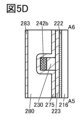
- Fig. 1A is a plan view showing an example of a semiconductor device
- Fig. 1B to Fig. 1D are cross-sectional views showing an example of a semiconductor device
- Fig. 1E is a schematic perspective view showing an example of a semiconductor device.
- 2A and 2B are cross-sectional views showing an example of a semiconductor device.
- 3A and 3B are cross-sectional views showing an example of a semiconductor device.
- Fig. 4A is a plan view showing an example of a semiconductor device
- Figs. 4B to 4D are cross-sectional views showing an example of the semiconductor device.
- Fig. 5A is a plan view showing an example of a semiconductor device
- Figs. 5B to 5D are cross-sectional views showing an example of the semiconductor device.
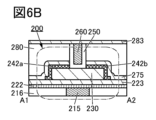
- Fig. 6A is a plan view showing an example of a semiconductor device
- Figs. 6B to 6D are cross-sectional views showing an example of the semiconductor device
- Fig. 7A is a plan view showing an example of a semiconductor device
- Figs. 7B to 7D are cross-sectional views showing an example of the semiconductor device
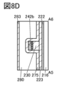
- Fig. 8A is a plan view showing an example of a semiconductor device
- Figs. 8B to 8D are cross-sectional views showing an example of the semiconductor device.
- 9A is a plan view showing an example of a semiconductor device
- FIGS. 9B to 9D are cross-sectional views showing an example of the semiconductor device
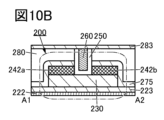
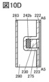
- Fig. 10A is a plan view showing an example of a semiconductor device, and Figs.
- FIG. 10B to 10D are cross-sectional views showing an example of the semiconductor device.
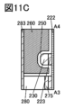
- Fig. 11A is a plan view showing an example of a semiconductor device, and Figs. 11B to 11D are cross-sectional views showing an example of the semiconductor device.
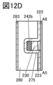
- Fig. 12A is a plan view showing an example of a semiconductor device, and Figs. 12B to 12D are cross-sectional views showing an example of the semiconductor device.
- Fig. 13A is a plan view showing an example of a semiconductor device, and Figs. 13B to 13D are cross-sectional views showing an example of the semiconductor device.
- Fig. 14A is a plan view showing an example of a semiconductor device, Fig. 14B to Fig.
- FIG. 14D are cross-sectional views showing an example of a semiconductor device
- Fig. 14E is a schematic perspective view showing an example of a semiconductor device
- FIG. 15 is a cross-sectional view showing an example of a semiconductor device.
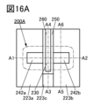
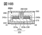
- Fig. 16A is a plan view showing an example of a semiconductor device
- Figs. 16B to 16D are cross-sectional views showing an example of the semiconductor device.
- Fig. 17A is a plan view showing an example of a semiconductor device
- Figs. 17B to 17D are cross-sectional views showing an example of the semiconductor device.
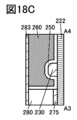
- Fig. 18A is a plan view showing an example of a semiconductor device
- Figs. 18B to 18D are cross-sectional views showing an example of the semiconductor device.
- Fig. 18A is a plan view showing an example of a semiconductor device
- Figs. 18B to 18D are cross-sectional views showing an example of the semiconductor device.
- Fig. 18A is a plan view showing
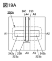
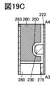
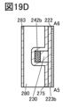
- FIG. 19A is a plan view showing an example of a semiconductor device
- Figs. 19B to 19D are cross-sectional views showing an example of the semiconductor device
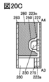
- Fig. 20A is a plan view showing an example of a semiconductor device
- Fig. 20B to Fig. 20D are cross-sectional views showing an example of the semiconductor device
- Fig. 21A is a plan view showing an example of a semiconductor device
- Fig. 21B to Fig. 21D are cross-sectional views showing an example of the semiconductor device
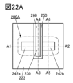
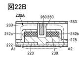
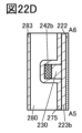
- Fig. 22A is a plan view showing an example of a semiconductor device
- Fig. 22B to Fig. 22D are cross-sectional views showing an example of the semiconductor device.
- Fig. 22A is a plan view showing an example of a semiconductor device
- Fig. 22B to Fig. 22D are cross-sectional views showing an example of the semiconductor device.
- Fig. 22A is a plan view showing an example of a semiconductor device
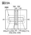
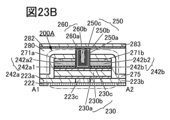
- FIG. 23A is a plan view showing an example of a semiconductor device
- Fig. 23B to Fig. 23D are cross-sectional views showing an example of the semiconductor device
- Fig. 24A is a plan view showing an example of a semiconductor device
- Fig. 24B to Fig. 24D are cross-sectional views showing an example of the semiconductor device
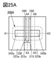
- Fig. 25A is a plan view showing an example of a semiconductor device
- Fig. 25B to Fig. 25D are cross-sectional views showing an example of the semiconductor device
- Fig. 26A is a plan view showing an example of a semiconductor device
- Fig. 26B to Fig. 26D are cross-sectional views showing an example of the semiconductor device.
- Fig. 26A is a plan view showing an example of a semiconductor device
- Fig. 26B to Fig. 26D are cross-sectional views showing an example of the semiconductor device.
- Fig. 26A is a plan view showing an example of a semiconductor device
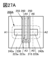
- FIG. 27A is a plan view showing an example of a semiconductor device
- Fig. 27B to Fig. 27D are cross-sectional views showing an example of the semiconductor device
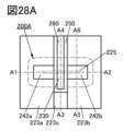
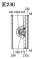
- Fig. 28A is a plan view showing an example of a semiconductor device
- Fig. 28B to Fig. 28D are cross-sectional views showing an example of the semiconductor device
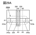
- Fig. 29A is a plan view showing an example of a semiconductor device
- Fig. 29B to Fig. 29D are cross-sectional views showing an example of the semiconductor device
- Fig. 30A is a plan view showing an example of a semiconductor device
- Fig. 30B to Fig. 30D are cross-sectional views showing an example of the semiconductor device.
- Fig. 30A is a plan view showing an example of a semiconductor device
- Fig. 30B to Fig. 30D are cross-sectional views showing an example of the semiconductor device.
- Fig. 30A is a plan view showing an example of a semiconductor device
- FIG. 31A is a plan view showing an example of a semiconductor device
- Fig. 31B to Fig. 31D are cross-sectional views showing an example of the semiconductor device
- Fig. 32A is a plan view showing an example of a semiconductor device
- Fig. 32B to Fig. 32D are cross-sectional views showing an example of the semiconductor device
- Fig. 33A is a plan view showing an example of a semiconductor device
- Fig. 33B to Fig. 33D are cross-sectional views showing an example of the semiconductor device
- 34A and 34B are cross-sectional views showing an example of a semiconductor device
- 35A and 35B are cross-sectional views showing an example of a semiconductor device.
- Fig. 31B to Fig. 31D are cross-sectional views showing an example of the semiconductor device.
- Fig. 32A is a plan view showing an example of a semiconductor device
- Fig. 32B to Fig. 32D are cross-sectional views showing an example of the semiconductor device
- FIG. 36A is a plan view showing an example of a semiconductor device
- Fig. 36B to Fig. 36D are cross-sectional views showing an example of the semiconductor device
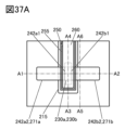
- Fig. 37A is a plan view showing an example of a semiconductor device
- Fig. 37B to Fig. 37D are cross-sectional views showing an example of the semiconductor device
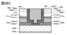
- 38A to 38C are cross-sectional views showing an example of a semiconductor device
- 39A to 39C are cross-sectional views showing an example of a semiconductor device
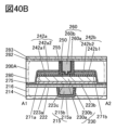
- Fig. 40A is a plan view showing an example of a semiconductor device
- Fig. 40B to Fig. 40D are cross-sectional views showing an example of the semiconductor device.
- Fig. 40A is a plan view showing an example of a semiconductor device
- Fig. 40B to Fig. 40D are cross-sectional views showing an example of the semiconductor device.
- Fig. 40A is a plan view showing an example of a semiconductor device
- FIG. 41A is a plan view showing an example of a semiconductor device
- Fig. 41B to Fig. 41D are cross-sectional views showing an example of the semiconductor device.
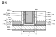
- FIG. 42 is a cross-sectional view showing an example of a semiconductor device.
- 43A to 43D are cross-sectional views showing an example of a semiconductor device.
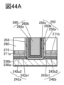
- 44A to 44C are cross-sectional views showing an example of a semiconductor device.
- Fig. 45A is a plan view showing an example of a semiconductor device, and Fig. 45B to Fig. 45D are cross-sectional views showing an example of the semiconductor device.
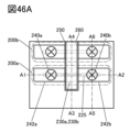
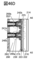
- Fig. 46A is a plan view showing an example of a semiconductor device
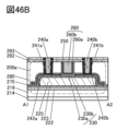
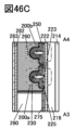
- Fig. 46B to Fig. 46D are cross-sectional views showing an example of the semiconductor device.
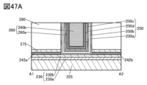
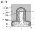
- FIG. 47A and 47B are cross-sectional views showing an example of a semiconductor device.
- 48A to 48C are cross-sectional views showing an example of a semiconductor device.
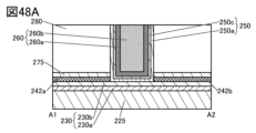
- 49A to 49C are cross-sectional views showing an example of a semiconductor device.
- Fig. 50A is a plan view showing an example of a semiconductor device
- Fig. 50B to Fig. 50D are cross-sectional views showing an example of the semiconductor device.
- FIG. 51 is a block diagram showing an example of a storage device.
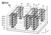
- 52A and 52B are a schematic diagram and a circuit diagram showing an example of a memory device.
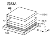
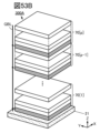
- 53A and 53B are schematic diagrams showing an example of a storage device.
- FIG. 54 is a circuit diagram showing an example of a memory device.
- 55A and 55B are cross-sectional views showing an example of a memory device.
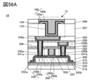
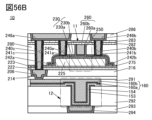
- 56A and 56B are cross-sectional views showing an example of a memory device.
- FIG. 57 is a cross-sectional view showing an example of a memory device.
- 58A and 58B are diagrams showing an example of a semiconductor device.
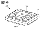
- 59A and 59B are diagrams showing an example of an electronic component.
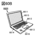
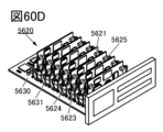
- 60A and 60B are diagrams showing an example of an electronic device, and
- FIGS. 60C to 60E are diagrams showing an example of a mainframe computer.
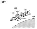
- FIG. 61 is a diagram showing an example of space equipment.
- FIG. 62 is a diagram illustrating an example of a storage system applicable to a data center.
- FIG. 63 is a diagram for explaining the laminated structure of the laminated film.
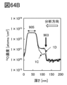
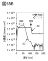
- 64A and 64B show the results of SIMS analysis of the prepared sample.
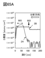
- 65A to 65C show the results of SIMS analysis of the prepared sample.
- top views also called “top views”
- perspective views some components may be omitted from the illustration. Also, some hidden lines may be omitted from the illustration.
- ordinal numbers “first” and “second” are used for convenience and do not limit the number of components or the order of the components (e.g., the order of processes or the order of stacking). Furthermore, an ordinal number attached to a component in one place in this specification may not match an ordinal number attached to the same component in another place in this specification or in the claims.
- film and “layer” may be interchangeable depending on the circumstances.
- conductive layer may be interchangeable with the term “conductive film”.
- insulating film may be interchangeable with the term “insulating layer”.
- conductor may be interchangeable with the term “conductive layer” or the term “conductive film” depending on the circumstances.
- insulating material may be interchangeable with the term “insulating layer” or the term “insulating film” depending on the circumstances.
- parallel refers to a state in which two straight lines are arranged at an angle of -10 degrees or more and 10 degrees or less. Therefore, it also includes cases where the angle is -5 degrees or more and 5 degrees or less.
- approximately parallel refers to a state in which two straight lines are arranged at an angle of -30 degrees or more and 30 degrees or less.
- Perfect refers to a state in which two straight lines are arranged at an angle of 80 degrees or more and 100 degrees or less. Therefore, it also includes cases where the angle is 85 degrees or more and 95 degrees or less.
- approximately perpendicular refers to a state in which two straight lines are arranged at an angle of 60 degrees or more and 120 degrees or less.
- Openings include, for example, grooves and slits. Also, the area in which an opening is formed may be referred to as an opening.
- the sidewalls of the insulator at the opening in the insulator are shown as being perpendicular or approximately perpendicular to the substrate surface or the surface on which the insulator is formed, but they may also be tapered.
- a tapered shape refers to a shape in which at least a portion of the side of the structure is inclined with respect to the substrate surface or the surface on which the structure is to be formed.
- the taper angle there is a region in which the angle between the inclined side and the substrate surface or the surface on which the structure is to be formed (hereinafter, sometimes referred to as the taper angle) is less than 90°.
- the side of the structure and the substrate surface do not necessarily need to be completely flat, and may be approximately planar with a slight curvature, or approximately planar with fine irregularities.
- “same height” refers to a configuration in which the heights from a reference surface (for example, a flat surface such as a substrate surface) are equal in cross-sectional view.
- a planarization process typically a CMP process
- the surfaces treated in the CMP process have a configuration in which the heights from the reference surface are equal.
- the heights of multiple layers may differ depending on the processing device, processing method, or material of the surface treated in the CMP process. In this specification, this case is also treated as "same height”.
- first layer and a second layer when there are two layers (here, a first layer and a second layer) with different heights relative to the reference surface, and the difference in height between the top surface of the first layer and the top surface of the second layer is 20 nm or less, this is also referred to as "same height”.
- side edges coincide means that at least a portion of the contours of the stacked layers overlap when viewed in a plane. For example, this includes cases where the upper and lower layers are processed using the same mask pattern, or where a portion of the mask pattern is the same. However, strictly speaking, the contours may not overlap, and the contour of the upper layer may be located inside the contour of the lower layer, or the contour of the upper layer may be located outside the contour of the lower layer, in which case it is also referred to as "side edges coincide”.
- the first film thickness and the second film thickness being the same means that the absolute value of the difference between the first film thickness and the second film thickness divided by the first film thickness is 0.1 or less. Alternatively, it means that the absolute value of the difference between the first film thickness and the second film thickness divided by the second film thickness is 0.1 or less.
- distance A and distance B are the same means that the absolute value of the difference between distance A and distance B divided by distance A is 0.1 or less. Or, the absolute value of the difference between distance A and distance B divided by distance B is 0.1 or less.
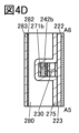
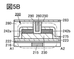
- the semiconductor device according to one embodiment of the present invention includes a transistor.
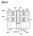
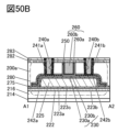
- a in each figure shows a plan view of the semiconductor device.
- B in each figure is a cross-sectional view corresponding to the portion indicated by the dashed line A1-A2 in A of each figure, and is also a cross-sectional view in the channel length direction of the transistor.
- C in each figure is a cross-sectional view corresponding to the portion indicated by the dashed line A3-A4 in A of each figure, and is also a cross-sectional view in the channel width direction of the transistor.
- D in each figure is a cross-sectional view corresponding to the portion indicated by the dashed line A5-A6 in A of each figure. In the plan view of A in each figure, some elements are omitted to clarify the figure.
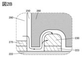
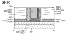
- 1A to 1D are plan views and cross-sectional views of a semiconductor device including a transistor 200.
- the semiconductor device shown in Figures 1A to 1D has an insulator 222 on a substrate (not shown), a transistor 200 on the insulator 222, an insulator 280 on the transistor 200, and an insulator 283 on the insulator 280.
- the insulators 222, 280, and 283 function as interlayer insulating films.
- the transistor 200 has an insulator 223 on the insulator 222, an oxide semiconductor 230 on the insulator 223, a conductor 242a and a conductor 242b on the oxide semiconductor 230, an insulator 275 on the insulator 223, the conductor 242a, and the conductor 242b, an insulator 250 on the oxide semiconductor 230, and a conductor 260 located on the insulator 250 and overlapping with a portion of the oxide semiconductor 230.
- the conductor 260 functions as a gate electrode of the transistor 200.
- the insulator 250 functions as a gate insulator of the transistor 200.
- the conductor 242a functions as one of the source electrode and drain electrode of the transistor 200, and the conductor 242b functions as the other of the source electrode and drain electrode of the transistor 200.
- At least a part of the region of the oxide semiconductor 230 that overlaps with the conductor 260 functions as a channel formation region of the transistor 200.
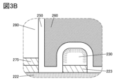
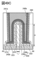
- FIG. 1E shows a schematic perspective view of the semiconductor device.
- insulator 222, insulator 223, oxide semiconductor 230, conductor 242b, insulator 250, conductor 260, insulator 275, and a portion of the surrounding area are shown cut away.
- FIG. 1E only the outlines of some components (e.g., insulator 280 and insulator 283) are shown by dashed lines.
- the oxide semiconductor 230 is provided in contact with the upper surface of the insulator 223.
- the conductor 242a and the conductor 242b are provided in contact with the upper surface of the oxide semiconductor 230.
- the insulator 275 is disposed on the insulator 223, the oxide semiconductor 230, the conductor 242a, and the conductor 242b. Specifically, the insulator 275 is provided in contact with the upper surface of the insulator 223, the side surface of the oxide semiconductor 230, the upper surface and side surface of the conductor 242a, and the upper surface and side surface of the conductor 242b.
- Insulator 280 is provided in contact with the upper surface of insulator 275.
- Each of the insulators 280 and 275 has an opening that reaches the oxide semiconductor 230.
- the insulator 223 also has an opening in a region of the opening that does not overlap with the oxide semiconductor 230.
- the opening in the insulator 280 is referred to as a first opening
- the opening in the insulator 275 is referred to as a second opening
- the opening in the insulator 223 is referred to as a third opening.
- the first opening, the second opening, and the third opening are collectively referred to as opening 290.
- the insulator 250 and the conductor 260 are provided inside the opening 290. That is, at least a portion of each of the insulator 250 and the conductor 260 is provided inside the first opening, the second opening, and the third opening. In addition, the insulator 250 and the conductor 260 are provided between the conductor 242a and the conductor 242b in the channel length direction of the transistor 200.
- Insulator 250 contacts the side of insulator 280 and the side of insulator 275 at opening 290. In addition, insulator 250 contacts the side of conductor 242a facing conductor 260 and the side of conductor 242b facing conductor 260. As shown in FIG. 1C, insulator 250 contacts the top and side of oxide semiconductor 230, the side of insulator 223, and the top of insulator 222 at opening 290.
- the conductor 260 is formed in a self-aligned manner so as to fill the opening 290.
- the conductor 260 can be reliably positioned in the region between the conductor 242a and the conductor 242b without alignment.
- the height of the upper surface of the conductor 260 coincides with the height of the insulator 250 and the insulator 280.
- the sidewall of the opening 290 is perpendicular or approximately perpendicular to the surface on which the oxide semiconductor 230 is to be formed, but this is not limited to this embodiment.
- the bottom surface of the opening 290 may be U-shaped with a gentle curve.
- the sidewall of the opening 290 may be tapered.
- the sidewall of the opening 290 corresponds to the side surface of the insulator 280 in the opening 290, the side surface of the insulator 275 in the opening 290, and the side surface of the insulator 223 in the opening 290.
- Insulator 283 is disposed on insulator 280, on insulator 250, and on conductor 260.
- the transistor 200 preferably uses a metal oxide (hereinafter also referred to as an oxide semiconductor) that functions as a semiconductor for the oxide semiconductor 230 including the channel formation region.
- a metal oxide described in the [Metal Oxide] section described later can be used in a single layer or a stacked layer.
- the composition close thereto includes a range of ⁇ 30% of the desired atomic ratio. It is also preferable to use gallium as the element M.
- the oxide semiconductor 230 may not contain the element M.
- the metal oxide used as the oxide semiconductor 230 may be an In-Zn oxide.
- the composition of the metal oxide used in the oxide semiconductor 230 can be analyzed using, for example, energy dispersive X-ray spectroscopy (EDX), X-ray photoelectron spectroscopy (XPS), inductively coupled plasma mass spectrometry (ICP-MS), or inductively coupled plasma-atomic emission spectrometry (ICP-AES).
- EDX energy dispersive X-ray spectroscopy
- XPS X-ray photoelectron spectroscopy
- ICP-MS inductively coupled plasma mass spectrometry
- ICP-AES inductively coupled plasma-atomic emission spectrometry
- a combination of these techniques may be used for the analysis.
- the actual content may differ from the content obtained by analysis due to the influence of analytical accuracy. For example, if the content of element M is low, the content of element M obtained by analysis may be lower than the actual content.
- the metal oxide can be formed preferably by sputtering or atomic layer deposition (ALD).
- ALD atomic layer deposition
- the composition of the formed metal oxide may differ from the composition of the sputtering target.
- the zinc content in the formed metal oxide may decrease to about 50% compared to the sputtering target.
- Examples of the ALD method include the Thermal ALD method, in which the reaction between the precursor and reactant is carried out using only thermal energy, and the Plasma Enhanced ALD (PEALD) method, in which a plasma-excited reactant is used.
- Thermal ALD method in which the reaction between the precursor and reactant is carried out using only thermal energy
- PEALD Plasma Enhanced ALD
- the ALD method can deposit atoms one layer at a time, which has the following advantages: extremely thin films can be formed; films can be formed on structures with high aspect ratios or surfaces with large steps; films can be formed with few defects such as pinholes; films can be formed with excellent coverage; and films can be formed at low temperatures.
- the PEALD method may be preferable in some cases because it uses plasma, which allows films to be formed at lower temperatures.
- some precursors used in the ALD method contain elements such as carbon or chlorine.
- films formed by the ALD method may contain more elements such as carbon or chlorine than films formed by other film formation methods. Note that the amount of these elements can be quantified using XPS or secondary ion mass spectrometry (SIMS).
- the metal oxide film formation method uses the ALD method, but because it employs a high substrate temperature condition during film formation and/or performs an impurity removal process, the amount of carbon and chlorine contained in the film may be less than when the ALD method is used without applying these conditions.
- the ALD method is a film formation method in which a film is formed by a reaction on the surface of a workpiece, unlike a film formation method in which particles released from a target are deposited. Therefore, it is a film formation method that is not easily affected by the shape of the workpiece and has good step coverage.
- the ALD method has excellent step coverage and excellent thickness uniformity, making it suitable for coating the surface of an opening with a high aspect ratio.
- the ALD method since the ALD method has a relatively slow film formation speed, it may be preferable to use it in combination with other film formation methods such as a sputtering method or a CVD method, which have a fast film formation speed.
- the metal oxide has a layered structure of a first metal oxide and a second metal oxide
- a method of forming a film of the first metal oxide using a sputtering method and forming a film of the second metal oxide on the first metal oxide using an ALD method can be mentioned.
- the first metal oxide has a crystalline portion
- the second metal oxide may grow as a crystal using the crystalline portion as a nucleus.
- the ALD method can control the composition of the resulting film by adjusting the amount of raw material gas introduced.
- the ALD method can form a film of any composition by adjusting the amount of raw material gas introduced, the number of times it is introduced (also called the number of pulses), the time required for one pulse (also called the pulse time), and the like.
- the ALD method can form a film whose composition changes continuously by changing the raw material gas while forming the film.
- the time required for film formation can be shortened compared to forming a film using multiple film formation chambers because no time is required for transportation and pressure adjustment. Therefore, it may be possible to increase the productivity of memory devices.
- FIG. 2A shows an enlarged view of the channel formation region and its vicinity in FIG. 1B
- FIG. 2B shows an enlarged view of the channel formation region and its vicinity in FIG. 1C
- the oxide semiconductor 230 has a region 231a that overlaps with the conductor 242a, a region 231b that overlaps with the conductor 242b, and a region 231c located between the regions 231a and 231b.
- the oxide semiconductor 230 has the region 231c, and the regions 231a and 231b that are provided so as to sandwich the region 231c.
- Region 231c at least partially overlaps with conductor 260.
- Region 231c also has an area that overlaps with opening 290.
- region 231c has an area that overlaps with a first opening provided in insulator 280 and a second opening provided in insulator 275.
- insulator 280 has a first opening in the area that overlaps with region 231c
- insulator 275 has a second opening in the area that overlaps with region 231c.
- Region 231c functions as a channel formation region of transistor 200.
- Region 231a functions as one of the source region and drain region of transistor 200, and region 231b functions as the other of the source region and drain region of transistor 200.
- the channel formation region of the transistor is a high-resistance region with a low carrier concentration. Therefore, the channel formation region of the transistor can be said to be i-type (intrinsic) or substantially i-type. Furthermore, the source and drain regions of the transistor are regions with a high carrier concentration and low resistance (low-resistance n-type regions) compared to the channel formation region.
- the electrical characteristics are likely to fluctuate and the reliability may be reduced.
- hydrogen near the oxygen vacancies may form defects in which hydrogen is inserted into the oxygen vacancies (hereinafter, may be referred to as VOH ), and may generate electrons that serve as carriers.
- VOH oxygen vacancies
- the transistor is likely to have normally-on characteristics (characteristics in which a channel exists and a current flows through the transistor even when no voltage is applied to the gate electrode). Therefore, it is preferable that the channel formation region in the oxide semiconductor has fewer oxygen vacancies, fewer VOH , or a lower concentration of impurities such as hydrogen, nitrogen, and metal elements than the source and drain regions.
- the source and drain regions in the oxide semiconductor preferably have more oxygen vacancies, more VOH , or a higher concentration of impurities such as hydrogen, nitrogen, or metal elements than the channel formation region.
- an insulator containing oxygen that is desorbed by heating (hereinafter may be referred to as excess oxygen) is preferably provided near the oxide semiconductor.
- excess oxygen oxygen can be supplied from the insulator to a channel formation region of the oxide semiconductor, and oxygen vacancies and VOH can be reduced.
- the on-state current or the field-effect mobility of the transistor may decrease.
- the amount of oxygen supplied to the source and drain regions varies within the substrate plane, which causes variation in the electrical characteristics of the transistor. In other words, it is preferable to prevent an excessive amount of oxygen from being supplied to the source and drain regions of the oxide semiconductor.
- insulator 250 is in contact with the top surface and side surface of region 231c, and insulator 223 is in contact with the bottom surface of oxide semiconductor 230.
- an insulator that is easily permeable to oxygen may be used as insulator 250.
- oxygen contained in the insulator containing excess oxygen can be supplied to region 231c via insulator 250.
- an example of an insulator provided near insulator 250 is insulator 280.
- an insulator containing excess oxygen is used as the insulator 280, it is preferable to provide a barrier insulator against oxygen between the insulator 280 and the regions 231a and 231b. With such a structure, the amount of oxygen supplied to the source region or drain region of the oxide semiconductor 230 can be reduced.
- an insulator 275 is provided between the insulator 280 and the regions 231a and 231b.
- the insulators 223 and 275 it is preferable to use, for example, silicon nitride, more preferably silicon nitride formed by the ALD method, and even more preferably silicon nitride formed by the PEALD method.
- the insulators 223 and 275 each contain silicon and nitrogen.
- the ALD method has excellent step coverage and excellent thickness uniformity, and is therefore suitable for forming thin films and coating surfaces with high aspect ratios.
- a silicon nitride film is formed by using the PEALD method
- a precursor containing a halogen such as fluorine, chlorine, bromine, iodine, etc.
- a plasma treatment is performed in an atmosphere containing a nitriding agent such as N2 , N2O , NH3 , NO, NO2 , or N2O2 , thereby forming a high-quality silicon nitride film.
- insulator 275 is configured to contact a portion of the upper surface of insulator 223. At this time, regions 231a and 231b are surrounded by insulator 223 and insulator 275, respectively. Furthermore, regions 231a and 231b are in contact with insulator 223 and insulator 275, respectively.
- the insulator 250 is configured to contact the side surface of the insulator 223 and a part of the upper surface of the insulator 222. At this time, the region 231c is surrounded by the insulator 223 and the insulator 250. The region 231c is also in contact with the insulator 223 and the insulator 250.
- a structure surrounded by a first insulator and a second insulator refers to a configuration in which the first insulator is located on at least a portion of the top surface and at least a portion of the side surface of the structure, and the second insulator is located on at least a portion of the bottom surface of the structure. Or, it refers to a configuration in which the first insulator is located on at least a portion of the top surface of the structure, and the second insulator is located on at least a portion of the side surface and at least a portion of the bottom surface of the structure.
- another structure may be provided between the first insulator and the structure.
- another structure may be provided between the second insulator and the structure.
- microwave treatment in an atmosphere containing oxygen with the conductor 242a and the conductor 242b provided on the oxide semiconductor 230.
- microwave processing refers to processing using a device with a power source that generates high-density plasma using microwaves.
- microwaves refer to electromagnetic waves with a frequency of 300 MHz or more and 300 GHz or less.
- Microwave processing can also be called microwave-excited high-density plasma processing.
- oxygen gas By performing microwave processing in an atmosphere containing oxygen, oxygen gas can be turned into plasma using microwaves or high frequency waves such as RF, and the oxygen plasma can be made to act. At this time, microwaves or high frequency waves such as RF can also be irradiated onto the region 231c.
- microwaves or high frequency waves such as RF can also be irradiated onto the region 231c.
- the VOH in the region 231c can be split into oxygen vacancies ( V0 ) and hydrogen (H), the hydrogen can be removed from the region 231c, and the oxygen vacancies can be compensated for with oxygen. Therefore, the hydrogen concentration, oxygen vacancies, and VOH in the region 231c can be reduced, and the carrier concentration can be lowered.
- the effects of microwaves, high frequency waves such as RF, oxygen plasma, and the like are shielded by the conductors 242a and 242b and do not reach the regions 231a and 231b. Furthermore, the effects of oxygen plasma can be reduced by the insulators 275 and 280 provided to cover the oxide semiconductor 230, the conductor 242a, and the conductor 242b. As a result, reduction in VOH and supply of an excessive amount of oxygen are not generated in the regions 231a and 231b during microwave treatment, and thus a decrease in carrier concentration can be prevented.
- the insulating film that becomes the insulator 250 it is preferable to perform microwave treatment in an atmosphere containing oxygen.
- microwave treatment in an atmosphere containing oxygen through the insulator 250 in this manner, oxygen can be efficiently injected into the region 231c.
- the insulator 250 by arranging the insulator 250 so that it is in contact with the side of the conductor 242a, the side of the conductor 242b, and the surface of the region 231c, it is possible to prevent the injection of more oxygen than necessary into the region 231c, and to prevent oxidation of the side of the conductor 242a and the conductor 242b.
- the oxygen injected into region 231c can take various forms, such as oxygen atoms, oxygen molecules, oxygen ions (charged oxygen atoms or oxygen molecules), and oxygen radicals (oxygen atoms, oxygen molecules, or oxygen ions with an unpaired electron).
- the oxygen injected into region 231c may take one or more of the above forms, and is particularly preferably oxygen radicals.
- the film quality of insulator 250 can be improved, thereby improving the reliability of transistor 200.
- oxygen vacancies and VOH can be selectively removed from the region 231c functioning as a channel formation region, making the region 231c i-type or substantially i-type. Furthermore, excessive supply of oxygen to the regions 231a and 231b functioning as source and drain regions can be suppressed, and the state of the n-type regions before the microwave treatment can be maintained. This can suppress fluctuations in the electrical characteristics of the transistor 200, and can suppress variations in the electrical characteristics of the transistor 200 within the substrate surface.
- oxygen can be efficiently supplied to region 231c, and the channel formation region can be made into an i-type region. Furthermore, since the amount of oxygen supplied to regions 231a and 231b is smaller than that to region 231c, it is possible to prevent a decrease in the carrier concentration in the source and drain regions.
- a barrier insulator against hydrogen as described in the [Insulator] section below, for the insulator 223 and the insulator 275.
- Silicon nitride has barrier properties against hydrogen and is therefore suitable for the insulator 275 and the insulator 223.
- Silicon nitride which can be used as insulator 223 and insulator 275, has a barrier property against oxygen if the film thickness is, for example, 1.0 nm or more, and has a high barrier property against oxygen if the film thickness is, for example, 1.4 nm or more. Silicon nitride also has a barrier property against hydrogen if the film thickness is, for example, 2.5 nm or more, and has a high barrier property against hydrogen if the film thickness is, for example, 3.3 nm or more.
- the thickness of the insulator 223 is preferably 1.0 nm or more, and more preferably 1.4 nm or more.
- the upper limit of the thickness of the insulator 223 is not particularly limited, but from the viewpoint of miniaturization or high integration of the semiconductor device and improvement of the productivity of the semiconductor device, it is preferably 20 nm or less, 10 nm or less, or 5.0 nm or less. Therefore, the insulator 223 preferably has a region with a thickness of 1.0 nm or more and 10 nm or less, and more preferably has a region with a thickness of 1.0 nm or more and 5.0 nm or less. Furthermore, the insulator 223 preferably has a region with a thickness of 1.4 nm or more and 10 nm or less, and more preferably has a region with a thickness of 1.4 nm or more and 5.0 nm or less.
- insulator 223 and insulator 275 are formed using the same insulating material, a third opening is formed in insulator 223 when insulator 275 is etched to form the second opening. At this time, insulator 250 contacts insulator 222 at the third opening (see FIG. 1C).
- Insulators that can be used as the insulators 223 and 275 are not limited to silicon nitride.
- silicon nitride aluminum oxide or hafnium oxide may be used.
- each of the insulators 223 and 275 may have a laminated structure.
- the insulator 223 may have a laminated structure of silicon nitride and aluminum oxide on the silicon nitride, and the insulator 275 may have a laminated structure of aluminum oxide and silicon nitride on the aluminum oxide.
- the insulator 223 may have a laminated structure of aluminum oxide and silicon nitride on the aluminum oxide, and the insulator 275 may have a laminated structure of silicon nitride and aluminum oxide on the silicon nitride.
- the oxide semiconductor 230 preferably has crystallinity.
- oxide semiconductors having crystallinity include CAAC-OS (c-axis aligned crystalline oxide semiconductor), nc-OS (nanocrystalline oxide semiconductor), polycrystalline oxide semiconductor, and single-crystalline oxide semiconductor. It is preferable to use CAAC-OS or nc-OS as the oxide semiconductor 230, and it is particularly preferable to use CAAC-OS.
- CAAC-OS is a metal oxide that has a highly crystalline and dense structure and has few impurities and defects (e.g., oxygen vacancies).
- a temperature e.g. 400°C or higher and 600°C or lower
- the CAAC-OS can be made to have a more crystalline and dense structure. In this way, the density of the CAAC-OS can be further increased, thereby further reducing the diffusion of impurities or oxygen in the CAAC-OS.
- the oxide semiconductor 230 Furthermore, by using a crystalline oxide such as CAAC-OS as the oxide semiconductor 230, it is possible to suppress the extraction of oxygen from the oxide semiconductor 230 by the source electrode or the drain electrode. As a result, even when heat treatment is performed, it is possible to suppress the extraction of oxygen from the oxide semiconductor 230, and therefore the transistor 200 is stable against high temperatures (so-called thermal budget) in the manufacturing process.
- a crystalline oxide such as CAAC-OS
- FIG. 3A and FIG. 3B enlarged views of the channel formation region and its vicinity in FIG. 1C are shown in FIG. 3A and FIG. 3B.
- the CAAC-OS has multiple crystals, and each of the multiple crystals has a crystal structure in which multiple layers are stacked.
- the c-axis of the crystals of the CAAC-OS used as the oxide semiconductor 230 is preferably oriented in a direction perpendicular to the channel length direction.
- the c-axis of the crystals of the region 231c that functions as a channel formation region is preferably oriented in a direction perpendicular to the channel length direction.
- the channel formation region is electrically surrounded by the electric field of the conductor 260. Therefore, the side surface of region 231c also functions as a channel formation region. Therefore, it is preferable that the c-axis of the crystals in the vicinity of the side surface of region 231c facing the insulator 250 is also oriented in a direction perpendicular to the channel length direction. In other words, it is preferable that region 231c has crystals in the side surface near the insulator 250, and that the c-axis of the crystals is oriented in a direction perpendicular to the channel length direction.
- One example of the above-mentioned structure is a structure in which a layer contained in the crystal extends parallel or approximately parallel to the surface on which the oxide semiconductor 230 is formed (see FIG. 3A).
- the above-mentioned crystals are formed during the formation of the oxide semiconductor film that becomes the oxide semiconductor 230, so that the oxide semiconductor 230 having the crystals can be formed.
- the oxide semiconductor film is preferably formed while heating the substrate. Note that an oxide semiconductor film formed by a sputtering method is likely to have crystallinity, and is therefore suitable for forming the oxide semiconductor 230 having the crystals.
- the oxide semiconductor 230 having the above-mentioned crystals can be formed by processing the oxide semiconductor film to be the oxide semiconductor 230 into an island shape and then performing a process selected from plasma processing, microwave processing, and heat treatment, for example, to form the oxide semiconductor 230 into a crystal structure.
- the oxide semiconductor film is formed by the ALD method, the crystallinity of the oxide semiconductor film may be low due to remaining impurities contained in the raw material such as a precursor. Therefore, by forming the oxide semiconductor film, processing it into an island shape, and then performing the above process, the impurity concentration of the oxide semiconductor 230 can be reduced, and crystal growth from the surface side of the oxide semiconductor 230 can be promoted.
- the method for forming the oxide semiconductor film that becomes the oxide semiconductor 230 is not particularly limited.
- the oxide semiconductor film can be formed using a CVD method, an MBE method, a PLD method, or the like.
- the ALD method may be used to form the structure shown in FIG. 3A, or the sputtering method may be used to form the structure shown in FIG. 3B.
- the crystallinity of the oxide semiconductor 230 can be analyzed, for example, by X-ray diffraction (XRD), a transmission electron microscope (TEM), or electron diffraction (ED). Alternatively, the analysis may be performed by combining a plurality of these techniques.
- XRD X-ray diffraction
- TEM transmission electron microscope
- ED electron diffraction
- the oxide semiconductor 230 is shown as a single layer, but the present invention is not limited to this.
- the oxide semiconductor 230 may have a laminated structure of multiple oxide layers with different chemical compositions.
- the oxide semiconductor 230 may have a structure in which multiple types of metal oxides selected from the metal oxides described above and those described in the [Metal Oxide] section below are appropriately laminated.
- the oxide semiconductor 230 may have a stacked structure of an oxide semiconductor 230a, an oxide semiconductor 230b on the oxide semiconductor 230a, and an oxide semiconductor 230c on the oxide semiconductor 230b.
- the atomic ratio of element M to In is preferably greater than the atomic ratio of element M to In in the metal oxide used for oxide semiconductor 230b.
- the insulator 223 may not be effective in suppressing the diffusion of hydrogen.
- the oxide semiconductor 230a between the insulator 223 and the oxide semiconductor 230b the diffusion of hydrogen from the substrate side to the oxide semiconductor 230b can be suppressed.
- the oxide semiconductor 230a may not be provided.
- the oxide semiconductor 230 may have a stacked structure of an oxide semiconductor 230b and an oxide semiconductor 230c on the oxide semiconductor 230b.
- the thickness of the insulator 223 is not limited to the above. Even if the thickness of the insulator 223 is 1.0 nm or more or 1.4 nm or more and 2.5 nm or less, the oxide semiconductor 230a may not be provided.
- the oxide semiconductor 230a may not be provided.
- the oxide semiconductor film that becomes the oxide semiconductor 230b is formed using an ALD method or a CVD method
- the oxide semiconductor 230a may not be provided.
- damage to the insulator 223 is reduced, and the diffusion of elements contained in the insulator 223 into the oxide semiconductor film can be suppressed.
- the conductivity of the material used for the oxide semiconductor 230b may differ from the conductivity of the material used for the oxide semiconductor 230a.
- the band gap of the material used for the oxide semiconductor 230b may differ from the band gap of the material used for the oxide semiconductor 230a.
- the conductivity of the material used for the oxide semiconductor 230b is preferably different from that of the material used for the oxide semiconductor 230c.
- a material having a higher conductivity than the oxide semiconductor 230c can be used for the oxide semiconductor 230b.
- a transistor with a large on-state current can be obtained.
- the oxide semiconductor 230b may be made of a material having a higher conductivity than the oxide semiconductor 230a. By using a material having a high conductivity for the oxide semiconductor 230b, a transistor having a large on-state current can be obtained.
- the atomic ratio of In to Zn in the oxide semiconductor 230b is preferably greater than the atomic ratio of In to Zn in the oxide semiconductor 230a.
- the atomic ratio of In to Zn in the oxide semiconductor 230b is preferably greater than the atomic ratio of In to Zn in the oxide semiconductor 230c.
- the film thickness of the oxide semiconductor 230b is preferably greater than the film thickness of the oxide semiconductor 230a and the film thickness of the oxide semiconductor 230c.
- the threshold voltage of the transistor 200 may shift, and the drain current (hereinafter also referred to as cutoff current) that flows when the gate voltage is 0 V may become large.
- the threshold voltage may become low. Therefore, it is preferable to use a material with lower conductivity than the oxide semiconductor 230b for the oxide semiconductor 230c.
- the threshold voltage can be increased, and the transistor can have a small cutoff current. Note that a small cutoff current may be referred to as a normally-off transistor.
- the oxide semiconductor 230b As described above, by using a material having a higher conductivity than the oxide semiconductor 230c as the oxide semiconductor 230b, a normally-off transistor with a large on-state current can be obtained. Therefore, a semiconductor device that achieves both low power consumption and high performance can be obtained.
- the carrier concentration of the oxide semiconductor 230b is preferably higher than that of the oxide semiconductor 230c.
- the conductivity is increased, and a transistor with a large on-state current can be obtained.
- the conductivity is decreased, and a normally-off transistor can be obtained.
- the oxide semiconductor 230b is made of a material having a higher conductivity than the oxide semiconductor 230c; however, one embodiment of the present invention is not limited to this.
- the oxide semiconductor 230b may be made of a material having a lower conductivity than the oxide semiconductor 230c.
- the carrier concentration of the oxide semiconductor 230b may be lower than the carrier concentration of the oxide semiconductor 230c.
- the band gap of the first metal oxide used in the oxide semiconductor 230b is preferably different from the band gap of the second metal oxide used in the oxide semiconductor 230c.
- the difference between the band gap of the first metal oxide and the band gap of the second metal oxide is preferably 0.1 eV or more, more preferably 0.2 eV or more, and even more preferably 0.3 eV or more.
- the band gap of the first metal oxide used in the oxide semiconductor 230b can be smaller than the band gap of the second metal oxide used in the oxide semiconductor 230c. With this configuration, a transistor with a large on-state current can be obtained. Furthermore, when the transistor 200 is an n-channel transistor, the threshold voltage can be increased, and the transistor can be a normally-off transistor.
- the band gap of the first metal oxide is smaller than the band gap of the second metal oxide, but one embodiment of the present invention is not limited to this.
- the band gap of the first metal oxide may be larger than the band gap of the second metal oxide.
- the oxide semiconductor 230c has a higher barrier property against oxygen than the oxide semiconductor 230b.
- the oxide semiconductor 230c By disposing the oxide semiconductor 230c between the conductor 242a and the oxide semiconductor 230b and between the conductor 242b and the oxide semiconductor 230b, it is possible to suppress the conductor 242a and the conductor 242b from being oxidized by the oxygen contained in the oxide semiconductor 230b, which would increase the resistivity and reduce the on-current. Therefore, it is possible to improve the electrical characteristics, field effect mobility, and reliability of the transistor 200.
- the oxide semiconductor 230c may not be provided.
- the oxide semiconductor 230 may have a stacked structure of the oxide semiconductor 230a and the oxide semiconductor 230b on the oxide semiconductor 230a.
- the insulators described in the section [Insulators] below can be used in a single layer or a multilayer.
- silicon oxide or silicon oxynitride can be used as the insulator 250. Silicon oxide and silicon oxynitride are preferred because they are stable against heat.
- insulator 250 a material with a high relative dielectric constant, so-called high-k material, described in the section [Insulator] below, may be used.
- high-k material a material with a high relative dielectric constant
- hafnium oxide or aluminum oxide may be used.
- the insulator 250 is provided in an opening formed in the insulator 280, etc., together with the conductor 260. In order to miniaturize the transistor 200, it is preferable that the thickness of the insulator 250 is thin.
- the thickness of the insulator 250 is preferably 0.5 nm or more and 15 nm or less, more preferably 0.5 nm or more and 12 nm or less, and even more preferably 0.5 nm or more and 10 nm or less. It is sufficient that at least a part of the insulator 250 has a region with the above-mentioned thickness.
- the concentration of impurities such as water and hydrogen in the insulator 250 is reduced. This can prevent impurities such as water and hydrogen from entering the channel formation region of the oxide semiconductor 230.
- Insulator 250 may have a laminated structure.
- insulator 250 may have a laminated structure of insulator 250a, insulator 250b on insulator 250a, and insulator 250c on insulator 250b.
- insulator 250b it is advisable to use an insulator that is applicable to insulator 250 described above.
- the insulator 250a is preferably an oxygen barrier insulator as described in the [Insulator] section below.
- the insulator 250a has a region in contact with the oxide semiconductor 230.
- the insulator 250a has a barrier property against oxygen, and thus can suppress oxygen from being released from the oxide semiconductor 230 when heat treatment or the like is performed. This can suppress the formation of oxygen vacancies in the oxide semiconductor 230. This can improve the electrical characteristics and reliability of the transistor 200.
- aluminum oxide can be used as the insulator 250a. In this case, the insulator 250a contains at least oxygen and aluminum.
- the insulator 250c is preferably a barrier insulator against hydrogen, as described in the [Insulator] section below. This can suppress the diffusion of impurities contained in the conductor 260 into the oxide semiconductor 230. Silicon nitride has high hydrogen barrier properties and is therefore suitable as the insulator 250c. In this case, the insulator 250c contains at least nitrogen and silicon.
- the insulator 250c may further have a barrier property against oxygen.
- the insulator 250c is provided between the insulator 250b and the conductor 260. This prevents the oxygen contained in the insulator 250b from diffusing into the conductor 260, and suppresses oxidation of the conductor 260. In addition, a decrease in the amount of oxygen supplied to the region 231c can be suppressed.
- an insulator may be provided between the insulator 250b and the insulator 250c.
- the insulator it is preferable to use an insulator having a function of capturing or fixing hydrogen, as described in the section [Insulator] below.
- the insulator hydrogen contained in the oxide semiconductor 230 can be captured or fixed more effectively.
- the hydrogen concentration in the oxide semiconductor 230 can be reduced.
- hafnium oxide may be used as the insulator.
- the insulator contains at least oxygen and hafnium.
- the insulator may have an amorphous structure.
- the thicknesses of the insulators 250a to 250c are preferably thin and within the aforementioned range.
- the thicknesses of the insulators 250a, 250b, the insulator having the function of capturing or fixing hydrogen, and the insulator 250c are 1 nm, 2 nm, 2 nm, and 1 nm, respectively.
- the films In order to make the film thickness of the insulators 250a to 250c as thin as described above, it is preferable to form the films using the ALD method. Also, in order to provide the insulators 250a to 250c inside the openings provided in the insulator 280, etc., it is preferable to form the films using the ALD method.
- Figures 4A to 4D show a configuration in which the insulator 250 has a three-layer stacked structure of insulators 250a to 250c, the present invention is not limited to this.
- the insulator 250 may have a two-layer or four or more layer stacked structure.
- each layer included in the insulator 250 may be appropriately selected from insulators 250a to 250c and insulators that have the function of capturing or fixing hydrogen.
- the insulator 280 functions as an interlayer film, it is preferable that it has a low dielectric constant. By using a material with a low dielectric constant as the interlayer film, the parasitic capacitance that occurs between wiring can be reduced.
- the insulator 280 a single layer or a multilayer of insulators containing a material with a low dielectric constant, as described in the [Insulator] section below, can be used. Silicon oxide and silicon oxynitride are preferable because they are thermally stable.
- the concentration of impurities such as water and hydrogen in the insulator 280 is reduced. This can suppress the intrusion of impurities such as water and hydrogen into the channel formation region of the oxide semiconductor 230.
- the insulator 283 is preferably a barrier insulator against hydrogen, as described in the [Insulator] section below. This can prevent hydrogen from diffusing from outside the transistor 200 to the oxide semiconductor 230 through the insulator 250. Silicon nitride and silicon nitride oxide each have the characteristics of releasing little impurities (e.g., water and hydrogen) from themselves and being less permeable to oxygen and hydrogen, and therefore can be suitably used for the insulator 283.
- impurities e.g., water and hydrogen
- the insulator 283 contains silicon and nitrogen.
- the sputtering method does not require the use of molecules containing hydrogen in the deposition gas, and therefore the hydrogen concentration in the insulator 283 can be reduced. Furthermore, by depositing the insulator 283 by sputtering, silicon nitride with high density can be formed.
- the film thickness of insulator 223 may be different from the film thickness of insulator 283.
- the film thickness of insulator 223 is smaller than the film thickness of insulator 283.
- Insulator 223 may have at least a portion of a region having a smaller film thickness than insulator 283.
- insulator 223 preferably has barrier properties against at least oxygen, and insulator 283 preferably has barrier properties against hydrogen. Therefore, insulator 223 may have a region having a smaller film thickness than insulator 283.
- the concentration of the impurity element in the insulator 223 may be different from the concentration of the impurity element in the insulator 283.
- the concentration of the impurity element in the insulator 223 may be higher than the concentration of the impurity element in the insulator 283.
- the impurity element is a halogen such as fluorine, chlorine, bromine, or iodine, hydrogen, or carbon.
- the insulator 223 is preferably formed by the ALD method, and the insulator 283 is preferably formed by the sputtering method. When an insulator is formed by the ALD method, impurities contained in the raw materials such as the precursor remain.
- the insulator formed by the ALD method tends to have a high concentration of the impurity element.
- the insulator formed by the ALD method tends to have a high concentration of the halogen.
- the concentration of the halogen in the insulator 223 may be higher than the concentration of the halogen in the insulator 283.
- the insulator formed using the ALD method tends to have high hydrogen and carbon concentrations. That is, the hydrogen concentration of the insulator 223 may be higher than the hydrogen concentration of the insulator 283.
- the carbon concentration of the insulator 223 may be higher than the carbon concentration of the insulator 283.
- the insulator 222 is preferably a barrier insulator against hydrogen, as described in the [Insulator] section below.
- the insulator 222 has a barrier property against hydrogen, the diffusion of hydrogen from below the insulator 222 to the oxide semiconductor 230 can be suppressed even if the thickness of the insulator 223 is thin.
- the insulator 222 is made of a metal oxide having an amorphous structure. With this structure, hydrogen contained in the channel formation region of the transistor 200 can be captured or fixed.
- the insulator 222 may have a barrier property against oxygen.
- the insulator 222 and the insulator 223 that have a barrier property against oxygen it is possible to prevent oxygen from being released from the oxide semiconductor 230.
- an insulator 222 that functions as an etching stopper film when etching insulator 223 to form the third opening.
- the insulator 222 may have a laminated structure.
- the insulator 222 may have a laminated structure of silicon nitride and hafnium oxide on the silicon nitride. With this configuration, it is possible to suppress the diffusion of hydrogen from below the insulator 222 to the oxide semiconductor 230.
- the conductor 260 may be a single layer or a multilayer of the conductors described in the section below titled "Conductor.”
- the conductor 260 may be a highly conductive material such as tungsten.
- the conductor 260 a conductive material that is resistant to oxidation, or a conductive material that has the function of suppressing the diffusion of oxygen.
- conductive materials include conductive materials that contain nitrogen (e.g., titanium nitride or tantalum nitride), and conductive materials that contain oxygen (e.g., ruthenium oxide).
- nitrogen e.g., titanium nitride or tantalum nitride
- oxygen e.g., ruthenium oxide
- the conductor 260 contains at least the metal and nitrogen. This makes it possible to suppress a decrease in the conductivity of the conductor 260.
- the conductor 260 may have a laminated structure.
- the conductor 260 may have a laminated structure of a conductor 260a and a conductor 260b on the conductor 260a.
- the conductor 260a is preferably made of a conductive material that has the function of suppressing the diffusion of oxygen. This can suppress the oxidation of the conductor 260b due to the oxygen contained in the insulator 280, etc., which leads to a decrease in conductivity.
- titanium nitride can be used as the conductor 260a.
- the conductor 260b is preferably made of a conductive material with high conductivity.
- tungsten can be used as the conductor 260b. By providing a layer containing tungsten in this manner, the conductivity of the conductor 260 can be improved, allowing it to function adequately as wiring.
- conductor 260 has a two-layer laminate structure of conductor 260a and conductor 260b
- the present invention is not limited to this.
- Conductor 260 may have a laminate structure of three or more layers.
- conductors 242a and 242b can be used as the conductors 242a and 242b, either in a single layer or in a multilayer configuration.
- the conductors 242a and 242b can be made of a highly conductive material, such as tungsten.
- the conductors 242a and 242b are made of a conductive material that is difficult to oxidize or that has a function of suppressing the diffusion of oxygen.
- a conductive material that is difficult to oxidize or that has a function of suppressing the diffusion of oxygen.
- titanium nitride or tantalum nitride can be used.
- each of the conductors 242a and 242b contains at least a metal and nitrogen. With this configuration, it is possible to suppress excessive oxidation of the conductors 242a and 242b by the oxide semiconductor 230.
- the conductor 242a and the conductor 242b are each shown as a single layer, but the present invention is not limited to this.
- the conductor 242a and the conductor 242b may each have a laminated structure.
- the conductor 242a may have a laminated structure of the conductor 242a1 and the conductor 242a2 on the conductor 242a1.
- the conductor 242b may have a laminated structure of the conductor 242b1 and the conductor 242b2 on the conductor 242b1.
- titanium nitride or tantalum nitride may be used as the conductor 242a1 and the conductor 242b1
- tungsten may be used as the conductor 242a2 and the conductor 242b2.
- insulator 275 is provided so as to contact the upper surface of conductor 242a and the upper surface of conductor 242b, but the present invention is not limited to this.
- insulator 271a may be provided between conductor 242a and insulator 275
- insulator 271b may be provided between conductor 242b and insulator 275.
- Insulator 271a and insulator 271b function as etching stoppers that protect conductor 242a and conductor 242b, respectively. Therefore, as shown in Figures 4B and 4D, in a cross-sectional view of transistor 200, it is preferable that the side end of insulator 271a coincides with the side end of conductor 242a, and the side end of insulator 271b coincides with the side end of conductor 242b.
- Insulators 271a and 271b are in contact with conductors 242a and 242b, respectively, and are therefore preferably inorganic insulators that do not easily oxidize conductors 242a and 242b.
- insulators 271a and 271b it is preferable to use an insulator that is applicable to insulator 275, for example.
- Insulators 271a and 271b are shown as single layers in Figs. 4B and 4D, but the present invention is not limited to this. Insulators 271a and 271b may each have a laminated structure.
- the insulator 283 is provided so as to contact the upper surface of the insulator 280, the upper surface of the insulator 250, and the upper surface of the conductor 260, but the present invention is not limited to this.
- the insulator 282 may be provided between the insulator 283 and the insulators 280, 250, and conductor 260.
- the insulator 282 is preferably an insulator capable of adding oxygen to the insulator 280.
- the insulator 282 contains at least oxygen and aluminum.
- the insulator 282 or an insulating film that becomes the insulator 282 is preferably formed by a sputtering method, and more preferably formed in an oxygen-containing atmosphere by a sputtering method. By forming the insulator 282 in an oxygen-containing atmosphere by a sputtering method, oxygen can be added to the insulator 280 while the insulator 282 is being formed. This allows the insulator 280 to contain excess oxygen.
- a metal oxide having an amorphous structure contains oxygen atoms with dangling bonds, and may have the property of capturing or fixing hydrogen at the dangling bonds.
- a metal oxide having an amorphous structure contains oxygen atoms with dangling bonds, and may have the property of capturing or fixing hydrogen at the dangling bonds.
- the insulator 282 is preferably an amorphous structure, but may have a polycrystalline structure in part.
- the insulator 282 may also have a multi-layer structure in which an amorphous structure layer and a polycrystalline structure layer are stacked.
- the insulator 282 may have a stacked structure in which a polycrystalline structure layer is formed on an amorphous structure layer.
- the insulator 282 is shown as a single layer in Figures 4B to 4D, the present invention is not limited to this.
- the insulator 282 may have a laminated structure.
- [Configuration Example 1-2] 1A to 1D illustrate the case where the transistor 200 has a single-gate structure having one gate, the present invention is not limited to this structure.
- the transistor 200 may have a back gate.
- Figures 5A to 5D are plan views and cross-sectional views of the semiconductor device.
- the semiconductor device shown in Figures 5A to 5D differs from the semiconductor device shown in Figures 1A to 1D mainly in that it has a conductor 215 and an insulator 216.
- FIG. 5A to 5D differs from the semiconductor device shown in Figures 1A to 1D mainly in that it has a conductor 215 and an insulator 216.
- an insulator 216 and a conductor 215 are provided below the insulator 222.
- the conductor 215 is disposed so as to be embedded in an opening formed in the insulator 216.
- the height of the upper surface of the conductor 215 is the same as the height of the upper surface of the insulator 216.
- the conductor 260 functions as a first gate (also called a top gate) electrode
- the conductor 215 functions as a second gate (also called a back gate) electrode
- the insulator 250 functions as a first gate insulator
- a part of the insulator 222 and a part of the insulator 223 function as a second gate insulator. Therefore, it can be said that the transistor 200 further has a conductor 215 and an insulator 222.
- the conductor 215 has an area that overlaps with the conductor 260, sandwiching the insulator 222, the insulator 223, the oxide semiconductor 230, and the insulator 250 therebetween.
- the conductor 215 is preferably larger than the size of the region of the oxide semiconductor 230 that does not overlap with the conductors 242a and 242b. Furthermore, as shown in FIG. 5C, the conductor 215 preferably extends to a region outside the end of the oxide semiconductor 230 in the channel width direction. In other words, the conductor 215 and the conductor 260 preferably overlap with an insulator interposed therebetween on the outside of the side surface of the oxide semiconductor 230 in the channel width direction. With this configuration, the channel formation region of the oxide semiconductor 230 can be electrically surrounded by the electric field of the conductor 260 functioning as the first gate electrode and the electric field of the conductor 215 functioning as the second gate electrode.
- the transistor structure in which the electric field of at least the first gate electrode electrically surrounds the channel formation region is called a surrounded channel (S-channel) structure.
- the S-channel structure disclosed in this specification has a structure different from the Fin type structure and the planar type structure.
- the S-channel structure disclosed in this specification can also be considered as a type of Fin type structure.
- the Fin type structure refers to a structure in which the gate electrode is arranged to surround at least two or more sides of the channel (specifically, two, three, or four sides, etc.).
- the channel formation region can be electrically surrounded.
- the S-channel structure electrically surrounds the channel formation region, and therefore can be said to be substantially equivalent to a GAA (gate all around) structure or a LGAA (lateral gate all around) structure.
- the channel formation region formed at or near the interface between the oxide semiconductor 230 and the gate insulator can be the entire bulk of the oxide semiconductor 230. Therefore, it is possible to improve the density of the current flowing through the transistor, and it is expected to improve the on-current of the transistor or the field effect mobility of the transistor.
- the conductor 215 is extended to function as wiring. However, this is not limited to this, and a conductor that functions as wiring may be provided below the conductor 215. Also, it is not necessary to provide one conductor 215 for each transistor. For example, the conductor 215 may be shared by multiple transistors.
- FIG. 5B shows a configuration in which the conductor 215 is provided as a single layer
- the present invention is not limited to this.
- the conductor 215 may be provided as a laminated structure of two or more layers.
- the conductor 215 may function as a second gate electrode.
- the threshold voltage (Vth) of the transistor 200 can be controlled by changing the potential applied to the conductor 215 independently of the potential applied to the conductor 260.
- applying a negative potential (a potential lower than the source potential) to the conductor 215 can increase the Vth of the transistor 200 and reduce the off-current. Therefore, applying a negative potential to the conductor 215 can reduce the drain current when the potential applied to the conductor 260 is 0 V, compared to not applying a negative potential.
- the electrical resistivity of the conductor 215 is designed taking into consideration the potential applied to the conductor 215, and the film thickness of the conductor 215 is set to match the electrical resistivity.
- the film thickness of the insulator 216 is approximately the same as that of the conductor 215.
- the insulator 216 functions as an interlayer film, it is preferable that it has a low dielectric constant. By using a material with a low dielectric constant as the interlayer film, the parasitic capacitance that occurs between wirings can be reduced.
- the insulator 216 a single layer or a multilayer of insulators containing a material with a low dielectric constant, as described in the [Insulator] section below, can be used. Silicon oxide and silicon oxynitride are preferable because they are thermally stable.
- the concentration of impurities such as water and hydrogen in the insulator 216 is reduced. This can suppress the intrusion of impurities such as water and hydrogen into the channel formation region of the oxide semiconductor 230.
- the side end of the conductor 242a coincides with the side end of the oxide semiconductor 230
- the side end of the conductor 242b coincides with the side end of the oxide semiconductor 230
- the present invention is not limited to this structure.
- the conductor 242a and the conductor 242b may have a region in contact with the side surface of the oxide semiconductor 230.
- Figures 6A to 6D are plan views and cross-sectional views of a semiconductor device having a transistor 200.
- the transistor 200 shown in Figures 6A to 6D differs from the transistor 200 shown in Figures 5A to 5D mainly in the shapes of the conductors 242a and 242b.
- differences from the above-described [Configuration Example 1-1] and [Configuration Example 1-2] will be mainly described, and overlapping parts will be referred to and may not be described.
- the conductor 242a has a region in contact with the upper surface of the insulator 223 and the side surface on the A1 side of the oxide semiconductor 230.
- the conductor 242b has a region in contact with the upper surface of the insulator 223 and the side surface on the A2 side of the oxide semiconductor 230.
- the conductor 242a may have a region that extends in the channel length direction or the channel width direction of the transistor 200. In this case, the conductor 242a can also function as wiring. The same applies to the conductor 242b.
- insulator 250 contacts the side surface of insulator 280, the side surface of insulator 275, and the side surface of insulator 223 in opening 290, but the present invention is not limited to this configuration.
- insulators may be provided between insulator 250 and insulator 280, insulator 275, and insulator 223.
- Figures 7A to 7D are plan views and cross-sectional views of a semiconductor device having a transistor 200.
- the transistor 200 shown in Figures 7A to 7D differs from the transistor 200 shown in Figures 5A to 5D mainly in that it has an insulator 255.
- Figures 7A to 7D show a configuration in which the conductor 242a and the conductor 242b each have a two-layer stacked structure.
- the conductor 242a has a conductor 242a1 and a conductor 242a2 on the conductor 242a1, and the conductor 242b has a conductor 242b1 and a conductor 242b2 on the conductor 242b1.
- Insulator 255 is provided between insulator 250 and insulators 280, 275, and 223. Specifically, in opening 290, insulator 250 contacts the side of insulator 280, the side of insulator 250, the side of conductor 242a2, the top surface of conductor 242a1, the side of conductor 242b2, the top surface of conductor 242b1, the side of insulator 223, and the top surface of insulator 222. In addition, insulator 255 has an opening in the region between conductor 242a1 and conductor 242b1. Hereinafter, the opening provided in insulator 255 is referred to as the fourth opening.
- the distance between conductor 242a1 and conductor 242b1 (called the first distance) is smaller than the distance between conductor 242a2 and conductor 242b2 (called the second distance).
- the opening 290 overlaps with the region between the conductor 242a2 and the conductor 242b2.
- a part of the conductor 242a1 and a part of the conductor 242b1 are formed so as to protrude inside the opening 290. Therefore, inside the opening 290, the insulator 255 contacts the top surface of the conductor 242a1, the top surface of the conductor 242b1, the side surface of the conductor 242a2, and the side surface of the conductor 242b2.
- the insulator 250 contacts the top surface of the oxide semiconductor 230 in the region between the conductor 242a1 and the conductor 242b1.
- the insulator 255 is preferably an insulator that is difficult to oxidize, such as a nitride.
- the insulator 255 is formed in contact with the side surface of the conductor 242a2 and the side surface of the conductor 242b2, and has the function of protecting the conductor 242a2 and the conductor 242b2. After the conductor 242a2 and the conductor 242b2 are separated, it is preferable to perform a heat treatment in an atmosphere containing oxygen before forming the insulator 250.
- the thickness of the insulator 255 is preferably 1 nm or more and 20 nm or less, more preferably 1 nm or more and 15 nm or less, and even more preferably 3 nm or more and 10 nm or less, and can be, for example, about 5 nm.
- the insulator 255 an insulator applicable to the insulator 223 described above may be used.
- the insulator 255 for example, it is preferable to use silicon nitride, and it is more preferable to use silicon nitride formed by the ALD method.
- the insulator 255 can be formed in a thin film thickness with good coverage on the side walls of the first opening and the second opening, and the sides of the conductor 242a2 and the conductor 242b2, etc.
- the portion of the insulator 255 that is placed in the opening 290 is provided to reflect the shape of the opening 290.
- the insulator 255 is provided to cover part of the bottom and sidewalls of the opening 290.
- insulator 250 and conductor 260 that are placed in opening 290 and the fourth opening are provided to reflect the shapes of opening 290 and the fourth opening.
- insulator 250 is provided to cover insulator 255 and the bottom and sidewalls of the fourth opening
- conductor 260 is provided to fill the recesses of insulator 250 that reflect the shapes of opening 290 and the fourth opening.
- the conductor 260 has a first region having a first width and a second region on the first region having a second width.
- the first width is smaller than the second width.
- the insulator 255 has a region located between the insulator 250 and the oxide semiconductor 230; however, the present invention is not limited to this structure.
- the insulator 255 does not necessarily have a region located between the insulator 250 and the oxide semiconductor 230.
- Figures 8A to 8D are plan views and cross-sectional views of a semiconductor device having a transistor 200.
- the transistor 200 shown in Figures 8A to 8D differs from the transistor 200 shown in Figures 7A to 7D mainly in the shapes of the insulator 255, the insulator 250, and the conductor 260.
- differences from the above-mentioned [Configuration Example 1-4] and the like will be mainly described, and overlapping parts will be referred to and may not be described.
- the distance (first distance) between the conductor 242a1 and the conductor 242b1 is smaller than the distance (second distance) between the conductor 242a2 and the conductor 242b2.
- the difference between the first distance and the second distance is equal to twice the film thickness of the insulator 255.
- the first distance is equal to the second distance obtained by adding twice the film thickness of the insulator 255.
- the film thickness of the insulator 255 refers to the film thickness in the A1-A2 direction of at least a part of the insulator 255.
- the side of the insulator 255 facing the insulator 250 coincides with the side of the conductor 242a1. Also, the side of the insulator 255 facing the insulator 250 coincides with the side of the conductor 242b1.
- the insulator 255 is formed in a sidewall shape by anisotropic etching in contact with the side wall of the opening 290.
- the insulator 255 is formed in contact with the side surface of the conductor 242a2 and the side surface of the conductor 242b2, and has the function of protecting the conductor 242a2 and the conductor 242b2. After the conductor 242a1 and the conductor 242b1 are separated, it is preferable to perform heat treatment in an atmosphere containing oxygen before forming the insulator 250.
- the insulator 255 is formed in contact with the side surface of the conductor 242a2 and the side surface of the conductor 242b2, it is possible to prevent the conductor 242a2 and the conductor 242b2 from being excessively oxidized. Furthermore, even when microwave treatment is performed after the conductor 242a1 and the conductor 242b1 are separated, it is possible to suppress the formation of an oxide film on the side surface of the conductor 242a and the conductor 242b.
- the portions of the insulator 250 and the conductor 260 that are to be placed in the opening 290 are provided to reflect the shape of the opening 290.
- the insulator 250 is provided to cover the insulator 255 and the bottom and side walls of the opening, and the conductor 260 is provided to fill the recess in the insulator 250.
- the oxide semiconductor 230 is provided over the insulator 223; however, the present invention is not limited to this structure.
- an insulator may be provided between the insulator 223 and the oxide semiconductor 230.
- Figures 9A to 9D are plan views and cross-sectional views of a semiconductor device having a transistor 200.
- the transistor 200 shown in Figures 9A to 9D differs from the transistor 200 shown in Figures 1A to 1D mainly in that it has an insulator 225.
- differences from the above-mentioned description of [Configuration Example 1-1] will be mainly described, and overlapping parts will be referred to and may not be described.
- the insulator 225 is provided between the insulator 223 and the oxide semiconductor 230. Specifically, the insulator 225 is provided on the insulator 223, and the oxide semiconductor 230 is provided so as to cover the upper surface and side surfaces of the insulator 225. The oxide semiconductor 230 contacts the upper surface and side surfaces of the insulator 225 and the upper surface of the insulator 223.
- each of the source region and drain region is surrounded by insulator 223 and insulator 275 as well as insulator 225. Also, each of the source region and drain region is in contact with insulator 223, insulator 225, and insulator 275.
- the channel formation region is surrounded by insulator 223 and insulator 250 as well as insulator 225.
- the channel formation region is in contact with insulator 223, insulator 225, and insulator 250.
- the material used for the insulator 225 is not particularly limited.
- the insulator 225 may be an insulating material applicable to the insulator 222, the insulator 223, the insulator 280, or the insulator 250.
- the insulator 225 has a shape with a high aspect ratio, it is preferable to form the insulator 225 in a sidewall shape on the side of the sacrificial layer. Therefore, it is preferable to form the insulator 225 using the ALD method, which has good coverage.
- the insulator 225 may be made of silicon nitride or hafnium oxide formed by the ALD method. When silicon nitride is used as the insulator 225, the insulator 225 has silicon and nitrogen.
- the insulator 225 is formed on and in contact with the insulator 222. As shown in FIG. 9C, the insulator 225 has a shape with a high aspect ratio in a cross-sectional view in the channel width direction.
- the aspect ratio of the insulator 225 in a cross-sectional view in the channel width direction refers to the ratio of the length of the insulator 225 in the A3-A4 direction to the length in a direction perpendicular to the surface on which the insulator 225 is formed.
- the length of the insulator 225 in the A3-A4 direction can also be referred to as the width of the insulator 225, or the length of the insulator 225 in the direction in which the conductor 260 extends.
- the surface on which the insulator 225 is formed is, for example, the insulator 222.
- the length of the insulator 225 in the direction perpendicular to the surface on which the insulator 225 is formed can also be referred to as the height of the insulator 225.
- the height of the insulator 225 is at least greater than the length of the insulator 225 in the A3-A4 direction.
- the height of the insulator 225 is greater than one time the width of the insulator 225, preferably two times or more, more preferably five times or more, and even more preferably ten times or more.
- the height of the insulator 225 is preferably 20 times or less the width of the insulator 225.
- the oxide semiconductor 230, the conductor 242a, and the conductor 242b are provided to cover the insulator 225 having such a high aspect ratio.
- the oxide semiconductor 230 is provided so as to be folded in half with the insulator 225 sandwiched therebetween, and the insulator 250 and the conductor 260 are further provided to cover the oxide semiconductor 230.
- the oxide semiconductor 230 and the conductor 260 are provided to face each other with the insulator 250 sandwiched therebetween on the upper part, the side surface on the A3 side, and the side surface on the A4 side of the insulator 225.
- the oxide semiconductor 230 located on the upper part, the side surface on the A3 side, and the side surface on the A4 side of the insulator 225 function as a channel formation region. Therefore, the channel width of the transistor 200 is larger by the amount of the oxide semiconductor 230 located on the side surface on the A3 side and the side surface on the A4 side of the insulator 225 compared to when the insulator 225 is not provided.
- the channel width By increasing the channel width as described above, the on-state current, field effect mobility, frequency characteristics, and the like of the transistor 200 can be improved. This makes it possible to provide a semiconductor device with high operating speed.
- the channel width can be increased without increasing the area occupied by the transistor 200. This makes it possible to miniaturize or highly integrate the semiconductor device.
- the oxide semiconductor 230 is folded in half with the insulator 225 sandwiched therebetween. Even in the oxide semiconductor 230 in this state, the c-axis of the crystal of the oxide semiconductor 230 is preferably oriented in a direction perpendicular to the channel length direction. Moreover, the c-axis of the crystal of the channel formation region is preferably oriented in a direction perpendicular to the channel length direction. With this configuration, the layer contained in the crystal spreads in the channel length direction of the transistor 200, so that the on-current of the transistor 200 can be increased.
- the c-axis of the crystals in the vicinity of the side surface of region 231c facing the insulator 250 is also oriented in a direction perpendicular to the channel length direction.
- region 231c has crystals in the side surface in the vicinity of the insulator 250, and that the c-axis of the crystals is oriented in a direction perpendicular to the channel length direction.
- the layer included in the crystals extends parallel or approximately parallel to the surface (top surface or side surface) of the oxide semiconductor 230.
- the layer included in the crystals extends parallel or approximately parallel to the surface on which the oxide semiconductor 230 is formed.
- the substrate on which the transistor 200 is formed may be, for example, an insulating substrate, a semiconductor substrate, or a conductive substrate.
- the insulating substrate include a glass substrate, a quartz substrate, a sapphire substrate, a stabilized zirconia substrate (such as an yttria stabilized zirconia substrate), and a resin substrate.
- the semiconductor substrate include a semiconductor substrate made of silicon or germanium, or a compound semiconductor substrate made of silicon carbide, silicon germanium, gallium arsenide, indium phosphide, zinc oxide, and gallium oxide.
- Examples of the semiconductor substrate include a semiconductor substrate having an insulating region inside the semiconductor substrate, such as an SOI (Silicon On Insulator) substrate.
- Examples of the conductive substrate include a graphite substrate, a metal substrate, an alloy substrate, and a conductive resin substrate.
- Examples of the conductive substrate include a substrate having a metal nitride and a substrate having a metal oxide.
- Examples of the conductive substrate include a substrate having a conductor or semiconductor provided on an insulating substrate, a substrate having a conductor or insulator provided on a semiconductor substrate, and a substrate having a semiconductor or insulator provided on a conductive substrate.
- a substrate provided with elements may be used.
- the elements provided on the substrate include a capacitor element, a resistor element, a switch element, a light-emitting element, a memory element, and the like.
- Insulator examples include oxides, nitrides, oxynitrides, nitride oxides, metal oxides, metal oxynitrides, and metal nitride oxides, each of which has insulating properties.
- Examples of materials with a high dielectric constant include aluminum oxide, gallium oxide, hafnium oxide, tantalum oxide, zirconium oxide, hafnium zirconium oxide, oxides containing aluminum and hafnium, oxynitrides containing aluminum and hafnium, oxides containing silicon and hafnium, oxynitrides containing silicon and hafnium, and nitrides containing silicon and hafnium.
- Materials with a low relative dielectric constant include, for example, inorganic insulating materials such as silicon oxide, silicon oxynitride, and silicon nitride oxide, and resins such as polyester, polyolefin, polyamide (nylon, aramid, etc.), polyimide, polycarbonate, and acrylic.
- inorganic insulating materials with a low relative dielectric constant include, for example, silicon oxide with added fluorine, silicon oxide with added carbon, and silicon oxide with added carbon and nitrogen. Another example is silicon oxide with vacancies. These silicon oxides may contain nitrogen.
- the electrical characteristics of a transistor using a metal oxide can be stabilized by surrounding it with an insulator that has a function of suppressing the permeation of impurities and oxygen.
- an insulator that has a function of suppressing the permeation of impurities and oxygen for example, an insulator containing boron, carbon, nitrogen, oxygen, fluorine, magnesium, aluminum, silicon, phosphorus, chlorine, argon, gallium, germanium, yttrium, zirconium, lanthanum, neodymium, hafnium, or tantalum can be used in a single layer or a stacked layer.
- metal oxides such as aluminum oxide, magnesium oxide, gallium oxide, germanium oxide, yttrium oxide, zirconium oxide, lanthanum oxide, neodymium oxide, hafnium oxide, and tantalum oxide
- metal nitrides such as aluminum nitride, silicon nitride oxide, and silicon nitride can be used.
- Insulators such as gate insulators that are in contact with a semiconductor or that are provided near a semiconductor layer are preferably insulators that have a region that contains excess oxygen. For example, by providing an insulator that has a region that contains excess oxygen in contact with a semiconductor layer or in the vicinity of the semiconductor layer, oxygen vacancies in the semiconductor layer can be reduced. Examples of insulators that are likely to form a region that contains excess oxygen include silicon oxide, silicon oxynitride, and silicon oxide that has vacancies.
- examples of the barrier insulator against oxygen include oxides containing either or both of aluminum and hafnium, oxides containing hafnium and silicon (hafnium silicate), magnesium oxide, gallium oxide, gallium zinc oxide, indium gallium zinc oxide, silicon nitride, and silicon nitride oxide.
- examples of oxides containing either or both of aluminum and hafnium include aluminum oxide, hafnium oxide, and oxides containing aluminum and hafnium (hafnium aluminate).
- barrier insulators against hydrogen examples include aluminum oxide, magnesium oxide, hafnium oxide, gallium oxide, indium gallium zinc oxide, silicon nitride, and silicon nitride oxide.
- the barrier insulator against oxygen and the barrier insulator against hydrogen can be said to be a barrier insulator against either or both of oxygen and hydrogen.
- Insulators having the function of capturing or fixing hydrogen include oxides containing magnesium, and oxides containing one or both of aluminum and hafnium. It is more preferable that these oxides have an amorphous structure. In oxides having an amorphous structure, oxygen atoms have dangling bonds, and the dangling bonds may have the property of capturing or fixing hydrogen. It is preferable that these metal oxides have an amorphous structure, but crystalline regions may be formed in some parts.
- a barrier insulator refers to an insulator having barrier properties.
- the barrier properties refer to a property that a corresponding substance is difficult to diffuse (also referred to as a property that a corresponding substance is difficult to permeate, a property that the permeability of a corresponding substance is low, or a function of suppressing the diffusion of a corresponding substance).
- the function of capturing or fixing a corresponding substance can be rephrased as barrier properties.
- hydrogen is described as a corresponding substance, it refers to at least one of, for example, a hydrogen atom, a hydrogen molecule, and a substance bonded to hydrogen such as a water molecule and OH ⁇ .
- impurities when impurities are described as a corresponding substance, they refer to impurities in a channel formation region or a semiconductor layer, unless otherwise specified, and refer to at least one of, for example, a hydrogen atom, a hydrogen molecule, a water molecule, a nitrogen atom, a nitrogen molecule, a nitrogen oxide molecule (N 2 O, NO, NO 2 , etc.), a copper atom, etc.
- oxygen when oxygen is described as a corresponding substance, it refers to at least one of, for example, an oxygen atom, an oxygen molecule, etc.
- the barrier properties against oxygen refer to a property that at least one of an oxygen atom, an oxygen molecule, etc. is difficult to diffuse.
- the conductor it is preferable to use a metal element selected from aluminum, chromium, copper, silver, gold, platinum, tantalum, nickel, titanium, molybdenum, tungsten, hafnium, vanadium, niobium, manganese, magnesium, zirconium, beryllium, indium, ruthenium, iridium, strontium, lanthanum, etc., or an alloy containing the above-mentioned metal elements as a component, or an alloy combining the above-mentioned metal elements.
- a nitride of the alloy or an oxide of the alloy may be used as the alloy containing the above-mentioned metal elements as a component.
- tantalum nitride titanium nitride, tungsten, a nitride containing titanium and aluminum, a nitride containing tantalum and aluminum, ruthenium oxide, ruthenium nitride, an oxide containing strontium and ruthenium, an oxide containing lanthanum and nickel, etc.
- a semiconductor with high electrical conductivity typified by polycrystalline silicon containing an impurity element such as phosphorus, or a silicide such as nickel silicide may be used.
- conductive materials containing nitrogen such as nitrides containing tantalum, nitrides containing titanium, nitrides containing molybdenum, nitrides containing tungsten, nitrides containing ruthenium, nitrides containing tantalum and aluminum, or nitrides containing titanium and aluminum
- conductive materials containing oxygen such as ruthenium oxide, oxides containing strontium and ruthenium, or oxides containing lanthanum and nickel
- materials containing metal elements such as titanium, tantalum, or ruthenium are preferred because they are conductive materials that are difficult to oxidize, conductive materials that have a function of suppressing the diffusion of oxygen, or materials that maintain conductivity even when oxygen is absorbed.
- examples of conductive materials containing oxygen include indium oxide containing tungsten oxide, indium oxide containing titanium oxide, indium tin oxide, indium tin oxide containing titanium oxide, indium tin oxide to which silicon has been added, indium zinc oxide, and indium zinc oxide containing tungsten oxide.
- a conductive film formed using a conductive material containing oxygen may be called an oxide conductive film.
- conductive materials primarily composed of tungsten, copper, or aluminum are preferred due to their high conductivity.
- a laminate structure may be formed by combining the above-mentioned material containing a metal element with a conductive material containing oxygen.
- a laminate structure may be formed by combining the above-mentioned material containing a metal element with a conductive material containing nitrogen.
- a laminate structure may be formed by combining the above-mentioned material containing a metal element with a conductive material containing oxygen and a conductive material containing nitrogen.
- a metal oxide is used for the channel formation region of a transistor, it is preferable to use a layered structure in which a material containing the above-mentioned metal element and a conductive material containing oxygen are combined for the conductor that functions as the gate electrode. In this case, it is preferable to provide the conductive material containing oxygen on the channel formation region side. By providing the conductive material containing oxygen on the channel formation region side, oxygen desorbed from the conductive material is easily supplied to the channel formation region.
- a conductive material containing oxygen and a metal element contained in the metal oxide in which the channel is formed as a conductor that functions as a gate electrode may also be used.
- a conductive material containing nitrogen such as titanium nitride or tantalum nitride, may also be used.
- Indium tin oxide, indium oxide containing tungsten oxide, indium zinc oxide containing tungsten oxide, indium oxide containing titanium oxide, indium tin oxide containing titanium oxide, indium zinc oxide, and indium tin oxide with added silicon may also be used.
- Indium gallium zinc oxide containing nitrogen may also be used.
- Metal oxides may have lattice defects.
- Lattice defects include point defects such as atomic vacancies and heteroatoms, line defects such as dislocations, surface defects such as grain boundaries, and volume defects such as voids.
- Factors that cause the generation of lattice defects include a deviation in the ratio of the number of atoms of the constituent elements (an excess or deficiency of constituent atoms) and impurities.
- the metal oxide used in the semiconductor layer of a transistor When a metal oxide is used in the semiconductor layer of a transistor, lattice defects in the metal oxide can cause carrier generation or capture. Therefore, if a metal oxide with many lattice defects is used in the semiconductor layer of a transistor, the electrical characteristics of the transistor may become unstable. Therefore, it is preferable that the metal oxide used in the semiconductor layer of a transistor has few lattice defects.
- the types of lattice defects likely to exist in metal oxides and the amount of lattice defects present vary depending on the structure of the metal oxide or the method of forming the metal oxide film.
- Non-single crystal structures include, for example, CAAC structures, polycrystalline structures, nc structures, pseudo-amorphous (a-like) structures, and amorphous structures.
- A-like structures have a structure between the nc structures and the amorphous structures. The classification of crystal structures will be described later.
- metal oxides having an a-like structure and metal oxides having an amorphous structure have voids or low-density regions. That is, metal oxides having an a-like structure and metal oxides having an amorphous structure have lower crystallinity than metal oxides having an nc structure and metal oxides having a CAAC structure. Also, metal oxides having an a-like structure have a higher hydrogen concentration in the metal oxide than metal oxides having an nc structure and metal oxides having a CAAC structure. Therefore, lattice defects are easily generated in metal oxides having an a-like structure and metal oxides having an amorphous structure.
- a metal oxide with high crystallinity for the semiconductor layer of a transistor.
- a metal oxide having a CAAC structure or a metal oxide having a single crystal structure By using such a metal oxide for a transistor, a transistor with good electrical characteristics can be realized. In addition, a highly reliable transistor can be realized.
- a metal oxide for the channel formation region of a transistor, which increases the on-state current of the transistor.
- the crystal it is preferable to use a metal oxide with high crystallinity for the metal oxide including the channel formation region. Furthermore, it is preferable for the crystal to have a crystal structure in which multiple layers (e.g., a first layer, a second layer, and a third layer) are stacked. In other words, the crystal has a layered crystal structure (also called a layered crystal or layered structure). In this case, the c-axis of the crystal is oriented in the direction in which the multiple layers are stacked. Examples of metal oxides having the crystal include single crystal oxide semiconductors and CAAC-OS.
- the c-axis of the crystal in the normal direction to the surface on which the metal oxide is formed or the film surface. This allows the multiple layers to be arranged parallel or approximately parallel to the surface on which the metal oxide is formed or the film surface. In other words, the multiple layers extend in the channel length direction.
- the three-layered crystal structure described above will have the following structure.
- the first layer has an atomic coordination structure in the form of an octahedron of oxygen with the metal of the first layer at the center.
- the second layer has an atomic coordination structure in the form of a trigonal bipyramid or tetrahedron of oxygen with the metal of the second layer at the center.
- the third layer has an atomic coordination structure in the form of a trigonal bipyramid or tetrahedron of oxygen with the metal of the third layer at the center.
- the crystal structure of the above crystals includes, for example, a YbFe 2 O 4 type structure, a Yb 2 Fe 3 O 7 type structure, and modified structures thereof.
- each of the first to third layers is preferably composed of one metal element or multiple metal elements having the same valence, and oxygen.
- the valence of the one or multiple metal elements constituting the first layer is preferably the same as the valence of the one or multiple metal elements constituting the second layer.
- the first layer and the second layer may have the same metal element.
- the valence of the one or multiple metal elements constituting the first layer is different from the valence of the one or multiple metal elements constituting the third layer.
- the above structure improves the crystallinity of the metal oxide and increases the carrier mobility of the metal oxide. Therefore, by using the metal oxide in the channel formation region of a transistor, the on-state current of the transistor increases, and the electrical characteristics of the transistor can be improved.
- Examples of the metal oxide of the present invention include indium oxide, gallium oxide, and zinc oxide.
- the metal oxide of the present invention preferably contains at least indium (In) or zinc (Zn).
- the metal oxide preferably contains two or three elements selected from indium, element M, and zinc.
- the element M is a metal element or semi-metal element having a high bond energy with oxygen, for example, a metal element or semi-metal element having a higher bond energy with oxygen than indium.
- the element M include aluminum, gallium, tin, yttrium, titanium, vanadium, chromium, manganese, iron, cobalt, nickel, zirconium, molybdenum, hafnium, tantalum, tungsten, lanthanum, cerium, neodymium, magnesium, calcium, strontium, barium, boron, silicon, germanium, and antimony.
- the element M in the metal oxide is preferably one or more of the above elements, more preferably one or more selected from aluminum, gallium, tin, and yttrium, and even more preferably gallium.
- the metal oxide of one embodiment of the present invention preferably has one or more selected from indium, gallium, and zinc.
- metal elements and metalloid elements may be collectively referred to as "metal elements", and the "metal element” described in this specification, etc. may include metalloid elements.
- the field effect mobility of the transistor can be increased.
- the metal oxide may have one or more metal elements having a higher period number in the periodic table instead of indium.
- the metal oxide may have one or more metal elements having a higher period number in the periodic table in addition to indium.
- the greater the overlap of the orbits of the metal elements the greater the carrier conduction in the metal oxide tends to be. Therefore, by including a metal element having a higher period number in the periodic table, the field effect mobility of the transistor may be increased.
- Examples of metal elements having a higher period number in the periodic table include metal elements belonging to the fifth period and metal elements belonging to the sixth period.
- the metal elements include yttrium, zirconium, silver, cadmium, tin, antimony, barium, lead, bismuth, lanthanum, cerium, praseodymium, neodymium, promethium, samarium, and europium.
- Lanthanum, cerium, praseodymium, neodymium, promethium, samarium, and europium are called light rare earth elements.
- the metal oxide may also contain one or more nonmetallic elements.
- the field effect mobility of the transistor may be increased.
- nonmetallic elements include carbon, nitrogen, phosphorus, sulfur, selenium, fluorine, chlorine, bromine, and hydrogen.
- the metal oxide becomes highly crystalline, and the diffusion of impurities in the metal oxide can be suppressed. This suppresses fluctuations in the electrical characteristics of the transistor, and increases its reliability.
- the formation of oxygen vacancies in the metal oxide can be suppressed. Therefore, carrier generation caused by oxygen vacancies is suppressed, and a transistor with a small off-current can be obtained. In addition, fluctuations in the electrical characteristics of the transistor can be suppressed, and reliability can be improved.
- the transistor can obtain a large on-current and high frequency characteristics.
- In-Ga-Zn oxide may be used as an example of a metal oxide.
- the metal oxide film formation method of the present invention it is preferable to deposit atoms one layer at a time.
- the ALD method is used, so that it is easy to form a metal oxide having the above-mentioned layered crystal structure.
- a transistor with high field-effect mobility can be realized.
- a highly reliable transistor can be realized.
- a miniaturized or highly integrated transistor can be realized. For example, a transistor with a channel length of 2 nm or more and 30 nm or less can be manufactured.
- an oxide semiconductor having a low carrier concentration is preferably used for the channel formation region of the transistor.
- the carrier concentration of the channel formation region of the oxide semiconductor is 1 ⁇ 10 18 cm ⁇ 3 or less, preferably 1 ⁇ 10 17 cm ⁇ 3 or less, more preferably 1 ⁇ 10 15 cm ⁇ 3 or less, more preferably 1 ⁇ 10 13 cm ⁇ 3 or less, more preferably 1 ⁇ 10 11 cm ⁇ 3 or less, and further preferably less than 1 ⁇ 10 10 cm ⁇ 3 and 1 ⁇ 10 ⁇ 9 cm ⁇ 3 or more. Note that in order to reduce the carrier concentration of the oxide semiconductor film, it is only necessary to reduce the impurity concentration in the oxide semiconductor film and reduce the density of defect states.
- a semiconductor having a low impurity concentration and a low density of defect states is referred to as a high-purity intrinsic or substantially high-purity intrinsic.
- an oxide semiconductor having a low carrier concentration may be referred to as a high-purity intrinsic or substantially high-purity intrinsic oxide semiconductor.
- a highly pure intrinsic or substantially highly pure intrinsic oxide semiconductor film has a low density of defect states, and therefore may also have a low density of trap states.
- the charge trapped in the trap states of the oxide semiconductor takes a long time to disappear and may behave as if it were a fixed charge. Therefore, a transistor in which a channel formation region is formed in an oxide semiconductor with a high density of trap states may have unstable electrical characteristics.
- an impurity in an oxide semiconductor refers to, for example, anything other than the main component that constitutes the oxide semiconductor.
- an element with a concentration of less than 0.1 atomic % can be considered an impurity.
- the band gap of the oxide semiconductor is preferably larger than that of silicon (typically 1.1 eV), and is preferably 2 eV or more, more preferably 2.5 eV or more, and further preferably 3.0 eV or more.
- the off-current (also referred to as Ioff) of the transistor can be reduced.
- OS transistors use oxide semiconductors, which are semiconductor materials with a wide band gap, and therefore the short channel effect can be suppressed. In other words, OS transistors are transistors that do not have the short channel effect or have an extremely small short channel effect.
- the short channel effect is a degradation of electrical characteristics that becomes evident as transistors are miniaturized (reduced channel length).
- Specific examples of short channel effects include a decrease in threshold voltage, an increase in subthreshold swing value (sometimes written as S value), and an increase in leakage current.
- the S value refers to the amount of change in gate voltage in the subthreshold region that changes the drain current by one order of magnitude at a constant drain voltage.
- Characteristic length is widely used as an index of resistance to short channel effects.
- Characteristic length is an index of how easily the potential of the channel formation region bends. The smaller the characteristic length, the steeper the potential rises, and therefore the more resistant it is to short channel effects.
- OS transistors are accumulation-type transistors, while Si transistors are inversion-type transistors. Therefore, compared to Si transistors, OS transistors have smaller characteristic lengths between the source region and the channel-forming region, and between the drain region and the channel-forming region. Therefore, OS transistors are more resistant to the short-channel effect than Si transistors. In other words, when it is desired to manufacture a transistor with a short channel length, OS transistors are more suitable than Si transistors.
- the OS transistor can also be regarded as having an n + / n ⁇ /n + accumulation-type junction-less transistor structure or an n + /n ⁇ /n + accumulation-type non-junction transistor structure in which the channel formation region is an n ⁇ type region and the source and drain regions are n + type regions.
- an OS transistor By using an OS transistor with the above structure, good electrical characteristics can be obtained even when a memory device is miniaturized or highly integrated. For example, good electrical characteristics can be obtained even when the channel length or gate length of an OS transistor is 20 nm or less, 15 nm or less, 10 nm or less, 7 nm or less, or 6 nm or less, and 1 nm or more, 3 nm or more, or 5 nm or more.
- an OS transistor can be preferably used as a transistor having a shorter channel length than a Si transistor. Note that the gate length is the length of a gate electrode in a direction in which carriers move inside a channel formation region when the transistor is operating.
- the cutoff frequency of the transistor can be improved.
- the cutoff frequency of the transistor can be set to, for example, 50 GHz or more, preferably 100 GHz or more, and more preferably 150 GHz or more in a room temperature environment.
- OS transistors As explained above, compared to Si transistors, OS transistors have the excellent advantages of having a smaller off-state current and being able to fabricate transistors with a short channel length.
- the carbon concentration in a channel formation region of the oxide semiconductor measured by SIMS is 1 ⁇ 10 20 atoms/cm 3 or less, preferably 5 ⁇ 10 19 atoms/cm 3 or less, more preferably 3 ⁇ 10 19 atoms/cm 3 or less, more preferably 1 ⁇ 10 19 atoms/cm 3 or less, more preferably 3 ⁇ 10 18 atoms/cm 3 or less, and further preferably 1 ⁇ 10 18 atoms/cm 3 or less.
- the silicon concentration in the channel formation region of the oxide semiconductor measured by SIMS is 1 ⁇ 10 20 atoms/cm 3 or less, preferably 5 ⁇ 10 19 atoms/cm 3 or less, more preferably 3 ⁇ 10 19 atoms/cm 3 or less, more preferably 1 ⁇ 10 19 atoms/cm 3 or less, more preferably 3 ⁇ 10 18 atoms/cm 3 or less, and still more preferably 1 ⁇ 10 18 atoms/cm 3 or less.
- the nitrogen concentration in a channel formation region of an oxide semiconductor obtained by SIMS is set to 1 ⁇ 10 20 atoms/cm 3 or less, preferably 5 ⁇ 10 19 atoms/cm 3 or less, more preferably 1 ⁇ 10 19 atoms/cm 3 or less, more preferably 5 ⁇ 10 18 atoms/cm 3 or less, more preferably 1 ⁇ 10 18 atoms/cm 3 or less, and further preferably 5 ⁇ 10 17 atoms/cm 3 or less.
- Hydrogen contained in the oxide semiconductor reacts with oxygen bonded to a metal atom to form water, which may form an oxygen vacancy.
- oxygen vacancy When hydrogen enters the oxygen vacancy, electrons serving as carriers may be generated.
- some of the hydrogen may bond to oxygen bonded to a metal atom to generate electrons serving as carriers. Therefore, a transistor using an oxide semiconductor containing hydrogen is likely to have normally-on characteristics. For this reason, it is preferable that hydrogen in a channel formation region of the oxide semiconductor is reduced as much as possible.
- the hydrogen concentration in the channel formation region of the oxide semiconductor obtained by SIMS is less than 1 ⁇ 10 20 atoms/cm 3 , preferably less than 5 ⁇ 10 19 atoms/cm 3 , more preferably less than 1 ⁇ 10 19 atoms/cm 3 , more preferably less than 5 ⁇ 10 18 atoms/cm 3 , and further preferably less than 1 ⁇ 10 18 atoms/cm 3 .
- the concentration of the alkali metal or the alkaline earth metal in a channel formation region of the oxide semiconductor obtained by SIMS is set to 1 ⁇ 10 18 atoms/cm 3 or less, preferably 2 ⁇ 10 16 atoms/cm 3 or less.
- the oxide semiconductor 230 can be rephrased as a semiconductor layer including a channel formation region of a transistor.
- a semiconductor material that can be used for the semiconductor layer is not limited to the above-mentioned metal oxides.
- a semiconductor material having a band gap (a semiconductor material that is not a zero-gap semiconductor) may be used for the semiconductor layer.
- a semiconductor of a single element, a compound semiconductor, or a layered material (also referred to as an atomic layer material, a two-dimensional material, or the like) is preferably used for the semiconductor material.
- layered material is a general term for a group of materials that have a layered crystal structure.
- a layered crystal structure is a structure in which layers formed by covalent bonds or ionic bonds are stacked via bonds weaker than covalent bonds or ionic bonds, such as van der Waals forces.
- Layered materials have high electrical conductivity within a unit layer, that is, high two-dimensional electrical conductivity.
- Silicon and germanium are examples of elemental semiconductors that can be used in the semiconductor material.
- Examples of silicon that can be used in the semiconductor layer include single crystal silicon, polycrystalline silicon, microcrystalline silicon, and amorphous silicon.
- An example of polycrystalline silicon is low temperature polysilicon (LTPS).
- Compound semiconductors that can be used for the semiconductor material include silicon carbide, silicon germanium, gallium arsenide, indium phosphide, boron nitride, and boron arsenide.
- Boron nitride that can be used for the semiconductor layer preferably contains an amorphous structure.
- Boron arsenide that can be used for the semiconductor layer preferably contains crystals with a cubic crystal structure.
- Layered materials include graphene, silicene, boron carbonitride, and chalcogenides.
- boron carbonitride carbon atoms, nitrogen atoms, and boron atoms are arranged in a hexagonal lattice structure on a plane.
- Chalcogenides are compounds that contain chalcogen. Chalcogen is a general term for elements that belong to Group 16, and includes oxygen, sulfur, selenium, tellurium, polonium, and livermorium.
- Other examples of chalcogenides include transition metal chalcogenides and Group 13 chalcogenides.
- transition metal chalcogenide that functions as a semiconductor.
- transition metal chalcogenides that can be used as the semiconductor layer include molybdenum sulfide (representatively MoS 2 ), molybdenum selenide (representatively MoSe 2 ), molybdenum tellurium (representatively MoTe 2 ), tungsten sulfide (representatively WS 2 ), tungsten selenide (representatively WSe 2 ), tungsten tellurium (representatively WTe 2 ), hafnium sulfide (representatively HfS 2 ), hafnium selenide (representatively HfSe 2 ), zirconium sulfide (representatively ZrS 2 ), and zirconium selenide (representatively ZrSe 2 ).
- ⁇ Modification 1> An example of a semiconductor device which is one embodiment of the present invention will be described below with reference to FIGS. 10A to 13D.
- FIGS 10A to 10D are a plan view and a cross-sectional view of the semiconductor device.
- the insulator 223 is processed into a strip shape.
- the insulator 223 is provided extending in the channel length direction (A1-A2 direction).
- the side end of the insulator 223 on the A5 side coincides with the side end of the oxide semiconductor 230 on the A5 side.
- the side end of the insulator 223 on the A6 side coincides with the side end of the oxide semiconductor 230 on the A6 side.
- the insulator 275 is provided in contact with the top surface of the insulator 222, the top surface and side surface of the insulator 223, the side surface of the oxide semiconductor 230, the side surface and top surface of the conductor 242a, and the side surface and top surface of the conductor 242b. Even in this configuration, the region 231a and the region 231b are surrounded by the insulator 223 and the insulator 275, respectively.
- the insulator 223 may be formed before forming the oxide semiconductor film that will become the oxide semiconductor 230.
- 10A and 10D show a configuration in which the side end of the insulator 223 coincides with the side end of the oxide semiconductor 230 in a cross-sectional view in the channel width direction, but the present invention is not limited to this.
- the side end of the insulator 223 may be located outside the side end of the oxide semiconductor 230 in a cross-sectional view in the channel width direction.
- FIGS 11A to 11D are plan views and cross-sectional views of the semiconductor device.
- the insulator 223 is processed into a band shape.
- the insulator 223 is provided extending in the channel width direction (A3-A4 direction). Also, the insulator 223 is provided extending in the direction in which the conductor 260 extends.
- the side end portion on the A1 side of the insulator 223 coincides with the side end portion on the A1 side of the oxide semiconductor 230. Also, the side end portion on the A2 side of the insulator 223 coincides with the side end portion on the A2 side of the oxide semiconductor 230.
- the insulator 275 is provided in contact with the top surface of the insulator 222, the top and side surfaces of the insulator 223, the side surfaces of the oxide semiconductor 230, the side and top surfaces of the conductor 242a, and the side and top surfaces of the conductor 242b. Even in this configuration, the regions 231a and 231b are surrounded by the insulator 223 and the insulator 275, respectively.
- the insulator 223 may be formed before forming the oxide semiconductor film that will become the oxide semiconductor 230.
- 11A and 11B show a configuration in which the side end of the insulator 223 coincides with the side end of the oxide semiconductor 230 in a cross-sectional view in the channel length direction, but the present invention is not limited to this.
- the side end of the insulator 223 may be located outside the side end of the oxide semiconductor 230 in a cross-sectional view in the channel length direction.
- FIGS. 1A to 1E are plan views and cross-sectional views of the semiconductor device.
- the insulator 223 is processed into an island shape. Also, as shown in Figures 12A to 12D, the side edge of the insulator 223 coincides with the side edge of the oxide semiconductor 230.
- island-like and “strip-like” refer to two or more layers made of the same material and formed in the same process that are physically separated.
- the insulator 275 is provided in contact with the top surface of the insulator 222, the side surface of the insulator 223, the side surface of the oxide semiconductor 230, the side surface and top surface of the conductor 242a, and the side surface and top surface of the conductor 242b. Even in this configuration, the region 231a and the region 231b are surrounded by the insulator 223 and the insulator 275, respectively.
- the insulator 223 may be formed by forming an insulating film that will become the insulator 223 and an oxide semiconductor film that will become the oxide semiconductor 230, and then processing the oxide semiconductor film and the insulating film into an island shape. By forming the insulator 223 in this manner, the side edge of the insulator 223 can be aligned with the side edge of the oxide semiconductor 230.
- the method is not limited to the above, and the insulator 223 may be formed before forming the oxide semiconductor film that will become the oxide semiconductor 230.
- Figures 12A and 12B show a configuration in which the side end of the insulator 223 coincides with the side end of the oxide semiconductor 230
- the present invention is not limited to this.
- the side end of the insulator 223 may be located outside the side end of the oxide semiconductor 230.
- the side end of the insulator 223 may be located outside the side end of the oxide semiconductor 230.
- 12A to 12D show a configuration in which insulator 222 and insulator 223 are in contact with each other, but the present invention is not limited to this.
- an insulator may be provided between insulator 222 and insulator 223.
- an island-shaped insulator 221 may be provided between insulators 222 and 223.
- the side end of insulator 221 coincides with the side end of insulator 223.
- the thickness of the insulator 221 is preferably larger than that of the insulator 250.
- the sum of the thicknesses of the insulator 221 and the insulator 223 is preferably larger than that of the insulator 250.
- the conductor 260 functioning as the gate electrode covers the side and top surfaces of the channel formation region of the oxide semiconductor 230 via the insulator 250, and the electric field of the conductor 260 is easily applied to the entire channel formation region of the oxide semiconductor 230. Therefore, the on-current of the transistor 200 can be increased, and the frequency characteristics can be improved.
- the insulator 275 is provided in contact with the top surface of the insulator 222, the side surface of the insulator 221, the side surface of the insulator 223, the side surface of the oxide semiconductor 230, the side surface and top surface of the conductor 242a, and the side surface and top surface of the conductor 242b. Even in this configuration, the region 231a and the region 231b are surrounded by the insulator 223 and the insulator 275, respectively.
- the insulator 221 may be formed by forming an insulating film that will become the insulator 221, an insulating film that will become the insulator 223, and an oxide semiconductor film that will become the oxide semiconductor 230, and then processing these films into an island shape.
- the insulator 221 may be formed by forming an insulating film that will become the insulator 221, and an insulating film that will become the insulator 223, and then processing these films into an island shape.
- insulator 221 may be formed before depositing the insulating film that will become insulator 223.
- Figures 13A and 13B show a configuration in which the side end of insulator 221 coincides with the side end of insulator 223, the present invention is not limited to this.
- the side end of insulator 221 may be located outside the side end of insulator 223.
- the side end of insulator 221 may be located outside the side end of insulator 223.
- the structures on the insulators 222 and 223 of the semiconductor device shown in Figures A to D have the same configuration as the structures on the insulators 222 and 223 of the semiconductor device shown in Figures 1A to 1D, but the present invention is not limited to this.
- the structures on the insulators 222 and 223 of the semiconductor device shown in Figures A to D may have the same configuration as the structures on the insulators 222 and 223 of the semiconductor device shown in any of Figures 4A to 9D.
- the semiconductor devices shown in A to D of each figure may also have a conductor 215 and an insulator 216 below the insulator 222, similar to the semiconductor device shown in Figures 5A to 5D.
- the channel formation region, source region, and drain region of the oxide semiconductor 230 are provided on the insulator 223. That is, the channel formation region, source region, and drain region of the oxide semiconductor 230 are provided on the same insulator.
- the insulator provided below the channel formation region, the insulator provided below the source region, and the insulator provided below the drain region are formed using the same insulating material.
- a transistor using an oxide semiconductor in the semiconductor layer is configured so that oxygen is supplied to the channel formation region and that excessive oxygen is not supplied to the source region and the drain region. If such a configuration can be achieved, the insulator provided below the channel formation region may be different from the insulator provided below the source region and the insulator provided below the drain region. In other words, the insulator provided below the channel formation region may be formed using different insulating materials from the insulator provided below the source region and the insulator provided below the drain region.
- FIG. 14A to 14D are plan views and cross-sectional views of a semiconductor device having a transistor 200A.
- the semiconductor device shown in Figures 14A to 14D differs from the semiconductor device shown in Figures 1A to 1D mainly in the configuration of the insulator 223.
- differences from the above description of ⁇ Configuration Example 1> will be mainly described, and overlapping parts will be referred to and description may be omitted.
- the insulator 223 includes insulator 223a, insulator 223b, and insulator 223c located between insulator 223a and insulator 223b. That is, the transistor 200A includes, on the insulator 222, insulator 223a, insulator 223b, and insulator 223c located between insulator 223a and insulator 223b.
- the transistor 200A also includes an oxide semiconductor 230 on insulator 223a, on insulator 223b, and on insulator 223c.
- the insulators 223a to 223c are each provided to extend in the channel width direction (A3-A4 direction) of the transistor 200A.
- the insulator 223a has a region that overlaps with the conductor 242a
- the insulator 223b has a region that overlaps with the conductor 242b
- the insulator 223c has a region that overlaps with the insulator 250 and the conductor 260.
- the heights of the top surfaces of the insulators 223a to 223c are the same. In other words, the film thicknesses of the insulators 223a to 223c are the same.
- FIG. 14E shows a schematic perspective view of the semiconductor device.
- insulator 222, insulator 223, oxide semiconductor 230, conductor 242b, insulator 250, conductor 260, insulator 275, and a portion of the surrounding area are shown cut away.
- FIG. 14E only the outlines of some components (e.g., insulator 280 and insulator 283) are shown by dashed lines.
- FIG. 15 shows an enlarged view of the channel formation region and its vicinity in FIG. 14B.
- the arrows in FIG. 15 visualize the state in which oxygen contained in insulator 280 diffuses through insulator 250 to region 231c.
- oxide semiconductor 230 has region 231a that overlaps with conductor 242a, region 231b that overlaps with conductor 242b, and region 231c located between region 231a and region 231b.
- Region 231a has a region that overlaps with insulator 223a
- region 231b has a region that overlaps with insulator 223b
- region 231c has a region that overlaps with insulator 223c.
- region 231a is surrounded by insulator 223a and insulator 275
- region 231b is surrounded by insulator 223b and insulator 275. Furthermore, region 231a contacts insulator 223a and insulator 275, and region 231b contacts insulator 223b and insulator 275.
- the insulator 250 is configured to be in contact with a portion of the upper surface of the insulator 223c. At this time, the region 231c is surrounded by the insulator 223c and the insulator 250. Also, the region 231c is in contact with the insulator 223c and the insulator 250.
- insulators 223a, 223b, and 275 it is preferable to use a barrier insulator against oxygen as described in the above-mentioned [Insulator] section.
- insulators 223a, 223b, and 275 it is preferable to use, for example, silicon nitride.
- insulators 223a, 223b, and 275 each contain silicon and nitrogen. With this configuration, regions 231a and 231b are supplied with a smaller amount of oxygen than region 231c, and therefore it is possible to prevent a decrease in the carrier concentration of the source region and drain region.
- the insulators 223a and 223b preferably have a compressive stress, and more preferably have a compressive stress larger than that of the oxide semiconductor 230.
- silicon nitride applicable to the insulators 223a and 223b has a compressive stress larger than that of the oxide semiconductor 230.
- the regions 231a and 231b can be stable n-type regions.
- the compressive stress of the insulator is a stress that tries to relax the compressed shape of the insulator, and is a stress having a vector in the direction from the center to the end of the insulator.
- silicon nitride formed by the ALD method particularly the PEALD method, for insulators 223a, 223b, and 275.
- the ALD method has excellent step coverage and excellent thickness uniformity, so it is suitable for forming thin films and coating surfaces with high aspect ratios.
- the insulators 223a and 223b preferably have a barrier property against oxygen, and therefore the thickness of the insulators 223a and 223b is preferably 1.0 nm or more, and more preferably 1.4 nm or more.
- the upper limit of the thickness of the insulators 223a and 223b is not particularly limited, but from the viewpoint of miniaturization or high integration of the semiconductor device and improvement of the productivity of the semiconductor device, it is preferably 20 nm or less, 10 nm or less, or 5.0 nm or less.
- the insulators 223a and 223b preferably have a region with a thickness of 1.0 nm or more and 10 nm or less, and more preferably have a region with a thickness of 1.0 nm or more and 5.0 nm or less.
- the insulators 223a and 223b preferably have a region with a thickness of 1.4 nm or more and 10 nm or less, and more preferably have a region with a thickness of 1.4 nm or more and 5.0 nm or less.
- Insulators that can be used as insulator 223a, insulator 223b, and insulator 275 are not limited to silicon nitride.
- silicon nitride aluminum oxide may be used.
- each of insulator 223a, insulator 223b, and insulator 275 may have a layered structure.
- the insulator 223c may be made of a material different from the insulators 223a and 223b.
- the barrier property of the insulator 223c against oxygen may be the same as that of the insulators 223a and 223b, or may be higher or lower than that of the insulators 223a and 223b.
- the insulator 223c has a lower barrier property against oxygen than the insulators 223a and 223b.
- the insulator 223c only needs to have a barrier property against oxygen, and is not limited to an insulating material, and a semiconductor material may be used as the insulator 223c.
- silicon nitride oxide, silicon oxynitride, or the like may be used as the insulator 223c.
- a metal oxide such as hafnium oxide, gallium oxide, gallium zinc oxide, or indium gallium zinc oxide may be used as the insulator 223c.
- the insulator 223c Furthermore, by using an insulator that contains more oxygen than nitrogen compared to silicon nitride, such as silicon nitride oxide or silicon oxynitride, as the insulator 223c, the amount of nitrogen that diffuses into the channel formation region can be reduced. Furthermore, by using the above-mentioned metal oxide as the insulator 223c, the intrusion of nitrogen into the channel formation region can be suppressed.
- the insulators 223a to 223c may be formed before forming the oxide semiconductor film that becomes the oxide semiconductor 230.
- insulator 223c when the etching selectivity between insulator 275 and insulator 223c is high, insulator 223c functions as an etching stopper film when insulator 275 is etched to form an opening. At this time, the insulator 223c remains in a region that overlaps with the opening formed in insulator 275 and does not overlap with oxide semiconductor 230 (see FIG. 14C). Therefore, insulator 223c is provided as a continuous insulator extending in the channel width direction (A3-A4 direction).
- the etching selectivity between the insulator 275 and the insulator 223c is low, when the insulator 275 is etched to form an opening, the insulator 223c in the region overlapping with the oxide semiconductor 230 remains, and the insulator 223c in the region not overlapping with the oxide semiconductor 230 is removed. That is, an opening is formed in the insulator 223c. At this time, in the opening formed in the insulator 223c, the insulator 250 contacts a part of the upper surface of the insulator 222 (see Figures 16A to 16D).
- the etching selectivity of the oxide semiconductor 230 and the insulator 223c is low, when the oxide semiconductor film that becomes the oxide semiconductor 230 is processed to form the island-shaped oxide semiconductor 230, the insulator 223c in the region that overlaps with the oxide semiconductor 230 remains, and the insulator 223c in the region that does not overlap with the oxide semiconductor 230 is removed. Thus, the insulator 223c is formed in an island shape. At this time, the insulator 275 contacts a part of the upper surface of the insulator 222 in the region that does not overlap with the insulator 223a and the insulator 223b (see Figures 17A to 17D).
- region 231a is surrounded by insulators 223a and 275
- region 231b is surrounded by insulators 223b and 275.
- the insulator 223c may be made of an insulating material containing the same elements as the insulator 222. In this case, it may not be possible to clearly detect the boundary between the insulator 222 and the insulator 223c.
- insulator 222 and insulator 223c may be formed in different processes.
- an insulating film that will become insulator 222 may be processed to form insulator 222 having a convex shape (see Figures 18A to 18D). It is preferable that the convex shape is formed so that at least a portion of it overlaps with conductor 260. In this case, the convex region corresponds to insulator 223c shown in Figures 14A to 14D.
- the insulator 223c may be made of a material containing the same elements as the oxide semiconductor 230. In this case, the boundary between the insulator 223c and the oxide semiconductor 230 may not be clearly detectable.
- the insulator 223c is made of a material containing the same elements as the oxide semiconductor 230
- the insulator 223c and the oxide semiconductor 230 may be formed in different processes.
- an oxide semiconductor film that will become the oxide semiconductor 230 may be formed and processed to form the oxide semiconductor 230 having a downwardly convex region (see Figures 19A to 19D).
- the downwardly convex region is preferably formed so that at least a portion of it overlaps with the conductor 260. In this case, the downwardly convex region corresponds to the insulator 223c shown in Figures 14A to 14D.
- the region of the oxide semiconductor film that does not overlap with the insulators 223a and 223b may have a lower top surface height than the region that overlaps with the insulators 223a and 223b. Therefore, in the oxide semiconductor 230, the region that overlaps with the conductor 260 may have a lower top surface height than the region that overlaps with the conductor 242a and conductor 242b.
- the insulators 223a to 223c are respectively provided extending in the channel width direction of the transistor 200A, but the present invention is not limited to this.
- the insulator 223c may be island-shaped.
- the insulator 223 has an island-shaped insulator 223c and an insulator 223a provided on the outer periphery of the insulator 223c in a planar view. At least a portion of the insulator 223c has a region that overlaps with the conductor 260, with the oxide semiconductor 230 sandwiched therebetween. Even in this configuration, the region 231a is surrounded by the insulator 223a and the insulator 275, and the region 231b is surrounded by the insulator 223b and the insulator 275.
- the side edge of the insulator 223c is located outside the side edge of the oxide semiconductor 230, but the present invention is not limited to this.
- the side edge of the insulator 223c may coincide with the side edge of the oxide semiconductor 230.
- a convex insulator 222 may be provided, similar to the configuration shown in Figures 18A to 18D (see Figures 21A to 21D).
- the convex region corresponds to the insulator 223c.
- an oxide semiconductor 230 having a downwardly convex region may be provided, similar to the configuration shown in Figures 19A to 19D (see Figures 22A to 22D).
- the downwardly convex region corresponds to the insulator 223c.
- the oxide semiconductor 230 is shown as a single layer, but the present invention is not limited to this.
- the oxide semiconductor 230 may have a stacked structure.
- the oxide semiconductor 230 may have a stacked structure of an oxide semiconductor 230a, an oxide semiconductor 230b on the oxide semiconductor 230a, and an oxide semiconductor 230c on the oxide semiconductor 230b.
- the insulator 250 is shown as a single layer in Figures 14B and 14C, the present invention is not limited to this.
- the insulator 250 may have a laminated structure.
- the insulator 250 may have a laminated structure of an insulator 250a, an insulator 250b on the insulator 250a, and an insulator 250c on the insulator 250b.
- the conductor 260 may have a laminated structure.
- the conductor 260 may have a laminated structure of a conductor 260a and a conductor 260b on the conductor 260a.
- the conductor 242a and the conductor 242b are shown as single layers in Figures 14B and 14D, the present invention is not limited to this.
- the conductor 242a and the conductor 242b may each have a laminated structure.
- the conductor 242a may have a laminated structure of a conductor 242a1 and a conductor 242a2 on the conductor 242a1
- the conductor 242b may have a laminated structure of a conductor 242b1 and a conductor 242b2 on the conductor 242b1.
- the insulator 275 is provided so as to contact the upper surface of the conductor 242a and the upper surface of the conductor 242b, but the present invention is not limited to this.
- the insulator 271a may be provided between the conductor 242a and the insulator 275
- the insulator 271b may be provided between the conductor 242b and the insulator 275.
- the insulator 283 is provided so as to contact the upper surface of the insulator 280, the upper surface of the insulator 250, and the upper surface of the conductor 260, but the present invention is not limited to this.
- the insulator 282 may be provided between the insulator 283 and the insulators 280, 250, and conductor 260.
- [Configuration Example 2-2] 14A to 14D show the case where the transistor 200A has a single-gate structure having one gate, the present invention is not limited to this structure.
- the transistor 200A may have a back gate.
- FIGS. 24A to 24D are plan and cross-sectional views of the semiconductor device.
- the semiconductor device shown in Figs. 24A to 24D differs from the semiconductor device shown in Figs. 14A to 14D mainly in that it has a conductor 215 and an insulator 216.
- a conductor 215 and an insulator 216.
- the configuration and material of the conductor 215 shown in Figs. 24A to 24D are the same as the configuration and material of the conductor 215 shown in Figs. 5A to 5D.
- the configuration and material of the insulator 216 shown in Figs. 24A to 24D are the same as the configuration and material of the insulator 216 shown in Figs. 5A to 5D. Therefore, the configuration and material of the conductor 215 and insulator 216 can be referred to the explanation of [Configuration Example 1-2] described above.
- the side end of the conductor 242a coincides with the side end of the oxide semiconductor 230
- the side end of the conductor 242b coincides with the side end of the oxide semiconductor 230
- the present invention is not limited to this configuration.
- the conductor 242a and the conductor 242b may have a region in contact with the side surface of the oxide semiconductor 230.
- Figures 25A to 25D are plan views and cross-sectional views of a semiconductor device having a transistor 200A.
- the transistor 200A shown in Figures 25A to 25D differs from the transistor 200A shown in Figures 24A to 24D mainly in the shapes of the conductors 242a and 242b.
- FIGS 25A to 25D are plan views and cross-sectional views of a semiconductor device having a transistor 200A.
- the transistor 200A shown in Figures 25A to 25D differs from the transistor 200A shown in Figures 24A to 24D mainly in the shapes of the conductors 242a and 242b.
- insulator 250 is in contact with the side surface of insulator 280, the side surface of insulator 275, and the side surface of insulator 223 in opening 290, but the present invention is not limited to this configuration.
- insulators may be provided between insulator 250 and insulator 280, insulator 275, and insulator 223.
- Figures 26A to 26D are plan views and cross-sectional views of a semiconductor device having a transistor 200A.
- the transistor 200A shown in Figures 26A to 26D differs from the transistor 200A shown in Figures 24A to 24D mainly in that it has an insulator 255.
- Figures 26A to 26D show a configuration in which the conductor 242a and the conductor 242b each have a two-layer stacked structure.
- the insulator 255 has a region located between the insulator 250 and the oxide semiconductor 230; however, the present invention is not limited to this structure.
- the insulator 255 does not necessarily have a region located between the insulator 250 and the oxide semiconductor 230.
- Figures 27A to 27D are plan views and cross-sectional views of a semiconductor device having a transistor 200A.
- the transistor 200A shown in Figures 27A to 27D differs from the transistor 200A shown in Figures 26A to 26D mainly in the shapes of the insulator 255, the insulator 250, and the conductor 260.
- Configuration Example 2-4 for parts that overlap with the explanations of the above-mentioned [Configuration Example 2-4] and the like, refer to these and the explanations will be omitted.
- the configuration and materials of the insulator 255 shown in Figs. 27A to 27D are the same as those of the insulator 255 shown in Figs. 8A to 8D.
- the configuration and materials of the insulator 250 shown in Figs. 27A to 27D are the same as those of the insulator 250 shown in Figs. 8A to 8D.
- the configuration and materials of the conductor 260 shown in Figs. 27A to 27D are the same as those of the conductor 260 shown in Figs. 8A to 8D. Therefore, the configurations and materials of the insulator 255, the insulator 250, and the conductor 260 can be referred to in the explanation of [Configuration Example 1-5] described above.
- the oxide semiconductor 230 is provided over the insulator 223; however, the present invention is not limited to this structure.
- an insulator may be provided between the insulator 223 and the oxide semiconductor 230.
- Figures 28A to 28D are plan views and cross-sectional views of a semiconductor device having a transistor 200A.
- the transistor 200A shown in Figures 28A to 28D differs from the transistor 200A shown in Figures 14A to 14D mainly in that it has an insulator 225.
- Configuration Example 2-1 for parts that overlap with the description of the above-mentioned [Configuration Example 2-1], refer to that description and description will be omitted.
- the transistor 200A shown in Figures 28A to 28D has an insulator 225 on the insulator 223a, on the insulator 223b, and on the insulator 223c.
- the transistor 200A also has an oxide semiconductor 230 on the insulator 223a, on the insulator 223b, and on the insulator 223c, covering the top and side surfaces of the insulator 225.
- one of the source region and drain region is surrounded by insulator 223a and insulator 275 as well as insulator 225, and the other of the source region and drain region is surrounded by insulator 223b and insulator 275 as well as insulator 225.
- one of the source region and drain region is in contact with insulator 223a, insulator 225, and insulator 275, and the other of the source region and drain region is in contact with insulator 223b, insulator 225, and insulator 275.
- the insulator 250 is configured to be in contact with a portion of the upper surface of the insulator 223c. At this time, the channel formation region is surrounded by the insulator 223c and the insulator 250 as well as the insulator 225. Also, the channel formation region is in contact with the insulator 223c, the insulator 225, and the insulator 250.
- ⁇ Modification 2> An example of a semiconductor device which is one embodiment of the present invention will be described below with reference to FIGS. 29A to 32D.
- the insulators 223a and 223b are each processed into a strip shape, and the insulator 223c is processed into an island shape.
- the insulators 223a and 223b are each provided extending in the channel length direction (A1-A2 direction).
- the side end portions of the insulators 223a, 223b, and 223c on the A5 side coincide with the side end portion of the oxide semiconductor 230 on the A5 side.
- the side end portions of the insulators 223a, 223b, and 223c on the A6 side coincide with the side end portion of the oxide semiconductor 230 on the A6 side.
- the insulator 275 is provided in contact with the top surface of the insulator 222, the top and side surfaces of the insulator 223a, the top and side surfaces of the insulator 223b, the side surfaces of the oxide semiconductor 230, the side surfaces and top surfaces of the conductor 242a, and the side surfaces and top surfaces of the conductor 242b. Even in this configuration, the region 231a is surrounded by the insulator 223a and the insulator 275, and the region 231b is surrounded by the insulator 223b and the insulator 275.
- the side ends of the insulators 223a, 223b, and 223c are shown to coincide with the side ends of the oxide semiconductor 230 in a cross-sectional view in the channel width direction, but the present invention is not limited to this.
- the side ends of the insulators 223a, 223b, and 223c may be located outside the side ends of the oxide semiconductor 230.
- each of the insulators 223a, 223b, and 223c is processed into a strip shape.
- each of the insulators 223a, 223b, and 223c is provided extending in the channel width direction (A3-A4 direction).
- each of the insulators 223a, 223b, and 223c is provided extending in the direction in which the conductor 260 extends.
- the side end of the insulator 223a on the A1 side coincides with the side end of the oxide semiconductor 230 on the A1 side.
- the side end of the insulator 223b on the A2 side coincides with the side end of the oxide semiconductor 230 on the A2 side.
- the insulator 275 is provided in contact with the top surface of the insulator 222, the top and side surfaces of the insulator 223a, the top and side surfaces of the insulator 223b, the top surface of the insulator 223c, the side surfaces of the oxide semiconductor 230, the side surfaces and top surfaces of the conductor 242a, and the side surfaces and top surfaces of the conductor 242b.
- the region 231a is surrounded by the insulator 223a and the insulator 275
- the region 231b is surrounded by the insulator 223b and the insulator 275.
- the side ends of the insulators 223a and 223b are shown to coincide with the side ends of the oxide semiconductor 230, but the present invention is not limited to this.
- the side ends of the insulators 223a and 223b may be located outside the side ends of the oxide semiconductor 230.
- FIGS 31A to 31D are plan views and cross-sectional views of the semiconductor device.
- each of the insulators 223a, 223b, and 223c is processed into an island shape. As shown in Figures 31A to 31D, the side ends of the insulators 223a, 223b, and 223c coincide with the side ends of the oxide semiconductor 230.
- the insulator 275 is provided in contact with the top surface of the insulator 222, the side surface of the insulator 223a, the side surface of the insulator 223b, the side surface of the oxide semiconductor 230, the side surface and top surface of the conductor 242a, and the side surface and top surface of the conductor 242b. Even in this configuration, the region 231a is surrounded by the insulator 223a and the insulator 275, and the region 231b is surrounded by the insulator 223b and the insulator 275.
- 31A and 31B show a configuration in which the side ends of the insulators 223a and 223b coincide with the side ends of the oxide semiconductor 230, but the present invention is not limited to this.
- the side ends of the insulators 223a and 223b may be located outside the side ends of the oxide semiconductor 230.
- the side ends of the insulators 223a and 223b may be located outside the side ends of the oxide semiconductor 230.
- an insulator may be provided between insulator 222 and insulator 223.
- an island-shaped insulator 221 may be provided between insulator 222 and insulator 223.
- the structures on the insulator 222 and the insulator 223 of the semiconductor device shown in each of Figures A to D have the same configuration as the structures on the insulator 222 and the insulator 223 of the semiconductor device shown in Figures 14A to 14D, but the present invention is not limited to this.
- the structures on the insulator 222 and the insulator 223 of the semiconductor device shown in each of Figures A to D may have the same configuration as the structures on the insulator 222 and the insulator 223 of the semiconductor device shown in any of Figures 23A to 28D.
- the semiconductor devices shown in A to D of each figure may also have a conductor 215 and an insulator 216 below the insulator 222, similar to the semiconductor device shown in Figures 24A to 24D.
- One aspect of the present invention can provide a semiconductor device having a transistor with little variation in electrical characteristics.
- a semiconductor device having a transistor with large on-state current can be provided.
- a semiconductor device having good electrical characteristics can be provided.
- a highly reliable semiconductor device can be provided.
- a new semiconductor device can be provided.
- the semiconductor device according to one embodiment of the present invention includes a transistor.
- a in each figure shows a plan view of the semiconductor device.
- B in each figure is a cross-sectional view corresponding to the portion indicated by the dashed line A1-A2 in A of each figure, and is also a cross-sectional view in the channel length direction of the transistor.
- C in each figure is a cross-sectional view corresponding to the portion indicated by the dashed line A3-A4 in A of each figure, and is also a cross-sectional view in the channel width direction of the transistor.
- D in each figure is a cross-sectional view corresponding to the portion indicated by the dashed line A5-A6 in A of each figure.
- dashed line A1-A2 is perpendicular to the dashed line A3-A4 and the dashed line A5-A6, and the dashed line A3-A4 and the dashed line A5-A6 are parallel to each other. Note that in the plan view A of each figure, some elements are omitted to clarify the figure.
- Fig. 33A to Fig. 33D are plan views and cross-sectional views of a semiconductor device including a transistor 200.
- Fig. 34A and Fig. 34B show enlarged cross-sectional views of the transistor 200 in the channel length direction
- Fig. 35A and Fig. 35B show enlarged cross-sectional views of the transistor 200 in the channel width direction.
- the configuration of the semiconductor device shown in Figures 33A to 33D is also the detailed configuration of the semiconductor device described in [Configuration Example 1-2] of the first embodiment described above.
- differences from the description of [Configuration Example 1-2] of the first embodiment described above will be mainly described, and overlapping parts will be referred to and may be omitted.
- the materials used for the elements (insulators, oxide semiconductors, conductors, etc.) that make up the semiconductor device, and the configuration, etc. can be referred to the contents described in the first embodiment.
- the transistor 200 has an insulator 216 on the insulator 214, a conductor 215 embedded in the insulator 216, an insulator 222 on the insulator 216 and the conductor 215, an insulator 223 on the insulator 222, an oxide semiconductor 230 on the insulator 223, a conductor 242a and a conductor 242b on the oxide semiconductor 230, an insulator 271a on the conductor 242a, an insulator 271b on the conductor 242b, an insulator 250 on the oxide semiconductor 230, and a conductor 260 on the insulator 250.
- Insulator 275 is provided on insulator 271a and insulator 271b, and insulator 280 is provided on insulator 275. Insulator 250 and conductor 260 are embedded inside openings provided in insulator 280 and insulator 275. Insulator 282 is provided on insulator 280, insulator 250, and conductor 260. Insulator 283 is provided on insulator 282.
- the oxide semiconductor 230 has a region that functions as a channel formation region of the transistor 200.
- the conductor 260 has a region that functions as a first gate electrode (upper gate electrode) of the transistor 200.
- the insulator 250 has a region that functions as a first gate insulator of the transistor 200.
- the conductor 215 has a region that functions as a second gate electrode (lower gate electrode) of the transistor 200.
- the insulators 223 and 222 each have a region that functions as a second gate insulator of the transistor 200.
- the conductor 242a has a region that functions as one of the source electrode and drain electrode of the transistor 200.
- the conductor 242b has a region that functions as the other of the source electrode and drain electrode of the transistor 200.
- one side end of the conductor 242a preferably coincides with one side end of the oxide semiconductor 230
- one side end of the conductor 242b preferably coincides with the other side end of the oxide semiconductor 230.
- the oxide semiconductor 230 and the conductive layers to be the conductors 242a and 242b may be processed together into an island shape. In this manner, the semiconductor device of one embodiment of the present invention can be manufactured with good productivity.
- the oxide semiconductor 230, the conductor 242a, and the conductor 242b have shapes in which the side ends coincide with each other as described above.
- insulators 271a and 271b function as etching stoppers to protect conductors 242a and 242b during the island-shaped processing. Therefore, as shown in Figures 33A and 33B, in a cross-sectional view of transistor 200, it is preferable that the side end of insulator 271a coincides with the side end of conductor 242a, and the side end of insulator 271b coincides with the side end of conductor 242b.
- the oxide semiconductor 230 preferably has an oxide semiconductor 230a on the insulator 223 and an oxide semiconductor 230b on the oxide semiconductor 230a.
- the oxide semiconductor 230a below the oxide semiconductor 230b, it is possible to suppress the diffusion of impurities from a structure formed below the oxide semiconductor 230a to the oxide semiconductor 230b.
- the oxide semiconductor 230 has a two-layer structure of the oxide semiconductor 230a and the oxide semiconductor 230b is shown, but the present invention is not limited to this.
- the oxide semiconductor 230 may have, for example, a single-layer structure of the oxide semiconductor 230b, or may have a stacked structure of three or more layers.
- a channel formation region and a source region and a drain region are formed on either side of the channel formation region in the transistor 200. At least a portion of the channel formation region overlaps with the conductor 260.
- the source region overlaps with the conductor 242a, and the drain region overlaps with the conductor 242b. Note that the source region and the drain region can be interchanged.
- the channel formation region, the source region, and the drain region may each be formed not only with the oxide semiconductor 230b, but also with the oxide semiconductor 230a.
- the concentrations of metal elements and impurity elements such as hydrogen and nitrogen detected in each region may change continuously within each region, not necessarily in a stepwise manner from region to region. In other words, the concentrations of impurity elements such as hydrogen and nitrogen may decrease in a region closer to the channel formation region.
- the insulator 250 preferably has a function of capturing hydrogen and fixing hydrogen.
- the hydrogen concentration in the channel formation region of the oxide semiconductor 230b can be reduced.
- VOH in the channel formation region can be reduced and the channel formation region can be made i-type or substantially i-type.
- the insulator 250 preferably has a layered structure of an insulator 250a in contact with the oxide semiconductor 230, an insulator 250b on the insulator 250a, and an insulator 250c on the insulator 250b.
- the insulator 250a has a function of capturing hydrogen and fixing hydrogen.
- a high dielectric constant (high-k) material for the insulator 250a.
- high-k material for the insulator 250a, it is possible to reduce the gate potential applied during transistor operation while maintaining the physical thickness of the gate insulator. It is also possible to reduce the equivalent oxide thickness (EOT) of the insulator that functions as the gate insulator.
- EOT equivalent oxide thickness
- the insulator 250b is preferably made of an insulator having a thermally stable structure, such as silicon oxide or silicon oxynitride.
- a structure may be used in which an insulator 250d is provided between the insulator 250b and the insulator 250c.
- an insulator applicable to the insulator 250a can be provided as the insulator 250d.
- an insulator having a function of capturing and fixing hydrogen can be used as the insulator 250d. This allows the hydrogen contained in the insulator 250b and the like to be captured and fixed more effectively.
- a high dielectric constant (high-k) material can be used as the insulator 250d. This makes it possible to reduce the gate potential applied during transistor operation while maintaining the physical thickness of the gate insulator. Also, it becomes possible to reduce the equivalent oxide thickness (EOT) of the insulator functioning as the gate insulator.
- EOT equivalent oxide thickness
- Insulator 250d corresponds to the insulator provided between insulator 250b and insulator 250c described in embodiment 1. Therefore, the material and configuration used for insulator 250d can refer to the contents of the insulator provided between insulator 250b and insulator 250c described in embodiment 1.
- examples of the insulators provided near each of conductor 242a, conductor 242b, and conductor 260 include insulator 250a, insulator 250c, insulator 250d, and insulator 275.
- the insulator 250a preferably has a barrier property against oxygen.
- the insulator 250a is preferably at least less permeable to oxygen than the insulator 280. This configuration can prevent the side surfaces of the conductors 242a and 242b from being oxidized and an oxide film from being formed on the side surfaces. This can prevent a decrease in the on-current of the transistor 200 or a decrease in the field effect mobility.
- the above configuration can prevent oxygen from being released from the channel formation region of the oxide semiconductor 230b when heat treatment or the like is performed. This can prevent oxygen vacancies from being formed in the oxide semiconductor 230b.
- the oxygen can be prevented from being excessively supplied to the oxide semiconductor 230b, and an appropriate amount of oxygen can be supplied to the oxide semiconductor 230b. Therefore, it is possible to prevent the source region and the drain region from being excessively oxidized, which would cause a decrease in the on-state current or a decrease in the field-effect mobility of the transistor 200.
- the insulator 250c preferably has a barrier property against oxygen. This can prevent oxygen contained in the channel formation region of the oxide semiconductor 230 from diffusing into the conductor 260 and forming oxygen vacancies in the channel formation region. In addition, it can prevent oxygen contained in the oxide semiconductor 230 and oxygen contained in the insulator 280 from diffusing into the conductor 260 and causing oxidation of the conductor 260.
- the insulator 250c has a barrier property against hydrogen. This can prevent impurities such as hydrogen contained in the conductor 260 from diffusing into the oxide semiconductor 230b.
- the insulator 275 preferably has a barrier property against oxygen. This can prevent the oxygen contained in the insulator 280 from diffusing into the conductors 242a and 242b. Therefore, it is possible to prevent the conductors 242a and 242b from being oxidized by the oxygen contained in the insulator 280, which would increase the resistivity and reduce the on-current.
- an example of the insulator provided near each of the source and drain regions is the insulator 275.
- the insulator 275 preferably has a barrier property against hydrogen. This can suppress the diffusion of hydrogen contained in the source and drain regions of the oxide semiconductor 230 to the outside, and suppress the reduction in the hydrogen concentration in the source and drain regions. Therefore, the source and drain regions can be made n-type.
- the channel formation region can be made i-type or substantially i-type, and the source region and drain region can be made n-type, and a semiconductor device with good electrical characteristics can be provided. Furthermore, by using the above configuration, the semiconductor device can have good electrical characteristics even when miniaturized or highly integrated. Furthermore, by miniaturizing the transistor 200, the high-frequency characteristics can be improved. Specifically, the cutoff frequency can be improved.
- the insulators 250a to 250d function as part of the first gate insulator.
- the insulators 250a to 250d are provided inside an opening formed in the insulator 280, together with the conductor 260.
- the thicknesses of the insulators 250a to 250d are thin.
- the thicknesses of the insulators 250a to 250d are preferably 0.1 nm to 10 nm, more preferably 0.1 nm to 5.0 nm, more preferably 0.5 nm to 5.0 nm, more preferably 1.0 nm to less than 5.0 nm, and even more preferably 1.0 nm to 3.0 nm.
- the insulators 250a to 250c may each have a region with the above thickness at least in a portion.
- insulators 250a to 250d As thin as described above, it is preferable to form the films using the ALD method.
- the present invention is not limited to this.
- the insulator 250 can have a structure including at least one of the insulators 250a to 250d.
- the semiconductor device is preferably configured to suppress hydrogen from being mixed into the transistor 200, etc.
- an insulator having a function of suppressing hydrogen diffusion so as to cover one or both of the top and bottom of the transistor 200, etc.
- examples of the insulator include the insulator 214, the insulator 282, and the insulator 283.
- the insulator 214 provided under the transistor 200 may have a similar configuration to one or both of the insulators 282 and 283.
- the insulator 214 may have a stacked structure of the insulators 282 and 283, and may be configured with the insulator 282 on the bottom and the insulator 283 on the top, or may be configured with the insulator 282 on the top and the insulator 283 on the bottom.
- one or more of the insulators 214, 282, and 283 function as a barrier insulator that suppresses the diffusion of impurities such as water and hydrogen from the substrate side or from above the transistor 200 to the transistor 200. Therefore, it is preferable that one or more of the insulators 214, 282, and 283 have an insulating material that has a function of suppressing the diffusion of impurities such as hydrogen atoms, hydrogen molecules, water molecules, nitrogen atoms, nitrogen molecules, nitrogen oxide molecules (N 2 O, NO, NO 2 , etc.), and copper atoms (through which the above impurities are difficult to permeate).
- one or more of the insulators 214, 282, and 283 have an insulating material that has a function of suppressing the diffusion of oxygen (for example, at least one of oxygen atoms and oxygen molecules, etc.) (through which the above oxygen is difficult to permeate).
- the insulators 214, 282, and 283 are preferably insulators that have a function of suppressing the diffusion of impurities such as water and hydrogen, and oxygen.
- the insulator 283 preferably has high hydrogen barrier properties.
- the insulator 282 preferably has high hydrogen capture and hydrogen fixation functions. This can suppress the diffusion of impurities such as water and hydrogen from an interlayer insulating film arranged above the insulator 283 to the transistor 200, etc.
- hydrogen contained in the insulators 280 and 250, etc. can be captured and fixed in the insulator 282.
- the diffusion of oxygen contained in the insulator 280, etc. above the transistor 200, etc. can be suppressed.
- the insulator 214 have the same structure as one or both of the insulators 282 and 283, the diffusion of impurities such as water and hydrogen from the substrate side to the transistor 200, etc. can be suppressed.
- the diffusion of oxygen contained in the oxide semiconductor 230, etc. below the transistor 200, etc. can be suppressed.
- an insulator that has a function of suppressing the diffusion of impurities such as water and hydrogen, and oxygen it is possible to suppress the diffusion of excessive amounts of oxygen and hydrogen into the oxide semiconductor. This can improve the electrical characteristics and reliability of the semiconductor device.
- the conductor 215 is disposed so as to overlap the oxide semiconductor 230 and the conductor 260.
- the conductor 215 is preferably provided by being embedded in an opening formed in the insulator 216.
- the conductor 215 is preferably provided extending in the channel width direction as shown in Figures 33A and 33C. With this configuration, the conductor 215 functions as wiring when multiple transistors are provided.
- the conductor 215 may have a single layer structure or a laminated structure.
- the conductor 215 has conductor 215a and conductor 215b.
- the conductor 215a is provided in contact with the bottom surface and side wall of the opening.
- the conductor 215b is provided so as to fill the recess of the conductor 215a formed along the opening.
- the height of the upper surface of the conductor 215 is the same as the height of the upper surface of the insulator 216.
- the insulator 222 is preferably a barrier insulator against hydrogen.
- the insulator 222 is also preferably a barrier insulator against oxygen.
- the insulator 222 preferably has a function of suppressing the diffusion of one or both of hydrogen and oxygen more than the insulator 216.
- the insulator 222 When the insulator 222 is formed using such a material, the insulator 222 functions as a layer that suppresses the release of oxygen from the oxide semiconductor 230 to the substrate side and the diffusion of impurities such as hydrogen from the periphery of the transistor 200 to the oxide semiconductor 230. Therefore, by providing the insulator 222, it is possible to suppress the diffusion of impurities such as hydrogen into the inside of the transistor 200 and to suppress the generation of oxygen vacancies in the oxide semiconductor 230. In addition, it is possible to suppress the reaction of the conductor 215 with the oxygen contained in the oxide semiconductor 230.
- the insulator 222 may also have a single-layer structure or a multilayer structure of an insulator containing a high-k material. As transistors become smaller and more highly integrated, problems such as leakage current may occur due to the thinning of the gate insulator. By using a high-k material for the insulator that functions as the gate insulator, it is possible to reduce the gate potential during transistor operation while maintaining the physical film thickness.
- Each of the conductors 242a and 242b may have a single-layer structure or a multi-layer structure.
- the conductor 260 may have a single-layer structure or a multi-layer structure.
- each of the conductors 242a and 242b may have a two-layer structure.
- the conductor 242a is a laminated film of the conductor 242a1 and the conductor 242a2 on the conductor 242a
- the conductor 242b is a laminated film of the conductor 242b1 and the conductor 242b2 on the conductor 242b1.
- a conductive material that is difficult to oxidize such as a metal nitride, or a conductive material that has a function of suppressing the diffusion of oxygen, as the layer in contact with the oxide semiconductor 230b (the conductor 242a1 and the conductor 242b1). This can prevent the conductors 242a and 242b from being excessively oxidized by the oxygen contained in the oxide semiconductor 230b. Therefore, it is possible to suppress a decrease in the conductivity of the conductors 242a and 242b.
- the conductor 242a2 and the conductor 242b2 are conductors such as metal layers having higher conductivity than the conductor 242a1 and the conductor 242b1.
- the film thickness of the conductor 242a2 and the conductor 242b2 is larger than the film thickness of the conductor 242a1 and the conductor 242b1.
- a conductor applicable to the conductor 215b may be used as the conductor 242a2 and the conductor 242b2. This allows the conductor 242a and the conductor 242b to function as wiring or electrodes having high conductivity.
- a semiconductor device can be provided in which the conductor 242a and the conductor 242b functioning as wiring or electrodes are provided in contact with the upper surface of the oxide semiconductor 230 functioning as the active layer.
- the insulators 271a and 271b are inorganic insulators that protect the conductors 242a and 242b, respectively.
- the insulators 271a and 271b are in contact with the conductors 242a and 242b, respectively, it is preferable that they are inorganic insulators that do not easily oxidize the conductors 242a and 242b. Therefore, it is preferable that the insulator 271a has a layered structure of the insulator 271a1 and the insulator 271a2 on the insulator 271a1, and the insulator 271b has a layered structure of the insulator 271b1 and the insulator 271b2 on the insulator 271b1.
- the insulators 271a1 and 271b1 use nitride insulators that are applicable to the insulator 250c, so that the insulators 242a and 242b are not easily oxidized. Furthermore, it is preferable that the insulators 271a2 and 271b2 are made of an oxide insulator that can be used for the insulator 250b.
- insulator 271a1 contacts the upper surface of conductor 242a and a part of insulator 275
- insulator 271b1 contacts the upper surface of conductor 242b and a part of insulator 275.
- Insulator 271a2 contacts the upper surface of insulator 271a1 and the lower surface of insulator 275
- insulator 271b2 contacts the upper surface of insulator 271b1 and the lower surface of insulator 275.
- silicon nitride can be used for insulators 271a1 and 271b1
- silicon oxide can be used for insulators 271a2 and 271b2.
- the insulating layer that becomes the insulator 271a and the insulator 271b functions as a mask for the conductive layer that becomes the conductor 242a and the conductor 242b, so the conductive layer does not have a curved surface between the side surface and the top surface.
- the ends where the side surface and the top surface of the conductor 242a and the conductor 242b intersect are angular.
- the cross-sectional area of the conductor 242a and the conductor 242b becomes larger than when the ends have a curved surface.
- the conductor 260 is disposed inside an opening formed in the insulators 280, 275, and 223. Inside the opening, the conductor 260 is provided so as to cover, via the insulator 250, the top surface of the insulator 222, the side surface of the insulator 223, the side surface of the oxide semiconductor 230a, the side surface of the oxide semiconductor 230b, and the top surface of the oxide semiconductor 230b. The top surface of the conductor 260 is flush with the top surfaces of the insulators 250 and 280.
- the conductor 260 is provided so as to extend in the channel width direction. With this configuration, when multiple transistors are provided, the conductor 260 functions as wiring.
- a curved surface may be present between the side surface of the oxide semiconductor 230b and the top surface of the oxide semiconductor 230b.
- the end of the side surface and the end of the top surface may be curved (hereinafter also referred to as rounded).
- the radius of curvature of the curved surface is preferably greater than 0 nm and smaller than the film thickness of the oxide semiconductor 230b in the region overlapping with the conductor 242a or conductor 242b, or smaller than half the length of the region not having the curved surface.
- the radius of curvature of the curved surface is greater than 0 nm and less than 20 nm, preferably greater than 1 nm and less than 15 nm, and more preferably greater than 2 nm and less than 10 nm.
- Such a shape can improve the coverage of the oxide semiconductor 230b by the insulator 250 and the conductor 260.
- conductor 260 is shown as having a two-layer structure.
- conductor 260 preferably has conductor 260a and conductor 260b arranged on conductor 260a.
- conductor 260a is preferably arranged so as to wrap around the bottom and side surfaces of conductor 260b.
- the insulators 216 and 280 each have a lower dielectric constant than the insulator 214.
- the parasitic capacitance that occurs between wirings can be reduced.
- the upper surfaces of the insulators 216 and 280 may each be flattened.
- the concentration of impurities such as water and hydrogen in the insulator 280 is reduced.
- the insulator 280 has an oxide containing silicon, such as silicon oxide or silicon oxynitride.
- the configuration of the insulator 223 has been described as being the same as the configuration of the insulator 223 of the semiconductor device shown in Figures 5A to 5D, but the present invention is not limited to this.
- the configuration of the insulator 223 may be any of the configurations of the insulator 223 described in embodiment 1.
- the insulator 223 may be the insulator 223 (insulators 223a to 223c) shown in Figures 24A to 24D.
- insulator 250 is in contact with the side surfaces of the insulators 280, 275, and 223, but the present invention is not limited to this configuration.
- insulators may be provided between the insulators 250 and the insulators 280, 275, and 223 in the openings.
- Figures 37A to 39C are plan views and cross-sectional views of a semiconductor device having a transistor 200.
- Figures 38A to 39C show enlarged cross-sectional views of the transistor 200 in the channel length direction.
- the configuration of the semiconductor device shown in Figures 37A to 37D is also the detailed configuration of the semiconductor device described in [Configuration Example 1-4] of the first embodiment described above.
- differences from the description of [Configuration Example 1-4] of the first embodiment described above will be mainly described, and overlapping parts will be referred to and may be omitted.
- the materials used for the elements (insulators, oxide semiconductors, conductors, etc.) constituting the semiconductor device and the configuration can be referred to the contents described in the first embodiment.
- the transistor 200 shown in Figures 37A to 37D is also a modified example of the transistor 200 shown in Figures 33A to 33D. Specifically, the transistor 200 shown in Figures 37A to 37D differs from the transistor 200 shown in Figures 33A to 33D mainly in that it has an insulator 255.
- differences from the above-mentioned description of ⁇ Configuration example 1 of semiconductor device> will be mainly described, and overlapping parts will be referred to and description may be omitted.
- the transistor 200 includes an insulator 216 on the insulator 214, a conductor 215 embedded in the insulator 216, an insulator 222 on the insulator 216 and the conductor 215, an insulator 223 on the insulator 222, an oxide semiconductor 230 on the insulator 223, a conductor 242a and a conductor 242b on the oxide semiconductor 230, an insulator 271a on the conductor 242a, an insulator 271b on the conductor 242b, an insulator 250 on the oxide semiconductor 230, and a conductor 260 on the insulator 250.
- An insulator 255 is provided between the conductor 242a, the conductor 242b, the insulator 271a, the insulator 271b, the insulator 275, and the insulator 280 and the insulator 250.
- Insulator 255, insulator 250, and conductor 260 are disposed inside openings provided in insulator 280 and insulator 275.
- insulator 282 is provided on insulator 280, insulator 255, insulator 250, and conductor 260.
- the conductor 242a has a layered structure of a conductor 242a1 and a conductor 242a2 on the conductor 242a
- the conductor 242b has a layered structure of a conductor 242b1 and a conductor 242b2 on the conductor 242b1.
- the conductors 242a1 and 242b1 in contact with the oxide semiconductor 230b are preferably the conductors that are difficult to oxidize as described above.
- the conductors 242a2 and 242b2 are preferably conductors such as metal layers that have higher conductivity than the conductors 242a1 and 242b1.
- distance L2 between conductor 242a1 and conductor 242b1 is smaller than distance L1 between conductor 242a2 and conductor 242b2.
- the openings in the insulator 280 and the insulator 275 overlap the region between the conductor 242a2 and the conductor 242b2. Furthermore, parts of the conductor 242a1 and the conductor 242b1 are formed so as to protrude inwardly of the openings.
- the insulator 255 contacts the top surface of the conductor 242a1, the top surface of the conductor 242b1, the side surface of the conductor 242a2, and the side surface of the conductor 242b2 inside the openings.
- the insulator 250 contacts the top surface of the oxide semiconductor 230 in the region between the conductor 242a1 and the conductor 242b1.
- the insulator 250 has a layered structure of an insulator 250a in contact with the oxide semiconductor 230, an insulator 250b on the insulator 250a, and an insulator 250c on the insulator 250b.
- the insulator 250a has a function of capturing hydrogen and fixing hydrogen.
- a structure may be used in which insulator 250d is provided between insulator 250b and insulator 250c.
- an insulator that can be applied to insulator 250a can be provided as insulator 250d.
- the insulator 250a and the insulator 255 preferably have a barrier property against oxygen.
- the insulator 250a and the insulator 255 preferably have a lower oxygen permeability than at least the insulator 280.
- the insulator 250a has an area in contact with the side of the conductor 242a1 and the side of the conductor 242b1.
- the insulator 255 has an area in contact with the upper surface of the conductor 242a1, the upper surface of the conductor 242b1, the side of the conductor 242a2, and the side of the conductor 242b2.
- the insulator 250a also contacts the upper surface and the side of the insulator 255.
- the insulator 250a and the insulator 255 have a barrier property against oxygen, which can prevent the side of the conductor 242a and the conductor 242b from being oxidized and an oxide film from being formed on the side. This can prevent a decrease in the on-current of the transistor 200 or a decrease in the field effect mobility.
- the oxygen can be prevented from being excessively supplied to the oxide semiconductor 230b, and an appropriate amount of oxygen can be supplied to the oxide semiconductor 230b. Therefore, it is possible to prevent the source region and the drain region from being excessively oxidized, which would cause a decrease in the on-state current or a decrease in the field-effect mobility of the transistor 200.
- the present invention is not limited to this.
- the insulator 250 can have a structure including at least one of the insulators 250a to 250d.
- the insulator 250 may have a two-layer structure.
- the insulator 250 has a laminated structure of an insulator 250a and an insulator 250c on the insulator 250a.
- At least one of the insulators 250a and 250c may be made of a high-k material. This makes it possible to reduce the equivalent oxide thickness (EOT) while maintaining the thickness of the insulators 250a and 250c at a level that suppresses leakage current.
- EOT equivalent oxide thickness
- a region overlapping with the insulator 250 in contact with the side surface of the conductor 242a1 and a region overlapping with the insulator 250 in contact with the side surface of the conductor 242b1 are formed in the oxide semiconductor 230b.
- the Loff region does not overlap with the conductor 242a1 and the conductor 242b1, and does not properly overlap with the conductor 260 via the insulator 250, so it functions like a resistor.
- the insulator 250 is composed of only the insulator 250a and the insulator 250c, and the thicknesses of the insulators 250a and 250c can be thinned as described above.
- the insulator 250a can be made of aluminum oxide with a thickness of 2.0 nm
- the insulator 250c can be made of silicon nitride with a thickness of 1.5 nm, making the thickness of the insulator 250 3.5 nm.
- the width of the Loff region can also be reduced. Therefore, the frequency characteristics of the transistor 200 can be improved, and the operating speed of the semiconductor device according to one embodiment of the present invention can be improved.
- an insulator 255 is provided between the insulator 250 and the conductor 242a, and between the insulator 250 and the conductor 242b. This allows the distance between the conductor 260 and the conductor 242a, and the distance between the conductor 260 and the conductor 242b to be increased by the thickness of the insulator 255. Therefore, the film thickness of the insulator 250 can be thinned to reduce the Loff region while reducing the parasitic capacitance generated between the conductor 260 and the conductor 242a and between the conductor 242b.
- the insulator 255 is disposed inside an opening formed in the insulator 280, etc., and contacts the side of the insulator 280, the side of the insulator 275, the side of the insulator 271a, the side of the insulator 271b, the side of the conductor 242a2, the side of the conductor 242b2, the side of the conductor 242a1, the side of the conductor 242b1, and the upper surface of the insulator 222 in the opening.
- the insulator 255 has an opening formed so as to expose the island-shaped oxide semiconductor 230 in the opening.
- the insulator 250 contacts the oxide semiconductor 230 and the insulator 222.
- the insulator 255 has an opening only in the vicinity of the oxide semiconductor 230, but the present invention is not limited to this.
- the insulator 255 may have an opening at least in a region of the oxide semiconductor 230b that is sandwiched between the conductor 242a1 and the conductor 242b1. Therefore, for example, the insulator 255 may have almost no region in contact with the insulator 222 and may be formed in a sidewall shape in an opening formed in the insulator 280 or the like.
- the insulator 255 is formed in contact with the side surface of the conductor 242a2 and the side surface of the conductor 242b2, and is an inorganic insulator that protects the conductor 242a2 and the conductor 242b2. Since the insulator 255 is exposed to an oxidizing atmosphere, it is preferable that the insulator 255 is an inorganic insulator that is not easily oxidized. Furthermore, since the insulator 255 is in contact with the conductor 242a2 and the conductor 242b2, it is preferable that the insulator 255 is an inorganic insulator that is not easily oxidized. Therefore, it is preferable that the insulator 255 is made of an insulating material that has a barrier property against oxygen and is applicable to the insulator 250c. For example, silicon nitride can be used as the insulator 255.
- the insulator 255 is preferably thicker than any one of the insulators 250a to 250d.
- the thickness of the insulator 255 is preferably 1 nm or more and 20 nm or less, more preferably 1 nm or more and 15 nm or less, and more preferably 3 nm or more and 10 nm or less.
- the thickness can be about 5 nm.
- Insulator 255 also functions as part of a mask when separating conductor 242a1 and conductor 242b1. Therefore, as shown in FIG. 37B, in a cross-sectional view of transistor 200, it is preferable that the side end of insulator 255 coincides with the side end of conductor 242a1 and the side end of conductor 242b1.
- the portion of conductor 242a1 on whose upper surface insulator 255 is formed protrudes further toward conductor 260 than conductor 242a2.
- the portion of conductor 242b1 on whose upper surface insulator 255 is formed protrudes further toward conductor 260 than conductor 242b2.
- distance L2 between conductor 242a1 and conductor 242b1 is smaller than distance L1 between conductor 242a2 and conductor 242b2.
- the distance L2 between the conductor 242a1 and the conductor 242b1 is preferably fine because it is reflected in the channel length of the transistor 200.
- the distance L2 is 60 nm or less, 50 nm or less, 40 nm or less, 30 nm or less, 20 nm or less, or 10 nm or less, and is 1 nm or more, or 5 nm or more.
- the distance L2 is about 2 nm or more and 20 nm or less.
- the opposing side surfaces of the conductor 242a1 and the conductor 242b1 are approximately perpendicular to the top surface of the oxide semiconductor 230b, but the present invention is not limited to this.
- the opposing side surfaces of the conductor 242a1 and the conductor 242b1 may have a tapered shape. With such a shape, the distance between the conductor 260 and the oxide semiconductor 230b is reduced near the side end of the conductor 242a1 and the side end of the conductor 242b1, and therefore the effect of the Loff region can be reduced.
- the opposing side surfaces of conductor 242a1 and conductor 242b1 may be tapered, and the opposing side surfaces of conductor 242a2 and conductor 242b2 may be tapered.
- the taper angle of conductor 242a1 may be configured to be more acute than the taper angle of conductor 242a2.
- the taper angle of conductor 242b1 may be configured to be more acute than the taper angle of conductor 242b2.
- the configuration of the insulator 223 has been described as being the same as the configuration of the insulator 223 of the semiconductor device shown in Figures 7A to 7D, but the present invention is not limited to this.
- the configuration of the insulator 223 may be any of the configurations of the insulator 223 described in embodiment 1.
- the insulator 223 may be the insulator 223 (insulators 223a to 223c) shown in Figures 26A to 26D.
- Fig. 41A to Fig. 41D are plan views and cross-sectional views of a semiconductor device including a transistor 200.
- Fig. 42 to Fig. 44C are enlarged cross-sectional views of the transistor 200 in the channel length direction.
- the configuration of the semiconductor device shown in Figures 41A to 41D is also the detailed configuration of the semiconductor device described in [Configuration Example 1-5] of the first embodiment described above.
- differences from the description of [Configuration Example 1-5] of the first embodiment described above will be mainly described, and overlapping parts will be referred to and may be omitted.
- the materials used for the elements (insulators, oxide semiconductors, conductors, etc.) constituting the semiconductor device and the configuration can be referred to the contents described in the first embodiment.
- the transistor 200 shown in Figures 41A to 41D is also a modified example of the transistor 200 shown in Figures 37A to 37D. Specifically, the transistor 200 shown in Figures 41A to 41D differs from the transistor 200 shown in Figures 37A to 37D mainly in the shape of the insulator 255.
- differences from the above-mentioned description of ⁇ Configuration example 2 of semiconductor device> will be mainly described, and overlapping parts will be referred to and description may be omitted.
- the distance L2 between the conductor 242a1 and the conductor 242b1 is smaller than the distance L1 between the conductor 242a2 and the conductor 242b2.
- the difference between the distance L1 and the distance L2 is equal to twice the film thickness of the insulator 255.
- the distance L1 is equal to the distance L2 obtained by adding twice the film thickness of the insulator 255.
- the film thickness of the insulator 255 refers to the film thickness in the A1-A2 direction of at least a part of the insulator 255.
- the openings in insulator 280 and insulator 275 overlap the region between conductor 242a2 and conductor 242b2.
- the side of insulator 280 at the opening coincides with the side of conductor 242a2 and the side of conductor 242b2.
- parts of conductors 242a1 and 242b1 are formed so as to protrude inside the opening.
- a part of the upper surface of conductor 242a1 contacts conductor 242a2
- a part of the upper surface of conductor 242b1 contacts conductor 242b2.
- insulator 255 contacts another part of the upper surface of conductor 242a1, another part of the upper surface of conductor 242b1, the side of conductor 242a2, and the side of conductor 242b2. Furthermore, the insulator 250 is in contact with the top surface of the oxide semiconductor 230, the side surface of the conductor 242a1, the side surface of the conductor 242b1, and the side surface of the insulator 255.
- the insulator 255 is formed in a sidewall shape by anisotropic etching in contact with the sidewall of an opening provided in the insulator 280 or the like (here, the sidewall of the opening corresponds, for example, to the side surface of the insulator 280 or the like at the opening).
- the insulator 255 is formed in contact with the side surface of the conductor 242a2 and the side surface of the conductor 242b2, and has the function of protecting the conductor 242a2 and the conductor 242b2.
- the insulators are, for example, insulator 250a, insulator 250c, insulator 255, and insulator 275.
- insulator 250a, insulator 250c, insulator 255, and insulator 275 each have a single-layer structure or a layered structure of a barrier insulator against oxygen.
- the insulator 250a and the insulator 255 preferably have a barrier property against oxygen.
- the insulator 250a and the insulator 255 preferably have a lower oxygen permeability than at least the insulator 280.
- the insulator 250a has an area in contact with the side of the conductor 242a1 and the side of the conductor 242b1.
- the insulator 255 has an area in contact with the upper surface of the conductor 242a1, the upper surface of the conductor 242b1, the side of the conductor 242a2, and the side of the conductor 242b2.
- the insulator 250a also contacts the side of the insulator 255.
- the insulator 250a and the insulator 255 have a barrier property against oxygen, which can prevent the side of the conductor 242a and the conductor 242b from being oxidized and an oxide film from being formed on the side. This can prevent a decrease in the on-current of the transistor 200 or a decrease in the field effect mobility.
- a region of the insulator 275 that does not overlap with the oxide semiconductor 230 contacts the insulator 223, a side end of the insulator 275 contacts the insulator 255, and an upper end of the insulator 255 and upper ends of the insulators 250a to 250c contact the insulator 282.
- the insulator 280 is separated from the oxide semiconductor 230 by the insulator 275, the insulator 280 is separated from the insulator 250b by the insulator 255 and the insulator 250a, the conductor 260 is separated from the insulator 250b by the insulator 250c, and the conductors 242a2 and 242b2 are separated from the insulator 250b by the insulator 255 and the insulator 250a.
- the insulator 250 has a three-layer structure of insulators 250a to 250c, but the present invention is not limited to this.
- the insulator 250 can have at least one of insulators 250a to 250d.
- the insulator 250 may have a two-layer structure, similar to the structure shown in FIG. 38B.
- it is preferable that the insulator 250 has a layered structure of insulator 250a and insulator 250c on insulator 250a (see FIG. 43A).
- the insulator 250 may have a four-layer structure, similar to the structure shown in FIG. 38C.
- the insulator 250 has a layered structure of insulator 250a, insulator 250b on insulator 250a, insulator 250d on insulator 250b, and insulator 250c on insulator 250d (see FIG. 43B).
- insulator 255 is disposed inside an opening formed in insulator 280, etc., and contacts the side of insulator 280, the side of insulator 275, the side of insulator 271a, the side of insulator 271b, the side of conductor 242a2, the side of conductor 242b2, the top surface of conductor 242a1, the top surface of conductor 242b1, and the top surface of insulator 222.
- insulator 255 can be said to be formed in a sidewall shape in contact with the side wall of the opening formed in insulator 280, etc.
- the thickness of the insulator 255 is preferably 0.5 nm to 20 nm, more preferably 0.5 nm to 10 nm, and even more preferably 0.5 nm to 3 nm.
- the insulator 255 only needs to have a region with the above thickness in at least a portion.
- the insulator 255 is provided in contact with the side wall of the opening formed in the insulator 280, etc., it is preferable to form the insulator 255 using an ALD method or the like, which has good coverage. If the insulator 255 is made too thick, the time required to form the insulator 255 by the ALD method will be longer and productivity will decrease, so the thickness of the insulator 255 is preferably within the above range.
- the insulator 255 may have a laminated structure of two or more layers. In this case, at least one layer may be the inorganic insulator that is not easily oxidized.
- a laminated structure of an insulator 255a and an insulator 255b on the insulator 255a may be used. It can also be considered as a structure in which the insulator 255b is disposed inside the insulator 255a.
- the lower surface of the insulator 255b may contact the insulator 255a.
- the inorganic insulator that is not easily oxidized may be used for the insulator 255b, and an insulator that is applicable to the insulator 250b (e.g., silicon oxide, etc.) may be used for the insulator 255a. It is preferable that the insulator 255a has a lower dielectric constant than the insulator 255b. In this way, by making the insulator 255 have a two-layer structure and increasing the film thickness, the distance between the conductor 260 and the conductor 242a or conductor 242b can be increased, and the parasitic capacitance can be reduced.
- FIG. 43C shows a configuration in which insulator 255a is disposed on the outside and insulator 255b is disposed on the inside
- the present invention is not limited to this.
- a configuration in which insulator 255b is disposed on the outside and insulator 255a is disposed on the inside may be used.
- the lower surface of insulator 255a may come into contact with insulator 255b.
- the insulator 255 also functions as a mask when separating the conductor 242a1 and the conductor 242b1. Therefore, as shown in FIG. 41B and other figures, in a cross-sectional view of the transistor 200, it is preferable that the side end of the insulator 255 coincides with the side end of the conductor 242a1 and the side end of the conductor 242b1.
- the portion of conductor 242a1 on which insulator 255 is formed protrudes toward conductor 260 more than conductor 242a2.
- the portion of conductor 242b1 on which insulator 255 is formed protrudes toward conductor 260 more than conductor 242b2.
- distance L2 between conductor 242a1 and conductor 242b1 is smaller than distance L1 between conductor 242a2 and conductor 242b2.
- the difference between distance L1 and distance L2 is equal to twice the film thickness of insulator 255.
- distance L1 is equal to distance L2 obtained by adding twice the film thickness of insulator 255.
- a recess may be formed in a portion of the oxide semiconductor 230b that is exposed from the conductor 242a1 and the conductor 242b1.
- the region sandwiched between the conductor 242a1 and the conductor 242b1 may be lower in height than the region overlapping with the conductor 242a1 and the region overlapping with the conductor 242b1.
- the opposing side surfaces of the conductor 242a1 and the conductor 242b1 and the opposing side surfaces of the conductor 242a2 and the conductor 242b2 are perpendicular or approximately perpendicular to the top surface of the oxide semiconductor 230b, but the present invention is not limited to this.
- the opposing side surfaces of the conductor 242a1 and the conductor 242b1 and the opposing side surfaces of the conductor 242a2 and the conductor 242b2 may be tapered.
- the side surfaces of the conductor 242a2, the conductor 242b2, the insulator 271a, the insulator 271b, the insulator 275, and the insulator 280 may be tapered.
- taper angles of conductors 242a1 and 242b1 may be configured to be more acute than the taper angles of conductors 242a2 and 242b2.
- the upper part of the side of insulator 255 may have a tapered shape.
- the upper part of insulator 280 may also have a tapered shape that is continuous or approximately continuous with the tapered shape of the side of insulator 255.
- the upper parts of insulator 255 and insulator 280 may have curved surfaces.
- insulator 250a may come into contact with the tapered parts of the upper part of insulator 255 and the upper part of insulator 280. In this case, if the upper parts of insulator 255 and insulator 280 have curved surfaces, insulator 250a can be formed with good coverage.
- the configuration of the insulator 223 has been described as being the same as the configuration of the insulator 223 of the semiconductor device shown in Figures 8A to 8D, but the present invention is not limited to this.
- the configuration of the insulator 223 may be any of the configurations of the insulator 223 described in embodiment 1.
- the insulator 223 may be the insulator 223 (insulators 223a to 223c) shown in Figures 27A to 27D.
- FIGS 46A to 46D are plan views and cross-sectional views of a semiconductor device having a transistor 200a and a transistor 200b. Since the transistor 200b has a similar structure to the transistor 200a, the components are given the same hatching pattern as the transistor 200a and are not particularly marked with reference symbols. In addition, in the following, the transistors 200a and 200b may be collectively referred to as the transistor 200.
- the semiconductor device described in this embodiment can function as two 1T (transistor) 1C (capacitor) type memory cells by providing a capacitor electrically connected to the transistor 200a and a capacitor electrically connected to the transistor 200b, and can also be used for a memory device.
- FIG. 47A shows an enlarged view of the vicinity of conductor 260 in FIG. 46B.
- FIG. 47B shows an enlarged view of the vicinity of insulator 225 in FIG. 46C.
- FIG. 49A shows an enlarged view of the vicinity of conductor 242a in FIG. 46B.
- FIG. 49B shows an enlarged view of the vicinity of insulator 225 in FIG. 46D.
- the configuration of the semiconductor device shown in Figures 46A to 46D is also the detailed configuration of the semiconductor device described in [Configuration Example 1-6] of the first embodiment described above.
- differences from the description of [Configuration Example 1-6] of the first embodiment described above will be mainly described, and overlapping parts will be referred to and may be omitted.
- the materials used for the elements (insulators, oxide semiconductors, conductors, etc.) constituting the semiconductor device and the configuration can be referred to the contents described in the first embodiment.
- the transistor 200 shown in FIGS. 46A to 46D is also a modified example of the transistor 200 shown in FIGS. 33A to 33D.
- the transistor 200 shown in FIGS. 46A to 46D is mainly different from the transistor 200 shown in FIGS. 33A to 33D in that it has an insulator 225 and does not include the conductor 215, the insulator 271a, and the insulator 271b.
- the transistor 200 shown in FIGS. 46A to 46D is mainly different from the transistor 200 shown in FIGS. 33A to 33D in the shapes of the oxide semiconductor 230, the conductor 242a, and the conductor 242b.
- differences from the description of the above-mentioned ⁇ Configuration example 1 of semiconductor device> will be mainly described, and the description of overlapping parts will be referred to and may be omitted.
- Transistor 200 has insulator 216 on insulator 214, insulator 222 on insulator 216, insulator 223 on insulator 222, insulator 225 on insulator 223, oxide semiconductor 230 on insulator 225 and insulator 223, conductor 242a and conductor 242b on oxide semiconductor 230, insulator 250 on oxide semiconductor 230, and conductor 260 on insulator 250.
- An insulator 275 is provided on the conductor 242a and the conductor 242b, and an insulator 280 is provided on the insulator 275.
- the insulator 250 and the conductor 260 are disposed inside openings provided in the insulator 280 and the insulator 275.
- an insulator 282 is provided on the insulator 280, the insulator 250, and the conductor 260.
- an insulator 283 is provided on the insulator 282.
- Insulator 241a is provided in contact with the inner wall of an opening provided in insulator 280, etc., and conductor 240a is provided in contact with the side surface of insulator 241a.
- the lower surface of conductor 240a is in contact with the upper surface of conductor 242a.
- Insulator 241b is provided in contact with the inner wall of an opening provided in insulator 280, etc., and conductor 240b is provided in contact with the side surface of insulator 241b.
- the lower surface of conductor 240b is in contact with the upper surface of conductor 242b.
- the oxide semiconductor 230 has a region that functions as a channel formation region of the transistor 200.
- the conductor 260 has a region that functions as a gate electrode of the transistor 200.
- the insulator 250 has a region that functions as a gate insulator of the transistor 200.
- the conductor 242a has a region that functions as one of the source electrode and drain electrode of the transistor 200.
- the conductor 242b has a region that functions as the other of the source electrode and drain electrode of the transistor 200.
- the conductor 240a and the conductor 240b function as plugs that connect to the conductor 242a and the conductor 242b, respectively.
- the oxide semiconductor 230 preferably has an oxide semiconductor 230a covering the insulator 225 and an oxide semiconductor 230b on the oxide semiconductor 230a.
- the oxide semiconductor 230a contacts the top and side surfaces of the insulator 225 and the top surface of the insulator 223.
- the oxide semiconductor 230a and the oxide semiconductor 230b are provided so as to cover the insulator 225, which has a high aspect ratio. Therefore, it is preferable to form the oxide semiconductor 230a and the oxide semiconductor 230b using a film formation method with good coverage, such as the ALD method.
- a film formation method with good coverage such as the ALD method.
- the oxide semiconductor 230a and the oxide semiconductor 230b are formed so as to be folded in half through the insulator 225.
- the channel formation region of the transistor 200 can be formed on the top, the side surface on the A3 side, and the side surface on the A4 side of the insulator 225, and therefore the channel width per unit area can be increased.
- the oxide semiconductor 230 has a two-layer structure of the oxide semiconductor 230a and the oxide semiconductor 230b is shown, but the present invention is not limited to this.
- the oxide semiconductor 230 may have, for example, a single-layer structure of the oxide semiconductor 230b, or may have a stacked structure of three or more layers.
- the insulator 250 has a layered structure of an insulator 250a in contact with the oxide semiconductor 230, an insulator 250b on the insulator 250a, an insulator 250d on the insulator 250b, and an insulator 250c on the insulator 250d.
- the insulator 250 may have a two-layer structure.
- the insulator 250 has a laminated structure of an insulator 250a and an insulator 250c on the insulator 250a.
- At least one of the insulators 250a and 250c may be made of a high-k material. This makes it possible to reduce the equivalent oxide thickness (EOT) while maintaining the thickness of the insulators 250a and 250c at a level that suppresses leakage current.
- EOT equivalent oxide thickness
- the insulator 250 may be configured to have a three-layer structure.
- the insulator 250 has a layered structure of insulator 250a, insulator 250b on insulator 250a, and insulator 250c on insulator 250b.
- the insulator 225 is formed on and in contact with the insulator 223. As shown in FIG. 47B and FIG. 49B, the insulator 225 has a shape with a high aspect ratio in a cross-sectional view in the channel width direction.
- the aspect ratio of the insulator 225 in a cross-sectional view in the channel width direction refers to the ratio of the length L of the insulator 225 in the A3-A4 direction (which can also be called the width L of the insulator 225) to the length H in a direction perpendicular to the surface on which the insulator 225 is formed (for example, the insulator 222) (which can also be called the height H of the insulator 225).
- the height H of the insulator 225 is at least longer than the width L of the insulator 225.
- the height H of the insulator 225 is greater than 1 time the width L of the insulator 225, preferably 2 times or more, more preferably 5 times or more, and even more preferably 10 times or more.
- the height H of the insulator 225 is preferably 20 times or less the width L of the insulator 225.
- the oxide semiconductor 230, the conductor 242a, and the conductor 242b are provided to cover the insulator 225 having such a high aspect ratio.
- the oxide semiconductor 230 is provided so as to be folded in half with the insulator 225 sandwiched therebetween, and the insulator 250 and the conductor 260 are further provided to cover the oxide semiconductor 230.
- the oxide semiconductor 230 and the conductor 260 are provided to face each other with the insulator 250 sandwiched between them on the upper part, the side surface on the A3 side, and the side surface on the A4 side of the insulator 225.
- the upper part, the side surface on the A3 side, and the side surface on the A4 side of the insulator 225 each function as a channel formation region. Therefore, the channel width of the transistor 200 is larger by the side surface on the A3 side and the side surface on the A4 side of the insulator 225 compared to when the insulator 225 is not provided.
- the channel width as described above By increasing the channel width as described above, the on-state current, field effect mobility, frequency characteristics, and the like of the transistor 200 can be improved. This makes it possible to provide a semiconductor device with high operating speed. In addition, the operating speed of a memory device using the semiconductor device can be increased. In addition, in the above structure, by providing the insulator 225, the channel width can be increased without increasing the area occupied by the transistor 200. This makes it possible to miniaturize or highly integrate the semiconductor device. In addition, the memory capacity of a memory device using the semiconductor device can be increased.
- the insulator 225 may be made of an insulating material that can be used for the insulator 222, the insulator 223, the insulator 280, the insulator 250, or the like. Furthermore, since the insulator 225 has a shape with a high aspect ratio, it is preferable to form the insulator 225 in a sidewall shape on the side of the sacrificial layer. Therefore, it is preferable to form the insulator 225 using the ALD method, which has good coverage.
- the insulator 225 may be made of silicon nitride or hafnium oxide formed by the ALD method.
- the insulator 225 of the transistor 200a and the insulator 225 of the transistor 200b can be formed simultaneously.
- the distance between the two insulators 225 can be set according to the size of the sacrificial layer. Therefore, the distance between the insulators 225 can be reduced, the area occupied by the transistors 200a and 200b can be reduced, and the semiconductor device can be highly integrated.
- the insulator 225 is not limited to insulating materials in the strict sense.
- metal oxides with relatively high insulating properties may be used.
- metal oxides that are applicable to the oxide semiconductor 230a may be used.
- the upper part of the insulator 225 may have a curved shape.
- a curved shape can prevent defects such as voids from being formed in the oxide semiconductor 230a, the oxide semiconductor 230b, the conductor 242a, and the conductor 242b near the upper part of the insulator 225.
- a symmetrical structure is shown in which a curved shape is provided on both the A3 side (A5 side) and the A4 side (A6 side) of the upper part of the insulator 225, but the present invention is not limited to this.
- an asymmetrical structure may be used in which a curved shape is provided only on the A3 side (A5 side) of the upper part of the insulator 225.
- the conductor 242a and the conductor 242b are disposed apart from each other and are provided on the oxide semiconductor 230b in contact with each other. As shown in Figures 49A and 49B, the conductor 242a and the conductor 242b are provided so as to cover the insulator 225, which has a high aspect ratio. Therefore, it is preferable to form the conductor 242a and the conductor 242b using a film formation method with good coverage, such as the ALD method or the CVD method.
- the oxide semiconductor 230 and the conductor 242b are provided so as to be folded in half with the insulator 225 sandwiched therebetween.
- the conductor 242b contacts the oxide semiconductor 230b at the top, the side surface on the A5 side, and the side surface on the A6 side of the insulator 225. Therefore, compared to the case where the insulator 225 is not provided, the contact area between the conductor 242b and the oxide semiconductor 230b is larger by the side surface on the A5 side and the side surface on the A6 side of the insulator 225. Note that while FIG.
- 49B shows the vicinity of the conductor 242b, the same applies to the conductor 242a.
- the contact area between the conductor 242a and the oxide semiconductor 230b is larger, similar to the above-mentioned conductor 242b and the oxide semiconductor 230b.
- the on-state current, frequency characteristics, and the like of the transistor 200 can be improved without increasing the area occupied by the transistor 200.
- This makes it possible to provide a semiconductor device with a high operating speed.
- the operating speed of a storage device using the semiconductor device can be increased.
- This also makes it possible to miniaturize or highly integrate the semiconductor device.
- the storage capacity of a storage device using the semiconductor device can be increased.
- the conductors 242a and 242b are preferably made of a conductive material that is difficult to oxidize or has a function of suppressing the diffusion of oxygen, since they are in contact with the oxide semiconductor 230b. This can suppress a decrease in the conductivity of the conductors 242a and 242b. In addition, it can suppress the extraction of oxygen from the oxide semiconductor 230b, which causes an excessive amount of oxygen vacancy to be formed. In addition, it is preferable to use a material that easily absorbs (easily extracts) hydrogen as the conductors 242a and 242b, because the hydrogen concentration in the oxide semiconductor 230 can be reduced.
- each of the conductors 242a and 242b may have a two-layer structure.
- the conductor 242a may be a laminated film of the conductor 242a1 and the conductor 242a2 on the conductor 242a1
- the conductor 242b may be a laminated film of the conductor 242b1 and the conductor 242b2 on the conductor 242b1.
- an insulator 255 between the conductor 242a2, the conductor 242b2, the insulator 275, and the insulator 280 and the insulator 250.
- the insulator 255 is disposed inside an opening formed in the insulator 280, etc., and contacts the side of the insulator 280, the side of the insulator 275, the side of the conductor 242a2, the side of the conductor 242b2, the top surface of the conductor 242a1, and the top surface of the conductor 242b1.
- the insulator 255 is formed in contact with the side wall of the opening formed in the insulator 280, etc. That is, the insulator 255 can also be called a sidewall insulating film.
- the insulator 255 is formed in contact with the side surface of the conductor 242a2 and the side surface of the conductor 242b2, and is an inorganic insulator that protects the conductor 242a2 and the conductor 242b2. Since the insulator 255 is exposed to an oxidizing atmosphere, it is preferable that the insulator 255 is an inorganic insulator that is not easily oxidized. Furthermore, since the insulator 255 is in contact with the conductor 242a2 and the conductor 242b2, it is preferable that the insulator 255 is an inorganic insulator that is not easily oxidized.
- FIG. 48C shows a structure in which the upper end of insulator 255 coincides with the upper surface of insulator 280, the upper end of insulator 250, and the upper end of conductor 260, this embodiment is not limited to this.
- Insulator 255 may be structured to cover the side surface of conductor 242a2 and the side surface of conductor 242b2.
- the upper end of insulator 255 may be structured to be lower than the upper surface of insulator 280 and higher than the upper surface of insulator 275.
- the distance (first distance) between the conductor 242a1 and the conductor 242b1 is smaller than the distance (second distance) between the conductor 242a2 and the conductor 242b2.
- the difference between the first distance and the second distance is equal to twice the film thickness of the insulator 255.
- the first distance is equal to the second distance obtained by adding twice the film thickness of the insulator 255.
- the film thickness of the insulator 255 refers to the film thickness in the A1-A2 direction of at least a part of the insulator 255.
- Conductor 240a and conductor 240b are provided inside the openings of insulators 275, 280, 282, and 283, respectively.
- the lower surface of conductor 240a contacts the upper surface of conductor 242a
- the lower surface of conductor 240b contacts the upper surface of conductor 242b.
- the heights of the upper surfaces of conductors 240a and 240b and the height of the upper surface of insulator 283 are approximately the same.
- the conductor 240a and the conductor 240b are preferably made of a conductive material containing tungsten, copper, or aluminum as a main component.
- the conductor 240a may also have a layered structure in which a first conductor is provided in contact with the side surface of the insulator 241a, and a second conductor is provided further inside. In this case, the above-mentioned conductive material can be used as the second conductor. The same applies to the conductor 240b.
- the conductor 240a has a layered structure
- a conductive material having a function of suppressing the permeation of impurities such as water and hydrogen for the first conductor arranged near the insulators 283, 282, 280, and 275.
- the conductive material having a function of suppressing the permeation of impurities such as water and hydrogen may be used in a single layer or a layered structure. With this structure, it is possible to suppress impurities such as water and hydrogen contained in layers above the insulator 283 from being mixed into the oxide semiconductor 230 through the conductor 240a. The same is true for the conductor 240b.
- Insulators 241a and 241b are formed in contact with the inner walls of the openings of insulators 275, 280, 282, and 283, respectively.
- the inner side of insulator 241a contacts conductor 240a, and the inner side of insulator 241b contacts conductor 240b.
- the insulators 241a and 241b may be a barrier insulating film that can be used for the insulator 275, etc.
- the insulators 241a and 241b may be made of insulators such as silicon nitride, aluminum oxide, and silicon nitride oxide.
- impurities such as water and hydrogen contained in the insulator 280, etc.
- Silicon nitride is particularly suitable because it has high blocking properties against hydrogen.
- oxygen contained in the insulator 280 can be prevented from being absorbed by the conductors 240a and 240b.
- the first insulator in contact with the inner wall of the opening such as the insulator 280 and the second insulator inside it are made of a combination of a barrier insulating film against oxygen and a barrier insulating film against hydrogen.
- the first insulator may be made of aluminum oxide formed by thermal ALD
- the second insulator may be made of silicon nitride formed by PEALD. This configuration can suppress oxidation of the conductors 240a and 240b, and can also suppress hydrogen from being mixed into the conductors 240a and 240b.
- the present invention is not limited to this.
- the insulators 241a and 241b each may be configured as a single layer or a laminated structure of three or more layers.
- the conductors 240a and 240b each may be configured as a single layer or a laminated structure of three or more layers.
- FIG. 49B and other figures a structure in which the conductor 240b contacts the conductor 242b only above the upper end of the insulator 225 is shown, but the present invention is not limited to this.
- FIG. 49C a structure in which the conductor 240b covers the insulator 225 and the oxide semiconductor 230 and the conductor 242b that are folded in half with the insulator 225 in between may be used.
- the conductor 240b contacts the conductor 242b at the upper portion of the insulator 225, the side surface on the A5 side, and the side surface on the A6 side.
- the contact area between the conductor 240b and the conductor 242b is larger by the side surface on the A5 side and the side surface on the A6 side of the insulator 225.
- FIG. 49C the vicinity of the conductor 240b and the conductor 242b is shown, but the same applies to the conductor 240a and the conductor 242a.
- the contact area between conductor 240a and conductor 242a is large.
- the on-current, frequency characteristics, and the like of transistor 200 can be improved without significantly increasing the area occupied by transistor 200.
- This makes it possible to provide a semiconductor device with a high operating speed.
- the operating speed of a storage device using the semiconductor device can be increased.
- This also makes it possible to miniaturize or highly integrate the semiconductor device.
- the storage capacity of a storage device using the semiconductor device can be increased.
- the configuration of the insulator 223 has been described as being the same as the configuration of the insulator 223 of the semiconductor device shown in Figures 9A to 9D, but the present invention is not limited to this.
- the configuration of the insulator 223 may be any of the configurations of the insulator 223 described in embodiment 1.
- the insulator 223 may be the insulator 223 (insulators 223a to 223c) shown in Figures 28A to 28D.
- the semiconductor device according to this embodiment has an OS transistor. Since the off-state current of the OS transistor is small, a semiconductor device or memory device with low power consumption can be realized. Furthermore, since the OS transistor has high frequency characteristics, a semiconductor device or memory device with high operation speed can be realized. Furthermore, by using an OS transistor, a semiconductor device with good electrical characteristics, a semiconductor device with little variation in the electrical characteristics of transistors, a semiconductor device with large on-state current, and a highly reliable semiconductor device or memory device can be realized.
- a configuration example of a memory device using a memory cell having a transistor described in the above embodiment is described.
- a configuration example of a memory device is described in which a layer having a functional circuit that has a function of amplifying and outputting a data potential held in the memory cell is provided between layers having stacked memory cells.
- FIG. 51 is a block diagram of a memory device of one embodiment of the present invention.
- the memory device 300 shown in FIG. 51 has a drive circuit 21 and a memory array 20.
- the memory array 20 has a plurality of memory cells 10 and a functional layer 50 having a plurality of functional circuits 51.
- FIG. 51 shows an example in which the memory array 20 has a plurality of memory cells 10 arranged in a matrix of m rows and n columns (m and n are each independently an integer of 2 or more).
- FIG. 51 also shows an example in which a functional circuit 51 is provided for each wiring BL that functions as a bit line, and the functional layer 50 has a plurality of functional circuits 51 provided corresponding to the n wirings BL.
- the memory cell 10 in the first row and first column is indicated as memory cell 10[1,1] and the memory cell 10 in the mth row and nth column is indicated as memory cell 10[m,n].
- an arbitrary row may be indicated as row i.
- An arbitrary column may be indicated as column j.
- i is an integer between 1 and m
- j is an integer between 1 and n.
- the memory cell 10 in the ith row and jth column is indicated as memory cell 10[i,j].
- i+ ⁇ ⁇ is a positive or negative integer
- the memory array 20 also includes m wirings WL extending in the row direction, m wirings PL extending in the row direction, and n wirings BL extending in the column direction.
- the first wiring WL (first row) is indicated as wiring WL[1]
- the mth wiring WL (mth row) is indicated as wiring WL[m].
- the first wiring PL (first row) is indicated as wiring PL[1]
- the mth wiring PL (mth row) is indicated as wiring PL[m].
- the first wiring BL (first column) is indicated as wiring BL[1]
- the nth wiring BL (nth column) is indicated as wiring BL[n].
- the multiple memory cells 10 in the i-th row are electrically connected to the i-th row wiring WL (wiring WL[i]) and the i-th row wiring PL (wiring PL[i]).
- the multiple memory cells 10 in the j-th column are electrically connected to the j-th column wiring BL (wiring BL[j]).
- the memory array 20 can be a DOSRAM (registered trademark) (Dynamic Oxide Semiconductor Random Access Memory).
- DOSRAM is a RAM having 1T (transistor) 1C (capacitor) type memory cells, and the access transistor is an OS transistor.
- the current flowing between the source and drain of an OS transistor in the off state, that is, the leakage current, is extremely small.
- DOSRAM can hold a charge corresponding to the data held in the capacitance element (capacitor) for a long time. Therefore, DOSRAM can reduce the frequency of refresh operations compared to DRAM composed of transistors (Si transistors) having silicon in the channel formation region. As a result, it is possible to reduce power consumption.
- the frequency characteristics of OS transistors are high, reading and writing of the storage device can be performed at high speed. This makes it possible to provide a storage device with high operating speed.
- multiple memory arrays 20[1] to 20[m] can be stacked.
- the memory arrays 20[1] to 20[m] of the memory array 20 can be arranged in the vertical direction of the substrate surface on which the drive circuit 21 is provided, thereby improving the memory density of the memory cells 10.
- the wiring BL functions as a bit line for writing and reading data.
- the wiring WL functions as a word line for controlling the on or off (conducting or non-conducting) of an access transistor that functions as a switch.
- the wiring PL functions as a constant potential line connected to a capacitance element, and also has a function of transmitting a backgate potential to the backgate of an OS transistor that is an access transistor.
- the memory cells 10 in each of the memory arrays 20[1] to 20[m] are connected to the functional circuit 51 via wiring BL.
- the wiring BL can be arranged in a vertical direction to the substrate surface on which the driver circuit 21 is provided.
- the length of the wiring between the memory array 20 and the functional circuit 51 can be shortened.
- the signal propagation distance between the two circuits connected to the bit line can be shortened, and the resistance and parasitic capacitance of the bit line are significantly reduced, thereby reducing power consumption and signal delay.
- the functional circuit 51 has a function of amplifying the data potential held in the memory cell 10 and outputting it to the sense amplifier 46 of the driver circuit 21 via the wiring GBL (not shown) described later.
- This configuration makes it possible to amplify the slight potential difference of the wiring BL when reading data.
- the wiring GBL can be arranged in the vertical direction of the substrate surface on which the driver circuit 21 is provided, just like the wiring BL.
- the wiring BL is provided in contact with the semiconductor layer of the transistor included in the memory cell 10.
- the wiring BL is provided in contact with a region that functions as the source or drain of the semiconductor layer of the transistor included in the memory cell 10.
- the wiring BL is provided in contact with a conductor that is provided in contact with a region that functions as the source or drain of the semiconductor layer of the transistor included in the memory cell 10.
- the wiring BL can be said to be a wiring for electrically connecting one of the source or drain of the transistor included in the memory cell 10 in each layer of the memory array 20 to the functional circuit 51 in the vertical direction.
- the memory array 20 can be stacked on the drive circuit 21. By stacking the drive circuit 21 and the memory array 20, the signal propagation distance between the drive circuit 21 and the memory array 20 can be shortened. This reduces the resistance and parasitic capacitance between the drive circuit 21 and the memory array 20, and reduces power consumption and signal delay. In addition, the storage device 300 can be made smaller.
- the functional circuit 51 is made of OS transistors, similar to the transistors in the memory cells 10 of the DOSRAM, and can be freely arranged on a circuit using Si transistors, similar to the memory arrays 20[1] to 20[m], making integration easy.
- the functional circuit 51 By configuring the functional circuit 51 to amplify signals, the circuits in the subsequent stage, such as the sense amplifier 46, can be made smaller, and the memory device 300 can be made smaller.
- the drive circuit 21 has a PSW 22 (power switch), a PSW 23, and a peripheral circuit 31.
- the peripheral circuit 31 has a peripheral circuit 41, a control circuit 32, and a voltage generation circuit 33.
- each circuit, signal, and voltage can be selected or removed as needed. Alternatively, other circuits or other signals may be added.
- Signals BW, CE, GW, CLK, WAKE, ADDR, WDA, PON1, and PON2 are input signals from the outside, and signal RDA is an output signal to the outside.
- Signal CLK is a clock signal.
- signals BW, CE, and GW are control signals.
- Signal CE is a chip enable signal
- signal GW is a global write enable signal
- signal BW is a byte write enable signal.
- Signal ADDR is an address signal.
- Signal WDA is write data
- signal RDA is read data.
- Signals PON1 and PON2 are signals for power gating control. Signals PON1 and PON2 may be generated by control circuit 32.
- the control circuit 32 is a logic circuit that has the function of controlling the overall operation of the memory device 300. For example, the control circuit performs a logical operation on the signals CE, GW, and BW to determine the operation mode (e.g., write operation, read operation) of the memory device 300. Alternatively, the control circuit 32 generates a control signal for the peripheral circuit 41 so that this operation mode is executed.
- the control circuit performs a logical operation on the signals CE, GW, and BW to determine the operation mode (e.g., write operation, read operation) of the memory device 300.
- the control circuit 32 generates a control signal for the peripheral circuit 41 so that this operation mode is executed.
- the voltage generation circuit 33 has the function of generating a negative voltage.
- the signal WAKE has the function of controlling the input of the signal CLK to the voltage generation circuit 33. For example, when an H-level signal is given to the signal WAKE, the signal CLK is input to the voltage generation circuit 33, and the voltage generation circuit 33 generates a negative voltage.
- the peripheral circuit 41 is a circuit for writing and reading data to the memory cells 10.
- the peripheral circuit 41 is also a circuit for outputting various signals for controlling the functional circuit 51.
- the peripheral circuit 41 has a row decoder 42, a column decoder 44, a row driver 43, a column driver 45, an input circuit 47, an output circuit 48, and a sense amplifier 46.
- the row decoder 42 and column decoder 44 have the function of decoding the signal ADDR.
- the row decoder 42 is a circuit for specifying the row to be accessed
- the column decoder 44 is a circuit for specifying the column to be accessed.
- the row driver 43 has the function of selecting the wiring WL specified by the row decoder 42.
- the column driver 45 has the function of writing data to the memory cell 10, reading data from the memory cell 10, and retaining the read data.
- the input circuit 47 has a function of holding a signal WDA.
- the data held by the input circuit 47 is output to the column driver 45.
- the output data of the input circuit 47 is the data (Din) to be written to the memory cell 10.
- the data (Dout) read from the memory cell 10 by the column driver 45 is output to the output circuit 48.
- the output circuit 48 has a function of holding Dout.
- the output circuit 48 has a function of outputting Dout to the outside of the memory device 300.
- the data output from the output circuit 48 is the signal RDA.
- PSW22 has a function of controlling the supply of VDD to the peripheral circuit 31.
- PSW23 has a function of controlling the supply of VHM to the row driver 43.
- the high power supply voltage of the memory device 300 is VDD
- the low power supply voltage is GND (ground potential).
- VHM is a high power supply voltage used to set the word line to a high level, and is higher than VDD.
- the on/off of PSW22 is controlled by signal PON1, and the on/off of PSW23 is controlled by signal PON2.
- the number of power domains to which VDD is supplied in the peripheral circuit 31 is one, but it is also possible to have multiple power domains. In this case, a power switch can be provided for each power domain.
- the memory array 20 having memory arrays 20[1] to 20[m] (m is an integer of 2 or more) and a functional layer 50 can be provided by stacking multiple layers of memory arrays 20 on a drive circuit 21. By stacking multiple layers of memory arrays 20, the memory density of the memory cells 10 can be increased.
- the memory array 20 provided in the first layer is shown as memory array 20[1]
- the memory array 20 provided in the second layer is shown as memory array 20[2]
- the memory array 20 provided in the fifth layer is shown as memory array 20[5].
- Also shown in FIG. 52A are wiring WL and wiring PL extending in the X direction, and wiring BL extending in the Z direction (the direction perpendicular to the substrate surface on which the drive circuit is provided). Note that to make the drawing easier to understand, some of the wiring WL and wiring PL of each memory array 20 have been omitted.
- FIG. 52B is a schematic diagram illustrating a configuration example of a functional circuit 51 connected to the wiring BL shown in FIG. 52A, and memory cells 10 in memory arrays 20[1] to 20[5] connected to the wiring BL.
- FIG. 52B also illustrates a wiring GBL provided between the functional circuit 51 and the driver circuit 21. Note that a configuration in which multiple memory cells (memory cells 10) are electrically connected to one wiring BL is also called a "memory string.” Note that in the drawings, the wiring GBL may be illustrated with a thick line to improve visibility.
- Figure 52B shows an example of a circuit configuration of a memory cell 10 connected to wiring BL.
- the memory cell 10 has a transistor 11 and a capacitor 12.
- the transistor 11, the capacitor 12, and each wiring (wiring BL, wiring WL, etc.) may also be referred to as wiring BL[1] and wiring WL[1], etc.
- the transistor 11 corresponds to the transistor 200 or transistor 200A shown in the above embodiment. Note that although the transistor 11 shown in Figure 52B has a backgate, it may not have a backgate.
- one of the source and drain of transistor 11 is connected to wiring BL.
- the other of the source and drain of transistor 11 is connected to one electrode of capacitance element 12.
- the other electrode of capacitance element 12 is connected to wiring PL.
- the gate of transistor 11 is connected to wiring WL.
- the backgate of transistor 11 is connected to wiring PL.
- the wiring PL is a wiring that provides a constant potential to maintain the potential of the capacitor 12.
- the wiring PL can also be said to be a wiring that provides a constant potential to control the threshold voltage of the transistor 11.
- GND ground potential
- the stacked memory cells 10 can be electrically insulated from each other.
- the off-current can be sufficiently reduced.
- FIG. 53A shows a schematic diagram of a memory device 300 in which a functional circuit 51 and memory arrays 20[1] to 20[m] are repeated as a unit 70. Note that while FIG. 53A shows one wiring GBL, the wiring GBL may be provided as appropriate according to the number of functional circuits 51 provided in the functional layer 50.
- the wiring GBL is provided in contact with the semiconductor layer of the transistor in the functional circuit 51.
- the wiring GBL is provided in contact with a region that functions as the source or drain of the semiconductor layer of the transistor in the functional circuit 51.
- the wiring GBL is provided in contact with a conductor that is provided in contact with a region that functions as the source or drain of the semiconductor layer of the transistor in the functional circuit 51.
- the wiring GBL can be said to be a wiring for electrically connecting one of the source or drain of the transistor in the functional circuit 51 in the functional layer 50 to the driver circuit 21 in the vertical direction.
- the repeating unit 70 including the functional circuit 51 and the memory arrays 20[1] to 20[m] may be further stacked.
- the memory device 300A of one embodiment of the present invention can have repeating units 70[1] to 70[p] (p is an integer of 2 or more) as illustrated in FIG. 53B.
- the wiring GBL is connected to the functional layer 50 included in the repeating unit 70.
- the wiring GBL may be provided as appropriate depending on the number of functional circuits 51.
- OS transistors are stacked, and wiring that functions as bit lines is arranged in a vertical direction to the substrate surface on which the driver circuit 21 is provided.
- the wiring that functions as bit lines extending from the memory array 20 in a vertical direction to the substrate surface, the length of the wiring between the memory array 20 and the driver circuit 21 can be shortened. This allows the parasitic capacitance of the bit lines to be significantly reduced.
- the layer in which the memory array 20 is provided includes a functional layer 50 having a functional circuit 51 that has a function of amplifying and outputting the data potential held in the memory cell 10.
- a functional layer 50 having a functional circuit 51 that has a function of amplifying and outputting the data potential held in the memory cell 10.
- the semiconductor device according to the present invention can also be used for a single-layer memory device having only memory array 20[1].
- FIG. 54 illustrates a driver circuit 21 connected to wirings GBL (wirings GBL_A and GBL_B) connected to functional circuits 51 (functional circuits 51_A and 51_B) connected to memory cells 10 (memory cells 10_A and 10_B) connected to different wirings BL (wirings BL_A and BL_B).
- GBL wirings GBL_A and GBL_B
- functional circuits 51 functional circuits 51_A and 51_B
- memory cells 10 memory cells 10_A and 10_B
- BL wirings BL_A and BL_B
- Transistors 52_a, 52_b, 53_a, 53_b, 54_a, 54_b, 55_a, and 55_b are illustrated as functional circuits 51_A and 51_B.
- the transistors 52_a, 52_b, 53_a, 53_b, 54_a, 54_b, 55_a, and 55_b illustrated in FIG. 54 are OS transistors, similar to the transistor 11 included in the memory cell 10.
- the functional layer 50 including the functional circuit 51 can be stacked in the same manner as the memory arrays 20[1] to 20[m].
- Wiring BL_A is connected to the gate of transistor 52_a, and wiring BL_B is connected to the gate of transistor 52_b.
- One of the sources or drains of transistors 53_a and 54_a is connected to wiring GBL_A.
- One of the sources or drains of transistors 53_b and 54_b is connected to wiring GBL_B.
- Wirings GBL_A and GBL_B are provided vertically like wirings BL_A and BL_B, and are connected to transistors in driver circuit 21.
- a selection signal MUX, a control signal WE, or a control signal RE is applied to the gates of transistors 53_a, 53_b, 54_a, 54_b, 55_a, and 55_b, respectively.
- the transistors 81_1 to 81_6 and 82_1 to 82_4 constituting the sense amplifier 46, precharge circuit 71_A, and precharge circuit 71_B shown in FIG. 54 are composed of Si transistors.
- the switches 83_A to 83_D constituting the switch circuit 72_A and switch circuit 72_B can also be composed of Si transistors.
- One of the sources or drains of the transistors 53_a, 53_b, 54_a, and 54_b is connected to the transistors or switches constituting the precharge circuit 71_A, precharge circuit 71_B, sense amplifier 46, and switch circuit 72_A.
- the precharge circuit 71_A has n-channel transistors 81_1 to 81_3.
- the precharge circuit 71_A is a circuit for precharging the wiring BL_A and the wiring BL_B to an intermediate potential VPC that corresponds to a potential VDD/2 between a high power supply potential (VDD) and a low power supply potential (VSS) in response to a precharge signal provided to a precharge line PCL1.
- VDD high power supply potential
- VSS low power supply potential
- the precharge circuit 71_B has n-channel transistors 81_4 to 81_6.
- the precharge circuit 71_B is a circuit for precharging the wiring GBL_A and the wiring GBL_B to an intermediate potential VPC that corresponds to a potential VDD/2 between VDD and VSS in response to a precharge signal provided to the precharge line PCL2.
- the sense amplifier 46 has p-channel transistors 82_1 and 82_2 and n-channel transistors 82_3 and 82_4 connected to the wiring VHH or wiring VLL.
- the wiring VHH or wiring VLL is a wiring that has a function of providing VDD or VSS.
- the transistors 82_1 to 82_4 are transistors that form an inverter loop.
- the potentials of the precharged wirings BL_A and BL_B change by selecting memory cells 10_A and 10_B, and the potentials of the wirings GBL_A and GBL_B are set to VDD or VSS in response to the change.
- the potentials of the wirings GBL_A and GBL_B can be output to the outside via the switches 83_C and 83_D, and the write/read circuit 73.
- the wirings BL_A and BL_B, and the wirings GBL_A and GBL_B correspond to bit line pairs.
- the write/read circuit 73 controls the writing of data signals according to the signal EN_data.
- the switch circuit 72_A is a circuit for controlling the conduction state between the sense amplifier 46 and the wiring GBL_A and wiring GBL_B.
- the switch circuit 72_A is switched on or off under the control of the switching signal CSEL1.
- the switches 83_A and 83_B are n-channel transistors, the switching signal CSEL1 is on at a high level and off at a low level.
- the switch circuit 72_B is a circuit for controlling the conduction state between the write/read circuit 73 and the bit line pair connected to the sense amplifier 46.
- the switch circuit 72_B is switched on or off under the control of the switching signal CSEL2.
- the switches 83_C and 83_D may be the same as the switches 83_A and 83_B.
- the memory device 300 can be configured to connect the memory cell 10, the functional circuit 51, and the sense amplifier 46 via wiring BL and wiring GBL that are arranged in the vertical direction, which is the shortest distance.
- the number of functional layers 50 having transistors that configure the functional circuit 51 increases, the load on the wiring BL is reduced, making it possible to shorten the write time and make it easier to read data.
- each transistor in the functional circuits 51_A and 51_B is controlled in response to control signals WE, RE, and a selection signal MUX.
- Each transistor can output the potential of the wiring BL to the driver circuit 21 via the wiring GBL in response to the control signal and selection signal.
- the functional circuits 51_A and 51_B can function as sense amplifiers made up of OS transistors. With this configuration, a slight potential difference in the wiring BL can be amplified during reading to drive the sense amplifier 46 using Si transistors.
- Example of memory cell configuration An example of the configuration of a memory cell 10 used in the memory device will be described with reference to FIG. 55A.
- the X direction is parallel to the channel length direction of the illustrated transistor
- the Y direction is perpendicular to the X direction
- the Z direction is perpendicular to the X and Y directions.
- the memory cell 10 includes a transistor 11 and a capacitor 12.
- An insulator 285 is provided on the transistor 11, and an insulator 284 is provided on the insulator 285.
- the insulators 285 and 284 may be made of an insulator applicable to the insulator 216.
- the transistor 11 has a similar structure to the transistor 200 or the transistor 200A described in the previous embodiment, and the same components are denoted by the same reference numerals. For details of the transistors 200 and 200A, the previous embodiment can be referred to.
- a conductor 240b is provided in contact with one of the source electrode and drain electrode (conductor 242b) of the transistor 11.
- the conductor 240b is provided to extend in the Z direction and functions as a wiring BL.
- the capacitance element 12 has a conductor 153 on the conductor 242a, an insulator 154 on the conductor 153, and a conductor 160 (conductor 160a and conductor 160b) on the insulator 154.
- At least a portion of conductor 153, insulator 154, and conductor 160 are disposed inside openings provided in insulators 275, 280, 282, 283, and 285, respectively.
- the ends of conductors 153, 154, and 160 are located at least on insulator 282, and preferably on insulator 285.
- Insulator 154 is disposed so as to cover the end of conductor 153. This allows electrical insulation between conductor 153 and conductor 160.
- insulators 275, 280, 282, 283, and 285 i.e., the thicker one or more of insulators 275, 280, 282, 283, and 285) are, the larger the capacitance of capacitive element 12 can be. Increasing the capacitance per unit area of capacitive element 12 allows for miniaturization or high integration of the memory device.
- the conductor 153 has a region that functions as one electrode (lower electrode) of the capacitance element 12.
- the insulator 154 has a region that functions as a dielectric of the capacitance element 12.
- the conductor 160 has a region that functions as the other electrode (upper electrode) of the capacitance element 12.
- the upper part of the conductor 260 can be extended to function as the wiring PL shown in Figures 52A and 52B.
- the capacitance element 12 constitutes a MIM (Metal-Insulator-Metal) capacitance.
- the conductor 242a overlapping the oxide semiconductor 230 functions as an electrode electrically connected to the conductor 153 of the capacitor 12.
- the conductor 153 and the conductor 160 of the capacitance element 12 can be formed using various conductors that can be used for the conductor 215 and the conductor 260, respectively.
- the conductor 153 and the conductor 160 are preferably formed using a film formation method with good coating properties, such as the ALD method or the CVD method.
- the conductor 153 can be made of titanium nitride or tantalum nitride formed using the ALD method or the CVD method.
- the upper surface of conductor 242a contacts the lower surface of conductor 153.
- the contact resistance between conductor 153 and conductor 242a can be reduced.
- the conductor 160a may be made of titanium nitride formed using the ALD method or the CVD method, and the conductor 160b may be made of tungsten formed using the CVD method. If the adhesion of tungsten to the insulator 154 is sufficiently high, the conductor 160 may be a single layer structure of tungsten formed using the CVD method.
- the insulator 154 of the capacitance element 12 is preferably made of a high dielectric constant (high-k) material as described in the previous embodiment. By using such a high-k material, the insulator 154 can be made thick enough to suppress leakage current, and the capacitance of the capacitance element 12 can be sufficiently ensured. In addition, the insulator 154 is preferably formed using a film formation method with good coating properties, such as the ALD method or the CVD method.
- insulators made of the above materials in a laminated structure, and it is preferable to use a laminated structure of a material with a high relative dielectric constant (high-k) and a material with a higher dielectric strength than the high relative dielectric constant (high-k).
- high-k high relative dielectric constant
- an insulator laminated in the order of zirconium oxide, aluminum oxide, and zirconium oxide can be used as the insulator 154.
- an insulator laminated in the order of zirconium oxide, aluminum oxide, zirconium oxide, and aluminum oxide can be used.
- an insulating film laminated in the order of hafnium zirconium oxide, aluminum oxide, hafnium zirconium oxide, and aluminum oxide can be used.
- an insulating film laminated in the order of hafnium zirconium oxide, aluminum oxide, hafnium zirconium oxide, and aluminum oxide can be used.
- a material that can have ferroelectricity may be used as the insulator 154.
- materials that can have ferroelectricity include metal oxides such as hafnium oxide, zirconium oxide, and HfZrO x (X is a real number greater than 0).
- materials that can have ferroelectricity include a material obtained by adding an element J1 (here, the element J1 is one or more selected from zirconium, silicon, aluminum, gadolinium, yttrium, lanthanum, strontium, etc.) to hafnium oxide.
- the ratio of the number of atoms of hafnium to the number of atoms of the element J1 can be set appropriately, and for example, the ratio of the number of atoms of hafnium to the number of atoms of the element J1 may be set to 1:1 or close to 1:1.
- materials that can have ferroelectricity include a material obtained by adding an element J2 (here, the element J2 is one or more selected from hafnium, silicon, aluminum, gadolinium, yttrium, lanthanum, strontium, etc.) to zirconium oxide.
- the ratio of the number of zirconium atoms to the number of atoms of element J2 can be set appropriately, for example, the ratio of the number of zirconium atoms to the number of atoms of element J2 may be set to 1:1 or close to 1.
- piezoelectric ceramics having a perovskite structure such as lead titanate (PbTiO x ), barium strontium titanate (BST), strontium titanate, lead zirconate titanate (PZT), strontium bismuthate tantalate (SBT), bismuth ferrite (BFO), and barium titanate, may be used.
- examples of materials that can have ferroelectricity include metal nitrides having element M1, element M2, and nitrogen.
- element M1 is one or more selected from aluminum, gallium, indium, etc.
- element M2 is one or more selected from boron, scandium, yttrium, lanthanum, cerium, neodymium, europium, titanium, zirconium, hafnium, vanadium, niobium, tantalum, chromium, etc. It should be noted that the ratio of the number of atoms of element M1 to the number of atoms of element M2 can be set appropriately. Also, metal oxides having element M1 and nitrogen may have ferroelectricity even if they do not contain element M2.
- examples of materials that can have ferroelectricity include materials in which element M3 is added to the above metal nitride.
- element M3 is one or more selected from magnesium, calcium, strontium, zinc, cadmium, etc.
- the ratio of the number of atoms of element M1, the number of atoms of element M2, and the number of atoms of element M3 can be set appropriately.
- examples of materials that can have ferroelectricity include perovskite-type oxynitrides such as SrTaO 2 N and BaTaO 2 N, and GaFeO 3 with a ⁇ -alumina structure.
- metal oxides and metal nitrides are given as examples, but the present invention is not limited to these.
- metal oxynitrides in which nitrogen is added to the above-mentioned metal oxides, or metal oxynitrides in which oxygen is added to the above-mentioned metal nitrides, etc. may also be used.
- a material that can have ferroelectricity for example, a mixture or compound made of multiple materials selected from the materials listed above can be used.
- the insulator 154 can have a layered structure made of multiple materials selected from the materials listed above.
- the crystal structure (characteristics) of the materials listed above can change not only depending on the film formation conditions but also on various processes, in this specification, not only materials that exhibit ferroelectricity are called ferroelectrics, but also materials that can have ferroelectricity.
- a ferroelectric is an insulator that is polarized when an electric field is applied from the outside, and has the property that the polarization remains even when the electric field is made zero. For this reason, a nonvolatile memory element can be formed using a capacitance element (hereinafter sometimes referred to as a ferroelectric capacitor) that uses this material as a dielectric.
- a nonvolatile memory element that uses a ferroelectric capacitor is sometimes called a FeRAM (Ferroelectric Random Access Memory), a ferroelectric memory, etc.
- a ferroelectric memory has a transistor and a ferroelectric capacitor, and one of the source and drain of the transistor is electrically connected to one terminal of the ferroelectric capacitor. Therefore, when a ferroelectric capacitor is used as the capacitance element 12, the memory device shown in this embodiment functions as a ferroelectric memory.
- the insulators 275, 280, 282, 283, and 285 function as barrier insulators, it is preferable to set the film thickness according to the barrier properties required for the semiconductor device.
- the film thickness of the conductor 260 functioning as the gate electrode is determined according to the film thickness of the insulator 280, it is preferable to set the film thickness of the insulator 280 according to the film thickness of the conductor 260 required for the semiconductor device.
- the film thickness of the insulator 285 may be set in the range of 50 nm to 250 nm, and the depth of the opening may be set to approximately 150 nm to 350 nm.
- the capacitance element 12 By forming the capacitance element 12 in such a range, it is possible to provide the capacitance element 12 with sufficient capacitance, and to prevent the height of one layer from becoming excessively high in a semiconductor device in which multiple memory cell layers are stacked.
- a configuration may be adopted in which the capacitance of the capacitance element provided in each memory cell is different in each of the multiple memory cell layers. In this configuration, for example, the film thickness of the insulator 285 provided in each memory cell layer may be different.
- the sidewall of the opening may be perpendicular or approximately perpendicular to the upper surface of the insulator 222, or may be tapered.
- the sidewall tapered By making the sidewall tapered, the coverage of the conductor 153 or the like provided in the opening of the insulator 285 or the like is improved, and defects such as voids can be reduced.
- the conductor 242b provided so as to overlap the oxide semiconductor 230 functions as wiring that is electrically connected to the conductor 240b.
- the upper surface and side end of the conductor 242b are electrically connected to the conductor 240b extending in the Z direction.
- the upper surface and side end of the conductor 242b are in contact with the conductor 240b.
- the conductor 240b By directly contacting the conductor 240b with at least one of the upper surface and side end of the conductor 242b, there is no need to provide a separate electrode for connection, and the area occupied by the memory array can be reduced. In addition, the integration density of memory cells is improved, and the memory capacity of the storage device can be increased. Note that it is preferable that the conductor 240b contacts a part of the upper surface and the side end of the conductor 242b. By contacting multiple surfaces of the conductor 242b with the conductor 240b, the contact resistance between the conductor 240b and the conductor 242b can be reduced.
- Conductor 240b is disposed within openings formed in insulators 216, 222, 223, 275, 280, 282, 283, 285, and 284.
- the insulator 241b is provided in contact with the side surface of the conductor 240b. Specifically, the insulator 241b is provided in contact with the inner walls of the openings of the insulators 216, 222, 223, 275, 280, 282, 283, 285, and 284.
- the insulators 241a and 241b are also formed on the side surfaces of the oxide semiconductor 230, which is formed to protrude inward from the openings.
- at least a portion of the conductor 242b is exposed from the insulator 241b and is in contact with the conductor 240b.
- the conductor 240b is provided so as to fill the inside of the openings via the insulator 241b.
- the top of the insulator 241b formed below the conductor 242b is preferably located below the top surface of the conductor 242b.
- This configuration allows the conductor 240b to be in contact with at least a portion of the side end of the conductor 242b.
- the insulator 241b formed below the conductor 242b preferably has a region in contact with the side surface of the oxide semiconductor 230. This configuration can prevent impurities such as water and hydrogen contained in the insulator 280 from being mixed into the oxide semiconductor 230 through the conductor 240b.
- the sidewall of the opening may be perpendicular or approximately perpendicular to the upper surface of the insulator 222, or may be tapered. By making the sidewall tapered, the coverage of the insulator 241b and the like provided in the opening is improved.
- the conductor 153 of the capacitance element 12 is in contact with the conductor 242a of the transistor 11, but the present invention is not limited to this.
- a conductor 240a may be provided in the transistor 11, and the capacitance element 12 may be provided on top of that.
- an insulator 286 can be provided on the insulator 283, an insulator 287 can be provided on the insulator 286, and an insulator 288 can be provided on the insulator 287.
- the insulators 286, 287, and 288 may be made of an insulator applicable to the insulator 284.
- Conductors 246a and 246b are provided so as to be embedded in the insulator 286.
- Conductors 246a and 246b may be made of a conductor that functions as a wiring or electrode and can be used for the conductor 215.
- a capacitor 12 is provided so as to be embedded in the insulator 287 and the insulator 288. The capacitor 12 shown in FIG.
- the transistor 11 shown in FIG. 55B has a structure similar to that of FIG. 55A. Also, the transistor 11 shown in FIG. 55B has a conductor 240a, a conductor 240b, an insulator 241a, and an insulator 241b embedded in an insulator 280, similar to the transistor 200 shown in FIG. 46B, etc.
- conductor 240a contacts conductor 242a
- conductor 246a contacts conductor 240a
- conductor 153 contacts conductor 246a. Therefore, conductor 153, which is the lower electrode of capacitance element 12, is electrically connected to conductor 242a, which is one of the source and drain of transistor 11, via conductor 246a and conductor 240a.
- conductor 240b contacts conductor 242b
- conductor 246b contacts conductor 240b
- conductor 246b can be routed in the same layer to function as wiring BL.
- the memory cells 10 shown in FIG. 55B are arranged in a matrix in the same layer to form a memory array. Also, without being limited to this, they may be configured to extend in the Z direction, similar to conductor 240b shown in FIG. 55A.
- the conductor 246a and the conductor 246b are configured to be formed in the same layer, but the present invention is not limited to this.
- the conductor 246a may be configured to be provided in a layer above the conductor 246b.
- an insulator 289 can be provided on the insulator 286, and an insulator 295 can be provided on the insulator 289.
- the insulator 289 can be an insulator that can be used for the insulator 283, and the insulator 295 can be an insulator that can be used for the insulator 284.
- a conductor 246a is provided so as to be embedded in the insulator 295.
- the conductor 246a can be arranged to overlap the transistor 11 without interfering with the conductor 246b. Therefore, the capacitor 12 provided on the conductor 246a can be arranged to overlap the transistor 11.
- a memory cell 10 including the transistor 11 and the capacitor 12 can be provided without significantly increasing the occupied area. This allows the storage capacity per unit area of the storage device to be increased.
- the insulator 289 functions as an etching stopper when forming the conductor 246a. With this configuration, even if a part of the conductor 246a overlaps with the conductor 246b, the part of the conductor 246a can be prevented from contacting the conductor 246b.
- the capacitance element 12 is configured to be provided on the transistor 11, but the present invention is not limited to this.
- the capacitance element 12 may be configured to be provided below the transistor 11.
- an insulator 214 can be provided under the insulator 216 as in FIG. 46B, an insulator 291 can be provided under the insulator 214, an insulator 292 can be provided under the insulator 291, and an insulator 293 can be provided under the insulator 292.
- the insulators 291, 292, and 293 may be made of an insulator applicable to the insulator 284.
- a conductor 294 is provided so as to be embedded in the insulator 293.
- the conductor 294 may be a conductor that functions as a wiring or an electrode and can be used for the conductor 215.
- a capacitor 12 is provided so as to be embedded in the insulators 291 and 292. The capacitor 12 shown in FIG.
- a conductor 206 is provided so as to be embedded in the insulators 214 and 216.
- Conductor 240c and insulator 241c are provided so as to be embedded in insulator 222, insulator 223, insulator 275, insulator 280, insulator 282, and insulator 283.
- Conductor 240c can be formed in the same process as conductor 240a and conductor 240b, and insulator 241c can be formed in the same process as insulator 241a and insulator 241b.
- conductor 240a contacts conductor 242a
- conductor 246a contacts conductor 240a
- conductor 240c contacts conductor 246a
- conductor 206 contacts conductor 240c
- conductor 160 contacts conductor 206.
- conductor 160 which is the upper electrode of capacitance element 12
- conductor 242a which is one of the source and drain of transistor 11, via conductor 206, conductor 240c, conductor 246a, and conductor 240a.
- the conductor 294 contacts the conductor 153.
- the conductor 153 can function as the wiring PL.
- the capacitor 12 can be arranged overlapping under the transistor 11.
- a memory cell 10 having the transistor 11 and the capacitor 12 can be provided without significantly increasing the occupied area. This allows the storage capacity per unit area of the storage device to be increased.
- the memory device 300 has a driver circuit 21, which is a layer having transistors 310 and the like, a functional layer 50 on the driver circuit 21, which is a layer having transistors 52, 53, 54, 55 and the like, and memory arrays 20[1] to 20[m] on the functional layer 50.
- the transistor 52 corresponds to the transistors 52_a and 52_b described above
- the transistor 53 corresponds to the transistors 53_a and 53_b described above
- the transistor 54 corresponds to the transistors 54_a and 54_b described above
- the transistor 55 corresponds to the transistors 55_a and 55_b described above.
- a transistor 310 included in the driver circuit 21 is illustrated.
- the transistor 310 is provided on a substrate 311, and has a conductor 316 functioning as a gate, an insulator 315 functioning as a gate insulator, a semiconductor region 313 including a part of the substrate 311, and a low-resistance region 314a and a low-resistance region 314b functioning as a source region or a drain region.
- the transistor 310 may be either a p-channel transistor or an n-channel transistor.
- a single crystal silicon substrate can be used as the substrate 311.
- the semiconductor region 313 (part of the substrate 311) in which the channel is formed has a convex shape.
- the side and top surface of the semiconductor region 313 are covered with a conductor 316 via an insulator 315.
- the conductor 316 may be made of a material that adjusts the work function.
- Such a transistor 310 is also called a FIN type transistor because it uses the convex portion of the semiconductor substrate.
- an insulator that contacts the top of the convex portion and functions as a mask for forming the convex portion may be provided.
- a convex portion is formed by processing a part of the semiconductor substrate is shown, but a semiconductor film having a convex shape may be formed by processing an SOI (Silicon on Insulator) substrate.
- transistor 310 shown in FIG. 57 is just an example, and the structure is not limited to this, and an appropriate transistor can be used depending on the circuit configuration or driving method.
- a wiring layer having an interlayer film, wiring, plugs, etc. may be provided between each structure. Also, multiple wiring layers may be provided depending on the design. Also, in this specification, the wiring and the plug electrically connected to the wiring may be integrated. That is, there are cases where a part of the conductor functions as the wiring, and cases where a part of the conductor functions as the plug.
- an insulator 320, an insulator 322, an insulator 324, and an insulator 326 are stacked in this order as an interlayer film.
- Conductors 328 and the like are embedded in the insulators 320 and 322.
- Conductors 330 and the like are embedded in the insulators 324 and 326.
- Conductors 328 and 330 function as contact plugs or wiring.
- the insulator functioning as an interlayer film may also function as a planarizing film that covers the uneven shape underneath.
- the top surface of the insulator 322 may be planarized by a planarization process using a chemical mechanical polishing (CMP) method or the like to improve flatness.
- CMP chemical mechanical polishing
- FIG. 57 also illustrates transistors 52, 53, and 55 in the functional layer 50.
- the transistors 52, 53, and 55 have the same configuration as the transistor 11 in the memory cell 10.
- the sources and drains of the transistors 52, 53, and 55 are connected in series.
- An insulator 208 is provided on the transistors 52, 53, and 55, and a conductor 207 is provided in an opening formed in the insulator 208. Furthermore, an insulator 210 is provided on the insulator 208, and a conductor 209 is provided in an opening formed in the insulator 210. Furthermore, an insulator 212 is provided on the insulator 210, and an insulator 214 is provided on the insulator 212. A part of the conductor 240b provided in the memory array 20[1] is embedded in the openings formed in the insulators 212 and 214.
- the insulators 208 and 210 can use an insulator applicable to the insulator 216. Furthermore, the insulator 212 can use an insulator applicable to the insulator 283. Furthermore, the insulator 214 can use an insulator applicable to the insulator 282.
- the bottom surface of conductor 207 is in contact with the top surface of conductor 260 of transistor 52.
- the top surface of conductor 207 is in contact with the bottom surface of conductor 209.
- the top surface of conductor 209 is in contact with the bottom surface of conductor 240b provided in memory array 20[1]. With this configuration, conductor 240b, which corresponds to wiring BL, can be electrically connected to the gate of transistor 52.
- Memory arrays 20[1] to 20[m] each include a plurality of memory cells 10.
- the conductor 240b of each memory cell 10 is electrically connected to the conductor 240b in the upper layer and the conductor 240b in the lower layer.
- the conductor 240b is shared between adjacent memory cells 10.
- the configuration on the right side and the configuration on the left side are arranged symmetrically with respect to the conductor 240b.
- multiple memory arrays 20[1] to 20[m] can be stacked.
- the memory arrays 20[1] to 20[m] of the memory array 20 can be arranged in the vertical direction of the substrate surface on which the drive circuit 21 is provided, thereby improving the memory density of the memory cells 10.
- the memory array 20 can also be manufactured using the same manufacturing process repeatedly in the vertical direction.
- the storage device 300 can reduce the manufacturing cost of the memory array 20.
- the chip 1200 shown in Figures 58A and 58B has multiple circuits (systems) implemented on it. This technology of integrating multiple circuits (systems) on a single chip is sometimes called a system on chip (SoC).
- SoC system on chip
- the chip 1200 has a CPU 1211, a GPU 1212, one or more analog computing units 1213, one or more memory controllers 1214, one or more interfaces 1215, one or more network circuits 1216, etc.
- Bumps (not shown) are provided on the chip 1200, and as shown in FIG. 58B, they are connected to the first surface of the package substrate 1201.
- a plurality of bumps 1202 are provided on the back surface of the first surface of the package substrate 1201, and they are connected to the motherboard 1203.
- the motherboard 1203 may be provided with a storage device such as a DRAM 1221 or a flash memory 1222.
- a storage device such as a DRAM 1221 or a flash memory 1222.
- the DOSRAM described in the previous embodiment may be used for the DRAM 1221. This allows the DRAM 1221 to consume less power, operate at a higher speed, and have a larger capacity.
- the CPU 1211 preferably has multiple CPU cores.
- the GPU 1212 preferably has multiple GPU cores.
- the CPU 1211 and the GPU 1212 may each have a memory for temporarily storing data.
- a memory common to the CPU 1211 and the GPU 1212 may be provided in the chip 1200.
- the memory may be the DOSRAM described above.
- the GPU 1212 is suitable for parallel calculation of a large amount of data, and may be used for image processing or multiply-and-accumulate operations. By providing the GPU 1212 with an image processing circuit or a multiply-and-accumulate circuit using the OS transistor described in the previous embodiment, it becomes possible to perform image processing or multiply-and-accumulate operations with low power consumption.
- the wiring between the CPU 1211 and GPU 1212 can be shortened, and data can be transferred from the CPU 1211 to the GPU 1212, data can be transferred between the memories of the CPU 1211 and GPU 1212, and the results of calculations performed by the GPU 1212 can be transferred from the GPU 1212 to the CPU 1211 at high speed.
- the analog calculation unit 1213 has one or both of an A/D (analog/digital) conversion circuit and a D/A (digital/analog) conversion circuit.
- the analog calculation unit 1213 may also be provided with the above-mentioned product-sum calculation circuit.
- the memory controller 1214 has a circuit that functions as a controller for the DRAM 1221 and a circuit that functions as an interface for the flash memory 1222.
- the interface 1215 has an interface circuit with externally connected devices such as a display device, speaker, microphone, camera, and controller. Controllers include a mouse, keyboard, and game controller. Examples of such interfaces that can be used include USB (Universal Serial Bus) and HDMI (registered trademark) (High-Definition Multimedia Interface).
- USB Universal Serial Bus
- HDMI registered trademark
- the network circuit 1216 includes a network circuit such as a LAN (Local Area Network). It may also include a circuit for network security.
- LAN Local Area Network
- circuits can be formed in chip 1200 using the same manufacturing process. Therefore, even if the number of circuits required for chip 1200 increases, there is no need to increase the manufacturing process, and chip 1200 can be manufactured at low cost.
- the package substrate 1201 on which the chip 1200 having the GPU 1212 is provided, the motherboard 1203 on which the DRAM 1221 and the flash memory 1222 are provided, can be called a GPU module 1204.
- the GPU module 1204 has the chip 1200 using SoC technology, so its size can be reduced. In addition, because it excels in image processing, it is suitable for use in portable electronic devices such as smartphones, tablet terminals, laptop PCs, and portable (portable) game consoles.
- the product-sum calculation circuit using the GPU 1212 can execute techniques such as deep neural networks (DNN), convolutional neural networks (CNN), recurrent neural networks (RNN), autoencoders, deep Boltzmann machines (DBM), and deep belief networks (DBN), so the chip 1200 can be used as an AI chip, and the GPU module 1204 can be used as an AI system module.
- DNN deep neural networks
- CNN convolutional neural networks
- RNN recurrent neural networks
- DBM deep Boltzmann machines
- DBN deep belief networks
- Embodiment 5 electronic components, electronic devices, large scale computers, space equipment, and data centers (also referred to as data centers (DCs)) in which the semiconductor device described in the above embodiment can be used will be described.
- the electronic components, electronic devices, large scale computers, space equipment, and data centers using the semiconductor device of one embodiment of the present invention are effective in achieving high performance, such as low power consumption.
- FIG. 59A shows a perspective view of a substrate (mounting substrate 704) on which an electronic component 700 is mounted.
- the electronic component 700 shown in FIG. 59A has a semiconductor device 710 in a mold 711. In FIG. 59A, some parts are omitted in order to show the inside of the electronic component 700.
- the electronic component 700 has lands 712 on the outside of the mold 711. The lands 712 are electrically connected to electrode pads 713, and the electrode pads 713 are electrically connected to the semiconductor device 710 via wires 714.
- the electronic component 700 is mounted on, for example, a printed circuit board 702. A plurality of such electronic components are combined and electrically connected on the printed circuit board 702 to complete the mounting substrate 704.
- the semiconductor device 710 also has a drive circuit layer 715 and a memory layer 716.
- the memory layer 716 is configured by stacking a plurality of memory cell arrays.
- the stacked configuration of the drive circuit layer 715 and the memory layer 716 can be a monolithic stacked configuration. In the monolithic stacked configuration, the layers can be connected without using through-electrode technology such as TSV (Through Silicon Via) and bonding technology such as Cu-Cu direct bonding.
- TSV Through Silicon Via
- bonding technology such as Cu-Cu direct bonding.
- the memory as an on-chip memory, it is possible to reduce the size of the connection wiring, etc., compared to technologies that use through electrodes such as TSVs, and it is also possible to increase the number of connection pins. Increasing the number of connection pins enables parallel operation, making it possible to improve the memory bandwidth (also called memory bandwidth).
- the multiple memory cell arrays in the memory layer 716 are formed using OS transistors and the multiple memory cell arrays are monolithically stacked.
- OS transistors By configuring the multiple memory cell arrays as monolithic stacks, it is possible to improve either or both of the memory bandwidth and the memory access latency.
- the bandwidth is the amount of data transferred per unit time
- the access latency is the time from access to the start of data exchange.
- Si transistors when Si transistors are used for the memory layer 716, it is difficult to configure the memory layer 716 as a monolithic stack compared to OS transistors. Therefore, it can be said that OS transistors have a superior structure to Si transistors in the monolithic stack configuration.
- the semiconductor device 710 may also be referred to as a die.
- a die refers to a chip piece obtained during the manufacturing process of a semiconductor chip by forming a circuit pattern on, for example, a disk-shaped substrate (also called a wafer) and cutting it into cubes.
- Semiconductor materials that can be used for the die include, for example, silicon (Si), silicon carbide (SiC), and gallium nitride (GaN).
- Si silicon
- SiC silicon carbide
- GaN gallium nitride
- a die obtained from a silicon substrate also called a silicon wafer
- a silicon die obtained from a silicon substrate (also called a silicon wafer) may be called a silicon die.
- Electronic component 730 is an example of a SiP (System in Package) or MCM (Multi Chip Module).
- Electronic component 730 has an interposer 731 provided on a package substrate 732 (printed circuit board), and a semiconductor device 735 and multiple semiconductor devices 710 provided on interposer 731.
- semiconductor device 710 is used as a high bandwidth memory (HBM).
- semiconductor device 735 can be used in integrated circuits such as a CPU, a graphics processing unit (GPU), or a field programmable gate array (FPGA).
- the package substrate 732 may be, for example, a ceramic substrate, a plastic substrate, or a glass epoxy substrate.
- the interposer 731 may be, for example, a silicon interposer or a resin interposer.
- the interposer 731 has multiple wirings and functions to electrically connect multiple integrated circuits with different terminal pitches.
- the multiple wirings are provided in a single layer or multiple layers.
- the interposer 731 also functions to electrically connect the integrated circuits provided on the interposer 731 to electrodes provided on the package substrate 732.
- the interposer is sometimes called a "rewiring substrate” or "intermediate substrate.”
- a through electrode is provided in the interposer 731, and the integrated circuits and the package substrate 732 are electrically connected using the through electrode.
- a TSV can also be used as the through electrode.
- the interposer that implements the HBM requires fine, high-density wiring. Therefore, it is preferable to use a silicon interposer for the interposer that implements the HBM.
- silicon interposers Furthermore, in SiP and MCM using silicon interposers, deterioration in reliability due to differences in the expansion coefficient between the integrated circuit and the interposer is unlikely to occur. Furthermore, since the surface of the silicon interposer is highly flat, poor connection between the integrated circuit mounted on the silicon interposer and the silicon interposer is unlikely to occur. In particular, it is preferable to use silicon interposers in 2.5D packages (2.5-dimensional mounting) in which multiple integrated circuits are arranged horizontally on the interposer.
- a composite structure may be used that combines a memory cell array stacked using TSVs and a monolithic stacking memory cell array.
- a heat sink may be provided overlapping the electronic component 730.
- electrodes 733 may be provided on the bottom of the package substrate 732.
- Figure 59B shows an example in which the electrodes 733 are formed from solder balls. By providing solder balls in a matrix on the bottom of the package substrate 732, BGA (Ball Grid Array) mounting can be achieved.
- the electrodes 733 may also be formed from conductive pins. By providing conductive pins in a matrix on the bottom of the package substrate 732, PGA (Pin Grid Array) mounting can be achieved.
- the electronic component 730 can be mounted on other substrates using various mounting methods, including but not limited to BGA and PGA.
- mounting methods include SPGA (Staggered Pin Grid Array), LGA (Land Grid Array), QFP (Quad Flat Package), QFJ (Quad Flat J-leaded package), and QFN (Quad Flat Non-leaded package).
- FIG. 60A a perspective view of an electronic device 6500 is shown in FIG. 60A.
- the electronic device 6500 shown in FIG. 60A is a portable information terminal that can be used as a smartphone.
- the electronic device 6500 includes a housing 6501, a display portion 6502, a power button 6503, a button 6504, a speaker 6505, a microphone 6506, a camera 6507, a light source 6508, a control device 6509, and the like.
- the control device 6509 includes, for example, one or more selected from a CPU, a GPU, and a memory device.
- the semiconductor device of one embodiment of the present invention can be applied to the display portion 6502, the control device 6509, and the like.
- the electronic device 6600 shown in FIG. 60B is an information terminal that can be used as a notebook personal computer.
- the electronic device 6600 includes a housing 6611, a keyboard 6612, a pointing device 6613, an external connection port 6614, a display portion 6615, a control device 6616, and the like.
- the control device 6616 includes, for example, one or more selected from a CPU, a GPU, and a storage device.
- the semiconductor device of one embodiment of the present invention can be applied to the display portion 6615, the control device 6616, and the like. Note that the use of the semiconductor device of one embodiment of the present invention for the above-described control device 6509 and control device 6616 is preferable because power consumption can be reduced.
- Fig. 60C shows a perspective view of the large scale computer 5600.
- the large scale computer 5600 shown in Fig. 60C has a rack 5610 housing a plurality of rack-mounted computers 5620.
- the large scale computer 5600 may also be called a supercomputer.
- Computer 5620 can be configured, for example, as shown in the perspective view of FIG. 60D.
- computer 5620 has motherboard 5630, which has multiple slots 5631 and multiple connection terminals.
- PC card 5621 is inserted into slot 5631.
- PC card 5621 has connection terminals 5623, 5624, and 5625, each of which is connected to motherboard 5630.
- PC card 5621 shown in FIG. 60E is an example of a processing board equipped with a CPU, a GPU, a storage device, and the like.
- PC card 5621 has board 5622.
- Board 5622 also has connection terminal 5623, connection terminal 5624, connection terminal 5625, semiconductor device 5626, semiconductor device 5627, semiconductor device 5628, and connection terminal 5629.
- FIG. 60E illustrates semiconductor devices other than semiconductor device 5626, semiconductor device 5627, and semiconductor device 5628, but for those semiconductor devices, please refer to the explanation of semiconductor device 5626, semiconductor device 5627, and semiconductor device 5628 described below.
- connection terminal 5629 has a shape that allows it to be inserted into the slot 5631 of the motherboard 5630, and the connection terminal 5629 functions as an interface for connecting the PC card 5621 and the motherboard 5630.
- An example of the standard for the connection terminal 5629 is PCIe.
- Connection terminals 5623, 5624, and 5625 can be interfaces for supplying power to PC card 5621, inputting signals, and the like. They can also be interfaces for outputting signals calculated by PC card 5621, and the like. Examples of standards for connection terminals 5623, 5624, and 5625 include USB (Universal Serial Bus), SATA (Serial ATA), and SCSI (Small Computer System Interface). In addition, when a video signal is output from connection terminals 5623, 5624, and 5625, examples of standards for each include HDMI (registered trademark).
- the semiconductor device 5626 has a terminal (not shown) for inputting and outputting signals, and the semiconductor device 5626 and the board 5622 can be electrically connected by inserting the terminal into a socket (not shown) provided on the board 5622.
- the semiconductor device 5627 has a plurality of terminals, and the semiconductor device 5627 and the board 5622 can be electrically connected by, for example, soldering the terminals to wiring provided on the board 5622 using a reflow method.
- Examples of the semiconductor device 5627 include an FPGA, a GPU, and a CPU.
- the electronic component 730 can be used as the semiconductor device 5627.
- the semiconductor device 5628 has a plurality of terminals, and the semiconductor device 5628 and the board 5622 can be electrically connected by, for example, soldering the terminals to wiring provided on the board 5622 using a reflow method.
- An example of the semiconductor device 5628 is a memory device.
- the electronic component 700 can be used as the semiconductor device 5628.
- the mainframe computer 5600 can also function as a parallel computer. By using the mainframe computer 5600 as a parallel computer, it is possible to perform large-scale calculations required for artificial intelligence learning and inference, for example.
- the semiconductor device of one embodiment of the present invention can be suitably used in space equipment, such as equipment for processing and storing data.
- the semiconductor device of one embodiment of the present invention can include an OS transistor.
- the OS transistor has small changes in electrical characteristics due to radiation exposure.
- the OS transistor has high resistance to radiation and can be preferably used in an environment where radiation may be incident.
- the OS transistor can be preferably used in outer space.
- FIG. 61 shows an artificial satellite 6800 as an example of space equipment.
- the artificial satellite 6800 has a body 6801, a solar panel 6802, an antenna 6803, a secondary battery 6805, and a control device 6807.
- FIG. 61 shows a planet 6804 in outer space.
- outer space refers to an altitude of 100 km or more, for example, but the outer space described in this specification may also include the thermosphere, mesosphere, and stratosphere.
- the secondary battery 6805 may be provided with a battery management system (also called BMS) or a battery control circuit.
- BMS battery management system
- the use of OS transistors in the above-mentioned battery management system or battery control circuit is preferable because it consumes low power and has high reliability even in space.
- outer space is an environment with radiation levels 100 times higher than on Earth.
- radiation include electromagnetic waves (electromagnetic radiation) such as X-rays and gamma rays, as well as particle radiation such as alpha rays, beta rays, neutron rays, proton rays, heavy ion rays, and meson rays.
- the power required for the operation of the satellite 6800 is generated.
- the amount of power generated is small. Therefore, there is a possibility that the power required for the operation of the satellite 6800 will not be generated.
- the solar panel may be called a solar cell module.
- Satellite 6800 can generate a signal.
- the signal is transmitted via antenna 6803, and can be received, for example, by a receiver installed on the ground or by another satellite.
- the position of the receiver that received the signal can be measured.
- satellite 6800 can constitute a satellite positioning system.
- the control device 6807 has a function of controlling the artificial satellite 6800.
- the control device 6807 is configured using, for example, one or more of a CPU, a GPU, and a storage device.
- a semiconductor device according to one embodiment of the present invention is preferably used for the control device 6807.
- an OS transistor Compared to a Si transistor, an OS transistor has smaller fluctuations in electrical characteristics due to radiation exposure. In other words, an OS transistor has high reliability even in an environment where radiation may be incident, and can be preferably used.
- the artificial satellite 6800 can also be configured to have a sensor. For example, by configuring it to have a visible light sensor, the artificial satellite 6800 can have the function of detecting sunlight reflected off an object on the ground. Or, by configuring it to have a thermal infrared sensor, the artificial satellite 6800 can have the function of detecting thermal infrared rays emitted from the earth's surface. From the above, the artificial satellite 6800 can have the function of, for example, an earth observation satellite.
- an artificial satellite is given as an example of space equipment, but the invention is not limited thereto.
- a semiconductor device according to one embodiment of the present invention can be suitably used in space equipment such as a spaceship, a space capsule, or a space probe.
- OS transistors As explained above, compared to Si transistors, OS transistors have the advantages of being able to achieve a wider memory bandwidth and having higher radiation resistance.
- the semiconductor device can be suitably used in a storage system applied to a data center or the like.
- the data center is required to perform long-term management of data, such as by ensuring the immutability of the data.
- it is necessary to increase the size of the building, for example, by installing storage and servers for storing a huge amount of data, by securing a stable power source for storing the data, or by securing cooling equipment required for storing the data.
- a semiconductor device By using a semiconductor device according to one embodiment of the present invention in a storage system applied to a data center, it is possible to reduce the power required to store data and to miniaturize the semiconductor device that stores the data. This makes it possible to miniaturize the storage system, miniaturize the power source for storing data, and reduce the scale of cooling equipment. This makes it possible to save space in the data center.
- the semiconductor device of one embodiment of the present invention consumes less power, and therefore heat generation from the circuit can be reduced. This reduces adverse effects of heat generation on the circuit itself, peripheral circuits, and modules. Furthermore, by using the semiconductor device of one embodiment of the present invention, a data center that operates stably even in a high-temperature environment can be realized. This improves the reliability of the data center.
- FIG 62 shows a storage system applicable to a data center.
- the storage system 7000 shown in Figure 62 has multiple servers 7001sb as hosts 7001 (illustrated as Host Computer). It also has multiple storage devices 7003md as storage 7003 (illustrated as Storage).
- the host 7001 and storage 7003 are shown connected via a storage area network 7004 (illustrated as SAN) and a storage control circuit 7002 (illustrated as Storage Controller).
- SAN storage area network
- Storage Controller storage control circuit 7002
- the host 7001 corresponds to a computer that accesses data stored in the storage 7003.
- the hosts 7001 may be connected to each other via a network.
- Storage 7003 uses flash memory to reduce data access speed, i.e. the time required to store and output data, but this time is significantly longer than the time required by DRAM, which can be used as cache memory within the storage.
- storage systems usually provide cache memory within the storage to reduce the time required to store and output data.
- the above-mentioned cache memory is used in the storage control circuit 7002 and the storage 7003. Data exchanged between the host 7001 and the storage 7003 is stored in the cache memory in the storage control circuit 7002 and the storage 7003, and then output to the host 7001 or the storage 7003.
- OS transistors as transistors for storing data in the above-mentioned cache memory and configuring it to hold a potential according to the data, it is possible to reduce the frequency of refreshing and lower power consumption.
- configuring the memory cell array in a stacked structure it is possible to reduce the size.
- the application of the semiconductor device of one embodiment of the present invention to any one or more selected from electronic components, electronic devices, mainframe computers, space equipment, and data centers is expected to have an effect of reducing power consumption. Therefore, while energy demand is expected to increase with the improvement in performance or high integration of semiconductor devices, the use of the semiconductor device of one embodiment of the present invention can also reduce emissions of greenhouse gases such as carbon dioxide (CO 2 ). In addition, the semiconductor device of one embodiment of the present invention is effective as a measure against global warming because of its low power consumption.
- CO 2 greenhouse gases
- samples 1A to 1D and samples 2A to 2F having a laminated film including a silicon nitride film were fabricated and SIMS analysis was performed.
- Fig. 63A shows the laminated structure of the laminated film thus produced.
- the laminated film includes a layer 901, a layer 902 on the layer 901, a layer 903 on the layer 902, a layer 904 on the layer 903, a layer 905 on the layer 904, and a layer 906 on the layer 905.
- a silicon substrate was prepared as layer 901.
- a stacked structure was used, which included a silicon oxide film with a thickness of 100 nm formed by thermal oxidation treatment and a silicon oxynitride film with a thickness of 100 nm formed by PECVD on the silicon oxide film.
- a silicon nitride film with a thickness of 1.4 nm formed by the PEALD method was used as layer 903.
- a silicon nitride film with a thickness of 1.8 nm formed by the PEALD method was used as layer 903.
- a silicon nitride film with a thickness of 3.3 nm formed by the PEALD method was used as layer 903.
- the film thickness of layer 903 was calculated by measuring the length based on the results of cross-sectional STEM images.
- a silicon oxynitride film with a thickness of 50 nm formed by a PECVD method was used as layer 904.
- a silicon oxide film containing 18 O and having a thickness of 50 nm was formed by a sputtering method, and was used as the layer 905.
- the silicon oxide film was formed using a silicon oxide (SiO 2 ) target as a target and 18 O 2 gas as a deposition gas.
- a silicon oxynitride film with a thickness of 50 nm formed by a PECVD method was used as the layer 905.
- the silicon oxynitride film was formed using deuterium (D 2 ) gas, SiH 4 gas, and N 2 O gas as deposition gases.
- a silicon nitride film with a thickness of 20 nm formed by a sputtering method was used as layer 906.
- Sample 1B, Sample 1D, Sample 2B, Sample 2D, and Sample 2F were subjected to a heat treatment at 450° C. for 1 hour in a nitrogen atmosphere.
- Sample 1A, Sample 1C, Sample 2A, Sample 2C, and Sample 2E were not subjected to the heat treatment.
- the oxygen barrier property the degree to which oxygen permeates through the layer 903 due to thermal diffusion
- the hydrogen barrier property (the degree to which hydrogen permeates through the layer 903 due to thermal diffusion) of the silicon nitride film used in the layer 903 can be evaluated.
- samples 1A to 1D and samples 2A to 2F were prepared.
- the composition of each sample is shown in Table 1.
- SIMS analysis was performed on Samples 1A to 1D.
- the analysis direction of the SIMS analysis was from the substrate side toward the layer 906.
- the SIMS analysis obtained a profile of oxygen ( 18 O).
- FIG. 64A and 64B show the results of the oxygen ( 18 O) profile in the samples 1A to 1D.
- the horizontal axis indicates the depth [nm] from the sample surface, and the position of 0 nm depth on the left end corresponds to the sample surface (surface of the layer 906).
- the vertical axis indicates the 18 O concentration [atoms/cm 3 ].
- the dotted line shown in FIG. 64A is the oxygen ( 18 O) profile of the sample 1A
- the solid line shown in FIG. 64A is the oxygen ( 18 O) profile of the sample 1B.
- the dotted line shown in FIG. 64B is the oxygen ( 18 O) profile of the sample 1C
- the solid line shown in FIG. 64B is the oxygen ( 18 O) profile of the sample 1D.
- 64A and 64B show that in Sample 1B and Sample 1D, which were subjected to the heat treatment, oxygen ( 18 O) contained in layer 905 did not diffuse into the silicon oxynitride film used in layer 902. It was therefore found that the thermal diffusion of oxygen ( 18 O) contained in layer 905 was suppressed by the silicon nitride film used in layer 903.
- the silicon nitride film has a barrier property against oxygen. Specifically, it was found that the silicon nitride film has a high barrier property against oxygen if the film thickness is 1.4 nm or more. Therefore, by using a silicon nitride film having a barrier property against oxygen as the insulator 223 and the insulator 275 shown in FIG. 1B, etc., it is possible to reduce the amount of oxygen supplied to the source region and the drain region of the oxide semiconductor 230, which are surrounded by the insulator 223 and the insulator 275.
- SIMS analysis was performed on Samples 2A to 2F.
- the analysis direction of the SIMS analysis was from the substrate side toward the layer 906.
- a profile of deuterium (D) was obtained by the SIMS analysis.
- FIG. 65A to 65C show the results of the deuterium (D) profiles in samples 2A to 2F.
- the horizontal axis indicates the depth [nm] from the sample surface, and the position of 0 nm depth on the left end corresponds to the sample surface (surface of layer 906).
- the vertical axis indicates the D concentration [atoms/cm 3 ].
- the dotted line shown in FIG. 65A is the deuterium (D) profile of sample 2A
- the solid line shown in FIG. 65A is the deuterium (D) profile of sample 2B.
- the dotted line shown in FIG. 65B is the deuterium (D) profile of sample 2C
- the solid line shown in FIG. 65B is the deuterium (D) profile of sample 2D.
- the dotted line shown in FIG. 65C is the deuterium (D) profile of sample 2E
- the solid line shown in FIG. 65C is the deuterium (D) profile of sample 2F.
- the silicon nitride film has a barrier property against hydrogen. Specifically, it was found that the silicon nitride film has a high barrier property against hydrogen if the film thickness is 3.3 nm or more. Therefore, by using a silicon nitride film having a barrier property against hydrogen as the insulator 223 and the insulator 275 shown in FIG. 1B, etc., it is possible to suppress the diffusion of hydrogen into the channel formation region of the oxide semiconductor 230 and to keep the donor concentration in the channel formation region low.
Landscapes
- Thin Film Transistor (AREA)
- Semiconductor Memories (AREA)
Abstract
微細化または高集積化が可能な半導体装置を提供する。 半導体装置は、第1の絶縁体と、第1の絶縁体上の酸化物半導体と、酸化物半導体上の、第1の導電体、第2の導電体、及び第3の絶縁体と、第1の絶縁体上、第1の導電体上、及び第2の導電体上の、第2の絶縁体と、第3の絶縁体上の第3の導電体と、を有する。酸化物半導体は、第1の導電体と重なる第1の領域と、第2の導電体と重なる第2の領域と、第1の領域と第2の領域の間に位置する第3の領域と、を有する。第2の絶縁体は第3の領域と重なる領域に開口部を有し、開口部の内側に第3の絶縁体及び第3の導電体が設けられる。第1の領域及び第2の領域は、第1の絶縁体及び第2の絶縁体と接し、第3の領域は、第1の絶縁体及び第3の絶縁体と接する。第1の絶縁体及び第2の絶縁体は、シリコンと、窒素と、を有する。
Description
本発明の一態様は、半導体装置、記憶装置、及び電子機器に関する。また、本発明の一態様は、上記半導体装置の作製方法に関する。
なお、本発明の一態様は、上記の技術分野に限定されない。本発明の一態様の技術分野としては、半導体装置、表示装置、発光装置、蓄電装置、記憶装置、電子機器、照明装置、入力装置(例えば、タッチセンサ)、入出力装置(例えば、タッチパネル)、それらの駆動方法、またはそれらの製造方法を一例として挙げることができる。
なお、本明細書等において半導体装置とは、半導体特性を利用することで機能し得る装置全般を指す。トランジスタなどの半導体素子をはじめ、半導体回路、演算装置、記憶装置は、半導体装置の一態様である。表示装置(液晶表示装置、発光表示装置など)、投影装置、照明装置、電気光学装置、蓄電装置、記憶装置、半導体回路、撮像装置、電子機器などは、半導体装置を有するといえる場合がある。
近年、半導体装置の開発が進められ、LSI(Large Scale Integrated Circuit)、CPU(Central Processing Unit)、メモリなどが主に半導体装置に用いられている。CPUは、半導体ウエハを加工し、チップ化された半導体集積回路(少なくともトランジスタ及び容量)を有し、接続端子である電極が形成された半導体素子の集合体である。
LSI、CPU、メモリなどの半導体回路(ICチップ)は、回路基板、例えばプリント配線基板に実装され、様々な電子機器の部品の一つとして用いられる。
また、絶縁表面を有する基板上に形成された半導体薄膜を用いてトランジスタを構成する技術が注目されている。該トランジスタは集積回路(IC)、画像表示装置(単に表示装置とも表記する)のような電子デバイスに広く応用されている。トランジスタに適用可能な半導体薄膜としてシリコン系半導体材料が広く知られているが、その他の材料として酸化物半導体が注目されている。
また、酸化物半導体を用いたトランジスタは、非導通状態において極めてリーク電流が小さいことが知られている。例えば、特許文献1には、酸化物半導体を用いたトランジスタのリーク電流が小さいという特性を応用した低消費電力のCPUなどが開示されている。また、例えば、特許文献2には、酸化物半導体を用いたトランジスタのリーク電流が小さいという特性を応用して、長期にわたり記憶内容を保持することができる記憶装置などが、開示されている。
また、近年では電子機器の小型化、軽量化に伴い、集積回路のさらなる高密度化への要求が高まっている。また、集積回路を含む半導体装置の生産性の向上が求められている。例えば、特許文献3及び非特許文献1では、酸化物半導体膜を用いる第1のトランジスタと、酸化物半導体膜を用いる第2のトランジスタとを積層させることで、メモリセルを複数重畳して設けることにより、集積回路の高密度化を図る技術が開示されている。また、例えば、特許文献4のように、酸化物半導体膜を用いるトランジスタのチャネルを縦方向に配置し、集積回路の高密度化を図る技術も開示されている。
M.Oota et al.,"3D−Stacked CAAC−In−Ga−Zn Oxide FETs with Gate Length of 72nm",IEDM Tech.Dig.,2019,pp.50−53
本発明の一態様は、微細化または高集積化が可能な半導体装置を提供することを課題の一とする。本発明の一態様は、動作速度が速い半導体装置を提供することを課題の一とする。本発明の一態様は、良好な電気特性を有する半導体装置を提供することを課題の一とする。本発明の一態様は、トランジスタの電気特性のばらつきが少ない半導体装置を提供することを課題の一とする。本発明の一態様は、信頼性が高い半導体装置を提供することを課題の一とする。本発明の一態様は、オン電流が大きい半導体装置を提供することを課題の一とする。本発明の一態様は、消費電力が少ない半導体装置を提供することを課題の一とする。本発明の一態様は、新規の半導体装置を提供することを課題の一とする。本発明の一態様は、生産性の高い半導体装置の作製方法を提供することを課題の一とする。本発明の一態様は、新規の半導体装置の作製方法を提供することを課題の一とする。
または、本発明の一態様は、微細化または高集積化が可能な記憶装置を提供することを課題の一つとする。本発明の一態様は、記憶容量が大きい記憶装置を提供することを課題の一とする。本発明の一態様は、動作速度が速い記憶装置を提供することを課題の一とする。本発明の一態様は、消費電力が少ない記憶装置を提供することを課題の一とする。本発明の一態様は、新規な記憶装置を提供することを課題の一とする。
なお、これらの課題の記載は、他の課題の存在を妨げるものではない。本発明の一態様は、必ずしも、これらの課題の全てを解決する必要はないものとする。明細書、図面、請求項の記載から、これら以外の課題を抽出することが可能である。
本発明の一態様は、第1の絶縁体と、第1の絶縁体上の、酸化物半導体と、酸化物半導体上の、第1の導電体及び第2の導電体と、第1の絶縁体上、第1の導電体上、及び第2の導電体上の、第2の絶縁体と、酸化物半導体上の、第3の絶縁体と、第3の絶縁体上の、第3の導電体と、を有し、酸化物半導体は、第1の導電体と重なる第1の領域と、第2の導電体と重なる第2の領域と、第1の領域と第2の領域の間に位置する第3の領域と、を有し、第2の絶縁体は、第3の領域と重なる領域に開口部を有し、第3の絶縁体及び第3の導電体のそれぞれの少なくとも一部は、開口部の内側に設けられ、第1の領域及び第2の領域のそれぞれは、第1の絶縁体及び第2の絶縁体と接し、第3の領域は、第1の絶縁体及び第3の絶縁体と接し、第1の絶縁体及び第2の絶縁体のそれぞれは、シリコンと、窒素と、を有し、第1の絶縁体は、膜厚が1.0nm以上5.0nm以下の領域を有する、半導体装置である。
また、本発明の一態様は、第1の絶縁体と、第1の絶縁体上の、酸化物半導体と、酸化物半導体上の、第1の導電体及び第2の導電体と、第1の絶縁体上、第1の導電体上、及び第2の導電体上の、第2の絶縁体と、酸化物半導体上の、第3の絶縁体と、第3の絶縁体上の、第3の導電体と、第3の絶縁体上、及び第3の導電体上の、第4の絶縁体と、を有し、酸化物半導体は、第1の導電体と重なる第1の領域と、第2の導電体と重なる第2の領域と、第1の領域と第2の領域の間に位置する第3の領域と、を有し、第2の絶縁体は、第3の領域と重なる領域に開口部を有し、第3の絶縁体及び第3の導電体のそれぞれの少なくとも一部は、開口部の内側に設けられ、第1の領域及び第2の領域のそれぞれは、第1の絶縁体及び第2の絶縁体と接し、第3の領域は、第1の絶縁体及び第3の絶縁体と接し、第1の絶縁体、第2の絶縁体、及び第4の絶縁体のそれぞれは、シリコンと、窒素と、を有し、第1の絶縁体は、第4の絶縁体よりも膜厚が小さい領域を有し、第1の絶縁体の不純物元素の濃度は、第4の絶縁体の不純物元素の濃度よりも高い、半導体装置である。
上記半導体装置において、不純物元素は、フッ素、塩素、臭素、ヨウ素、水素、又は炭素であることが好ましい。
上記半導体装置において、第1の絶縁体の下方に、第4の導電体を、さらに有し、第4の導電体は、第1の絶縁体、酸化物半導体、及び第3の絶縁体を間に挟んで、第3の導電体と重なる領域を有することが好ましい。
上記半導体装置において、第1の絶縁体は、帯状であって、第3の導電体が延在する方向に延在して設けられていることが好ましい。
上記半導体装置において、第1の絶縁体は、島状であって、第1の絶縁体の側端部は、酸化物半導体の側端部と一致し、第2の絶縁体は、第1の絶縁体の側面と接することが好ましい。
上記半導体装置において、酸化物半導体の第3の領域は、第2の絶縁体近傍の側面に結晶を有し、結晶は、複数の層が積層された結晶構造を有し、結晶に含まれる層は、酸化物半導体の側面に平行又は概略平行に広がっていることが好ましい。
本発明の一態様は、第1の絶縁体と、第1の絶縁体上の、第2の絶縁体と、第1の絶縁体上であって、第2の絶縁体の上面及び側面を覆う酸化物半導体と、酸化物半導体上の、第1の導電体及び第2の導電体と、第1の絶縁体上、第1の導電体上、及び第2の導電体上の、第3の絶縁体と、酸化物半導体上の、第4の絶縁体と、第4の絶縁体上の、第3の導電体と、を有し、酸化物半導体は、第1の導電体と重なる第1の領域と、第2の導電体と重なる第2の領域と、第1の領域と第2の領域の間に位置する第3の領域と、を有し、第3の絶縁体は、第3の領域と重なる領域に開口部を有し、第4の絶縁体及び第3の導電体のそれぞれの少なくとも一部は、開口部の内側に設けられ、第1の領域及び第2の領域のそれぞれは、第1の絶縁体、第2の絶縁体、及び第3の絶縁体と接し、第3の領域は、第1の絶縁体、第2の絶縁体、及び第4の絶縁体と接し、第1の絶縁体、第2の絶縁体、及び第3の絶縁体のそれぞれは、シリコンと、窒素と、を有し、第1の絶縁体は、膜厚が1.0nm以上5.0nm以下の領域を有する、半導体装置である。
上記半導体装置において、第2の絶縁体の高さは、第2の絶縁体の、第3の導電体が延在する方向の長さよりも大きいことが好ましい。
上記半導体装置において、第4の絶縁体上、及び第3の導電体上に、第5の絶縁体を、さらに有し、第1の絶縁体は、第5の絶縁体よりも膜厚が小さい領域を有し、第1の絶縁体の不純物元素の濃度は、第5の絶縁体の不純物元素の濃度よりも高いことが好ましい。
上記半導体装置において、不純物元素は、フッ素、塩素、臭素、ヨウ素、水素、又は炭素であることが好ましい。
上記半導体装置において、酸化物半導体の第3の領域は、第4の絶縁体近傍の側面に結晶を有し、結晶は、複数の層が積層された結晶構造を有し、結晶に含まれる層は、酸化物半導体の表面に平行又は概略平行に広がっていることが好ましい。
本発明の一態様は、第1の絶縁体と、第1の絶縁体上の、第2の絶縁体、第3の絶縁体、及び、第2の絶縁体と第3の絶縁体との間に位置する第4の絶縁体と、第2の絶縁体上、第3の絶縁体上、及び第4の絶縁体上の、酸化物半導体と、酸化物半導体上の、第1の導電体及び第2の導電体と、第1の絶縁体上、第1の導電体上、及び第2の導電体上の、第5の絶縁体と、酸化物半導体上の、第6の絶縁体と、第6の絶縁体上の、第3の導電体と、を有し、酸化物半導体は、第1の導電体と重なる第1の領域と、第2の導電体と重なる第2の領域と、第1の領域と第2の領域の間に位置する第3の領域と、を有し、第5の絶縁体は、第3の領域と重なる領域に開口部を有し、第6の絶縁体及び第3の導電体のそれぞれの少なくとも一部は、開口部の内側に設けられ、第1の領域は、第2の絶縁体及び第5の絶縁体と接し、第2の領域は、第3の絶縁体及び第5の絶縁体と接し、第3の領域は、第4の絶縁体及び第6の絶縁体と接し、第2の絶縁体、第3の絶縁体、及び第5の絶縁体のそれぞれは、シリコンと、窒素と、を有し、第2の絶縁体、第3の絶縁体、及び第4の絶縁体は、それぞれの膜厚が一致し、第2の絶縁体は、膜厚が1.0nm以上5.0nm以下の領域を有する、半導体装置である。
また、本発明の一態様は、第1の絶縁体と、第1の絶縁体上の、第2の絶縁体、第3の絶縁体、及び、第2の絶縁体と第3の絶縁体との間に位置する第4の絶縁体と、第2の絶縁体上、第3の絶縁体上、及び第4の絶縁体上の、酸化物半導体と、酸化物半導体上の、第1の導電体及び第2の導電体と、第1の絶縁体上、第1の導電体上、及び第2の導電体上の、第5の絶縁体と、酸化物半導体上の、第6の絶縁体と、第6の絶縁体上の、第3の導電体と、第6の絶縁体上、及び第3の導電体上の、第7の絶縁体と、を有し、酸化物半導体は、第1の導電体と重なる第1の領域と、第2の導電体と重なる第2の領域と、第1の領域と第2の領域の間に位置する第3の領域と、を有し、第5の絶縁体は、第3の領域と重なる領域に開口部を有し、第6の絶縁体及び第3の導電体のそれぞれの少なくとも一部は、開口部の内側に設けられ、第1の領域は、第2の絶縁体及び第5の絶縁体と接し、第2の領域は、第3の絶縁体及び第5の絶縁体と接し、第3の領域は、第4の絶縁体及び第6の絶縁体と接し、第2の絶縁体、第3の絶縁体、第5の絶縁体、及び第7の絶縁体のそれぞれは、シリコンと、窒素と、を有し、第2の絶縁体、第3の絶縁体、及び第4の絶縁体は、それぞれの膜厚が一致し、第2の絶縁体は、第7の絶縁体よりも膜厚が小さい領域を有し、第2の絶縁体の不純物元素の濃度は、第7の絶縁体の不純物元素の濃度よりも高い、半導体装置である。
上記半導体装置において、不純物元素は、フッ素、塩素、臭素、ヨウ素、水素、又は炭素であることが好ましい。
上記半導体装置において、第1の絶縁体の下方に、第4の導電体を、さらに有し、第4の導電体は、第1の絶縁体、第4の絶縁体、酸化物半導体、及び第6の絶縁体を間に挟んで、第3の導電体と重なる領域を有することが好ましい。
上記半導体装置において、第2の絶縁体、第3の絶縁体、及び第4の絶縁体のそれぞれは、帯状であって、第3の導電体が延在する方向に延在して設けられていることが好ましい。
上記半導体装置において、第2の絶縁体、第3の絶縁体、及び第4の絶縁体のそれぞれは、島状であって、第2の絶縁体の側端部は、酸化物半導体の側端部と一致し、第3の絶縁体の側端部は、酸化物半導体の側端部と一致し、第4の絶縁体の側端部は、酸化物半導体の側端部と一致し、第5の絶縁体は、第2の絶縁体の側面及び第3の絶縁体の側面と接することが好ましい。
上記半導体装置において、酸化物半導体の第3の領域は、第6の絶縁体近傍の側面に結晶を有し、結晶は、複数の層が積層された結晶構造を有し、結晶に含まれる層は、酸化物半導体の側面に平行又は概略平行に広がっていることが好ましい。
本発明の一態様は、第1の絶縁体と、第1の絶縁体上の、第2の絶縁体、第3の絶縁体、及び、第2の絶縁体と第3の絶縁体との間に位置する第4の絶縁体と、第2の絶縁体上、第3の絶縁体上、及び第4の絶縁体上の、第5の絶縁体と、第2の絶縁体上、第3の絶縁体上、及び第4の絶縁体上であって、第5の絶縁体の上面及び側面を覆う酸化物半導体と、酸化物半導体上の、第1の導電体及び第2の導電体と、第1の絶縁体上、第1の導電体上、及び第2の導電体上の、第6の絶縁体と、酸化物半導体上の、第7の絶縁体と、第7の絶縁体上の、第3の導電体と、を有し、酸化物半導体は、第1の導電体と重なる第1の領域と、第2の導電体と重なる第2の領域と、第1の領域と第2の領域の間に位置する第3の領域と、を有し、第6の絶縁体は、第3の領域と重なる領域に開口部を有し、第7の絶縁体及び第3の導電体のそれぞれの少なくとも一部は、開口部の内側に設けられ、第1の領域は、第2の絶縁体、第5の絶縁体、及び第6の絶縁体と接し、第2の領域は、第3の絶縁体、第5の絶縁体、及び第6の絶縁体と接し、第3の領域は、第4の絶縁体、第5の絶縁体、及び第7の絶縁体と接し、第2の絶縁体、第3の絶縁体、第5の絶縁体、及び第7の絶縁体のそれぞれは、シリコンと、窒素と、を有し、第2の絶縁体、第3の絶縁体、及び第4の絶縁体は、それぞれの膜厚が一致し、第2の絶縁体は、膜厚が1.0nm以上5.0nm以下の領域を有する、半導体装置である。
上記半導体装置において、第5の絶縁体の高さは、第5の絶縁体の、第3の導電体が延在する方向の長さよりも大きいことが好ましい。
上記半導体装置において、第7の絶縁体上、及び第3の導電体上に、第8の絶縁体を、さらに有し、第2の絶縁体は、第8の絶縁体よりも膜厚が小さい領域を有し、第2の絶縁体の不純物元素の濃度は、第8の絶縁体の不純物元素の濃度よりも高いことが好ましい。
上記半導体装置において、不純物元素は、フッ素、塩素、臭素、ヨウ素、水素、又は炭素であることが好ましい。
上記半導体装置において、酸化物半導体の第3の領域は、第7の絶縁体近傍の側面に結晶を有し、結晶は、複数の層が積層された結晶構造を有し、結晶に含まれる層は、酸化物半導体の表面に平行又は概略平行に広がっていることが好ましい。
本発明の一態様により、微細化または高集積化が可能な半導体装置を提供できる。本発明の一態様により、動作速度が速い半導体装置を提供できる。本発明の一態様により、良好な電気特性を有する半導体装置を提供できる。本発明の一態様により、トランジスタの電気特性のばらつきが少ない半導体装置を提供できる。本発明の一態様により、信頼性が高い半導体装置を提供できる。本発明の一態様により、オン電流が大きい半導体装置を提供できる。本発明の一態様により、消費電力が少ない半導体装置を提供できる。本発明の一態様により、新規の半導体装置を提供できる。本発明の一態様により、生産性の高い半導体装置の作製方法を提供できる。本発明の一態様により、新規の半導体装置の作製方法を提供できる。
または、本発明の一態様により、微細化または高集積化が可能な記憶装置を提供できる。本発明の一態様により、記憶容量が大きい記憶装置を提供できる。本発明の一態様により、動作速度が速い記憶装置を提供できる。本発明の一態様により、消費電力が少ない記憶装置を提供できる。本発明の一態様により、新規な記憶装置を提供できる。
なお、これらの効果の記載は、他の効果の存在を妨げるものではない。本発明の一態様は、必ずしも、これらの効果の全てを有する必要はない。明細書、図面、請求項の記載から、これら以外の効果を抽出することが可能である。
図1Aは、半導体装置の一例を示す平面図である。図1B乃至図1Dは、半導体装置の一例を示す断面図である。図1Eは、半導体装置の一例を示す斜視概略図である。
図2A及び図2Bは、半導体装置の一例を示す断面図である。
図3A及び図3Bは、半導体装置の一例を示す断面図である。
図4Aは、半導体装置の一例を示す平面図である。図4B乃至図4Dは、半導体装置の一例を示す断面図である。
図5Aは、半導体装置の一例を示す平面図である。図5B乃至図5Dは、半導体装置の一例を示す断面図である。
図6Aは、半導体装置の一例を示す平面図である。図6B乃至図6Dは、半導体装置の一例を示す断面図である。
図7Aは、半導体装置の一例を示す平面図である。図7B乃至図7Dは、半導体装置の一例を示す断面図である。
図8Aは、半導体装置の一例を示す平面図である。図8B乃至図8Dは、半導体装置の一例を示す断面図である。
図9Aは、半導体装置の一例を示す平面図である。図9B乃至図9Dは、半導体装置の一例を示す断面図である。
図10Aは、半導体装置の一例を示す平面図である。図10B乃至図10Dは、半導体装置の一例を示す断面図である。
図11Aは、半導体装置の一例を示す平面図である。図11B乃至図11Dは、半導体装置の一例を示す断面図である。
図12Aは、半導体装置の一例を示す平面図である。図12B乃至図12Dは、半導体装置の一例を示す断面図である。
図13Aは、半導体装置の一例を示す平面図である。図13B乃至図13Dは、半導体装置の一例を示す断面図である。
図14Aは、半導体装置の一例を示す平面図である。図14B乃至図14Dは、半導体装置の一例を示す断面図である。図14Eは、半導体装置の一例を示す斜視概略図である。
図15は、半導体装置の一例を示す断面図である。
図16Aは、半導体装置の一例を示す平面図である。図16B乃至図16Dは、半導体装置の一例を示す断面図である。
図17Aは、半導体装置の一例を示す平面図である。図17B乃至図17Dは、半導体装置の一例を示す断面図である。
図18Aは、半導体装置の一例を示す平面図である。図18B乃至図18Dは、半導体装置の一例を示す断面図である。
図19Aは、半導体装置の一例を示す平面図である。図19B乃至図19Dは、半導体装置の一例を示す断面図である。
図20Aは、半導体装置の一例を示す平面図である。図20B乃至図20Dは、半導体装置の一例を示す断面図である。
図21Aは、半導体装置の一例を示す平面図である。図21B乃至図21Dは、半導体装置の一例を示す断面図である。
図22Aは、半導体装置の一例を示す平面図である。図22B乃至図22Dは、半導体装置の一例を示す断面図である。
図23Aは、半導体装置の一例を示す平面図である。図23B乃至図23Dは、半導体装置の一例を示す断面図である。
図24Aは、半導体装置の一例を示す平面図である。図24B乃至図24Dは、半導体装置の一例を示す断面図である。
図25Aは、半導体装置の一例を示す平面図である。図25B乃至図25Dは、半導体装置の一例を示す断面図である。
図26Aは、半導体装置の一例を示す平面図である。図26B乃至図26Dは、半導体装置の一例を示す断面図である。
図27Aは、半導体装置の一例を示す平面図である。図27B乃至図27Dは、半導体装置の一例を示す断面図である。
図28Aは、半導体装置の一例を示す平面図である。図28B乃至図28Dは、半導体装置の一例を示す断面図である。
図29Aは、半導体装置の一例を示す平面図である。図29B乃至図29Dは、半導体装置の一例を示す断面図である。
図30Aは、半導体装置の一例を示す平面図である。図30B乃至図30Dは、半導体装置の一例を示す断面図である。
図31Aは、半導体装置の一例を示す平面図である。図31B乃至図31Dは、半導体装置の一例を示す断面図である。
図32Aは、半導体装置の一例を示す平面図である。図32B乃至図32Dは、半導体装置の一例を示す断面図である。
図33Aは、半導体装置の一例を示す平面図である。図33B乃至図33Dは、半導体装置の一例を示す断面図である。
図34A及び図34Bは、半導体装置の一例を示す断面図である。
図35A及び図35Bは、半導体装置の一例を示す断面図である。
図36Aは、半導体装置の一例を示す平面図である。図36B乃至図36Dは、半導体装置の一例を示す断面図である。
図37Aは、半導体装置の一例を示す平面図である。図37B乃至図37Dは、半導体装置の一例を示す断面図である。
図38A乃至図38Cは、半導体装置の一例を示す断面図である。
図39A乃至図39Cは、半導体装置の一例を示す断面図である。
図40Aは、半導体装置の一例を示す平面図である。図40B乃至図40Dは、半導体装置の一例を示す断面図である。
図41Aは、半導体装置の一例を示す平面図である。図41B乃至図41Dは、半導体装置の一例を示す断面図である。
図42は、半導体装置の一例を示す断面図である。
図43A乃至図43Dは、半導体装置の一例を示す断面図である。
図44A乃至図44Cは、半導体装置の一例を示す断面図である。
図45Aは、半導体装置の一例を示す平面図である。図45B乃至図45Dは、半導体装置の一例を示す断面図である。
図46Aは、半導体装置の一例を示す平面図である。図46B乃至図46Dは、半導体装置の一例を示す断面図である。
図47A及び図47Bは、半導体装置の一例を示す断面図である。
図48A乃至図48Cは、半導体装置の一例を示す断面図である。
図49A乃至図49Cは、半導体装置の一例を示す断面図である。
図50Aは、半導体装置の一例を示す平面図である。図50B乃至図50Dは、半導体装置の一例を示す断面図である。
図51は、記憶装置の一例を示すブロック図である。
図52A及び図52Bは、記憶装置の一例を示す模式図及び回路図である。
図53A及び図53Bは、記憶装置の一例を示す模式図である。
図54は、記憶装置の一例を示す回路図である。
図55A及び図55Bは、記憶装置の一例を示す断面図である。
図56A及び図56Bは、記憶装置の一例を示す断面図である。
図57は、記憶装置の一例を示す断面図である。
図58A及び図58Bは半導体装置の一例を示す図である。
図59A及び図59Bは、電子部品の一例を示す図である。
図60A及び図60Bは、電子機器の一例を示す図であり、図60C乃至図60Eは、大型計算機の一例を示す図である。
図61は、宇宙用機器の一例を示す図である。
図62は、データセンターに適用可能なストレージシステムの一例を示す図である。
図63は、積層膜の積層構造を説明する図である。
図64A及び図64Bは、作製した試料のSIMS分析の結果である。
図65A乃至図65Cは、作製した試料のSIMS分析の結果である。
実施の形態について、図面を用いて詳細に説明する。但し、本発明は以下の説明に限定されず、本発明の趣旨及びその範囲から逸脱することなくその形態及び詳細を様々に変更し得ることは当業者であれば容易に理解される。従って、本発明は以下に示す実施の形態の記載内容に限定して解釈されるものではない。
なお、以下に説明する発明の構成において、同一部分又は同様な機能を有する部分には同一の符号を異なる図面間で共通して用い、その繰り返しの説明は省略する。また、同様の機能を指す場合には、ハッチングパターンを同じくし、特に符号を付さない場合がある。
また、図面において示す各構成の、位置、大きさ、及び、範囲などは、理解の簡単のため、実際の位置、大きさ、及び、範囲などを表していない場合がある。このため、開示する発明は、必ずしも、図面に開示された位置、大きさ、及び、範囲などに限定されない。
また、特に平面図(「上面図」ともいう)、または斜視図などにおいて、発明の理解を容易とするため、一部の構成要素の記載を省略する場合がある。また、一部の隠れ線の記載を省略する場合がある。
なお、本明細書等において、「第1」、「第2」という序数詞は、便宜上用いるものであり、構成要素の数、または、構成要素の順序(例えば、工程順、または積層順)を限定するものではない。また、本明細書のある箇所において構成要素に付す序数詞と、本明細書の他の箇所、または特許請求の範囲において、当該構成要素に付す序数詞と、が一致しない場合がある。
なお、「膜」という言葉と、「層」という言葉とは、場合によっては、または、状況に応じて、互いに入れ替えることが可能である。例えば、「導電層」という用語を、「導電膜」という用語に変更することが可能である。または、例えば、「絶縁膜」という用語を、「絶縁層」という用語に変更することが可能である。また、「導電体」という用語は、場合によっては、または、状況に応じて、「導電層」という用語、または「導電膜」という用語に、互いに入れ替えることが可能である。また、「絶縁体」という用語は、場合によっては、または、状況に応じて、「絶縁層」という用語、または「絶縁膜」という用語に、互いに入れ替えることが可能である。
また、本明細書等において、「平行」とは、二つの直線が−10度以上10度以下の角度で配置されている状態をいう。したがって、−5度以上5度以下の場合も含まれる。また、「概略平行」とは、二つの直線が−30度以上30度以下の角度で配置されている状態をいう。また、「垂直」とは、二つの直線が80度以上100度以下の角度で配置されている状態をいう。したがって、85度以上95度以下の場合も含まれる。また、「概略垂直」とは、二つの直線が60度以上120度以下の角度で配置されている状態をいう。
開口とは、例えば、溝、スリットなども含まれる。また、開口が形成された領域を開口部と記す場合がある。
また、本実施の形態で用いる図面において、絶縁体の開口部における、絶縁体の側壁が、基板面または被形成面に対して垂直、または概略垂直である場合を示すが、テーパー形状であってもよい。
なお、本明細書等において、テーパー形状とは、構造の側面の少なくとも一部が、基板面または被形成面に対して傾斜して設けられている形状のことを指す。例えば、傾斜した側面と基板面または被形成面とがなす角(以下、テーパー角と呼ぶ場合がある)が90°未満である領域を有する。なお、構造の側面及び基板面は、必ずしも完全に平坦である必要はなく、微細な曲率を有する略平面状、または微細な凹凸を有する略平面状であってもよい。
なお、本明細書等において、「高さが一致」とは、断面視において、基準となる面(例えば、基板表面などの平坦な面)からの高さが等しい構成を示す。例えば、記憶装置の製造プロセスにおいて、平坦化処理(代表的にはCMP処理)を行うことで、単層または複数の層の表面を露出する場合がある。この場合、CMP処理の被処理面は、基準となる面からの高さが等しい構成となる。ただし、CMP処理の際の処理装置、処理方法、または被処理面の材料によって、複数の層の高さが異なる場合がある。本明細書等においては、この場合も「高さが一致」として扱う。例えば、基準面に対して、2つの高さを有する層(ここでは第1の層と、第2の層とする)を有する場合であって、第1の層の上面の高さと、第2の層の上面の高さとの差が、20nm以下である場合も、「高さが一致」という。
なお、本明細書等において、「側端部が一致」とは、平面視において、積層した層と層との間で少なくとも輪郭の一部が重なることをいう。例えば、上層と下層とが、同一のマスクパターン、または一部が同一のマスクパターンにより加工された場合を含む。ただし、厳密には輪郭が重ならず、上層の輪郭が下層の輪郭より内側に位置すること、または、上層の輪郭が下層の輪郭より外側に位置することもあり、この場合も「側端部が一致」という。
なお、一般に、「完全一致」と「概略一致」の差を明確に区分けするのは困難である。このため、本明細書等において「一致」とは、完全に一致している場合と、概略一致している場合のいずれも含むものとする。
なお本明細書等において、第1の膜厚と第2の膜厚が一致するとは、第1の膜厚と第2の膜厚との差の絶対値を、第1の膜厚で除した値が0.1以下であることをいう。または、第1の膜厚と第2の膜厚との差の絶対値を、第2の膜厚で除した値が0.1以下であることをいう。
なお本明細書等において、距離Aと距離Bが一致するとは、距離Aと距離Bとの差の絶対値を、距離Aで除した値が0.1以下であることをいう。または、距離Aと距離Bとの差の絶対値を、距離Bで除した値が0.1以下であることをいう。
(実施の形態1)
本実施の形態では、図1A乃至図32Dを用いて、本発明の一態様である半導体装置の構成例について説明する。本発明の一態様である半導体装置はトランジスタを有する。
本実施の形態では、図1A乃至図32Dを用いて、本発明の一態様である半導体装置の構成例について説明する。本発明の一態様である半導体装置はトランジスタを有する。
図1A乃至図1D、図4A乃至図14D、図16A乃至図32Dにおいて、各図のAは半導体装置の平面図を示す。また、各図のBは、各図のAに示すA1−A2の一点鎖線で示す部位に対応する断面図であり、トランジスタのチャネル長方向の断面図でもある。また、各図のCは、各図のAにA3−A4の一点鎖線で示す部位に対応する断面図であり、トランジスタのチャネル幅方向の断面図でもある。また、各図のDは、各図のAにA5−A6の一点鎖線で示す部位に対応する断面図である。各図のAの平面図では、図の明瞭化のために一部の要素を省いている。
<構成例1>
[構成例1−1]
図1A乃至図1Dを用いて、半導体装置の構成の一例について説明する。図1A乃至図1Dは、トランジスタ200を有する半導体装置の、平面図及び断面図である。
[構成例1−1]
図1A乃至図1Dを用いて、半導体装置の構成の一例について説明する。図1A乃至図1Dは、トランジスタ200を有する半導体装置の、平面図及び断面図である。
図1A乃至図1Dに示す半導体装置は、基板(図示せず)上の絶縁体222と、絶縁体222上のトランジスタ200と、トランジスタ200上の絶縁体280と、絶縁体280上の絶縁体283と、を有する。絶縁体222、絶縁体280、及び絶縁体283は層間絶縁膜として機能する。
トランジスタ200は、絶縁体222上の絶縁体223と、絶縁体223上の酸化物半導体230と、酸化物半導体230上の、導電体242a及び導電体242bと、絶縁体223上、導電体242a上、及び導電体242b上の絶縁体275と、酸化物半導体230上の絶縁体250と、絶縁体250上に位置し、酸化物半導体230の一部と重なる導電体260と、を有する。
導電体260は、トランジスタ200のゲート電極として機能する。また、絶縁体250は、トランジスタ200のゲート絶縁体として機能する。また、導電体242aは、トランジスタ200のソース電極及びドレイン電極の一方として機能し、導電体242bは、トランジスタ200のソース電極及びドレイン電極の他方として機能する。また、酸化物半導体230の導電体260と重なる領域の少なくとも一部は、トランジスタ200のチャネル形成領域として機能する。
図1Eには、上記半導体装置の斜視概略図を示す。図1Eには、絶縁体222、絶縁体223、酸化物半導体230、導電体242b、絶縁体250、導電体260、絶縁体275、及びその周辺の一部を切り欠いて示している。また図1Eでは、一部の構成要素(例えば、絶縁体280及び絶縁体283)は輪郭のみを破線で示している。
酸化物半導体230は、絶縁体223の上面に接して設けられる。
導電体242a及び導電体242bは、酸化物半導体230の上面に接して設けられる。
絶縁体275は、絶縁体223上、酸化物半導体230上、導電体242a上、及び導電体242b上に配置される。具体的には、絶縁体275は、絶縁体223の上面、酸化物半導体230の側面、導電体242aの上面及び側面、ならびに、導電体242bの上面及び側面に接して設けられる。
絶縁体280は、絶縁体275の上面に接して設けられる。
絶縁体280及び絶縁体275のそれぞれには、酸化物半導体230に達する開口部が設けられる。また、絶縁体223には、当該開口部の、酸化物半導体230と重ならない領域に、開口部が設けられている。以降では、絶縁体280に設けられる開口部を第1の開口部と呼び、絶縁体275に設けられる開口部を第2の開口部と呼び、絶縁体223に設けられる開口部を第3の開口部と呼ぶ。また、第1の開口部、第2の開口部、及び第3の開口部をまとめて、開口部290とする。
開口部290の内側に、絶縁体250及び導電体260が設けられている。つまり、絶縁体250及び導電体260のそれぞれの少なくとも一部は、第1の開口部の内側、第2の開口部の内側、及び第3の開口部の内側に設けられている。また、トランジスタ200のチャネル長方向において、導電体242aと導電体242bとの間に、絶縁体250及び導電体260が設けられる。
絶縁体250は、開口部290において、絶縁体280の側面、及び絶縁体275の側面と接する。また、絶縁体250は、導電体242aの導電体260側の側面、及び導電体242bの導電体260側の側面と接する。また、図1Cに示すように、絶縁体250は、開口部290において、酸化物半導体230の上面及び側面、絶縁体223の側面、並びに、絶縁体222の上面と接する。
導電体260は、開口部290を埋めるように自己整合的に形成される。導電体260をこのように形成することにより、導電体242aと導電体242bとの間の領域に、導電体260を位置合わせすることなく確実に配置することができる。また、導電体260は、上面の高さが絶縁体250及び絶縁体280と一致する。
なお、図1Bにおいて、開口部290の側壁が、酸化物半導体230の被形成面に対して垂直又は概略垂直となっているが、本実施の形態はこれに限られるものではない。例えば、開口部290の底面は、緩やかな曲面を有する、U字型の形状となってもよい。また、例えば、開口部290の側壁は、テーパー形状になってもよい。ここで、開口部290の側壁とは、開口部290における絶縁体280の側面、開口部290における絶縁体275の側面、及び開口部290における絶縁体223の側面に対応する。
絶縁体283は、絶縁体280上、絶縁体250上、及び導電体260上に配置される。
トランジスタ200は、チャネル形成領域を含む酸化物半導体230に、半導体として機能する金属酸化物(以下、酸化物半導体ともいう)を用いることが好ましい。酸化物半導体230としては、後述する[金属酸化物]の項目に記載の金属酸化物を、単層または積層で用いることができる。
酸化物半導体230として、具体的には、In:M:Zn=1:3:2[原子数比]もしくはその近傍の組成、In:M:Zn=1:3:4[原子数比]もしくはその近傍の組成、In:M:Zn=1:1:0.5[原子数比]もしくはその近傍の組成、In:M:Zn=1:1:1[原子数比]もしくはその近傍の組成、In:M:Zn=1:1:1.2[原子数比]もしくはその近傍の組成、In:M:Zn=1:1:2[原子数比]もしくはその近傍の組成、またはIn:M:Zn=4:2:3[原子数比]もしくはその近傍の組成の金属酸化物を用いればよい。なお、近傍の組成とは、所望の原子数比の±30%の範囲を含む。また、元素Mとして、ガリウムを用いることが好ましい。
酸化物半導体230は、元素Mを含まない構成としてもよい。例えば、酸化物半導体230として用いる金属酸化物をIn−Zn酸化物としてもよい。酸化物半導体230として、具体的には、In:Zn=1:1[原子数比]もしくはその近傍の組成、またはIn:Zn=4:1[原子数比]もしくはその近傍の組成とすることができる。
酸化物半導体230に用いる金属酸化物の組成の分析には、例えば、エネルギー分散型X線分光法(EDX:Energy Dispersive X−ray Spectroscopy)、X線光電子分光法(XPS:X−ray Photoelectron Spectroscopy)、誘導結合プラズマ質量分析法(ICP−MS:Inductively Coupled Plasma−Mass Spectrometry)、または誘導結合高周波プラズマ発光分光法(ICP−AES:Inductively Coupled Plasma−Atomic Emission Spectrometry)を用いることができる。または、これらの手法を複数組み合わせて分析を行なってもよい。なお、含有率が低い元素は、分析精度の影響により、実際の含有率と分析によって得られた含有率が異なる場合がある。例えば、元素Mの含有率が低い場合、分析によって得られた元素Mの含有率が、実際の含有率より低くなる場合がある。
金属酸化物の形成には、スパッタリング法、または原子層堆積(ALD:Atomic Layer Deposition)法を好適に用いることができる。なお、金属酸化物をスパッタリング法で形成する場合、形成後の金属酸化物の組成はスパッタリングターゲットの組成と異なる場合がある。特に、亜鉛は、形成後の金属酸化物における含有率が、スパッタリングターゲットと比較して50%程度にまで減少する場合がある。
ALD法としては、プリカーサ及びリアクタントの反応を熱エネルギーのみで行う熱ALD(Thermal ALD)法、及び、プラズマ励起されたリアクタントを用いるプラズマALD(PEALD:Plasma Enhanced ALD)法などが挙げられる。
ALD法は、一層ずつ原子を堆積することができるため、極薄の成膜が可能、アスペクト比の高い構造、又は段差の大きい表面への成膜が可能、ピンホールなどの欠陥の少ない成膜が可能、被覆性に優れた成膜が可能、及び低温での成膜が可能、などの効果がある。また、PEALD法は、プラズマを利用することで、より低温での成膜が可能となり好ましい場合がある。なお、ALD法で用いるプリカーサには炭素または塩素などの元素を含むものがある。このため、ALD法により設けられた膜は、他の成膜法により設けられた膜と比較して、炭素または塩素などの元素を多く含む場合がある。なお、これらの元素の定量は、XPSまたは二次イオン質量分析法(SIMS:Secondary Ion Mass Spectrometry)を用いて行うことができる。なお、本発明の一態様の金属酸化物の成膜方法では、ALD法を用いるが、成膜時の基板温度が高い条件の採用、及び、不純物除去処理の実施の一方または双方を適用するため、これらを適用せずにALD法を用いる場合に比べて、膜中に含まれる炭素及び塩素の量が少ないことがある。
ALD法は、ターゲットなどから放出される粒子が堆積する成膜方法とは異なり、被処理物の表面における反応により膜が形成される成膜方法である。したがって、被処理物の形状の影響を受けにくく、良好な段差被覆性を有する成膜方法である。特に、ALD法は、優れた段差被覆性と、優れた厚さの均一性を有するため、アスペクト比の高い開口部の表面を被覆する場合などに好適である。ただし、ALD法は、比較的成膜速度が遅いため、成膜速度の速いスパッタリング法、またはCVD法などの他の成膜方法と組み合わせて用いることが好ましい場合もある。例えば、金属酸化物を第1の金属酸化物と第2の金属酸化物の積層構造とする場合、スパッタリング法を用いて第1の金属酸化物を成膜し、当該第1の金属酸化物上にALD法を用いて第2の金属酸化物を成膜する方法などが挙げられる。例えば、上記第1の金属酸化物が結晶部を有する場合、上記第2の金属酸化物が当該結晶部を核として、結晶成長する場合がある。
ALD法は、原料ガスの導入量によって、得られる膜の組成を制御することができる。例えば、ALD法では、原料ガスの導入量、導入回数(パルス回数ともいう)、1パルスに要する時間(パルス時間ともいう)などを調節することによって、任意の組成の膜を成膜することができる。また、例えば、ALD法では、成膜しながら原料ガスを変化させることによって、組成が連続的に変化した膜を成膜することができる。原料ガスを変化させながら成膜する場合、複数の成膜室を用いて成膜する場合と比べて、搬送及び圧力調整に掛かる時間を要さない分、成膜に掛かる時間を短くすることができる。したがって、記憶装置の生産性を高めることができる場合がある。
ここで、図1Bにおけるチャネル形成領域及びその近傍の拡大図を図2Aに、図1Cにおけるチャネル形成領域及びその近傍の拡大図を図2Bに示す。図2Aに示すように、酸化物半導体230は、導電体242aと重なる領域231aと、導電体242bと重なる領域231bと、領域231aと領域231bの間に位置する領域231cと、を有する。別言すると、酸化物半導体230は、領域231cと、領域231cを挟むように設けられる領域231a及び領域231bと、を有する。
領域231cは、少なくとも一部が導電体260と重なる。また、領域231cは、開口部290と重なる領域を有する。つまり、領域231cは、絶縁体280に設けられる第1の開口部及び絶縁体275に設けられる第2の開口部と重なる領域を有する。別言すると、絶縁体280は、領域231cと重なる領域に第1の開口部を有し、絶縁体275は、領域231cと重なる領域に第2の開口部を有する。
領域231cは、トランジスタ200のチャネル形成領域として機能する。また、領域231aは、トランジスタ200のソース領域及びドレイン領域の一方として機能し、領域231bは、トランジスタ200のソース領域及びドレイン領域の他方として機能する。
トランジスタの半導体層に酸化物半導体を用いる場合、トランジスタのチャネル形成領域は、キャリア濃度が低い高抵抗領域である。よってトランジスタのチャネル形成領域は、i型(真性)又は実質的にi型であるということができる。また、トランジスタのソース領域及びドレイン領域は、チャネル形成領域と比較して、キャリア濃度が高く、低抵抗化した領域(低抵抗なn型の領域)である。
半導体層に酸化物半導体を用いるトランジスタは、酸化物半導体中のチャネル形成領域に不純物または酸素欠損が存在すると、電気特性が変動しやすく、信頼性が悪くなる場合がある。また、酸素欠損近傍の水素が、酸素欠損に水素が入った欠陥(以下、VOHと呼ぶ場合がある)を形成し、キャリアとなる電子を生成する場合がある。このため、酸化物半導体中のチャネル形成領域に酸素欠損が含まれていると、トランジスタはノーマリーオン特性(ゲート電極に電圧を印加しなくてもチャネルが存在し、トランジスタに電流が流れる特性)となりやすい。したがって、酸化物半導体中のチャネル形成領域では、ソース領域及びドレイン領域よりも、酸素欠損が少ない、VOHが少ない、または水素、窒素、金属元素などの不純物濃度が低いことが好ましい。
これに対して、酸化物半導体中のソース領域及びドレイン領域では、チャネル形成領域よりも、酸素欠損が多い、VOHが多い、または水素、窒素、金属元素などの不純物濃度が高いことが好ましい。
そこで、酸化物半導体の近傍に、加熱により脱離する酸素(以下、過剰酸素と呼ぶ場合がある)を含む絶縁体を設けることが好ましい。当該絶縁体を設けた後に熱処理を行うことで、当該絶縁体から酸化物半導体のチャネル形成領域に酸素を供給し、酸素欠損及びVOHを低減することができる。ただし、酸化物半導体のソース領域及びドレイン領域に過剰な量の酸素が供給されると、トランジスタのオン電流の低下、または電界効果移動度の低下を引き起こすおそれがある。さらに、ソース領域またはドレイン領域に供給される酸素の量が基板面内でばらつくことで、トランジスタの電気特性にばらつきが出ることになる。つまり、酸化物半導体のソース領域及びドレイン領域に、過剰な量の酸素が供給されないようにすることが好ましい。
そこで、本実施の形態では、領域231cの上面及び側面に接する絶縁体として、過剰酸素を含む絶縁体を用い、酸化物半導体230(領域231a乃至領域231c)の下面と接する絶縁体として、後述する[絶縁体]の項目に記載の、酸素に対するバリア絶縁体を用いることが好ましい。本実施の形態で説明する半導体装置において、領域231cの上面及び側面には絶縁体250が接し、酸化物半導体230の下面には絶縁体223が接する。
なお、絶縁体250の近傍に過剰酸素を含む絶縁体を設ける場合、絶縁体250として、酸素を透過しやすい絶縁体を用いてもよい。このような構成にすることで、過剰酸素を含む絶縁体に含まれる酸素を、絶縁体250を介して領域231cに供給することができる。本実施の形態で説明する半導体装置において、絶縁体250の近傍に設けられる絶縁体として、例えば絶縁体280が挙げられる。
絶縁体280として過剰酸素を含む絶縁体を用いる場合、絶縁体280と、領域231a及び領域231bとの間に、酸素に対するバリア絶縁体を設けることが好ましい。このような構成にすることで、酸化物半導体230のソース領域又はドレイン領域に供給される酸素量を少なくすることができる。本実施の形態で説明する半導体装置において、絶縁体280と、領域231a及び領域231bとの間には、絶縁体275が設けられている。
絶縁体223及び絶縁体275として、例えば、窒化シリコンを用いることが好ましく、ALD法によって形成された窒化シリコンを用いることがより好ましく、PEALD法によって形成された窒化シリコンを用いることがさらに好ましい。このとき、絶縁体223及び絶縁体275のそれぞれは、シリコンと、窒素と、を有する。ALD法は、優れた段差被覆性と、優れた厚さの均一性を有するため、膜厚の薄い膜を成膜する、アスペクト比の高い表面を被覆する場合に好適である。
例えば、PEALD法を用いて、窒化シリコン膜を成膜する場合、フッ素、塩素、臭素、ヨウ素などのハロゲンを含むプリカーサを用いると好適である。また、上記プリカーサを導入後、N2、N2O、NH3、NO、NO2、及びN2O2などの窒化剤を導入した雰囲気中でプラズマ処理を行うことで、良質な窒化シリコン膜を成膜することができる。
絶縁体275は、図1Dに示すように、絶縁体223の上面の一部と接する構成となっている。このとき、領域231a及び領域231bのそれぞれは、絶縁体223及び絶縁体275によって取り囲まれている。また、領域231a及び領域231bのそれぞれは、絶縁体223及び絶縁体275と接する。
また、絶縁体250は、図1Cに示すように、絶縁体223の側面、及び絶縁体222の上面の一部と接する構成となっている。このとき、領域231cは、絶縁体223及び絶縁体250によって取り囲まれている。また、領域231cは、絶縁体223及び絶縁体250と接する。
本明細書等において、構造体が、第1の絶縁体及び第2の絶縁体によって取り囲まれるとは、第1の絶縁体が、構造体の、上面の少なくとも一部、及び側面の少なくとも一部に位置し、第2の絶縁体が、構造体の下面の少なくとも一部に位置する構成をさす。又は、第1の絶縁体が、構造体の上面の少なくとも一部に位置し、第2の絶縁体が、構造体の、側面の少なくとも一部、及び下面の少なくとも一部に位置する構成をさす。なお、第1の絶縁体と構造体との間に、別の構造体が設けられてもよい。また、第2の絶縁体と構造体との間に、別の構造体が設けられてもよい。
図2A及び図2Bに示す矢印は、絶縁体280に含まれる酸素が絶縁体250を介して領域231cへ拡散する様子を可視化したものである。
また、本実施の形態では、酸化物半導体230上に導電体242a及び導電体242bを設けた状態で、酸素を含む雰囲気でマイクロ波処理を行うことが好ましい。
本明細書等において、マイクロ波処理とは、マイクロ波を用いて高密度プラズマを発生させる電源を有する装置を用いた処理を示す。なお、本明細書等において、マイクロ波とは、300MHz以上300GHz以下の周波数を有する電磁波を示す。マイクロ波処理は、マイクロ波励起高密度プラズマ処理ということもできる。
酸素を含む雰囲気でマイクロ波処理を行うことで、マイクロ波、又はRF等の高周波を用いて酸素ガスをプラズマ化し、当該酸素プラズマを作用させることができる。このとき、マイクロ波、又はRF等の高周波を領域231cに照射することもできる。プラズマ、マイクロ波などの作用により、領域231cのVOHを酸素欠損(VO)と水素(H)とに分断し、当該水素を領域231cから除去し、当該酸素欠損を酸素で補償することができる。よって、領域231c中の水素濃度、酸素欠損、およびVOHを低減し、キャリア濃度を低下させることができる。
また、酸素を含む雰囲気でマイクロ波処理を行う際、マイクロ波、又はRF等の高周波、酸素プラズマなどの作用は、導電体242a及び導電体242bに遮蔽され、領域231a及び領域231bには及ばない。さらに、酸素プラズマの作用は、酸化物半導体230、導電体242a、及び導電体242bを覆って設けられている、絶縁体275及び絶縁体280によって低減できる。これにより、マイクロ波処理の際に、領域231a及び領域231bで、VOHの低減、および過剰な量の酸素供給が発生しないため、キャリア濃度の低下を防ぐことができる。
また、絶縁体250となる絶縁膜の成膜後に、酸素を含む雰囲気でマイクロ波処理を行うことが好ましい。このように絶縁体250を介して、酸素を含む雰囲気でマイクロ波処理を行うことで、領域231c中へ酸素を効率よく注入することができる。また、絶縁体250を導電体242aの側面、導電体242bの側面、及び領域231cの表面と接するように配置することで、領域231cへ必要量以上の酸素の注入を抑制し、導電体242a及び導電体242bの側面の酸化を抑制できる。
また、領域231c中に注入される酸素は、酸素原子、酸素分子、酸素イオン(電荷を帯びた酸素原子、又は酸素分子)、及び酸素ラジカル(不対電子をもつ、酸素原子、酸素分子、又は酸素イオン)など様々な形態がある。なお、領域231c中に注入される酸素は、上述の形態のいずれか一または複数であればよく、特に酸素ラジカルであると好適である。また、絶縁体250の膜質を向上させることができるため、トランジスタ200の信頼性が向上する。
このようにして、チャネル形成領域として機能する領域231cで選択的に酸素欠損及びVOHを除去して、領域231cをi型又は実質的にi型とすることができる。さらに、ソース領域又はドレイン領域として機能する領域231a及び領域231bに酸素が過剰に供給されるのを抑制し、マイクロ波処理を行う前のn型の領域の状態を維持することができる。これにより、トランジスタ200の電気特性の変動を抑制し、基板面内でトランジスタ200の電気特性がばらつくのを抑制できる。
上記の構成にすることで、図2A及び図2Bに示すように、領域231cに効率よく酸素を供給することができ、チャネル形成領域をi型の領域にすることができる。さらに、領域231a及び領域231bは、領域231cと比較して供給される酸素量が少ないため、ソース領域及びドレイン領域のキャリア濃度が低下するのを防ぐことができる。
また、絶縁体223及び絶縁体275として、後述する[絶縁体]の項目に記載の、水素に対するバリア絶縁体を用いることが好ましい。このような構成にすることで、絶縁体223の下方に設けられる構造体又は絶縁体275の上方に設けられる構造体に含まれる水素が、酸化物半導体230に混入するのを抑制することができる。窒化シリコンは、水素に対するバリア性を有するため、絶縁体275及び絶縁体223として好適である。
絶縁体223及び絶縁体275として適用可能な窒化シリコンは、膜厚が例えば1.0nm以上であれば酸素に対するバリア性を有し、膜厚が例えば1.4nm以上であれば酸素に対するバリア性が高い。また、窒化シリコンは、膜厚が例えば2.5nm以上であれば水素に対するバリア性を有し、膜厚が例えば3.3nm以上であれば水素に対するバリア性が高い。
絶縁体223は、少なくとも酸素に対するバリア性を有することが好ましいため、絶縁体223の膜厚は、1.0nm以上が好ましく、1.4nm以上がより好ましい。なお、絶縁体223の膜厚の上限は特に限定されないが、半導体装置の微細化又は高集積化、半導体装置の生産性向上などの観点から、20nm以下、10nm以下、又は5.0nm以下であることが好ましい。よって、絶縁体223は、膜厚が1.0nm以上10nm以下の領域を有することが好ましく、1.0nm以上5.0nm以下の領域を有することがより好ましい。また、絶縁体223は、膜厚が1.4nm以上10nm以下の領域を有することが好ましく、1.4nm以上5.0nm以下の領域を有することがより好ましい。
絶縁体223及び絶縁体275を、同じ絶縁性材料を用いて形成する場合、絶縁体275をエッチングして第2の開口部を形成する際に、絶縁体223には第3の開口部が形成される。このとき、第3の開口部において、絶縁体250は絶縁体222と接する(図1C参照)。
絶縁体223及び絶縁体275として適用可能な絶縁体は、窒化シリコンに限られない。例えば、酸化アルミニウム又は酸化ハフニウムを用いてもよい。また、絶縁体223及び絶縁体275のそれぞれは、積層構造であってもよい。例えば、絶縁体223として、窒化シリコンと、当該窒化シリコン上の酸化アルミニウムとの積層構造を用い、絶縁体275として、酸化アルミニウムと、当該酸化アルミニウム上の窒化シリコンとの積層構造を用いてもよい。又は、絶縁体223として、酸化アルミニウムと、当該酸化アルミニウム上の窒化シリコンとの積層構造を用い、絶縁体275として、窒化シリコンと、当該窒化シリコン上の酸化アルミニウムとの積層構造を用いてもよい。
酸化物半導体230は、結晶性を有することが好ましい。結晶性を有する酸化物半導体として、CAAC−OS(c−axis aligned crystalline oxide semiconductor)、nc−OS(nanocrystalline oxide semiconductor)、多結晶酸化物半導体、単結晶酸化物半導体等が挙げられる。酸化物半導体230として、CAAC−OS又はnc−OSを用いることが好ましく、CAAC−OSを用いることが特に好ましい。
CAAC−OSは、結晶性の高い、緻密な構造を有しており、不純物および欠陥(例えば、酸素欠損など)が少ない金属酸化物である。特に、金属酸化物の形成後に、金属酸化物が多結晶化しない程度の温度(例えば、400℃以上600℃以下)で熱処理することで、CAAC−OSをより結晶性の高い、緻密な構造にすることができる。このようにして、CAAC−OSの密度をより高めることで、当該CAAC−OS中の不純物または酸素の拡散をより低減することができる。
また、CAAC−OSは、明確な結晶粒界を確認することが難しいため、結晶粒界に起因する電子移動度の低下が起こりにくいといえる。したがって、CAAC−OSを有する金属酸化物は、物理的性質が安定する。そのため、CAAC−OSを有する金属酸化物は熱に強く、信頼性が高い。
また、酸化物半導体230としてCAAC−OSなどの結晶性を有する酸化物を用いることで、ソース電極またはドレイン電極による、酸化物半導体230からの酸素の引き抜きを抑制できる。これにより、熱処理を行なっても、酸化物半導体230から酸素が引き抜かれることを抑制できるため、トランジスタ200は、製造工程における高い温度(所謂サーマルバジェット)に対して安定である。
ここで、図1Cにおけるチャネル形成領域及びその近傍の拡大図を図3A及び図3Bに示す。
CAAC−OSは、複数の結晶を有し、複数の結晶のそれぞれは、複数の層が積層された結晶構造を有する。酸化物半導体230として用いるCAAC−OSが有する結晶のc軸は、チャネル長方向に垂直な方向に配向していることが好ましい。また、チャネル形成領域として機能する領域231cが有する結晶のc軸は、チャネル長方向に垂直な方向に配向していることが好ましい。このような構成にすることで、結晶に含まれる層が、トランジスタ200のチャネル長方向に広がるため、トランジスタ200のオン電流を大きくすることができる。
特に、図1A乃至図1Dに示す半導体装置では、チャネル形成領域が、導電体260の電界によって電気的に取り囲まれていると言える。よって、領域231cの側面もチャネル形成領域として機能する。そこで、領域231cが絶縁体250と対向する側面近傍に有する結晶においても、c軸はチャネル長方向に垂直な方向に配向していることが好ましい。別言すると、領域231cは、絶縁体250近傍の側面に結晶を有し、当該結晶のc軸はチャネル長方向に垂直な方向に配向していることが好ましい。
上記構成の一例として、結晶に含まれる層が、酸化物半導体230の被形成面に平行又は概略平行に広がる構成が挙げられる(図3A参照)。なお、酸化物半導体230となる酸化物半導体膜の成膜時に上述の結晶が形成されることで、当該結晶を有する酸化物半導体230を形成することができる。例えば、当該酸化物半導体膜を、基板を加熱しながら成膜することが好ましい。なお、スパッタリング法を用いて成膜された酸化物半導体膜は結晶性を有しやすいため、当該結晶を有する酸化物半導体230を形成するのに好適である。
また、上記構成の別の一例として、結晶に含まれる層が、酸化物半導体230の表面(上面又は側面)に平行又は概略平行に広がる構成が挙げられる(図3B参照)。なお、酸化物半導体230となる酸化物半導体膜を島状に加工した後に行う処理によって、上述の結晶を有する酸化物半導体230を形成することができる。例えば、結晶性の低い酸化物半導体膜を成膜し、島状に加工した後、プラズマ処理、マイクロ波処理、及び熱処理から選ばれる一又は複数の処理を行い、酸化物半導体230が結晶を有する構成とすることが好ましい。なお、ALD法を用いて酸化物半導体膜を成膜する場合、プリカーサ等の原料に含まれる不純物が残存することで、酸化物半導体膜の結晶性が低いことがある。そこで、当該酸化物半導体膜を成膜し、島状に加工した後に上記処理を行うことで、酸化物半導体230の不純物濃度を低減でき、酸化物半導体230の表面側からの結晶成長を促すことができる。
なお、酸化物半導体230となる酸化物半導体膜の成膜方法は特に限定されない。例えば、酸化物半導体膜の成膜は、CVD法、MBE法、PLD法などを用いて行うことができる。また、ALD法を用いて図3Aに示す構成としてもよいし、スパッタリング法を用いて図3Bに示す構成としてもよい。
酸化物半導体230の結晶性は、例えば、X線回折(XRD:X−Ray Diffraction)、透過型電子顕微鏡(TEM:Transmission Electron Microscope)、または電子線回折(ED:Electron Diffraction)により解析できる。または、これらの手法を複数組み合わせて分析を行なってもよい。
図1B及び図1Cでは、酸化物半導体230を単層で示したが、本発明はこれに限られるものではない。酸化物半導体230は、化学組成が異なる複数の酸化物層の積層構造を有してもよい。例えば、前述した金属酸化物、及び後述する[金属酸化物]の項目に記載の金属酸化物から選ばれる複数種を適宜積層する構造にしてもよい。
一例として、図4A乃至図4Dに示すように、酸化物半導体230は、酸化物半導体230aと、酸化物半導体230a上の酸化物半導体230bと、酸化物半導体230b上の酸化物半導体230cと、の積層構造を有してもよい。
酸化物半導体230aに用いる金属酸化物において、Inに対する元素Mの原子数比が、酸化物半導体230bに用いる金属酸化物における、Inに対する元素Mの原子数比より大きいことが好ましい。このような構成にすることで、酸化物半導体230aよりも下方に形成された構造物から酸化物半導体230bへの不純物および酸素の拡散を抑制できる。また、絶縁体223に含まれる元素が、酸化物半導体230bに拡散するのを抑制することができる。
例えば、絶縁体223の膜厚が小さい場合、絶縁体223による、水素の拡散の抑制効果が低いことがある。このような場合、絶縁体223と酸化物半導体230bとの間に酸化物半導体230aを設けることで、基板側から酸化物半導体230bへの水素の拡散を抑制できる。
なお、絶縁体223の、水素及び酸素の拡散を抑制する効果が高い場合、酸化物半導体230aを設けない構成としてもよい。例えば、絶縁体223の膜厚が、2.5nm以上、より好ましくは3.3nm以上である場合、酸化物半導体230aを設けない構成としてもよい。このとき、酸化物半導体230は、酸化物半導体230bと、酸化物半導体230b上の酸化物半導体230cと、の積層構造であってもよい。なお、絶縁体222の構成によっては、絶縁体223の膜厚は上記に限られない。絶縁体223の膜厚が1.0nm以上又は1.4nm以上であって、2.5nm以下であっても、酸化物半導体230aを設けない構成としてもよい場合がある。
また、例えば、絶縁体223へのダメージが少ない形成方法を用いて、酸化物半導体膜を成膜する場合、酸化物半導体230aを設けない構成としてもよい。例えば、酸化物半導体230bとなる酸化物半導体膜を、ALD法又はCVD法を用いる場合、酸化物半導体230aを設けない構成としてもよい。ALD法又はCVD法を用いて酸化物半導体膜を成膜する場合、絶縁体223へのダメージが低減され、絶縁体223に含まれる元素の当該酸化物半導体膜への拡散を抑制できる。
なお、酸化物半導体230aと酸化物半導体230bとで組成が異なる場合、酸化物半導体230bに用いる材料の導電率は、酸化物半導体230aに用いる材料の導電率と異なることがある。また、酸化物半導体230bに用いる材料のバンドギャップは、酸化物半導体230aに用いる材料のバンドギャップと異なることがある。
酸化物半導体230bに用いる材料の導電率は、酸化物半導体230cに用いる材料の導電率と異なることが好ましい。例えば、酸化物半導体230bには、酸化物半導体230cより導電率の高い材料を用いることができる。酸化物半導体230bに導電率の高い材料を用いることにより、オン電流が大きいトランジスタとすることができる。
なお、酸化物半導体230bには、酸化物半導体230aより導電率の高い材料を用いるとよい。酸化物半導体230bに導電率の高い材料を用いることにより、オン電流が大きいトランジスタとすることができる。
上記の構成とするには、例えば、酸化物半導体230bにおける、Znに対するInの原子数比は、酸化物半導体230aにおける、Znに対するInの原子数比よりも大きいことが好ましい。また、酸化物半導体230bにおける、Znに対するInの原子数比は、酸化物半導体230cにおける、Znに対するInの原子数比よりも大きいことが好ましい。又は、例えば、酸化物半導体230bの膜厚は、酸化物半導体230aの膜厚及び酸化物半導体230cの膜厚よりも大きいことが好ましい。
ここで、ゲート電極として機能する導電体260側に設けられる酸化物半導体230cに導電率の高い材料を用いる場合、トランジスタ200のしきい値電圧がシフトし、ゲート電圧が0V時に流れるドレイン電流(以下、カットオフ電流とも記す)が大きくなってしまう場合がある。具体的には、トランジスタ200がnチャネル型のトランジスタである場合、しきい値電圧が低くなってしまう場合がある。したがって、酸化物半導体230cには、酸化物半導体230bより導電率の低い材料を用いることが好ましい。これにより、トランジスタ200がnチャネル型のトランジスタである場合はしきい値電圧を高くすることができ、カットオフ電流が小さいトランジスタとすることができる。なお、カットオフ電流が小さいことをノーマリーオフと記す場合がある。
以上より、酸化物半導体230bとして、酸化物半導体230cより導電率の高い材料を用いることにより、ノーマリーオフ、かつオン電流が大きいトランジスタとすることができる。したがって、低い消費電力と高い性能が両立した半導体装置とすることができる。
また、酸化物半導体230bのキャリア濃度は、酸化物半導体230cのキャリア濃度より高いことが好ましい。酸化物半導体230bのキャリア濃度を高くすることにより導電率が高くなり、オン電流が大きいトランジスタとすることができる。また、酸化物半導体230cのキャリア濃度を低くすることにより導電率が低くなり、ノーマリーオフのトランジスタとすることができる。
ここでは、酸化物半導体230bに酸化物半導体230cより導電率の高い材料を用いる例を示したが、本発明の一態様はこれに限られない。酸化物半導体230bに、酸化物半導体230cより導電率の低い材料を用いてもよい。酸化物半導体230bのキャリア濃度が、酸化物半導体230cのキャリア濃度より低い構成としてもよい。
酸化物半導体230bに用いる第1の金属酸化物のバンドギャップは、酸化物半導体230cに用いる第2の金属酸化物のバンドギャップと異なることが好ましい。例えば、第1の金属酸化物のバンドギャップと第2の金属酸化物のバンドギャップの差は、0.1eV以上が好ましく、さらには0.2eV以上が好ましく、さらには0.3eV以上が好ましい。
酸化物半導体230bに用いる第1の金属酸化物のバンドギャップは、酸化物半導体230cに用いる第2の金属酸化物のバンドギャップより小さい構成とすることができる。このような構成にすることで、オン電流が大きいトランジスタとすることができる。また、トランジスタ200がnチャネル型のトランジスタである場合はしきい値電圧を高くすることができ、ノーマリーオフのトランジスタとすることができる。
ここでは、第1の金属酸化物のバンドギャップが、第2の金属酸化物のバンドギャップより小さい例を示したが、本発明の一態様はこれに限られない。第1の金属酸化物のバンドギャップが、第2の金属酸化物のバンドギャップより大きい構成としてもよい。
また、酸化物半導体230cは、酸化物半導体230bと比較して、酸素に対するバリア性が高いことが好ましい。導電体242aと酸化物半導体230bの間、導電体242bと酸化物半導体230bとの間に酸化物半導体230cを配置することで、導電体242a及び導電体242bが、酸化物半導体230bに含まれる酸素によって酸化されて抵抗率が増大し、オン電流が低下するのを抑制することができる。したがって、トランジスタ200の電気特性、電界効果移動度、及び信頼性の向上を図ることができる。
酸化物半導体230を上述した3層積層構造とする場合、例えば、酸化物半導体230aとして、In:Ga:Zn=1:1:1[原子数比]またはその近傍の組成である金属酸化物を用い、酸化物半導体230bとして、In:Zn=1:1[原子数比]またはその近傍の組成、もしくはIn:Zn=4:1[原子数比]またはその近傍の組成である金属酸化物を用い、酸化物半導体230cとして、In:Ga:Zn=1:1:1[原子数比]またはその近傍の組成である金属酸化物を用いる構成としてもよい。当該構成にすることで、トランジスタ200のオン電流を大きくし、且つ、ばらつきが少なく信頼性の高いトランジスタ構造とすることができる。
なお、酸化物半導体230a及び酸化物半導体230bのそれぞれの組成及び膜厚を適宜設定し、トランジスタ200に求める特性が得られる場合には、酸化物半導体230cを設けない構成としてもよい。このとき、酸化物半導体230は、酸化物半導体230aと、酸化物半導体230a上の酸化物半導体230bと、の積層構造であってもよい。
絶縁体250としては、後述する[絶縁体]の項目に記載の絶縁体を、単層または積層で用いることができる。例えば、絶縁体250として、酸化シリコン又は酸化窒化シリコンを用いることができる。酸化シリコン、及び酸化窒化シリコンは熱に対し安定であるため好ましい。
また、絶縁体250として、後述する[絶縁体]の項目に記載の比誘電率が高い材料、所謂high−k材料を用いてもよい。例えば、酸化ハフニウム又は酸化アルミニウムなどを用いてもよい。
絶縁体250は、導電体260とともに、絶縁体280などに形成された開口部に設ける。トランジスタ200の微細化を図るにあたって、絶縁体250の膜厚は薄いことが好ましい。絶縁体250の膜厚は、0.5nm以上15nm以下とすることが好ましく、0.5nm以上12nm以下とすることがより好ましく、0.5nm以上10nm以下とすることがさらに好ましい。絶縁体250は、少なくとも一部において、上記のような膜厚の領域を有していればよい。
絶縁体250中の水、水素などの不純物濃度は低減されていることが好ましい。これにより、酸化物半導体230のチャネル形成領域への、水、水素などの不純物の混入を抑制できる。
なお、図1B及び図1Cでは、絶縁体250を単層で示したが、本発明はこれに限られるものではない。絶縁体250は、積層構造であってもよい。例えば、図4A乃至図4Dに示すように、絶縁体250は、絶縁体250aと、絶縁体250a上の絶縁体250bと、絶縁体250b上の絶縁体250cとの積層構造を有してもよい。
絶縁体250bは、前述した絶縁体250に適用可能な絶縁体を用いるとよい。
絶縁体250aは、後述する[絶縁体]の項目に記載の、酸素に対するバリア絶縁体を用いることが好ましい。絶縁体250aは、酸化物半導体230と接する領域を有する。絶縁体250aが酸素に対するバリア性を有することで、熱処理などを行なった際に、酸化物半導体230から酸素が脱離することを抑制できる。よって、酸化物半導体230に酸素欠損が形成されることを抑制できる。これにより、トランジスタ200の電気特性を良好にし、信頼性を向上させることができる。絶縁体250aとして、例えば、酸化アルミニウムを用いるとよい。この場合、絶縁体250aは、少なくとも酸素と、アルミニウムと、を有する。
絶縁体250cは、後述する[絶縁体]の項目に記載の、水素に対するバリア絶縁体を用いることが好ましい。これにより、導電体260に含まれる不純物の、酸化物半導体230への拡散を抑制できる。窒化シリコンは水素バリア性が高いため、絶縁体250cとして好適である。この場合、絶縁体250cは、少なくとも窒素と、シリコンと、を有する。
絶縁体250cは、さらに酸素に対するバリア性を有してもよい。絶縁体250cは、絶縁体250bと導電体260の間に設けられている。したがって、絶縁体250bに含まれる酸素の導電体260への拡散を防ぎ、導電体260の酸化を抑制できる。また、領域231cへ供給する酸素量の減少を抑制できる。
また、絶縁体250bと絶縁体250cの間に絶縁体を設けてもよい。当該絶縁体は、後述する[絶縁体]の項目に記載の、水素を捕獲する又は固着する機能を有する絶縁体を用いることが好ましい。当該絶縁体を設けることで、酸化物半導体230に含まれる水素を、より効果的に捕獲させる又は固着させることができる。よって、酸化物半導体230中の水素濃度を低減できる。当該絶縁体して、例えば、酸化ハフニウムを用いるとよい。この場合、当該絶縁体は、少なくとも酸素と、ハフニウムと、を有する。また、当該絶縁体は、アモルファス構造を有してもよい。
トランジスタ200の微細化を図るにあたって、絶縁体250a乃至絶縁体250cの膜厚は薄いことが好ましく、前述の範囲内にすることが好ましい。代表的には、絶縁体250a、絶縁体250b、水素を捕獲する又は固着する機能を有する絶縁体、及び絶縁体250cの膜厚をそれぞれ、1nm、2nm、2nm、及び1nmとする。このような構成にすることで、トランジスタ200を微細化または高集積化しても良好な電気特性を有することができる。
絶縁体250a乃至絶縁体250cの膜厚を上記のように薄くするためには、ALD法を用いて成膜することが好ましい。また、絶縁体280等に設けられる開口部の内側に、絶縁体250a乃至絶縁体250cを設けるには、ALD法を用いて成膜することが好ましい。
図4A乃至図4Dには、絶縁体250が、絶縁体250a乃至絶縁体250cの3層の積層構造である構成を示しているが、本発明はこれに限られるものではない。絶縁体250は、2層、又は4層以上の積層構造としてもよい。このとき、絶縁体250に含まれる各層は、絶縁体250a乃至絶縁体250c、及び水素を捕獲する又は固着する機能を有する絶縁体から適宜選択するとよい。
絶縁体280は層間膜として機能するため、比誘電率が低いことが好ましい。比誘電率が低い材料を層間膜とすることで、配線間に生じる寄生容量を低減できる。絶縁体280としては、後述する[絶縁体]の項目に記載の、比誘電率が低い材料を含む絶縁体を、単層または積層で用いることができる。酸化シリコン、及び酸化窒化シリコンは、熱的に安定であるため好ましい。
また、絶縁体280中の水、水素などの不純物濃度は低減されていることが好ましい。これにより、酸化物半導体230のチャネル形成領域への、水、水素などの不純物の混入を抑制できる。
絶縁体283には、後述する[絶縁体]の項目に記載の、水素に対するバリア絶縁体を用いることが好ましい。これにより、トランジスタ200の外から絶縁体250を介して、酸化物半導体230に水素が拡散することを抑制できる。窒化シリコン、及び窒化酸化シリコンは、それぞれ、自身からの不純物(例えば、水及び水素)の放出が少なく、酸素及び水素が透過しにくい特徴を有するため、絶縁体283に好適に用いることができる。
絶縁体283としてスパッタリング法で成膜された窒化シリコンを用いることが特に好ましい。このとき、絶縁体283は、シリコンと、窒素と、を有する。スパッタリング法は、成膜ガスに水素を含む分子を用いなくてよいため、絶縁体283の水素濃度を低減できる。また、絶縁体283をスパッタリング法で成膜することで、密度が高い窒化シリコンを形成することができる。
絶縁体223の膜厚は、絶縁体283の膜厚と異なってもよい。例えば、絶縁体223の膜厚は、絶縁体283の膜厚よりも小さいことが好ましい。絶縁体223は、少なくとも一部において、絶縁体283よりも膜厚が小さい領域を有していればよい。上述したように、絶縁体223は、少なくとも酸素に対するバリア性を有することが好ましく、絶縁体283は、水素に対するバリア性を有することが好ましい。したがって、絶縁体223は、絶縁体283よりも膜厚が小さい領域を有していてもよい。
絶縁体223の不純物元素の濃度は、絶縁体283の不純物元素の濃度と異なってもよい。例えば、絶縁体223の不純物元素の濃度は、絶縁体283の不純物元素の濃度よりも高い場合がある。なお、不純物元素は、フッ素、塩素、臭素、ヨウ素などのハロゲン、水素、又は炭素である。上述したように、絶縁体223は、ALD法を用いて成膜することが好ましく、絶縁体283は、スパッタリング法を用いて成膜することが好ましい。ALD法を用いて絶縁体を成膜する場合、プリカーサ等の原料に含まれる不純物が残存する。よって、ALD法を用いて成膜される絶縁体は、不純物元素の濃度が高い傾向がある。例えば、フッ素、塩素、臭素、ヨウ素などのハロゲンを含むプリカーサを用いる場合、ALD法を用いて成膜される絶縁体は、ハロゲンの濃度が高い傾向がある。つまり、絶縁体223のハロゲンの濃度は、絶縁体283のハロゲンの濃度よりも高いことがある。また、例えば、有機物で形成されるプリカーサ(以下、有機プリカーサと呼ぶ)を用いる場合、ALD法を用いて成膜される絶縁体は、水素の濃度及び炭素の濃度が高い傾向がある。つまり、絶縁体223の水素の濃度は、絶縁体283の水素の濃度よりも高いことがある。また、絶縁体223の炭素の濃度は、絶縁体283の炭素の濃度よりも高いことがある。
絶縁体222は、後述する[絶縁体]の項目に記載の、水素に対するバリア絶縁体を用いることが好ましい。絶縁体222が水素に対するバリア性を有することで、絶縁体223の膜厚を薄くしても、絶縁体222の下方から酸化物半導体230への水素の拡散を抑制することができる。
また、絶縁体222は、アモルファス構造を有する金属酸化物を用いることが好ましい。このような構成にすることで、トランジスタ200のチャネル形成領域に含まれる水素を捕獲または固着することができる。
なお、絶縁体222は、酸素に対するバリア性を有してもよい。酸素に対するバリア性を有する絶縁体222及び絶縁体223を設けることで、酸化物半導体230から酸素が脱離するのを抑制することができる。
また、絶縁体222は、絶縁体223をエッチングして第3の開口部を形成する際のエッチングストッパ膜として機能する絶縁体を選択することが好ましい。
なお、図1B及び図1Cでは、絶縁体222を単層で示したが、本発明はこれに限られるものではない。絶縁体222は、積層構造であってもよい。一例として、窒化シリコンと、当該窒化シリコン上の酸化ハフニウムと、の積層構造であってもよい。このような構成にすることで、絶縁体222の下方から、酸化物半導体230への水素の拡散を抑制できる。
導電体260としては、後述する[導電体]の項目に記載の導電体を、単層または積層で用いることができる。例えば、導電体260として、タングステンなどの導電性が高い導電性材料を用いることができる。
また、導電体260として、酸化しにくい導電性材料、または、酸素の拡散を抑制する機能を有する導電性材料などを用いることが好ましい。当該導電性材料として、窒素を含む導電性材料(例えば、窒化チタンまたは窒化タンタルなど)、および酸素を含む導電性材料(例えば、酸化ルテニウムなど)などが挙げられる。導電体260として、金属及び窒素を含む導電性材料を用いる場合、導電体260は、少なくとも金属と、窒素と、を有する。これにより、導電体260の導電率が低下するのを抑制できる。
なお、図1B及び図1Cでは、導電体260を単層で示したが、本発明はこれに限られるものではない。導電体260は、積層構造であってもよい。例えば、図4B及び図4Cに示すように、導電体260は、導電体260aと、導電体260a上の導電体260bとの積層構造を有してもよい。
導電体260aは、酸素の拡散を抑制する機能を有する導電性材料を用いることが好ましい。これにより、絶縁体280などに含まれる酸素により、導電体260bが酸化して導電率が低下することを抑制できる。例えば、導電体260aとして窒化チタンを用いることができる。
導電体260bは、導電性が高い導電性材料を用いることが好ましい。例えば、導電体260bとしてタングステンを用いることができる。このようにタングステンを含む層を設けることで、導電体260の導電性を向上させ、配線として十分に機能させることができる。
図4B及び図4Cには、導電体260が、導電体260aと導電体260bの2層の積層構造である構成を示しているが、本発明はこれに限られるものではない。導電体260は、3層以上の積層構造としてもよい。
導電体242a及び導電体242bとしては、後述する[導電体]の項目に記載の導電体を、単層または積層で用いることができる。例えば、導電体242a及び導電体242bとして、タングステンなどの、導電性が高い導電性材料を用いることができる。
導電体242a及び導電体242bも導電体260と同様に、酸化しにくい導電性材料、または、酸素の拡散を抑制する機能を有する導電性材料などを用いることが好ましい。例えば、窒化チタンまたは窒化タンタルなどを用いることができる。このとき、導電体242a及び導電体242bのそれぞれは、少なくとも金属と、窒素と、を有する。このような構成にすることで、酸化物半導体230によって導電体242a及び導電体242bが過剰に酸化されるのを抑制できる。
なお、図1B及び図1Cでは、導電体242a及び導電体242bのそれぞれを単層で示したが、本発明はこれに限られるものではない。導電体242a及び導電体242bのそれぞれは、積層構造であってもよい。例えば、図4B及び図4Cに示すように、導電体242aは、導電体242a1と、導電体242a1上の導電体242a2との積層構造を有してもよい。導電体242bは、導電体242b1と、導電体242b1上の導電体242b2との積層構造を有してもよい。このとき、例えば、導電体242a1及び導電体242b1として窒化チタン又は窒化タンタルを用い、導電体242a2及び導電体242b2としてタングステンを用いてもよい。このようにタングステンを含む層を設けることで、導電体242a及び導電体242bの導電性を向上させ、配線として十分に機能させることができる。
なお、図1B及び図1Dでは、導電体242aの上面及び導電体242bの上面に接するように絶縁体275が設けられているが、本発明はこれに限られるものではない。例えば、図4B及び図4Dに示すように、導電体242aと絶縁体275の間に絶縁体271aを設け、導電体242bと絶縁体275の間に絶縁体271bを設けてもよい。
絶縁体271a及び絶縁体271bはそれぞれ、導電体242a及び導電体242bを保護するエッチングストッパとして機能する。よって、図4B及び図4Dに示すように、トランジスタ200の断面視において、絶縁体271aの側端部は、導電体242aの側端部と一致し、絶縁体271bの側端部は、導電体242bの側端部と一致することが好ましい。
絶縁体271a及び絶縁体271bはそれぞれ導電体242a及び導電体242bに接するため、導電体242a及び導電体242bを酸化させにくい、無機絶縁体であることが好ましい。絶縁体271a及び絶縁体271bは、例えば、絶縁体275に適用可能な絶縁体を用いることが好ましい。
なお、図4B及び図4Dでは、絶縁体271a及び絶縁体271bを単層で示したが、本発明はこれに限られない。絶縁体271a及び絶縁体271bはそれぞれ積層構造であってもよい。
なお、図1B乃至図1Dでは、絶縁体283が、絶縁体280の上面、絶縁体250の上面、及び導電体260の上面に接するように設けられているが、本発明はこれに限られるものではない。例えば、図4B乃至図4Dに示すように、絶縁体283と、絶縁体280、絶縁体250、及び導電体260との間に絶縁体282を設けてもよい。
絶縁体282は、絶縁体280に酸素を添加することができる絶縁体を用いることが好ましい。例えば、絶縁体282として、酸化アルミニウムを用いることが好ましい。この場合、絶縁体282は、少なくとも酸素と、アルミニウムと、を有する。また、絶縁体282又は絶縁体282となる絶縁膜は、スパッタリング法を用いて成膜されることが好ましく、スパッタリング法を用いて酸素を含む雰囲気で成膜されることがより好ましい。スパッタリング法を用いて酸素を含む雰囲気で絶縁体282を成膜することで、成膜しながら、絶縁体280に酸素を添加することができる。これにより、絶縁体280に過剰酸素を含ませることができる。
また、絶縁体282として、アモルファス構造を有する金属酸化物を用いることが好ましい。アモルファス構造を有する金属酸化物は、ダングリングボンドを有する酸素原子が存在しており、当該ダングリングボンドで水素を捕獲又は固着する性質を有する場合がある。このようなアモルファス構造を有する金属酸化物をトランジスタ200の構成要素として用いる、またはトランジスタ200の周囲に設けることで、トランジスタ200に含まれる水素を捕獲又は固着することができる。特にトランジスタ200のチャネル形成領域に含まれる水素を捕獲又は固着することが好ましい。このような構成にすることで、良好な特性を有し、信頼性の高いトランジスタ200を作製することができる。
なお、絶縁体282は、アモルファス構造であることが好ましいが、一部に多結晶構造の領域が形成されていてもよい。また、絶縁体282は、アモルファス構造の層と、多結晶構造の層と、が積層された多層構造であってもよい。例えば、アモルファス構造の層の上に多結晶構造の層が形成された積層構造でもよい。
なお、図4B乃至図4Dでは、絶縁体282を単層で示したが、本発明はこれに限られない。絶縁体282は積層構造であってもよい。
[構成例1−2]
図1A乃至図1Dでは、トランジスタ200が、ゲートを1つ有するシングルゲート構造である場合について示したが、本発明はこの構成に限定されない。例えば、トランジスタ200がバックゲートを有する構成としてもよい。
図1A乃至図1Dでは、トランジスタ200が、ゲートを1つ有するシングルゲート構造である場合について示したが、本発明はこの構成に限定されない。例えば、トランジスタ200がバックゲートを有する構成としてもよい。
図5A乃至図5Dを用いて、半導体装置の構成の別の一例について説明する。図5A乃至図5Dは、半導体装置の平面図及び断面図である。図5A乃至図5Dに示す半導体装置は、導電体215及び絶縁体216を有する点で、図1A乃至図1Dに示す半導体装置と主に異なる。以降では、前述した[構成例1−1]の説明と異なる部分について主に説明し、重複する部分についてはこれを参照することとし、説明を省略する場合がある。
図5A乃至図5Dに示すように、絶縁体222の下方に絶縁体216及び導電体215が設けられている。また導電体215は、絶縁体216に形成された開口部に埋め込まれるように配置されている。ここで、導電体215の上面の高さは、絶縁体216の上面の高さと一致する。
図5A乃至図5Dに示すトランジスタ200において、導電体260は、第1のゲート(トップゲートともいう)電極として機能し、導電体215は、第2のゲート(バックゲートともいう)電極として機能する。また、絶縁体250は、第1のゲート絶縁体として機能し、絶縁体222の一部及び絶縁体223の一部は第2のゲート絶縁体として機能する。よって、トランジスタ200は、導電体215及び絶縁体222をさらに有すると言える。
導電体215は、絶縁体222、絶縁体223、酸化物半導体230、及び絶縁体250を間に挟んで、導電体260と重なる領域を有する。
また、導電体215は、図5Bに示すように、酸化物半導体230の導電体242a及び導電体242bと重ならない領域の大きさよりも、大きく設けるとよい。また、図5Cに示すように、導電体215は、酸化物半導体230のチャネル幅方向の端部よりも外側の領域においても、延在していることが好ましい。つまり、酸化物半導体230のチャネル幅方向における側面の外側において、導電体215と、導電体260とは、絶縁体を介して重なることが好ましい。このような構成を有することで、第1のゲート電極として機能する導電体260の電界と、第2のゲート電極として機能する導電体215の電界によって、酸化物半導体230のチャネル形成領域を電気的に取り囲むことができる。
なお、本明細書等において、少なくとも第1のゲート電極の電界によって、チャネル形成領域を電気的に取り囲むトランジスタの構造を、surrounded channel(S−channel)構造とよぶ。また、本明細書等で開示するS−channel構造は、Fin型構造およびプレーナ型構造とは異なる構造を有する。一方で、本明細書等で開示するS−channel構造は、Fin型構造の一種として捉えることも可能である。なお、本明細書等において、Fin型構造とは、ゲート電極が少なくともチャネルの2面以上(具体的には、2面、3面、または4面等)を包むように配置される構造を示す。Fin型構造、およびS−channel構造を採用することで、短チャネル効果に対する耐性を高める、別言すると短チャネル効果が発生し難いトランジスタとすることができる。
トランジスタ200を、上記のS−channel構造とすることで、チャネル形成領域を電気的に取り囲むことができる。なお、S−channel構造は、チャネル形成領域を電気的に取り囲んでいる構造であるため、実質的にGAA(Gate All Around)構造、またはLGAA(Lateral Gate All Around)構造と、同等の構造であるともいえる。トランジスタ200をS−channel構造、GAA構造、又はLGAA構造とすることで、酸化物半導体230とゲート絶縁体との界面又は界面近傍に形成されるチャネル形成領域を、酸化物半導体230のバルク全体とすることができる。したがって、トランジスタに流れる電流の密度を向上させることが可能となるため、トランジスタのオン電流の向上、またはトランジスタの電界効果移動度を高めることが期待できる。
また、図5Cに示すように、導電体215を延在させて、配線としても機能させている。ただし、これに限られることなく、導電体215の下に、配線として機能する導電体を設ける構成にしてもよい。また、導電体215は、必ずしも各トランジスタに一個ずつ設ける必要はない。例えば、導電体215を複数のトランジスタで共有する構成にしてもよい。
なお、図5Bでは、導電体215を単層として設ける構成について示しているが、本発明はこれに限られるものではない。例えば、導電体215を、2層以上の積層構造として設ける構成にしてもよい。
導電体215は、第2のゲート電極として機能する場合がある。その場合、導電体215に印加する電位を、導電体260に印加する電位と、連動させず、独立して変化させることで、トランジスタ200のしきい値電圧(Vth)を制御することができる。特に、導電体215に負の電位(ソース電位よりも低い電位)を印加することにより、トランジスタ200のVthをより大きくし、オフ電流を低減することが可能となる。したがって、導電体215に負の電位を印加したほうが、印加しない場合よりも、導電体260に印加する電位が0Vのときのドレイン電流を小さくすることができる。
また、導電体215の電気抵抗率は、上記の導電体215に印加する電位を考慮して設計され、導電体215の膜厚は当該電気抵抗率に合わせて設定される。また、絶縁体216の膜厚は、導電体215とほぼ同じになる。ここで、導電体215の設計が許す範囲で導電体215及び絶縁体216の膜厚を薄くすることが好ましい。絶縁体216の膜厚を薄くすることで、絶縁体216中に含まれる水素などの不純物の絶対量を低減することができるため、当該不純物が酸化物半導体230に拡散することを低減することができる。
絶縁体216は層間膜として機能するため、比誘電率が低いことが好ましい。比誘電率が低い材料を層間膜とすることで、配線間に生じる寄生容量を低減できる。絶縁体216としては、後述する[絶縁体]の項目に記載の、比誘電率が低い材料を含む絶縁体を、単層または積層で用いることができる。酸化シリコン及び酸化窒化シリコンは、熱的に安定であるため好ましい。
また、絶縁体216中の水、水素などの不純物濃度は低減されていることが好ましい。これにより、酸化物半導体230のチャネル形成領域への、水、水素などの不純物の混入を抑制できる。
[構成例1−3]
図5A乃至図5Dでは、導電体242aの側端部と酸化物半導体230の側端部が一致し、導電体242bの側端部と酸化物半導体230の側端部が一致しているが、本発明はこの構成に限定されない。例えば、導電体242a及び導電体242bは酸化物半導体230の側面に接する領域を有してもよい。
図5A乃至図5Dでは、導電体242aの側端部と酸化物半導体230の側端部が一致し、導電体242bの側端部と酸化物半導体230の側端部が一致しているが、本発明はこの構成に限定されない。例えば、導電体242a及び導電体242bは酸化物半導体230の側面に接する領域を有してもよい。
図6A乃至図6Dを用いて、半導体装置の構成の別の一例について説明する。図6A乃至図6Dは、トランジスタ200を有する半導体装置の、平面図及び断面図である。図6A乃至図6Dに示すトランジスタ200は、導電体242a及び導電体242bの形状が、図5A乃至図5Dに示すトランジスタ200と主に異なる。以降では、前述した[構成例1−1]及び[構成例1−2]の説明と異なる部分について主に説明し、重複する部分についてはこれらを参照することとし、説明を省略する場合がある。
導電体242aは、絶縁体223の上面、及び酸化物半導体230のA1側の側面に接する領域を有する。また、導電体242bは、絶縁体223の上面、及び酸化物半導体230のA2側の側面に接する領域を有する。このような構成にすることで、酸化物半導体230と、導電体242a及び導電体242bとの接触面積を大きくすることができ、トランジスタ200の、オン電流、電界効果移動度、及び周波数特性を向上させることができる。
導電体242aは、トランジスタ200のチャネル長方向、又はチャネル幅方向などに延在する領域を有してもよい。このとき、導電体242aは配線としても機能することができる。なお、導電体242bについても同様である。
[構成例1−4]
図5A乃至図5Dでは、開口部290において、絶縁体250が絶縁体280の側面、絶縁体275の側面、及び絶縁体223の側面と接しているが、本発明はこの構成に限定されない。例えば、開口部290において、絶縁体250と、絶縁体280、絶縁体275、及び絶縁体223との間に絶縁体を設けてもよい。
図5A乃至図5Dでは、開口部290において、絶縁体250が絶縁体280の側面、絶縁体275の側面、及び絶縁体223の側面と接しているが、本発明はこの構成に限定されない。例えば、開口部290において、絶縁体250と、絶縁体280、絶縁体275、及び絶縁体223との間に絶縁体を設けてもよい。
図7A乃至図7Dを用いて、半導体装置の構成の別の一例について説明する。図7A乃至図7Dは、トランジスタ200を有する半導体装置の、平面図及び断面図である。図7A乃至図7Dに示すトランジスタ200は、絶縁体255を有する点で、図5A乃至図5Dに示すトランジスタ200と主に異なる。また、図7A乃至図7Dには、導電体242a及び導電体242bのそれぞれが2層の積層構造を有する構成を示している。以降では、前述した[構成例1−1]及び[構成例1−2]の説明と異なる部分について主に説明し、重複する部分についてはこれらを参照することとし、説明を省略する場合がある。
導電体242aは、導電体242a1と、導電体242a1上の導電体242a2と、を有し、導電体242bは、導電体242b1と、導電体242b1上の導電体242b2と、を有する。
絶縁体255は、絶縁体250と、絶縁体280、絶縁体275、及び絶縁体223との間に設けられている。具体的には、開口部290において、絶縁体250は、絶縁体280の側面、絶縁体250の側面、導電体242a2の側面、導電体242a1の上面、導電体242b2の側面、導電体242b1の上面、絶縁体223の側面、及び絶縁体222の上面と接する。また、絶縁体255は、導電体242a1及び導電体242b1の間の領域に、開口部を有する。以降では、絶縁体255に設けられる開口部を、第4の開口部と呼ぶ。
図7Bに示すように、トランジスタ200のチャネル長方向の断面視において、導電体242a1と導電体242b1の間の距離(第1の距離と呼ぶ)は、導電体242a2と導電体242b2の間の距離(第2の距離と呼ぶ)より小さい。このような構成にすることで、ソースとドレインの間の距離をより短くし、それに応じてチャネル長を短くすることが可能になる。よって、トランジスタ200の周波数特性を向上させることができる。このように、半導体装置の微細化を図ることで、動作速度の向上した半導体装置を提供できる。
開口部290は、導電体242a2と導電体242b2の間の領域と重なる。また、導電体242a1の一部及び導電体242b1の一部は、開口部290の内側に突出するように形成されている。よって、絶縁体255は、開口部290の内側で、導電体242a1の上面、導電体242b1の上面、導電体242a2の側面、及び導電体242b2の側面に接する。また、絶縁体250は、導電体242a1と導電体242b1の間の領域において、酸化物半導体230の上面と接する。
絶縁体255は、窒化物などの酸化しにくい絶縁体であることが好ましい。絶縁体255は、導電体242a2の側面、及び導電体242b2の側面に接して形成されており、導電体242a2、及び導電体242b2を保護する機能を有する。導電体242a2と導電体242b2を分断した後で、絶縁体250を成膜する前に、酸素を含む雰囲気で熱処理を行うことが好ましい。このとき、絶縁体255が、導電体242a2の側面、及び導電体242b2の側面に接して形成されていることで、導電体242a2及び導電体242b2が過剰に酸化されるのを防ぐことができる。
絶縁体255の膜厚は、1nm以上20nm以下が好ましく、1nm以上15nm以下がより好ましく、3nm以上10nm以下がより好ましく、例えば、膜厚を5nm程度にすることができる。絶縁体255を上記のような膜厚にすることで、導電体260と導電体242aまたは導電体242bとの距離を大きくし、寄生容量を低減させることができる。なお、絶縁体255は、少なくとも一部において、上記のような膜厚の領域を有していればよい。
絶縁体255として、前述した絶縁体223に適用可能な絶縁体を用いるとよい。絶縁体255として、例えば、窒化シリコンを用いることが好ましく、ALD法によって形成された窒化シリコンを用いることがより好ましい。ALD法を用いることで、絶縁体255を、第1の開口部及び第2の開口部の側壁、並びに、導電体242a2及び導電体242b2の側面などに被覆性良く、薄い膜厚で成膜することができる。
絶縁体255の開口部290に配置される部分は、開口部290の形状を反映して設けられる。よって、開口部290の底部の一部及び側壁を覆うように絶縁体255が設けられる。
絶縁体250及び導電体260の、開口部290及び第4の開口部に配置される部分は、開口部290及び第4の開口部の形状を反映して設けられる。よって、絶縁体255、第4の開口部の底部及び側壁を覆うように絶縁体250が設けられ、開口部290及び第4の開口部の形状を反映した絶縁体250の凹部を埋め込むように導電体260が設けられる。
図7Bに示すように、トランジスタ200のチャネル長方向の断面視において、導電体260は、第1の幅を有する第1の領域と、第1の領域上であって、第2の幅を有する第2の領域と、を有する。第1の幅は、第2の幅よりも小さい。
[構成例1−5]
図7A乃至図7Dでは、絶縁体255が、絶縁体250と酸化物半導体230の間に位置する領域を有するが、本発明はこの構成に限定されない。例えば、絶縁体255が、絶縁体250と酸化物半導体230の間に位置する領域を有さなくてもよい。
図7A乃至図7Dでは、絶縁体255が、絶縁体250と酸化物半導体230の間に位置する領域を有するが、本発明はこの構成に限定されない。例えば、絶縁体255が、絶縁体250と酸化物半導体230の間に位置する領域を有さなくてもよい。
図8A乃至図8Dを用いて、半導体装置の構成の別の一例について説明する。図8A乃至図8Dは、トランジスタ200を有する半導体装置の、平面図及び断面図である。図8A乃至図8Dに示すトランジスタ200は、絶縁体255、絶縁体250、及び導電体260の形状が、図7A乃至図7Dに示すトランジスタ200と主に異なる。以降では、前述した[構成例1−4]などの説明と異なる部分について主に説明し、重複する部分についてはこれらを参照することとし、説明を省略する場合がある。
図8Bに示すように、トランジスタ200のチャネル長方向の断面視において、導電体242a1と導電体242b1の間の距離(第1の距離)は、導電体242a2と導電体242b2の間の距離(第2の距離)より小さい。具体的には、第1の距離と第2の距離の差は、絶縁体255の膜厚の2倍と一致する。別言すると、第1の距離と、絶縁体255の膜厚の2倍が加算された第2の距離は一致する。ここで、絶縁体255の膜厚とは、絶縁体255の少なくとも一部における、A1−A2方向の膜厚を指す。このような構成にすることで、ソースとドレインの間の距離をより短くし、それに応じてチャネル長を短くすることが可能になる。よって、トランジスタ200の周波数特性を向上させることができる。このように、半導体装置の微細化を図ることで、動作速度の向上した半導体装置を提供できる。
トランジスタ200のチャネル長方向の断面視において、絶縁体255の絶縁体250側の側面は、導電体242a1の側面と一致する。また、絶縁体255の絶縁体250側の側面は、導電体242b1の側面と一致する。
絶縁体255は異方性エッチングを用いて、開口部290の側壁に接して、サイドウォール状に形成される。絶縁体255は、導電体242a2の側面、及び導電体242b2の側面に接して形成されており、導電体242a2、及び導電体242b2を保護する機能を有する。なお、導電体242a1と導電体242b1を分断した後で、絶縁体250を成膜する前に、酸素を含む雰囲気で熱処理を行うことが好ましい。このとき、絶縁体255が、導電体242a2の側面、及び導電体242b2の側面に接して形成されていることで、導電体242a2及び導電体242b2が過剰に酸化されるのを防ぐことができる。また、導電体242a1と導電体242b1を分断した後で、マイクロ波処理を行う場合においても、導電体242a及び導電体242bの側面に酸化膜が形成されるのを抑制できる。
絶縁体250及び導電体260の、開口部290に配置される部分は、開口部290の形状を反映して設けられる。よって、絶縁体255、開口部の底部及び側壁を覆うように絶縁体250が設けられ、絶縁体250の凹部を埋め込むように導電体260が設けられる。
[構成例1−6]
図1A乃至図1Dでは、酸化物半導体230が絶縁体223上に設けられているが、本発明はこの構成に限定されない。例えば、絶縁体223と酸化物半導体230との間に絶縁体を設けてもよい。
図1A乃至図1Dでは、酸化物半導体230が絶縁体223上に設けられているが、本発明はこの構成に限定されない。例えば、絶縁体223と酸化物半導体230との間に絶縁体を設けてもよい。
図9A乃至図9Dを用いて、半導体装置の構成の別の一例について説明する。図9A乃至図9Dは、トランジスタ200を有する半導体装置の、平面図及び断面図である。図9A乃至図9Dに示すトランジスタ200は、絶縁体225を有する点で、図1A乃至図1Dに示すトランジスタ200と主に異なる。以降では、前述した[構成例1−1]の説明と異なる部分について主に説明し、重複する部分についてはこれを参照することとし、説明を省略する場合がある。
絶縁体225は、絶縁体223と酸化物半導体230との間に設けられている。具体的には、絶縁体223上に絶縁体225が設けられ、絶縁体225の上面及び側面を覆うように酸化物半導体230が設けられている。酸化物半導体230は、絶縁体225の上面及び側面、並びに絶縁体223の上面と接する。
上記の構成において、ソース領域及びドレイン領域のそれぞれは、絶縁体225とともに、絶縁体223及び絶縁体275によって取り囲まれている。また、ソース領域及びドレイン領域のそれぞれは、絶縁体223、絶縁体225、及び絶縁体275と接する。
また、チャネル形成領域は、絶縁体225とともに、絶縁体223及び絶縁体250によって取り囲まれている。また、チャネル形成領域は、絶縁体223、絶縁体225、及び絶縁体250と接する。
上述したように、絶縁体225は、絶縁体223及び絶縁体275によって取り囲まれているため、絶縁体225に用いる材料は特に限定されない。絶縁体225は、例えば、絶縁体222、絶縁体223、絶縁体280、又は絶縁体250などに適用可能な絶縁性材料を用いればよい。また、絶縁体225は、高アスペクト比の形状を有するため、犠牲層の側面にサイドウォール状に形成することが好ましい。よって、絶縁体225は被覆性の良好なALD法を用いて形成することが好ましい。例えば、絶縁体225は、ALD法で成膜した、窒化シリコン又は酸化ハフニウムなどを用いることができる。絶縁体225として窒化シリコンを用いる場合、絶縁体225は、シリコンと、窒素と、を有する。
絶縁体225は、絶縁体222の上に接して形成される。絶縁体225は、図9Cに示すように、チャネル幅方向の断面視において、高いアスペクト比の形状を有する。ここで、チャネル幅方向の断面視における、絶縁体225のアスペクト比は、絶縁体225のA3−A4方向の長さと、絶縁体225の被形成面に垂直な方向の長さの比のことを指す。ここで、絶縁体225のA3−A4方向の長さは、絶縁体225の幅、又は、絶縁体225の、導電体260が延在する方向の長さということもできる。また、絶縁体225の被形成面は、例えば絶縁体222である。また、絶縁体225の被形成面に垂直な方向の長さは、絶縁体225の高さということもできる。
絶縁体225の高さは、少なくとも絶縁体225のA3−A4方向の長さよりも大きくなる。絶縁体225の高さは、絶縁体225の幅の1倍より大きく、好ましくは2倍以上、より好ましくは5倍以上、さらに好ましくは10倍以上にすればよい。また、絶縁体225の高さは、絶縁体225の幅の20倍以下が好ましい。
このような高アスペクト比の絶縁体225を覆って、酸化物半導体230、導電体242a、及び導電体242bが設けられる。トランジスタ200においては、図9Cに示すように、絶縁体225を挟んで二つ折りの状態になるように酸化物半導体230が設けられ、さらに酸化物半導体230を覆って絶縁体250及び導電体260が設けられる。これにより、チャネル幅方向の断面視において、絶縁体225の上部、A3側の側面、及びA4側の側面それぞれにおいて、酸化物半導体230と導電体260が、絶縁体250を挟んで対向して設けられる。つまり、絶縁体225の上部、A3側の側面、及びA4側の側面それぞれに位置する酸化物半導体230が、チャネル形成領域として機能する。よって、絶縁体225を設けない場合と比較して、絶縁体225のA3側の側面、及びA4側の側面に位置する酸化物半導体230の分だけ、トランジスタ200のチャネル幅が大きくなっている。
上記のようにチャネル幅が大きくなることで、トランジスタ200のオン電流、電界効果移動度、周波数特性などを良好にすることができる。これにより、動作速度が速い半導体装置を提供できる。また、上記の構造では、絶縁体225を設けることにより、トランジスタ200の占有面積を広げることなく、チャネル幅を大きくすることができる。これにより、半導体装置の微細化または高集積化を図ることができる。
図9Cに示すように、酸化物半導体230は、絶縁体225を挟んで二つ折りの状態になるように設けられている。このような状態になる酸化物半導体230においても、酸化物半導体230が有する結晶のc軸は、チャネル長方向に垂直な方向に配向していることが好ましい。また、チャネル形成領域が有する結晶のc軸は、チャネル長方向に垂直な方向に配向していることが好ましい。このような構成にすることで、結晶に含まれる層が、トランジスタ200のチャネル長方向に広がるため、トランジスタ200のオン電流を大きくすることができる。
また、[構成例1−1]で説明したように、領域231cが絶縁体250と対向する側面近傍に有する結晶においても、c軸はチャネル長方向と垂直な方向に配向していることが好ましい。別言すると、領域231cは、絶縁体250近傍の側面に結晶を有し、当該結晶のc軸はチャネル長方向に垂直な方向に配向していることが好ましい。このとき、図9Cに示す構成においては、当該結晶に含まれる層は、酸化物半導体230の表面(上面又は側面)に平行又は概略平行に広がる。又、当該結晶に含まれる層は、酸化物半導体230の被形成面に平行又は概略平行に広がる。
<半導体装置の構成材料>
以下では、半導体装置に用いることができる構成材料について説明する。
以下では、半導体装置に用いることができる構成材料について説明する。
[基板]
トランジスタ200を形成する基板としては、例えば、絶縁体基板、半導体基板、または導電体基板を用いればよい。絶縁体基板としては、例えば、ガラス基板、石英基板、サファイア基板、安定化ジルコニア基板(イットリア安定化ジルコニア基板など)、樹脂基板などがある。また、半導体基板としては、例えば、シリコン、ゲルマニウムを材料とした半導体基板、または炭化シリコン、シリコンゲルマニウム、ヒ化ガリウム、リン化インジウム、酸化亜鉛、酸化ガリウムからなる化合物半導体基板などがある。さらには、前述の半導体基板内部に絶縁体領域を有する半導体基板、例えば、SOI(Silicon On Insulator)基板などがある。導電体基板としては、黒鉛基板、金属基板、合金基板、導電性樹脂基板などがある。または、金属の窒化物を有する基板、金属の酸化物を有する基板などがある。さらには、絶縁体基板に導電体または半導体が設けられた基板、半導体基板に導電体または絶縁体が設けられた基板、導電体基板に半導体または絶縁体が設けられた基板などがある。または、これらの基板に素子が設けられたものを用いてもよい。基板に設けられる素子としては、容量素子、抵抗素子、スイッチ素子、発光素子、記憶素子などがある。
トランジスタ200を形成する基板としては、例えば、絶縁体基板、半導体基板、または導電体基板を用いればよい。絶縁体基板としては、例えば、ガラス基板、石英基板、サファイア基板、安定化ジルコニア基板(イットリア安定化ジルコニア基板など)、樹脂基板などがある。また、半導体基板としては、例えば、シリコン、ゲルマニウムを材料とした半導体基板、または炭化シリコン、シリコンゲルマニウム、ヒ化ガリウム、リン化インジウム、酸化亜鉛、酸化ガリウムからなる化合物半導体基板などがある。さらには、前述の半導体基板内部に絶縁体領域を有する半導体基板、例えば、SOI(Silicon On Insulator)基板などがある。導電体基板としては、黒鉛基板、金属基板、合金基板、導電性樹脂基板などがある。または、金属の窒化物を有する基板、金属の酸化物を有する基板などがある。さらには、絶縁体基板に導電体または半導体が設けられた基板、半導体基板に導電体または絶縁体が設けられた基板、導電体基板に半導体または絶縁体が設けられた基板などがある。または、これらの基板に素子が設けられたものを用いてもよい。基板に設けられる素子としては、容量素子、抵抗素子、スイッチ素子、発光素子、記憶素子などがある。
[絶縁体]
絶縁体としては、絶縁性を有する酸化物、窒化物、酸化窒化物、窒化酸化物、金属酸化物、金属酸化窒化物、金属窒化酸化物などがある。
絶縁体としては、絶縁性を有する酸化物、窒化物、酸化窒化物、窒化酸化物、金属酸化物、金属酸化窒化物、金属窒化酸化物などがある。
例えば、トランジスタの微細化、および高集積化が進むと、ゲート絶縁体の薄膜化により、リーク電流などの問題が生じる場合がある。ゲート絶縁体として機能する絶縁体に、high−k材料を用いることで物理膜厚を保ちながら、トランジスタ動作時の低電圧化が可能となる。また、ゲート絶縁体として機能する絶縁体の等価酸化膜厚(EOT)の薄膜化が可能となる。一方、層間膜として機能する絶縁体には、比誘電率が低い材料を用いることで、配線間に生じる寄生容量を低減できる。したがって、絶縁体の機能に応じて、材料を選択するとよい。なお、比誘電率が低い材料は、絶縁耐力が大きい材料でもある。
比誘電率が高い(high−k)材料としては、例えば、酸化アルミニウム、酸化ガリウム、酸化ハフニウム、酸化タンタル、酸化ジルコニウム、ハフニウムジルコニウム酸化物、アルミニウム及びハフニウムを有する酸化物、アルミニウム及びハフニウムを有する酸化窒化物、シリコン及びハフニウムを有する酸化物、シリコン及びハフニウムを有する酸化窒化物、並びに、シリコン及びハフニウムを有する窒化物などが挙げられる。
比誘電率が低い材料としては、例えば、酸化シリコン、酸化窒化シリコン、及び窒化酸化シリコンなどの無機絶縁材料、ポリエステル、ポリオレフィン、ポリアミド(ナイロン、アラミドなど)、ポリイミド、ポリカーボネート、及びアクリルなどの樹脂が挙げられる。また、比誘電率が低い他の無機絶縁材料として、例えば、フッ素を添加した酸化シリコン、炭素を添加した酸化シリコン、並びに、炭素及び窒素を添加した酸化シリコンなどが挙げられる。また、例えば、空孔を有する酸化シリコンが挙げられる。なお、これらの酸化シリコンは、窒素を含んでもよい。
また、金属酸化物を用いたトランジスタは、不純物及び酸素の透過を抑制する機能を有する絶縁体で囲うことによって、トランジスタの電気特性を安定にすることができる。不純物及び酸素の透過を抑制する機能を有する絶縁体としては、例えば、ホウ素、炭素、窒素、酸素、フッ素、マグネシウム、アルミニウム、シリコン、リン、塩素、アルゴン、ガリウム、ゲルマニウム、イットリウム、ジルコニウム、ランタン、ネオジム、ハフニウム、またはタンタルを含む絶縁体を、単層で、または積層で用いることができる。具体的には、不純物及び酸素の透過を抑制する機能を有する絶縁体として、酸化アルミニウム、酸化マグネシウム、酸化ガリウム、酸化ゲルマニウム、酸化イットリウム、酸化ジルコニウム、酸化ランタン、酸化ネオジム、酸化ハフニウム、酸化タンタルなどの金属酸化物、窒化アルミニウム、窒化酸化シリコン、窒化シリコンなどの金属窒化物を用いることができる。
また、ゲート絶縁体などの、半導体と接する絶縁体、または半導体層の近傍に設ける絶縁体は、過剰酸素を含む領域を有する絶縁体であることが好ましい。例えば、過剰酸素を含む領域を有する絶縁体を半導体層と接する、または半導体層の近傍に設ける構造とすることで、半導体層が有する酸素欠損を低減することができる。過剰酸素を含む領域を形成しやすい絶縁体として、酸化シリコン、酸化窒化シリコン、または空孔を有する酸化シリコンなどが挙げられる。
また、酸素に対するバリア絶縁体としては、アルミニウム及びハフニウムの一方または両方を含む酸化物、ハフニウム及びシリコンを含む酸化物(ハフニウムシリケート)、酸化マグネシウム、酸化ガリウム、ガリウム亜鉛酸化物、インジウムガリウム亜鉛酸化物、窒化シリコン、並びに、窒化酸化シリコンなどが挙げられる。また、アルミニウム及びハフニウムの一方または両方を含む酸化物として、酸化アルミニウム、酸化ハフニウム、アルミニウム及びハフニウムを含む酸化物(ハフニウムアルミネート)、などが挙げられる。
また、水素に対するバリア絶縁体としては、酸化アルミニウム、酸化マグネシウム、酸化ハフニウム、酸化ガリウム、インジウムガリウム亜鉛酸化物、窒化シリコンまたは窒化酸化シリコン等が挙げられる。
酸素に対するバリア絶縁体、及び水素に対するバリア絶縁体は、酸素及び水素の一方または両方に対するバリア絶縁体といえる。
また、水素を捕獲するまたは固着する機能を有する絶縁体として、マグネシウムを含む酸化物、またはアルミニウム及びハフニウムの一方または両方を含む酸化物が挙げられる。また、これらの酸化物は、アモルファス構造を有することがより好ましい。アモルファス構造を有する酸化物では、酸素原子がダングリングボンドを有しており、当該ダングリングボンドで水素を捕獲するまたは固着する性質を有する場合がある。なお、これらの金属酸化物は、アモルファス構造であることが好ましいが、一部に結晶領域が形成されていてもよい。
なお、本明細書等において、バリア絶縁体とは、バリア性を有する絶縁体のことを指す。また、バリア性とは、対応する物質が拡散し難い性質(対応する物質が透過し難い性質、対応する物質の透過性が低い性質、または、対応する物質の拡散を抑制する機能ともいう)とする。なお、対応する物質を捕獲するまたは固着する(ゲッタリングともいう)機能を、バリア性と言い換えることができる。なお、対応する物質として記載される場合の水素は、例えば、水素原子、水素分子、並びに、水分子及びOH−などの水素と結合した物質などの少なくとも一を指す。また、対応する物質として記載される場合の不純物は、特段の明示が無い限り、チャネル形成領域または半導体層における不純物を指し、例えば、水素原子、水素分子、水分子、窒素原子、窒素分子、酸化窒素分子(N2O、NO、NO2など)、銅原子などの少なくとも一を指す。また、対応する物質として記載される場合の酸素は、例えば、酸素原子、酸素分子などの少なくとも一を指す。具体的には、酸素に対するバリア性とは、酸素原子、酸素分子等の少なくとも一が拡散し難い性質を指す。
[導電体]
導電体としては、アルミニウム、クロム、銅、銀、金、白金、タンタル、ニッケル、チタン、モリブデン、タングステン、ハフニウム、バナジウム、ニオブ、マンガン、マグネシウム、ジルコニウム、ベリリウム、インジウム、ルテニウム、イリジウム、ストロンチウム、ランタンなどから選ばれた金属元素、または前述した金属元素を成分とする合金か、前述した金属元素を組み合わせた合金等を用いることが好ましい。前述した金属元素を成分とする合金として、当該合金の窒化物、または当該合金の酸化物を用いてもよい。例えば、窒化タンタル、窒化チタン、タングステン、チタンとアルミニウムを含む窒化物、タンタルとアルミニウムを含む窒化物、酸化ルテニウム、窒化ルテニウム、ストロンチウムとルテニウムを含む酸化物、ランタンとニッケルを含む酸化物などを用いることが好ましい。また、リン等の不純物元素を含有させた多結晶シリコンに代表される、電気伝導度が高い半導体、ニッケルシリサイドなどのシリサイドを用いてもよい。
導電体としては、アルミニウム、クロム、銅、銀、金、白金、タンタル、ニッケル、チタン、モリブデン、タングステン、ハフニウム、バナジウム、ニオブ、マンガン、マグネシウム、ジルコニウム、ベリリウム、インジウム、ルテニウム、イリジウム、ストロンチウム、ランタンなどから選ばれた金属元素、または前述した金属元素を成分とする合金か、前述した金属元素を組み合わせた合金等を用いることが好ましい。前述した金属元素を成分とする合金として、当該合金の窒化物、または当該合金の酸化物を用いてもよい。例えば、窒化タンタル、窒化チタン、タングステン、チタンとアルミニウムを含む窒化物、タンタルとアルミニウムを含む窒化物、酸化ルテニウム、窒化ルテニウム、ストロンチウムとルテニウムを含む酸化物、ランタンとニッケルを含む酸化物などを用いることが好ましい。また、リン等の不純物元素を含有させた多結晶シリコンに代表される、電気伝導度が高い半導体、ニッケルシリサイドなどのシリサイドを用いてもよい。
また、タンタルを含む窒化物、チタンを含む窒化物、モリブデンを含む窒化物、タングステンを含む窒化物、ルテニウムを含む窒化物、タンタル及びアルミニウムを含む窒化物、またはチタン及びアルミニウムを含む窒化物などの窒素を含む導電性材料、酸化ルテニウム、ストロンチウム及びルテニウムを含む酸化物、またはランタン及びニッケルを含む酸化物などの酸素を含む導電性材料、チタン、タンタル、またはルテニウムなどの金属元素を含む材料は、酸化しにくい導電性材料、酸素の拡散を抑制する機能を有する導電性材料、または、酸素を吸収しても導電性を維持する材料であるため、好ましい。なお、酸素を含む導電性材料として、酸化タングステンを含むインジウム酸化物、酸化チタンを含むインジウム酸化物、インジウム錫酸化物、酸化チタンを含むインジウム錫酸化物、シリコンを添加したインジウム錫酸化物、インジウム亜鉛酸化物、及び、酸化タングステンを含むインジウム亜鉛酸化物などが挙げられる。本明細書等では、酸素を含む導電性材料を用いて成膜される導電膜を、酸化物導電膜と呼ぶことがある。
また、タングステン、銅、またはアルミニウムを主成分とする導電性材料は、導電性が高いため、好ましい。
また、上記の材料で形成される導電層を複数積層して用いてもよい。例えば、前述した金属元素を含む材料と、酸素を含む導電性材料と、を組み合わせた積層構造としてもよい。また、前述した金属元素を含む材料と、窒素を含む導電性材料と、を組み合わせた積層構造としてもよい。また、前述した金属元素を含む材料と、酸素を含む導電性材料と、窒素を含む導電性材料と、を組み合わせた積層構造としてもよい。
なお、トランジスタのチャネル形成領域に金属酸化物を用いる場合において、ゲート電極として機能する導電体には、前述した金属元素を含む材料と、酸素を含む導電性材料と、を組み合わせた積層構造を用いることが好ましい。この場合は、酸素を含む導電性材料をチャネル形成領域側に設けるとよい。酸素を含む導電性材料をチャネル形成領域側に設けることで、当該導電性材料から脱離した酸素がチャネル形成領域に供給されやすくなる。
特に、ゲート電極として機能する導電体として、チャネルが形成される金属酸化物に含まれる金属元素及び酸素を含む導電性材料を用いることが好ましい。また、前述した金属元素及び窒素を含む導電性材料を用いてもよい。例えば、窒化チタン、窒化タンタルなどの窒素を含む導電性材料を用いてもよい。また、インジウム錫酸化物、酸化タングステンを含むインジウム酸化物、酸化タングステンを含むインジウム亜鉛酸化物、酸化チタンを含むインジウム酸化物、酸化チタンを含むインジウム錫酸化物、インジウム亜鉛酸化物、及び、シリコンを添加したインジウム錫酸化物のうち一つまたは複数を用いてもよい。また、窒素を含むインジウムガリウム亜鉛酸化物を用いてもよい。このような材料を用いることで、チャネルが形成される金属酸化物に含まれる水素を捕獲することができる場合がある。または、外方の絶縁体などから混入する水素を捕獲することができる場合がある。
[金属酸化物]
金属酸化物は、格子欠陥を有する場合がある。格子欠陥とは、原子空孔、異種原子などの点欠陥、転位などの線欠陥、結晶粒界などの面欠陥、空隙などの体積欠陥がある。また、格子欠陥の生成の要因としては、構成元素の原子数の比率のずれ(構成原子の過不足)、及び不純物などがある。
金属酸化物は、格子欠陥を有する場合がある。格子欠陥とは、原子空孔、異種原子などの点欠陥、転位などの線欠陥、結晶粒界などの面欠陥、空隙などの体積欠陥がある。また、格子欠陥の生成の要因としては、構成元素の原子数の比率のずれ(構成原子の過不足)、及び不純物などがある。
金属酸化物をトランジスタの半導体層に用いる場合、金属酸化物中の格子欠陥は、キャリアの生成または捕獲などを引き起こす要因となりうる。よって、格子欠陥が多い金属酸化物をトランジスタの半導体層に用いると、当該トランジスタの電気特性が不安定となる恐れがある。よって、トランジスタの半導体層に用いる金属酸化物は、格子欠陥が少ないことが好ましい。
金属酸化物中に存在しやすい格子欠陥の種類、及び格子欠陥の存在量は、金属酸化物の構造または金属酸化物の成膜方法などによって異なる。
金属酸化物の構造は、単結晶構造と、それ以外の構造(非単結晶の構造)と、に分けられる。非単結晶の構造としては、例えば、CAAC構造、多結晶(polycrystalline)構造、nc構造、擬似非晶質(a−like:amorphous−like)構造、及び非晶質構造などがある。a−like構造は、nc構造と非晶質構造との間の構造を有する。なお、結晶構造の分類については、後述する。
また、a−like構造を有する金属酸化物、及び非晶質構造を有する金属酸化物は、鬆または低密度領域を有する。すなわち、a−like構造を有する金属酸化物、及び非晶質構造を有する金属酸化物は、nc構造を有する金属酸化物及びCAAC構造を有する金属酸化物と比べて、結晶性が低い。また、a−like構造を有する金属酸化物は、nc構造を有する金属酸化物及びCAAC構造を有する金属酸化物と比べて、金属酸化物中の水素濃度が高い。よって、a−like構造を有する金属酸化物、及び非晶質構造を有する金属酸化物では、格子欠陥が生成されやすい。
よって、トランジスタの半導体層には、結晶性の高い金属酸化物を用いることが好ましい。例えば、CAAC構造を有する金属酸化物、または単結晶構造の金属酸化物を用いることが好ましい。当該金属酸化物をトランジスタに用いることで、良好な電気特性を有するトランジスタを実現できる。また、信頼性の高いトランジスタを実現できる。
また、トランジスタのチャネル形成領域には、当該トランジスタのオン電流が大きくなる金属酸化物を用いることが好ましい。当該トランジスタのオン電流を大きくするには、当該トランジスタに用いる金属酸化物のキャリア移動度を高くするとよい。金属酸化物のキャリア移動度を高くするには、キャリア(nチャネル型トランジスタの場合は、電子)の伝送を向上させる、または、キャリアの伝送に寄与する散乱因子を低減する必要がある。なお、キャリアは、チャネル形成領域を介して、ソースからドレインに流れる。よって、キャリアがチャネル長方向に流れやすいチャネル形成領域を設けることで、トランジスタのオン電流を大きくすることができる。
ここで、チャネル形成領域を含む金属酸化物に、結晶性の高い金属酸化物を用いることが好ましい。さらに、当該結晶は、複数の層(例えば、第1の層と、第2の層と、第3の層)が積層された結晶構造を有することが好ましい。つまり、当該結晶は、層状の結晶構造(層状結晶、層状構造ともいう)を有する。このとき、当該結晶のc軸の向きは、複数の層が積層される方向となる。当該結晶を有する金属酸化物には、例えば、単結晶酸化物半導体、CAAC−OSなどが含まれる。
また、上記結晶のc軸を、金属酸化物の被形成面または膜表面に対する法線方向に配向することが好ましい。これにより、複数の層は、金属酸化物の被形成面または膜表面に対して、平行または概略平行に配置される。つまり、複数の層は、チャネル長方向に広がる。
例えば、上記のような3層の層状の結晶構造は、以下のような構造になる。第1の層は、当該第1の層が有する金属が中心に存在する酸素の八面体形の、原子の配位構造を有する。また、第2の層は、当該第2の層が有する金属が中心に存在する酸素の三方両錐形または四面体形の、原子の配位構造を有する。また、第3の層は、当該第3の層が有する金属が中心に存在する酸素の三方両錐形または四面体形の、原子の配位構造を有する。
上記結晶の結晶構造として、例えば、YbFe2O4型構造、Yb2Fe3O7型構造、これらの変形型構造などがある。
さらに、第1の層乃至第3の層のそれぞれは、一の金属元素、または、価数が同じである複数の金属元素と、酸素とで構成されることが好ましい。なお、第1の層を構成する一または複数の金属元素の価数と、第2の層を構成する一または複数の金属元素の価数と、は同じであることが好ましい。また、第1の層と、第2の層とは、同じ金属元素を有してもよい。また、第1の層を構成する一または複数の金属元素の価数と、第3の層を構成する一または複数の金属元素の価数と、は異なることが好ましい。
上記構成にすることで、金属酸化物の結晶性を向上し、当該金属酸化物のキャリア移動度を高くすることができる。よって、当該金属酸化物をトランジスタのチャネル形成領域に用いることで、トランジスタのオン電流が大きくなり、当該トランジスタの電気特性を向上させることができる。
本発明の一態様の金属酸化物として、例えば、インジウム酸化物、ガリウム酸化物、及び亜鉛酸化物が挙げられる。本発明の一態様の金属酸化物は、少なくともインジウム(In)または亜鉛(Zn)を含むことが好ましい。また、金属酸化物は、インジウムと、元素Mと、亜鉛と、の中から選ばれる二または三を有することが好ましい。なお、元素Mは、酸素との結合エネルギーが高い金属元素又は半金属元素であり、例えば、酸素との結合エネルギーがインジウムよりも高い金属元素又は半金属元素である。元素Mとして、具体的には、アルミニウム、ガリウム、スズ、イットリウム、チタン、バナジウム、クロム、マンガン、鉄、コバルト、ニッケル、ジルコニウム、モリブデン、ハフニウム、タンタル、タングステン、ランタン、セリウム、ネオジム、マグネシウム、カルシウム、ストロンチウム、バリウム、ホウ素、シリコン、ゲルマニウム、及びアンチモンなどが挙げられる。金属酸化物が有する元素Mは、上記元素のいずれか一種または複数種であることが好ましく、アルミニウム、ガリウム、スズ、及びイットリウムから選ばれた一種または複数種であることがより好ましく、ガリウムがさらに好ましい。金属酸化物が有する元素Mがガリウムである場合、本発明の一態様の金属酸化物は、インジウム、ガリウム、及び亜鉛の中から選ばれるいずれか一または複数を有することが好ましい。なお、本明細書等において、金属元素と半金属元素をまとめて「金属元素」と呼ぶことがあり、本明細書等に記載の「金属元素」には半金属元素が含まれることがある。
本発明の一態様の金属酸化物半導体として、例えば、インジウム亜鉛酸化物(In−Zn酸化物)、インジウムスズ酸化物(In−Sn酸化物)、インジウムチタン酸化物(In−Ti酸化物)、インジウムガリウム酸化物(In−Ga酸化物)、インジウムガリウムアルミニウム酸化物(In−Ga−Al酸化物)、インジウムガリウムスズ酸化物(In−Ga−Sn酸化物)、ガリウム亜鉛酸化物(Ga−Zn酸化物、GZOとも記す)、アルミニウム亜鉛酸化物(Al−Zn酸化物、AZOとも記す)、インジウムアルミニウム亜鉛酸化物(In−Al−Zn酸化物、IAZOとも記す)、インジウムスズ亜鉛酸化物(In−Sn−Zn酸化物)、インジウムチタン亜鉛酸化物(In−Ti−Zn酸化物)、インジウムガリウム亜鉛酸化物(In−Ga−Zn酸化物、IGZOとも記す)、インジウムガリウムスズ亜鉛酸化物(In−Ga−Sn−Zn酸化物、IGZTOとも記す)、インジウムガリウムアルミニウム亜鉛酸化物(In−Ga−Al−Zn酸化物、IGAZOまたはIAGZOとも記す)などを用いることができる。または、シリコンを含むインジウムスズ酸化物、ガリウムスズ酸化物(Ga−Sn酸化物)、アルミニウムスズ酸化物(Al−Sn酸化物)などが挙げられる。
金属酸化物に含まれる全ての金属元素の原子数の和に対するインジウムの原子数の割合を高くすることにより、トランジスタの電界効果移動度を高めることができる。
なお、金属酸化物は、インジウムに代えて、元素周期表における周期番号が大きい金属元素の一種または複数種を有してもよい。又は、金属酸化物は、インジウムに加えて、元素周期表における周期番号が大きい金属元素の一種または複数種を有してもよい。金属元素の軌道の重なりが大きいほど、金属酸化物におけるキャリア伝導は大きくなる傾向がある。よって、元素周期表における周期番号が大きい金属元素を含むことで、トランジスタの電界効果移動度を高めることができる場合がある。元素周期表における周期番号が大きい金属元素として、第5周期に属する金属元素、及び第6周期に属する金属元素などが挙げられる。当該金属元素として、具体的には、イットリウム、ジルコニウム、銀、カドミウム、スズ、アンチモン、バリウム、鉛、ビスマス、ランタン、セリウム、プラセオジム、ネオジム、プロメチウム、サマリウム、及びユウロピウムなどが挙げられる。なお、ランタン、セリウム、プラセオジム、ネオジム、プロメチウム、サマリウム、及びユウロピウムは、軽希土類元素と呼ばれる。
また、金属酸化物は、非金属元素の一種または複数種を有してもよい。金属酸化物が非金属元素を有することで、トランジスタの電界効果移動度を高めることができる場合がある。非金属元素として、例えば、炭素、窒素、リン、硫黄、セレン、フッ素、塩素、臭素、及び水素などが挙げられる。
また、金属酸化物に含まれる全ての金属元素の原子数の和に対する亜鉛の原子数の割合を高くすることにより、結晶性の高い金属酸化物となり、金属酸化物中の不純物の拡散を抑制できる。したがって、トランジスタの電気特性の変動が抑制され、信頼性を高めることができる。
また、金属酸化物に含まれる全ての金属元素の原子数の和に対する元素Mの原子数の割合を高くすることにより、金属酸化物に酸素欠損が形成されるのを抑制できる。したがって、酸素欠損に起因するキャリア生成が抑制され、オフ電流の小さいトランジスタとすることができる。また、トランジスタの電気特性の変動が抑制され、信頼性を高めることができる。
また、金属酸化物に含まれる全ての金属元素の原子数の和に対するInの原子数の割合を高くすることにより、トランジスタは大きいオン電流、及び高い周波数特性を得ることができる。
本実施の形態では、金属酸化物として、In−Ga−Zn酸化物を例に挙げて説明する場合がある。
上記の層状の結晶構造を有する金属酸化物を形成するためには、一層ずつ原子を堆積することが好ましい。本発明の一態様の金属酸化物の成膜方法では、ALD法を用いるため、上記の層状の結晶構造を有する金属酸化物を形成することが容易である。
[[金属酸化物を有するトランジスタ]]
続いて、金属酸化物(酸化物半導体)をトランジスタに用いる場合について説明する。以下では、半導体層に酸化物半導体を用いたトランジスタをOSトランジスタと記し、半導体層にシリコンを用いたトランジスタをSiトランジスタと記す場合がある。
続いて、金属酸化物(酸化物半導体)をトランジスタに用いる場合について説明する。以下では、半導体層に酸化物半導体を用いたトランジスタをOSトランジスタと記し、半導体層にシリコンを用いたトランジスタをSiトランジスタと記す場合がある。
本発明の一態様の金属酸化物(酸化物半導体)をトランジスタに用いることで、高い電界効果移動度のトランジスタを実現できる。また、信頼性の高いトランジスタを実現できる。また、微細化または高集積化されたトランジスタを実現できる。例えば、チャネル長が2nm以上30nm以下のトランジスタを作製しうる。
トランジスタのチャネル形成領域には、キャリア濃度の低い酸化物半導体を用いることが好ましい。例えば、酸化物半導体のチャネル形成領域のキャリア濃度は1×1018cm−3以下、好ましくは1×1017cm−3以下、より好ましくは1×1015cm−3以下、より好ましくは1×1013cm−3以下、より好ましくは1×1011cm−3以下、さらに好ましくは1×1010cm−3未満であり、1×10⁻⁹cm−3以上である。なお、酸化物半導体膜のキャリア濃度を低くする場合においては、酸化物半導体膜中の不純物濃度を低くし、欠陥準位密度を低くすればよい。本明細書等において、不純物濃度が低く、欠陥準位密度の低いことを高純度真性または実質的に高純度真性と言う。なお、キャリア濃度の低い酸化物半導体を、高純度真性または実質的に高純度真性な酸化物半導体と呼ぶ場合がある。
また、高純度真性または実質的に高純度真性である酸化物半導体膜は、欠陥準位密度が低いため、トラップ準位密度も低くなる場合がある。
また、酸化物半導体のトラップ準位に捕獲された電荷は、消失するまでに要する時間が長く、あたかも固定電荷のように振る舞うことがある。そのため、トラップ準位密度の高い酸化物半導体にチャネル形成領域が形成されるトランジスタは、電気特性が不安定となる場合がある。
従って、トランジスタの電気特性を安定にするためには、酸化物半導体中の不純物濃度を低減することが有効である。また、酸化物半導体中の不純物濃度を低減するためには、近接する膜中の不純物濃度も低減することが好ましい。不純物としては、水素、炭素、窒素などが挙げられる。なお、酸化物半導体中の不純物とは、例えば、酸化物半導体を構成する主成分以外をいう。例えば、濃度が0.1atomic%未満の元素は不純物といえる。
また、酸化物半導体のバンドギャップは、シリコンのバンドギャップ(代表的には1.1eV)よりも大きいことが好ましく、好ましくは2eV以上、より好ましくは2.5eV以上、さらに好ましくは3.0eV以上である。シリコンよりもバンドギャップの大きい酸化物半導体を用いることで、トランジスタのオフ電流(Ioffとも呼称する)を低減できる。
また、Siトランジスタでは、トランジスタの微細化が進むにつれて、短チャネル効果(Short Channel Effect:SCEともいう)が発現する。そのため、Siトランジスタでは、微細化が困難となる。短チャネル効果が発現する要因の一つとして、シリコンのバンドギャップが小さいことが挙げられる。一方、OSトランジスタは、バンドギャップの大きい半導体材料である、酸化物半導体を用いるため、短チャネル効果の抑制を図ることができる。別言すると、OSトランジスタは、短チャネル効果がない、または短チャネル効果が極めて少ないトランジスタである。
なお、短チャネル効果とは、トランジスタの微細化(チャネル長の縮小)に伴って顕在化する電気特性の劣化である。短チャネル効果の具体例としては、しきい値電圧の低下、サブスレッショルドスイング値(S値と表記することがある)の増大、漏れ電流の増大などがある。ここで、S値とは、ドレイン電圧一定にてドレイン電流を1桁変化させるサブスレッショルド領域でのゲート電圧の変化量をいう。
また、短チャネル効果に対する耐性の指標として、特性長(Characteristic Length)が広く用いられている。特性長とは、チャネル形成領域のポテンシャルの曲がりやすさの指標である。特性長が小さいほどポテンシャルが急峻に立ち上がるため、短チャネル効果に強いといえる。
OSトランジスタは蓄積型のトランジスタであり、Siトランジスタは反転型のトランジスタである。したがって、Siトランジスタと比較して、OSトランジスタは、ソース領域−チャネル形成領域間の特性長、及びドレイン領域−チャネル形成領域間の特性長が小さい。したがって、OSトランジスタは、Siトランジスタよりも短チャネル効果に強い。すなわち、チャネル長の短いトランジスタを作製したい場合においては、OSトランジスタは、Siトランジスタよりも好適である。
チャネル形成領域がi型または実質的にi型となるまで、酸化物半導体のキャリア濃度を下げた場合においても、短チャネルのトランジスタではConduction−Band−Lowering(CBL)効果により、チャネル形成領域の伝導帯下端が下がるため、ソース領域またはドレイン領域と、チャネル形成領域との間の伝導帯下端のエネルギー差は、0.1eV以上0.2eV以下まで小さくなる可能性がある。これにより、OSトランジスタは、チャネル形成領域がn−型の領域となり、ソース領域及びドレイン領域がn+型の領域となる、n+/n−/n+の蓄積型junction−lessトランジスタ構造、または、n+/n−/n+の蓄積型non−junctionトランジスタ構造と、捉えることもできる。
OSトランジスタを、上記の構造とすることで、記憶装置を微細化または高集積化しても良好な電気特性を有することができる。例えば、OSトランジスタのチャネル長又はゲート長が、20nm以下、15nm以下、10nm以下、7nm以下、または6nm以下であって、1nm以上、3nm以上、または5nm以上であっても、良好な電気特性を得ることができる。一方で、Siトランジスタは、短チャネル効果が発現するため、20nm以下、または15nm以下のゲート長とすることが困難な場合がある。したがって、OSトランジスタは、Siトランジスタと比較してチャネル長の短いトランジスタに好適に用いることができる。なお、ゲート長とは、トランジスタ動作時にキャリアがチャネル形成領域内部を移動する方向における、ゲート電極の長さである。
また、OSトランジスタを微細化することで、トランジスタの高周波特性を向上させることができる。具体的には、トランジスタの遮断周波数を向上させることができる。OSトランジスタのゲート長が上記範囲のいずれかである場合、トランジスタの遮断周波数を、例えば室温環境下で、50GHz以上、好ましくは100GHz以上、さらに好ましくは150GHz以上とすることができる。
以上の説明の通り、OSトランジスタは、Siトランジスタと比較し、オフ電流が小さいこと、チャネル長の短いトランジスタの作製が可能なこと、といった優れた効果を有する。
[[金属酸化物中の不純物]]
ここで、金属酸化物(酸化物半導体)中における各不純物の影響について説明する。
ここで、金属酸化物(酸化物半導体)中における各不純物の影響について説明する。
酸化物半導体において、第14族元素の一つであるシリコンまたは炭素が含まれると、酸化物半導体において欠陥準位が形成される。このため、SIMSにより得られる酸化物半導体のチャネル形成領域における炭素の濃度は、1×10²⁰atoms/cm3以下、好ましくは5×1019atoms/cm3以下、より好ましくは3×1019atoms/cm3以下、より好ましくは1×1019atoms/cm3以下、より好ましくは3×1018atoms/cm3以下、さらに好ましくは1×1018atoms/cm3以下とする。また、SIMSにより得られる酸化物半導体のチャネル形成領域におけるシリコンの濃度は、1×1020atoms/cm3以下、好ましくは5×1019atoms/cm3以下、より好ましくは3×1019atoms/cm3以下、より好ましくは1×1019atoms/cm3以下、より好ましくは3×1018atoms/cm3以下、さらに好ましくは1×1018atoms/cm3以下とする。
また、酸化物半導体において、窒素が含まれると、キャリアである電子が生じ、キャリア濃度が増加し、n型化しやすい。この結果、窒素が含まれている酸化物半導体を半導体に用いたトランジスタはノーマリーオン特性となりやすい。または、酸化物半導体において、窒素が含まれると、トラップ準位が形成される場合がある。この結果、トランジスタの電気特性が不安定となる場合がある。このため、SIMSにより得られる酸化物半導体のチャネル形成領域における窒素濃度は、1×10²⁰atoms/cm3以下、好ましくは5×1019atoms/cm3以下、より好ましくは1×1019atoms/cm3以下、より好ましくは5×1018atoms/cm3以下、より好ましくは1×1018atoms/cm3以下、さらに好ましくは5×1017atoms/cm3以下とする。
また、酸化物半導体に含まれる水素は、金属原子と結合する酸素と反応して水になるため、酸素欠損を形成する場合がある。該酸素欠損に水素が入ることで、キャリアである電子が生成される場合がある。また、水素の一部が金属原子と結合する酸素と結合して、キャリアである電子を生成することがある。従って、水素が含まれている酸化物半導体を用いたトランジスタはノーマリーオン特性となりやすい。このため、酸化物半導体のチャネル形成領域における水素はできる限り低減されていることが好ましい。具体的には、SIMSにより得られる酸化物半導体のチャネル形成領域における水素濃度は、1×10²⁰atoms/cm3未満、好ましくは5×1019atoms/cm3未満、より好ましくは1×1019atoms/cm3未満、より好ましくは5×1018atoms/cm3未満、さらに好ましくは1×1018atoms/cm3未満とする。
また、酸化物半導体にアルカリ金属またはアルカリ土類金属が含まれると、欠陥準位を形成し、キャリアを生成する場合がある。従って、アルカリ金属またはアルカリ土類金属が含まれている酸化物半導体を用いたトランジスタはノーマリーオン特性となりやすい。このため、SIMSにより得られる酸化物半導体のチャネル形成領域中のアルカリ金属またはアルカリ土類金属の濃度を、1×10¹⁸atoms/cm3以下、好ましくは2×1016atoms/cm3以下にする。
不純物が十分に低減された酸化物半導体をトランジスタのチャネル形成領域に用いることで、安定した電気特性を付与することができる。
[その他の半導体材料]
酸化物半導体230は、トランジスタのチャネル形成領域を含む半導体層と言い換えることができる。半導体層に用いることができる半導体材料は、上述の金属酸化物に限られない。半導体層として、バンドギャップを有する半導体材料(ゼロギャップ半導体ではない半導体材料)を用いてもよい。例えば、単体元素の半導体、化合物半導体、又は層状物質(原子層物質、2次元材料などともいう)などを半導体材料に用いることが好ましい。
酸化物半導体230は、トランジスタのチャネル形成領域を含む半導体層と言い換えることができる。半導体層に用いることができる半導体材料は、上述の金属酸化物に限られない。半導体層として、バンドギャップを有する半導体材料(ゼロギャップ半導体ではない半導体材料)を用いてもよい。例えば、単体元素の半導体、化合物半導体、又は層状物質(原子層物質、2次元材料などともいう)などを半導体材料に用いることが好ましい。
ここで、本明細書等において、層状物質とは、層状の結晶構造を有する材料群の総称である。層状の結晶構造は、共有結合またはイオン結合によって形成される層が、ファンデルワールス力のような、共有結合またはイオン結合よりも弱い結合を介して積層している構造である。層状物質は、単位層内における電気伝導性が高く、つまり、2次元電気伝導性が高い。半導体として機能し、かつ、2次元電気伝導性の高い材料をチャネル形成領域に用いることで、オン電流の大きいトランジスタを提供できる。
半導体材料に用いることができる単体元素の半導体として、シリコン、及びゲルマニウムなどが挙げられる。半導体層に用いることができるシリコンとして、単結晶シリコン、多結晶シリコン、微結晶シリコン、及び非晶質シリコンが挙げられる。多結晶シリコンとして、例えば、低温ポリシリコン(LTPS:Low Temperature Poly Silicon)が挙げられる。
半導体材料に用いることができる化合物半導体として、炭化シリコン、シリコンゲルマニウム、ヒ化ガリウム、リン化インジウム、窒化ホウ素、及びヒ化ホウ素などが挙げられる。半導体層に用いることができる窒化ホウ素は、アモルファス構造を含むことが好ましい。半導体層に用いることができるヒ化ホウ素は、立方晶構造の結晶を含むことが好ましい。
層状物質として、グラフェン、シリセン、炭窒化ホウ素、カルコゲン化物などがある。層状物質としての炭窒化ホウ素は、炭素原子、窒素原子、及びホウ素原子が平面上に六角形格子構造で配列している。カルコゲン化物は、カルコゲンを含む化合物である。また、カルコゲンは、第16族に属する元素の総称であり、酸素、硫黄、セレン、テルル、ポロニウム、リバモリウムが含まれる。また、カルコゲン化物として、遷移金属カルコゲナイド、13族カルコゲナイドなどが挙げられる。
半導体層として、例えば、半導体として機能する遷移金属カルコゲナイドを用いることが好ましい。半導体層として適用可能な遷移金属カルコゲナイドとして、具体的には、硫化モリブデン(代表的にはMoS2)、セレン化モリブデン(代表的にはMoSe2)、モリブデンテルル(代表的にはMoTe2)、硫化タングステン(代表的にはWS2)、セレン化タングステン(代表的にはWSe2)、タングステンテルル(代表的にはWTe2)、硫化ハフニウム(代表的にはHfS2)、セレン化ハフニウム(代表的にはHfSe2)、硫化ジルコニウム(代表的にはZrS2)、セレン化ジルコニウム(代表的にはZrSe2)などが挙げられる。上述の遷移金属カルコゲナイドを、半導体層に適用することで、オン電流が大きい記憶装置を提供できる。
<変形例1>
以下では、図10A乃至図13Dを用いて、本発明の一態様である半導体装置の一例について説明する。
以下では、図10A乃至図13Dを用いて、本発明の一態様である半導体装置の一例について説明する。
図10A乃至図13Dにおいて、各図のA乃至Dに示す半導体装置は、図1A乃至図1Dに示した半導体装置とは、絶縁体223の形状が異なる。以降では、前述した<構成例1>の説明と異なる部分について主に説明し、重複する部分についてはこれを参照することとし、説明を省略する場合がある。
また、各図のA乃至Dに示す半導体装置において、<構成例1>に示した半導体装置を構成する構造と同機能を有する構造には、同符号を付記する。なお、本項目においても、半導体装置の構成材料については<構成例1>で詳細に説明した材料を用いることができる。
[変形例1−1]
図1A乃至図1Dに示した半導体装置の変形例を、図10A乃至図10Dに示す。図10A乃至図10Dは、半導体装置の平面図及び断面図である。
図1A乃至図1Dに示した半導体装置の変形例を、図10A乃至図10Dに示す。図10A乃至図10Dは、半導体装置の平面図及び断面図である。
図10A乃至図10Dに示す半導体装置では、絶縁体223は帯状に加工されている。例えば、図10A及び図10Bに示すように、絶縁体223は、チャネル長方向(A1−A2方向)に延在して設けられている。
また、図10A及び図10Dに示すように、絶縁体223のA5側の側端部は、酸化物半導体230のA5側の側端部と一致している。また、絶縁体223のA6側の側端部は、酸化物半導体230のA6側の側端部と一致している。
上記の構成において、図10B及び図10Dに示すように、絶縁体275は、絶縁体222の上面、絶縁体223の上面及び側面、酸化物半導体230の側面、導電体242aの側面及び上面、並びに、導電体242bの側面及び上面に接して設けられている。このような構成においても、領域231a及び領域231bのそれぞれは、絶縁体223及び絶縁体275によって取り囲まれている。
絶縁体223は、酸化物半導体230となる酸化物半導体膜を成膜する前に形成するとよい。
なお、図10A及び図10Dでは、チャネル幅方向の断面視において、絶縁体223の側端部が、酸化物半導体230の側端部と一致する構成を示しているが、本発明はこれに限られるものではない。例えば、チャネル幅方向の断面視において、絶縁体223の側端部が、酸化物半導体230の側端部よりも外側に位置してもよい。
[変形例1−2]
図1A乃至図1Dに示した半導体装置の変形例を、図11A乃至図11Dに示す。図11A乃至図11Dは、半導体装置の平面図及び断面図である。
図1A乃至図1Dに示した半導体装置の変形例を、図11A乃至図11Dに示す。図11A乃至図11Dは、半導体装置の平面図及び断面図である。
図11A乃至図11Dに示す半導体装置では、絶縁体223は帯状に加工されている。例えば、図11A及び図11Dに示すように、絶縁体223は、チャネル幅方向(A3−A4方向)に延在して設けられている。また、絶縁体223は、導電体260が延在する方向に延在して設けられている。
また、図11A及び図11Bに示すように、絶縁体223のA1側の側端部は、酸化物半導体230のA1側の側端部と一致している。また、絶縁体223のA2側の側端部は、酸化物半導体230のA2側の側端部と一致している。
上記の構成において、図11B及び図11Dに示すように、絶縁体275は、絶縁体222の上面、絶縁体223の上面及び側面、酸化物半導体230の側面、導電体242aの側面及び上面、並びに、導電体242bの側面及び上面に接して設けられている。このような構成においても、領域231a及び領域231bのそれぞれは、絶縁体223及び絶縁体275によって取り囲まれている。
絶縁体223は、酸化物半導体230となる酸化物半導体膜を成膜する前に形成するとよい。
なお、図11A及び図11Bでは、チャネル長方向の断面視において、絶縁体223の側端部が酸化物半導体230の側端部と一致する構成を示しているが、本発明はこれに限られるものではない。例えば、チャネル長方向の断面視において、絶縁体223の側端部が酸化物半導体230の側端部よりも外側に位置してもよい。
[変形例1−3]
図1A乃至図1Eに示した半導体装置の変形例を、図12A乃至図12Dに示す。図12A乃至図12Dは、半導体装置の平面図及び断面図である。
図1A乃至図1Eに示した半導体装置の変形例を、図12A乃至図12Dに示す。図12A乃至図12Dは、半導体装置の平面図及び断面図である。
図12A乃至図12Dに示す半導体装置では、絶縁体223は島状に加工されている。また、図12A乃至図12Dに示すように、絶縁体223の側端部は、酸化物半導体230の側端部と一致している。
なお、本明細書等において、島状または帯状とは、同一工程で形成された同一材料を用いた2以上の層が、物理的に分離されている状態であることを示す。
上記の構成において、図12B乃至図12Dに示すように、絶縁体275は、絶縁体222の上面、絶縁体223の側面、酸化物半導体230の側面、導電体242aの側面及び上面、並びに、導電体242bの側面及び上面に接して設けられている。このような構成においても、領域231a及び領域231bのそれぞれは、絶縁体223及び絶縁体275によって取り囲まれている。
絶縁体223は、絶縁体223となる絶縁膜と、酸化物半導体230となる酸化物半導体膜とを成膜した後、当該酸化物半導体膜と当該絶縁膜とを島状に加工することで、形成するとよい。このような方法で絶縁体223を形成することで、絶縁体223の側端部と酸化物半導体230の側端部とを一致させることができる。
なお、上記の方法に限られず、絶縁体223は、酸化物半導体230となる酸化物半導体膜を成膜する前に形成してもよい。
なお、図12A及び図12Bでは、絶縁体223の側端部が酸化物半導体230の側端部と一致する構成を示しているが、本発明はこれに限られるものではない。例えば、チャネル長方向の断面視において、絶縁体223の側端部が、酸化物半導体230の側端部よりも外側に位置してもよい。また、チャネル幅方向の断面視において、絶縁体223の側端部が、酸化物半導体230の側端部よりも外側に位置してもよい。
図12A乃至図12Dでは、絶縁体222と絶縁体223とが接する構成を示しているが、本発明はこれに限られるものではない。例えば、絶縁体222と絶縁体223との間に絶縁体を設けてもよい。
例えば、図13A乃至図13Dに示すように、絶縁体222と絶縁体223との間に、島状の絶縁体221を設けてもよい。また、絶縁体221の側端部は、絶縁体223の側端部と一致している。
絶縁体221の膜厚は、絶縁体250の膜厚よりも大きいことが好ましい。また、絶縁体221の膜厚と絶縁体223の膜厚の和は、絶縁体250の膜厚よりも大きいことが好ましい。このような構成にすることで、トランジスタ200のチャネル幅方向の断面視において、酸化物半導体230と重ならない領域の導電体260の底面は、酸化物半導体230の底面より低くなる。また、酸化物半導体230と重ならない領域の導電体260の底面は、酸化物半導体230の底面よりも絶縁体222側に位置する。これにより、ゲート電極として機能する導電体260が、絶縁体250を介して、酸化物半導体230のチャネル形成領域の側面および上面を覆う構成となり、導電体260の電界を酸化物半導体230のチャネル形成領域全体に作用させやすくなる。よって、トランジスタ200のオン電流を増大させ、周波数特性を向上させることができる。
上記の構成において、図13B及び図13Dに示すように、絶縁体275は、絶縁体222の上面、絶縁体221の側面、絶縁体223の側面、酸化物半導体230の側面、導電体242aの側面及び上面、並びに、導電体242bの側面及び上面に接して設けられている。このような構成においても、領域231a及び領域231bのそれぞれは、絶縁体223及び絶縁体275によって取り囲まれている。
絶縁体221は、絶縁体221となる絶縁膜と、絶縁体223となる絶縁膜と、酸化物半導体230となる酸化物半導体膜と、を成膜した後、これらの膜を島状に加工することで、形成するとよい。または、絶縁体221は、絶縁体221となる絶縁膜と、絶縁体223となる絶縁膜と、を成膜した後、これらの膜を島状に加工することで、形成するとよい。これらの方法で絶縁体221を形成することで、絶縁体221の側端部と絶縁体223の側端部とを一致させることができる。
なお、上記の方法に限られず、絶縁体221は、絶縁体223となる絶縁膜を成膜する前に形成してもよい。
なお、図13A及び図13Bでは、絶縁体221の側端部が絶縁体223の側端部と一致する構成を示しているが、本発明はこれに限られるものではない。例えば、チャネル長方向の断面視において、絶縁体221の側端部が、絶縁体223の側端部よりも外側に位置してもよい。また、チャネル幅方向の断面視において、絶縁体221の側端部が、絶縁体223の側端部よりも外側に位置してもよい。
図10A乃至図13Dにおいて、各図のA乃至Dに示す半導体装置の、絶縁体222上及び絶縁体223上の構造体が、図1A乃至図1Dに示す半導体装置の、絶縁体222上及び絶縁体223上の構造体と同じ構成であるが、本発明はこれに限られるものではない。各図のA乃至Dに示す半導体装置の、絶縁体222上及び絶縁体223上の構造体が、図4A乃至図9Dのいずれかに示す半導体装置の、絶縁体222上及び絶縁体223上の構造体と同じ構成であってもよい。
また、各図のA乃至Dに示す半導体装置は、図5A乃至図5Dに示す半導体装置と同様に、絶縁体222の下方に導電体215及び絶縁体216を有してもよい。
<構成例2>
本項では、図14A乃至図32Dを用いて、前述した<構成例1>に示す半導体装置と異なる構成の半導体装置について説明する。
本項では、図14A乃至図32Dを用いて、前述した<構成例1>に示す半導体装置と異なる構成の半導体装置について説明する。
図14A乃至図32Dに示す半導体装置において、<構成例1>に示した半導体装置を構成する構造と同機能を有する構造には、同符号を付記する。なお、本項目においても、半導体装置の構成材料については<構成例1>で詳細に説明した材料を用いることができる。
前述した<構成例1>では、酸化物半導体230の、チャネル形成領域、ソース領域、及びドレイン領域は、絶縁体223上に設けられている。つまり、酸化物半導体230の、チャネル形成領域、ソース領域、及びドレイン領域は、同一の絶縁体上に設けられている。別言すると、チャネル形成領域の下方に設けられる絶縁体、ソース領域の下方に設けられる絶縁体、及びドレイン領域の下方に設けられる絶縁体は、同一の絶縁性材料を用いて形成されている。
前述した<構成例1>で説明したように、半導体層に酸化物半導体を用いるトランジスタは、チャネル形成領域には酸素を供給し、ソース領域及びドレイン領域には酸素が過剰に供給されない構成にすることが好ましい。このような構成にすることができるのであれば、チャネル形成領域の下方に設けられる絶縁体と、ソース領域の下方に設けられる絶縁体及びドレイン領域の下方に設けられる絶縁体とは、異なってもよい。別言すると、チャネル形成領域の下方に設けられる絶縁体と、ソース領域の下方に設けられる絶縁体及びドレイン領域の下方に設けられる絶縁体とは、異なる絶縁性材料を用いて形成してもよい。
[構成例2−1]
図14A乃至図14Dを用いて、半導体装置の構成の別の一例について説明する。図14A乃至図14Dは、トランジスタ200Aを有する半導体装置の、平面図及び断面図である。図14A乃至図14Dに示す半導体装置は、絶縁体223の構成が、図1A乃至図1Dに示す半導体装置と主に異なる。以降では、前述した<構成例1>の説明と異なる部分について主に説明し、重複する部分についてはこれを参照することとし、説明を省略する場合がある。
図14A乃至図14Dを用いて、半導体装置の構成の別の一例について説明する。図14A乃至図14Dは、トランジスタ200Aを有する半導体装置の、平面図及び断面図である。図14A乃至図14Dに示す半導体装置は、絶縁体223の構成が、図1A乃至図1Dに示す半導体装置と主に異なる。以降では、前述した<構成例1>の説明と異なる部分について主に説明し、重複する部分についてはこれを参照することとし、説明を省略する場合がある。
図14A乃至図14Dに示すように、絶縁体223は、絶縁体223aと、絶縁体223bと、絶縁体223aと絶縁体223bの間に位置する絶縁体223cと、を有する。つまり、トランジスタ200Aは、絶縁体222上に、絶縁体223a、絶縁体223b、及び、絶縁体223aと絶縁体223bとの間に位置する絶縁体223cを有する。また、トランジスタ200Aは、絶縁体223a上、絶縁体223b上、及び絶縁体223c上に、酸化物半導体230を有する。絶縁体223a乃至絶縁体223cはそれぞれ、トランジスタ200Aのチャネル幅方向(A3−A4方向)に延在して設けられている。また、絶縁体223aは導電体242aと重なる領域を有し、絶縁体223bは導電体242bと重なる領域を有し、絶縁体223cは、絶縁体250及び導電体260と重なる領域を有する。また、絶縁体223a乃至絶縁体223cは、それぞれの上面の高さが一致する。別言すると、絶縁体223a乃至絶縁体223cは、それぞれの膜厚が一致する。
図14Eには、上記半導体装置の斜視概略図を示す。図14Eには、絶縁体222、絶縁体223、酸化物半導体230、導電体242b、絶縁体250、導電体260、絶縁体275、及びその周辺の一部を切り欠いて示している。また図14Eでは、一部の構成要素(例えば、絶縁体280及び絶縁体283)は輪郭のみを破線で示している。
ここで、図14Bにおけるチャネル形成領域及びその近傍の拡大図を図15に示す。図15に示す矢印は、絶縁体280に含まれる酸素が絶縁体250を介して領域231cへ拡散する様子を可視化したものである。
図15に示すように、酸化物半導体230は、導電体242aと重なる領域231aと、導電体242bと重なる領域231bと、領域231aと領域231bの間に位置する領域231cと、を有する。また、領域231aは絶縁体223aと重なる領域を有し、領域231bは絶縁体223bと重なる領域を有し、領域231cは絶縁体223cと重なる領域を有する。
図14A乃至図14Dに示す構成において、領域231aは、絶縁体223a及び絶縁体275によって取り囲まれ、領域231bは、絶縁体223b及び絶縁体275によって取り囲まれている。また、領域231aは、絶縁体223a及び絶縁体275と接し、領域231bは、絶縁体223b及び絶縁体275と接する。
また、絶縁体250は、図14Cに示すように、絶縁体223cの上面の一部と接する構成となっている。このとき、領域231cは、絶縁体223c及び絶縁体250によって取り囲まれている。また、領域231cは、絶縁体223c及び絶縁体250と接する。
絶縁体223a、絶縁体223b、及び絶縁体275として、前述した[絶縁体]の項目に記載の、酸素に対するバリア絶縁体を用いることが好ましい。絶縁体223a、絶縁体223b、及び絶縁体275として、例えば、窒化シリコンを用いることが好ましい。このとき、絶縁体223a、絶縁体223b、及び絶縁体275のそれぞれは、シリコンと、窒素と、を有する。このような構成にすることで、領域231a及び領域231bは、領域231cと比較して供給される酸素量が少ないため、ソース領域及びドレイン領域のキャリア濃度が低下するのを防ぐことができる。
さらに、絶縁体223a及び絶縁体223bは、圧縮応力を有することが好ましく、酸化物半導体230よりも圧縮応力が大きいことがより好ましい。例えば、絶縁体223a及び絶縁体223bに適用可能な窒化シリコンは、酸化物半導体230よりも圧縮応力が大きい。絶縁体223a及び絶縁体223bとして、圧縮応力を有する絶縁体、特に酸化物半導体230よりも圧縮応力が大きい絶縁体を用いることで、領域231a及び領域231bに引っ張り方向に拡張される歪(以下、引っ張り歪と呼ぶ場合がある)を形成することができる。引っ張り歪によってVOHを安定に形成することで、領域231a及び領域231bを安定なn型領域にすることができる。なお、絶縁体が有する圧縮応力とは、当該絶縁体の圧縮形状を緩和しようとする応力であり、当該絶縁体の中央部から端部の方向のベクトルを有する応力である。
なお、絶縁体223a、絶縁体223b、及び絶縁体275として、ALD法、特にPEALD法によって形成された窒化シリコンを用いることがより好ましい。ALD法は、優れた段差被覆性と、優れた厚さの均一性を有するため、膜厚の薄い膜を成膜する、アスペクト比の高い表面を被覆する場合に好適である。
絶縁体223a及び絶縁体223bは、少なくとも酸素に対するバリア性を有することが好ましいため、絶縁体223a及び絶縁体223bの膜厚は、1.0nm以上が好ましく、1.4nm以上がより好ましい。なお、絶縁体223a及び絶縁体223bの膜厚の上限は特に限定されないが、半導体装置の微細化又は高集積化、半導体装置の生産性向上などの観点から、20nm以下、10nm以下、又は5.0nm以下であることが好ましい。よって、絶縁体223a及び絶縁体223bは、膜厚が1.0nm以上10nm以下の領域を有することが好ましく、1.0nm以上5.0nm以下の領域を有することがより好ましい。また、絶縁体223a及び絶縁体223bは、膜厚が1.4nm以上10nm以下の領域を有することが好ましく、1.4nm以上5.0nm以下の領域を有することがより好ましい。
絶縁体223a、絶縁体223b、及び絶縁体275として適用可能な絶縁体は、窒化シリコンに限られない。例えば、酸化アルミニウムを用いてもよい。また、絶縁体223a、絶縁体223b、及び絶縁体275のそれぞれは、積層構造であってもよい。
絶縁体223cは、絶縁体223a及び絶縁体223bと異なる材料を用いてもよい。つまり、絶縁体223cの酸素に対するバリア性は、絶縁体223a及び絶縁体223bの酸素に対するバリア性と同等であってもよいし、絶縁体223a及び絶縁体223bの酸素に対するバリア性より高くてもよいし、低くてもよい。例えば、絶縁体223cが接する領域231cには酸素を供給することが好ましいため、絶縁体223cは、絶縁体223a及び絶縁体223bと比較して酸素に対するバリア性が低いことが好ましい。なお、絶縁体223cは、酸素に対するバリア性を有すればよく、絶縁体223cとして、絶縁性材料に限られず、半導体材料を用いてもよい。
例えば、絶縁体223cとして、窒化酸化シリコン、又は酸化窒化シリコン等を用いるとよい。また、例えば、絶縁体223cとして、酸化ハフニウム、酸化ガリウム、ガリウム亜鉛酸化物、又はインジウムガリウム亜鉛酸化物等の金属酸化物を用いるとよい。このような構成にすることで、領域231cに効率よく酸素を供給することができ、チャネル形成領域をi型の領域にすることができる。
また、例えば窒化酸化シリコン又は酸化窒化シリコンのように、窒化シリコンと比較して、窒素よりも酸素の含有量が多い絶縁体を絶縁体223cとして用いることで、チャネル形成領域に拡散する窒素量を低減できる。また、上述した金属酸化物を絶縁体223cとして用いることで、チャネル形成領域への窒素の混入を抑制できる。
絶縁体223a乃至絶縁体223cは、酸化物半導体230となる酸化物半導体膜を成膜する前に形成するとよい。
例えば、絶縁体275と絶縁体223cのエッチング選択比が高い場合、絶縁体223cは、絶縁体275をエッチングして開口部を形成する際のエッチングストッパ膜として機能する。このとき、絶縁体275に形成された開口部と重なり、酸化物半導体230と重ならない領域の絶縁体223cは残存する(図14C参照)。よって、絶縁体223cは、チャネル幅方向(A3−A4方向)に延在する、一続きの絶縁体として設けられる。
また、例えば、絶縁体275と絶縁体223cのエッチング選択比が低い場合、絶縁体275をエッチングして開口部を形成する際に、酸化物半導体230と重なる領域の絶縁体223cは残存し、酸化物半導体230と重ならない領域の絶縁体223cは除去される。つまり、絶縁体223cに開口部が形成される。このとき、絶縁体223cに形成される開口部において、絶縁体250は絶縁体222の上面の一部と接する(図16A乃至図16D参照)。
また、例えば、酸化物半導体230と絶縁体223cのエッチング選択比が低い場合、酸化物半導体230となる酸化物半導体膜を加工して島状の酸化物半導体230を形成する際、酸化物半導体230と重なる領域の絶縁体223cは残存し、酸化物半導体230と重ならない領域の絶縁体223cは除去される。よって、絶縁体223cは、島状に形成される。このとき、絶縁体275は、絶縁体223a及び絶縁体223bと重ならない領域において、絶縁体222の上面の一部と接する(図17A乃至図17D参照)。
図14A乃至図14Dに示す構成、図16A乃至図16Dに示す構成、及び図17A乃至図17Dに示す構成のいずれであっても、領域231aは、絶縁体223a及び絶縁体275によって取り囲まれ、領域231bは、絶縁体223b及び絶縁体275によって取り囲まれている。
図14A乃至図14Dに示す半導体装置において、絶縁体223cは、絶縁体222と同じ元素を含む絶縁性材料を用いてもよい。このとき、絶縁体222と絶縁体223cとの境界を明確に検出することができない場合がある。
絶縁体223cとして、絶縁体222と同じ元素を含む絶縁性材料を用いる場合、絶縁体222及び絶縁体223cは、それぞれを異なる工程で形成してもよい。または、絶縁体222となる絶縁膜を加工することで、凸形状を有する絶縁体222を形成してもよい(図18A乃至図18D参照)。当該凸形状は、少なくとも一部が導電体260と重なるように形成されることが好ましい。このとき、当該凸形状の領域が、図14A乃至図14Dに示す絶縁体223cに相当する。
また、図14A乃至図14Dに示す半導体装置において、絶縁体223cは、酸化物半導体230と同じ元素を含む材料を用いてもよい。このとき、絶縁体223cと酸化物半導体230の境界を明確に検出することができない場合がある。
絶縁体223cとして、酸化物半導体230と同じ元素を含む材料を用いる場合、絶縁体223c及び酸化物半導体230は、それぞれを異なる工程で形成してもよい。または、絶縁体223a及び絶縁体223bを形成した後、酸化物半導体230となる酸化物半導体膜を成膜し、当該酸化物半導体膜を加工することで、下に凸となる領域を有する酸化物半導体230を形成してもよい(図19A乃至図19D参照)。下に凸となる領域は、少なくとも一部が導電体260と重なるように形成されることが好ましい。このとき、下に凸となる領域が、図14A乃至図14Dに示す絶縁体223cに相当する。
なお、絶縁体223a上及び絶縁体223b上に、酸化物半導体230となる酸化物半導体膜を成膜する場合、当該酸化物半導体膜において、絶縁体223a及び絶縁体223bに重ならない領域は、絶縁体223a又は絶縁体223bと重なる領域よりも、上面の高さが低くなることがある。よって、酸化物半導体230において、導電体260と重なる領域は、導電体242a又は導電体242bと重なる領域よりも、上面の高さが低くなることがある。
なお、図14A乃至図14Dでは、絶縁体223a乃至絶縁体223cがそれぞれ、トランジスタ200Aのチャネル幅方向に延在して設けられているが、本発明はこれに限られるものではない。絶縁体223cは、島状であってもよい。
例えば、図20A乃至図20Dに示す半導体装置では、絶縁体223は、島状の絶縁体223cと、平面視において絶縁体223cの外周に設けられた絶縁体223aと、を有する。絶縁体223cの少なくとも一部は、酸化物半導体230を間に挟んで、導電体260と重なる領域を有する。このような構成においても、領域231aは、絶縁体223a及び絶縁体275によって取り囲まれ、領域231bは、絶縁体223b及び絶縁体275によって取り囲まれている。
なお、図20Cでは、絶縁体223cの側端部が酸化物半導体230の側端部よりも外側に位置しているが、本発明はこれに限られるものではない。例えば、トランジスタ200Aのチャネル幅方向において、絶縁体223cの側端部が酸化物半導体230の側端部と一致してもよい。
なお、図20A乃至図20Dに示す半導体装置においても、図18A乃至図18Dに示す構成と同様に、凸形状を有する絶縁体222を設けてもよい(図21A乃至図21D参照)。このとき、凸形状の領域が、絶縁体223cに相当する。
また、図20A乃至図20Dに示す半導体装置においても、図19A乃至図19Dに示す構成と同様に、下に凸となる領域を有する酸化物半導体230を設けてもよい(図22A乃至図22D参照)。このとき、下に凸となる領域が、絶縁体223cに相当する。
図14B乃至図14Dでは、酸化物半導体230を単層で示したが、本発明はこれに限られるものではない。酸化物半導体230は、積層構造であってもよい。例えば、図23A乃至図23Dに示すように、酸化物半導体230は、酸化物半導体230aと、酸化物半導体230a上の酸化物半導体230bと、酸化物半導体230b上の酸化物半導体230cとの積層構造を有してもよい。
また、図14B及び図14Cでは、絶縁体250を単層で示したが、本発明はこれに限られるものではない。絶縁体250は、積層構造であってもよい。例えば、図23A乃至図23Dに示すように、絶縁体250は、絶縁体250aと、絶縁体250a上の絶縁体250bと、絶縁体250b上の絶縁体250cとの積層構造を有してもよい。
また、図14B及び図14Cでは、導電体260を単層で示したが、本発明はこれに限られるものではない。導電体260は、積層構造であってもよい。例えば、図23A乃至図23Dに示すように、導電体260は、導電体260aと、導電体260a上の導電体260bとの積層構造を有してもよい。
また、図14B及び図14Dでは、導電体242a及び導電体242bのそれぞれを単層で示したが、本発明はこれに限られるものではない。導電体242a及び導電体242bのそれぞれは、積層構造であってもよい。例えば、図23A乃至図23Dに示すように、導電体242aは、導電体242a1と、導電体242a1上の導電体242a2との積層構造を有し、導電体242bは、導電体242b1と、導電体242b1上の導電体242b2との積層構造を有してもよい。
また、図14B及び図14Dでは、導電体242aの上面及び導電体242bの上面に接するように絶縁体275が設けられているが、本発明はこれに限られるものではない。例えば、図23A乃至図23Dに示すように、導電体242aと絶縁体275の間に絶縁体271aを設け、導電体242bと絶縁体275の間に絶縁体271bを設けてもよい。
また、図14B乃至図14Dでは、絶縁体283が、絶縁体280の上面、絶縁体250の上面、及び導電体260の上面に接するように設けられているが、本発明はこれに限られるものではない。例えば、図23B乃至図23Dに示すように、絶縁体283と、絶縁体280、絶縁体250、及び導電体260との間に絶縁体282を設けてもよい。
[構成例2−2]
図14A乃至図14Dでは、トランジスタ200Aが、ゲートを1つ有するシングルゲート構造である場合について示したが、本発明はこの構成に限定されない。例えば、トランジスタ200Aがバックゲートを有する構成としてもよい。
図14A乃至図14Dでは、トランジスタ200Aが、ゲートを1つ有するシングルゲート構造である場合について示したが、本発明はこの構成に限定されない。例えば、トランジスタ200Aがバックゲートを有する構成としてもよい。
図24A乃至図24Dを用いて、半導体装置の構成の別の一例について説明する。図24A乃至図24Dは、半導体装置の平面図及び断面図である。図24A乃至図24Dに示す半導体装置は、導電体215及び絶縁体216を有する点で、図14A乃至図14Dに示す半導体装置と主に異なる。以降では、前述した[構成例2−1]の説明と重複する部分についてはこれを参照することとし、説明を省略する。
図24A乃至図24Dに示す導電体215の構成及び材料などは、図5A乃至図5Dに示す導電体215の構成及び材料などと同じである。図24A乃至図24Dに示す絶縁体216の構成及び材料などは、図5A乃至図5Dに示す絶縁体216の構成及び材料などと同じである。したがって、導電体215及び絶縁体216の構成及び材料などは、前述した[構成例1−2]の説明を参照できる。
[構成例2−3]
図24A乃至図24Dでは、導電体242aの側端部と酸化物半導体230の側端部が一致し、導電体242bの側端部と酸化物半導体230の側端部が一致しているが、本発明はこの構成に限定されない。例えば、導電体242a及び導電体242bは酸化物半導体230の側面に接する領域を有してもよい。
図24A乃至図24Dでは、導電体242aの側端部と酸化物半導体230の側端部が一致し、導電体242bの側端部と酸化物半導体230の側端部が一致しているが、本発明はこの構成に限定されない。例えば、導電体242a及び導電体242bは酸化物半導体230の側面に接する領域を有してもよい。
図25A乃至図25Dを用いて、半導体装置の構成の別の一例について説明する。図25A乃至図25Dは、トランジスタ200Aを有する半導体装置の、平面図及び断面図である。図25A乃至図25Dに示すトランジスタ200Aは、導電体242a及び導電体242bの形状が、図24A乃至図24Dに示すトランジスタ200Aと主に異なる。以降では、前述した[構成例2−1]及び[構成例2−2]の説明と重複する部分についてはこれらを参照することとし、説明を省略する。
図25A乃至図25Dに示す導電体242a及び導電体242bの構成及び材料などは、図6A乃至図6Dに示す導電体242a及び導電体242bの構成及び材料などと同じである。したがって、導電体242a及び導電体242bの構成及び材料などは、前述した[構成例1−3]の説明を参照できる。
[構成例2−4]
図24A乃至図24Dでは、開口部290において、絶縁体250が絶縁体280の側面、絶縁体275の側面、及び絶縁体223の側面と接しているが、本発明はこの構成に限定されない。例えば、開口部290において、絶縁体250と、絶縁体280、絶縁体275、及び絶縁体223との間に絶縁体を設けてもよい。
図24A乃至図24Dでは、開口部290において、絶縁体250が絶縁体280の側面、絶縁体275の側面、及び絶縁体223の側面と接しているが、本発明はこの構成に限定されない。例えば、開口部290において、絶縁体250と、絶縁体280、絶縁体275、及び絶縁体223との間に絶縁体を設けてもよい。
図26A乃至図26Dを用いて、半導体装置の構成の別の一例について説明する。図26A乃至図26Dは、トランジスタ200Aを有する半導体装置の、平面図及び断面図である。図26A乃至図26Dに示すトランジスタ200Aは、絶縁体255を有する点で、図24A乃至図24Dに示すトランジスタ200Aと主に異なる。また、図26A乃至図26Dには、導電体242a及び導電体242bのそれぞれが2層の積層構造を有する構成を示している。以降では、前述した[構成例2−1]及び[構成例2−2]の説明と重複する部分についてはこれらを参照することとし、説明を省略する。
図26A乃至図26Dに示す絶縁体255の構成及び材料などは、図7A乃至図7Dに示す絶縁体255の構成及び材料などと同じである。したがって、絶縁体255の構成及び材料などは、前述した[構成例1−4]の説明を参照できる。
[構成例2−5]
図26A乃至図26Dでは、絶縁体255が、絶縁体250と酸化物半導体230の間に位置する領域を有するが、本発明はこの構成に限定されない。例えば、絶縁体255が、絶縁体250と酸化物半導体230の間に位置する領域を有さなくてもよい。
図26A乃至図26Dでは、絶縁体255が、絶縁体250と酸化物半導体230の間に位置する領域を有するが、本発明はこの構成に限定されない。例えば、絶縁体255が、絶縁体250と酸化物半導体230の間に位置する領域を有さなくてもよい。
図27A乃至図27Dを用いて、半導体装置の構成の別の一例について説明する。図27A乃至図27Dは、トランジスタ200Aを有する半導体装置の、平面図及び断面図である。図27A乃至図27Dに示すトランジスタ200Aは、絶縁体255、絶縁体250、及び導電体260の形状が、図26A乃至図26Dに示すトランジスタ200Aと主に異なる。以降では、前述した[構成例2−4]などの説明と重複する部分についてはこれらを参照することとし、説明を省略する。
図27A乃至図27Dに示す絶縁体255の構成及び材料などは、図8A乃至図8Dに示す絶縁体255の構成及び材料などと同じである。図27A乃至図27Dに示す絶縁体250の構成及び材料などは、図8A乃至図8Dに示す絶縁体250の構成及び材料などと同じである。図27A乃至図27Dに示す導電体260の構成及び材料などは、図8A乃至図8Dに示す導電体260の構成及び材料などと同じである。したがって、絶縁体255、絶縁体250、及び導電体260の、構成及び材料などは、前述した[構成例1−5]の説明を参照できる。
[構成例2−6]
図14A乃至図14Dでは、酸化物半導体230が絶縁体223上に設けられているが、本発明はこの構成に限定されない。例えば、絶縁体223と酸化物半導体230との間に絶縁体を設けてもよい。
図14A乃至図14Dでは、酸化物半導体230が絶縁体223上に設けられているが、本発明はこの構成に限定されない。例えば、絶縁体223と酸化物半導体230との間に絶縁体を設けてもよい。
図28A乃至図28Dを用いて、半導体装置の構成の別の一例について説明する。図28A乃至図28Dは、トランジスタ200Aを有する半導体装置の、平面図及び断面図である。図28A乃至図28Dに示すトランジスタ200Aは、絶縁体225を有する点で、図14A乃至図14Dに示すトランジスタ200Aと主に異なる。以降では、前述した[構成例2−1]の説明と重複する部分についてはこれを参照することとし、説明を省略する。
図28A乃至図28Dに示す絶縁体225の構成及び材料などは、図9A乃至図9Dに示す絶縁体225の構成及び材料などと同じである。したがって、絶縁体225の構成及び材料などは、前述した[構成例1−6]の説明を参照できる。
図28A乃至図28Dに示すトランジスタ200Aは、絶縁体223a上、絶縁体223b上、及び絶縁体223c上に、絶縁体225を有する。また、絶縁体223a上、絶縁体223b上、及び絶縁体223c上であって、絶縁体225の上面及び側面を覆う酸化物半導体230を有する。
図28A乃至図28Dに示す構成において、ソース領域及びドレイン領域の一方は、絶縁体225とともに、絶縁体223a及び絶縁体275によって取り囲まれ、ソース領域及びドレイン領域の他方は、絶縁体225とともに、絶縁体223b及び絶縁体275によって取り囲まれている。また、ソース領域及びドレイン領域の一方は、絶縁体223a、絶縁体225、及び絶縁体275と接し、ソース領域及びドレイン領域の他方は、絶縁体223b、絶縁体225、及び絶縁体275と接する。
また、絶縁体250は、図28Cに示すように、絶縁体223cの上面の一部と接する構成となっている。このとき、チャネル形成領域は、絶縁体225とともに、絶縁体223c及び絶縁体250によって取り囲まれている。また、チャネル形成領域は、絶縁体223c、絶縁体225、及び絶縁体250と接する。
<変形例2>
以下では、図29A乃至図32Dを用いて、本発明の一態様である半導体装置の一例について説明する。
以下では、図29A乃至図32Dを用いて、本発明の一態様である半導体装置の一例について説明する。
図29A乃至図32Dにおいて、各図のA乃至Dに示す半導体装置は、図14A乃至図14Dに示した半導体装置とは、絶縁体223の形状が異なる。以降では、前述した<構成例2>の説明と異なる部分について主に説明し、重複する部分についてはこれを参照することとし、説明を省略する場合がある。
また、各図のA乃至Dに示す半導体装置において、<構成例2>に示した半導体装置を構成する構造と同機能を有する構造には、同符号を付記する。なお、本項目においても、半導体装置の構成材料については<構成例2>で詳細に説明した材料を用いることができる。
[変形例2−1]
図14A乃至図14Eに示した半導体装置の変形例を、図29A乃至図29Dに示す。図29A乃至図29Dは、半導体装置の平面図及び断面図である。
図14A乃至図14Eに示した半導体装置の変形例を、図29A乃至図29Dに示す。図29A乃至図29Dは、半導体装置の平面図及び断面図である。
図29A乃至図29Dに示す半導体装置では、絶縁体223a及び絶縁体223bのそれぞれは帯状に加工され、絶縁体223cは島状に加工されている。例えば、図29A及び図29Bに示すように、絶縁体223a及び絶縁体223bのそれぞれは、チャネル長方向(A1−A2方向)に延在して設けられている。
また、図29A及び図29Dに示すように、絶縁体223a、絶縁体223b、及び絶縁体223cそれぞれのA5側の側端部は、酸化物半導体230のA5側の側端部と一致している。また、絶縁体223a、絶縁体223b、及び絶縁体223cそれぞれのA6側の側端部は、酸化物半導体230のA6側の側端部と一致している。
上記の構成において、図29B及び図29Dに示すように、絶縁体275は、絶縁体222の上面、絶縁体223aの上面及び側面、絶縁体223bの上面及び側面、酸化物半導体230の側面、導電体242aの側面及び上面、並びに、導電体242bの側面及び上面に接して設けられている。このような構成においても、領域231aは、絶縁体223a及び絶縁体275によって取り囲まれ、領域231bは、絶縁体223b及び絶縁体275によって取り囲まれている。
なお、図29A及び図29Dでは、チャネル幅方向の断面視において、絶縁体223a、絶縁体223b、及び絶縁体223cそれぞれの側端部が、酸化物半導体230の側端部と一致する構成を示しているが、本発明はこれに限られるものではない。例えば、チャネル幅方向の断面視において、絶縁体223a、絶縁体223b、及び絶縁体223cそれぞれの側端部が、酸化物半導体230の側端部よりも外側に位置してもよい。
[変形例2−2]
図14A乃至図14Eに示した半導体装置の変形例を、図30A乃至図30Dに示す。図30A乃至図30Dは、半導体装置の平面図及び断面図である。
図14A乃至図14Eに示した半導体装置の変形例を、図30A乃至図30Dに示す。図30A乃至図30Dは、半導体装置の平面図及び断面図である。
図30A乃至図30Dに示す半導体装置では、絶縁体223a、絶縁体223b、及び絶縁体223cのそれぞれは帯状に加工されている。例えば、図30A及び図30Dに示すように、絶縁体223a、絶縁体223b、及び絶縁体223cのそれぞれは、チャネル幅方向(A3−A4方向)に延在して設けられている。また、絶縁体223a、絶縁体223b、及び絶縁体223cのそれぞれは、導電体260が延在する方向に延在して設けられている。
また、図30A及び図30Bに示すように、絶縁体223aのA1側の側端部は、酸化物半導体230のA1側の側端部と一致している。また、絶縁体223bのA2側の側端部は、酸化物半導体230のA2側の側端部と一致している。
上記の構成において、図11B及び図11Dに示すように、絶縁体275は、絶縁体222の上面、絶縁体223aの上面及び側面、絶縁体223bの上面及び側面、絶縁体223cの上面、酸化物半導体230の側面、導電体242aの側面及び上面、並びに、導電体242bの側面及び上面に接して設けられている。このような構成においても、領域231aは、絶縁体223a及び絶縁体275によって取り囲まれ、領域231bは、絶縁体223b及び絶縁体275によって取り囲まれている。
なお、図30A及び図30Bでは、チャネル長方向の断面視において、絶縁体223a及び絶縁体223bそれぞれの側端部が酸化物半導体230の側端部と一致する構成を示しているが、本発明はこれに限られるものではない。例えば、チャネル長方向の断面視において、絶縁体223a及び絶縁体223bそれぞれの側端部が酸化物半導体230の側端部よりも外側に位置してもよい。
[変形例2−3]
図14A乃至図14Eに示した半導体装置の変形例を、図31A乃至図31Dに示す。図31A乃至図31Dは、半導体装置の平面図及び断面図である。
図14A乃至図14Eに示した半導体装置の変形例を、図31A乃至図31Dに示す。図31A乃至図31Dは、半導体装置の平面図及び断面図である。
図31A乃至図31Dに示す半導体装置では、絶縁体223a、絶縁体223b、及び絶縁体223cのそれぞれは、島状に加工されている。また、図31A乃至図31Dに示すように、絶縁体223a、絶縁体223b、及び絶縁体223cそれぞれの側端部は、酸化物半導体230の側端部と一致している。
上記の構成において、図31B乃至図31Dに示すように、絶縁体275は、絶縁体222の上面、絶縁体223aの側面、絶縁体223bの側面、酸化物半導体230の側面、導電体242aの側面及び上面、並びに、導電体242bの側面及び上面に接して設けられている。このような構成においても、領域231aは、絶縁体223a及び絶縁体275によって取り囲まれ、領域231bは、絶縁体223b及び絶縁体275によって取り囲まれている。
なお、図31A及び図31Bでは、絶縁体223a及び絶縁体223bそれぞれの側端部が酸化物半導体230の側端部と一致する構成を示しているが、本発明はこれに限られるものではない。例えば、チャネル長方向の断面視において、絶縁体223a及び絶縁体223bそれぞれの側端部が、酸化物半導体230の側端部よりも外側に位置してもよい。また、チャネル幅方向の断面視において、絶縁体223a及び絶縁体223bそれぞれの側端部が、酸化物半導体230の側端部よりも外側に位置してもよい。
なお、[変形例1−3]で説明したように、例えば、絶縁体222と絶縁体223との間に絶縁体を設けてもよい。一例として、図32A乃至図32Dに示すように、絶縁体222と絶縁体223との間に、島状の絶縁体221を設けてもよい。
図32A乃至図32Dに示す絶縁体221の構成及び材料などは、図13A乃至図13Dに示す絶縁体221の構成及び材料などと同じである。したがって、絶縁体221の構成及び材料などは、前述した[変形例1−3]の説明を参照できる。
図29A乃至図32Dにおいて、各図のA乃至Dに示す半導体装置の、絶縁体222上及び絶縁体223上の構造体が、図14A乃至図14Dに示す半導体装置の、絶縁体222上及び絶縁体223上の構造体と同じ構成であるが、本発明はこれに限られるものではない。各図のA乃至Dに示す半導体装置の、絶縁体222上及び絶縁体223上の構造体が、図23A乃至図28Dのいずれかに示す半導体装置の、絶縁体222上及び絶縁体223上の構造体と同じ構成であってもよい。
また、各図のA乃至Dに示す半導体装置は、図24A乃至図24Dに示す半導体装置と同様に、絶縁体222の下方に導電体215及び絶縁体216を有してもよい。
本発明の一態様により、電気特性のばらつきが少ないトランジスタを有する半導体装置を提供できる。又は、オン電流が大きいトランジスタを有する半導体装置を提供できる。又は、良好な電気特性を有する半導体装置を提供できる。又は、信頼性の高い半導体装置を提供できる。又は、新規の半導体装置を提供できる。
本実施の形態は、他の実施の形態と適宜組み合わせることができる。また、本明細書において、1つの実施の形態の中に、複数の構成例が示される場合は、構成例を適宜組み合わせることが可能である。
(実施の形態2)
本実施の形態では、図33A乃至図50Dを用いて、本発明の一態様の半導体装置の構成例について説明する。本発明の一態様である半導体装置はトランジスタを有する。
本実施の形態では、図33A乃至図50Dを用いて、本発明の一態様の半導体装置の構成例について説明する。本発明の一態様である半導体装置はトランジスタを有する。
図33A乃至図50Dに示す半導体装置において、実施の形態1で説明した半導体装置を構成する構造と同機能を有する構造には、同符号を付記する。なお、本実施の形態においても、半導体装置の構成材料については、実施の形態1で詳細に説明した材料を用いることができる。
図33A乃至図33D、図37A乃至図37D、図41A乃至図41D、及び図46A乃至図46Dにおいて、各図のAは、半導体装置の平面図を示す。また、各図のBは、各図のAに示すA1−A2の一点鎖線で示す部位に対応する断面図であり、トランジスタのチャネル長方向の断面図でもある。また、各図のCは、各図のAにA3−A4の一点鎖線で示す部位に対応する断面図であり、トランジスタのチャネル幅方向の断面図でもある。また、各図のDは、各図のAにA5−A6の一点鎖線で示す部位に対応する断面図である。ここで、A1−A2の一点鎖線は、A3−A4の一点鎖線及びA5−A6の一点鎖線と直交しており、A3−A4の一点鎖線とA5−A6の一点鎖線は互いに平行である。なお、各図のAの平面図では、図の明瞭化のために一部の要素を省いている。
<半導体装置の構成例1>
図33A乃至図35Bを用いて、半導体装置の構成の一例について説明する。図33A乃至図33Dは、トランジスタ200を有する半導体装置の平面図及び断面図である。また、図34A及び図34Bに、トランジスタ200のチャネル長方向の断面拡大図を示し、図35A及び図35Bに、トランジスタ200のチャネル幅方向の断面拡大図を示す。
図33A乃至図35Bを用いて、半導体装置の構成の一例について説明する。図33A乃至図33Dは、トランジスタ200を有する半導体装置の平面図及び断面図である。また、図34A及び図34Bに、トランジスタ200のチャネル長方向の断面拡大図を示し、図35A及び図35Bに、トランジスタ200のチャネル幅方向の断面拡大図を示す。
図33A乃至図33Dに示す半導体装置の構成は、前述した実施の形態1の[構成例1−2]で説明した半導体装置の詳細な構成でもある。以降では、前述した実施の形態1の[構成例1−2]の説明と異なる部分について主に説明し、重複する部分についてはこれを参照することとし、説明を省略する場合がある。例えば、半導体装置を構成する要素(絶縁体、酸化物半導体、導電体など)に用いる材料、及び構成などは、実施の形態1で説明した内容を参照できる。
トランジスタ200は、絶縁体214上の絶縁体216と、絶縁体216に埋め込まれるように設けられた導電体215と、絶縁体216及び導電体215上の絶縁体222と、絶縁体222上の絶縁体223と、絶縁体223上の酸化物半導体230と、酸化物半導体230上の、導電体242a及び導電体242bと、導電体242a上の絶縁体271aと、導電体242b上の絶縁体271bと、酸化物半導体230上の絶縁体250と、絶縁体250上の導電体260と、を有する。
絶縁体271a上及び絶縁体271b上には、絶縁体275が設けられ、絶縁体275上には絶縁体280が設けられている。絶縁体250及び導電体260は、絶縁体280及び絶縁体275に設けられた開口部の内部に埋め込まれている。絶縁体280上、絶縁体250上、及び導電体260上に絶縁体282が設けられている。また、絶縁体282上に絶縁体283が設けられている。
酸化物半導体230は、トランジスタ200のチャネル形成領域として機能する領域を有する。導電体260は、トランジスタ200の第1のゲート電極(上側のゲート電極)として機能する領域を有する。絶縁体250は、トランジスタ200の第1のゲート絶縁体として機能する領域を有する。また、導電体215は、トランジスタ200の第2のゲート電極(下側のゲート電極)として機能する領域を有する。絶縁体223及び絶縁体222は、それぞれ、トランジスタ200の第2のゲート絶縁体として機能する領域を有する。導電体242aは、トランジスタ200のソース電極及びドレイン電極の一方として機能する領域を有する。導電体242bは、トランジスタ200のソース電極及びドレイン電極の他方として機能する領域を有する。
図33Bに示すように、トランジスタ200の断面視において、導電体242aの側端部の一方は、酸化物半導体230の側端部の一方と一致し、導電体242bの側端部の一方は、酸化物半導体230の側端部の他方と一致することが好ましい。このような構成にするには、酸化物半導体230と、導電体242a及び導電体242bとなる導電層と、を一括で島状に加工するとよい。これにより、本発明の一態様である半導体装置は、良好な生産性で作製することができる。上述のように加工する場合、酸化物半導体230、導電体242a、及び導電体242bは、上記のように側端部がそれぞれ一致する形状になる。
また、絶縁体271a及び絶縁体271bは、上記島状の加工において、導電体242a及び導電体242bを保護するエッチングストッパとして機能する。よって、図33A及び図33Bに示すように、トランジスタ200の断面視において、絶縁体271aの側端部は、導電体242aの側端部と一致し、絶縁体271bの側端部は、導電体242bの側端部と一致することが好ましい。
酸化物半導体230は、絶縁体223上の酸化物半導体230aと、酸化物半導体230a上の酸化物半導体230bと、を有することが好ましい。酸化物半導体230b下に酸化物半導体230aを有することで、酸化物半導体230aよりも下方に形成された構造物から、酸化物半導体230bへの不純物の拡散を抑制することができる。
なお、本実施の形態では、酸化物半導体230が、酸化物半導体230a及び酸化物半導体230bの2層構造である例を示すが、これに限定されない。酸化物半導体230は、例えば、酸化物半導体230bの単層構造であってもよく、3層以上の積層構造としてもよい。
酸化物半導体230bには、トランジスタ200における、チャネル形成領域と、チャネル形成領域を挟むように設けられるソース領域及びドレイン領域と、が形成される。チャネル形成領域の少なくとも一部は、導電体260と重なる。ソース領域は導電体242aと重なり、ドレイン領域は導電体242bと重なる。なお、ソース領域とドレイン領域は互いに入れ替えることができる。
なお、チャネル形成領域、ソース領域、及びドレイン領域は、それぞれ、酸化物半導体230bだけでなく、酸化物半導体230aまで形成されていてもよい。
また、酸化物半導体230において、各領域の境界を明確に検出することが困難な場合がある。各領域内で検出される金属元素、並びに、水素、及び窒素などの不純物元素の濃度は、領域ごとの段階的な変化に限らず、各領域内でも連続的に変化していてもよい。つまり、チャネル形成領域に近い領域であるほど、水素、及び窒素などの不純物元素の濃度が減少していてもよい。
絶縁体250は、水素を捕獲及び水素を固着する機能を有することが好ましい。これにより、酸化物半導体230bのチャネル形成領域中の水素濃度を低減できる。よって、チャネル形成領域中のVOHを低減し、チャネル形成領域をi型または実質的にi型とすることができる。
図34A及び図35Aに示すように、絶縁体250は、酸化物半導体230に接する絶縁体250aと、絶縁体250a上の絶縁体250bと、絶縁体250b上の絶縁体250cの積層構造とすることが好ましい。この場合、絶縁体250aが水素を捕獲及び水素を固着する機能を有することが好ましい。
また、絶縁体250aに、高誘電率(high−k)材料を用いることが好ましい。絶縁体250aとしてhigh−k材料を用いることで、ゲート絶縁体の物理膜厚を保持したまま、トランジスタ動作時に印加するゲート電位の低減化が可能となる。また、ゲート絶縁体として機能する絶縁体の等価酸化膜厚(EOT:Equivalent Oxide Thickness)の薄膜化が可能となる。
絶縁体250bは、酸化シリコンまたは酸化窒化シリコンなどの、熱に対し安定な構造の絶縁体を用いることが好ましい。
また、図34B及び図35Bに示すように、絶縁体250bと絶縁体250cの間に絶縁体250dを設ける構造にしてもよい。この場合、絶縁体250dとしては、絶縁体250aに適用可能な絶縁体を設けることができる。例えば、絶縁体250dとして、水素を捕獲及び固着する機能を有する絶縁体を用いることができる。これにより、絶縁体250bなどに含まれる水素を、より効果的に捕獲及び固着させることができる。また、例えば、絶縁体250dとして、高誘電率(high−k)材料を用いることができる。これにより、ゲート絶縁体の物理膜厚を保持したまま、トランジスタ動作時に印加するゲート電位の低減化が可能となる。また、ゲート絶縁体として機能する絶縁体の等価酸化膜厚(EOT)の薄膜化が可能となる。
絶縁体250dは、実施の形態1で説明した、絶縁体250bと絶縁体250cの間に設ける絶縁体に対応する。よって、絶縁体250dに用いる材料、及び構成などはそれぞれ、実施の形態1で説明した、絶縁体250bと絶縁体250cの間に設ける絶縁体の内容を参照できる。
導電体242a、導電体242b、及び導電体260の酸化を抑制するために、導電体242a、導電体242b、及び導電体260それぞれの近傍に酸素に対するバリア絶縁体を設けることが好ましい。本実施の形態で説明する半導体装置において、導電体242a、導電体242b、及び導電体260それぞれの近傍に設けられる絶縁体として、例えば、絶縁体250a、絶縁体250c、絶縁体250d、及び絶縁体275が挙げられる。
絶縁体250aは、酸素に対するバリア性を有することが好ましい。絶縁体250aは、少なくとも絶縁体280よりも酸素を透過しにくいことが好ましい。このような構成にすることで、導電体242a及び導電体242bの側面が酸化され、当該側面に酸化膜が形成されることを抑制できる。これにより、トランジスタ200のオン電流の低下、または電界効果移動度の低下を起こすことを抑制できる。
また、上記の構成にすることで、熱処理などを行なった際に、酸化物半導体230bのチャネル形成領域から酸素が脱離することを抑制できる。よって、酸化物半導体230bに酸素欠損が形成されることを抑制できる。
また、上記の構成にすることで、絶縁体280に過剰な量の酸素が含まれていても、当該酸素が酸化物半導体230bに過剰に供給されることを抑制し、適量の酸素を酸化物半導体230bに供給することができる。よって、ソース領域及びドレイン領域が過剰に酸化され、トランジスタ200のオン電流の低下、または電界効果移動度の低下を起こすことを抑制できる。
絶縁体250cは、酸素に対するバリア性を有することが好ましい。これにより、酸化物半導体230のチャネル形成領域に含まれる酸素が導電体260へ拡散し、チャネル形成領域に酸素欠損が形成されることを抑制できる。また、酸化物半導体230に含まれる酸素及び絶縁体280に含まれる酸素が導電体260へ拡散し、導電体260が酸化することを抑制できる。
また、絶縁体250cは、水素に対するバリア性を有することが好ましい。これにより、導電体260に含まれる水素などの不純物が、酸化物半導体230bに拡散することを防ぐことができる。
絶縁体275は、酸素に対するバリア性を有することが好ましい。これにより、絶縁体280に含まれる酸素が、導電体242a及び導電体242bに拡散することを抑制できる。したがって、絶縁体280に含まれる酸素によって、導電体242a及び導電体242bが酸化されて抵抗率が増大し、オン電流が低減することを抑制できる。
酸化物半導体230のソース領域及びドレイン領域の水素濃度が低減することを抑制するために、ソース領域及びドレイン領域それぞれの近傍に水素に対するバリア絶縁体を設けることが好ましい。本実施の形態で説明する半導体装置において、ソース領域及びドレイン領域それぞれの近傍に設けられる絶縁体として、例えば、絶縁体275が挙げられる。
絶縁体275は、水素に対するバリア性を有することが好ましい。これにより、酸化物半導体230のソース領域及びドレイン領域に含まれる水素の外部への拡散が抑制され、ソース領域及びドレイン領域の水素濃度の低減を抑制できる。したがって、ソース領域及びドレイン領域をn型とすることができる。
上記構成にすることで、チャネル形成領域をi型または実質的にi型とし、ソース領域及びドレイン領域をn型とすることができ、良好な電気特性を有する半導体装置を提供できる。また、上記構成にすることで、半導体装置を微細化または高集積化しても良好な電気特性を有することができる。また、トランジスタ200を微細化することで高周波特性を向上することができる。具体的には、遮断周波数を向上することができる。
絶縁体250a乃至絶縁体250dは、第1のゲート絶縁体の一部として機能する。絶縁体250a乃至絶縁体250dは、導電体260とともに、絶縁体280などに形成された開口部の内側に設ける。トランジスタ200の微細化を図るにあたって、絶縁体250a乃至絶縁体250dの膜厚はそれぞれ薄いことが好ましい。絶縁体250a乃至絶縁体250dの膜厚は、それぞれ、0.1nm以上10nm以下が好ましく、0.1nm以上5.0nm以下がより好ましく、0.5nm以上5.0nm以下がより好ましく、1.0nm以上5.0nm未満がより好ましく、1.0nm以上3.0nm以下がさらに好ましい。なお、絶縁体250a乃至絶縁体250cは、それぞれ、少なくとも一部において、上記のような膜厚の領域を有していればよい。
絶縁体250a乃至絶縁体250dの膜厚を上記のように薄くするには、ALD法を用いて成膜することが好ましい。
なお、上記において、絶縁体250が、絶縁体250a乃至絶縁体250cの3層構造、または絶縁体250a乃至絶縁体250dの4層構造となる構成について説明したが、本発明はこれに限られるものではない。絶縁体250は、絶縁体250a乃至絶縁体250dのうち、少なくとも一つを有する構成にすることができる。絶縁体250を、絶縁体250a乃至絶縁体250dのうち、1層、2層または3層で構成することで、半導体装置の作製工程を簡略化し、生産性の向上を図ることができる。
また、本実施の形態では、半導体装置を、上記構成に加えて、水素がトランジスタ200等に混入することを抑制する構成とすることが好ましい。例えば、水素の拡散を抑制する機能を有する絶縁体を、トランジスタ200等の上下の一方または双方を覆うように設けることが好ましい。本実施の形態で説明する半導体装置において、当該絶縁体として、例えば、絶縁体214、絶縁体282、及び絶縁体283などが挙げられる。また、トランジスタ200の下に設ける絶縁体214を、絶縁体282及び絶縁体283の一方または両方と同様の構成にしてもよい。この場合、絶縁体214を、絶縁体282と絶縁体283の積層構造にしてもよく、絶縁体282を下にし、絶縁体283を上にする構成にしてもよいし、絶縁体282を上にし、絶縁体283を下にする構成にしてもよい。
絶縁体214、絶縁体282、及び絶縁体283のうち一つまたは複数は、水、水素などの不純物が、基板側から、または、トランジスタ200等の上方からトランジスタ200等に拡散することを抑制するバリア絶縁体として機能することが好ましい。したがって、絶縁体214、絶縁体282、及び絶縁体283のうち一つまたは複数は、水素原子、水素分子、水分子、窒素原子、窒素分子、酸化窒素分子(N2O、NO、NO2など)、銅原子などの不純物の拡散を抑制する機能を有する(上記不純物が透過しにくい)絶縁性材料を有することが好ましい。または、酸素(例えば、酸素原子、及び酸素分子などの少なくとも一)の拡散を抑制する機能を有する(上記酸素が透過しにくい)絶縁性材料を有することが好ましい。
絶縁体214、絶縁体282、及び絶縁体283は、それぞれ、水、水素などの不純物、及び酸素の拡散を抑制する機能を有する絶縁体を用いることが好ましい。例えば、絶縁体283は、水素バリア性が高いことが好ましい。また、例えば、絶縁体282は、水素を捕獲及び水素を固着する機能が高いことが好ましい。これにより、水、水素などの不純物が、絶縁体283よりも上側に配置されている層間絶縁膜などから、トランジスタ200等に拡散することを抑制できる。また、絶縁体280及び絶縁体250等に含まれる水素を、絶縁体282に捕獲及び固着することができる。また、絶縁体280などに含まれる酸素が、トランジスタ200等より上方に拡散することを抑制できる。また、絶縁体214として、絶縁体282及び絶縁体283の一方または両方と同様の構成にすることで、水、水素などの不純物が、基板側からトランジスタ200等に拡散することを抑制できる。また、酸化物半導体230などに含まれる酸素が、トランジスタ200等より下方に拡散することを抑制できる。このように、トランジスタ200等の上下を、水、水素などの不純物、及び酸素の拡散を抑制する機能を有する絶縁体で取り囲む構造にすることで、酸化物半導体に過剰な量の酸素及び水素が拡散するのを抑制することができる。これにより、半導体装置の電気特性、及び信頼性の向上を図ることができる。
導電体215は、酸化物半導体230及び導電体260と重なるように配置する。ここで、導電体215は、絶縁体216に形成された開口部に埋め込まれて設けることが好ましい。また、導電体215は、図33A及び図33Cに示すように、チャネル幅方向に延在して設けられることが好ましい。このような構成にすることで、複数のトランジスタを設ける場合に、導電体215は配線として機能する。
導電体215は、単層構造であってもよく、積層構造であってもよい。図33B等において、導電体215は、導電体215a及び導電体215bを有する。導電体215aは、上記開口部の底面及び側壁に接して設けられる。導電体215bは、上記開口部に沿って形成された導電体215a凹部を埋め込むように設けられる。ここで、導電体215の上面の高さは、絶縁体216の上面の高さと一致する。
絶縁体222は、水素に対するバリア絶縁体を用いることが好ましい。また、絶縁体222は、酸素に対するバリア絶縁体を用いることが好ましい。例えば、絶縁体222は、絶縁体216よりも水素及び酸素の一方または双方の拡散を抑制する機能を有することが好ましい。
このような材料を用いて絶縁体222を形成した場合、絶縁体222は、酸化物半導体230から基板側への酸素の放出、及び、トランジスタ200の周辺部から酸化物半導体230への水素等の不純物の拡散を抑制する層として機能する。よって、絶縁体222を設けることで、水素等の不純物が、トランジスタ200の内側へ拡散することを抑制し、酸化物半導体230中の酸素欠損の生成を抑制できる。また、導電体215が、酸化物半導体230が有する酸素と反応することを抑制できる。
また、絶縁体222は、high−k材料を含む絶縁体の単層構造または積層構造としてもよい。トランジスタの微細化、及び高集積化が進むと、ゲート絶縁体の薄膜化により、リーク電流などの問題が生じる場合がある。ゲート絶縁体として機能する絶縁体にhigh−k材料を用いることで、物理膜厚を保ちながら、トランジスタ動作時のゲート電位の低減が可能となる。
導電体242a及び導電体242bのそれぞれは、単層構造であってもよく、積層構造であってもよい。また、導電体260は単層構造であってもよく、積層構造であってもよい。
例えば、図34Bに示すように、導電体242a及び導電体242bのそれぞれを2層構造にしてもよい。この場合、導電体242aは、導電体242a1と導電体242a1上の導電体242a2の積層膜であり、導電体242bは、導電体242b1と導電体242b1上の導電体242b2の積層膜である。このとき、酸化物半導体230bに接する層(導電体242a1及び導電体242b1)として、金属窒化物などの酸化しにくい導電性材料、または、酸素の拡散を抑制する機能を有する導電性材料を用いることが好ましい。これにより、酸化物半導体230bに含まれる酸素によって、導電体242a及び導電体242bが過剰に酸化されるのを防ぐことができる。よって、導電体242a及び導電体242bの導電率が低下することを抑制できる。
また、導電体242a2及び導電体242b2は、導電体242a1及び導電体242b1よりも導電性が高い、金属層などの導電体であることが好ましい。例えば、導電体242a2及び導電体242b2の膜厚を、導電体242a1及び導電体242b1の膜厚より大きくすることが好ましい。導電体242a2及び導電体242b2としては、導電体215bに適用可能な導電体を用いればよい。これにより、導電体242a及び導電体242bを、導電性が高い配線または電極として機能させることができる。このようにして、活性層として機能する酸化物半導体230の上面に接して、配線または電極として機能する導電体242a及び導電体242bが設けられた、半導体装置を提供できる。
絶縁体271a及び絶縁体271bはそれぞれ、導電体242a及び導電体242bを保護する無機絶縁体である。また、絶縁体271a及び絶縁体271bはそれぞれ、導電体242a及び導電体242bに接するため、導電体242a及び導電体242bを酸化させにくい無機絶縁体であることが好ましい。よって、絶縁体271aを、絶縁体271a1と、絶縁体271a1上の絶縁体271a2の積層構造にし、絶縁体271bを、絶縁体271b1と、絶縁体271b1上の絶縁体271b2の積層構造にすることが好ましい。ここで、絶縁体271a1及び絶縁体271b1はそれぞれ、導電体242a及び導電体242bを酸化させにくいように、絶縁体250cに適用可能な窒化物絶縁体を用いることが好ましい。また、絶縁体271a2及び絶縁体271b2は、絶縁体250bに適用可能な酸化物絶縁体を用いることが好ましい。
ここで、絶縁体271a1は、導電体242aの上面及び絶縁体275の一部に接し、絶縁体271b1は、導電体242bの上面及び絶縁体275の一部に接する。また、絶縁体271a2は、絶縁体271a1の上面及び絶縁体275の下面に接し、絶縁体271b2は、絶縁体271b1の上面及び絶縁体275の下面に接する。例えば、絶縁体271a1及び絶縁体271b1として、窒化シリコンを用い、絶縁体271a2及び絶縁体271b2として、酸化シリコンを用いることができる。
絶縁体271a及び絶縁体271bとなる絶縁層は、導電体242a及び導電体242bとなる導電層のマスクとして機能するため、当該導電層は側面と上面の間に湾曲面を有しない。これにより、導電体242a及び導電体242bは、側面と上面が交わる端部が角状になる。導電体242a及び導電体242bの側面と上面が交わる端部が角状になることで、当該端部が曲面を有する場合に比べて、導電体242a及び導電体242bの断面積が大きくなる。さらに、絶縁体271a1及び絶縁体271b1に、金属を酸化させにくい窒化物絶縁体を用いることで、導電体242a及び導電体242bが過剰に酸化されるのを防ぐことができる。以上により、導電体242a及び導電体242bの抵抗が低減されるため、トランジスタのオン電流を大きくすることができる。
導電体260は、図34A及び図35Aに示すように、絶縁体280、絶縁体275、及び絶縁体223に形成された開口部の内側に配置される。導電体260は、当該開口部の内側において、絶縁体250を介して、絶縁体222の上面、絶縁体223の側面、酸化物半導体230aの側面、酸化物半導体230bの側面、及び酸化物半導体230bの上面を覆うように設けられる。また、導電体260の上面は、絶縁体250の上面及び絶縁体280の上面と高さが一致する。
導電体260は、図33C、図35A、及び図35Bに示すように、チャネル幅方向に延在して設けられることが好ましい。このような構成にすることで、複数のトランジスタを設ける場合に、導電体260は配線として機能する。
上記のような構造にする場合、図35A及び図35Bに示すように、トランジスタ200のチャネル幅方向の断面視において、酸化物半導体230bの側面と酸化物半導体230bの上面との間に、湾曲面を有してもよい。つまり、当該側面の端部と当該上面の端部は、湾曲してもよい(以下、ラウンド状ともいう)。
上記湾曲面での曲率半径は、0nmより大きく、導電体242a又は導電体242bと重なる領域の酸化物半導体230bの膜厚より小さい、または、上記湾曲面を有さない領域の長さの半分より小さいことが好ましい。上記湾曲面での曲率半径は、具体的には、0nmより大きく20nm以下、好ましくは1nm以上15nm以下、さらに好ましくは2nm以上10nm以下とする。このような形状にすることで、絶縁体250及び導電体260の、酸化物半導体230bへの被覆性を高めることができる。
図33Bなどでは、導電体260を2層構造で示す。ここで、導電体260は、導電体260aと、導電体260aの上に配置された導電体260bと、を有することが好ましい。例えば、導電体260aは、導電体260bの底面及び側面を包むように配置されることが好ましい。このとき、導電体260aとして、酸化しにくい導電性材料、または、酸素の拡散を抑制する機能を有する導電性材料を用いることが好ましい。
絶縁体216及び絶縁体280は、それぞれ、絶縁体214よりも誘電率が低いことが好ましい。誘電率が低い材料を層間膜とすることで、配線間に生じる寄生容量を低減できる。また、絶縁体216及び絶縁体280の上面は、それぞれ、平坦化されていてもよい。
絶縁体280中の水、水素などの不純物濃度は低減されていることが好ましい。例えば、絶縁体280は、酸化シリコン、酸化窒化シリコンなどのシリコンを含む酸化物を有することが好ましい。
なお、図33A乃至図33Dに示す半導体装置では、絶縁体223の構成が、図5A乃至図5Dに示す半導体装置の絶縁体223の構成と同じであるものとして説明したが、本発明はこれに限られるものではない。絶縁体223の構成は、実施の形態1で説明した絶縁体223の構成のいずれであってもよい。一例として、図36A乃至図36Dに示すように、絶縁体223が、図24A乃至図24Dに示す絶縁体223(絶縁体223a乃至絶縁体223c)であってもよい。
<半導体装置の構成例2>
図33A乃至図33Dでは、絶縁体280、絶縁体275、及び絶縁体223に設けられる開口部において、絶縁体250が、絶縁体280の側面、絶縁体275の側面、及び絶縁体223の側面と接しているが、本発明はこの構成に限定されない。例えば、当該開口部において、絶縁体250と、絶縁体280、絶縁体275、及び絶縁体223との間に絶縁体を設けてもよい。
図33A乃至図33Dでは、絶縁体280、絶縁体275、及び絶縁体223に設けられる開口部において、絶縁体250が、絶縁体280の側面、絶縁体275の側面、及び絶縁体223の側面と接しているが、本発明はこの構成に限定されない。例えば、当該開口部において、絶縁体250と、絶縁体280、絶縁体275、及び絶縁体223との間に絶縁体を設けてもよい。
図37A乃至図39Cを用いて、半導体装置の構成の別の一例について説明する。図37A乃至図37Dは、トランジスタ200を有する半導体装置の平面図及び断面図である。また、図38A乃至図39Cに、トランジスタ200のチャネル長方向の断面拡大図を示す。
図37A乃至図37Dに示す半導体装置の構成は、前述した実施の形態1の[構成例1−4]で説明した半導体装置の詳細な構成でもある。以降では、前述した実施の形態1の[構成例1−4]の説明と異なる部分について主に説明し、重複する部分についてはこれを参照することとし、説明を省略する場合がある。例えば、半導体装置を構成する要素(絶縁体、酸化物半導体、導電体など)に用いる材料、及び構成などは、実施の形態1で説明した内容を参照できる。
また、図37A乃至図37Dに示すトランジスタ200は、図33A乃至図33Dに示すトランジスタ200の変形例でもある。具体的には、図37A乃至図37Dに示すトランジスタ200は、絶縁体255を有する点で、図33A乃至図33Dに示すトランジスタ200と主に異なる。以降では、前述した<半導体装置の構成例1>の説明と異なる部分について主に説明し、重複する部分についてはこれを参照することとし、説明を省略する場合がある。
トランジスタ200は、絶縁体214上の絶縁体216と、絶縁体216に埋め込まれるように設けられた導電体215と、絶縁体216及び導電体215上の絶縁体222と、絶縁体222上の絶縁体223と、絶縁体223上の酸化物半導体230と、酸化物半導体230上の、導電体242a及び導電体242bと、導電体242a上の絶縁体271aと、導電体242b上の絶縁体271bと、酸化物半導体230上の絶縁体250と、絶縁体250上の導電体260と、を有する。また、導電体242a、導電体242b、絶縁体271a、絶縁体271b、絶縁体275、及び絶縁体280と、絶縁体250との間に、絶縁体255が設けられている。
絶縁体255、絶縁体250、及び導電体260は、絶縁体280及び絶縁体275に設けられた開口部の内側に配置されている。また、絶縁体280上、絶縁体255上、絶縁体250上、及び導電体260上に絶縁体282が設けられている。
導電体242aは、導電体242a1と、導電体242a1上の導電体242a2の積層構造であり、導電体242bは、導電体242b1と、導電体242b1上の導電体242b2の積層構造である。酸化物半導体230bに接する導電体242a1及び導電体242b1は、上述した酸化しにくい導電体であることが好ましい。また、導電体242a2及び導電体242b2は、導電体242a1及び導電体242b1より導電性が高い、金属層などの導電体であることが好ましい。
図38Aに示すように、トランジスタ200のチャネル長方向の断面視において、導電体242a1と導電体242b1の間の距離L2は、導電体242a2と導電体242b2の間の距離L1より小さい。このような構成にすることで、ソースとドレインの間の距離をより短くし、それに応じてチャネル長を短くすることが可能になる。よって、トランジスタ200の周波数特性を向上させることができる。このように、半導体装置の微細化を図ることで、動作速度の向上した半導体装置を提供できる。
絶縁体280及び絶縁体275に設けられた開口部は、導電体242a2と導電体242b2の間の領域と重なる。また、導電体242a1及び導電体242b1の一部は、上記開口部の内側に突出するように形成されている。よって、絶縁体255は、上記開口部の内側で、導電体242a1の上面、導電体242b1の上面、導電体242a2の側面、及び導電体242b2の側面に接する。また、絶縁体250は、導電体242a1と導電体242b1の間の領域において、酸化物半導体230の上面と接する。
ここで、図38Aに示すように、絶縁体250は、酸化物半導体230に接する絶縁体250aと、絶縁体250a上の絶縁体250bと、絶縁体250b上の絶縁体250cの積層構造とすることが好ましい。この場合、絶縁体250aが水素を捕獲及び水素を固着する機能を有することが好ましい。
また、図38Cに示すように、絶縁体250bと絶縁体250cの間に絶縁体250dを設ける構造にしてもよい。この場合、絶縁体250dとしては、絶縁体250aに適用可能な絶縁体を設けることができる。
絶縁体250a及び絶縁体255は、酸素に対するバリア性を有することが好ましい。絶縁体250a及び絶縁体255は、少なくとも絶縁体280よりも酸素を透過しにくいことが好ましい。絶縁体250aは、導電体242a1の側面、及び導電体242b1の側面と接する領域を有する。絶縁体255は、導電体242a1の上面、導電体242b1の上面、導電体242a2の側面、及び導電体242b2の側面と接する領域を有する。また、絶縁体250aは、絶縁体255の上面及び側面に接する。絶縁体250a及び絶縁体255が酸素に対するバリア性を有することで、導電体242a及び導電体242bの側面が酸化され、当該側面に酸化膜が形成されることを抑制できる。これにより、トランジスタ200のオン電流の低下、または電界効果移動度の低下を起こすことを抑制できる。
また、上記の構成にすることで、絶縁体280に過剰な量の酸素が含まれていても、当該酸素が酸化物半導体230bに過剰に供給されることを抑制し、適量の酸素を酸化物半導体230bに供給することができる。よって、ソース領域及びドレイン領域が過剰に酸化され、トランジスタ200のオン電流の低下、または電界効果移動度の低下を起こすことを抑制できる。
なお、上記において、絶縁体250が、絶縁体250a乃至絶縁体250cの3層構造、または絶縁体250a乃至絶縁体250dの4層構造となる構成について説明したが、本発明はこれに限られるものではない。絶縁体250は、絶縁体250a乃至絶縁体250dのうち、少なくとも一つを有する構成にすることができる。絶縁体250を、絶縁体250a乃至絶縁体250dのうち、1層、2層または3層で構成することで、半導体装置の作製工程を簡略化し、生産性の向上を図ることができる。
例えば、図38Bに示すように、絶縁体250を2層構造にする構成にしてもよい。この場合、絶縁体250を、絶縁体250aと、絶縁体250a上の絶縁体250cの積層構造にすることが好ましい。絶縁体250a及び絶縁体250cの少なくとも一方にhigh−k材料を用いることができる。これにより、絶縁体250a及び絶縁体250cをリーク電流が抑制される程度の膜厚に維持しながら、等価酸化膜厚(EOT)の薄膜化が可能となる。
ここで、図38Bに示すように、本実施の形態に係るトランジスタ200では、酸化物半導体230bに、導電体242a1の側面に接する絶縁体250と重畳する領域、及び導電体242b1の側面に接する絶縁体250と重畳する領域(以下Loff領域と呼ぶ。)が形成される。Loff領域は、導電体242a1及び導電体242b1と重畳しておらず、絶縁体250を介して導電体260と適切に重畳していないため、抵抗のように機能する。
図38Bに示すトランジスタ200では、絶縁体250が絶縁体250aと絶縁体250cのみで構成されており、絶縁体250a及び絶縁体250cは、上記のように膜厚を薄くすることができる。例えば、絶縁体250aに酸化アルミニウムを用いて膜厚2.0nmにし、絶縁体250cに窒化シリコンを用いて膜厚1.5nmにし、絶縁体250の膜厚を3.5nmにすることができる。このように絶縁体250の膜厚を薄くすることで、Loff領域の幅も小さくすることができる。よって、トランジスタ200の周波数特性を向上させ、本発明の一態様に係る半導体装置の動作速度を向上させることができる。
また、本実施の形態では、絶縁体250と導電体242aの間、及び絶縁体250と導電体242bの間に絶縁体255を設けている。これにより、導電体260と導電体242aの距離、及び、導電体260と導電体242bの距離を、絶縁体255の膜厚分大きくすることができる。よって、導電体260と導電体242a及び導電体242bとの間に生じる寄生容量を低減させながら、絶縁体250の膜厚を薄くしてLoff領域を低減することができる。
絶縁体255は、図37B及び図37Cに示すように、絶縁体280等に形成された開口部の内側に配置され、当該開口部において、絶縁体280の側面、絶縁体275の側面、絶縁体271aの側面、絶縁体271bの側面、導電体242a2の側面、導電体242b2の側面、導電体242a1の側面、導電体242b1の側面、及び絶縁体222の上面に接する。言い換えると、絶縁体255は、上記開口部において、島状の酸化物半導体230を露出させるように開口部が形成されているということもできる。また、絶縁体255の開口部が形成された領域において、絶縁体250は、酸化物半導体230及び絶縁体222に接している。なお、図37Cにおいて、絶縁体255は、酸化物半導体230の近傍だけに開口を有しているが、本発明はこれに限られない。絶縁体255は、少なくとも酸化物半導体230bの導電体242a1と導電体242b1に挟まれる領域に開口を有していればよい。よって、例えば、絶縁体255が絶縁体222と接する領域をほとんど有さず、絶縁体280等に形成された開口部にサイドウォール状に形成される構成にしてもよい。
絶縁体255は、導電体242a2の側面、及び導電体242b2の側面に接して形成されており、導電体242a2、及び導電体242b2を保護する無機絶縁体である。絶縁体255は、酸化雰囲気に曝されるため、酸化されにくい無機絶縁体が好ましい。また、絶縁体255は、導電体242a2及び導電体242b2に接するため、導電体242a2、242b2を酸化させにくい、無機絶縁体であることが好ましい。よって、絶縁体255は、酸素に対するバリア性を有する絶縁体250cに適用可能な絶縁性材料を用いることが好ましい。例えば、絶縁体255として、窒化シリコンを用いることができる。
このような絶縁体255を用いることで、導電体242a2と導電体242b2を分断した後で、絶縁体250を成膜する前に、酸素を含む雰囲気で熱処理を行なっても、導電体242a2及び導電体242b2が過剰に酸化されるのを防ぐことができる。
また、絶縁体255は、絶縁体250a乃至絶縁体250dのいずれか一よりも膜厚が厚いことが好ましい。絶縁体255の膜厚は、1nm以上20nm以下が好ましく、1nm以上15nm以下がより好ましく、3nm以上10nm以下がより好ましく、例えば、膜厚を5nm程度にすることができる。絶縁体255を上記のような膜厚にすることで、導電体260と導電体242aまたは導電体242bとの距離を大きくし、寄生容量を低減させることができる。なお、絶縁体255は、少なくとも一部において、上記のような膜厚の領域を有していればよい。また、絶縁体255は、絶縁体280に形成された開口に設けるため、被覆性の良好な、ALD法などを用いて成膜することが好ましい。
また、絶縁体255は、導電体242a1と導電体242b1を分断する際に、マスクの一部として機能する。よって、図37Bに示すように、トランジスタ200の断面視において、絶縁体255の側端部は、導電体242a1の側端部、及び導電体242b1の側端部と一致していることが好ましい。
ここで、導電体242a1において、上面に絶縁体255が形成された部分は、導電体242a2より、導電体260側に突出して形成される。同様に、導電体242b1において、上面に絶縁体255が形成された部分は、導電体242b2より、導電体260側に突出して形成される。図38Aに示すように、トランジスタ200のチャネル長方向の断面視において、導電体242a1と導電体242b1の間の距離L2は、導電体242a2と導電体242b2の間の距離L1より小さい。
導電体242a1と導電体242b1の間の距離L2は、トランジスタ200のチャネル長に反映されるため、微細であることが好ましい。例えば、距離L2が、60nm以下、50nm以下、40nm以下、30nm以下、20nm以下、または10nm以下であって、1nm以上、または5nm以上であることが好ましい。例えば、距離L2は、2nm以上20nm以下程度にすることがより好ましい。このような構成にすることで、ソースとドレインの間の距離をより短くし、それに応じてチャネル長を短くすることが可能になる。よって、トランジスタ200の周波数特性を向上させることができる。このように、半導体装置の微細化を図ることで、動作速度の向上した半導体装置を提供できる。
また、図38Aに示すトランジスタ200においては、導電体242a1と導電体242b1の互いに対向する側面が、酸化物半導体230bの上面に対して概略垂直であるが、本発明はこれに限られるものではない。例えば、図39Aに示すように、導電体242a1と導電体242b1の互いに対向する側面がテーパー形状になってもよい。このような形状にすることで、導電体242a1の側端部及び導電体242b1の側端部近傍において、導電体260と酸化物半導体230bとの距離が小さくなるため、Loff領域の影響を低減することができる。
また、図39Bに示すように、導電体242a1と導電体242b1の互いに対向する側面をテーパー形状にし、さらに、導電体242a2と導電体242b2の互いに対向する側面をテーパー形状にしてもよい。
また、図39Cに示すように、導電体242a1のテーパー角は、導電体242a2のテーパー角より鋭角になる構成にしてもよい。また、導電体242b1のテーパー角は、導電体242b2のテーパー角より鋭角になる構成にしてもよい。このような形状にすることで、導電体242a1の側端部及び導電体242b1の側端部近傍において、導電体260と酸化物半導体230bとの距離がより小さくなるため、Loff領域の影響を低減することができる。
なお、図37A乃至図37Dに示す半導体装置では、絶縁体223の構成が、図7A乃至図7Dに示す半導体装置の絶縁体223の構成と同じであるものとして説明したが、本発明はこれに限られるものではない。絶縁体223の構成は、実施の形態1で説明した絶縁体223の構成のいずれであってもよい。一例として、図40A乃至図40Dに示すように、絶縁体223が、図26A乃至図26Dに示す絶縁体223(絶縁体223a乃至絶縁体223c)であってもよい。
<半導体装置の構成例3>
図41A乃至図44Cを用いて、半導体装置の構成の別の一例について説明する。図41A乃至図41Dは、トランジスタ200を有する半導体装置の平面図及び断面図である。また、図42乃至図44Cに、トランジスタ200のチャネル長方向の断面拡大図を示す。
図41A乃至図44Cを用いて、半導体装置の構成の別の一例について説明する。図41A乃至図41Dは、トランジスタ200を有する半導体装置の平面図及び断面図である。また、図42乃至図44Cに、トランジスタ200のチャネル長方向の断面拡大図を示す。
図41A乃至図41Dに示す半導体装置の構成は、前述した実施の形態1の[構成例1−5]で説明した半導体装置の詳細な構成でもある。以降では、前述した実施の形態1の[構成例1−5]の説明と異なる部分について主に説明し、重複する部分についてはこれを参照することとし、説明を省略する場合がある。例えば、半導体装置を構成する要素(絶縁体、酸化物半導体、導電体など)に用いる材料、及び構成などは、実施の形態1で説明した内容を参照できる。
また、図41A乃至図41Dに示すトランジスタ200は、図37A乃至図37Dに示すトランジスタ200の変形例でもある。具体的には、図41A乃至図41Dに示すトランジスタ200は、絶縁体255の形状が、図37A乃至図37Dに示すトランジスタ200と主に異なる。以降では、前述した<半導体装置の構成例2>の説明と異なる部分について主に説明し、重複する部分についてはこれを参照することとし、説明を省略する場合がある。
図42に示すように、トランジスタ200のチャネル長方向の断面視において、導電体242a1と導電体242b1の間の距離L2は、導電体242a2と導電体242b2の間の距離L1より小さい。具体的には、距離L1と距離L2の差は、絶縁体255の膜厚の2倍と一致する。別言すると、距離L1と、絶縁体255の膜厚の2倍が加算された距離L2は一致する。ここで、絶縁体255の膜厚とは、絶縁体255の少なくとも一部における、A1−A2方向の膜厚を指す。このような構成にすることで、ソースとドレインの間の距離をより短くし、それに応じてチャネル長を短くすることが可能になる。よって、トランジスタ200の周波数特性を向上させることができる。このように、半導体装置の微細化を図ることで、動作速度の向上した半導体装置を提供できる。
絶縁体280及び絶縁体275に設けられた開口部は、導電体242a2と導電体242b2の間の領域と重なる。上面視において、上記開口部における、絶縁体280の側面は、導電体242a2の側面、及び導電体242b2の側面と一致する。また、導電体242a1及び導電体242b1の一部は、上記開口部の内側に突出するように形成されている。ここで、導電体242a1の上面の一部が、導電体242a2に接し、導電体242b1の上面の一部が、導電体242b2に接する。よって、絶縁体255は、上記開口部の内側で、導電体242a1の上面の他の一部、導電体242b1の上面の他の一部、導電体242a2の側面、及び導電体242b2の側面に接する。また、絶縁体250は、酸化物半導体230の上面、導電体242a1の側面、導電体242b1の側面、及び絶縁体255の側面に接する。
絶縁体255は異方性エッチングを用いて、絶縁体280などに設けられた開口部の側壁(ここで、開口部の側壁とは、例えば、当該開口部における絶縁体280等の側面に対応する。)に接して、サイドウォール状に形成される。絶縁体255は、導電体242a2の側面、及び導電体242b2の側面に接して形成されており、導電体242a2、及び導電体242b2を保護する機能を有する。
導電体242a、導電体242b、及び導電体260の酸化を抑制するために、導電体242a、導電体242b、及び導電体260それぞれの近傍に酸素に対するバリア絶縁体を設けることが好ましい。図42に示す半導体装置において、当該絶縁体は、例えば、絶縁体250a、絶縁体250c、絶縁体255、及び絶縁体275である。例えば、絶縁体250a、絶縁体250c、絶縁体255、及び絶縁体275はそれぞれ、酸素に対するバリア絶縁体の単層構造または積層構造であると好ましい。
絶縁体250a及び絶縁体255は、酸素に対するバリア性を有することが好ましい。絶縁体250a及び絶縁体255は、少なくとも絶縁体280よりも酸素を透過しにくいことが好ましい。絶縁体250aは、導電体242a1の側面、及び導電体242b1の側面と接する領域を有する。絶縁体255は、導電体242a1の上面、導電体242b1の上面、導電体242a2の側面、及び導電体242b2の側面と接する領域を有する。また、絶縁体250aは、絶縁体255の側面に接する。絶縁体250a及び絶縁体255が酸素に対するバリア性を有することで、導電体242a及び導電体242bの側面が酸化され、当該側面に酸化膜が形成されることを抑制できる。これにより、トランジスタ200のオン電流の低下、または電界効果移動度の低下を起こすことを抑制できる。
ここで、絶縁体275の酸化物半導体230と重ならない領域が絶縁体223に接し、絶縁体275の側端部が絶縁体255に接し、絶縁体255の上端部、及び絶縁体250a乃至絶縁体250cの上端部が絶縁体282に接することが好ましい。上記のような構成にすることで、絶縁体283と絶縁体222に挟まれた領域において、絶縁体280が、絶縁体275によって酸化物半導体230と離隔され、絶縁体280が、絶縁体255及び絶縁体250aによって絶縁体250bと離隔され、導電体260が、絶縁体250cによって絶縁体250bと離隔され、導電体242a2及び導電体242b2が、絶縁体255及び絶縁体250aによって絶縁体250bと離隔される。
なお、図42では、絶縁体250が絶縁体250a乃至絶縁体250cの3層構造となる構成について説明したが、本発明はこれに限られるものではない。絶縁体250は、絶縁体250a乃至絶縁体250dのうち、少なくとも一つを有する構成にすることができる。例えば、図38Bに示す構成と同様に、絶縁体250を2層構造にする構成にしてもよい。この場合、絶縁体250を、絶縁体250aと、絶縁体250a上の絶縁体250cの積層構造にすることが好ましい(図43A参照)。また、例えば、図38Cに示す構成と同様に、絶縁体250を4層構造にする構成にしてもよい。この場合、絶縁体250を、絶縁体250aと、絶縁体250a上の絶縁体250bと、絶縁体250b上の絶縁体250dと、絶縁体250d上の絶縁体250cの積層構造にすることが好ましい(図43B参照)。
絶縁体255は、図41B及び図41Cに示すように、絶縁体280等に形成された開口部の内部に配置され、絶縁体280の側面、絶縁体275の側面、絶縁体271aの側面、絶縁体271bの側面、導電体242a2の側面、導電体242b2の側面、導電体242a1の上面、導電体242b1の上面、及び絶縁体222の上面に接する。言い換えると、絶縁体255は、絶縁体280等に形成された開口の側壁に接してサイドウォール状に形成されているということもできる。
また、絶縁体255の膜厚は、0.5nm以上20nm以下が好ましく、0.5nm以上10nm以下がより好ましく、0.5nm以上3nm以下がより好ましい。絶縁体255を上記のような膜厚にすることで、導電体242a2及び導電体242b2が過剰に酸化されるのを抑制することができる。なお、絶縁体255は、少なくとも一部において、上記のような膜厚の領域を有していればよい。また、絶縁体255は、絶縁体280等に形成された開口の側壁に接して設けるため、被覆性の良好な、ALD法などを用いて成膜することが好ましい。絶縁体255の膜厚を過剰に厚くすると、ALD法による絶縁体255の成膜時間が長くなり、生産性が低下するため、絶縁体255の膜厚は上記の範囲程度にすることが好ましい。
また、絶縁体255は、2層以上の積層構造にしてもよい。この場合、少なくとも一層が、上述の酸化されにくい無機絶縁体であればよい。例えば、図43Cに示すように、絶縁体255aと、絶縁体255a上の絶縁体255bの積層構造にしてもよい。絶縁体255aの内側に絶縁体255bが配置された構造とみることもできる。ここで、絶縁体255bの下面が絶縁体255aに接する場合がある。絶縁体255bには上述の酸化されにくい無機絶縁体を用い、絶縁体255aには、絶縁体250bに適用可能な絶縁体(例えば、酸化シリコンなど)を用いればよい。絶縁体255aは、絶縁体255bより誘電率が低いことが好ましい。このように、絶縁体255を2層構造にして膜厚を大きくすることで、導電体260と導電体242aまたは導電体242bとの距離を大きくし、寄生容量を低減させることができる。
なお、図43Cでは、絶縁体255aを外側に配置し、絶縁体255bを内側に配置する構成を示したが、本発明はこれに限られるものではない。例えば、図43Dに示すように、絶縁体255bを外側に配置し、絶縁体255aを内側に配置する構成にしてもよい。ここで、絶縁体255aの下面が絶縁体255bに接する場合がある。
また、絶縁体255は、導電体242a1と導電体242b1を分断する際に、マスクとして機能する。よって、図41Bなどに示すように、トランジスタ200の断面視において、絶縁体255の側端部は、導電体242a1の側端部、及び導電体242b1の側端部と一致していることが好ましい。
ここで、導電体242a1において、上面に絶縁体255が形成された部分は、導電体242a2より、導電体260側に突出して形成される。同様に、導電体242b1において、上面に絶縁体255が形成された部分は、導電体242b2より、導電体260側に突出して形成される。図42に示すように、トランジスタ200のチャネル長方向の断面視において、導電体242a1と導電体242b1の間の距離L2は、導電体242a2と導電体242b2の間の距離L1より小さい。具体的には、距離L1と距離L2の差は、絶縁体255の膜厚の2倍と一致する。別言すると、距離L1と、絶縁体255の膜厚の2倍が加算された距離L2は一致する。
なお、図44Aに示すように、酸化物半導体230bの、導電体242a1及び導電体242b1から露出した部分に凹部が形成される場合がある。言い換えると、酸化物半導体230bの上面において、導電体242a1と導電体242b1に挟まれた領域は、導電体242a1と重なる領域、及び導電体242b1と重なる領域より、高さが低くなる場合がある。
また、図44Aに示すトランジスタ200においては、導電体242a1と導電体242b1の互いに対向する側面、及び導電体242a2と導電体242b2の互いに対向する側面が、酸化物半導体230bの上面に対して垂直または概略垂直であるが、本発明はこれに限られるものではない。例えば、図44Bに示すように、導電体242a1と導電体242b1の互いに対向する側面、及び導電体242a2と導電体242b2の互いに対向する側面がテーパー形状になってもよい。このとき、導電体242a2、導電体242b2、絶縁体271a、絶縁体271b、絶縁体275、及び絶縁体280の側面がテーパー形状になる場合がある。
また、導電体242a1、導電体242b1のテーパー角が、導電体242a2、導電体242b2のテーパー角より鋭角になる構成であってもよい。
また、図44Cに示すように、絶縁体255の側面の上部がテーパー形状を有する場合がある。また、図44Cに示すように、絶縁体280の上部にも、絶縁体255の側面のテーパー形状と連続または概略連続する、テーパー形状が形成される場合がある。また、図44Cに示すように、絶縁体255および絶縁体280の上部が曲面を有する場合もある。ここで、絶縁体255の上部、及び絶縁体280の上部のテーパー形状の部分に、絶縁体250aが接することがある。このとき、絶縁体255および絶縁体280の上部が曲面を有していると、絶縁体250aを良好な被覆性で形成することができる。
なお、図41A乃至図41Dに示す半導体装置では、絶縁体223の構成が、図8A乃至図8Dに示す半導体装置の絶縁体223の構成と同じであるものとして説明したが、本発明はこれに限られるものではない。絶縁体223の構成は、実施の形態1で説明した絶縁体223の構成のいずれであってもよい。一例として、図45A乃至図45Dに示すように、絶縁体223が、図27A乃至図27Dに示す絶縁体223(絶縁体223a乃至絶縁体223c)であってもよい。
<半導体装置の構成例4>
図46A乃至図49Cを用いて、半導体装置の構成例について説明する。図46A乃至図46Dは、トランジスタ200a及びトランジスタ200bを有する半導体装置の、平面図及び断面図である。なお、トランジスタ200bは、トランジスタ200aと同様の構造を有するため、構成要素にトランジスタ200aと同じハッチングパターンを付し、特に符号を付さない。また、以下において、トランジスタ200aとトランジスタ200bをまとめてトランジスタ200と記載する場合がある。なお、本実施の形態に示す半導体装置は、トランジスタ200aと電気的に接続する容量素子、及びトランジスタ200bと電気的に接続する容量素子を設けることで、2個の1T(トランジスタ)1C(容量)型のメモリセルとして機能させることができ、記憶装置に用いることもできる。
図46A乃至図49Cを用いて、半導体装置の構成例について説明する。図46A乃至図46Dは、トランジスタ200a及びトランジスタ200bを有する半導体装置の、平面図及び断面図である。なお、トランジスタ200bは、トランジスタ200aと同様の構造を有するため、構成要素にトランジスタ200aと同じハッチングパターンを付し、特に符号を付さない。また、以下において、トランジスタ200aとトランジスタ200bをまとめてトランジスタ200と記載する場合がある。なお、本実施の形態に示す半導体装置は、トランジスタ200aと電気的に接続する容量素子、及びトランジスタ200bと電気的に接続する容量素子を設けることで、2個の1T(トランジスタ)1C(容量)型のメモリセルとして機能させることができ、記憶装置に用いることもできる。
また、図47Aに、図46Bの導電体260近傍の拡大図を示す。また、図47Bに、図46Cの絶縁体225近傍の拡大図を示す。また、図49Aに、図46Bの導電体242a近傍の拡大図を示す。また、図49Bに、図46Dの絶縁体225近傍の拡大図を示す。
図46A乃至図46Dに示す半導体装置の構成は、前述した実施の形態1の[構成例1−6]で説明した半導体装置の詳細な構成でもある。以降では、前述した実施の形態1の[構成例1−6]の説明と異なる部分について主に説明し、重複する部分についてはこれを参照することとし、説明を省略する場合がある。例えば、半導体装置を構成する要素(絶縁体、酸化物半導体、導電体など)に用いる材料、及び構成などは、実施の形態1で説明した内容を参照できる。
また、図46A乃至図46Dに示すトランジスタ200は、図33A乃至図33Dに示すトランジスタ200の変形例でもある。具体的には、図46A乃至図46Dに示すトランジスタ200は、絶縁体225を有する点、並びに、導電体215、絶縁体271a、及び絶縁体271bが設けられていない点で、図33A乃至図33Dに示すトランジスタ200と主に異なる。また、図46A乃至図46Dに示すトランジスタ200は、酸化物半導体230、導電体242a、及び導電体242bのそれぞれの形状が、図33A乃至図33Dに示すトランジスタ200と主に異なる。以降では、前述した<半導体装置の構成例1>の説明と異なる部分について主に説明し、重複する部分についてはこれを参照することとし、説明を省略する場合がある。
トランジスタ200は、絶縁体214上の絶縁体216と、絶縁体216上の絶縁体222と、絶縁体222上の絶縁体223と、絶縁体223上の絶縁体225と、絶縁体225及び絶縁体223上の酸化物半導体230と、酸化物半導体230上の導電体242a及び導電体242bと、酸化物半導体230上の絶縁体250と、絶縁体250上の導電体260と、を有する。
導電体242a上及び導電体242b上には、絶縁体275が設けられ、絶縁体275上には絶縁体280が設けられている。絶縁体250及び導電体260は、絶縁体280及び絶縁体275に設けられた開口部の内側に配置されている。また、絶縁体280上、絶縁体250上、及び導電体260上に絶縁体282が設けられている。また、絶縁体282上に絶縁体283が設けられている。
絶縁体280などに設けられる開口部の内壁に接して絶縁体241aが設けられ、絶縁体241aの側面に接して導電体240aが設けられている。導電体240aの下面は、導電体242aの上面に接している。また、絶縁体280などに設けられる開口部の内壁に接して絶縁体241bが設けられ、絶縁体241bの側面に接して導電体240bが設けられている。導電体240bの下面は、導電体242bの上面に接している。
酸化物半導体230は、トランジスタ200のチャネル形成領域として機能する領域を有する。導電体260は、トランジスタ200のゲート電極として機能する領域を有する。絶縁体250は、トランジスタ200のゲート絶縁体として機能する領域を有する。導電体242aは、トランジスタ200のソース電極及びドレイン電極の一方として機能する領域を有する。導電体242bは、トランジスタ200のソース電極及びドレイン電極の他方として機能する領域を有する。導電体240a及び導電体240bはそれぞれ、導電体242a及び導電体242bに接続するプラグとして機能する。
酸化物半導体230は、絶縁体225を覆う酸化物半導体230aと、酸化物半導体230a上の酸化物半導体230bと、を有することが好ましい。ここで、酸化物半導体230aは、絶縁体225の上面及び側面、ならびに絶縁体223の上面に接する。酸化物半導体230a及び酸化物半導体230bは、図47Bなどに示すように、アスペクト比が高い絶縁体225を覆うように設けられる。よって、酸化物半導体230a及び酸化物半導体230bは、ALD法などの被覆性の良好な成膜法を用いて成膜することが好ましい。ここで、図47Bに示すように、チャネル幅方向の断面では、絶縁体225を介して、二つ折りの状態になるように、酸化物半導体230a及び酸化物半導体230bが形成される。このような構成にすることで、絶縁体225の、上部、A3側の側面、及びA4側の側面にトランジスタ200のチャネル形成領域を形成することができるため、単位面積当たりのチャネル幅を大きくすることができる。
なお、本実施の形態では、酸化物半導体230が、酸化物半導体230a及び酸化物半導体230bの2層構造である例を示すが、これに限定されない。酸化物半導体230は、例えば、酸化物半導体230bの単層構造であってもよく、3層以上の積層構造としてもよい。
図47A及び図47Bでは、絶縁体250は、酸化物半導体230に接する絶縁体250aと、絶縁体250a上の絶縁体250bと、絶縁体250b上の絶縁体250dと、絶縁体250d上の絶縁体250cの積層構造とする。
例えば、図48Aに示すように、絶縁体250を2層構造にする構成にしてもよい。この場合、絶縁体250を、絶縁体250aと、絶縁体250a上の絶縁体250cの積層構造にすることが好ましい。絶縁体250a及び絶縁体250cの少なくとも一方にhigh−k材料を用いることができる。これにより、絶縁体250a及び絶縁体250cをリーク電流が抑制される程度の膜厚に維持しながら、等価酸化膜厚(EOT)の薄膜化が可能となる。
また、例えば、図48Bに示すように、絶縁体250を3層構造にする構成にしてもよい。この場合、絶縁体250を、絶縁体250aと、絶縁体250a上の絶縁体250bと、絶縁体250b上の絶縁体250cの積層構造にすることが好ましい。
絶縁体225は、絶縁体223の上に接して形成される。絶縁体225は、図47B及び図49Bに示すように、チャネル幅方向の断面視において、高いアスペクト比の形状を有する。ここで、チャネル幅方向の断面視における、絶縁体225のアスペクト比は、絶縁体225のA3−A4方向の長さL(絶縁体225の幅Lということもできる。)と、絶縁体225の被形成面(例えば絶縁体222)に垂直な方向の長さH(絶縁体225の高さHということもできる。)の比のことを指す。絶縁体225において、絶縁体225の高さHは、少なくとも絶縁体225の幅Lより長くなる。絶縁体225の高さHは、絶縁体225の幅Lの1倍より大きく、好ましくは2倍以上、より好ましくは5倍以上、さらに好ましくは10倍以上にすればよい。また、絶縁体225の高さHは、絶縁体225の幅Lの20倍以下が好ましい。
このような高アスペクト比の絶縁体225を覆って、酸化物半導体230、導電体242a、及び導電体242bが設けられる。トランジスタ200においては、図47Bに示すように、絶縁体225を挟んで二つ折りの状態になるように酸化物半導体230が設けられ、さらに酸化物半導体230を覆って絶縁体250及び導電体260が設けられる。これにより、チャネル幅方向の断面視において、絶縁体225の上部、A3側の側面、及びA4側の側面それぞれにおいて、酸化物半導体230と導電体260が、絶縁体250を挟んで対向して設けられる。つまり、絶縁体225の上部、A3側の側面、及びA4側の側面それぞれがチャネル形成領域として機能する。よって、絶縁体225を設けない場合と比較して、絶縁体225のA3側の側面、及びA4側の側面の分だけ、トランジスタ200のチャネル幅が大きくなっている。
上記のようにチャネル幅が大きくなることで、トランジスタ200のオン電流、電界効果移動度、周波数特性などを良好にすることができる。これにより、動作速度が速い半導体装置を提供できる。また、当該半導体装置を用いた記憶装置の動作速度を速くすることができる。また、上記の構造では、絶縁体225を設けることにより、トランジスタ200の占有面積を広げることなく、チャネル幅を大きくすることができる。これにより、半導体装置の微細化または高集積化を図ることができる。また、当該半導体装置を用いた記憶装置の記憶容量を大きくすることができる。
絶縁体225は、絶縁体222、絶縁体223、絶縁体280、又は絶縁体250などに適用可能な絶縁性材料を用いればよい。また、絶縁体225は、高アスペクト比の形状を有するため、犠牲層の側面にサイドウォール状に形成することが好ましい。よって、絶縁体225は被覆性の良好なALD法を用いて形成することが好ましい。例えば、絶縁体225は、ALD法で成膜した、窒化シリコン又は酸化ハフニウムなどを用いることができる。
このように、犠牲層の側面に接してサイドウォール状に絶縁体225を形成することで、図46Aなどに示すように、トランジスタ200aの絶縁体225と、トランジスタ200bの絶縁体225と、を同時に形成することができる。このように、2個の絶縁体225を形成することで、犠牲層の大きさに合わせて、2個の絶縁体225の距離を設定することができる。よって、絶縁体225の距離を小さくし、トランジスタ200a、及びトランジスタ200bの占有面積を低減し、半導体装置の高集積化を図ることができる。
ただし、絶縁体225は、厳密な意味で絶縁性材料のみに限定されるものではない。例えば、比較的絶縁性が高い金属酸化物などを用いることもできる。例えば、上記酸化物半導体230aに適用可能な金属酸化物などを用いてもよい。
また、絶縁体225の上部は、湾曲形状を有していてもよい。このような湾曲形状を有することで、絶縁体225の上部近傍において、酸化物半導体230a、酸化物半導体230b、導電体242a、及び導電体242bに鬆などの欠陥が形成されるのを防ぐことができる。なお、図47B及び図49Bなどにおいては、絶縁体225上部のA3側(A5側)と、A4側(A6側)の両方に、湾曲形状が設けられる、対称の構造にしているが、本発明はこれに限られるものではない。例えば、絶縁体225上部のA3側(A5側)だけに、湾曲形状が設けられた、非対称の構造になる場合もある。
導電体242aと導電体242bは互いに離隔して配置され、酸化物半導体230b上に接して設けられる。導電体242a及び導電体242bは、図49A及び図49Bなどに示すように、アスペクト比が高い絶縁体225を覆うように設けられる。よって、導電体242a及び導電体242bは、ALD法またはCVD法などの被覆性の良好な成膜法を用いて成膜することが好ましい。
ここで、トランジスタ200aのソースまたはドレイン近傍においては、図49Bに示すように、絶縁体225を挟んで二つ折りの状態になるように、酸化物半導体230及び導電体242bが設けられる。これにより、チャネル幅方向の断面視において、絶縁体225の上部、A5側の側面、及びA6側の側面それぞれにおいて、導電体242bが、酸化物半導体230bに接する。よって、絶縁体225を設けない場合と比較して、絶縁体225のA5側の側面、及びA6側の側面の分だけ、導電体242bと酸化物半導体230bの接触面積が大きくなっている。なお、図49Bにおいては、導電体242bの近傍を示したが、導電体242aについても同様である。つまり、上述の導電体242bと酸化物半導体230bと同様に、導電体242aと酸化物半導体230bの接触面積が大きくなっている。
上記のように導電体242a又は導電体242bと酸化物半導体230bの接触面積が大きくなることで、トランジスタ200の占有面積を広げることなく、トランジスタ200のオン電流、周波数特性などを良好にすることができる。これにより、動作速度が速い半導体装置を提供できる。また、当該半導体装置を用いた記憶装置の動作速度を速くすることができる。また、これにより、半導体装置の微細化または高集積化を図ることができる。また、当該半導体装置を用いた記憶装置の記憶容量を大きくすることができる。
導電体242aと導電体242bは、酸化物半導体230bに接するため、酸化しにくい導電性材料、または、酸素の拡散を抑制する機能を有する導電性材料を用いることが好ましい。これにより、導電体242a及び導電体242bの導電率が低下することを抑制できる。また、酸化物半導体230bから酸素が引き抜かれ、過剰な量の酸素欠損が形成されるのを抑制できる。また、導電体242a及び導電体242bとして、水素を吸い取りやすい(抜き取りやすい)材料を用いると、酸化物半導体230の水素濃度を低減でき、好ましい。
また、図48Cに示すように、導電体242a及び導電体242bのそれぞれを2層構造にしてもよい。導電体242aを、導電体242a1と導電体242a1上の導電体242a2の積層膜とし、導電体242bを、導電体242b1と導電体242b1上の導電体242b2の積層膜とすることができる。
さらに、図48Cに示すように、導電体242a2、導電体242b2、絶縁体275、及び絶縁体280と、絶縁体250の間に、絶縁体255を設けることが好ましい。絶縁体255は、絶縁体280等に形成された開口部の内側に配置され、絶縁体280の側面、絶縁体275の側面、導電体242a2の側面、導電体242b2の側面、導電体242a1の上面、及び導電体242b1の上面に接する。言い換えると、絶縁体255は、絶縁体280等に形成された開口部の側壁に接して形成されている。すなわち、絶縁体255は、サイドウォール絶縁膜ということもできる。
絶縁体255は、導電体242a2の側面、及び導電体242b2の側面に接して形成されており、導電体242a2、及び導電体242b2を保護する無機絶縁体である。絶縁体255は、酸化雰囲気に曝されるため、酸化されにくい無機絶縁体が好ましい。また、絶縁体255は、導電体242a2及び導電体242b2に接するため、導電体242a2及び導電体242b2を酸化させにくい、無機絶縁体であることが好ましい。
このような絶縁体255を用いることで、導電体242a1と導電体242b1を分断した後で、絶縁体250を成膜する前に酸素を含む雰囲気で熱処理を行なっても、導電体242a2及び導電体242b2が過剰に酸化されるのを防ぐことができる。
なお、図48Cにおいて、絶縁体255の上端と絶縁体280の上面、絶縁体250の上端、及び導電体260の上端が一致する構造を示したが、本実施の形態はこれに限られるものではない。絶縁体255は、導電体242a2の側面、及び導電体242b2の側面を覆う構造になっていればよい。例えば、絶縁体255の上端が、絶縁体280の上面より低く、絶縁体275の上面より高い構造にしてもよい。
また、図48Cに示すように、トランジスタ200のチャネル長方向の断面視において、導電体242a1と導電体242b1の間の距離(第1の距離)は、導電体242a2と導電体242b2の間の距離(第2の距離)より小さい。具体的には、第1の距離と第2の距離の差は、絶縁体255の膜厚の2倍と一致する。別言すると、第1の距離と、絶縁体255の膜厚の2倍が加算された第2の距離は一致する。ここで、絶縁体255の膜厚とは、絶縁体255の少なくとも一部における、A1−A2方向の膜厚を指す。このような構成にすることで、ソースとドレインの間の距離をより短くし、それに応じてチャネル長を短くすることが可能になる。よって、トランジスタ200の周波数特性を向上させることができる。このように、半導体装置の微細化を図ることで、動作速度の向上した半導体装置を提供できる。
導電体240a及び導電体240bは、それぞれ絶縁体275、絶縁体280、絶縁体282、及び絶縁体283の開口部の内側に設けられる。導電体240aの下面は、導電体242aの上面に接し、導電体240bの下面は、導電体242bの上面に接している。ここで、導電体240aの上面の高さ及び導電体240bの上面の高さと、絶縁体283の上面の高さは、同程度になる。
導電体240a及び導電体240bは、タングステン、銅、またはアルミニウムを主成分とする導電性材料を用いることが好ましい。また、導電体240aは、第1の導電体が絶縁体241aの側面に接して設けられ、さらに内側に第2の導電体が設けられる、積層構造としてもよい。この場合、第2の導電体として、上記の導電性材料を用いることができる。なお、導電体240bについても同様である。
また、導電体240aを積層構造とする場合、絶縁体283、絶縁体282、絶縁体280、及び絶縁体275の近傍に配置される第1の導電体には、水、水素などの不純物の透過を抑制する機能を有する導電性材料を用いることが好ましい。例えば、タンタル、窒化タンタル、チタン、窒化チタン、ルテニウム、酸化ルテニウムなどを用いることが好ましい。また、水、水素などの不純物の透過を抑制する機能を有する導電性材料は、単層または積層で用いてもよい。このような構成にすることで、絶縁体283より上層に含まれる水、水素などの不純物が、導電体240aを通じて酸化物半導体230に混入するのを抑制することができる。なお、導電体240bについても同様である。
絶縁体241a及び絶縁体241bは、それぞれ絶縁体275、絶縁体280、絶縁体282、及び絶縁体283の開口部の内壁に接して形成されている。絶縁体241aの内側の側面は、導電体240aに接し、絶縁体241bの内側の側面は、導電体240bに接する。
絶縁体241a及び絶縁体241bとしては、絶縁体275などに用いることができるバリア絶縁膜を用いればよい。例えば、絶縁体241a及び絶縁体241bとして、窒化シリコン、酸化アルミニウム、窒化酸化シリコンなどの絶縁体を用いればよい。絶縁体241a及び絶縁体241bを設けることで、絶縁体280などに含まれる水、水素などの不純物が、導電体240a及び導電体240bを通じて酸化物半導体230に混入するのを抑制することができる。特に、窒化シリコンは水素に対するブロッキング性が高いため好適である。また、絶縁体280に含まれる酸素が導電体240a及び導電体240bに吸収されるのを防ぐことができる。
絶縁体241a及び絶縁体241bを、図46Bに示すように積層構造にする場合、絶縁体280などの開口部の内壁に接する第1の絶縁体と、その内側の第2の絶縁体は、酸素に対するバリア絶縁膜と、水素に対するバリア絶縁膜を組み合わせて用いることが好ましい。例えば、第1の絶縁体として、熱ALD法で成膜された酸化アルミニウムを用い、第2の絶縁体として、PEALD法で成膜された窒化シリコンを用いればよい。このような構成にすることで、導電体240a及び導電体240bの酸化を抑制し、さらに、導電体240a及び導電体240bに水素が混入するのを抑制することができる。
なお、上記において、絶縁体241a及び絶縁体241bのそれぞれが2層の積層構造である構成について示しているが、本発明はこれに限られるものではない。例えば、絶縁体241a及び絶縁体241bのそれぞれを単層、または3層以上の積層構造として設ける構成にしてもよい。また、上記において、導電体240a及び導電体240bが2層の積層構造である構成について示しているが、本発明はこれに限られるものではない。例えば、導電体240a及び導電体240bを単層、または3層以上の積層構造として設ける構成にしてもよい。
また、図49Bなどにおいて、導電体240bが、絶縁体225の上端部より上だけで、導電体242bと接する構造について示したが、本発明はこれに限られるものではない。例えば、図49Cに示すように、導電体240bが、絶縁体225と、絶縁体225を挟んで二つ折りの状態になっている酸化物半導体230及び導電体242bと、を覆う構造にしてもよい。これにより、チャネル幅方向の断面視において、絶縁体225の上部、A5側の側面、及びA6側の側面それぞれにおいて、導電体240bが、導電体242bに接する。よって、絶縁体225を設けない場合と比較して、絶縁体225のA5側の側面、及びA6側の側面の分だけ、導電体240bと導電体242bの接触面積が大きくなっている。なお、図49Cにおいては、導電体240b及び導電体242bの近傍を示したが、導電体240a及び導電体242aについても同様である。つまり、上述の導電体240bと導電体242bと同様に、導電体240aと導電体242aの接触面積が大きくなっている。
上記のように、導電体240aと導電体242aの接触面積、及び導電体240bと導電体242bの接触面積が大きくなることで、トランジスタ200の占有面積を大きく広げることなく、トランジスタ200のオン電流、周波数特性などを良好にすることができる。これにより、動作速度が速い半導体装置を提供できる。また、当該半導体装置を用いた記憶装置の動作速度を速くすることができる。また、これにより、半導体装置の微細化または高集積化を図ることができる。また、当該半導体装置を用いた記憶装置の記憶容量を大きくすることができる。
なお、図46A乃至図46Dに示す半導体装置では、絶縁体223の構成が、図9A乃至図9Dに示す半導体装置の絶縁体223の構成と同じであるものとして説明したが、本発明はこれに限られるものではない。絶縁体223の構成は、実施の形態1で説明した絶縁体223の構成のいずれであってもよい。一例として、図50A乃至図50Dに示すように、絶縁体223が、図28A乃至図28Dに示す絶縁体223(絶縁体223a乃至絶縁体223c)であってもよい。
本実施の形態に係る半導体装置は、OSトランジスタを有する。OSトランジスタは、オフ電流が小さいため、消費電力が少ない半導体装置または記憶装置を実現できる。また、OSトランジスタは、周波数特性が高いため、動作速度が速い半導体装置または記憶装置を実現できる。また、OSトランジスタを用いることで、良好な電気特性を有する半導体装置、トランジスタの電気特性のばらつきが少ない半導体装置、オン電流が大きい半導体装置、信頼性が高い半導体装置または記憶装置を実現できる。
本実施の形態は、他の実施の形態と適宜組み合わせることができる。また、本明細書において、1つの実施の形態の中に、複数の構成例が示される場合は、構成例を適宜組み合わせることが可能である。
(実施の形態3)
本実施の形態では、本発明の一態様のトランジスタを用いた記憶装置について図51乃至図57を用いて説明する。
本実施の形態では、本発明の一態様のトランジスタを用いた記憶装置について図51乃至図57を用いて説明する。
本実施の形態では、上記実施の形態で説明したトランジスタを有するメモリセルを用いた記憶装置の構成例について説明する。本実施の形態では、積層されたメモリセルを有する層の間に、メモリセルに保持したデータ電位を増幅して出力する機能を有する機能回路を有する層が設けられた、記憶装置の構成例について説明する。
[記憶装置の構成例]
図51に、本発明の一態様の記憶装置のブロック図を示す。
図51に、本発明の一態様の記憶装置のブロック図を示す。
図51に示す記憶装置300は、駆動回路21と、メモリアレイ20と、を有する。メモリアレイ20は、複数のメモリセル10と、複数の機能回路51を有する機能層50と、を有する。
図51では、メモリアレイ20がm行n列(m及びnは各々独立に2以上の整数。)のマトリクス状に配置された複数のメモリセル10を有する例を示している。また、図51では、機能回路51を、ビット線として機能する配線BLごとに設ける例を示しており、機能層50が、n本の配線BLに対応して設けられた複数の機能回路51を有する例を示している。
図51では、1行1列目のメモリセル10をメモリセル10[1,1]と示し、m行n列目のメモリセル10をメモリセル10[m,n]と示している。また、本実施の形態などでは、任意の行を示す場合にi行と記す場合がある。また、任意の列を示す場合にj列と記す場合がある。よって、iは1以上m以下の整数であり、jは1以上n以下の整数である。また、本実施の形態などでは、i行j列目のメモリセル10をメモリセル10[i,j]と示している。なお、本実施の形態などにおいて、「i+α」(αは正または負の整数)と示す場合は、「i+α」は1を下回らず、mを超えない。同様に、「j+α」と示す場合は、「j+α」は1を下回らず、nを超えない。
また、メモリアレイ20は、行方向に延在するm本の配線WLと、行方向に延在するm本の配線PLと、列方向に延在するn本の配線BLと、を備える。本実施の形態などでは、1本目(1行目)に設けられた配線WLを配線WL[1]と示し、m本目(m行目)に設けられた配線WLを配線WL[m]と示す。同様に、1本目(1行目)に設けられた配線PLを配線PL[1]と示し、m本目(m行目)に設けられた配線PLを配線PL[m]と示す。同様に、1本目(1列目)に設けられた配線BLを配線BL[1]と示し、n本目(n列目)に設けられた配線BLを配線BL[n]と示す。
i行目に設けられた複数のメモリセル10は、i行目の配線WL(配線WL[i])とi行目の配線PL(配線PL[i])に電気的に接続される。j列目に設けられた複数のメモリセル10は、j列目の配線BL(配線BL[j])と電気的に接続される。
メモリアレイ20には、DOSRAM(登録商標)(Dynamic Oxide Semiconductor Random Access Memory)を適用することができる。DOSRAMは、1T(トランジスタ)1C(容量)型のメモリセルを有するRAMであり、アクセストランジスタがOSトランジスタであるメモリのことをいう。OSトランジスタはオフ状態でソースとドレインとの間を流れる電流、つまりリーク電流が極めて小さい。DOSRAMは、アクセストランジスタをオフ(非導通状態)にすることで、容量素子(キャパシタ)に保持しているデータに応じた電荷を長時間保持することが可能である。そのためDOSRAMは、チャネル形成領域にシリコンを有するトランジスタ(Siトランジスタ)で構成されるDRAMと比較して、リフレッシュ動作の頻度を低減できる。その結果、低消費電力化を図ることができる。また、OSトランジスタの周波数特性は高いため、記憶装置の読み出し、及び書き込みを高速に行うことができる。これにより、動作速度が速い記憶装置を提供することができる。
図51に示すメモリアレイ20では、複数のメモリアレイ20[1]乃至20[m]を積層して設けることができる。メモリアレイ20が有するメモリアレイ20[1]乃至20[m]は、駆動回路21が設けられる基板表面の垂直方向に配置することで、メモリセル10のメモリ密度の向上を図ることができる。
配線BLは、データの書き込み及び読み出しを行うためのビット線として機能する。配線WLは、スイッチとして機能するアクセストランジスタのオンまたはオフ(導通状態または非導通状態)を制御するためのワード線として機能する。配線PLは、容量素子に接続される定電位線としての機能の他、アクセストランジスタであるOSトランジスタのバックゲートにバックゲート電位を伝える機能を有する。
メモリアレイ20[1]乃至20[m]がそれぞれ有するメモリセル10は、配線BLを介して機能回路51に接続される。配線BLは、駆動回路21が設けられる基板表面の垂直方向に配置することができる。メモリアレイ20[1]乃至20[m]が有するメモリセル10から延びて設けられる配線BLを基板表面の垂直方向に設けることで、メモリアレイ20と機能回路51との間の配線の長さを短くできる。そのため、ビット線に接続される2つの回路の間の信号伝搬距離を短くでき、ビット線の抵抗及び寄生容量が大幅に削減されるため、消費電力及び信号遅延の低減が実現できる。またメモリセル10が有する容量素子の容量を小さくしても動作させることが可能となる。
機能回路51は、メモリセル10に保持したデータ電位を増幅し、後述する配線GBL(図示せず)を介して駆動回路21が有するセンスアンプ46に出力する機能を有する。当該構成にすることで、データ読み出し時に配線BLのわずかな電位差を増幅することができる。配線GBLは、配線BLと同様に駆動回路21が設けられる基板表面の垂直方向に配置することができる。メモリアレイ20[1]乃至20[m]が有するメモリセル10から延びて設けられる配線BL及び配線GBLを基板表面の垂直方向に設けることで、機能回路51とセンスアンプ46との間の配線の長さを短くできる。そのため、配線GBLに接続される2つの回路の間の信号伝搬距離を短くでき、配線GBLの抵抗及び寄生容量が大幅に削減されるため、消費電力及び信号遅延の低減が実現できる。
なお配線BLは、メモリセル10が有するトランジスタの半導体層に接して設けられる。または配線BLは、メモリセル10が有するトランジスタの半導体層のソースまたはドレインとして機能する領域に接して設けられる。または配線BLは、メモリセル10が有するトランジスタの半導体層のソースまたはドレインとして機能する領域と接して設けられる導電体に接して設けられる。つまり配線BLは、メモリアレイ20の各層におけるメモリセル10が有するトランジスタのソースまたはドレインの一方のそれぞれと、機能回路51と、を垂直方向で電気的に接続するための配線であるといえる。
メモリアレイ20は、駆動回路21上に重ねて設けることができる。駆動回路21とメモリアレイ20を重ねて設けることで、駆動回路21とメモリアレイ20の間の信号伝搬距離を短くすることができる。よって、駆動回路21とメモリアレイ20の間の抵抗及び寄生容量が低減され、消費電力及び信号遅延の低減が実現できる。また、記憶装置300の小型化が実現できる。
機能回路51は、DOSRAMのメモリセル10が有するトランジスタと同様にOSトランジスタで構成することで、メモリアレイ20[1]乃至20[m]と同様にしてSiトランジスタを用いた回路上などに自由に配置可能であるため、集積化を容易に行うことができる。機能回路51で信号を増幅する構成とすることで後段の回路であるセンスアンプ46等の回路を小型化できるため、記憶装置300の小型化を図ることができる。
駆動回路21は、PSW22(パワースイッチ)、PSW23、及び周辺回路31を有する。周辺回路31は、周辺回路41、コントロール回路32(Control Circuit)、及び電圧生成回路33を有する。
記憶装置300において、各回路、各信号及び各電圧は、必要に応じて、適宜取捨することができる。または、他の回路または他の信号を追加してもよい。信号BW、信号CE、信号GW、信号CLK、信号WAKE、信号ADDR、信号WDA、信号PON1、信号PON2は外部からの入力信号であり、信号RDAは外部への出力信号である。信号CLKはクロック信号である。
また、信号BW、信号CE、及び信号GWは制御信号である。信号CEはチップイネーブル信号であり、信号GWはグローバル書き込みイネーブル信号であり、信号BWはバイト書き込みイネーブル信号である。信号ADDRはアドレス信号である。信号WDAは書き込みデータであり、信号RDAは読み出しデータである。信号PON1、信号PON2は、パワーゲーティング制御用信号である。なお、信号PON1、信号PON2は、コントロール回路32で生成してもよい。
コントロール回路32は、記憶装置300の動作全般を制御する機能を有するロジック回路である。例えば、コントロール回路は、信号CE、信号GW及び信号BWを論理演算して、記憶装置300の動作モード(例えば、書き込み動作、読み出し動作)を決定する。または、コントロール回路32は、この動作モードが実行されるように、周辺回路41の制御信号を生成する。
電圧生成回路33は負電圧を生成する機能を有する。信号WAKEは、信号CLKの電圧生成回路33への入力を制御する機能を有する。例えば、信号WAKEにHレベルの信号が与えられると、信号CLKが電圧生成回路33へ入力され、電圧生成回路33は負電圧を生成する。
周辺回路41は、メモリセル10に対するデータの書き込み及び読み出しをするための回路である。また周辺回路41は、機能回路51を制御するための各種信号を出力する回路である。周辺回路41は、行デコーダ42、列デコーダ44(Column Decoder)、行ドライバ43、列ドライバ45(Column Driver)、入力回路47(Input Cir.)、出力回路48(Output Cir.)、及びセンスアンプ46(Sense Amplifier)を有する。
行デコーダ42及び列デコーダ44は、信号ADDRをデコードする機能を有する。行デコーダ42は、アクセスする行を指定するための回路であり、列デコーダ44は、アクセスする列を指定するための回路である。行ドライバ43は、行デコーダ42が指定する配線WLを選択する機能を有する。列ドライバ45は、データをメモリセル10に書き込む機能、メモリセル10からデータを読み出す機能、読み出したデータを保持する機能等を有する。
入力回路47は、信号WDAを保持する機能を有する。入力回路47が保持するデータは、列ドライバ45に出力される。入力回路47の出力データが、メモリセル10に書き込むデータ(Din)である。列ドライバ45がメモリセル10から読み出したデータ(Dout)は、出力回路48に出力される。出力回路48は、Doutを保持する機能を有する。また、出力回路48は、Doutを記憶装置300の外部に出力する機能を有する。出力回路48から出力されるデータが信号RDAである。
PSW22は周辺回路31へのVDDの供給を制御する機能を有する。PSW23は、行ドライバ43へのVHMの供給を制御する機能を有する。ここでは、記憶装置300の高電源電圧がVDDであり、低電源電圧はGND(接地電位)である。また、VHMは、ワード線を高レベルにするために用いられる高電源電圧であり、VDDよりも高い。信号PON1によってPSW22のオン・オフが制御され、信号PON2によってPSW23のオン・オフが制御される。図51では、周辺回路31において、VDDが供給される電源ドメインの数を1としているが、複数にすることもできる。この場合、各電源ドメインに対してパワースイッチを設ければよい。
メモリアレイ20[1]乃至20[m](mは2以上の整数)及び機能層50を有するメモリアレイ20は、駆動回路21上に複数層のメモリアレイ20を重ねて設けることができる。複数層のメモリアレイ20を重ねて設けることで、メモリセル10のメモリ密度を高めることができる。図52Aに、駆動回路21上に機能層50と、5層(m=5)のメモリアレイ20[1]乃至20[5]と、を重ねて有する記憶装置300の斜視図を示している。
図52Aでは、1層目に設けられたメモリアレイ20をメモリアレイ20[1]と示し、2層目に設けられたメモリアレイ20をメモリアレイ20[2]と示し、5層目に設けられたメモリアレイ20をメモリアレイ20[5]と示している。また図52Aにおいて、X方向に延びて設けられる配線WL、及び配線PLと、Z方向(駆動回路が設けられる基板表面に垂直な方向)に延びて設けられる配線BLと、を図示している。なお、図面を見やすくするため、メモリアレイ20それぞれが有する配線WL及び配線PLの記載を一部省略している。
図52Bに、図52Aで図示した配線BLに接続された機能回路51、及び配線BLに接続されたメモリアレイ20[1]乃至20[5]が有するメモリセル10の構成例を説明する模式図を示す。また図52Bでは、機能回路51と駆動回路21との間に設けられる配線GBLを図示している。なお、1つの配線BLに複数のメモリセル(メモリセル10)が電気的に接続される構成を「メモリストリング」ともいう。なお図面において、配線GBLは、視認性を高めるため、太線で図示する場合がある。
図52Bでは、配線BLに接続されるメモリセル10の回路構成の一例を図示している。メモリセル10は、トランジスタ11及び容量素子12を有する。トランジスタ11、容量素子12、及び各配線(配線BL、及び配線WLなど)についても、例えば配線BL[1]及び配線WL[1]を配線BL及び配線WLなどのようにいう場合がある。ここで、トランジスタ11は、上記実施の形態で示したトランジスタ200又はトランジスタ200Aと対応する。なお、図52Bに示すトランジスタ11は、バックゲートを有しているが、バックゲートを有さなくてもよい場合がある。
メモリセル10において、トランジスタ11のソースまたはドレインの一方は配線BLに接続される。トランジスタ11のソースまたはドレインの他方は容量素子12の一方の電極に接続される。容量素子12の他方の電極は、配線PLに接続される。トランジスタ11のゲートは配線WLに接続される。トランジスタ11のバックゲートは配線PLに接続される。
配線PLは、容量素子12の電位を保持するための定電位を与える配線である。また、配線PLは、トランジスタ11のしきい値電圧を制御するための定電位を与える配線ということもできる。例えば、配線PLにGND(接地電位)を供給することで、積層されたメモリセル10の間を電気的に絶縁することができる。また、トランジスタ11のバックゲート電極を兼ねることで、オフ電流を十分に低減できる。
図52Bに図示する配線GBLは、駆動回路21と機能層50との間を電気的に接続するように設けられる。図53Aでは、機能回路51、及びメモリアレイ20[1]乃至20[m]を繰り返し単位70とする記憶装置300の模式図を示している。なお図53Aでは、配線GBLを1本図示しているが、配線GBLは機能層50に設けられる機能回路51の数に応じて適宜設ければよい。
なお配線GBLは、機能回路51が有するトランジスタの半導体層に接して設けられる。または配線GBLは、機能回路51が有するトランジスタの半導体層のソースまたはドレインとして機能する領域に接して設けられる。または配線GBLは、機能回路51が有するトランジスタの半導体層のソースまたはドレインとして機能する領域と接して設けられる導電体に接して設けられる。つまり配線GBLは、機能層50における機能回路51が有するトランジスタのソースまたはドレインの一方と、駆動回路21と、を垂直方向で電気的に接続するための配線であるといえる。
また機能回路51、及びメモリアレイ20[1]乃至20[m]を有する繰り返し単位70は、さらに積層する構成としてもよい。本発明の一態様の記憶装置300Aは、図53Bに図示するように繰り返し単位70[1]乃至70[p](pは2以上の整数)とすることができる。配線GBLは繰り返し単位70が有する機能層50に接続される。配線GBLは、機能回路51の数に応じて適宜設ければよい。
本発明の一形態では、OSトランジスタを積層して設けるとともに、ビット線として機能する配線を、駆動回路21が設けられる基板表面の垂直方向に配置する。メモリアレイ20から延びて設けられるビット線として機能する配線を基板表面の垂直方向に設けることで、メモリアレイ20と駆動回路21との間の配線の長さを短くできる。そのため、ビット線の寄生容量を大幅に削減できる。
また本発明の一形態は、メモリアレイ20が設けられる層において、メモリセル10に保持したデータ電位を増幅して出力する機能を有する機能回路51を有する機能層50を備えている。当該構成にすることで、データ読み出し時にビット線として機能する配線BLのわずかな電位差を増幅して、駆動回路21が有するセンスアンプ46を駆動することができる。センスアンプ等の回路を小型化できるため、記憶装置300の小型化を図ることができる。またメモリセル10が有する容量素子12の容量を小さくしても動作させることが可能となる。
なお、上記においては、メモリアレイ20[1]乃至20[m]を有する記憶装置について説明したが、本発明に係る半導体装置は、メモリアレイ20[1]だけを有する単層の記憶装置についても用いることができる。
[メモリアレイ20及び機能回路51の構成例]
図54を用いて、図51乃至図53で説明した機能回路51の構成例、及びメモリアレイ20及び駆動回路21が有するセンスアンプ46の構成例について説明する。図54では、異なる配線BL(配線BL_A、配線BL_B)に接続されたメモリセル10(メモリセル10_A、メモリセル10_B)に接続された機能回路51(機能回路51_A、機能回路51_B)に接続される配線GBL(配線GBL_A、配線GBL_B)に接続された駆動回路21を図示している。図54に図示する駆動回路21として、センスアンプ46の他、プリチャージ回路71_A、プリチャージ回路71_B、スイッチ回路72_A、スイッチ回路72_B及び書き込み読み出し回路73を図示している。
図54を用いて、図51乃至図53で説明した機能回路51の構成例、及びメモリアレイ20及び駆動回路21が有するセンスアンプ46の構成例について説明する。図54では、異なる配線BL(配線BL_A、配線BL_B)に接続されたメモリセル10(メモリセル10_A、メモリセル10_B)に接続された機能回路51(機能回路51_A、機能回路51_B)に接続される配線GBL(配線GBL_A、配線GBL_B)に接続された駆動回路21を図示している。図54に図示する駆動回路21として、センスアンプ46の他、プリチャージ回路71_A、プリチャージ回路71_B、スイッチ回路72_A、スイッチ回路72_B及び書き込み読み出し回路73を図示している。
機能回路51_A、51_Bとして、トランジスタ52_a、52_b、53_a、53_b、54_a、54_b、55_a、55_bを図示している。図54に図示するトランジスタ52_a、52_b、53_a、53_b、54_a、54_b、55_a、55_bは、メモリセル10が有するトランジスタ11と同様にOSトランジスタである。機能回路51を有する機能層50は、メモリアレイ20[1]乃至20[m]と同様に積層して設けることができる。
配線BL_Aは、トランジスタ52_aのゲートに接続され、配線BL_Bはトランジスタ52_bのゲートに接続される。配線GBL_Aは、トランジスタ53_a、54_aのソースまたはドレインの一方が接続される。配線GBL_Bは、トランジスタ53_b、54_bのソースまたはドレインの一方が接続される。配線GBL_A、GBL_Bは、配線BL_A、BL_Bと同様に垂直方向に設けられ、駆動回路21が有するトランジスタに接続される。トランジスタ53_a、53_b、54_a、54_b、55_a、55_bのゲートには、図54に示すように、それぞれ、選択信号MUX、制御信号WE、または制御信号REが与えられる。
図54に示すセンスアンプ46、プリチャージ回路71_A、及びプリチャージ回路71_Bを構成するトランジスタ81_1乃至81_6、及び82_1乃至82_4は、Siトランジスタで構成される。スイッチ回路72_A及びスイッチ回路72_Bを構成するスイッチ83_A乃至83_DもSiトランジスタで構成することができる。トランジスタ53_a、53_b、54_a、54_bのソースまたはドレインの一方は、プリチャージ回路71_A、プリチャージ回路71_B、センスアンプ46、スイッチ回路72_Aを構成するトランジスタまたはスイッチに接続される。
プリチャージ回路71_Aは、nチャネル型のトランジスタ81_1乃至81_3を有する。プリチャージ回路71_Aは、プリチャージ線PCL1に与えられるプリチャージ信号に応じて、配線BL_A及び配線BL_Bを高電源電位(VDD)と低電源電位(VSS)の間の電位VDD/2に相当する中間電位VPCにプリチャージするための回路である。
プリチャージ回路71_Bは、nチャネル型のトランジスタ81_4乃至81_6を有する。プリチャージ回路71_Bは、プリチャージ線PCL2に与えられるプリチャージ信号に応じて、配線GBL_A及び配線GBL_BをVDDとVSSの間の電位VDD/2に相当する中間電位VPCにプリチャージするための回路である。
センスアンプ46は、配線VHHまたは配線VLLに接続された、pチャネル型のトランジスタ82_1、82_2及びnチャネル型のトランジスタ82_3、82_4を有する。配線VHHまたは配線VLLは、VDDまたはVSSを与える機能を有する配線である。トランジスタ82_1乃至82_4は、インバータループを構成するトランジスタである。メモリセル10_A、10_Bを選択することでプリチャージされた配線BL_A及び配線BL_Bの電位が変化し、当該変化に応じて配線GBL_A及び配線GBL_Bの電位をVDDまたはVSSとする。配線GBL_A及び配線GBL_Bの電位は、スイッチ83_C及びスイッチ83_D、及び書き込み読み出し回路73を介して外部に出力することができる。配線BL_A及び配線BL_B、並びに配線GBL_A及び配線GBL_Bは、ビット線対に相当する。書き込み読み出し回路73は、信号EN_dataに応じて、データ信号の書き込みが制御される。
スイッチ回路72_Aは、センスアンプ46と配線GBL_A及び配線GBL_Bとの間の導通状態を制御するための回路である。スイッチ回路72_Aは、切り替え信号CSEL1の制御によってオンまたはオフが切り替えられる。スイッチ83_A及び83_Bが、nチャネルトランジスタの場合、切り替え信号CSEL1がハイレベルでオン、ローレベルでオフとなる。スイッチ回路72_Bは、書き込み読み出し回路73と、センスアンプ46に接続されるビット線対との間の導通状態を制御するための回路である。スイッチ回路72_Bは、切り替え信号CSEL2の制御によってオンまたはオフが切り替えられる。スイッチ83_C及び83_Dは、スイッチ83_A及び83_Bと同様にすればよい。
図54に示すように記憶装置300は、メモリセル10と、機能回路51と、センスアンプ46と、を最短距離である垂直方向に設けられる配線BL及び配線GBLを介して接続する構成とすることができる。機能回路51を構成するトランジスタを有する機能層50が増えるものの、配線BLの負荷が低減されることで、書き込み時間の短縮、おおびデータを読み出しやすくすること、ができる。
また図54に示すように機能回路51_A、51_Bが有する各トランジスタは、制御信号WE、RE、及び選択信号MUXに応じて制御される。各トランジスタは、制御信号及び選択信号に応じて、配線GBLを介して配線BLの電位を駆動回路21に出力することができる。機能回路51_A、51_Bは、OSトランジスタで構成されるセンスアンプとして機能させることができる。当該構成にすることで、読み出し時に配線BLのわずかな電位差を増幅して、Siトランジスタを用いたセンスアンプ46を駆動することができる。
<メモリセルの構成例>
図55Aを用いて、上記記憶装置に用いられるメモリセル10の構成例について説明する。
図55Aを用いて、上記記憶装置に用いられるメモリセル10の構成例について説明する。
なお、図55Aにおいて、X方向は、図示するトランジスタのチャネル長方向と平行であり、Y方向は、X方向に垂直であり、Z方向は、X方向及びY方向に垂直である。
図55Aに示すように、メモリセル10は、トランジスタ11及び容量素子12を有する。トランジスタ11の上には、絶縁体285が設けられ、絶縁体285の上には、絶縁体284が設けられている。絶縁体285、及び絶縁体284は、絶縁体216に適用可能な絶縁体を用いればよい。なお、トランジスタ11は、先の実施の形態に示すトランジスタ200又はトランジスタ200Aと同様の構成を有し、同じ構成要素には同符号を付す。トランジスタ200及びトランジスタ200Aの詳細については、先の実施の形態を参照できる。また、トランジスタ11のソース電極及びドレイン電極の一方(導電体242b)に接して導電体240bが設けられる。導電体240bは、Z方向に延伸して設けられており、配線BLとして機能する。
容量素子12は、導電体242a上の導電体153と、導電体153上の絶縁体154と、絶縁体154上の導電体160(導電体160a及び導電体160b)と、を有する。
導電体153、絶縁体154、及び、導電体160は、それぞれ、少なくとも一部が、絶縁体275、絶縁体280、絶縁体282、絶縁体283及び絶縁体285に設けられた開口部の内側に配置されている。導電体153、絶縁体154、及び、導電体160のそれぞれの端部は、少なくとも絶縁体282上に位置し、好ましくは絶縁体285上に位置する。絶縁体154は、導電体153の端部を覆うように設けられる。これにより、導電体153と導電体160とを電気的に絶縁させることができる。
絶縁体275、絶縁体280、絶縁体282、絶縁体283、及び絶縁体285に設けられる開口部の深さを深くする(つまり、絶縁体275、絶縁体280、絶縁体282、絶縁体283、及び絶縁体285のうち一つまたは複数の厚さを厚くする)ほど、容量素子12の静電容量を大きくすることができる。容量素子12の単位面積当たりの静電容量を大きくすることで、記憶装置の微細化または高集積化を図ることができる。
導電体153は、容量素子12の一方の電極(下部電極)として機能する領域を有する。絶縁体154は、容量素子12の誘電体として機能する領域を有する。導電体160は、容量素子12の他方の電極(上部電極)として機能する領域を有する。また、導電体260の上部を延伸させて、図52A及び図52Bに示す配線PLとして機能させることができる。容量素子12は、MIM(Metal−Insulator−Metal)容量を構成している。
また、酸化物半導体230上に重畳して設けられた導電体242aは、容量素子12の導電体153と電気的に接続する電極として機能する。
容量素子12が有する導電体153及び導電体160は、それぞれ、導電体215または導電体260に用いることができる各種導電体を用いて形成することができる。導電体153及び導電体160は、それぞれ、ALD法またはCVD法などの被覆性の良好な成膜法を用いて成膜することが好ましい。例えば、導電体153として、ALD法またはCVD法を用いて成膜した窒化チタンまたは窒化タンタルを用いることができる。
また、導電体153の下面には、導電体242aの上面が接する。ここで、導電体242aとして、導電性の良好な導電性材料を用いることで、導電体153と導電体242aとの接触抵抗を低減することができる。
また、導電体160aとして、ALD法またはCVD法を用いて成膜した窒化チタンを用い、導電体160bとして、CVD法を用いて成膜したタングステンを用いることができる。なお、絶縁体154に対するタングステンの密着性が十分高い場合は、導電体160として、CVD法を用いて成膜したタングステンの単層構造を用いてもよい。
容量素子12が有する絶縁体154には、先の実施の形態で説明した、比誘電率が高い(high−k)材料を用いることが好ましい。このようなhigh−k材料を用いることで、リーク電流を抑制できる程度に絶縁体154を厚くし、且つ容量素子12の静電容量を十分確保することができる。また、絶縁体154は、ALD法またはCVD法などの被覆性の良好な成膜法を用いて成膜することが好ましい。
また、上記の材料からなる絶縁体を積層して用いることが好ましく、比誘電率が高い(high−k)材料と、当該比誘電率が高い(high−k)材料より絶縁耐力が大きい材料との積層構造を用いることが好ましい。例えば、絶縁体154として、酸化ジルコニウム、酸化アルミニウム、酸化ジルコニウムの順番で積層された絶縁体を用いることができる。また、例えば、酸化ジルコニウム、酸化アルミニウム、酸化ジルコニウム、酸化アルミニウムの順番で積層された絶縁体を用いることができる。また、例えば、ハフニウムジルコニウム酸化物、酸化アルミニウム、ハフニウムジルコニウム酸化物、酸化アルミニウムの順番で積層された絶縁膜を用いることができる。酸化アルミニウムのような、比較的絶縁耐力が大きい絶縁体を積層して用いることで、絶縁耐力が向上し、容量素子12の静電破壊を抑制することができる。
また、絶縁体154として、強誘電性を有しうる材料を用いてもよい。強誘電性を有しうる材料としては、酸化ハフニウム、酸化ジルコニウム、HfZrOX(Xは0よりも大きい実数とする)などの金属酸化物が挙げられる。また、強誘電性を有しうる材料としては、酸化ハフニウムに元素J1(ここでの元素J1は、ジルコニウム、シリコン、アルミニウム、ガドリニウム、イットリウム、ランタン、ストロンチウムなどから選ばれた一つまたは複数)を添加した材料が挙げられる。ここで、ハフニウムの原子数と元素J1の原子数の比は適宜設定することができ、例えば、ハフニウムの原子数と元素J1の原子数の比を1:1またはその近傍にすればよい。また、強誘電性を有しうる材料としては、酸化ジルコニウムに元素J2(ここでの元素J2は、ハフニウム、シリコン、アルミニウム、ガドリニウム、イットリウム、ランタン、ストロンチウム)などから選ばれた一つまたは複数)を添加した材料、などが挙げられる。また、ジルコニウムの原子数と元素J2の原子数の比は適宜設定することができ、例えば、ジルコニウムの原子数と元素J2の原子数の比を1:1またはその近傍にすればよい。また、強誘電性を有しうる材料として、チタン酸鉛(PbTiOX)、チタン酸バリウムストロンチウム(BST)、チタン酸ストロンチウム、チタン酸ジルコン酸鉛(PZT)、タンタル酸ビスマス酸ストロンチウム(SBT)、ビスマスフェライト(BFO)、チタン酸バリウム、などのペロブスカイト構造を有する圧電性セラミックスを用いてもよい。
また、強誘電性を有しうる材料としては、元素M1と、元素M2と、窒素と、を有する金属窒化物が挙げられる。ここで、元素M1は、アルミニウム、ガリウム、インジウムなどから選ばれた一つまたは複数である。また、元素M2は、ホウ素、スカンジウム、イットリウム、ランタン、セリウム、ネオジム、ユーロピウム、チタン、ジルコニウム、ハフニウム、バナジウム、ニオブ、タンタル、クロムなどから選ばれた一つまたは複数である。なお、元素M1の原子数と元素M2の原子数の比は適宜設定することができる。また、元素M1と、窒素と、を有する金属酸化物は、元素M2を含まなくても、強誘電性を有する場合がある。また、強誘電性を有しうる材料としては、上記金属窒化物に元素M3が添加された材料が挙げられる。なお、元素M3は、マグネシウム、カルシウム、ストロンチウム、亜鉛、カドミウムなどから選ばれた一つまたは複数である。ここで、元素M1の原子数、元素M2の原子数、および元素M3の原子数の比は適宜設定することができる。
また、強誘電性を有しうる材料としては、SrTaO2N、BaTaO2Nなどのペロブスカイト型酸窒化物、κアルミナ型構造のGaFeO3などが挙げられる。
なお、上記の説明においては、金属酸化物、及び金属窒化物について例示したがこれに限定されない。例えば、上述の金属酸化物に窒素が添加された金属酸窒化物、または上述の金属窒化物に酸素が添加された金属窒酸化物などを用いてもよい。
また、強誘電性を有しうる材料としては、例えば、上記に列挙した材料から選ばれた複数の材料からなる混合物または化合物を用いることができる。または、絶縁体154を、上記に列挙した材料から選ばれた複数の材料からなる積層構造とすることができる。ところで、上記に列挙した材料などは、成膜条件だけでなく、各種プロセスなどによっても結晶構造(特性)が変わり得る可能性があるため、本明細書等では強誘電性を発現する材料のみを強誘電体と呼ぶだけでなく、強誘電性を有しうる材料とも呼んでいる。
強誘電体は、絶縁体であって、外部から電場を与えることによって内部に分極が生じ、かつ当該電場をゼロにしても分極が残る性質を有する。このため、当該材料を誘電体として用いた容量素子(以下、強誘電体キャパシタと呼ぶ場合がある)を用いて、不揮発性の記憶素子を形成することができる。強誘電体キャパシタを用いた、不揮発性の記憶素子は、FeRAM(Ferroelectric Random Access Memory)、強誘電体メモリなどと呼ばれることがある。例えば、強誘電体メモリは、トランジスタと、強誘電体キャパシタを有し、トランジスタのソースおよびドレインの一方が、強誘電体キャパシタの一方の端子に電気的に接続された構成を有する。よって、容量素子12として強誘電体キャパシタを用いる場合、本実施の形態で示す記憶装置は、強誘電体メモリとして機能する。
絶縁体275、絶縁体280、絶縁体282、絶縁体283、及び絶縁体285に設けられる開口部の深さを深くする(つまり、絶縁体275、絶縁体280、絶縁体282、絶縁体283、及び絶縁体285のうち一つまたは複数の厚さを厚くする)ほど、容量素子12の静電容量を大きくすることができる。ここで、絶縁体275、絶縁体282、及び絶縁体283はバリア絶縁体として機能するため、半導体装置に求められるバリア性に応じて膜厚を設定することが好ましい。また、絶縁体280の膜厚に応じて、ゲート電極として機能する導電体260の膜厚が決定されるため、絶縁体280の膜厚は、半導体装置に求められる導電体260の膜厚に合わせて設定することが好ましい。
よって、絶縁体285の膜厚を調節することで、容量素子12の静電容量を設定することが好ましい。例えば、絶縁体285の膜厚を50nm以上250nm以下の範囲で設定し、上記開口部の深さを150nm以上350nm以下程度にすればよい。このような範囲で容量素子12を形成することで、容量素子12に十分な静電容量を有せしめ、且つ複数のメモリセルの層を積層する半導体装置において、一つの層の高さが過剰に高くならないようにすることができる。なお、複数のメモリセルの層のそれぞれにおいて、各メモリセルに設けられる容量素子の静電容量を異ならせる構成としてもよい。当該構成の場合、例えば、各メモリセルの層に設けられる絶縁体285の膜厚を異ならせればよい。
なお、容量素子12が配置された、絶縁体285等に設けられた開口部において、当該開口部の側壁は、絶縁体222の上面に対して垂直または概略垂直であってもよく、テーパー形状であってもよい。側壁をテーパー形状にすることで、絶縁体285等の開口部に設ける導電体153などの被覆性が向上し、鬆などの欠陥を低減できる。
また、酸化物半導体230上に重畳して設けられた導電体242bは、導電体240bと電気的に接続する配線として機能する。例えば、図55Aでは、導電体242bの上面及び側端部が、Z方向に延在する導電体240bと電気的に接続している。特に図55Aでは、導電体242bの上面及び側端部が、導電体240bと接している。
導電体240bが直接、導電体242bの上面、及び側端部の少なくとも一と接することで、別途接続用の電極を設ける必要がないため、メモリアレイの占有面積を低減できる。また、メモリセルの集積度が向上し、記憶装置の記憶容量を増大できる。なお、導電体240bは、導電体242bの上面の一部、及び側端部と接することが好ましい。導電体240bが導電体242bの複数面と接することで、導電体240bと導電体242bの接触抵抗を低減できる。
導電体240bは、絶縁体216、絶縁体222、絶縁体223、絶縁体275、絶縁体280、絶縁体282、絶縁体283、絶縁体285、及び、絶縁体284に形成された開口内に設けられている。
また、図55Aに示すように、導電体240bの側面に接して絶縁体241bが設けられることが好ましい。具体的には、絶縁体216、絶縁体222、絶縁体223、絶縁体275、絶縁体280、絶縁体282、絶縁体283、絶縁体285、及び、絶縁体284の開口部の内壁に接して絶縁体241bが設けられる。また、当該開口部の内側に突出して形成される、酸化物半導体230の側面にも絶縁体241a及び絶縁体241bが形成される。ここで、導電体242bの少なくとも一部は、絶縁体241bから露出しており、導電体240bに接している。つまり、導電体240bは、絶縁体241bを介して、上記開口部の内部を埋め込むように設けられる。
なお、図55Aに示すように、導電体242bより下に形成される絶縁体241bの最上部は、導電体242bの上面よりも下方に位置することが好ましい。当該構成にすることで、導電体240bが導電体242bの側端部の少なくとも一部と接することができる。なお、導電体242bより下に形成される絶縁体241bは、酸化物半導体230の側面と接する領域を有することが好ましい。当該構成にすることで、絶縁体280等に含まれる水、水素等の不純物が、導電体240bを通じて酸化物半導体230に混入するのを抑制できる。
なお、導電体240b、及び絶縁体241bが配置された、開口部において、当該開口部の側壁は、絶縁体222の上面に対して垂直または概略垂直であってもよく、テーパー形状であってもよい。側壁をテーパー形状にすることで、当該開口部に設ける絶縁体241bなどの被覆性が向上する。
また、図55Aに示すメモリセル10では、容量素子12の導電体153が、トランジスタ11の導電体242aに接する構成にしたが、本発明はこれに限られるものではない。例えば、図55Bに示すように、トランジスタ11に導電体240aを設け、その上に容量素子12を設ける構成にしてもよい。
図55Bに示すメモリセル10では、絶縁体283上に絶縁体286を設け、絶縁体286上に絶縁体287を設け、絶縁体287上に絶縁体288を設けることができる。絶縁体286、絶縁体287、及び絶縁体288は、絶縁体284に適用可能な絶縁体を用いればよい。また、絶縁体286に埋め込まれるように導電体246a及び導電体246bが設けられる。導電体246a及び導電体246bは、配線または電極として機能し、導電体215に用いることができる導電体を用いればよい。また、絶縁体287及び絶縁体288に埋め込まれるように、容量素子12が設けられる。図55Bに示す容量素子12は、図55Aと同様の構造を有する。また、図55Bに示すトランジスタ11は、図46Bなどに示すトランジスタ200と同様に、絶縁体280などに埋め込まれた導電体240a、導電体240b、絶縁体241a、及び絶縁体241bを有する。
図55Bに示すように、導電体240aは導電体242aに接し、導電体246aは導電体240aに接し、導電体153は導電体246aに接する。よって、容量素子12の下部電極である導電体153は、導電体246a、及び導電体240aを介して、トランジスタ11のソース及びドレインの一方である導電体242aに電気的に接続される。
また、図55Bに示すように、導電体240bは導電体242bに接し、導電体246bは導電体240bに接する。ここで、導電体246bを同一層で引き回すことで、配線BLとして機能させることができる。この場合、図55Bに示すメモリセル10は、同一層に行列状に設けられて、メモリアレイを形成する。また、これに限られることなく、図55Aに示す導電体240bと同様に、Z方向に延伸して設ける構成にしてもよい。
また、図55Bに示すメモリセル10では、導電体246aと導電体246bを同一層に形成する構成にしたが、本発明はこれに限られるものではない。例えば、図56Aに示すように、導電体246aを導電体246bより上の層に設ける構成にしてもよい。
図56Aに示すメモリセル10では、絶縁体286上に絶縁体289を設け、絶縁体289上に絶縁体295を設けることができる。絶縁体289は、絶縁体283に適用可能な絶縁体を用いればよく、絶縁体295は、絶縁体284に適用可能な絶縁体を用いればよい。また、絶縁体295に埋め込まれるように導電体246aが設けられる。
上記のような構成にすることで、導電体246bに干渉することなく、導電体246aをトランジスタ11上に重畳して配置することができる。よって、導電体246a上に設けられる容量素子12を、トランジスタ11上に重畳して配置することができる。ここで、容量素子12の少なくとも一部、例えば、導電体153、絶縁体154、及び導電体160が重なる部位が、酸化物半導体230、及び導電体260と重畳することが好ましい。このような構成にすることで、占有面積を大きく増やすことなく、トランジスタ11及び容量素子12を有するメモリセル10を設けることができる。これにより、記憶装置の単位面積あたりの記憶容量を大きくすることができる。
なお、絶縁体289は、導電体246aを形成する際にエッチングストッパとして機能することが好ましい。このような構成にすることで、導電体246aの一部が導電体246bに重畳しても、当該導電体246aの一部が、導電体246bに接するのを防ぐことができる。
また、図55Aに示すメモリセル10では、容量素子12が、トランジスタ11上に設けられる構成にしたが、本発明はこれに限られるものではない。例えば、図56Bに示すように、トランジスタ11の下に容量素子12が設けられる構成にしてもよい。
図56Bに示すメモリセル10では、絶縁体216の下に、図46Bと同様に絶縁体214を設け、絶縁体214の下に絶縁体291を設け、絶縁体291の下に絶縁体292を設け、絶縁体292の下に絶縁体293を設けることができる。絶縁体291、絶縁体292、及び絶縁体293は、絶縁体284に適用可能な絶縁体を用いればよい。また、絶縁体293に埋め込まれるように導電体294が設けられる。導電体294は、配線または電極として機能し、導電体215に用いることができる導電体を用いればよい。また、絶縁体291及び絶縁体292に埋め込まれるように、容量素子12が設けられる。図56Bに示す容量素子12は、図55Aと同様の構造を有する。また、絶縁体214及び絶縁体216に埋め込まれるように導電体206が設けられる。また、絶縁体222、絶縁体223、絶縁体275、絶縁体280、絶縁体282、及び絶縁体283に埋め込まれるように、導電体240c、及び絶縁体241cが設けられる。導電体240cは、導電体240a及び導電体240bと同じ工程で形成することができ、絶縁体241cは、絶縁体241a及び絶縁体241bと同じ工程で形成することができる。
図56Bに示すように、導電体240aは導電体242aに接し、導電体246aは導電体240aに接し、導電体240cは導電体246aに接し、導電体206は導電体240cに接し、導電体160は導電体206に接する。よって、容量素子12の上部電極である導電体160は、導電体206、導電体240c、導電体246a、及び導電体240aを介して、トランジスタ11のソース及びドレインの一方である導電体242aに電気的に接続される。
また、図56Bに示すように、導電体294は導電体153に接する。ここで、導電体153は、配線PLとして機能させることができる。
上記のような構成にすることで、容量素子12を、トランジスタ11の下に重畳して配置することができる。ここで、容量素子12の少なくとも一部、例えば、導電体153、絶縁体154、及び導電体160が重なる部位が、酸化物半導体230、及び導電体260と重畳することが好ましい。このような構成にすることで、占有面積を大きく増やすことなく、トランジスタ11及び容量素子12を有するメモリセル10を設けることができる。これにより、記憶装置の単位面積あたりの記憶容量を大きくすることができる。
<記憶装置300の構成例>
図57を用いて、上記記憶装置300の構成例について説明する。
図57を用いて、上記記憶装置300の構成例について説明する。
記憶装置300は、トランジスタ310等を有する層である、駆動回路21と、駆動回路21上の、トランジスタ52、53、54、55等を有する層である、機能層50と、機能層50上のメモリアレイ20[1]乃至20[m]と、を有する。なお、トランジスタ52は、上記トランジスタ52_a、52_bに対応し、トランジスタ53は、上記トランジスタ53_a、53_bに対応し、トランジスタ54は、上記トランジスタ54_a、54_bに対応し、トランジスタ55は、上記トランジスタ55_a、55_bに対応する。
図57では、駆動回路21が有するトランジスタ310を例示している。トランジスタ310は、基板311上に設けられ、ゲートとして機能する導電体316と、ゲート絶縁体として機能する絶縁体315と、基板311の一部を含む半導体領域313と、ソース領域またはドレイン領域として機能する低抵抗領域314a及び低抵抗領域314bと、を有する。トランジスタ310は、pチャネル型のトランジスタ、またはnチャネル型のトランジスタのいずれでもよい。基板311としては、例えば単結晶シリコン基板を用いることができる。
ここで、図57に示すトランジスタ310はチャネルが形成される半導体領域313(基板311の一部)が凸形状を有する。また、半導体領域313の側面及び上面を、絶縁体315を介して、導電体316が覆うように設けられている。なお、導電体316は仕事関数を調整する材料を用いてもよい。このようなトランジスタ310は半導体基板の凸部を利用していることからFIN型トランジスタとも呼ばれる。なお、凸部の上部に接して、凸部を形成するためのマスクとして機能する絶縁体を有していてもよい。また、ここでは半導体基板の一部を加工して凸部を形成する場合を示したが、SOI(Silicon on Insulator)基板を加工して凸形状を有する半導体膜を形成してもよい。
なお、図57に示すトランジスタ310は一例であり、その構造に限定されず、回路構成または駆動方法に応じて適切なトランジスタを用いることができる。
各構造体の間には、層間膜、配線、及びプラグ等が設けられた配線層が設けられていてもよい。また、配線層は、設計に応じて複数層設けることができる。また、本明細書等において、配線と、配線と電気的に接続するプラグとが一体物であってもよい。すなわち、導電体の一部が配線として機能する場合、及び導電体の一部がプラグとして機能する場合もある。
例えば、トランジスタ310上には、層間膜として、絶縁体320、絶縁体322、絶縁体324、及び絶縁体326が順に積層して設けられている。また、絶縁体320及び絶縁体322には導電体328などが埋め込まれている。また、絶縁体324及び絶縁体326には導電体330などが埋め込まれている。なお、導電体328及び導電体330はコンタクトプラグまたは配線として機能する。
また、層間膜として機能する絶縁体は、その下方の凹凸形状を被覆する平坦化膜として機能してもよい。例えば、絶縁体322の上面は、平坦性を高めるために化学機械研磨(CMP:Chemical Mechanical Polishing)法等を用いた平坦化処理により平坦化されていてもよい。
また、図57では、機能層50が有するトランジスタ52、53、55を例示している。トランジスタ52、53、55は、メモリセル10が有するトランジスタ11と同様の構成を有する。トランジスタ52、53、55は、互いのソース及びドレインが直列に接続されている。
トランジスタ52、53、55上に、絶縁体208が設けられ、絶縁体208に形成された開口に導電体207が設けられる。さらに、絶縁体208上に絶縁体210が設けられ、絶縁体210に形成された開口に導電体209が設けられる。さらに、絶縁体210上に絶縁体212が設けられ、絶縁体212上に絶縁体214が設けられる。絶縁体212及び絶縁体214に形成された開口には、メモリアレイ20[1]に設けられた導電体240bの一部が埋め込まれている。ここで、絶縁体208、及び絶縁体210は、絶縁体216に適用可能な絶縁体を用いることができる。また、絶縁体212は、絶縁体283に適用可能な絶縁体を用いることができる。また、絶縁体214は、絶縁体282に適用可能な絶縁体を用いることができる。
導電体207の下面は、トランジスタ52の導電体260の上面に接して設けられる。また、導電体207の上面は、導電体209の下面に接して設けられる。また、導電体209の上面は、メモリアレイ20[1]に設けられた導電体240bの下面に接して設けられる。このような構成にすることで、配線BLに相当する導電体240bと、トランジスタ52のゲートを電気的に接続することができる。
メモリアレイ20[1]乃至20[m]は、それぞれ、複数のメモリセル10を含む。各メモリセル10が有する導電体240bは、上の層の導電体240b、及び下の層の導電体240bと電気的に接続される。
図57に示すように、隣接するメモリセル10において、導電体240bが共有されている。また、隣接するメモリセル10において、導電体240bを境に、右側の構成と左側の構成と、が対称に配置される。
上述のメモリアレイ20では、複数のメモリアレイ20[1]乃至20[m]を積層して設けることができる。メモリアレイ20が有するメモリアレイ20[1]乃至20[m]は、駆動回路21が設けられる基板表面の垂直方向に配置することで、メモリセル10のメモリ密度の向上を図ることができる。またメモリアレイ20は、垂直方向に繰り返し同じ製造工程を用いて作製することができる。記憶装置300は、メモリアレイ20の製造コストの低減を図ることができる。
本実施の形態は、他の実施の形態と適宜組み合わせることができる。
(実施の形態4)
本実施の形態では、本発明の一態様の記憶装置が実装されたチップの一例について、図58A及び図58Bを用いて説明する。
本実施の形態では、本発明の一態様の記憶装置が実装されたチップの一例について、図58A及び図58Bを用いて説明する。
図58A及び図58Bに示すチップ1200には、複数の回路(システム)が実装されている。このように、複数の回路(システム)を一つのチップに集積する技術を、システムオンチップ(System on Chip:SoC)と呼ぶ場合がある。
図58Aに示すように、チップ1200は、CPU1211、GPU1212、一または複数のアナログ演算部1213、一または複数のメモリコントローラ1214、一または複数のインターフェース1215、一または複数のネットワーク回路1216等を有する。
チップ1200には、バンプ(図示しない)が設けられ、図58Bに示すように、パッケージ基板1201の第1の面と接続する。また、パッケージ基板1201の第1の面の裏面には、複数のバンプ1202が設けられており、マザーボード1203と接続する。
マザーボード1203には、DRAM1221、フラッシュメモリ1222等の記憶装置が設けられていてもよい。例えば、DRAM1221に先の実施の形態に示すDOSRAMを用いることができる。これにより、DRAM1221を、低消費電力化、高速化、及び大容量化させることができる。
CPU1211は、複数のCPUコアを有することが好ましい。また、GPU1212は、複数のGPUコアを有することが好ましい。また、CPU1211、及びGPU1212は、それぞれ一時的にデータを格納するメモリを有していてもよい。または、CPU1211、及びGPU1212に共通のメモリが、チップ1200に設けられていてもよい。該メモリには、前述したDOSRAMを用いることができる。また、GPU1212は、多数のデータの並列計算に適しており、画像処理または積和演算に用いることができる。GPU1212に、先の実施の形態に記載のOSトランジスタを用いた画像処理回路、または、積和演算回路を設けることで、画像処理、または積和演算を低消費電力で実行することが可能になる。
また、CPU1211、及びGPU1212が同一チップに設けられていることで、CPU1211、及びGPU1212間の配線を短くすることができ、CPU1211からGPU1212へのデータ転送、CPU1211、及びGPU1212が有するメモリ間のデータ転送、及びGPU1212での演算後に、GPU1212からCPU1211への演算結果の転送を高速に行うことができる。
アナログ演算部1213はA/D(アナログ/デジタル)変換回路、及びD/A(デジタル/アナログ)変換回路の一、または両方を有する。また、アナログ演算部1213に上記積和演算回路を設けてもよい。
メモリコントローラ1214は、DRAM1221のコントローラとして機能する回路、及びフラッシュメモリ1222のインターフェースとして機能する回路を有する。
インターフェース1215は、表示装置、スピーカ、マイクロフォン、カメラ、コントローラなどの外部接続機器とのインターフェース回路を有する。コントローラとは、マウス、キーボード、ゲーム用コントローラなどを含む。このようなインターフェースとして、USB(Universal Serial Bus)、HDMI(登録商標)(High−Definition Multimedia Interface)などを用いることができる。
ネットワーク回路1216は、LAN(Local Area Network)などのネットワーク回路を有する。また、ネットワークセキュリティー用の回路を有してもよい。
チップ1200には、上記回路(システム)を同一の製造プロセスで形成することが可能である。そのため、チップ1200に必要な回路の数が増えても、製造プロセスを増やす必要が無く、チップ1200を低コストで作製することができる。
GPU1212を有するチップ1200が設けられたパッケージ基板1201、DRAM1221、及びフラッシュメモリ1222が設けられたマザーボード1203は、GPUモジュール1204と呼ぶことができる。
GPUモジュール1204は、SoC技術を用いたチップ1200を有しているため、そのサイズを小さくすることができる。また、画像処理に優れていることから、スマートフォン、タブレット端末、ラップトップPC、携帯型(持ち出し可能な)ゲーム機などの携帯型電子機器に用いることが好適である。また、GPU1212を用いた積和演算回路により、ディープニューラルネットワーク(DNN)、畳み込みニューラルネットワーク(CNN)、再帰型ニューラルネットワーク(RNN)、自己符号化器、深層ボルツマンマシン(DBM)、深層信念ネットワーク(DBN)などの手法を実行できるため、チップ1200をAIチップ、またはGPUモジュール1204をAIシステムモジュールとして用いることができる。
本実施の形態は、他の実施の形態と適宜組み合わせることができる。
(実施の形態5)
本実施の形態では、上記実施の形態で説明した半導体装置を用いることができる、電子部品、電子機器、大型計算機、宇宙用機器、およびデータセンター(Data Center:DCとも呼称する)について説明する。本発明の一態様の半導体装置を用いた、電子部品、電子機器、大型計算機、宇宙用機器、およびデータセンターは、低消費電力化といった高性能化に有効である。
本実施の形態では、上記実施の形態で説明した半導体装置を用いることができる、電子部品、電子機器、大型計算機、宇宙用機器、およびデータセンター(Data Center:DCとも呼称する)について説明する。本発明の一態様の半導体装置を用いた、電子部品、電子機器、大型計算機、宇宙用機器、およびデータセンターは、低消費電力化といった高性能化に有効である。
[電子部品]
電子部品700が実装された基板(実装基板704)の斜視図を、図59Aに示す。図59Aに示す電子部品700は、モールド711内に半導体装置710を有している。図59Aは、電子部品700の内部を示すために、一部の記載を省略している。電子部品700は、モールド711の外側にランド712を有する。ランド712は電極パッド713と電気的に接続され、電極パッド713は半導体装置710とワイヤ714を介して電気的に接続されている。電子部品700は、例えばプリント基板702に実装される。このような電子部品が複数組み合わされて、それぞれがプリント基板702上で電気的に接続されることで実装基板704が完成する。
電子部品700が実装された基板(実装基板704)の斜視図を、図59Aに示す。図59Aに示す電子部品700は、モールド711内に半導体装置710を有している。図59Aは、電子部品700の内部を示すために、一部の記載を省略している。電子部品700は、モールド711の外側にランド712を有する。ランド712は電極パッド713と電気的に接続され、電極パッド713は半導体装置710とワイヤ714を介して電気的に接続されている。電子部品700は、例えばプリント基板702に実装される。このような電子部品が複数組み合わされて、それぞれがプリント基板702上で電気的に接続されることで実装基板704が完成する。
また、半導体装置710は、駆動回路層715と、記憶層716と、を有する。なお、記憶層716は、複数のメモリセルアレイが積層された構成である。駆動回路層715と、記憶層716と、が積層された構成は、モノリシック積層の構成とすることができる。モノリシック積層の構成では、TSV(Through Silicon Via)などの貫通電極技術、および、Cu−Cu直接接合などの接合技術、を用いることなく、各層間を接続することができる。駆動回路層715と、記憶層716と、をモノリシックに積層することで、例えば、プロセッサ上にメモリが直接形成される、いわゆるオンチップメモリの構成とすることができる。オンチップメモリの構成とすることで、プロセッサと、メモリとのインターフェース部分の動作を高速にすることが可能となる。
また、オンチップメモリの構成とすることで、TSVなどの貫通電極を用いる技術と比較し、接続配線などのサイズを小さくすることが可能であるため、接続ピン数を増加させることも可能となる。接続ピン数を増加させることで、並列動作が可能となるため、メモリのバンド幅(メモリバンド幅ともいう)を向上させることが可能となる。
また、記憶層716が有する、複数のメモリセルアレイを、OSトランジスタを用いて形成し、当該複数のメモリセルアレイをモノリシックで積層することが好ましい。複数のメモリセルアレイをモノリシック積層の構成とすることで、メモリのバンド幅、及びメモリのアクセスレイテンシのいずれか一または双方を向上させることができる。なお、バンド幅とは、単位時間あたりのデータ転送量であり、アクセスレイテンシとは、アクセスしてからデータのやり取りが始まるまでの時間である。なお、記憶層716にSiトランジスタを用いる構成の場合、OSトランジスタと比較し、モノリシック積層の構成とすることが困難である。そのため、モノリシック積層の構成において、OSトランジスタは、Siトランジスタよりも優れた構造であるといえる。
また、半導体装置710を、ダイと呼称してもよい。なお、本明細書等において、ダイとは、半導体チップの製造工程で、例えば円盤状の基板(ウエハともいう)などに回路パターンを形成し、さいの目状に切り分けて得られたチップ片を表す。なお、ダイに用いることのできる半導体材料として、例えば、シリコン(Si)、炭化ケイ素(SiC)、または窒化ガリウム(GaN)などが挙げられる。例えば、シリコン基板(シリコンウエハともいう)から得られたダイを、シリコンダイという場合がある。
次に、電子部品730の斜視図を図59Bに示す。電子部品730は、SiP(System in Package)又はMCM(Multi Chip Module)の一例である。電子部品730は、パッケージ基板732(プリント基板)上にインターポーザ731が設けられ、インターポーザ731上に半導体装置735、及び複数の半導体装置710が設けられている。
電子部品730では、半導体装置710を広帯域メモリ(HBM:High Bandwidth Memory)として用いる例を示している。また、半導体装置735は、CPU、GPU(Graphics Processing Unit)、又はFPGA(Field Programmable Gate Array)等の集積回路に用いることができる。
パッケージ基板732は、例えば、セラミックス基板、プラスチック基板、又は、ガラスエポキシ基板を用いることができる。インターポーザ731は、例えば、シリコンインターポーザ、又は樹脂インターポーザを用いることができる。
インターポーザ731は、複数の配線を有し、端子ピッチの異なる複数の集積回路を電気的に接続する機能を有する。複数の配線は、単層又は多層で設けられる。また、インターポーザ731は、インターポーザ731上に設けられた集積回路をパッケージ基板732に設けられた電極と電気的に接続する機能を有する。これらのことから、インターポーザを「再配線基板」又は「中間基板」と呼ぶ場合がある。また、インターポーザ731に貫通電極を設けて、当該貫通電極を用いて集積回路とパッケージ基板732を電気的に接続する場合もある。また、シリコンインターポーザでは、貫通電極として、TSVを用いることもできる。
HBMでは、広いメモリバンド幅を実現するために多くの配線を接続する必要がある。このため、HBMを実装するインターポーザには、微細かつ高密度の配線形成が求められる。よって、HBMを実装するインターポーザには、シリコンインターポーザを用いることが好ましい。
また、シリコンインターポーザを用いた、SiP及びMCM等では、集積回路とインターポーザ間の膨張係数の違いによる信頼性の低下が生じにくい。また、シリコンインターポーザは表面の平坦性が高いため、シリコンインターポーザ上に設ける集積回路とシリコンインターポーザ間の接続不良が生じにくい。特に、インターポーザ上に複数の集積回路を横に並べて配置する2.5Dパッケージ(2.5次元実装)では、シリコンインターポーザを用いることが好ましい。
一方で、シリコンインターポーザ、及びTSVなどを用いて端子ピッチの異なる複数の集積回路を電気的に接続する場合、当該端子ピッチの幅などのスペースが必要となる。そのため、電子部品730のサイズを小さくしようとした場合、上記の端子ピッチの幅が問題になり、広いメモリバンド幅を実現するために必要な多くの配線を設けることが、困難になる場合がある。そこで、上述したように、OSトランジスタを用いたモノリシック積層の構成が好適である。TSVを用いて積層したメモリセルアレイと、モノリシック積層したメモリセルアレイと、を組み合わせた複合化構造としてもよい。
また、電子部品730と重ねてヒートシンク(放熱板)を設けてもよい。ヒートシンクを設ける場合は、インターポーザ731上に設ける集積回路の高さを揃えることが好ましい。例えば、本実施の形態に示す電子部品730では、半導体装置710と半導体装置735の高さを揃えることが好ましい。
電子部品730を他の基板に実装するため、パッケージ基板732の底部に電極733を設けてもよい。図59Bでは、電極733を半田ボールで形成する例を示している。パッケージ基板732の底部に半田ボールをマトリクス状に設けることで、BGA(Ball Grid Array)実装を実現できる。また、電極733を導電性のピンで形成してもよい。パッケージ基板732の底部に導電性のピンをマトリクス状に設けることで、PGA(Pin Grid Array)実装を実現できる。
電子部品730は、BGA及びPGAに限らず様々な実装方法を用いて他の基板に実装することができる。実装方法としては、例えば、SPGA(Staggered Pin Grid Array)、LGA(Land Grid Array)、QFP(Quad Flat Package)、QFJ(Quad Flat J−leaded package)、及び、QFN(Quad Flat Non−leaded package)が挙げられる。
[電子機器]
次に、電子機器6500の斜視図を図60Aに示す。図60Aに示す電子機器6500は、スマートフォンとして用いることのできる携帯情報端末機である。電子機器6500は、筐体6501、表示部6502、電源ボタン6503、ボタン6504、スピーカ6505、マイク6506、カメラ6507、光源6508、及び制御装置6509などを有する。なお、制御装置6509としては、例えば、CPU、GPU、及び記憶装置の中から選ばれるいずれか一または複数を有する。本発明の一態様の半導体装置は、表示部6502、制御装置6509などに適用することができる。
次に、電子機器6500の斜視図を図60Aに示す。図60Aに示す電子機器6500は、スマートフォンとして用いることのできる携帯情報端末機である。電子機器6500は、筐体6501、表示部6502、電源ボタン6503、ボタン6504、スピーカ6505、マイク6506、カメラ6507、光源6508、及び制御装置6509などを有する。なお、制御装置6509としては、例えば、CPU、GPU、及び記憶装置の中から選ばれるいずれか一または複数を有する。本発明の一態様の半導体装置は、表示部6502、制御装置6509などに適用することができる。
図60Bに示す電子機器6600は、ノート型パーソナルコンピュータとして用いることのできる情報端末機である。電子機器6600は、筐体6611、キーボード6612、ポインティングデバイス6613、外部接続ポート6614、表示部6615、制御装置6616などを有する。なお、制御装置6616としては、例えば、CPU、GPU、及び記憶装置の中から選ばれるいずれか一または複数を有する。本発明の一態様の半導体装置は、表示部6615、制御装置6616などに適用することができる。なお、本発明の一態様の半導体装置を、上述の制御装置6509、及び制御装置6616に用いることで、消費電力を低減させることができるため好適である。
[大型計算機]
次に、大型計算機5600の斜視図を図60Cに示す。図60Cに示す大型計算機5600には、ラック5610にラックマウント型の計算機5620が複数格納されている。なお、大型計算機5600を、スーパーコンピュータと呼称してもよい。
次に、大型計算機5600の斜視図を図60Cに示す。図60Cに示す大型計算機5600には、ラック5610にラックマウント型の計算機5620が複数格納されている。なお、大型計算機5600を、スーパーコンピュータと呼称してもよい。
計算機5620は、例えば、図60Dに示す斜視図の構成とすることができる。図60Dにおいて、計算機5620は、マザーボード5630を有し、マザーボード5630は、複数のスロット5631、複数の接続端子を有する。スロット5631には、PCカード5621が挿入されている。加えて、PCカード5621は、接続端子5623、接続端子5624、接続端子5625を有し、それぞれ、マザーボード5630に接続されている。
図60Eに示すPCカード5621は、CPU、GPU、記憶装置などを備えた処理ボードの一例である。PCカード5621は、ボード5622を有する。また、ボード5622は、接続端子5623と、接続端子5624と、接続端子5625と、半導体装置5626と、半導体装置5627と、半導体装置5628と、接続端子5629と、を有する。なお、図60Eには、半導体装置5626、半導体装置5627、および半導体装置5628以外の半導体装置を図示しているが、それらの半導体装置については、以下に記載する半導体装置5626、半導体装置5627、および半導体装置5628の説明を参照すればよい。
接続端子5629は、マザーボード5630のスロット5631に挿入することができる形状を有しており、接続端子5629は、PCカード5621とマザーボード5630とを接続するためのインターフェースとして機能する。接続端子5629の規格としては、例えば、PCIeなどが挙げられる。
接続端子5623、接続端子5624、接続端子5625は、例えば、PCカード5621に対して電力供給、信号入力などを行うためのインターフェースとすることができる。また、例えば、PCカード5621によって計算された信号の出力などを行うためのインターフェースとすることができる。接続端子5623、接続端子5624、接続端子5625のそれぞれの規格としては、例えば、USB(Universal Serial Bus)、SATA(Serial ATA)、SCSI(Small Computer System Interface)などが挙げられる。また、接続端子5623、接続端子5624、接続端子5625から映像信号を出力する場合、それぞれの規格としては、HDMI(登録商標)などが挙げられる。
半導体装置5626は、信号の入出力を行う端子(図示しない。)を有しており、当該端子をボード5622が備えるソケット(図示しない。)に対して差し込むことで、半導体装置5626とボード5622を電気的に接続することができる。
半導体装置5627は、複数の端子を有しており、当該端子をボード5622が備える配線に対して、例えば、リフロー方式のはんだ付けを行うことで、半導体装置5627とボード5622を電気的に接続することができる。半導体装置5627としては、例えば、FPGA、GPU、CPUなどが挙げられる。半導体装置5627として、例えば、電子部品730を用いることができる。
半導体装置5628は、複数の端子を有しており、当該端子をボード5622が備える配線に対して、例えば、リフロー方式のはんだ付けを行うことで、半導体装置5628とボード5622を電気的に接続することができる。半導体装置5628としては、例えば、記憶装置などが挙げられる。半導体装置5628として、例えば、電子部品700を用いることができる。
大型計算機5600は並列計算機としても機能できる。大型計算機5600を並列計算機として用いることで、例えば、人工知能の学習、および推論に必要な大規模の計算を行うことができる。
[宇宙用機器]
本発明の一態様の半導体装置は、情報を処理および記憶する機器などの宇宙用機器に好適に用いることができる。
本発明の一態様の半導体装置は、情報を処理および記憶する機器などの宇宙用機器に好適に用いることができる。
本発明の一態様の半導体装置は、OSトランジスタを含むことができる。当該OSトランジスタは、放射線照射による電気特性の変動が小さい。つまり放射線に対する耐性が高いため、放射線が入射しうる環境において好適に用いることができる。例えば、OSトランジスタは、宇宙空間にて使用する場合に好適に用いることができる。
図61には、宇宙用機器の一例として、人工衛星6800を示している。人工衛星6800は、機体6801と、ソーラーパネル6802と、アンテナ6803と、二次電池6805と、制御装置6807と、を有する。なお、図61においては、宇宙空間に惑星6804を例示している。なお、宇宙空間とは、例えば、高度100km以上を指すが、本明細書に記載の宇宙空間は、熱圏、中間圏、及び成層圏を含んでもよい。
また、図61には、図示していないが、二次電池6805に、バッテリマネジメントシステム(BMSともいう)、またはバッテリ制御回路を設けてもよい。上述のバッテリマネジメントシステム、またはバッテリ制御回路に、OSトランジスタを用いると、消費電力が低く、且つ宇宙空間においても高い信頼性を有するため好適である。
また、宇宙空間は、地上に比べて100倍以上、放射線量の高い環境である。なお、放射線として、例えば、X線、及びガンマ線に代表される電磁波(電磁放射線)、並びにアルファ線、ベータ線、中性子線、陽子線、重イオン線、中間子線などに代表される粒子放射線が挙げられる。
ソーラーパネル6802に太陽光が照射されることにより、人工衛星6800が動作するために必要な電力が生成される。しかしながら、例えばソーラーパネルに太陽光が照射されない状況、またはソーラーパネルに照射される太陽光の光量が少ない状況では、生成される電力が少なくなる。よって、人工衛星6800が動作するために必要な電力が生成されない可能性がある。生成される電力が少ない状況下であっても人工衛星6800を動作させるために、人工衛星6800に二次電池6805を設けるとよい。なお、ソーラーパネルは、太陽電池モジュールと呼ばれる場合がある。
人工衛星6800は、信号を生成することができる。当該信号は、アンテナ6803を介して送信され、たとえば地上に設けられた受信機、または他の人工衛星が当該信号を受信することができる。人工衛星6800が送信した信号を受信することにより、当該信号を受信した受信機の位置を測定することができる。以上より、人工衛星6800は、衛星測位システムを構成することができる。
また、制御装置6807は、人工衛星6800を制御する機能を有する。制御装置6807としては、例えば、CPU、GPU、及び記憶装置の中から選ばれるいずれか一または複数を用いて構成される。なお、制御装置6807には、本発明の一態様である半導体装置を用いると好適である。OSトランジスタは、Siトランジスタと比較し、放射線照射による電気特性の変動が小さい。つまり放射線が入射しうる環境においても信頼性が高く、好適に用いることができる。
また、人工衛星6800は、センサを有する構成とすることができる。たとえば、可視光センサを有する構成とすることにより、人工衛星6800は、地上に設けられている物体に当たって反射された太陽光を検出する機能を有することができる。または、熱赤外センサを有する構成とすることにより、人工衛星6800は、地表から放出される熱赤外線を検出する機能を有することができる。以上より、人工衛星6800は、たとえば地球観測衛星としての機能を有することができる。
なお、本実施の形態においては、宇宙用機器の一例として、人工衛星について例示したがこれに限定されない。例えば、本発明の一態様の半導体装置は、宇宙船、宇宙カプセル、宇宙探査機などの宇宙用機器に好適に用いることができる。
以上の説明の通り、OSトランジスタは、Siトランジスタと比較し、広いメモリバンド幅の実現が可能なこと、放射線耐性が高いこと、といった優れた効果を有する。
[データセンター]
本発明の一態様の半導体装置は、例えば、データセンターなどに適用されるストレージシステムに好適に用いることができる。データセンターは、データの不変性を保障するなど、データの長期的な管理を行うことが求められる。長期的なデータを管理する場合、膨大なデータを記憶するためのストレージおよびサーバの設置、データを保持するための安定した電源の確保、またはデータの保持に要する冷却設備の確保、など建屋の大型化が必要となる。
本発明の一態様の半導体装置は、例えば、データセンターなどに適用されるストレージシステムに好適に用いることができる。データセンターは、データの不変性を保障するなど、データの長期的な管理を行うことが求められる。長期的なデータを管理する場合、膨大なデータを記憶するためのストレージおよびサーバの設置、データを保持するための安定した電源の確保、またはデータの保持に要する冷却設備の確保、など建屋の大型化が必要となる。
データセンターに適用されるストレージシステムに本発明の一態様の半導体装置を用いることにより、データの保持に要する電力の低減、データを保持する半導体装置の小型化を図ることができる。そのため、ストレージシステムの小型化、データを保持するための電源の小型化、冷却設備の小規模化、などを図ることができる。そのため、データセンターの省スペース化を図ることができる。
また、本発明の一態様の半導体装置は、消費電力が少ないため、回路からの発熱を低減することができる。よって、当該発熱によるその回路自体、周辺回路、およびモジュールへの悪影響を低減できる。また、本発明の一態様の半導体装置を用いることにより、高温環境下においても動作が安定したデータセンターを実現できる。よってデータセンターの信頼性を高めることができる。
図62にデータセンターに適用可能なストレージシステムを示す。図62に示すストレージシステム7000は、ホスト7001(Host Computerと図示)として複数のサーバ7001sbを有する。また、ストレージ7003(Storageと図示)として複数の記憶装置7003mdを有する。ホスト7001とストレージ7003とは、ストレージエリアネットワーク7004(SANと図示)およびストレージ制御回路7002(Storage Controllerと図示)を介して接続されている形態を図示している。
ホスト7001は、ストレージ7003に記憶されたデータにアクセスするコンピュータに相当する。ホスト7001同士は、ネットワークで互いに接続されていてもよい。
ストレージ7003は、フラッシュメモリを用いることで、データのアクセススピード、つまりデータの記憶及び出力に要する時間を短くしているものの、当該時間は、ストレージ内のキャッシュメモリとして用いることのできるDRAMが要する時間に比べて格段に長い。ストレージシステムでは、ストレージ7003のアクセススピードの長さの問題を解決するために、通常ストレージ内にキャッシュメモリを設けてデータの記憶及び出力に要する時間を短くしている。
上述のキャッシュメモリは、ストレージ制御回路7002およびストレージ7003内に用いられる。ホスト7001とストレージ7003との間でやり取りされるデータは、ストレージ制御回路7002およびストレージ7003内の当該キャッシュメモリに記憶されたのち、ホスト7001またはストレージ7003に出力される。
上述のキャッシュメモリのデータを記憶するためのトランジスタとして、OSトランジスタを用いてデータに応じた電位を保持する構成とすることで、リフレッシュする頻度を減らし、消費電力を小さくすることができる。またメモリセルアレイを積層する構成とすることで小型化が可能である。
なお、本発明の一態様の半導体装置を、電子部品、電子機器、大型計算機、宇宙用機器、およびデータセンターの中から選ばれるいずれか一または複数に適用することで、消費電力を低減させる効果が期待される。そのため、半導体装置の高性能化、または高集積化に伴うエネルギー需要の増加が見込まれる中、本発明の一態様の半導体装置を用いることで、二酸化炭素(CO2)に代表される、温室効果ガスの排出量を低減させることも可能となる。また、本発明の一態様の半導体装置は、低消費電力であるため地球温暖化対策としても有効である。
本実施の形態に示す構成、構造、方法などは、他の実施の形態などに示す構成、構造、方法などと適宜組み合わせて用いることができる。
本実施例では、窒化シリコン膜の酸素及び水素に対するバリア性を評価した。具体的には、窒化シリコン膜を含む積層膜を有する試料(試料1A乃至試料1D、及び試料2A乃至試料2F)を作製し、SIMS分析を行なった。
[試料の作製]
図63Aに、作製した積層膜の積層構造を示す。図63Aに示すように、積層膜は、層901と、層901上の層902と、層902上の層903と、層903上の層904と、層904上の層905と、層905上の層906と、を有する。
図63Aに、作製した積層膜の積層構造を示す。図63Aに示すように、積層膜は、層901と、層901上の層902と、層902上の層903と、層903上の層904と、層904上の層905と、層905上の層906と、を有する。
試料1A乃至試料1D、及び試料2A乃至試料2Fに共通して、層901として、シリコン基板を準備した。また、層902として、熱酸化処理を用いて形成した膜厚100nmの酸化シリコン膜と、当該酸化シリコン膜上の、PECVD法により成膜した膜厚100nmの酸化窒化シリコン膜と、の積層構造を用いた。
試料1A、試料1B、試料2A、及び試料2Bでは、層903として、PEALD法により成膜した膜厚1.4nmの窒化シリコン膜を用いた。また、試料1C、試料1D、試料2C、及び試料2Dでは、層903として、PEALD法により成膜した膜厚1.8nmの窒化シリコン膜を用いた。また、試料2E及び試料2Fでは、層903として、PEALD法により成膜した膜厚3.3nmの窒化シリコン膜を用いた。
なお、層903の膜厚は、断面STEM像の観察結果をもとに測長を行うことで算出した。
試料1A乃至試料1D、及び試料2A乃至試料2Fに共通して、層904として、PECVD法により成膜した膜厚50nmの酸化窒化シリコン膜を用いた。
試料1A乃至試料1Dでは、層905として、スパッタリング法を用いて成膜した、膜厚が50nmの18Oを含む酸化シリコン膜を用いた。ここで、当該酸化シリコン膜の成膜は、ターゲットとして酸化シリコン(SiO2)ターゲットを用い、成膜ガスとして、18O2ガスを用いた。
また、試料2A乃至試料2Fでは、層905として、PECVD法で成膜した膜厚50nmの酸化窒化シリコン膜を用いた。ここで、当該酸化窒化シリコン膜の成膜は、成膜ガスとして、重水素(D2)ガス、SiH4ガス、及びN2Oガスを用いた。
試料1A乃至試料1D、及び試料2A乃至試料2Fに共通して、層906として、スパッタリング法により成膜した膜厚20nmの窒化シリコン膜を用いた。
続いて、試料1B、試料1D、試料2B、試料2D、及び試料2Fについて、窒素雰囲気下にて、450℃、1時間の熱処理を行なった。なお、試料1A、試料1C、試料2A、試料2C、及び試料2Eについては、当該熱処理を行わなかった。試料1A乃至試料1Dの酸素(18O)濃度分布を比較することで、層903に用いた窒化シリコン膜の酸素バリア性(熱拡散により、酸素が層903をどの程度透過するか)を評価することができる。また、試料2A乃至試料2Fの重水素(D)濃度分布を比較することで、層903に用いた窒化シリコン膜の水素バリア性(熱拡散により、水素が層903をどの程度透過するか)を評価することができる。
以上により、試料1A乃至試料1D、及び試料2A乃至試料2Fを作製した。各試料の構成を表1に示す。

[酸素濃度の評価]
試料1A乃至試料1Dに対して、SIMS分析を行なった。なお、当該SIMS分析の分析方向は、基板側から層906に向かう方向である。当該SIMS分析により、酸素(18O)のプロファイルを取得した。
試料1A乃至試料1Dに対して、SIMS分析を行なった。なお、当該SIMS分析の分析方向は、基板側から層906に向かう方向である。当該SIMS分析により、酸素(18O)のプロファイルを取得した。
図64A及び図64Bに、試料1A乃至試料1Dにおける酸素(18O)プロファイルの結果を示す。図64A及び図64Bでは、横軸は試料表面からの深さ[nm]を示し、左端の深さ0nmの位置が試料表面(層906の表面)に相当する。また、縦軸は18O濃度[atoms/cm3]を示す。また、図64Aに示す点線は試料1Aの酸素(18O)プロファイルであり、図64Aに示す実線は試料1Bの酸素(18O)プロファイルである。また、図64Bに示す点線は試料1Cの酸素(18O)プロファイルであり、図64Bに示す実線は試料1Dの酸素(18O)プロファイルである。
図64A及び図64Bより、上記熱処理を行なった試料1B及び試料1Dにおいて、層905に含まれる酸素(18O)は、層902に用いた酸化窒化シリコン膜内に拡散していなかった。よって、層905に含まれる酸素(18O)の熱拡散は、層903に用いた窒化シリコン膜で抑制されることが分かった。
以上より、窒化シリコン膜は、酸素に対してバリア性を有することが分かった。具体的には、窒化シリコン膜は、膜厚が1.4nm以上であれば、酸素に対するバリア性が高いことが分かった。したがって、図1Bなどに示す絶縁体223及び絶縁体275として酸素に対するバリア性を有する窒化シリコン膜を用いることで、絶縁体223及び絶縁体275によって取り囲まれる、酸化物半導体230のソース領域及びドレイン領域への酸素供給量を低減できる。
[水素濃度の評価]
試料2A乃至試料2Fに対して、SIMS分析を行なった。なお、当該SIMS分析の分析方向は、基板側から層906に向かう方向である。当該SIMS分析により、重水素(D)のプロファイルを取得した。
試料2A乃至試料2Fに対して、SIMS分析を行なった。なお、当該SIMS分析の分析方向は、基板側から層906に向かう方向である。当該SIMS分析により、重水素(D)のプロファイルを取得した。
図65A乃至図65Cに、試料2A乃至試料2Fにおける重水素(D)プロファイルの結果を示す。図65A乃至図65Cでは、横軸は試料表面からの深さ[nm]を示し、左端の深さ0nmの位置が試料表面(層906の表面)に相当する。また、縦軸はD濃度[atoms/cm3]を示す。また、図65Aに示す点線は試料2Aの重水素(D)プロファイルであり、図65Aに示す実線は試料2Bの重水素(D)プロファイルである。また、図65Bに示す点線は試料2Cの重水素(D)プロファイルであり、図65Bに示す実線は試料2Dの重水素(D)プロファイルである。また、図65Cに示す点線は試料2Eの重水素(D)プロファイルであり、図65Cに示す実線は試料2Fの重水素(D)プロファイルである。
図65A乃至図65Cより、上記熱処理を行なった試料2B及び試料2Dにおいて、層905に含まれる重水素(D)は、層902に用いた酸化窒化シリコン膜内に拡散していた。なお、試料2Dにおける重水素(D)の拡散は、試料2Bにおける重水素(D)の拡散よりも抑制されていた。一方、上記熱処理を行なった試料2Fにおいて、層905に含まれる重水素(D)は、層902に用いた酸化窒化シリコン膜内に拡散していなかった。よって、層905に含まれる重水素(D)の熱拡散は、層903に用いる窒化シリコン膜の膜厚を厚くするほどより抑制されることが分かった。
以上より、窒化シリコン膜は、水素に対してバリア性を有することが分かった。具体的には、窒化シリコン膜は、膜厚が3.3nm以上であれば、水素に対するバリア性が高いことが分かった。したがって、図1Bなどに示す絶縁体223及び絶縁体275として水素に対するバリア性を有する窒化シリコン膜を用いることで、酸化物半導体230のチャネル形成領域に水素が拡散するのを抑制し、チャネル形成領域のドナー濃度を低く保つことができる。
本実施例に示す構成、構造、または方法などは、他の実施の形態などに示す構成、構造、または方法などと適宜組み合わせて用いることができる。
10_A:メモリセル、10_B:メモリセル、10:メモリセル、11:トランジスタ、12:容量素子、20:メモリアレイ、21:駆動回路、22:PSW、23:PSW、31:周辺回路、32:コントロール回路、33:電圧生成回路、41:周辺回路、42:行デコーダ、43:行ドライバ、44:列デコーダ、45:列ドライバ、46:センスアンプ、47:入力回路、48:出力回路、50:機能層、51_A:機能回路、51_B:機能回路、51:機能回路、52_a:トランジスタ、52_b:トランジスタ、52:トランジスタ、53_a:トランジスタ、53_b:トランジスタ、53:トランジスタ、54_a:トランジスタ、54_b:トランジスタ、54:トランジスタ、55_a:トランジスタ、55_b:トランジスタ、55:トランジスタ、70:繰り返し単位、71_A:プリチャージ回路、71_B:プリチャージ回路、72_A:スイッチ回路、72_B:スイッチ回路、73:書き込み読み出し回路、81_1:トランジスタ、81_3:トランジスタ、81_4:トランジスタ、81_6:トランジスタ、82_1:トランジスタ、82_2:トランジスタ、82_3:トランジスタ、82_4:トランジスタ、83_A:スイッチ、83_B:スイッチ、83_C:スイッチ、83_D:スイッチ、153:導電体、154:絶縁体、160a:導電体、160b:導電体、160:導電体、200A:トランジスタ、200a:トランジスタ、200b:トランジスタ、200:トランジスタ、206:導電体、207:導電体、208:絶縁体、209:導電体、210:絶縁体、212:絶縁体、214:絶縁体、215a:導電体、215b:導電体、215:導電体、216:絶縁体、222:絶縁体、223a:絶縁体、223b:絶縁体、223c:絶縁体、223:絶縁体、225:絶縁体、230a:酸化物半導体、230b:酸化物半導体、230c:酸化物半導体、230:酸化物半導体、231a:領域、231b:領域、231c:領域、240a:導電体、240b:導電体、240c:導電体、241a:絶縁体、241b:絶縁体、241c:絶縁体、242a1:導電体、242a2:導電体、242a:導電体、242b1:導電体、242b2:導電体、242b:導電体、246a:導電体、246b:導電体、250a:絶縁体、250b:絶縁体、250c:絶縁体、250d:絶縁体、250:絶縁体、255a:絶縁体、255b:絶縁体、255:絶縁体、260a:導電体、260b:導電体、260:導電体、271a1:絶縁体、271a2:絶縁体、271a:絶縁体、271b1:絶縁体、271b2:絶縁体、271b:絶縁体、275:絶縁体、280:絶縁体、282:絶縁体、283:絶縁体、284:絶縁体、285:絶縁体、286:絶縁体、287:絶縁体、288:絶縁体、289:絶縁体、290:開口部、291:絶縁体、292:絶縁体、293:絶縁体、294:導電体、295:絶縁体、300A:記憶装置、300:記憶装置、310:トランジスタ、311:基板、313:半導体領域、314a:低抵抗領域、314b:低抵抗領域、315:絶縁体、316:導電体、320:絶縁体、322:絶縁体、324:絶縁体、326:絶縁体、328:導電体、330:導電体、700:電子部品、702:プリント基板、704:実装基板、710:半導体装置、711:モールド、712:ランド、713:電極パッド、714:ワイヤ、715:駆動回路層、716:記憶層、730:電子部品、731:インターポーザ、732:パッケージ基板、733:電極、735:半導体装置、901:層、902:層、903:層、904:層、905:層、906:層、1200:チップ、1201:パッケージ基板、1202:バンプ、1203:マザーボード、1204:GPUモジュール、1211:CPU、1212:GPU、1213:アナログ演算部、1214:メモリコントローラ、1215:インターフェース、1216:ネットワーク回路、1221:DRAM、1222:フラッシュメモリ、5600:大型計算機、5610:ラック、5620:計算機、5621:PCカード、5622:ボード、5623:接続端子、5624:接続端子、5625:接続端子、5626:半導体装置、5627:半導体装置、5628:半導体装置、5629:接続端子、5630:マザーボード、5631:スロット、6500:電子機器、6501:筐体、6502:表示部、6503:電源ボタン、6504:ボタン、6505:スピーカ、6506:マイク、6507:カメラ、6508:光源、6509:制御装置、6600:電子機器、6611:筐体、6612:キーボード、6613:ポインティングデバイス、6614:外部接続ポート、6615:表示部、6616:制御装置、6800:人工衛星、6801:機体、6802:ソーラーパネル、6803:アンテナ、6804:惑星、6805:二次電池、6807:制御装置、7000:ストレージシステム、7001sb:サーバ、7001:ホスト、7002:ストレージ制御回路、7003md:記憶装置、7003:ストレージ
Claims (24)
- 第1の絶縁体と、
前記第1の絶縁体上の、酸化物半導体と、
前記酸化物半導体上の、第1の導電体及び第2の導電体と、
前記第1の絶縁体上、前記第1の導電体上、及び前記第2の導電体上の、第2の絶縁体と、
前記酸化物半導体上の、第3の絶縁体と、
前記第3の絶縁体上の、第3の導電体と、
を有し、
前記酸化物半導体は、前記第1の導電体と重なる第1の領域と、前記第2の導電体と重なる第2の領域と、前記第1の領域と前記第2の領域の間に位置する第3の領域と、を有し、
前記第2の絶縁体は、前記第3の領域と重なる領域に開口部を有し、
前記第3の絶縁体及び前記第3の導電体のそれぞれの少なくとも一部は、前記開口部の内側に設けられ、
前記第1の領域及び前記第2の領域のそれぞれは、前記第1の絶縁体及び前記第2の絶縁体と接し、
前記第3の領域は、前記第1の絶縁体及び前記第3の絶縁体と接し、
前記第1の絶縁体及び前記第2の絶縁体のそれぞれは、シリコンと、窒素と、を有し、
前記第1の絶縁体は、膜厚が1.0nm以上5.0nm以下の領域を有する、半導体装置。 - 第1の絶縁体と、
前記第1の絶縁体上の、酸化物半導体と、
前記酸化物半導体上の、第1の導電体及び第2の導電体と、
前記第1の絶縁体上、前記第1の導電体上、及び前記第2の導電体上の、第2の絶縁体と、
前記酸化物半導体上の、第3の絶縁体と、
前記第3の絶縁体上の、第3の導電体と、
前記第3の絶縁体上、及び前記第3の導電体上の、第4の絶縁体と、
を有し、
前記酸化物半導体は、前記第1の導電体と重なる第1の領域と、前記第2の導電体と重なる第2の領域と、前記第1の領域と前記第2の領域の間に位置する第3の領域と、を有し、
前記第2の絶縁体は、前記第3の領域と重なる領域に開口部を有し、
前記第3の絶縁体及び前記第3の導電体のそれぞれの少なくとも一部は、前記開口部の内側に設けられ、
前記第1の領域及び前記第2の領域のそれぞれは、前記第1の絶縁体及び前記第2の絶縁体と接し、
前記第3の領域は、前記第1の絶縁体及び前記第3の絶縁体と接し、
前記第1の絶縁体、前記第2の絶縁体、及び前記第4の絶縁体のそれぞれは、シリコンと、窒素と、を有し、
前記第1の絶縁体は、前記第4の絶縁体よりも膜厚が小さい領域を有し、
前記第1の絶縁体の不純物元素の濃度は、前記第4の絶縁体の前記不純物元素の濃度よりも高い、半導体装置。 - 請求項2において、
前記不純物元素は、フッ素、塩素、臭素、ヨウ素、水素、又は炭素である、半導体装置。 - 請求項1乃至請求項3のいずれか一において、
前記第1の絶縁体の下方に、第4の導電体を、さらに有し、
前記第4の導電体は、前記第1の絶縁体、前記酸化物半導体、及び前記第3の絶縁体を間に挟んで、前記第3の導電体と重なる領域を有する、半導体装置。 - 請求項1乃至請求項3のいずれか一において、
前記第1の絶縁体は、帯状であって、前記第3の導電体が延在する方向に延在して設けられている、半導体装置。 - 請求項1乃至請求項3のいずれか一において、
前記第1の絶縁体は、島状であって、
前記第1の絶縁体の側端部は、前記酸化物半導体の側端部と一致し、
前記第2の絶縁体は、前記第1の絶縁体の側面と接する、半導体装置。 - 請求項1乃至請求項3のいずれか一において、
前記酸化物半導体の前記第3の領域は、前記第3の絶縁体近傍の側面に結晶を有し、
前記結晶は、複数の層が積層された結晶構造を有し、
前記結晶に含まれる層は、前記酸化物半導体の側面に平行又は概略平行に広がっている、半導体装置。 - 第1の絶縁体と、
前記第1の絶縁体上の、第2の絶縁体と、
前記第1の絶縁体上であって、前記第2の絶縁体の上面及び側面を覆う酸化物半導体と、
前記酸化物半導体上の、第1の導電体及び第2の導電体と、
前記第1の絶縁体上、前記第1の導電体上、及び前記第2の導電体上の、第3の絶縁体と、
前記酸化物半導体上の、第4の絶縁体と、
前記第4の絶縁体上の、第3の導電体と、
を有し、
前記酸化物半導体は、前記第1の導電体と重なる第1の領域と、前記第2の導電体と重なる第2の領域と、前記第1の領域と前記第2の領域の間に位置する第3の領域と、を有し、
前記第3の絶縁体は、前記第3の領域と重なる領域に開口部を有し、
前記第4の絶縁体及び前記第3の導電体のそれぞれの少なくとも一部は、前記開口部の内側に設けられ、
前記第1の領域及び前記第2の領域のそれぞれは、前記第1の絶縁体、前記第2の絶縁体、及び前記第3の絶縁体と接し、
前記第3の領域は、前記第1の絶縁体、前記第2の絶縁体、及び前記第4の絶縁体と接し、
前記第1の絶縁体、前記第2の絶縁体、及び前記第3の絶縁体のそれぞれは、シリコンと、窒素と、を有し、
前記第1の絶縁体は、膜厚が1.0nm以上5.0nm以下の領域を有する、半導体装置。 - 請求項8において、
前記第2の絶縁体の高さは、前記第2の絶縁体の、前記第3の導電体が延在する方向の長さよりも大きい、半導体装置。 - 請求項9において、
前記第4の絶縁体上、及び前記第3の導電体上に、第5の絶縁体を、さらに有し、
前記第1の絶縁体は、前記第5の絶縁体よりも膜厚が小さい領域を有し、
前記第1の絶縁体の不純物元素の濃度は、前記第5の絶縁体の不純物元素の濃度よりも高い、半導体装置。 - 請求項10において、
前記不純物元素は、フッ素、塩素、臭素、ヨウ素、水素、又は炭素である、半導体装置。 - 請求項9において、
前記酸化物半導体の前記第3の領域は、前記第4の絶縁体近傍の側面に結晶を有し、
前記結晶は、複数の層が積層された結晶構造を有し、
前記結晶に含まれる層は、前記酸化物半導体の表面に平行又は概略平行に広がっている、半導体装置。 - 第1の絶縁体と、
前記第1の絶縁体上の、第2の絶縁体、第3の絶縁体、及び、前記第2の絶縁体と前記第3の絶縁体との間に位置する第4の絶縁体と、
前記第2の絶縁体上、前記第3の絶縁体上、及び前記第4の絶縁体上の、酸化物半導体と、
前記酸化物半導体上の、第1の導電体及び第2の導電体と、
前記第1の絶縁体上、前記第1の導電体上、及び前記第2の導電体上の、第5の絶縁体と、
前記酸化物半導体上の、第6の絶縁体と、
前記第6の絶縁体上の、第3の導電体と、
を有し、
前記酸化物半導体は、前記第1の導電体と重なる第1の領域と、前記第2の導電体と重なる第2の領域と、前記第1の領域と前記第2の領域の間に位置する第3の領域と、を有し、
前記第5の絶縁体は、前記第3の領域と重なる領域に開口部を有し、
前記第6の絶縁体及び前記第3の導電体のそれぞれの少なくとも一部は、前記開口部の内側に設けられ、
前記第1の領域は、前記第2の絶縁体及び前記第5の絶縁体と接し、
前記第2の領域は、前記第3の絶縁体及び前記第5の絶縁体と接し、
前記第3の領域は、前記第4の絶縁体及び前記第6の絶縁体と接し、
前記第2の絶縁体、前記第3の絶縁体、及び前記第5の絶縁体のそれぞれは、シリコンと、窒素と、を有し、
前記第2の絶縁体、前記第3の絶縁体、及び前記第4の絶縁体は、それぞれの膜厚が一致し、
前記第2の絶縁体は、膜厚が1.0nm以上5.0nm以下の領域を有する、半導体装置。 - 第1の絶縁体と、
前記第1の絶縁体上の、第2の絶縁体、第3の絶縁体、及び、前記第2の絶縁体と前記第3の絶縁体との間に位置する第4の絶縁体と、
前記第2の絶縁体上、前記第3の絶縁体上、及び前記第4の絶縁体上の、酸化物半導体と、
前記酸化物半導体上の、第1の導電体及び第2の導電体と、
前記第1の絶縁体上、前記第1の導電体上、及び前記第2の導電体上の、第5の絶縁体と、
前記酸化物半導体上の、第6の絶縁体と、
前記第6の絶縁体上の、第3の導電体と、
前記第6の絶縁体上、及び前記第3の導電体上の、第7の絶縁体と、
を有し、
前記酸化物半導体は、前記第1の導電体と重なる第1の領域と、前記第2の導電体と重なる第2の領域と、前記第1の領域と前記第2の領域の間に位置する第3の領域と、を有し、
前記第5の絶縁体は、前記第3の領域と重なる領域に開口部を有し、
前記第6の絶縁体及び前記第3の導電体のそれぞれの少なくとも一部は、前記開口部の内側に設けられ、
前記第1の領域は、前記第2の絶縁体及び前記第5の絶縁体と接し、
前記第2の領域は、前記第3の絶縁体及び前記第5の絶縁体と接し、
前記第3の領域は、前記第4の絶縁体及び前記第6の絶縁体と接し、
前記第2の絶縁体、前記第3の絶縁体、前記第5の絶縁体、及び前記第7の絶縁体のそれぞれは、シリコンと、窒素と、を有し、
前記第2の絶縁体、前記第3の絶縁体、及び前記第4の絶縁体は、それぞれの膜厚が一致し、
前記第2の絶縁体は、前記第7の絶縁体よりも膜厚が小さい領域を有し、
前記第2の絶縁体の不純物元素の濃度は、前記第7の絶縁体の前記不純物元素の濃度よりも高い、半導体装置。 - 請求項14において、
前記不純物元素は、フッ素、塩素、臭素、ヨウ素、水素、又は炭素である、半導体装置。 - 請求項13乃至請求項15のいずれか一において、
前記第1の絶縁体の下方に、第4の導電体を、さらに有し、
前記第4の導電体は、前記第1の絶縁体、前記第4の絶縁体、前記酸化物半導体、及び前記第6の絶縁体を間に挟んで、前記第3の導電体と重なる領域を有する、半導体装置。 - 請求項13乃至請求項15のいずれか一において、
前記第2の絶縁体、前記第3の絶縁体、及び前記第4の絶縁体のそれぞれは、帯状であって、前記第3の導電体が延在する方向に延在して設けられている、半導体装置。 - 請求項13乃至請求項15のいずれか一において、
前記第2の絶縁体、前記第3の絶縁体、及び前記第4の絶縁体のそれぞれは、島状であって、
前記第2の絶縁体の側端部は、前記酸化物半導体の側端部と一致し、
前記第3の絶縁体の側端部は、前記酸化物半導体の側端部と一致し、
前記第4の絶縁体の側端部は、前記酸化物半導体の側端部と一致し、
前記第5の絶縁体は、前記第2の絶縁体の側面及び前記第3の絶縁体の側面と接する、半導体装置。 - 請求項13乃至請求項15のいずれか一において、
前記酸化物半導体の前記第3の領域は、前記第6の絶縁体近傍の側面に結晶を有し、
前記結晶は、複数の層が積層された結晶構造を有し、
前記結晶に含まれる層は、前記酸化物半導体の側面に平行又は概略平行に広がっている、半導体装置。 - 第1の絶縁体と、
前記第1の絶縁体上の、第2の絶縁体、第3の絶縁体、及び、前記第2の絶縁体と前記第3の絶縁体との間に位置する第4の絶縁体と、
前記第2の絶縁体上、前記第3の絶縁体上、及び前記第4の絶縁体上の、第5の絶縁体と、
前記第2の絶縁体上、前記第3の絶縁体上、及び前記第4の絶縁体上であって、前記第5の絶縁体の上面及び側面を覆う酸化物半導体と、
前記酸化物半導体上の、第1の導電体及び第2の導電体と、
前記第1の絶縁体上、前記第1の導電体上、及び前記第2の導電体上の、第6の絶縁体と、
前記酸化物半導体上の、第7の絶縁体と、
前記第7の絶縁体上の、第3の導電体と、
を有し、
前記酸化物半導体は、前記第1の導電体と重なる第1の領域と、前記第2の導電体と重なる第2の領域と、前記第1の領域と前記第2の領域の間に位置する第3の領域と、を有し、
前記第6の絶縁体は、前記第3の領域と重なる領域に開口部を有し、
前記第7の絶縁体及び前記第3の導電体のそれぞれの少なくとも一部は、前記開口部の内側に設けられ、
前記第1の領域は、前記第2の絶縁体、前記第5の絶縁体、及び前記第6の絶縁体と接し、
前記第2の領域は、前記第3の絶縁体、前記第5の絶縁体、及び前記第6の絶縁体と接し、
前記第3の領域は、前記第4の絶縁体、前記第5の絶縁体、及び前記第7の絶縁体と接し、
前記第2の絶縁体、前記第3の絶縁体、前記第5の絶縁体、及び前記第7の絶縁体のそれぞれは、シリコンと、窒素と、を有し、
前記第2の絶縁体、前記第3の絶縁体、及び前記第4の絶縁体は、それぞれの膜厚が一致し、
前記第2の絶縁体は、膜厚が1.0nm以上5.0nm以下の領域を有する、半導体装置。 - 請求項20において、
前記第5の絶縁体の高さは、前記第5の絶縁体の、前記第3の導電体が延在する方向の長さよりも大きい、半導体装置。 - 請求項21において、
前記第7の絶縁体上、及び前記第3の導電体上に、第8の絶縁体を、さらに有し、
前記第2の絶縁体は、前記第8の絶縁体よりも膜厚が小さい領域を有し、
前記第2の絶縁体の不純物元素の濃度は、前記第8の絶縁体の前記不純物元素の濃度よりも高い、半導体装置。 - 請求項22において、
前記不純物元素は、フッ素、塩素、臭素、ヨウ素、水素、又は炭素である、半導体装置。 - 請求項21において、
前記酸化物半導体の前記第3の領域は、前記第7の絶縁体近傍の側面に結晶を有し、
前記結晶は、複数の層が積層された結晶構造を有し、
前記結晶に含まれる層は、前記酸化物半導体の表面に平行又は概略平行に広がっている、半導体装置。
Applications Claiming Priority (4)
| Application Number | Priority Date | Filing Date | Title |
|---|---|---|---|
| JP2022-180865 | 2022-11-11 | ||
| JP2022180865 | 2022-11-11 | ||
| JP2022-180870 | 2022-11-11 | ||
| JP2022180870 | 2022-11-11 |
Publications (1)
| Publication Number | Publication Date |
|---|---|
| WO2024100467A1 true WO2024100467A1 (ja) | 2024-05-16 |
Family
ID=91032177
Family Applications (1)
| Application Number | Title | Priority Date | Filing Date |
|---|---|---|---|
| PCT/IB2023/059255 WO2024100467A1 (ja) | 2022-11-11 | 2023-09-19 | 半導体装置 |
Country Status (1)
| Country | Link |
|---|---|
| WO (1) | WO2024100467A1 (ja) |
Citations (3)
| Publication number | Priority date | Publication date | Assignee | Title |
|---|---|---|---|---|
| JP2017139460A (ja) * | 2016-01-29 | 2017-08-10 | 株式会社半導体エネルギー研究所 | マイクロコントローラシステム |
| US20180033891A1 (en) * | 2016-07-26 | 2018-02-01 | United Microelectronics Corp. | Oxide semiconductor device |
| WO2019207410A1 (ja) * | 2018-04-27 | 2019-10-31 | 株式会社半導体エネルギー研究所 | 半導体装置 |
-
2023
- 2023-09-19 WO PCT/IB2023/059255 patent/WO2024100467A1/ja unknown
Patent Citations (3)
| Publication number | Priority date | Publication date | Assignee | Title |
|---|---|---|---|---|
| JP2017139460A (ja) * | 2016-01-29 | 2017-08-10 | 株式会社半導体エネルギー研究所 | マイクロコントローラシステム |
| US20180033891A1 (en) * | 2016-07-26 | 2018-02-01 | United Microelectronics Corp. | Oxide semiconductor device |
| WO2019207410A1 (ja) * | 2018-04-27 | 2019-10-31 | 株式会社半導体エネルギー研究所 | 半導体装置 |
Similar Documents
| Publication | Publication Date | Title |
|---|---|---|
| WO2024100467A1 (ja) | 半導体装置 | |
| WO2024057167A1 (ja) | 記憶装置 | |
| WO2024047454A1 (ja) | 半導体装置および半導体装置の駆動方法 | |
| WO2024079586A1 (ja) | 半導体装置、及び記憶装置 | |
| WO2024057166A1 (ja) | 半導体装置 | |
| WO2024095108A1 (ja) | 半導体装置、及び記憶装置 | |
| WO2024069339A1 (ja) | 記憶装置 | |
| WO2023209484A1 (ja) | 半導体装置 | |
| WO2024052787A1 (ja) | 半導体装置 | |
| WO2024079575A1 (ja) | 半導体装置 | |
| WO2023209491A1 (ja) | 半導体装置 | |
| WO2023223126A1 (ja) | 半導体装置 | |
| WO2024089570A1 (ja) | 半導体装置 | |
| WO2023203435A1 (ja) | 半導体装置 | |
| WO2024047486A1 (ja) | 記憶装置 | |
| WO2024089571A1 (ja) | 半導体装置、半導体装置の作製方法、及び電子機器 | |
| WO2024105497A1 (ja) | 記憶装置 | |
| WO2024052774A1 (ja) | 半導体装置の作製方法 | |
| WO2023209486A1 (ja) | 半導体装置、及び記憶装置 | |
| WO2023237961A1 (ja) | 半導体装置、記憶装置、及び半導体装置の作製方法 | |
| WO2023218279A1 (ja) | 半導体装置 | |
| WO2023242665A1 (ja) | 半導体装置 | |
| WO2024028681A1 (ja) | 半導体装置、及び記憶装置 | |
| WO2023242664A1 (ja) | 半導体装置、記憶装置 | |
| WO2024116037A1 (ja) | 半導体装置 |