WO2023242664A1 - 半導体装置、記憶装置 - Google Patents
半導体装置、記憶装置 Download PDFInfo
- Publication number
- WO2023242664A1 WO2023242664A1 PCT/IB2023/055668 IB2023055668W WO2023242664A1 WO 2023242664 A1 WO2023242664 A1 WO 2023242664A1 IB 2023055668 W IB2023055668 W IB 2023055668W WO 2023242664 A1 WO2023242664 A1 WO 2023242664A1
- Authority
- WO
- WIPO (PCT)
- Prior art keywords
- insulator
- conductor
- oxide
- transistor
- region
- Prior art date
Links
- 239000004065 semiconductor Substances 0.000 title claims abstract description 449
- 238000003860 storage Methods 0.000 title claims description 100
- 239000012212 insulator Substances 0.000 claims abstract description 1693
- 239000004020 conductor Substances 0.000 claims description 928
- QVGXLLKOCUKJST-UHFFFAOYSA-N atomic oxygen Chemical compound [O] QVGXLLKOCUKJST-UHFFFAOYSA-N 0.000 claims description 174
- 229910052760 oxygen Inorganic materials 0.000 claims description 174
- 239000001301 oxygen Substances 0.000 claims description 174
- 229910052739 hydrogen Inorganic materials 0.000 claims description 162
- 239000001257 hydrogen Substances 0.000 claims description 162
- UFHFLCQGNIYNRP-UHFFFAOYSA-N Hydrogen Chemical compound [H][H] UFHFLCQGNIYNRP-UHFFFAOYSA-N 0.000 claims description 143
- IJGRMHOSHXDMSA-UHFFFAOYSA-N Atomic nitrogen Chemical compound N#N IJGRMHOSHXDMSA-UHFFFAOYSA-N 0.000 claims description 82
- 229910044991 metal oxide Inorganic materials 0.000 claims description 80
- 150000004706 metal oxides Chemical class 0.000 claims description 80
- 239000003990 capacitor Substances 0.000 claims description 66
- 229910052710 silicon Inorganic materials 0.000 claims description 61
- 239000010703 silicon Substances 0.000 claims description 61
- 229910052782 aluminium Inorganic materials 0.000 claims description 53
- XAGFODPZIPBFFR-UHFFFAOYSA-N aluminium Chemical compound [Al] XAGFODPZIPBFFR-UHFFFAOYSA-N 0.000 claims description 53
- 229910052757 nitrogen Inorganic materials 0.000 claims description 41
- APFVFJFRJDLVQX-UHFFFAOYSA-N indium atom Chemical compound [In] APFVFJFRJDLVQX-UHFFFAOYSA-N 0.000 claims description 27
- 229910052738 indium Inorganic materials 0.000 claims description 26
- GYHNNYVSQQEPJS-UHFFFAOYSA-N Gallium Chemical compound [Ga] GYHNNYVSQQEPJS-UHFFFAOYSA-N 0.000 claims description 25
- 229910052733 gallium Inorganic materials 0.000 claims description 25
- 230000002349 favourable effect Effects 0.000 abstract 1
- 239000010410 layer Substances 0.000 description 301
- 230000015654 memory Effects 0.000 description 281
- 239000010408 film Substances 0.000 description 193
- 239000000523 sample Substances 0.000 description 188
- 230000006870 function Effects 0.000 description 172
- 239000000463 material Substances 0.000 description 147
- 238000000034 method Methods 0.000 description 128
- 230000010287 polarization Effects 0.000 description 94
- 239000000758 substrate Substances 0.000 description 93
- 239000012535 impurity Substances 0.000 description 87
- 230000015572 biosynthetic process Effects 0.000 description 66
- 238000010586 diagram Methods 0.000 description 63
- 229910052751 metal Inorganic materials 0.000 description 59
- XUIMIQQOPSSXEZ-UHFFFAOYSA-N Silicon Chemical compound [Si] XUIMIQQOPSSXEZ-UHFFFAOYSA-N 0.000 description 57
- 238000005259 measurement Methods 0.000 description 56
- 229910052581 Si3N4 Inorganic materials 0.000 description 49
- HQVNEWCFYHHQES-UHFFFAOYSA-N silicon nitride Chemical compound N12[Si]34N5[Si]62N3[Si]51N64 HQVNEWCFYHHQES-UHFFFAOYSA-N 0.000 description 49
- NRTOMJZYCJJWKI-UHFFFAOYSA-N Titanium nitride Chemical compound [Ti]#N NRTOMJZYCJJWKI-UHFFFAOYSA-N 0.000 description 47
- 238000009792 diffusion process Methods 0.000 description 47
- 230000004888 barrier function Effects 0.000 description 41
- 238000000231 atomic layer deposition Methods 0.000 description 40
- 239000002184 metal Substances 0.000 description 40
- 230000005621 ferroelectricity Effects 0.000 description 39
- 150000004767 nitrides Chemical class 0.000 description 39
- TWNQGVIAIRXVLR-UHFFFAOYSA-N oxo(oxoalumanyloxy)alumane Chemical compound O=[Al]O[Al]=O TWNQGVIAIRXVLR-UHFFFAOYSA-N 0.000 description 39
- 239000002356 single layer Substances 0.000 description 39
- WFKWXMTUELFFGS-UHFFFAOYSA-N tungsten Chemical compound [W] WFKWXMTUELFFGS-UHFFFAOYSA-N 0.000 description 38
- 229910052721 tungsten Inorganic materials 0.000 description 38
- 239000010937 tungsten Substances 0.000 description 38
- 238000004544 sputter deposition Methods 0.000 description 36
- 229910052735 hafnium Inorganic materials 0.000 description 35
- VBJZVLUMGGDVMO-UHFFFAOYSA-N hafnium atom Chemical compound [Hf] VBJZVLUMGGDVMO-UHFFFAOYSA-N 0.000 description 33
- 230000014759 maintenance of location Effects 0.000 description 33
- 238000004519 manufacturing process Methods 0.000 description 31
- VYPSYNLAJGMNEJ-UHFFFAOYSA-N Silicium dioxide Chemical compound O=[Si]=O VYPSYNLAJGMNEJ-UHFFFAOYSA-N 0.000 description 29
- 238000010438 heat treatment Methods 0.000 description 29
- 229910052814 silicon oxide Inorganic materials 0.000 description 29
- 238000005229 chemical vapour deposition Methods 0.000 description 27
- 238000011156 evaluation Methods 0.000 description 27
- 229910000449 hafnium oxide Inorganic materials 0.000 description 24
- WIHZLLGSGQNAGK-UHFFFAOYSA-N hafnium(4+);oxygen(2-) Chemical compound [O-2].[O-2].[Hf+4] WIHZLLGSGQNAGK-UHFFFAOYSA-N 0.000 description 23
- 125000004429 atom Chemical group 0.000 description 22
- 239000013078 crystal Substances 0.000 description 22
- 239000000203 mixture Substances 0.000 description 22
- XLOMVQKBTHCTTD-UHFFFAOYSA-N Zinc monoxide Chemical compound [Zn]=O XLOMVQKBTHCTTD-UHFFFAOYSA-N 0.000 description 21
- 230000000694 effects Effects 0.000 description 21
- 230000005684 electric field Effects 0.000 description 21
- 238000012360 testing method Methods 0.000 description 21
- PXHVJJICTQNCMI-UHFFFAOYSA-N Nickel Chemical compound [Ni] PXHVJJICTQNCMI-UHFFFAOYSA-N 0.000 description 20
- RVTZCBVAJQQJTK-UHFFFAOYSA-N oxygen(2-);zirconium(4+) Chemical compound [O-2].[O-2].[Zr+4] RVTZCBVAJQQJTK-UHFFFAOYSA-N 0.000 description 20
- 229910001928 zirconium oxide Inorganic materials 0.000 description 20
- 150000002431 hydrogen Chemical class 0.000 description 19
- 239000010936 titanium Substances 0.000 description 19
- XLYOFNOQVPJJNP-UHFFFAOYSA-N water Substances O XLYOFNOQVPJJNP-UHFFFAOYSA-N 0.000 description 19
- 229910001868 water Inorganic materials 0.000 description 19
- 238000003491 array Methods 0.000 description 18
- 229910052715 tantalum Inorganic materials 0.000 description 18
- GUVRBAGPIYLISA-UHFFFAOYSA-N tantalum atom Chemical compound [Ta] GUVRBAGPIYLISA-UHFFFAOYSA-N 0.000 description 18
- RTAQQCXQSZGOHL-UHFFFAOYSA-N Titanium Chemical compound [Ti] RTAQQCXQSZGOHL-UHFFFAOYSA-N 0.000 description 17
- 230000015556 catabolic process Effects 0.000 description 17
- 229910052707 ruthenium Inorganic materials 0.000 description 17
- 239000000126 substance Substances 0.000 description 17
- 229910052719 titanium Inorganic materials 0.000 description 17
- 230000008569 process Effects 0.000 description 16
- 238000012545 processing Methods 0.000 description 16
- MZLGASXMSKOWSE-UHFFFAOYSA-N tantalum nitride Chemical compound [Ta]#N MZLGASXMSKOWSE-UHFFFAOYSA-N 0.000 description 16
- 239000011701 zinc Substances 0.000 description 16
- 230000007423 decrease Effects 0.000 description 15
- 229910052746 lanthanum Inorganic materials 0.000 description 15
- FZLIPJUXYLNCLC-UHFFFAOYSA-N lanthanum atom Chemical compound [La] FZLIPJUXYLNCLC-UHFFFAOYSA-N 0.000 description 15
- 230000007547 defect Effects 0.000 description 14
- 238000013461 design Methods 0.000 description 14
- -1 element M Chemical compound 0.000 description 14
- 238000004364 calculation method Methods 0.000 description 13
- RYGMFSIKBFXOCR-UHFFFAOYSA-N Copper Chemical group [Cu] RYGMFSIKBFXOCR-UHFFFAOYSA-N 0.000 description 12
- KJTLSVCANCCWHF-UHFFFAOYSA-N Ruthenium Chemical compound [Ru] KJTLSVCANCCWHF-UHFFFAOYSA-N 0.000 description 12
- 239000011229 interlayer Substances 0.000 description 12
- 238000012986 modification Methods 0.000 description 12
- 230000004048 modification Effects 0.000 description 12
- 229910052712 strontium Inorganic materials 0.000 description 12
- CIOAGBVUUVVLOB-UHFFFAOYSA-N strontium atom Chemical compound [Sr] CIOAGBVUUVVLOB-UHFFFAOYSA-N 0.000 description 12
- QCWXUUIWCKQGHC-UHFFFAOYSA-N Zirconium Chemical compound [Zr] QCWXUUIWCKQGHC-UHFFFAOYSA-N 0.000 description 11
- AJNVQOSZGJRYEI-UHFFFAOYSA-N digallium;oxygen(2-) Chemical compound [O-2].[O-2].[O-2].[Ga+3].[Ga+3] AJNVQOSZGJRYEI-UHFFFAOYSA-N 0.000 description 11
- 229910001195 gallium oxide Inorganic materials 0.000 description 11
- 239000011787 zinc oxide Substances 0.000 description 11
- 229910052726 zirconium Inorganic materials 0.000 description 11
- OKTJSMMVPCPJKN-UHFFFAOYSA-N Carbon Chemical compound [C] OKTJSMMVPCPJKN-UHFFFAOYSA-N 0.000 description 10
- 239000010949 copper Substances 0.000 description 10
- 230000003247 decreasing effect Effects 0.000 description 10
- CPLXHLVBOLITMK-UHFFFAOYSA-N magnesium oxide Inorganic materials [Mg]=O CPLXHLVBOLITMK-UHFFFAOYSA-N 0.000 description 10
- 239000000395 magnesium oxide Substances 0.000 description 10
- AXZKOIWUVFPNLO-UHFFFAOYSA-N magnesium;oxygen(2-) Chemical compound [O-2].[Mg+2] AXZKOIWUVFPNLO-UHFFFAOYSA-N 0.000 description 10
- 229910052759 nickel Inorganic materials 0.000 description 10
- MWUXSHHQAYIFBG-UHFFFAOYSA-N Nitric oxide Chemical compound O=[N] MWUXSHHQAYIFBG-UHFFFAOYSA-N 0.000 description 9
- 239000000956 alloy Substances 0.000 description 9
- 229910052799 carbon Inorganic materials 0.000 description 9
- 229910052802 copper Inorganic materials 0.000 description 9
- 238000005516 engineering process Methods 0.000 description 9
- 230000005669 field effect Effects 0.000 description 9
- 230000003647 oxidation Effects 0.000 description 9
- 238000007254 oxidation reaction Methods 0.000 description 9
- 239000002245 particle Substances 0.000 description 9
- 230000002093 peripheral effect Effects 0.000 description 9
- 239000004417 polycarbonate Substances 0.000 description 9
- 230000005855 radiation Effects 0.000 description 9
- 229910052727 yttrium Inorganic materials 0.000 description 9
- VWQVUPCCIRVNHF-UHFFFAOYSA-N yttrium atom Chemical compound [Y] VWQVUPCCIRVNHF-UHFFFAOYSA-N 0.000 description 9
- 229910045601 alloy Inorganic materials 0.000 description 8
- 230000008859 change Effects 0.000 description 8
- 239000011777 magnesium Substances 0.000 description 8
- 229910001925 ruthenium oxide Inorganic materials 0.000 description 8
- WOCIAKWEIIZHES-UHFFFAOYSA-N ruthenium(iv) oxide Chemical compound O=[Ru]=O WOCIAKWEIIZHES-UHFFFAOYSA-N 0.000 description 8
- 238000000851 scanning transmission electron micrograph Methods 0.000 description 8
- 238000007789 sealing Methods 0.000 description 8
- FYYHWMGAXLPEAU-UHFFFAOYSA-N Magnesium Chemical compound [Mg] FYYHWMGAXLPEAU-UHFFFAOYSA-N 0.000 description 7
- 229910052749 magnesium Inorganic materials 0.000 description 7
- ZOKXTWBITQBERF-UHFFFAOYSA-N Molybdenum Chemical compound [Mo] ZOKXTWBITQBERF-UHFFFAOYSA-N 0.000 description 6
- 229910052779 Neodymium Inorganic materials 0.000 description 6
- OAICVXFJPJFONN-UHFFFAOYSA-N Phosphorus Chemical compound [P] OAICVXFJPJFONN-UHFFFAOYSA-N 0.000 description 6
- 239000011651 chromium Substances 0.000 description 6
- 239000000470 constituent Substances 0.000 description 6
- 239000011810 insulating material Substances 0.000 description 6
- 230000010354 integration Effects 0.000 description 6
- MRELNEQAGSRDBK-UHFFFAOYSA-N lanthanum(3+);oxygen(2-) Chemical compound [O-2].[O-2].[O-2].[La+3].[La+3] MRELNEQAGSRDBK-UHFFFAOYSA-N 0.000 description 6
- 229910052750 molybdenum Inorganic materials 0.000 description 6
- 239000011733 molybdenum Substances 0.000 description 6
- QEFYFXOXNSNQGX-UHFFFAOYSA-N neodymium atom Chemical compound [Nd] QEFYFXOXNSNQGX-UHFFFAOYSA-N 0.000 description 6
- PLDDOISOJJCEMH-UHFFFAOYSA-N neodymium(3+);oxygen(2-) Chemical compound [O-2].[O-2].[O-2].[Nd+3].[Nd+3] PLDDOISOJJCEMH-UHFFFAOYSA-N 0.000 description 6
- 230000000737 periodic effect Effects 0.000 description 6
- 229910052698 phosphorus Inorganic materials 0.000 description 6
- 239000011574 phosphorus Substances 0.000 description 6
- BASFCYQUMIYNBI-UHFFFAOYSA-N platinum Chemical compound [Pt] BASFCYQUMIYNBI-UHFFFAOYSA-N 0.000 description 6
- 229920005989 resin Polymers 0.000 description 6
- 239000011347 resin Substances 0.000 description 6
- 239000010409 thin film Substances 0.000 description 6
- ZAMOUSCENKQFHK-UHFFFAOYSA-N Chlorine atom Chemical compound [Cl] ZAMOUSCENKQFHK-UHFFFAOYSA-N 0.000 description 5
- VYZAMTAEIAYCRO-UHFFFAOYSA-N Chromium Chemical compound [Cr] VYZAMTAEIAYCRO-UHFFFAOYSA-N 0.000 description 5
- PXGOKWXKJXAPGV-UHFFFAOYSA-N Fluorine Chemical compound FF PXGOKWXKJXAPGV-UHFFFAOYSA-N 0.000 description 5
- 229910052801 chlorine Inorganic materials 0.000 description 5
- 239000000460 chlorine Substances 0.000 description 5
- 229910052804 chromium Inorganic materials 0.000 description 5
- 238000009826 distribution Methods 0.000 description 5
- 229910052731 fluorine Inorganic materials 0.000 description 5
- 239000011737 fluorine Substances 0.000 description 5
- 238000010191 image analysis Methods 0.000 description 5
- AMGQUBHHOARCQH-UHFFFAOYSA-N indium;oxotin Chemical compound [In].[Sn]=O AMGQUBHHOARCQH-UHFFFAOYSA-N 0.000 description 5
- 239000011159 matrix material Substances 0.000 description 5
- 239000010955 niobium Substances 0.000 description 5
- 125000004430 oxygen atom Chemical group O* 0.000 description 5
- BPUBBGLMJRNUCC-UHFFFAOYSA-N oxygen(2-);tantalum(5+) Chemical compound [O-2].[O-2].[O-2].[O-2].[O-2].[Ta+5].[Ta+5] BPUBBGLMJRNUCC-UHFFFAOYSA-N 0.000 description 5
- 239000002243 precursor Substances 0.000 description 5
- 229910001936 tantalum oxide Inorganic materials 0.000 description 5
- XKRFYHLGVUSROY-UHFFFAOYSA-N Argon Chemical compound [Ar] XKRFYHLGVUSROY-UHFFFAOYSA-N 0.000 description 4
- ZOXJGFHDIHLPTG-UHFFFAOYSA-N Boron Chemical compound [B] ZOXJGFHDIHLPTG-UHFFFAOYSA-N 0.000 description 4
- 229910052684 Cerium Inorganic materials 0.000 description 4
- XEEYBQQBJWHFJM-UHFFFAOYSA-N Iron Chemical compound [Fe] XEEYBQQBJWHFJM-UHFFFAOYSA-N 0.000 description 4
- BQCADISMDOOEFD-UHFFFAOYSA-N Silver Chemical compound [Ag] BQCADISMDOOEFD-UHFFFAOYSA-N 0.000 description 4
- 229910052796 boron Inorganic materials 0.000 description 4
- 239000000969 carrier Substances 0.000 description 4
- GWXLDORMOJMVQZ-UHFFFAOYSA-N cerium Chemical compound [Ce] GWXLDORMOJMVQZ-UHFFFAOYSA-N 0.000 description 4
- 229910052732 germanium Inorganic materials 0.000 description 4
- GNPVGFCGXDBREM-UHFFFAOYSA-N germanium atom Chemical compound [Ge] GNPVGFCGXDBREM-UHFFFAOYSA-N 0.000 description 4
- YBMRDBCBODYGJE-UHFFFAOYSA-N germanium oxide Inorganic materials O=[Ge]=O YBMRDBCBODYGJE-UHFFFAOYSA-N 0.000 description 4
- KQHQLIAOAVMAOW-UHFFFAOYSA-N hafnium(4+) oxygen(2-) zirconium(4+) Chemical compound [O--].[O--].[O--].[O--].[Zr+4].[Hf+4] KQHQLIAOAVMAOW-UHFFFAOYSA-N 0.000 description 4
- 125000004435 hydrogen atom Chemical group [H]* 0.000 description 4
- 229910052451 lead zirconate titanate Inorganic materials 0.000 description 4
- WPBNNNQJVZRUHP-UHFFFAOYSA-L manganese(2+);methyl n-[[2-(methoxycarbonylcarbamothioylamino)phenyl]carbamothioyl]carbamate;n-[2-(sulfidocarbothioylamino)ethyl]carbamodithioate Chemical compound [Mn+2].[S-]C(=S)NCCNC([S-])=S.COC(=O)NC(=S)NC1=CC=CC=C1NC(=S)NC(=O)OC WPBNNNQJVZRUHP-UHFFFAOYSA-L 0.000 description 4
- 229910052758 niobium Inorganic materials 0.000 description 4
- GUCVJGMIXFAOAE-UHFFFAOYSA-N niobium atom Chemical compound [Nb] GUCVJGMIXFAOAE-UHFFFAOYSA-N 0.000 description 4
- SIWVEOZUMHYXCS-UHFFFAOYSA-N oxo(oxoyttriooxy)yttrium Chemical compound O=[Y]O[Y]=O SIWVEOZUMHYXCS-UHFFFAOYSA-N 0.000 description 4
- PVADDRMAFCOOPC-UHFFFAOYSA-N oxogermanium Chemical compound [Ge]=O PVADDRMAFCOOPC-UHFFFAOYSA-N 0.000 description 4
- 239000011295 pitch Substances 0.000 description 4
- 229910052709 silver Inorganic materials 0.000 description 4
- 239000004332 silver Substances 0.000 description 4
- 229910052720 vanadium Inorganic materials 0.000 description 4
- GPPXJZIENCGNKB-UHFFFAOYSA-N vanadium Chemical compound [V]#[V] GPPXJZIENCGNKB-UHFFFAOYSA-N 0.000 description 4
- 229910018137 Al-Zn Inorganic materials 0.000 description 3
- 229910018573 Al—Zn Inorganic materials 0.000 description 3
- 229910052693 Europium Inorganic materials 0.000 description 3
- ATJFFYVFTNAWJD-UHFFFAOYSA-N Tin Chemical compound [Sn] ATJFFYVFTNAWJD-UHFFFAOYSA-N 0.000 description 3
- GWEVSGVZZGPLCZ-UHFFFAOYSA-N Titan oxide Chemical compound O=[Ti]=O GWEVSGVZZGPLCZ-UHFFFAOYSA-N 0.000 description 3
- 238000002441 X-ray diffraction Methods 0.000 description 3
- 229910052454 barium strontium titanate Inorganic materials 0.000 description 3
- 229910052790 beryllium Inorganic materials 0.000 description 3
- ATBAMAFKBVZNFJ-UHFFFAOYSA-N beryllium atom Chemical compound [Be] ATBAMAFKBVZNFJ-UHFFFAOYSA-N 0.000 description 3
- 239000011575 calcium Substances 0.000 description 3
- 238000006243 chemical reaction Methods 0.000 description 3
- 239000002131 composite material Substances 0.000 description 3
- PMHQVHHXPFUNSP-UHFFFAOYSA-M copper(1+);methylsulfanylmethane;bromide Chemical compound Br[Cu].CSC PMHQVHHXPFUNSP-UHFFFAOYSA-M 0.000 description 3
- 230000006378 damage Effects 0.000 description 3
- 239000010432 diamond Substances 0.000 description 3
- 239000003989 dielectric material Substances 0.000 description 3
- 238000010894 electron beam technology Methods 0.000 description 3
- OGPBJKLSAFTDLK-UHFFFAOYSA-N europium atom Chemical compound [Eu] OGPBJKLSAFTDLK-UHFFFAOYSA-N 0.000 description 3
- 230000001747 exhibiting effect Effects 0.000 description 3
- YZZNJYQZJKSEER-UHFFFAOYSA-N gallium tin Chemical compound [Ga].[Sn] YZZNJYQZJKSEER-UHFFFAOYSA-N 0.000 description 3
- 239000007789 gas Substances 0.000 description 3
- PCHJSUWPFVWCPO-UHFFFAOYSA-N gold Chemical compound [Au] PCHJSUWPFVWCPO-UHFFFAOYSA-N 0.000 description 3
- 229910052737 gold Inorganic materials 0.000 description 3
- 239000010931 gold Substances 0.000 description 3
- 229910003437 indium oxide Inorganic materials 0.000 description 3
- PJXISJQVUVHSOJ-UHFFFAOYSA-N indium(iii) oxide Chemical compound [O-2].[O-2].[O-2].[In+3].[In+3] PJXISJQVUVHSOJ-UHFFFAOYSA-N 0.000 description 3
- 238000009413 insulation Methods 0.000 description 3
- 229910052752 metalloid Inorganic materials 0.000 description 3
- 239000002159 nanocrystal Substances 0.000 description 3
- RUFLMLWJRZAWLJ-UHFFFAOYSA-N nickel silicide Chemical compound [Ni]=[Si]=[Ni] RUFLMLWJRZAWLJ-UHFFFAOYSA-N 0.000 description 3
- 229910021334 nickel silicide Inorganic materials 0.000 description 3
- 125000004433 nitrogen atom Chemical group N* 0.000 description 3
- QGLKJKCYBOYXKC-UHFFFAOYSA-N nonaoxidotritungsten Chemical compound O=[W]1(=O)O[W](=O)(=O)O[W](=O)(=O)O1 QGLKJKCYBOYXKC-UHFFFAOYSA-N 0.000 description 3
- 239000007800 oxidant agent Substances 0.000 description 3
- 230000003071 parasitic effect Effects 0.000 description 3
- 230000035699 permeability Effects 0.000 description 3
- 239000012466 permeate Substances 0.000 description 3
- 229910052697 platinum Inorganic materials 0.000 description 3
- 229910021420 polycrystalline silicon Inorganic materials 0.000 description 3
- 230000000717 retained effect Effects 0.000 description 3
- 229910021332 silicide Inorganic materials 0.000 description 3
- FVBUAEGBCNSCDD-UHFFFAOYSA-N silicide(4-) Chemical compound [Si-4] FVBUAEGBCNSCDD-UHFFFAOYSA-N 0.000 description 3
- 229910052718 tin Inorganic materials 0.000 description 3
- OGIDPMRJRNCKJF-UHFFFAOYSA-N titanium oxide Inorganic materials [Ti]=O OGIDPMRJRNCKJF-UHFFFAOYSA-N 0.000 description 3
- 229910001930 tungsten oxide Inorganic materials 0.000 description 3
- YVTHLONGBIQYBO-UHFFFAOYSA-N zinc indium(3+) oxygen(2-) Chemical compound [O--].[Zn++].[In+3] YVTHLONGBIQYBO-UHFFFAOYSA-N 0.000 description 3
- OYPRJOBELJOOCE-UHFFFAOYSA-N Calcium Chemical compound [Ca] OYPRJOBELJOOCE-UHFFFAOYSA-N 0.000 description 2
- CURLTUGMZLYLDI-UHFFFAOYSA-N Carbon dioxide Chemical compound O=C=O CURLTUGMZLYLDI-UHFFFAOYSA-N 0.000 description 2
- 229910052688 Gadolinium Inorganic materials 0.000 description 2
- GQPLMRYTRLFLPF-UHFFFAOYSA-N Nitrous Oxide Chemical compound [O-][N+]#N GQPLMRYTRLFLPF-UHFFFAOYSA-N 0.000 description 2
- CBENFWSGALASAD-UHFFFAOYSA-N Ozone Chemical compound [O-][O+]=O CBENFWSGALASAD-UHFFFAOYSA-N 0.000 description 2
- 229910052777 Praseodymium Inorganic materials 0.000 description 2
- 229910052773 Promethium Inorganic materials 0.000 description 2
- 229910052772 Samarium Inorganic materials 0.000 description 2
- 229910020994 Sn-Zn Inorganic materials 0.000 description 2
- 229910009069 Sn—Zn Inorganic materials 0.000 description 2
- 238000004833 X-ray photoelectron spectroscopy Methods 0.000 description 2
- HCHKCACWOHOZIP-UHFFFAOYSA-N Zinc Chemical compound [Zn] HCHKCACWOHOZIP-UHFFFAOYSA-N 0.000 description 2
- 238000009825 accumulation Methods 0.000 description 2
- 230000002411 adverse Effects 0.000 description 2
- 238000000137 annealing Methods 0.000 description 2
- 229910052787 antimony Inorganic materials 0.000 description 2
- WATWJIUSRGPENY-UHFFFAOYSA-N antimony atom Chemical compound [Sb] WATWJIUSRGPENY-UHFFFAOYSA-N 0.000 description 2
- 229910052786 argon Inorganic materials 0.000 description 2
- 238000013528 artificial neural network Methods 0.000 description 2
- 239000012298 atmosphere Substances 0.000 description 2
- 229910052788 barium Inorganic materials 0.000 description 2
- DSAJWYNOEDNPEQ-UHFFFAOYSA-N barium atom Chemical compound [Ba] DSAJWYNOEDNPEQ-UHFFFAOYSA-N 0.000 description 2
- 230000008901 benefit Effects 0.000 description 2
- 229910052797 bismuth Inorganic materials 0.000 description 2
- JCXGWMGPZLAOME-UHFFFAOYSA-N bismuth atom Chemical compound [Bi] JCXGWMGPZLAOME-UHFFFAOYSA-N 0.000 description 2
- 229910052793 cadmium Inorganic materials 0.000 description 2
- BDOSMKKIYDKNTQ-UHFFFAOYSA-N cadmium atom Chemical compound [Cd] BDOSMKKIYDKNTQ-UHFFFAOYSA-N 0.000 description 2
- 229910052791 calcium Inorganic materials 0.000 description 2
- 239000000919 ceramic Substances 0.000 description 2
- 238000004891 communication Methods 0.000 description 2
- 150000001875 compounds Chemical class 0.000 description 2
- 238000013527 convolutional neural network Methods 0.000 description 2
- 238000001816 cooling Methods 0.000 description 2
- 238000005520 cutting process Methods 0.000 description 2
- 238000013500 data storage Methods 0.000 description 2
- 230000006866 deterioration Effects 0.000 description 2
- JAONJTDQXUSBGG-UHFFFAOYSA-N dialuminum;dizinc;oxygen(2-) Chemical compound [O-2].[O-2].[O-2].[O-2].[O-2].[Al+3].[Al+3].[Zn+2].[Zn+2] JAONJTDQXUSBGG-UHFFFAOYSA-N 0.000 description 2
- 238000002524 electron diffraction data Methods 0.000 description 2
- 238000005530 etching Methods 0.000 description 2
- UIWYJDYFSGRHKR-UHFFFAOYSA-N gadolinium atom Chemical compound [Gd] UIWYJDYFSGRHKR-UHFFFAOYSA-N 0.000 description 2
- 239000011521 glass Substances 0.000 description 2
- 230000020169 heat generation Effects 0.000 description 2
- 229910052741 iridium Inorganic materials 0.000 description 2
- GKOZUEZYRPOHIO-UHFFFAOYSA-N iridium atom Chemical compound [Ir] GKOZUEZYRPOHIO-UHFFFAOYSA-N 0.000 description 2
- 229910052742 iron Inorganic materials 0.000 description 2
- HFGPZNIAWCZYJU-UHFFFAOYSA-N lead zirconate titanate Chemical compound [O-2].[O-2].[O-2].[O-2].[O-2].[Ti+4].[Zr+4].[Pb+2] HFGPZNIAWCZYJU-UHFFFAOYSA-N 0.000 description 2
- 230000007774 longterm Effects 0.000 description 2
- 238000007726 management method Methods 0.000 description 2
- 239000012299 nitrogen atmosphere Substances 0.000 description 2
- 238000005498 polishing Methods 0.000 description 2
- 229920000728 polyester Polymers 0.000 description 2
- PUDIUYLPXJFUGB-UHFFFAOYSA-N praseodymium atom Chemical compound [Pr] PUDIUYLPXJFUGB-UHFFFAOYSA-N 0.000 description 2
- VQMWBBYLQSCNPO-UHFFFAOYSA-N promethium atom Chemical compound [Pm] VQMWBBYLQSCNPO-UHFFFAOYSA-N 0.000 description 2
- 239000000376 reactant Substances 0.000 description 2
- 230000009467 reduction Effects 0.000 description 2
- KZUNJOHGWZRPMI-UHFFFAOYSA-N samarium atom Chemical compound [Sm] KZUNJOHGWZRPMI-UHFFFAOYSA-N 0.000 description 2
- 229910052706 scandium Inorganic materials 0.000 description 2
- SIXSYDAISGFNSX-UHFFFAOYSA-N scandium atom Chemical compound [Sc] SIXSYDAISGFNSX-UHFFFAOYSA-N 0.000 description 2
- 238000000682 scanning probe acoustic microscopy Methods 0.000 description 2
- VSZWPYCFIRKVQL-UHFFFAOYSA-N selanylidenegallium;selenium Chemical compound [Se].[Se]=[Ga].[Se]=[Ga] VSZWPYCFIRKVQL-UHFFFAOYSA-N 0.000 description 2
- HBMJWWWQQXIZIP-UHFFFAOYSA-N silicon carbide Chemical compound [Si+]#[C-] HBMJWWWQQXIZIP-UHFFFAOYSA-N 0.000 description 2
- 229910000679 solder Inorganic materials 0.000 description 2
- 238000005476 soldering Methods 0.000 description 2
- VEALVRVVWBQVSL-UHFFFAOYSA-N strontium titanate Chemical compound [Sr+2].[O-][Ti]([O-])=O VEALVRVVWBQVSL-UHFFFAOYSA-N 0.000 description 2
- JBQYATWDVHIOAR-UHFFFAOYSA-N tellanylidenegermanium Chemical compound [Te]=[Ge] JBQYATWDVHIOAR-UHFFFAOYSA-N 0.000 description 2
- 229910001887 tin oxide Inorganic materials 0.000 description 2
- 238000012546 transfer Methods 0.000 description 2
- 229910019311 (Ba,Sr)TiO Inorganic materials 0.000 description 1
- 229910018140 Al-Sn Inorganic materials 0.000 description 1
- 229910018564 Al—Sn Inorganic materials 0.000 description 1
- JBRZTFJDHDCESZ-UHFFFAOYSA-N AsGa Chemical compound [As]#[Ga] JBRZTFJDHDCESZ-UHFFFAOYSA-N 0.000 description 1
- WKBOTKDWSSQWDR-UHFFFAOYSA-N Bromine atom Chemical compound [Br] WKBOTKDWSSQWDR-UHFFFAOYSA-N 0.000 description 1
- 239000004593 Epoxy Substances 0.000 description 1
- 229910001218 Gallium arsenide Inorganic materials 0.000 description 1
- JMASRVWKEDWRBT-UHFFFAOYSA-N Gallium nitride Chemical compound [Ga]#N JMASRVWKEDWRBT-UHFFFAOYSA-N 0.000 description 1
- GPXJNWSHGFTCBW-UHFFFAOYSA-N Indium phosphide Chemical compound [In]#P GPXJNWSHGFTCBW-UHFFFAOYSA-N 0.000 description 1
- 241000699670 Mus sp. Species 0.000 description 1
- 239000004677 Nylon Substances 0.000 description 1
- BPQQTUXANYXVAA-UHFFFAOYSA-N Orthosilicate Chemical compound [O-][Si]([O-])([O-])[O-] BPQQTUXANYXVAA-UHFFFAOYSA-N 0.000 description 1
- 239000004952 Polyamide Substances 0.000 description 1
- 239000004642 Polyimide Substances 0.000 description 1
- BUGBHKTXTAQXES-UHFFFAOYSA-N Selenium Chemical compound [Se] BUGBHKTXTAQXES-UHFFFAOYSA-N 0.000 description 1
- 229910000577 Silicon-germanium Inorganic materials 0.000 description 1
- NINIDFKCEFEMDL-UHFFFAOYSA-N Sulfur Chemical compound [S] NINIDFKCEFEMDL-UHFFFAOYSA-N 0.000 description 1
- 238000003917 TEM image Methods 0.000 description 1
- 241000724291 Tobacco streak virus Species 0.000 description 1
- DZLPZFLXRVRDAE-UHFFFAOYSA-N [O--].[O--].[O--].[O--].[Al+3].[Zn++].[In+3] Chemical compound [O--].[O--].[O--].[O--].[Al+3].[Zn++].[In+3] DZLPZFLXRVRDAE-UHFFFAOYSA-N 0.000 description 1
- LEVVHYCKPQWKOP-UHFFFAOYSA-N [Si].[Ge] Chemical compound [Si].[Ge] LEVVHYCKPQWKOP-UHFFFAOYSA-N 0.000 description 1
- 238000010521 absorption reaction Methods 0.000 description 1
- NIXOWILDQLNWCW-UHFFFAOYSA-N acrylic acid group Chemical group C(C=C)(=O)O NIXOWILDQLNWCW-UHFFFAOYSA-N 0.000 description 1
- 229910052783 alkali metal Inorganic materials 0.000 description 1
- 150000001340 alkali metals Chemical class 0.000 description 1
- 229910052784 alkaline earth metal Inorganic materials 0.000 description 1
- 150000001342 alkaline earth metals Chemical class 0.000 description 1
- PNEYBMLMFCGWSK-UHFFFAOYSA-N aluminium oxide Inorganic materials [O-2].[O-2].[O-2].[Al+3].[Al+3] PNEYBMLMFCGWSK-UHFFFAOYSA-N 0.000 description 1
- LUKDNTKUBVKBMZ-UHFFFAOYSA-N aluminum scandium Chemical compound [Al].[Sc] LUKDNTKUBVKBMZ-UHFFFAOYSA-N 0.000 description 1
- 238000004458 analytical method Methods 0.000 description 1
- 239000004760 aramid Substances 0.000 description 1
- 229920003235 aromatic polyamide Polymers 0.000 description 1
- 238000013473 artificial intelligence Methods 0.000 description 1
- JRPBQTZRNDNNOP-UHFFFAOYSA-N barium titanate Chemical compound [Ba+2].[Ba+2].[O-][Ti]([O-])([O-])[O-] JRPBQTZRNDNNOP-UHFFFAOYSA-N 0.000 description 1
- 229910002113 barium titanate Inorganic materials 0.000 description 1
- 239000002585 base Substances 0.000 description 1
- 229910000416 bismuth oxide Inorganic materials 0.000 description 1
- 230000000903 blocking effect Effects 0.000 description 1
- GDTBXPJZTBHREO-UHFFFAOYSA-N bromine Substances BrBr GDTBXPJZTBHREO-UHFFFAOYSA-N 0.000 description 1
- 229910052794 bromium Inorganic materials 0.000 description 1
- 239000002775 capsule Substances 0.000 description 1
- 239000001569 carbon dioxide Substances 0.000 description 1
- 229910002092 carbon dioxide Inorganic materials 0.000 description 1
- 229910017052 cobalt Inorganic materials 0.000 description 1
- 239000010941 cobalt Substances 0.000 description 1
- GUTLYIVDDKVIGB-UHFFFAOYSA-N cobalt atom Chemical compound [Co] GUTLYIVDDKVIGB-UHFFFAOYSA-N 0.000 description 1
- 230000000052 comparative effect Effects 0.000 description 1
- RKTYLMNFRDHKIL-UHFFFAOYSA-N copper;5,10,15,20-tetraphenylporphyrin-22,24-diide Chemical compound [Cu+2].C1=CC(C(=C2C=CC([N-]2)=C(C=2C=CC=CC=2)C=2C=CC(N=2)=C(C=2C=CC=CC=2)C2=CC=C3[N-]2)C=2C=CC=CC=2)=NC1=C3C1=CC=CC=C1 RKTYLMNFRDHKIL-UHFFFAOYSA-N 0.000 description 1
- 238000002425 crystallisation Methods 0.000 description 1
- 230000008025 crystallization Effects 0.000 description 1
- 230000001351 cycling effect Effects 0.000 description 1
- STHAQIJXOMGURG-UHFFFAOYSA-N cyclopenta-1,3-diene;dimethylazanide;zirconium(4+) Chemical compound [Zr+4].C[N-]C.C[N-]C.C[N-]C.C=1C=C[CH-]C=1 STHAQIJXOMGURG-UHFFFAOYSA-N 0.000 description 1
- 238000013523 data management Methods 0.000 description 1
- 238000003795 desorption Methods 0.000 description 1
- 230000001066 destructive effect Effects 0.000 description 1
- 238000001514 detection method Methods 0.000 description 1
- 238000011161 development Methods 0.000 description 1
- 230000018109 developmental process Effects 0.000 description 1
- 229910003460 diamond Inorganic materials 0.000 description 1
- TYIXMATWDRGMPF-UHFFFAOYSA-N dibismuth;oxygen(2-) Chemical compound [O-2].[O-2].[O-2].[Bi+3].[Bi+3] TYIXMATWDRGMPF-UHFFFAOYSA-N 0.000 description 1
- NKZSPGSOXYXWQA-UHFFFAOYSA-N dioxido(oxo)titanium;lead(2+) Chemical compound [Pb+2].[O-][Ti]([O-])=O NKZSPGSOXYXWQA-UHFFFAOYSA-N 0.000 description 1
- 238000007599 discharging Methods 0.000 description 1
- 230000005670 electromagnetic radiation Effects 0.000 description 1
- 238000002003 electron diffraction Methods 0.000 description 1
- 238000001941 electron spectroscopy Methods 0.000 description 1
- SRLSISLWUNZOOB-UHFFFAOYSA-N ethyl(methyl)azanide;zirconium(4+) Chemical compound [Zr+4].CC[N-]C.CC[N-]C.CC[N-]C.CC[N-]C SRLSISLWUNZOOB-UHFFFAOYSA-N 0.000 description 1
- LIWAQLJGPBVORC-UHFFFAOYSA-N ethylmethylamine Chemical compound CCNC LIWAQLJGPBVORC-UHFFFAOYSA-N 0.000 description 1
- 238000000605 extraction Methods 0.000 description 1
- 238000005247 gettering Methods 0.000 description 1
- 229910002804 graphite Inorganic materials 0.000 description 1
- 239000010439 graphite Substances 0.000 description 1
- 230000012447 hatching Effects 0.000 description 1
- 238000003384 imaging method Methods 0.000 description 1
- BDVZHDCXCXJPSO-UHFFFAOYSA-N indium(3+) oxygen(2-) titanium(4+) Chemical compound [O-2].[Ti+4].[In+3] BDVZHDCXCXJPSO-UHFFFAOYSA-N 0.000 description 1
- 150000002500 ions Chemical class 0.000 description 1
- 230000001678 irradiating effect Effects 0.000 description 1
- 238000003475 lamination Methods 0.000 description 1
- 239000004973 liquid crystal related substance Substances 0.000 description 1
- 238000000691 measurement method Methods 0.000 description 1
- 238000002844 melting Methods 0.000 description 1
- 230000008018 melting Effects 0.000 description 1
- 239000005435 mesosphere Substances 0.000 description 1
- 239000007769 metal material Substances 0.000 description 1
- 238000002156 mixing Methods 0.000 description 1
- 229910000484 niobium oxide Inorganic materials 0.000 description 1
- URLJKFSTXLNXLG-UHFFFAOYSA-N niobium(5+);oxygen(2-) Chemical compound [O-2].[O-2].[O-2].[O-2].[O-2].[Nb+5].[Nb+5] URLJKFSTXLNXLG-UHFFFAOYSA-N 0.000 description 1
- 229910052755 nonmetal Inorganic materials 0.000 description 1
- 229920001778 nylon Polymers 0.000 description 1
- 230000003287 optical effect Effects 0.000 description 1
- 238000000879 optical micrograph Methods 0.000 description 1
- 230000001151 other effect Effects 0.000 description 1
- 230000001590 oxidative effect Effects 0.000 description 1
- 238000004806 packaging method and process Methods 0.000 description 1
- NFHFRUOZVGFOOS-UHFFFAOYSA-N palladium;triphenylphosphane Chemical compound [Pd].C1=CC=CC=C1P(C=1C=CC=CC=1)C1=CC=CC=C1.C1=CC=CC=C1P(C=1C=CC=CC=1)C1=CC=CC=C1.C1=CC=CC=C1P(C=1C=CC=CC=1)C1=CC=CC=C1.C1=CC=CC=C1P(C=1C=CC=CC=1)C1=CC=CC=C1 NFHFRUOZVGFOOS-UHFFFAOYSA-N 0.000 description 1
- 238000009304 pastoral farming Methods 0.000 description 1
- 230000000704 physical effect Effects 0.000 description 1
- 238000000623 plasma-assisted chemical vapour deposition Methods 0.000 description 1
- 239000004033 plastic Substances 0.000 description 1
- 229920002647 polyamide Polymers 0.000 description 1
- 229920000515 polycarbonate Polymers 0.000 description 1
- 229920001721 polyimide Polymers 0.000 description 1
- 229920000098 polyolefin Polymers 0.000 description 1
- 239000011148 porous material Substances 0.000 description 1
- 238000002360 preparation method Methods 0.000 description 1
- 238000003672 processing method Methods 0.000 description 1
- 239000010453 quartz Substances 0.000 description 1
- 229910052761 rare earth metal Inorganic materials 0.000 description 1
- 230000000306 recurrent effect Effects 0.000 description 1
- 230000004044 response Effects 0.000 description 1
- 229910052594 sapphire Inorganic materials 0.000 description 1
- 239000010980 sapphire Substances 0.000 description 1
- 238000001004 secondary ion mass spectrometry Methods 0.000 description 1
- 229910052711 selenium Inorganic materials 0.000 description 1
- 239000011669 selenium Substances 0.000 description 1
- 229910010271 silicon carbide Inorganic materials 0.000 description 1
- LIVNPJMFVYWSIS-UHFFFAOYSA-N silicon monoxide Chemical class [Si-]#[O+] LIVNPJMFVYWSIS-UHFFFAOYSA-N 0.000 description 1
- 238000005549 size reduction Methods 0.000 description 1
- 239000007787 solid Substances 0.000 description 1
- 230000002269 spontaneous effect Effects 0.000 description 1
- 238000005477 sputtering target Methods 0.000 description 1
- 229910002076 stabilized zirconia Inorganic materials 0.000 description 1
- 239000005437 stratosphere Substances 0.000 description 1
- 238000012916 structural analysis Methods 0.000 description 1
- 239000011593 sulfur Substances 0.000 description 1
- 229910052717 sulfur Inorganic materials 0.000 description 1
- 239000005439 thermosphere Substances 0.000 description 1
- LEONUFNNVUYDNQ-UHFFFAOYSA-N vanadium atom Chemical compound [V] LEONUFNNVUYDNQ-UHFFFAOYSA-N 0.000 description 1
- 238000010792 warming Methods 0.000 description 1
- 229910001233 yttria-stabilized zirconia Inorganic materials 0.000 description 1
- 229910052725 zinc Inorganic materials 0.000 description 1
- TYHJXGDMRRJCRY-UHFFFAOYSA-N zinc indium(3+) oxygen(2-) tin(4+) Chemical compound [O-2].[Zn+2].[Sn+4].[In+3] TYHJXGDMRRJCRY-UHFFFAOYSA-N 0.000 description 1
- OPCPDIFRZGJVCE-UHFFFAOYSA-N zinc indium(3+) oxygen(2-) titanium(4+) Chemical compound [O-2].[Zn+2].[In+3].[Ti+4] OPCPDIFRZGJVCE-UHFFFAOYSA-N 0.000 description 1
- 229910000859 α-Fe Inorganic materials 0.000 description 1
Images


Classifications
-
- H—ELECTRICITY
- H01—ELECTRIC ELEMENTS
- H01L—SEMICONDUCTOR DEVICES NOT COVERED BY CLASS H10
- H01L21/00—Processes or apparatus adapted for the manufacture or treatment of semiconductor or solid state devices or of parts thereof
- H01L21/02—Manufacture or treatment of semiconductor devices or of parts thereof
- H01L21/04—Manufacture or treatment of semiconductor devices or of parts thereof the devices having potential barriers, e.g. a PN junction, depletion layer or carrier concentration layer
- H01L21/18—Manufacture or treatment of semiconductor devices or of parts thereof the devices having potential barriers, e.g. a PN junction, depletion layer or carrier concentration layer the devices having semiconductor bodies comprising elements of Group IV of the Periodic Table or AIIIBV compounds with or without impurities, e.g. doping materials
- H01L21/30—Treatment of semiconductor bodies using processes or apparatus not provided for in groups H01L21/20 - H01L21/26
- H01L21/31—Treatment of semiconductor bodies using processes or apparatus not provided for in groups H01L21/20 - H01L21/26 to form insulating layers thereon, e.g. for masking or by using photolithographic techniques; After treatment of these layers; Selection of materials for these layers
- H01L21/3205—Deposition of non-insulating-, e.g. conductive- or resistive-, layers on insulating layers; After-treatment of these layers
-
- H—ELECTRICITY
- H01—ELECTRIC ELEMENTS
- H01L—SEMICONDUCTOR DEVICES NOT COVERED BY CLASS H10
- H01L21/00—Processes or apparatus adapted for the manufacture or treatment of semiconductor or solid state devices or of parts thereof
- H01L21/70—Manufacture or treatment of devices consisting of a plurality of solid state components formed in or on a common substrate or of parts thereof; Manufacture of integrated circuit devices or of parts thereof
- H01L21/71—Manufacture of specific parts of devices defined in group H01L21/70
- H01L21/768—Applying interconnections to be used for carrying current between separate components within a device comprising conductors and dielectrics
-
- H—ELECTRICITY
- H01—ELECTRIC ELEMENTS
- H01L—SEMICONDUCTOR DEVICES NOT COVERED BY CLASS H10
- H01L21/00—Processes or apparatus adapted for the manufacture or treatment of semiconductor or solid state devices or of parts thereof
- H01L21/70—Manufacture or treatment of devices consisting of a plurality of solid state components formed in or on a common substrate or of parts thereof; Manufacture of integrated circuit devices or of parts thereof
- H01L21/77—Manufacture or treatment of devices consisting of a plurality of solid state components or integrated circuits formed in, or on, a common substrate
- H01L21/78—Manufacture or treatment of devices consisting of a plurality of solid state components or integrated circuits formed in, or on, a common substrate with subsequent division of the substrate into plural individual devices
- H01L21/82—Manufacture or treatment of devices consisting of a plurality of solid state components or integrated circuits formed in, or on, a common substrate with subsequent division of the substrate into plural individual devices to produce devices, e.g. integrated circuits, each consisting of a plurality of components
- H01L21/822—Manufacture or treatment of devices consisting of a plurality of solid state components or integrated circuits formed in, or on, a common substrate with subsequent division of the substrate into plural individual devices to produce devices, e.g. integrated circuits, each consisting of a plurality of components the substrate being a semiconductor, using silicon technology
- H01L21/8232—Field-effect technology
- H01L21/8234—MIS technology, i.e. integration processes of field effect transistors of the conductor-insulator-semiconductor type
- H01L21/8238—Complementary field-effect transistors, e.g. CMOS
-
- H—ELECTRICITY
- H01—ELECTRIC ELEMENTS
- H01L—SEMICONDUCTOR DEVICES NOT COVERED BY CLASS H10
- H01L23/00—Details of semiconductor or other solid state devices
- H01L23/52—Arrangements for conducting electric current within the device in operation from one component to another, i.e. interconnections, e.g. wires, lead frames
- H01L23/522—Arrangements for conducting electric current within the device in operation from one component to another, i.e. interconnections, e.g. wires, lead frames including external interconnections consisting of a multilayer structure of conductive and insulating layers inseparably formed on the semiconductor body
-
- H—ELECTRICITY
- H01—ELECTRIC ELEMENTS
- H01L—SEMICONDUCTOR DEVICES NOT COVERED BY CLASS H10
- H01L27/00—Devices consisting of a plurality of semiconductor or other solid-state components formed in or on a common substrate
- H01L27/02—Devices consisting of a plurality of semiconductor or other solid-state components formed in or on a common substrate including semiconductor components specially adapted for rectifying, oscillating, amplifying or switching and having potential barriers; including integrated passive circuit elements having potential barriers
- H01L27/04—Devices consisting of a plurality of semiconductor or other solid-state components formed in or on a common substrate including semiconductor components specially adapted for rectifying, oscillating, amplifying or switching and having potential barriers; including integrated passive circuit elements having potential barriers the substrate being a semiconductor body
- H01L27/06—Devices consisting of a plurality of semiconductor or other solid-state components formed in or on a common substrate including semiconductor components specially adapted for rectifying, oscillating, amplifying or switching and having potential barriers; including integrated passive circuit elements having potential barriers the substrate being a semiconductor body including a plurality of individual components in a non-repetitive configuration
-
- H—ELECTRICITY
- H01—ELECTRIC ELEMENTS
- H01L—SEMICONDUCTOR DEVICES NOT COVERED BY CLASS H10
- H01L27/00—Devices consisting of a plurality of semiconductor or other solid-state components formed in or on a common substrate
- H01L27/02—Devices consisting of a plurality of semiconductor or other solid-state components formed in or on a common substrate including semiconductor components specially adapted for rectifying, oscillating, amplifying or switching and having potential barriers; including integrated passive circuit elements having potential barriers
- H01L27/04—Devices consisting of a plurality of semiconductor or other solid-state components formed in or on a common substrate including semiconductor components specially adapted for rectifying, oscillating, amplifying or switching and having potential barriers; including integrated passive circuit elements having potential barriers the substrate being a semiconductor body
- H01L27/08—Devices consisting of a plurality of semiconductor or other solid-state components formed in or on a common substrate including semiconductor components specially adapted for rectifying, oscillating, amplifying or switching and having potential barriers; including integrated passive circuit elements having potential barriers the substrate being a semiconductor body including only semiconductor components of a single kind
- H01L27/085—Devices consisting of a plurality of semiconductor or other solid-state components formed in or on a common substrate including semiconductor components specially adapted for rectifying, oscillating, amplifying or switching and having potential barriers; including integrated passive circuit elements having potential barriers the substrate being a semiconductor body including only semiconductor components of a single kind including field-effect components only
- H01L27/088—Devices consisting of a plurality of semiconductor or other solid-state components formed in or on a common substrate including semiconductor components specially adapted for rectifying, oscillating, amplifying or switching and having potential barriers; including integrated passive circuit elements having potential barriers the substrate being a semiconductor body including only semiconductor components of a single kind including field-effect components only the components being field-effect transistors with insulated gate
- H01L27/092—Devices consisting of a plurality of semiconductor or other solid-state components formed in or on a common substrate including semiconductor components specially adapted for rectifying, oscillating, amplifying or switching and having potential barriers; including integrated passive circuit elements having potential barriers the substrate being a semiconductor body including only semiconductor components of a single kind including field-effect components only the components being field-effect transistors with insulated gate complementary MIS field-effect transistors
-
- H—ELECTRICITY
- H01—ELECTRIC ELEMENTS
- H01L—SEMICONDUCTOR DEVICES NOT COVERED BY CLASS H10
- H01L29/00—Semiconductor devices specially adapted for rectifying, amplifying, oscillating or switching and having potential barriers; Capacitors or resistors having potential barriers, e.g. a PN-junction depletion layer or carrier concentration layer; Details of semiconductor bodies or of electrodes thereof ; Multistep manufacturing processes therefor
- H01L29/66—Types of semiconductor device ; Multistep manufacturing processes therefor
- H01L29/66007—Multistep manufacturing processes
- H01L29/66075—Multistep manufacturing processes of devices having semiconductor bodies comprising group 14 or group 13/15 materials
- H01L29/66227—Multistep manufacturing processes of devices having semiconductor bodies comprising group 14 or group 13/15 materials the devices being controllable only by the electric current supplied or the electric potential applied, to an electrode which does not carry the current to be rectified, amplified or switched, e.g. three-terminal devices
- H01L29/66409—Unipolar field-effect transistors
- H01L29/66477—Unipolar field-effect transistors with an insulated gate, i.e. MISFET
-
- H—ELECTRICITY
- H01—ELECTRIC ELEMENTS
- H01L—SEMICONDUCTOR DEVICES NOT COVERED BY CLASS H10
- H01L29/00—Semiconductor devices specially adapted for rectifying, amplifying, oscillating or switching and having potential barriers; Capacitors or resistors having potential barriers, e.g. a PN-junction depletion layer or carrier concentration layer; Details of semiconductor bodies or of electrodes thereof ; Multistep manufacturing processes therefor
- H01L29/66—Types of semiconductor device ; Multistep manufacturing processes therefor
- H01L29/68—Types of semiconductor device ; Multistep manufacturing processes therefor controllable by only the electric current supplied, or only the electric potential applied, to an electrode which does not carry the current to be rectified, amplified or switched
- H01L29/76—Unipolar devices, e.g. field effect transistors
- H01L29/772—Field effect transistors
- H01L29/78—Field effect transistors with field effect produced by an insulated gate
- H01L29/786—Thin film transistors, i.e. transistors with a channel being at least partly a thin film
-
- H—ELECTRICITY
- H01—ELECTRIC ELEMENTS
- H01L—SEMICONDUCTOR DEVICES NOT COVERED BY CLASS H10
- H01L29/00—Semiconductor devices specially adapted for rectifying, amplifying, oscillating or switching and having potential barriers; Capacitors or resistors having potential barriers, e.g. a PN-junction depletion layer or carrier concentration layer; Details of semiconductor bodies or of electrodes thereof ; Multistep manufacturing processes therefor
- H01L29/66—Types of semiconductor device ; Multistep manufacturing processes therefor
- H01L29/68—Types of semiconductor device ; Multistep manufacturing processes therefor controllable by only the electric current supplied, or only the electric potential applied, to an electrode which does not carry the current to be rectified, amplified or switched
- H01L29/76—Unipolar devices, e.g. field effect transistors
- H01L29/772—Field effect transistors
- H01L29/78—Field effect transistors with field effect produced by an insulated gate
- H01L29/788—Field effect transistors with field effect produced by an insulated gate with floating gate
-
- H—ELECTRICITY
- H01—ELECTRIC ELEMENTS
- H01L—SEMICONDUCTOR DEVICES NOT COVERED BY CLASS H10
- H01L29/00—Semiconductor devices specially adapted for rectifying, amplifying, oscillating or switching and having potential barriers; Capacitors or resistors having potential barriers, e.g. a PN-junction depletion layer or carrier concentration layer; Details of semiconductor bodies or of electrodes thereof ; Multistep manufacturing processes therefor
- H01L29/66—Types of semiconductor device ; Multistep manufacturing processes therefor
- H01L29/68—Types of semiconductor device ; Multistep manufacturing processes therefor controllable by only the electric current supplied, or only the electric potential applied, to an electrode which does not carry the current to be rectified, amplified or switched
- H01L29/76—Unipolar devices, e.g. field effect transistors
- H01L29/772—Field effect transistors
- H01L29/78—Field effect transistors with field effect produced by an insulated gate
- H01L29/792—Field effect transistors with field effect produced by an insulated gate with charge trapping gate insulator, e.g. MNOS-memory transistors
-
- H—ELECTRICITY
- H10—SEMICONDUCTOR DEVICES; ELECTRIC SOLID-STATE DEVICES NOT OTHERWISE PROVIDED FOR
- H10B—ELECTRONIC MEMORY DEVICES
- H10B12/00—Dynamic random access memory [DRAM] devices
-
- H—ELECTRICITY
- H10—SEMICONDUCTOR DEVICES; ELECTRIC SOLID-STATE DEVICES NOT OTHERWISE PROVIDED FOR
- H10B—ELECTRONIC MEMORY DEVICES
- H10B41/00—Electrically erasable-and-programmable ROM [EEPROM] devices comprising floating gates
- H10B41/70—Electrically erasable-and-programmable ROM [EEPROM] devices comprising floating gates the floating gate being an electrode shared by two or more components
-
- H—ELECTRICITY
- H10—SEMICONDUCTOR DEVICES; ELECTRIC SOLID-STATE DEVICES NOT OTHERWISE PROVIDED FOR
- H10B—ELECTRONIC MEMORY DEVICES
- H10B53/00—Ferroelectric RAM [FeRAM] devices comprising ferroelectric memory capacitors
- H10B53/20—Ferroelectric RAM [FeRAM] devices comprising ferroelectric memory capacitors characterised by the three-dimensional arrangements, e.g. with cells on different height levels
-
- H—ELECTRICITY
- H10—SEMICONDUCTOR DEVICES; ELECTRIC SOLID-STATE DEVICES NOT OTHERWISE PROVIDED FOR
- H10B—ELECTRONIC MEMORY DEVICES
- H10B53/00—Ferroelectric RAM [FeRAM] devices comprising ferroelectric memory capacitors
- H10B53/30—Ferroelectric RAM [FeRAM] devices comprising ferroelectric memory capacitors characterised by the memory core region
Definitions
- one embodiment of the present invention is not limited to the above technical field.
- the technical fields of one embodiment of the present invention include semiconductor devices, display devices, light-emitting devices, power storage devices, storage devices, electronic devices, lighting devices, input devices (for example, touch sensors), input/output devices (for example, touch panels), An example of such a driving method or a manufacturing method thereof can be mentioned.
- a semiconductor device refers to any device that can function by utilizing semiconductor characteristics.
- Semiconductor elements such as transistors, semiconductor circuits, arithmetic devices, and storage devices are examples of semiconductor devices.
- Display devices liquid crystal display devices, light emitting display devices, etc.
- projection devices lighting devices, electro-optical devices, power storage devices, storage devices, semiconductor circuits, imaging devices, electronic equipment, and the like may be said to include semiconductor devices.
- a CPU is an assembly of semiconductor elements, including a semiconductor integrated circuit (at least a transistor and a memory) formed into a chip by processing a semiconductor wafer, and on which electrodes serving as connection terminals are formed.
- an object of one embodiment of the present invention is to provide a storage device with a large storage capacity.
- one of the challenges is to provide a storage device that operates at high speed.
- one of the challenges is to provide a storage device with low power consumption.
- one of the challenges is to provide a new storage device.
- Another object of the present invention is to provide a method for manufacturing a new storage device.
- the first laminate further includes a fifth insulator below the first insulator
- the second laminate further includes a sixth insulator on the third insulator.
- the fifth insulator further has oxygen permeability than the first insulator
- the sixth insulator further has oxygen permeability than the second insulator
- the fifth insulator further has It is preferable that each of the and the sixth insulator includes aluminum.
- the third insulator and the sixth insulator have a laminated structure, the laminated structure has an island shape, and in a cross-sectional view, the side edge part of the laminated structure is the semiconductor layer. It is preferable to coincide with the side edge of.
- Another embodiment of the present invention is a semiconductor device including a first stacked body, a semiconductor layer under the first stacked body, and a second stacked body under the semiconductor layer.
- the semiconductor layer has a first region, and a second region and a third region provided to sandwich the first region.
- the first stacked body and the second stacked body are provided symmetrically with respect to the first region.
- the first laminate includes a first insulator, a second insulator on the first insulator, and a third insulator on the second insulator.
- the second laminate includes a first metal oxide, a fourth insulator under the first metal oxide, and a fifth insulator under the fourth insulator.
- the first insulator is less permeable to oxygen than the second insulator.
- the third insulator is less permeable to hydrogen than the second insulator.
- the first metal oxide is less permeable to oxygen than the fourth insulator.
- the fifth insulator is less permeable to hydrogen than the fourth insulator.
- Each of the first insulator and the first metal oxide includes at least one of gallium and aluminum.
- Each of the second insulator and the fourth insulator includes silicon and oxygen.
- Each of the third insulator and the fifth insulator includes silicon and nitrogen.
- the semiconductor layer includes a second metal oxide, each of the first metal oxide and the second metal oxide includes indium, and indium in the first metal oxide
- the atomic ratio of at least one of gallium and aluminum to indium is preferably larger than the atomic ratio of at least one of gallium and aluminum to indium in the second metal oxide.
- the semiconductor device further includes a sixth insulator between the fourth insulator and the fifth insulator, and the sixth insulator has a function of capturing or fixing hydrogen. It is preferable.
- the semiconductor device further includes a seventh insulator between the second insulator and the third insulator, and the seventh insulator has a function of capturing or fixing hydrogen. It is preferable.
- the semiconductor device further includes a first conductor and a second conductor, the first conductor being located above the first laminate, and the second conductor comprising: Preferably, it is located below the second laminate.
- One embodiment of the present invention is a memory device including the above semiconductor device and a capacitor.
- the capacitive element is a ferroelectric capacitor.
- a semiconductor device having good electrical characteristics can be provided.
- a highly reliable semiconductor device can be provided.
- a semiconductor device with less variation in electrical characteristics of transistors can be provided.
- a semiconductor device that can be miniaturized or highly integrated can be provided.
- a semiconductor device with high operating speed can be provided.
- a semiconductor device with a large on-state current can be provided.
- a semiconductor device with low power consumption can be provided.
- a new semiconductor device can be provided.
- a method for manufacturing a semiconductor device with high productivity can be provided.
- a novel method for manufacturing a semiconductor device can be provided.
- a storage device with a large storage capacity can be provided.
- a storage device with high operating speed can be provided.
- a storage device with low power consumption can be provided.
- new storage devices can be provided.
- a novel method for manufacturing a semiconductor device can be provided.
- FIG. 1A is a top view showing an example of a semiconductor device.
- FIGS. 1B and 1C are cross-sectional views showing an example of a semiconductor device.
- 2A and 2B are cross-sectional views showing an example of a semiconductor device.
- FIG. 3A is a top view showing an example of a semiconductor device.
- 3B and 3C are cross-sectional views showing an example of a semiconductor device.
- 4A to 4D are cross-sectional views showing an example of a semiconductor device.
- 5A to 5D are cross-sectional views showing an example of a semiconductor device.
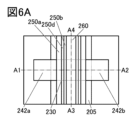
- FIG. 6A is a top view showing an example of a semiconductor device.
- 6B and 6C are cross-sectional views showing an example of a semiconductor device.
- FIG. 7A to 7D are cross-sectional views showing an example of a semiconductor device.
- FIG. 8A is a top view showing an example of a semiconductor device.
- FIGS. 8B and 8C are cross-sectional views showing an example of a semiconductor device.
- 9A to 9F are cross-sectional views showing an example of a semiconductor device.
- 10A to 10F are cross-sectional views showing an example of a semiconductor device.
- 11A to 11D are cross-sectional views showing an example of a semiconductor device.
- 12A to 12D are cross-sectional views showing an example of a semiconductor device.
- 13A to 13F are cross-sectional views showing an example of a semiconductor device.
- 14A to 14F are cross-sectional views showing an example of a semiconductor device.
- 15A is a top view showing an example of a semiconductor device.
- 15B to 15D are cross-sectional views showing an example of a semiconductor device.
- 16A and 16B are cross-sectional views showing an example of a semiconductor device.
- 17A and 17B are cross-sectional views showing an example of a semiconductor device.
- 18A and 18B are cross-sectional views showing an example of a semiconductor device.
- FIG. 19A is a top view showing an example of a semiconductor device.
- 19B and 19C are cross-sectional views showing an example of a semiconductor device.
- FIG. 20A is a top view showing an example of a semiconductor device.
- FIG. 20B is a cross-sectional view showing an example of a semiconductor device.
- FIG. 20A is a top view showing an example of a semiconductor device.
- FIG. 20B is a cross-sectional view showing an example of a semiconductor device.
- FIG. 20A is a top view showing an example of a semiconductor device.
- FIG. 21 is a cross-sectional view showing an example of a semiconductor device.
- FIG. 22 is a cross-sectional view showing an example of a semiconductor device.
- FIG. 23A is a top view showing an example of a semiconductor device.
- FIG. 23B is a cross-sectional view showing an example of a semiconductor device.
- FIG. 24A is a top view showing an example of a semiconductor device.
- FIG. 24B is a cross-sectional view showing an example of a semiconductor device.
- FIG. 25A is a top view showing an example of a semiconductor device.
- FIG. 25B is a cross-sectional view showing an example of a semiconductor device.
- FIG. 26 is a cross-sectional view showing an example of a storage device.
- FIG. 23A is a top view showing an example of a semiconductor device.
- FIG. 23B is a cross-sectional view showing an example of a semiconductor device.
- FIG. 24A is a top view showing an example of a semiconductor
- FIG. 27 is a cross-sectional view showing an example of a storage device.
- FIG. 28A is a block diagram illustrating a configuration example of a storage device according to one embodiment of the present invention.
- FIG. 28B is a perspective view illustrating a configuration example of a storage device according to one embodiment of the present invention.
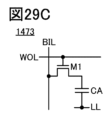
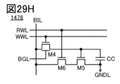
- 29A to 29I are circuit diagrams illustrating a configuration example of a storage device according to one embodiment of the present invention.
- FIG. 30 is a cross-sectional view showing an example of a storage device.
- FIG. 31A is a diagram illustrating an example of a circuit configuration of a memory cell.
- FIG. 31B is a graph showing an example of hysteresis characteristics.
- FIG. 31C is a timing chart showing an example of a method for driving a memory cell.
- FIGS. 32A and 32B are schematic diagrams of a semiconductor device according to one embodiment of the present invention.
- 33A to 33E are diagrams for explaining an example of a storage device.
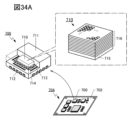
- 34A and 34B are diagrams showing an example of an electronic component.
- 35A and 35B are diagrams showing an example of an electronic device, and
- FIGS. 35C to 35E are diagrams showing an example of a large-sized computer.
- FIG. 36 is a diagram showing an example of space equipment.
- FIG. 37 is a diagram illustrating an example of a storage system applicable to a data center.
- FIG. 38 is a diagram showing the GIXRD measurement results.
- FIGS. 39A and 39B are diagrams showing the results of surface observation using AFM.
- FIGS. 39C and 39D are diagrams showing the results of image analysis.
- FIG. 40A is a diagram showing an input voltage waveform.
- FIG. 40B is a diagram showing P-E characteristics.
- FIG. 41A is a diagram showing an input voltage waveform.
- FIG. 41B is a diagram showing fatigue characteristics.
- FIGS. 42A and 42B are diagrams showing fatigue characteristics.
- FIGS. 43A and 43B are diagrams illustrating a retention measurement method.
- FIG. 44 is a diagram showing the results of retention measurement.
- FIG. 45 is a diagram showing J-V characteristics.
- FIG. 46 is a cross-sectional STEM image of the prepared sample.
- FIG. 47A is a diagram illustrating a memory cell circuit.
- FIG. 47B is an optical micrograph.
- FIGS. 49A and 49B are diagrams illustrating a method of writing and reading evaluation of positive polarization.
- FIGS. 50A and 50B are diagrams illustrating a method of writing and reading evaluation of positive polarization.
- FIG. 51 is a diagram showing voltage waveforms.
- FIG. 52 is a diagram showing changes in ⁇ V BL .
- FIG. 53 is a diagram showing changes in ⁇ V BL .
- FIGS. 54A and 54B are diagrams showing fatigue characteristics.
- FIGS. 55A and 55B are diagrams showing the results of retention measurement.
- FIG. 56A is a schematic diagram of the sample, and FIG. 56B is a cross-sectional view of the sample.
- FIG. 56A is a schematic diagram of the sample
- FIG. 56B is a cross-sectional view of the sample.
- FIG. 57 is a cross-sectional STEM image of the prepared sample.
- FIG. 58 is a diagram showing the Id-Vg characteristics of the sample.
- FIG. 59 is a diagram showing threshold voltages.
- FIG. 60 is a diagram showing the Id-Vg characteristics of the sample.
- FIG. 61A is a diagram showing the threshold voltage of the sample.
- FIG. 61B is a diagram showing the sheet resistance of the sample.
- FIG. 61C is a diagram showing the contact resistance of the sample.
- FIG. 62 is a diagram showing the Id-Vg characteristics of the sample.
- 63A to 63C are diagrams showing the contact resistance of the sample.
- FIG. 64A is a circuit diagram showing the circuit configuration of the sample.
- FIG. 64B is a diagram showing measurement results of leakage current.
- FIG. 64A is a circuit diagram showing the circuit configuration of the sample.
- FIG. 64B is a diagram showing measurement results of leakage current.
- FIG. 65A is a circuit diagram showing the circuit configuration of the sample.
- FIG. 65B is a circuit diagram showing the Id-V CWL characteristics of the sample.
- FIG. 65C is a diagram showing the potential Vsh of the sample.
- FIG. 66A is a diagram showing the results of a sample data retention evaluation test.
- FIG. 66B is a diagram showing the results of a sample data rewriting evaluation test.
- FIG. 67A is a diagram showing contact resistance.
- FIG. 67B is a diagram showing sheet resistance.
- FIG. 68 is a cross-sectional STEM image according to the example.
- FIGS. 69A and 69B are diagrams showing the results of the drain withstand voltage test.
- FIG. 70 is a diagram showing the results of the drain withstand voltage test.
- FIG. 71 is a diagram showing PV characteristics.
- FIG. 72 is a diagram showing fatigue characteristics.
- FIG. 73 is a diagram showing changes in ⁇ V BL .
- ordinal numbers such as “first” and “second” are used for convenience, and do not limit the number of components or the order of the components (for example, the order of steps or the order of lamination). It's not something you do. Further, the ordinal number attached to a constituent element in a certain part of this specification may not match the ordinal number attached to the constituent element in another part of this specification or in the claims.
- film and “layer” can be interchanged depending on the situation or circumstances.
- conductive layer can be changed to the term “conductive film.”
- insulating film can be changed to the term “insulating layer.”
- conductor can be interchanged with the term “conductive layer” or the term “conductive film” depending on the case or the situation.
- insulator can be interchanged with the term “insulating layer” or the term “insulating film” depending on the case or the situation.
- the opening includes, for example, a groove, a slit, etc. Further, a region in which an opening is formed may be referred to as an opening.
- drawings used in this embodiment show a case where the sidewall of the insulator in the opening of the insulator is approximately perpendicular to the substrate surface or the surface to be formed, it may have a tapered shape.
- a tapered shape refers to a shape in which at least a part of the side surface of the structure is inclined with respect to the substrate surface or the surface to be formed.
- a taper angle a region where the angle between the inclined side surface and the substrate surface or the surface to be formed (hereinafter sometimes referred to as a taper angle) is less than 90°.
- the side surfaces of the structure and the substrate surface do not necessarily have to be completely flat, and may be substantially planar with minute curvatures or substantially planar with minute irregularities.
- the heights match refers to a configuration in which the heights from a reference surface (for example, a flat surface such as a substrate surface) are equal in cross-sectional view.
- a reference surface for example, a flat surface such as a substrate surface
- the surface of a single layer or a plurality of layers may be exposed by performing a planarization process (typically a CMP (Chemical Mechanical Polishing) process).
- CMP Chemical Mechanical Polishing
- the surfaces to be subjected to CMP processing have the same height from the reference surface.
- the heights of the plurality of layers may differ depending on the processing apparatus, processing method, or material of the surface to be processed during CMP processing.
- the heights match In this specification, this case is also treated as "the heights match.”
- the height of the top surface of the first layer and the height of the second layer are If the difference from the height of the top surface of the layer is 20 nm or less, it is also said that the heights match.
- the ends coincide means that at least a portion of the outlines of the stacked layers overlap when viewed from above. For example, this includes a case where the upper layer and the lower layer are processed using the same mask pattern or partially the same mask pattern. However, strictly speaking, the contours do not overlap, and the contour of the upper layer may be located inside the contour of the lower layer, or the contour of the upper layer may be located outside the contour of the lower layer. "Concordance”.
- match includes both a complete match and a general match.
- off-state current may refer to, for example, a current flowing between a source and a drain when a transistor is in an off state.
- a configuration example of a semiconductor device that is one embodiment of the present invention will be described with reference to FIGS. 1A to 25B.
- a semiconductor device that is one embodiment of the present invention includes a transistor.
- An insulator 280 is provided on the insulator 222, the conductor 242a, and the conductor 242b.
- the upper surface of insulator 280 may be flattened.
- an insulator 250 and a conductor 260 are provided so as to fill the opening formed in the insulator 280.
- the oxide 230 has a region that functions as a channel formation region.
- the conductor 260 has a region that functions as a first gate electrode (upper gate electrode).
- Insulator 250 has a region that functions as a first gate insulator.
- the conductor 205 has a region that functions as a second gate electrode (lower gate electrode).
- Insulator 222 has a region that functions as a second gate insulator.
- the conductor 242a has a region that functions as either a source electrode or a drain electrode.
- the conductor 242b has a region that functions as the other of a source electrode and a drain electrode.
- the oxide 230 has a region that functions as a channel formation region, in this specification and the like, the oxide 230 can be referred to as a semiconductor layer of the transistor 200A. Further, the semiconductor layer can be referred to as the oxide 230.
- the carrier concentration of the region 230i is 1 ⁇ 10 18 cm ⁇ 3 or less, less than 1 ⁇ 10 17 cm ⁇ 3 , less than 1 ⁇ 10 16 cm ⁇ 3 , less than 1 ⁇ 10 15 cm ⁇ 3 , or 1 ⁇ 10 14 cm -3, less than 1 ⁇ 10 13 cm ⁇ 3 , less than 1 ⁇ 10 12 cm ⁇ 3 , less than 1 ⁇ 10 11 cm ⁇ 3 , or preferably less than 1 ⁇ 10 10 cm ⁇ 3 .
- the lower limit value of the carrier concentration in the region 230i is not particularly limited, but may be set to, for example, 1 ⁇ 10 ⁇ 9 cm ⁇ 3 .
- the oxide 230 may have a single layer structure or a laminated structure.
- the element M includes aluminum, gallium, tin, yttrium, titanium, vanadium, chromium, manganese, iron, cobalt, nickel, zirconium, molybdenum, hafnium, tantalum, tungsten, lanthanum, cerium, neodymium, magnesium, and calcium. , strontium, barium, boron, silicon, germanium, and antimony.
- the element M included in the metal oxide is preferably one or more of the above elements, more preferably one or more selected from aluminum, gallium, tin, and yttrium, and further gallium. preferable. Note that in this specification and the like, metal elements and metalloid elements may be collectively referred to as "metal elements," and the "metal elements" described in this specification and the like may include semimetal elements.
- the field effect mobility of the transistor can be increased.
- the metal oxide may contain one or more metal elements having a large periodic number in the periodic table of elements.
- Metal elements with large period numbers in the periodic table of elements include metal elements belonging to the fifth period, metal elements belonging to the sixth period, and the like.
- the metal oxide becomes highly crystalline, and the diffusion of impurities in the metal oxide can be suppressed. . Therefore, fluctuations in the electrical characteristics of the transistor are suppressed, and reliability can be improved.
- the transistor can obtain a large on-current and high frequency characteristics.
- metal oxides can be used.
- the nearby composition includes a range of ⁇ 30% of the desired atomic ratio.
- the element M it is preferable to use at least one of gallium and aluminum.
- the above atomic ratio is not limited to the atomic ratio of the formed metal oxide, but also the atomic ratio of the sputtering target used for forming the metal oxide film. It may be.
- the channel formation region in the oxide semiconductor preferably has a reduced carrier concentration and is i-type (intrinsic) or substantially i-type.
- the insulator can be converted to an oxide semiconductor. It can supply oxygen and reduce oxygen vacancies and V OH .
- excess oxygen oxygen that is desorbed by heating
- the insulator can be converted to an oxide semiconductor. It can supply oxygen and reduce oxygen vacancies and V OH .
- an excessive amount of oxygen is supplied to the region 230na or the region 230nb, there is a risk that the on-state current of the transistor 200A or the field effect mobility will decrease.
- the amount of oxygen supplied to the region 230na or the region 230nb varies within the substrate plane, resulting in variations in the characteristics of a semiconductor device including a transistor.
- the region 230i has a reduced carrier concentration and is preferably i-type or substantially i-type, whereas the region 230na and the region 230nb have a high carrier concentration and are n-type. is preferred.
- an excessive amount of oxygen is not supplied to the region 230na and the region 230nb, and that the amount of V OH in the region 230na and the region 230nb is not excessively reduced.
- the oxide semiconductor can form V OH , so in order to reduce the amount of V OH , it is necessary to reduce the hydrogen concentration.
- the semiconductor device is configured to supply oxygen to the region 230i and suppress the diffusion of hydrogen to the region 230i. Further, the semiconductor device has a structure in which oxidation of the conductor 242a, the conductor 242b, and the conductor 260 is suppressed. Further, the semiconductor device is configured to reduce the hydrogen concentration in the region 230i.
- the conductor 260 covers the side and top surfaces of the oxide 230.
- the channel formation region can be electrically surrounded by the electric field of the gate electrode.
- a structure of a transistor in which a channel formation region is electrically surrounded by at least the electric field of the first gate electrode is referred to as a surrounded channel (S-channel) structure.
- a laminate of the first insulator on the channel forming region and the second insulator on the first insulator is referred to as a first laminate.
- a laminate of the first insulator under the region 230i and the second insulator under the first insulator is referred to as a second laminate.
- the first stacked body and the second stacked body are provided symmetrically with respect to the channel forming region as a reference or axis.
- the first stacked body and the second stacked body are provided symmetrically with respect to a plane or a line passing through the channel forming region.
- the first stacked body and the second stacked body are provided symmetrically with respect to the channel forming region.
- a configuration in which the first laminate and the second laminate are provided symmetrically with respect to the structure means that the first laminate and the second laminate are arranged symmetrically with respect to the structure.
- the first laminate and the second laminate are provided to sandwich the structure, and in the direction from the first laminate to the second laminate via the structure, Refers to a configuration in which the stacking order of the layers included in the first laminate is opposite to the stacking order of the layers included in the second laminate.
- first laminate, the structure, and the second laminate may be arranged in this order in a direction perpendicular to the substrate surface, or may be arranged in a horizontal direction with respect to the substrate surface.
- first laminate, the structure, and the second laminate are arranged in this order in a direction perpendicular to the substrate surface, the first laminate and the second laminate are It can be said that they are provided above and below the .
- first laminate and the second laminate each have two or more layers. Further, it is preferable that the number of layers included in the first laminate is the same as the number of layers included in the second laminate. Note that one layer included in the first laminate may have the functions of multiple layers included in the second laminate, and vice versa. Further, a structure comprised of a plurality of layers included in the first laminate may have the function of one layer included in the second laminate, and vice versa. Therefore, the number of layers included in the first laminate and the number of layers included in the second laminate may be different. Moreover, the contours of one layer and another layer included in the first laminate do not necessarily have to overlap. The same applies to the second laminate.
- the semiconductor device shown in this embodiment includes a first stacked body, a metal oxide having a channel formation region under the first stacked body, and a second stacked body under the metal oxide.
- the first laminate and the second laminate each include at least a first insulator and a second insulator.
- the first insulator of the first laminate and the first insulator of the second laminate have a region that overlaps with each other via the channel forming region
- the second insulator included in the second stacked body and the second insulator included in the second stacked body are the first insulator included in the first stacked body, the channel forming region, and the first insulator included in the second stacked body. They have regions that overlap each other with an insulator in between.
- the insulator 250 preferably has a laminated structure of an insulator 250a and an insulator 250b on the insulator 250a.
- the insulator 222 preferably has a laminated structure of an insulator 222a and an insulator 222b below the insulator 222a.
- the insulator 250a and the insulator 222a may be provided to sandwich the region 230i of the oxide 230
- the insulator 250b and the insulator 222b may be provided to sandwich the insulator 250a, the region 230i, and the insulator 222a. preferable.
- the insulator 250a and the insulator 222a have a region that overlaps with each other via the region 230i
- the insulator 250b and the insulator 222b have a region that overlaps with each other via the region 230i and the insulator 222a. have areas that overlap with each other.
- an insulator that easily transmits oxygen As the insulator 250a and the insulator 222a, oxygen contained in the insulator 280 can be supplied to the region 230i via the insulator 250a and the insulator 222a. Further, as the insulator 250a and the insulator 222a, an insulator containing excess oxygen may be used. With such a configuration, oxygen contained in the insulator 250a and the insulator 222a can be supplied to the region 230i.
- the concentration of impurities such as water and hydrogen in the insulator 250a and the insulator 222a is reduced.
- the ratio of the permittivity of a medium to the permittivity of a vacuum is called the relative permittivity.
- the relative dielectric constant is the dielectric constant made dimensionless by an electric constant. Therefore, the dielectric constant can be referred to as the relative dielectric constant.
- the concentration of impurities such as water and hydrogen in the insulator 280 is reduced.
- the insulator 280 preferably includes an oxide containing silicon, such as silicon oxide or silicon oxynitride.
- the conductor 260 and the insulator 250 are arranged to fill the opening formed in the insulator 280.
- the conductor 260 is provided in the opening so as to cover at least a portion of the side surface and at least a portion of the top surface of the oxide 230 with the insulator 250 interposed therebetween. Further, the conductor 260 is arranged so that its upper surface is at the same height as the upper surface of the insulator 250 and the upper surface of the insulator 280.
- the side wall of the insulator 280 may be approximately perpendicular to the upper surface of the insulator 222, and may have a tapered shape. It may be. By tapering the sidewall of the insulator 280 in the opening, the coverage of the insulator 250 provided in the opening can be improved and defects such as holes can be reduced.
- the conductor 260 preferably extends in the channel width direction, as shown in FIGS. 1A and 1C. With this structure, the conductor 260 functions as a wiring when a plurality of transistors are provided.
- the conductor 260, the conductor 242a, the conductor 242b, and the conductor 205 it is preferable to use a conductive material that is not easily oxidized or a conductive material that has a function of suppressing oxygen diffusion, respectively.
- the conductive material include a conductive material containing nitrogen and a conductive material containing oxygen.
- the conductor 260, the conductor 242a, the conductor 242b, and the conductor 205 are at least Contains metal and nitrogen.
- the conductor 260 may have a single layer structure or a laminated structure. Further, the conductor 242a and the conductor 242b may have a single layer structure or a laminated structure.
- a conductive material containing nitrogen for example, a nitride containing tantalum, a nitride containing titanium, a nitride containing molybdenum, a nitride containing tungsten, tantalum, and the like. It is preferable to use a nitride containing aluminum, a nitride containing titanium and aluminum, or the like. In one aspect of the invention, nitrides containing tantalum are particularly preferred.
- ruthenium, ruthenium oxide, ruthenium nitride, an oxide containing strontium and ruthenium, an oxide containing lanthanum and nickel, etc. may be used. These materials are preferable because they are conductive materials that are not easily oxidized or materials that maintain conductivity even after absorbing oxygen.
- the conductor 205 is arranged so as to overlap the oxide 230 and the conductor 260. Furthermore, the conductor 205 is preferably provided extending in the channel width direction, as shown in FIGS. 1A and 1C. With this structure, the conductor 205 functions as a wiring when a plurality of transistors are provided.
- the conductor 205 may have a single layer structure or a laminated structure.
- the conductor 205 can function as a second gate electrode.
- the threshold voltage (Vth) of the transistor 200 can be controlled by changing the potential applied to the conductor 205 independently of the potential applied to the conductor 260 without interlocking with the potential applied to the conductor 260.
- the Vth of the transistor 200 can be increased and the off-state current can be decreased. Therefore, when a negative potential is applied to the conductor 205, the drain current when the potential applied to the conductor 260 is 0 V can be made smaller than when no negative potential is applied.
- the potential applied to the conductor 205 may be the same as the potential applied to the conductor 260.
- the electric fields of the conductor 260 and the conductor 205 can be applied to the entire channel formation region of the oxide 230. Therefore, the channel width can be increased without increasing the size of the transistor. Therefore, the on-state current of the transistor can be increased while miniaturizing the transistor. Furthermore, by increasing the on-state current of the transistor, frequency characteristics can be improved.
- FIGS. 1B and 1C show a structure in which a stacked structure of an insulator 222b and an insulator 222a is used as the second gate insulator
- the present invention is not limited to this.
- a stack of the insulator 222 and an island-shaped insulator on the insulator 222 may be used as the second gate insulator.
- an island-shaped insulator may be provided between the insulator 222 and the oxide 230.
- island-like refers to a state in which two or more layers formed in the same process and using the same material are physically separated.
- FIGS. 2A and 2B are cross-sectional views of a semiconductor device including a transistor 200A.
- FIG. 2A is a cross-sectional view of the transistor 200A in the channel length direction
- FIG. 2B is a cross-sectional view of the transistor 200A in the channel width direction.
- FIG. 1A can be referred to for a top view of the semiconductor device shown in FIGS. 2A and 2B.
- the transistor 200A shown in FIGS. 2A and 2B differs from the transistor 200A shown in FIGS. 1B and 1C mainly in that the insulator 222 is a single layer and that the transistor 200A has an island-like insulator 224.
- an island-shaped insulator 224 is provided between the insulator 222 and the oxide 230.
- the side edges of the insulator 224 coincide with the side edges of the oxide 230.
- Each of the insulators 222 and 224 has a region that functions as a second gate insulator.
- the insulator 250a has a region in contact with the top surface of the insulator 222, a region in contact with the side surface of the insulator 224, a region in contact with the side surface of the oxide 230, and a region in contact with the top surface of the oxide 230. At this time, the region 230i of the oxide 230 is surrounded by the insulator 250a and the insulator 224.
- the insulator 222 it is preferable to use a material that can be applied to the above-mentioned insulator 222b. Moreover, it is preferable that the insulator 224 uses a material that can be applied to the above-mentioned insulator 222a. In such a configuration, the laminate consisting of the insulator 222 and the island-shaped insulator 224 can be regarded as a second laminate. At this time, it can be said that the transistor 200A shown in FIGS. 2A and 2B has a configuration in which the first stacked body and the second stacked body are provided symmetrically with respect to the channel formation region.
- FIG. 3A is a top view of the semiconductor device
- FIGS. 3B and 3C are cross-sectional views of the semiconductor device.
- FIG. 3B is a sectional view of a portion indicated by a dashed line A1-A2 in FIG. 3A.
- FIG. 3C is a cross-sectional view of a portion shown by a dashed line A3-A4 in FIG. 3A. Note that in the top view of FIG. 3A, some elements are omitted for clarity.
- FIGS. 3A to 3C includes a transistor 200B. Therefore, FIG. 3B can also be said to be a cross-sectional view of the transistor 200B in the channel length direction. Further, FIG. 3C can also be said to be a cross-sectional view of the transistor 200B in the channel width direction.
- the transistor 200B shown in FIGS. 3B and 3C mainly differs from the transistor 200A shown in FIGS. 1B and 1C in that each of the insulator 222 and the insulator 250 has a three-layer stacked structure.
- the insulator 250 further includes an insulator 250c below the insulator 250a
- the insulator 222 further includes an insulator 222c above the insulator 222a. This is the main difference from the transistor 200A shown in FIGS. 1B and 1C.
- portions that are different from the above-described configuration example 1 will be mainly explained, and descriptions of overlapping portions will be omitted.
- the insulator 250 includes an insulator 250c, an insulator 250a on the insulator 250c, and an insulator 250b on the insulator 250a.
- the insulator 222 includes an insulator 222b, an insulator 222a on the insulator 222b, and an insulator 222c on the insulator 222a.
- the insulator 250c and the insulator 222c have a region that overlaps with each other via the region 230i
- the insulator 250a and the insulator 222a have a region that overlaps with each other via the insulator 250c, the region 230i, and the insulator 222c.
- the insulator 250c and the insulator 222c have barrier properties against oxygen.
- the insulator 250c has a region in contact with the side surface of the conductor 242a and a region in contact with the side surface of the conductor 242b. Since the insulator 250c has barrier properties against oxygen, the side surfaces of the conductor 242a and the conductor 242b can be prevented from being oxidized and formation of an oxide film on the side surfaces. This can suppress the on-state current of the transistor 200B from becoming small or the field-effect mobility from decreasing.
- barrier insulators against oxygen include oxides containing one or both of aluminum and hafnium, oxides containing hafnium and silicon (hafnium silicate), magnesium oxide, gallium oxide, gallium zinc oxide, and indium gallium zinc oxide. , silicon nitride, and silicon nitride oxide.
- oxides containing one or both of aluminum and hafnium include aluminum oxide, hafnium oxide, and oxides containing aluminum and hafnium (hafnium aluminate).
- the insulator 222c is provided between the insulator 222a and the region 230na or the region 230nb. Therefore, diffusion of oxygen from below the insulator 222c to the regions 230na and 230nb can be suppressed. Further, a conductor 242a is provided on the region 230na, and a conductor 242b is provided on the region 230nb. Therefore, in this embodiment, an excessive amount of oxygen is not supplied to the region 230na and the region 230nb.
- insulator 250c and the insulator 222c it is preferable to use an insulator containing an oxide containing one or both of aluminum and hafnium as the insulator 250c and the insulator 222c.
- aluminum oxide is used as the insulator 250c and the insulator 222c.
- each of the insulator 250c and the insulator 222c contains at least oxygen and aluminum.
- the insulator 250c and the insulator 222c have the same function. Therefore, the first stacked body and the second stacked body can be provided symmetrically with respect to the channel formation region.
- the insulator 250c has a region in contact with the top surface of the insulator 222a, a region in contact with the side surface of the insulator 224, a region in contact with the side surface of the oxide 230, and a region in contact with the top surface of the oxide 230. At this time, the region 230i of the oxide 230 is surrounded by the insulator 250c and the insulator 224.
- FIGS. 4A and 4B show a configuration in which an insulator 224 having barrier properties against oxygen is provided between the region 230i and the insulator 222a, the present invention is not limited to this.
- An example of a configuration different from the configuration shown in FIGS. 4A and 4B is shown in FIGS. 5A and 5B.
- the transistor 200B shown in FIGS. 5A and 5B has the following points: the insulator 222 has a two-layer stacked structure, the insulator 224 is not included, and the oxide 230 has a two-layer stacked structure.
- the transistor 200B is mainly different from the transistor 200B shown in FIG.
- the insulator 222 has a stacked structure of an insulator 222b and an insulator 222a on the insulator 222b.
- the oxide 230 has a stacked structure of an oxide 230a and an oxide 230b on the oxide 230a. It is preferable that the oxide 230a be made of a semiconductor material having barrier properties against oxygen, and the oxide 230b be made of a material that can be used for the oxide 230 described above.
- the oxide 230a only needs to be less permeable to oxygen than, for example, the insulator 222a. Further, as the oxide 230a, for example, a material that is less permeable to oxygen than the insulator 222a may be used.
- the laminate made of the insulator 222 and the oxide 230a can be regarded as the second laminate.
- the transistor 200B shown in FIGS. 5A and 5B has a configuration in which the first stacked body and the second stacked body are provided symmetrically with respect to the channel formation region.
- the region 230i, the region 230na, and the region 230nb may be formed not only in the oxide 230b but also in the oxide 230a. be.
- the insulator 222 may have a single layer structure, and an insulator 224 may be provided between the insulator 222 and the oxide 230a.
- the insulator 250c and the oxide 230a have a region that overlaps with each other via the region 230i
- the insulator 250a and the insulator 224 have a region that overlaps with each other via the insulator 250c, the region 230i, and the oxide 230a.
- the insulator 250b and the insulator 222 have an overlapping region with the insulator 250a, the insulator 250c, the region 230i, the oxide 230a, and the insulator 224 interposed therebetween.
- FIGS. 6A to 6C includes a transistor 200C. Therefore, FIG. 6B can also be said to be a cross-sectional view of the transistor 200C in the channel length direction. Further, FIG. 6C can also be said to be a cross-sectional view of the transistor 200C in the channel width direction.
- the transistor 200C shown in FIGS. 6B and 6C mainly differs from the transistor 200A shown in FIGS. 1B and 1C in that each of the insulator 222 and the insulator 250 has a three-layer stacked structure.
- the transistor 200C shown in FIGS. 6B and 6C includes an insulator 250d between an insulator 250a and an insulator 250b, and an insulator 222d between an insulator 222a and an insulator 222b. This is the main difference from the transistor 200A shown in FIGS. 1B and 1C.
- portions that are different from the above-described configuration example 1 will be mainly explained, and descriptions of overlapping portions will be omitted.
- the insulator 250d and the insulator 222d have a function of capturing or fixing hydrogen.
- hydrogen inside the region can be captured or fixed more effectively. be able to.
- hydrogen contained in the insulator 250a, the region 230i of the oxide 230b, and the insulator 222a can be captured or fixed more effectively. Therefore, the hydrogen concentration in the region 230i can be reduced. Therefore, the V O H in region 230i can be reduced, making region 230i i-type or substantially i-type.
- Examples of insulators that have the function of capturing or fixing hydrogen include metal oxides with an amorphous structure.
- metal oxides with an amorphous structure As the insulator 250d and the insulator 222d, it is preferable to use, for example, a metal oxide such as magnesium oxide or an oxide containing one or both of aluminum and hafnium.
- metal oxides having such an amorphous structure oxygen atoms have dangling bonds, and the dangling bonds may capture or fix hydrogen.
- metal oxides having an amorphous structure have a high ability to capture or fix hydrogen.
- a material with a high dielectric constant (high-k) for the insulator 250d and the insulator 222d.
- high-k materials include oxides containing one or both of aluminum and hafnium, tantalum oxide, zirconium oxide, hafnium zirconium oxide, and the like.
- problems such as leakage current may occur due to thinning of gate insulators.
- a high-k material as the insulator 250d and the insulator 222d, it is possible to reduce the gate potential applied during transistor operation while maintaining the physical thickness of the gate insulator.
- EOT equivalent oxide thickness
- a substance with a high dielectric constant such as lead zirconate titanate (PZT), strontium titanate (SrTiO 3 ), (Ba,Sr)TiO 3 (BST) can be used. In some cases.
- hafnium oxide is used as the insulator 250d and the insulator 222d.
- each of the insulator 250d and the insulator 222d contains at least oxygen and hafnium.
- the hafnium oxide has an amorphous structure.
- the insulator 250d and the insulator 222d have an amorphous structure.
- the insulator 250d and the insulator 222d have the same function. Therefore, the first stacked body and the second stacked body can be provided symmetrically with respect to the channel formation region.
- the second gate insulator may be composed of a stacked body of an insulator 222 and an island-shaped insulator 224.
- FIGS. 7A and 7B are cross-sectional views of a semiconductor device including a transistor 200C.
- FIG. 7A is a cross-sectional view of the transistor 200C in the channel length direction
- FIG. 7B is a cross-sectional view of the transistor 200C in the channel width direction. Note that FIG. 6A can be referred to for a top view of the semiconductor device shown in FIGS. 7A and 7B.
- the insulator 250a has a region in contact with the top surface of the insulator 222d, a region in contact with the side surface of the insulator 224, a region in contact with the side surface of the oxide 230, and a region in contact with the top surface of the oxide 230. At this time, the region 230i of the oxide 230 is surrounded by the insulator 250a and the insulator 224.
- the insulator 224 is preferably made of a material that can be used for the insulator 222a described above.
- FIGS. 7C and 7D are cross-sectional views of a semiconductor device including a transistor 200C.
- FIG. 7C is a cross-sectional view of the transistor 200C in the channel length direction
- FIG. 7D is a cross-sectional view of the transistor 200C in the channel width direction.
- FIG. 6A can be referred to for a top view of the semiconductor device shown in FIGS. 7C and 7D.
- FIGS. 8A to 8C Configuration examples different from the above-described transistors 200A to 200C are shown in FIGS. 8A to 8C.
- FIG. 8A is a top view of the semiconductor device
- FIGS. 8B and 8C are cross-sectional views of the semiconductor device.
- FIG. 8B is a sectional view of a portion shown by a dashed line A1-A2 in FIG. 8A.
- FIG. 8C is a cross-sectional view of the portion shown by the dashed line A3-A4 in FIG. 8A. Note that in the top view of FIG. 8A, some elements are omitted for clarity.
- the body 222b includes an insulator 250d, an insulator 250a, an insulator 250c, a region 230i, an insulator 222c, an insulator 222a, and a region that overlaps each other via an insulator 222d.
- the transistor 200D shown in FIGS. 9A and 9B, the transistor 200D shown in FIGS. 9C and 9D, and the transistor 200D shown in FIGS. 9E and 9F have an island-shaped insulator 224 between the insulator 222 and the oxide 230. This is the main difference from the transistor 200D shown in FIGS. 8B and 8C.
- the insulator 222 has a single-layer structure, and the insulator 224 includes an insulator 224d, an insulator 224a on the insulator 224d, and an insulator 224a on the insulator 224a. It has a laminated structure with 224c.
- the insulator 222 it is preferable to use a material that can be used for the above-mentioned insulator 222b.
- the insulator 224d is made of a material applicable to the above-mentioned insulator 222d
- the insulator 224a is made of a material applicable to the above-described insulator 222a
- the insulator 224c is made of a material applicable to the above-described insulator 222c. It is preferable to use
- the laminate consisting of the insulator 222 and the insulator 224 can be regarded as a second laminate.
- the first stacked body and the second stacked body have a channel It can be said that the configuration is symmetrical with respect to the formation area.
- the transistor 200D shown in FIGS. 10A and 10B differs from the transistor 200D shown in FIGS. 8B and 8C mainly in that the oxide 230 has a two-layer stacked structure.
- the transistor 200D shown in FIGS. 10C and 10D and the transistor 200D shown in FIGS. 10E and 10F have the island-shaped insulator 224 and the oxide 230 has a two-layer stacked structure. This is mainly different from the transistor 200D shown in 8C.
- the insulator 224 includes an insulator 224d and an insulator 224a on the insulator 224d.
- the oxide 230 has a stacked structure of an oxide 230a and an oxide 230b on the oxide 230a.
- the insulator 222 it is preferable to use a material that can be used for the above-mentioned insulator 222b.
- the insulator 224d uses a material that can be used for the above-described insulator 222d
- the insulator 224a uses a material that can be used for the above-described insulator 222a.
- the laminate consisting of the insulator 222, the insulator 224, and the oxide 230a can be regarded as a second laminate.
- the first stacked body and the second stacked body are provided symmetrically with respect to the channel formation region. It can be said that it has a structure.
- FIGS. 11A and 11B, FIG. 11C and FIG. 11D, FIG. 12A and FIG. 12B, and FIG. 12C and FIG. 12D are respectively cross-sectional views of a semiconductor device having a transistor 200D.
- FIGS. 11A, 11C, 12A, and 12C are cross-sectional views of the transistor 200D in the channel length direction
- FIGS. 11B, 11D, 12B, and 12D are cross-sectional views of the transistor 200D in the channel width direction. It is.
- the top view of the semiconductor device shown in FIGS. 11A and 11B and the semiconductor device shown in FIGS. 11C and 11D can be seen in FIG. 3A, and the top view of the semiconductor device shown in FIGS.
- FIG. 8A For a top view of the illustrated semiconductor device, see FIG. 8A.
- the transistor 200D shown in FIGS. 11A and 11B and the transistor 200D shown in FIGS. 11C and 11D have an insulator 222d and do not have an insulator 250d.
- the transistor 200D shown in FIGS. 11A and 11B differs from the transistor 200B shown in FIGS. 4C and 4D in that it includes an insulator 222d. Further, the transistor 200D shown in FIGS. 11A and 11B differs from the transistor 200D shown in FIGS. 9C and 9D in that it does not include an insulator 250d. Therefore, the transistor 200D shown in FIGS. 11A and 11B can be said to be a modification of the transistor 200B shown in FIGS. 4C and 4D, or a modification of the transistor 200D shown in FIGS. 9C and 9D.
- the transistor 200D shown in FIGS. 11C and 11D differs from the transistor 200B shown in FIGS. 5C and 5D in that an insulator 222d is provided between the insulator 222b and the insulator 224. Further, the transistor 200D shown in FIGS. 11C and 11C differs from the transistor 200D shown in FIGS. 10C and 10D in that it does not include an insulator 250d. Therefore, the transistor 200D shown in FIGS. 11C and 11D can be said to be a modification of the transistor 200B shown in FIGS. 5C and 5D, or a modification of the transistor 200D shown in FIGS. 10C and 10D. Further, the transistor 200D shown in FIGS. 10C and 10D has a structure in which an insulator 250d is provided between an insulator 250a and an insulator 250b in the transistor 200D shown in FIGS. 11C and 11D.
- the transistor 200D shown in FIGS. 12A and 12B and the transistor 200D shown in FIGS. 12C and 12D have an insulator 250d and do not have an insulator 222d.
- the transistor 200D shown in FIGS. 12A and 12B differs from the transistor 200B shown in FIGS. 4C and 4D in that it includes an insulator 250d. Furthermore, the transistor 200D shown in FIGS. 12A and 12B differs from the transistor 200D shown in FIGS. 9C and 9D in that it does not include an insulator 222d. Therefore, the transistor 200D shown in FIGS. 12A and 12B can be said to be a modification of the transistor 200B shown in FIGS. 4C and 4D, or a modification of the transistor 200D shown in FIGS. 9C and 9D.
- the transistor 200D shown in FIGS. 12C and 12D differs from the transistor 200B shown in FIGS. 5C and 5D in that it includes an insulator 250d.
- the transistor 200D shown in FIGS. 12C and 12D has a structure in which an insulator 250d is added to the transistor 200B shown in FIGS. 5C and 5D.
- the transistor 200D shown in FIGS. 12C and 12D differs from the transistor 200D shown in FIGS. 10C and 10D in that it does not include an insulator 222d. Therefore, the transistor 200D shown in FIGS. 12C and 12D can be said to be a modification of the transistor 200B shown in FIGS. 5C and 5D, or a modification of the transistor 200D shown in FIGS. 10C and 10D.
- the insulator 222 of the transistor 200D shown in FIGS. 12A and 12B and the transistor 200D shown in FIGS. 12C and 12D may be made of a material applicable to the insulator 222b described above, or may be made of a material applicable to the insulator 222d described above. Any applicable material may be used.
- the insulator 222 When using a material applicable to the insulator 222d described above as the insulator 222 of the transistor 200D shown in FIGS. 12A and 12B and the transistor 200D shown in FIGS. It is preferable to have a function of suppressing the diffusion of at least one of atoms and hydrogen molecules.
- the insulator 222 preferably has a function of suppressing hydrogen diffusion more than the insulator 224 (the insulator 224a in the transistor 200D shown in FIGS. 12A and 12B).
- the insulator 222 may have a function of suppressing the diffusion of oxygen (for example, at least one of oxygen atoms and oxygen molecules).
- the insulator 222 preferably has a function of suppressing oxygen diffusion more than the insulator 224 (the insulator 224a in the transistor 200D shown in FIGS. 12A and 12B).
- the insulator 222 may be formed using an oxide of one or both of aluminum and hafnium, or an oxide containing hafnium and zirconium. preferable.
- the insulator 222 suppresses the diffusion of impurities such as hydrogen from the substrate side to the oxide 230, and suppresses the release of oxygen from the oxide 230 to the substrate side. Acts as a layer. Therefore, impurities such as hydrogen can be suppressed from diffusing inside the transistor 200D, and generation of oxygen vacancies in the oxide 230 can be suppressed. Further, it is possible to suppress the conductor 205 from reacting with oxygen included in the oxide 230.
- aluminum oxide, bismuth oxide, germanium oxide, niobium oxide, silicon oxide, titanium oxide, tungsten oxide, yttrium oxide, or zirconium oxide may be added to the above insulator.
- these insulators may be nitrided.
- the thickness of the insulator 222 is preferably larger than the thickness of the insulator 250d, and more preferably larger than the sum of the thicknesses of the insulator 250d and the insulator 250b.
- the insulator 222 has a function of capturing or fixing hydrogen, and a function of suppressing diffusion of hydrogen (for example, at least one of hydrogen atoms and hydrogen molecules). It may have.
- the insulator 222 can have both the function of the material applicable to the above-mentioned insulator 222b and the function of the material applicable to the above-described insulator 222d.
- the first stacked body and the second stacked body are aligned with respect to the channel formation region. It can be said that it has a symmetrical configuration.
- an insulator having barrier properties against hydrogen may be provided above the first gate electrode and/or below the second gate electrode.
- FIG. 13A and 13B, FIG. 13C and FIG. 13D, and FIG. 13E and FIG. 13F are respectively cross-sectional views of a semiconductor device having a transistor 200E.
- FIGS. 13A, 13C, and 13E are cross-sectional views of the transistor 200E in the channel length direction
- FIGS. 13B, 13D, and 13F are cross-sectional views of the transistor 200E in the channel width direction.
- FIG. 1A can be referred to for top views of the semiconductor devices shown in FIGS. 13A and 13B, the semiconductor devices shown in FIGS. 13C and 13D, and the semiconductor devices shown in FIGS. 13E and 13F.
- parts that are different from the above-mentioned configuration examples 1 to 4 will be mainly explained, and descriptions of overlapping parts will be omitted.
- an insulator 283 is provided above the conductor 260. Further, in the transistor 200E shown in FIGS. 13C and 13D, an insulator 215 is provided below the conductor 205. Further, in the transistor 200E shown in FIGS. 13E and 13F, an insulator 283 is provided above the conductor 260, and an insulator 215 is provided below the conductor 205.
- the insulator 283 preferably has barrier properties against hydrogen.
- the insulator 283 it is possible to suppress impurities such as hydrogen contained in the structure provided above the insulator 283 from diffusing into the region 230i.
- the insulator 215 has hydrogen barrier properties like the insulator 222b.
- the insulator 215 it is possible to suppress impurities such as hydrogen contained in the structure provided below the insulator 215 from diffusing into the region 230i.
- the insulator 216 is provided over the insulator 215, and the conductor 205 is arranged so as to fill the opening formed in the insulator 216. Furthermore, the top surface of the conductor 205 and the top surface of the insulator 216 match in height.
- the electrical resistivity of the conductor 205 is designed in consideration of the potential applied to the conductor 205, and the film thickness of the conductor 205 is set according to the electrical resistivity. Furthermore, the thickness of the insulator 216 is approximately the same as that of the conductor 205. Here, it is preferable that the film thicknesses of the conductor 205 and the insulator 216 be made as thin as the design of the conductor 205 allows. By reducing the thickness of the insulator 216, the absolute amount of impurities such as hydrogen contained in the insulator 216 can be reduced, so that diffusion of the impurities into the oxide 230 can be suppressed.
- the insulator 216 has a lower dielectric constant than the insulator 215.
- an insulator that can be used as the insulator 280 may be used as the insulator 216.
- the diffusion of hydrogen from above the transistor 200 to the region 230i can be sufficiently suppressed by providing the insulator 283 having the same function as the insulator 250b, a structure in which the insulator 250b is not provided may be used. Further, if the diffusion of hydrogen from below the transistor 200 to the region 230i can be sufficiently suppressed by providing the insulator 215 having the same function as the insulator 222b, a structure in which the insulator 222b is not provided may be used.
- FIG. 14A and 14B, FIG. 14C and FIG. 14D, and FIG. 14E and FIG. 14F are cross-sectional views of a semiconductor device having a transistor 200E.
- FIGS. 14A, 14C, and 14E are cross-sectional views of the transistor 200E in the channel length direction
- FIGS. 14B, 14D, and 14F are cross-sectional views of the transistor 200E in the channel width direction.
- FIG. 8A can be referred to for top views of the semiconductor devices shown in FIGS. 14A and 14B and the semiconductor devices shown in FIGS. 14C and 14D.
- FIG. 3A For a top view of the semiconductor device shown in FIGS. 14E and 14F, refer to FIG. 3A.
- the transistor 200E shown in FIGS. 14A and 14B differs from the transistor 200D shown in FIGS. 9C and 9D in that an insulator 215 is provided and an insulator 222b is not provided. Unlike the transistor 200D shown in FIG. 10D, the transistor 200E shown in FIGS. 14E and 14F is different from the transistor 200E shown in FIGS. 11C and 11D.
- an insulator having the function of capturing or fixing hydrogen can be provided between the conductor 205 and the insulator 216 and the oxide 230. , an increase in hydrogen concentration in the region 230i can be suppressed.
- FIG. 15A is a top view of a semiconductor device having a transistor 200
- FIGS. 15B to 15D are cross-sectional views of the semiconductor device.
- FIG. 15B is a cross-sectional view of a portion indicated by a dashed line A1-A2 in FIG. 15A, and is also a cross-sectional view of the transistor 200 in the channel length direction.
- FIG. 15C is a cross-sectional view of a portion indicated by a dashed line A3-A4 in FIG. 15A, and is also a cross-sectional view of the transistor 200 in the channel width direction.
- FIG. 15D is a cross-sectional view of a portion indicated by a dashed line A5-A6 in FIG.
- FIG. 15A is also a cross-sectional view of the transistor 200 in the channel width direction. Note that in the top view of FIG. 15A, some elements are omitted for clarity. Further, hereinafter, parts that are different from those described above will be mainly explained, and descriptions of overlapping parts will be omitted.
- the transistor 200 includes an insulator 216 over an insulator 215, a conductor 205 (a conductor 205a and a conductor 205b) embedded in the insulator 216, and an insulator over the insulator 216 and the conductor 205.
- An insulator 275 is provided on the insulator 271a and the insulator 271b, and an insulator 280 is provided on the insulator 275.
- the insulator 250 and the conductor 260 are embedded in the openings formed in the insulator 280 and the insulator 275.
- an insulator 282 is provided over the insulator 280, the conductor 260, and the insulator 250.
- an insulator 283 is provided on the insulator 282.
- the insulator 224, the oxide 230, the conductor 242a, and the conductor 242b have shapes in which the side end portions of the insulator 224, the oxide 230, the conductor 242a, and the conductor 242b match each other as described above.
- any one of the transistors 200A to 200E described above may be applied to the transistor 200 shown in FIGS. 15A to 15D.
- FIGS. 17A and 17B show an example in which the configuration of the transistor 200E shown in FIGS. 14C and 14D is applied to the transistor 200 shown in FIGS. 15A to 15D.
- 17A is an enlarged cross-sectional view of the transistor 200 in the channel length direction
- FIG. 17B is an enlarged cross-sectional view of the transistor 200 in the channel width direction.
- the oxide 230 preferably includes an oxide 230a on the insulator 224 and an oxide 230b on the oxide 230a.
- oxide semiconductor having crystallinity it is preferable to use an oxide semiconductor having crystallinity as the oxide 230b.
- oxide semiconductors having crystallinity include CAAC-OS (c-axis aligned crystalline oxide semiconductor), nc-OS (nanocrystalline oxide semiconductor), and polycrystalline oxide semiconductors. Examples include semiconductors, single crystal oxide semiconductors, and the like.
- CAAC-OS c-axis aligned crystalline oxide semiconductor
- nc-OS nanocrystalline oxide semiconductor
- polycrystalline oxide semiconductors examples include semiconductors, single crystal oxide semiconductors, and the like.
- CAAC-OS c-axis aligned crystalline oxide semiconductor
- nc-OS nanocrystalline oxide semiconductor
- polycrystalline oxide semiconductors examples include semiconductors, single crystal oxide semiconductors, and the like.
- CAAC-OS c-axis aligned crystalline oxide semiconductor
- nc-OS nanocrystalline oxide semiconductor
- polycrystalline oxide semiconductors examples include semiconductors, single crystal oxide semiconductors, and the like.
- CAAC-OS c-axi
- CAAC-OS is a metal oxide that has a highly crystalline and dense structure and has few impurities and defects (for example, oxygen vacancies).
- heat treatment at a temperature that does not polycrystallize the metal oxide (e.g., 400°C or higher and 600°C or lower) allows CAAC-OS to have a more highly crystalline and dense structure. It can be done. In this way, by further increasing the density of the CAAC-OS, it is possible to further reduce diffusion of impurities or oxygen in the CAAC-OS.
- CAAC-OS it is difficult to confirm clear grain boundaries, so it can be said that reduction in electron mobility due to grain boundaries is less likely to occur. Therefore, the metal oxide with CAAC-OS has stable physical properties. Therefore, metal oxides with CAAC-OS are resistant to heat and have high reliability.
- the oxide 230b Furthermore, by using a crystalline oxide such as CAAC-OS as the oxide 230b, it is possible to suppress the extraction of oxygen from the oxide 230b by the conductor 242a or the conductor 242b. As a result, even if heat treatment is performed, oxygen can be suppressed from being extracted from the oxide 230b, so that the transistor 200 is stable against high temperatures (so-called thermal budget) during the manufacturing process. Further, it is possible to suppress a decrease in the conductivity of the conductor 242a and the conductor 242b.
- a crystalline oxide such as CAAC-OS
- oxide semiconductors have various structures, each of which has different characteristics.
- the oxide 230b is a CAAC-OS, a nc-OS, an amorphous-like oxide semiconductor (a-like OS), an amorphous oxide semiconductor, a polycrystalline oxide semiconductor, a CAC-OS ( cloud-aligned composite oxide semiconductor).
- the position of the peak (2 ⁇ value) indicating c-axis orientation may vary depending on the type, composition, etc. of the metal element constituting the CAAC-OS.
- a plurality of bright points (spots) are observed in the electron diffraction pattern of the CAAC-OS film. Note that a certain spot and another spot are observed at positions that are symmetrical with respect to the spot of the incident electron beam that has passed through the sample (also referred to as a direct spot) as the center of symmetry.
- electron beam diffraction also called nanobeam electron diffraction
- an electron beam with a probe diameter equal to or smaller than the nanocrystal for example, from 1 nm to 30 nm
- An electron diffraction pattern in which a plurality of spots are observed within a ring-shaped region centered on the spot may be obtained.
- the oxide 230b has a region 230bi, and a region 230bna and a region 230bnb that are provided to sandwich the region 230bi. Note that for the region 230bi, the region 230bna, and the region 230bnb, the descriptions of the region 230i, the region 230na, and the region 230nb described above can be referred to, respectively.
- the insulator 250 may have a laminated structure of an insulator 250c in contact with the oxide 230, an insulator 250a on the insulator 250c, and an insulator 250b on the insulator 250a.
- the insulator 250 includes an insulator 250c in contact with the oxide 230, an insulator 250a on the insulator 250c, an insulator 250d on the insulator 250a, and an insulator 250d. It is preferable to have a laminated structure including the upper insulator 250b.
- the insulators 250a to 250d are provided inside an opening formed in an insulator 280 or the like together with the conductor 260. In order to miniaturize the transistor 200, it is preferable that each of the insulators 250a to 250d be thin.
- the thickness of each of the insulators 250a to 250d is preferably 0.1 nm or more and 10 nm or less, more preferably 0.1 nm or more and 5.0 nm or less, more preferably 0.5 nm or more and 5.0 nm or less, and 1.0 nm or more. It is more preferably 1.0 nm or more and less than 3.0 nm, and even more preferably 1.0 nm or more and 3.0 nm or less. Note that each of the insulators 250a to 250d only needs to have a region with the thickness described above in at least a portion thereof.
- the ALD method can deposit atoms one layer at a time, it is possible to form extremely thin films, to form structures with high aspect ratios, to form films with few defects such as pinholes, and to improve coverage. It has the advantage of being able to form excellent films and being able to form films at low temperatures. Therefore, the insulator 250 can be formed with a thin film thickness as described above with good coverage on the side surfaces of the openings formed in the insulator 280 and the insulator 275, and the side edges of the conductor 242a and the conductor 242b. It can be membraned.
- a film formed by the ALD method may contain more impurities such as carbon than a film formed by other film forming methods.
- the impurities can be quantified using secondary ion mass spectrometry (SIMS), X-ray photoelectron spectroscopy (XPS), or Auger electron spectroscopy (AES). ger Electron Spectroscopy) It can be done using
- the insulator 250 can be configured to include at least one of insulators 250a to 250d. By forming the insulator 250 with one layer, two layers, or three layers among the insulators 250a to 250d, the manufacturing process of the semiconductor device can be simplified and productivity can be improved.
- the insulator 222b it is preferable to use, for example, silicon nitride formed by an ALD method (particularly a PEALD method).
- ALD method to form the insulator 222b, even if unevenness is formed between the insulator 216 and the conductor 205, the insulator 222b can be formed with good coverage. Therefore, formation of pinholes or breaks in the insulator 222d formed on the insulator 222b can be suppressed.
- the insulator 222 has a single layer structure. Note that similarly to the transistor 200D shown in FIGS. 12A and 12B and the transistor 200D shown in FIGS. 12C and 12D, the insulator 222 with a large thickness can be formed using a material that can be applied to the insulator 222b described above. preferable.
- the insulator 222 has a single-layer structure or a two-layer structure of the insulator 222b and the insulator 222d in the above description, the present invention is not limited to this.
- the insulator 222 may have a laminated structure of three or more layers.
- the insulator 224 is preferably processed into an island shape.
- insulators 224 of approximately the same size are provided for one transistor 200.
- the amount of oxygen supplied from the insulator 224 to the oxide 230 becomes approximately the same. Therefore, variations in the electrical characteristics of the transistor 200 within the plane of the substrate can be suppressed.
- the insulator 224 may have a laminated structure of two or more layers. In that case, the structure is not limited to a laminated structure made of the same material, but may be a laminated structure made of different materials. Alternatively, as shown in FIG. 1B or the like, a configuration in which the insulator 224 is not provided may be used.
- the insulator 275 preferably has barrier properties against oxygen.
- the insulator 275 is provided between the insulator 280 and the conductor 242a and between the insulator 280 and the conductor 242b.
- oxygen contained in the insulator 280 can be suppressed from diffusing into the conductor 242a and the conductor 242b. Therefore, it is possible to prevent the conductor 242a and the conductor 242b from being oxidized by the oxygen contained in the insulator 280, increasing the resistivity, and reducing the on-current.
- the insulator 275 is at least less permeable to oxygen than the insulator 280.
- insulator 275 includes at least nitrogen and silicon.
- the insulator 275 is provided between the insulator 280 and the region 230bna and between the insulator 280 and the region 230bnb.
- the region 230bna and the region 230bnb are surrounded by the insulator 275 and the oxide 230a. Therefore, oxygen contained in the insulator 280 can be suppressed from diffusing into the region 230bna and the region 230bnb.
- barrier insulators against hydrogen examples include oxides such as aluminum oxide, hafnium oxide, and tantalum oxide, and nitrides such as silicon nitride.
- oxides such as aluminum oxide, hafnium oxide, and tantalum oxide
- nitrides such as silicon nitride.
- the insulator 275 has a single layer structure or a multilayer structure of the hydrogen barrier insulator.
- the present invention is not limited to this.
- the insulator 271a and the insulator 271b may each have a laminated structure.
- One or both of the insulator 282 and the insulator 283 functions as a barrier insulator that suppresses impurities such as water and hydrogen from diffusing into the transistor 200 and the like from the substrate side or from above the transistor 200 and the like. is preferred. Therefore, one or both of the insulator 282 and the insulator 283 may contain impurities such as hydrogen atoms, hydrogen molecules, water molecules, nitrogen atoms, nitrogen molecules, nitrogen oxide molecules ( N2O , NO, NO2, etc.), copper atoms, etc. It is preferable to use an insulating material that has a function of suppressing the diffusion of (the above-mentioned impurities are difficult to pass through). Alternatively, it is preferable to have an insulating material that has a function of suppressing the diffusion of oxygen (for example, at least one of oxygen atoms and oxygen molecules) (the above-mentioned oxygen is difficult to permeate).
- the insulator 282 and the insulator 283 each have an insulator having a function of suppressing the diffusion of impurities such as water and hydrogen, and oxygen, and for example, aluminum oxide, magnesium oxide, hafnium oxide, gallium oxide, Indium gallium zinc oxide, silicon nitride, silicon nitride oxide, or the like can be used.
- the insulator 283 it is preferable to use silicon nitride, which has a higher hydrogen barrier property.
- the insulator 282 preferably includes aluminum oxide, magnesium oxide, or the like, each of which has a high ability to capture or fix hydrogen.
- the conductor 205a has a function of suppressing the diffusion of impurities such as hydrogen atoms, hydrogen molecules, water molecules, nitrogen atoms, nitrogen molecules, nitrogen oxide molecules ( N2O , NO, NO2 , etc.), and copper atoms.
- the conductive material has a conductive material having the following properties.
- the conductor 205a By using a conductive material that has a function of reducing hydrogen diffusion for the conductor 205a, it is possible to prevent impurities such as hydrogen contained in the conductor 205b from diffusing into the oxide 230 via the insulator 216 or the like. It can be prevented. In addition, by using a conductive material that has a function of suppressing oxygen diffusion for the conductor 205a, it is possible to prevent the conductor 205b from being oxidized and the conductivity from decreasing. Examples of the conductive material having the function of suppressing oxygen diffusion include titanium, titanium nitride, tantalum, tantalum nitride, ruthenium, and ruthenium oxide.
- the conductor 205a can have a single layer structure or a laminated structure of the above-mentioned conductive materials.
- the conductor 205a preferably includes titanium nitride.
- the conductor 205b preferably includes tungsten.
- the conductor 242a and the conductor 242b each have a region in contact with the oxide 230b.
- the conductor 242a and the conductor 242b may have a single layer structure or a laminated structure.
- each of the conductor 242a and the conductor 242b may have a two-layer structure.
- the conductor 242a is a laminate of a conductor 242a1 and a conductor 242a2 on the conductor 242a1
- the conductor 242b is a laminate of a conductor 242b1 and a conductor 242b2 on the conductor 242b1.
- the above-described conductive material that is not easily oxidized or a conductive material that has a function of suppressing oxygen diffusion as the layer (conductor 242a1 and conductor 242b1) in contact with the oxide 230b. This can prevent the conductor 242a and the conductor 242b from being excessively oxidized by oxygen contained in the oxide 230b. Further, it is possible to suppress a decrease in the conductivity of the conductor 242a and the conductor 242b.
- the conductor 242a2 and the conductor 242b2 have higher conductivity than the conductor 242a1 and the conductor 242b1.
- the thickness of the conductor 242a2 and the conductor 242b2 be larger than the thickness of the conductor 242a1 and the conductor 242b1.
- a conductor that can be used as the conductor 205b may be used. With the above structure, the resistance of the conductor 242a2 and the conductor 242b2 can be reduced. Thereby, the conductor 242a and the conductor 242b can function as highly conductive wiring or electrodes. Further, the operating speed of the transistor 200 can be improved.
- tantalum nitride or titanium nitride can be used as the conductor 242a1 and the conductor 242b1, and tungsten can be used as the conductor 242a2 and the conductor 242b2.
- the conductor 260 is arranged so as to fill the openings formed in the insulator 280 and the insulator 275, as shown in FIGS. 16A to 17B.
- the conductor 260 is provided in the opening so as to cover the side surface of the insulator 224, the side surface of the oxide 230a, and the side surface and top surface of the oxide 230b via the insulator 250.
- a curved surface may be provided between the side surface of the oxide 230b and the top surface of the oxide 230b. That is, the end of the side surface and the end of the top surface may be curved (hereinafter also referred to as round shape). With such a shape, the coverage of the oxide 230b with the insulator 250 and the conductor 260 can be improved.
- the island-shaped insulator 224 In the configuration in which the island-shaped insulator 224 is provided, at least a portion of the lower surface of the conductor 260 can be provided below the lower surface of the oxide 230b, as shown in FIGS. 16B and 17B. Accordingly, the conductor 260 can be provided opposite the top surface and side surfaces of the oxide 230b, so that the electric field of the conductor 260 can be applied to the top surface and side surfaces of the oxide 230b.
- the S-channel structure disclosed in this specification and the like has a structure different from the Fin type structure and the planar type structure.
- the S-channel structure disclosed in this specification and the like can also be regarded as a type of Fin type structure.
- a Fin type structure refers to a structure in which a gate electrode is arranged so as to surround at least two or more surfaces (specifically, two, three, or four sides) of a channel.
- the channel formation region can be electrically surrounded.
- the S-channel structure is a structure that electrically surrounds the channel formation region, it is substantially equivalent to a GAA (Gate All Around) structure or an LGAA (Lateral Gate All Around) structure. You can say that.
- the transistor 200 illustrated in FIGS. 16B and 17B has an S-channel structure
- the semiconductor device of one embodiment of the present invention is not limited thereto.
- the transistor structure that can be used in one embodiment of the present invention may be one or more selected from a planar structure, a fin structure, and a GAA structure.
- the conductor 260 is shown in a two-layer structure.
- the conductor 260 preferably includes a conductor 260a and a conductor 260b disposed on the conductor 260a.
- the conductor 260a is arranged so as to cover the bottom and side surfaces of the conductor 260b.
- the conductor 260a it is preferable to use a conductive material that has a function of suppressing the diffusion of impurities such as hydrogen atoms, hydrogen molecules, water molecules, nitrogen atoms, nitrogen molecules, nitrogen oxide molecules, and copper atoms.
- impurities such as hydrogen atoms, hydrogen molecules, water molecules, nitrogen atoms, nitrogen molecules, nitrogen oxide molecules, and copper atoms.
- a conductive material that has a function of suppressing the diffusion of oxygen for example, at least one of oxygen atoms and oxygen molecules).
- the conductor 260a has a function of suppressing oxygen diffusion, it is possible to suppress the conductor 260b from being oxidized by oxygen contained in the insulator 280 and the like, and thereby reducing its conductivity.
- the conductive material having the function of suppressing oxygen diffusion it is preferable to use, for example, titanium, titanium nitride, tantalum, tantalum nitride, ruthenium, ruthenium oxide, or the like.
- the conductor 260b can be made of a conductive material containing tungsten, copper, or aluminum as a main component.
- the conductor 260b may have a laminated structure, for example, a laminated structure of titanium or titanium nitride and the above conductive material.
- the conductor 260 is formed in a self-aligned manner so as to fill an opening formed in the insulator 280 or the like.
- the conductor 260 can be reliably placed in the region between the conductor 242a and the conductor 242b without alignment.
- FIG. 16A shows a configuration in which the insulator 250c is in contact with the side surfaces of the conductor 242a2 and the conductor 242b2, the present invention is not limited to this.
- an insulator 255 may be provided between the insulator 250c and the conductor 242a2 and between the insulator 250c and the conductor 242b2.
- FIG. 18A and 18B are enlarged cross-sectional views of the transistor 200 in the channel length direction.
- the semiconductor device shown in FIG. 18A and the semiconductor device shown in FIG. 18B are modifications of the semiconductor device shown in FIG. 16A.
- the semiconductor device shown in FIG. 18A and the semiconductor device shown in FIG. 18B have an insulator 255 between the insulator 250c and the conductor 242a2 and between the insulator 250c and the conductor 242b2. , which is different from the semiconductor device shown in FIG. 16A.
- the distance between the conductor 242a1 and the conductor 242b1 is smaller than the distance between the conductor 242a2 and the conductor 242b2.
- the insulator 255 is preferably an insulator that is not easily oxidized, such as nitride.
- the insulator 255 is formed in contact with the side surface of the conductor 242a2 and the side surface of the conductor 242b2, and has a function of protecting the conductor 242a2 and the conductor 242b2. Since the insulator 255 is exposed to an oxidizing atmosphere, it is preferably an inorganic insulator that is not easily oxidized. Furthermore, since the insulator 255 is in contact with the conductor 242a2 and the conductor 542b2, it is preferably an inorganic insulator that does not easily oxidize the conductor 242a2 and the conductor 242b2. Therefore, it is preferable that the insulator 255 be made of an insulating material that has barrier properties against oxygen. For example, silicon nitride can be used as the insulator 255.
- the conductor 242a1 and the conductor 242b1 and before forming the insulator 250 After separating the conductor 242a1 and the conductor 242b1 and before forming the insulator 250, it is preferable to perform heat treatment in an atmosphere containing oxygen. Thereby, oxygen can be supplied to the oxide 230 and oxygen vacancies can be reduced. Furthermore, by forming the insulator 255 in contact with the side surface of the conductor 242a2 and the side surface of the conductor 242b2, it is possible to prevent the conductor 242a2 and the conductor 242b2 from being excessively oxidized. Through the above steps, the electrical characteristics and reliability of the transistor can be improved. Further, variations in electrical characteristics of a plurality of transistors formed over the same substrate can be suppressed.
- FIG. 18A shows a configuration in which the insulator 250 has a region overlapping with the conductor 242a1 and the conductor 242b1 via the insulator 255
- the present invention is not limited to this.
- the side surface of the insulator 255 is aligned with the side surface of the conductor 242a1, and the side surface of the insulator 255 is the side surface of the conductor 242b1.
- FIGS. 18A and 18B show an example in which the configuration of the transistor 200D shown in FIGS. 11C and 11D is applied as the first stacked body and the second stacked body, the transistors 200A to 200E described above It is recommended to apply one of the following configurations.
- each layer constituting the semiconductor device may have a single layer structure or a laminated structure.
- a substrate for forming a transistor for example, an insulating substrate, a semiconductor substrate, or a conductive substrate can be used.
- the insulating substrate include a glass substrate, a quartz substrate, a sapphire substrate, a stabilized zirconia substrate (such as an yttria-stabilized zirconia substrate), and a resin substrate.
- the semiconductor substrate include semiconductor substrates made of silicon or germanium, and compound semiconductor substrates made of silicon carbide, silicon germanium, gallium arsenide, indium phosphide, zinc oxide, or gallium oxide.
- insulator examples include oxides, nitrides, oxynitrides, nitride oxides, metal oxides, metal oxynitrides, and metal nitride oxides having insulating properties.
- high-k materials include gallium oxide, hafnium oxide, zirconium oxide, oxides containing aluminum and hafnium, oxynitrides containing aluminum and hafnium, oxides containing silicon and hafnium, Examples include oxynitrides with silicon and hafnium, and nitrides with silicon and hafnium.
- examples of insulators that have the function of suppressing the permeation of impurities such as hydrogen and oxygen include aluminum oxide, magnesium oxide, gallium oxide, germanium oxide, yttrium oxide, zirconium oxide, lanthanum oxide, neodymium oxide, and Examples include metal oxides such as hafnium and tantalum oxide, and metal nitrides such as aluminum nitride, silicon nitride oxide, and silicon nitride.
- the insulator that functions as the gate insulator is preferably an insulator that has a region containing oxygen that is desorbed by heating.
- the oxide 230 by forming a structure in which silicon oxide or silicon oxynitride having a region containing oxygen that is released by heating is in contact with the oxide 230, oxygen vacancies in the oxide 230 can be compensated for.
- Examples of conductors include tantalum nitride, titanium nitride, tungsten, nitrides containing titanium and aluminum, nitrides containing tantalum and aluminum, ruthenium oxide, ruthenium nitride, oxides containing strontium and ruthenium, and lanthanum and nickel. Examples include oxides containing.
- tantalum nitride, titanium nitride, nitride containing titanium and aluminum, nitride containing tantalum and aluminum, ruthenium oxide, ruthenium nitride, oxide containing strontium and ruthenium, and oxide containing lanthanum and nickel are respectively , a conductive material that is not easily oxidized, or a material that maintains conductivity even if it absorbs oxygen, so it is preferable.
- a semiconductor with high electrical conductivity typified by polycrystalline silicon containing an impurity element such as phosphorus, or a silicide such as nickel silicide may be used.
- a conductor with a laminated structure for example, a laminated structure in which a material containing the above-mentioned metal element and a conductive material containing oxygen are combined, a material containing the above-mentioned metal element and a conductive material containing nitrogen, etc. , or a stacked structure that combines a material containing the above-mentioned metal element, a conductive material containing oxygen, and a conductive material containing nitrogen may be applied.
- the conductor that functions as the gate electrode should have a stacked structure that combines a material containing the above-mentioned metal element and a conductive material containing oxygen. is preferred. In this case, it is preferable to provide a conductive material containing oxygen on the channel forming region side. By providing a conductive material containing oxygen on the side of the channel formation region, oxygen released from the conductive material is easily supplied to the channel formation region.
- the semiconductor device includes an OS transistor. Since the OS transistor has a small off-state current, it is possible to realize a semiconductor device with low power consumption. Further, since the OS transistor has high frequency characteristics, it is possible to realize a semiconductor device with high operating speed. Further, by using an OS transistor, it is possible to realize a semiconductor device with good electrical characteristics, a semiconductor device with less variation in the electrical characteristics of transistors, a semiconductor device with a large on-state current, and a semiconductor device with high reliability.
- FIG. 19A shows a top view of the semiconductor device 500.
- the x-axis shown in FIG. 19A is parallel to the channel length direction of the transistor 200, and the y-axis is perpendicular to the x-axis.
- FIG. 19B is a cross-sectional view corresponding to a portion indicated by a dashed line A1-A2 in FIG. 19A, and is also a cross-sectional view in the channel length direction of the transistor 200.
- FIG. 19C is a cross-sectional view corresponding to the portion indicated by the dashed line A3-A4 in FIG. 19A, and is also a cross-sectional view of the opening region 400 and its vicinity. Note that in the top view of FIG. 19A, some elements are omitted for clarity.
- a semiconductor device 500 shown in FIGS. 19A to 19C is a modification of the semiconductor device shown in FIGS. 15A to 15D.
- the semiconductor device 500 shown in FIGS. 19A to 19C differs from the semiconductor device shown in FIGS. 15A to 15D in that an opening region 400 is formed in the insulator 282 and the insulator 280. Further, this semiconductor device differs from the semiconductor device shown in FIGS. 15A to 15D in that a sealing portion 265 is formed to surround the plurality of transistors 200.
- the semiconductor device 500 includes a plurality of transistors 200 and a plurality of opening regions 400 arranged in a matrix. Further, a plurality of conductors 260 that function as gate electrodes of the transistor 200 are provided extending in the y-axis direction. Opening region 400 is formed in a region that does not overlap with oxide 230 and conductor 260. Further, a sealing portion 265 is formed to surround the plurality of transistors 200, the plurality of conductors 260, and the plurality of opening regions 400. Note that the number, arrangement, and size of the transistor 200, the conductor 260, and the opening region 400 are not limited to the structures shown in FIGS. 19A to 19C, and may be appropriately set according to the design of the semiconductor device 500. .
- An insulator 285 is provided on the insulator 283.
- an insulator similar to the insulator 280 can be used.
- the sealing portion 265 is provided so as to surround the plurality of transistors 200, the insulator 216, the insulator 222, the insulator 275, the insulator 280, and the insulator 282.
- the insulator 283 is provided to cover the plurality of transistors 200, the insulator 216, the insulator 222, the insulator 275, the insulator 280, and the insulator 282.
- the insulator 283 is in contact with the upper surface of the insulator 215b.
- an insulator 274 is provided between the insulator 283 and the insulator 285.
- the top surface of the insulator 274 matches the top surface of the insulator 283 in height.
- an insulator similar to the insulator 280 can be used.
- the insulator 282 has an opening in the opening region 400.
- the insulator 280 may have a groove portion overlapping the opening of the insulator 282.
- the depth of the groove portion of the insulator 280 may be set so that the upper surface of the insulator 275 is exposed at the most, and may be, for example, approximately 1/4 or more and 1/2 or less of the maximum thickness of the insulator 280.
- the insulator 283 contacts the side surface of the insulator 282, the side surface of the insulator 280, and the top surface of the insulator 280 inside the opening region 400. Further, a portion of the insulator 274 may be formed within the opening region 400 so as to fill the recess formed in the insulator 283. At this time, the height of the top surface of the insulator 274 formed in the opening region 400 and the top surface of the insulator 283 may match.
- hydrogen contained in the insulator 280 can be combined with oxygen and released to the outside through the opening region 400. Hydrogen combined with oxygen is released as water. Therefore, hydrogen contained in the insulator 280 can be reduced, and hydrogen contained in the insulator 280 can be prevented from being mixed into the oxide 230.
- the opening region 400 has a substantially rectangular shape when viewed from above, but the present invention is not limited to this.
- the shape of the opening region 400 when viewed from above may be a rectangle, an ellipse, a circle, a diamond, or a combination thereof.
- the area of the opening region 400 and the arrangement interval can be appropriately set according to the design of the semiconductor device including the transistor 200. For example, in a region where the density of transistors 200 is low, the area of the opening region 400 may be increased or the interval between the opening regions 400 may be narrowed. Furthermore, for example, in a region where the density of transistors 200 is high, the area of the opening regions 400 may be reduced or the interval between the opening regions 400 may be increased.
- FIG. 20A and 20B show a semiconductor device including the above-described transistor 200 and capacitive element 100.
- FIG. 20A is a top view of the semiconductor device.
- FIG. 20B is a cross-sectional view of a portion indicated by a dashed line A1-A2 in FIG. 20A, and is also a cross-sectional view of the transistor 200 in the channel length direction. Note that in the top view of FIG. 20A, some elements are omitted for clarity.
- the conductor 240a has a region in contact with the conductor 242a and a region in contact with at least a portion of the lower surface of the conductor 112.
- the conductor 240b has a region in contact with the conductor 242b and a region in contact with at least a portion of the lower surface of the conductor 110 included in the capacitive element 100. That is, the conductor 240a is electrically connected to one of the source and drain of the transistor 200, and the conductor 240b is electrically connected to the other of the source and drain of the transistor 200.
- the first conductor disposed near the insulator 285 and the insulator 280 includes a conductor having a function of suppressing the permeation of impurities such as water and hydrogen. It is preferable to use a flexible material. For example, it is preferable to use tantalum, tantalum nitride, titanium, titanium nitride, ruthenium, ruthenium oxide, or the like. Further, the conductive material having the function of suppressing the permeation of impurities such as water and hydrogen may be used in a single layer or a laminated layer.
- the second conductor also functions as a wiring, it is preferable to use a conductor with high conductivity.
- a conductive material containing tungsten, copper, or aluminum as a main component may be used as the second conductor.
- the conductor 240a and the conductor 240b shown in FIG. 20B show a structure in which the first conductor and the second conductor are stacked, the present invention is not limited to this.
- the conductor 240 may be provided as a single layer or a laminated structure of three or more layers.
- An insulator 241a is provided in contact with the inner wall of the opening formed in the insulator 285, the insulator 283, the insulator 282, the insulator 280, the insulator 275, and the insulator 271a, and the side surface of the conductor 240a.
- an insulator 241b is provided in contact with the inner wall of the opening formed in the insulator 285, the insulator 283, the insulator 282, the insulator 280, the insulator 275, and the insulator 271b, and the side surface of the conductor 240b.
- each of the insulators 241a and 241b has a structure in which a first insulator is provided in contact with the inner wall of the opening, and a second insulator is further provided inside.
- the insulator 241a is provided between the insulator 280 and the conductor 240a
- the insulator 241b is provided between the insulator 280 and the conductor 240b.
- the insulator 280 contains excess oxygen and is provided near the oxide semiconductor.
- the first insulator is in contact with the inner wall of the opening formed in the insulator 280, etc., and the second insulator is inside the first insulator. It is preferable to use a combination of an oxygen barrier insulator and a hydrogen barrier insulator.
- aluminum oxide formed by the ALD method may be used as the first insulator, and silicon nitride formed by the PEALD method may be used as the second insulator.
- silicon nitride formed by the PEALD method may be used as the second insulator.
- Capacitive element 100 is provided above transistor 200.
- the capacitive element 100 includes a conductor 110 that functions as a first electrode (also referred to as a lower electrode), a conductor 120 that functions as a second electrode (also referred to as an upper electrode), and an insulator 132 that functions as a dielectric. has.
- a pair of electrodes of the capacitive element 100 includes a first electrode and a second electrode.
- the conductor 110 includes aluminum, chromium, copper, silver, gold, platinum, tantalum, nickel, titanium, molybdenum, tungsten, hafnium, vanadium, niobium, manganese, magnesium, zirconium, beryllium, indium, ruthenium, iridium, strontium, It is preferable to use a metal element selected from lanthanum or the like, an alloy containing the above-mentioned metal elements, or an alloy that is a combination of the above-mentioned metal elements. As the alloy containing the above-mentioned metal element as a component, a nitride of the alloy or an oxide of the alloy may be used.
- tantalum nitride, titanium nitride, nitrides containing titanium and aluminum, nitrides containing tantalum and aluminum, ruthenium oxide, ruthenium nitride, oxides containing strontium and ruthenium, and oxides containing lanthanum and nickel are difficult to oxidize.
- a plurality of conductive layers formed of the above materials may be stacked and used.
- a laminated structure may be used in which a material containing the above-mentioned metal element and a conductive material containing oxygen are combined.
- a laminated structure may be used in which a material containing the above-mentioned metal element and a conductive material containing nitrogen are combined.
- a laminated structure may be used in which a material containing the above-mentioned metal element, a conductive material containing oxygen, and a conductive material containing nitrogen are combined.
- a conductive material that can be used for the conductor 110 may be used.
- the conductor 112 provided on the conductor 240a and the conductor 110 provided on the conductor 240b can be formed at the same time. At this time, the conductor 112 has the same conductive material as the conductor 110. Note that the conductor 112 functions as a plug or wiring that is electrically connected to the capacitor 100 or the transistor 200.
- the conductor 112 and the conductor 110 have a single-layer structure in FIG. 20B, the present invention is not limited thereto.
- the conductor 112 and the conductor 110 may have a laminated structure of two or more layers.
- a conductor having barrier properties and a conductor having high adhesiveness to the conductor having high conductivity may be formed between a conductor having barrier properties and a conductor having high conductivity.
- the insulator 132 is made of, for example, silicon oxide, silicon oxynitride, silicon nitride oxide, silicon nitride, aluminum oxide, aluminum oxynitride, aluminum nitride oxide, aluminum nitride, hafnium oxide, hafnium oxynitride, hafnium nitride oxide, hafnium nitride, or the like. It may be used as a laminated layer or a single layer. Further, for example, as the insulator 132, an insulator in which zirconium oxide, aluminum oxide, and zirconium oxide are laminated in this order can be used.
- the insulator 132 has a laminated structure of an insulator containing a material with a high dielectric strength (a material with a low dielectric constant) and an insulator containing a material with a high dielectric constant (high-k). It is preferable.
- the capacitive element 100 can secure sufficient capacitance by having an insulator containing a high-k material, and can improve dielectric strength and increase capacitance by having an insulator containing a material with high dielectric strength. Electrostatic damage to the element 100 can be suppressed.
- Insulator 150 is provided on the conductor 120 and the insulator 132. Insulator 150 functions as an interlayer film.
- Examples of insulators that can be used as an interlayer film include oxides, nitrides, oxynitrides, nitride oxides, metal oxides, metal oxynitrides, and metal nitride oxides that have insulating properties.
- the capacitive element 100 has a planar shape, but the present invention is not limited to this.
- the capacitive element 100 may have a cylindrical shape.
- the structure of the semiconductor device shown in FIG. 21 below the insulator 150 is the same as that of the semiconductor device shown in FIGS. 20A and 20B.
- the capacitive element 100 shown in FIG. 21 includes a conductor 115, an insulator 145 on the conductor 115 and an insulator 142, and a conductor 125 on the insulator 145.
- a conductor 115, an insulator 145, and the conductor 125 is arranged inside the opening 168.
- An insulator 151 is placed on the conductor 125 and the insulator 145, an insulator 154 is placed on the insulator 151, and a conductor 153 and an insulator 156 are placed on the insulator 154. Further, the conductor 140 is provided inside the openings formed in the insulator 132, the insulator 150, the insulator 142, the insulator 145, the insulator 151, and the insulator 154.
- an insulator that is applicable to the insulator 150 may be used.
- an insulator that can be used as the insulator 282 may be used.
- the shape of the opening 168 viewed from above may be a quadrilateral, a polygon other than a quadrangle, a polygon with curved corners, or a circular shape including an ellipse.
- the insulator 145 is arranged to cover the conductor 115 and the insulator 142.
- the insulator 145 is preferably formed using an ALD method, a CVD method, or the like.
- an insulator that can be used for the insulator 132 can be used.
- the conductor 153 is provided on an insulator 154 and covered with an insulator 156.
- a conductor that can be used for the conductor 112 may be used.
- an insulator that can be used as the insulator 150 may be used.
- the conductor 153 is in contact with the upper surface of the conductor 140 and functions as a terminal of the capacitor 100 or the transistor 200.
- FIG. 21 shows a configuration in which the lower electrode of the capacitive element 100 having a cylindrical shape is electrically connected to the other of the source electrode and drain electrode of the transistor 200 via the conductor 240b, this is not the case in this case.
- the invention is not limited to this.
- the lower electrode of a capacitor having a cylindrical shape may be in contact with the other of the source electrode and the drain electrode of the transistor 200.
- An insulator 284 is provided on the insulator 285.
- an insulator that can be used for the insulator 216 may be used.
- the capacitive element 100 includes a conductor 153 on a conductor 242b, an insulator 154 on the conductor 153, and a conductor 160 (a conductor 160a and a conductor 160b) on the insulator 154.
- the conductor 153, the insulator 154, and the conductor 160 are at least partially formed in the openings formed in the insulator 271b, the insulator 275, the insulator 280, the insulator 282, the insulator 283, and the insulator 285, respectively. is located inside.
- Each end of conductor 153, insulator 154, and conductor 160 is located on at least insulator 282, and preferably on insulator 285.
- the insulator 154 is provided to cover the end of the conductor 153. Thereby, the conductor 153 and the conductor 160 can be electrically insulated.
- the conductor 242b provided overlappingly on the oxide 230 functions as a wiring electrically connected to the conductor 153 of the capacitive element 100.
- the lower surface of the conductor 153 is in contact with the upper surface of the conductor 242b.
- the contact resistance between the conductor 153 and the conductor 242b can be reduced.
- titanium nitride formed using an ALD method or CVD method can be used as the conductor 160a
- tungsten formed using a CVD method can be used as the conductor 160b. Note that if the adhesion of tungsten to the insulator 154 is sufficiently high, a single layer structure of tungsten formed using a CVD method may be used as the conductor 160.
- the insulator 154 is preferably formed using a film forming method with good coverage, such as an ALD method or a CVD method.
- the insulator 154 it is preferable to use a laminated structure of a material with a high dielectric constant (high-k) and a material with a high dielectric strength as the insulator 154.
- the insulator 154 an insulator in which zirconium oxide, aluminum oxide, and zirconium oxide are laminated in this order can be used.
- an insulator in which zirconium oxide, aluminum oxide, zirconium oxide, and aluminum oxide are laminated in this order can be used.
- an insulating film in which hafnium zirconium oxide, aluminum oxide, hafnium zirconium oxide, and aluminum oxide are laminated in this order can be used.
- the insulator 154 a material capable of having ferroelectricity, which will be described later, may be used.
- the capacitance of the capacitive element 100 can be increased.
- the capacitance per unit area of the capacitive element 100 it is possible to miniaturize or highly integrate a semiconductor device.
- the insulator 271b, the insulator 275, the insulator 282, and the insulator 283 function as barrier insulators, it is preferable to set the film thickness according to the barrier properties required of the semiconductor device. Furthermore, since the thickness of the conductor 260 that functions as a gate electrode is determined according to the thickness of the insulator 280, the thickness of the insulator 280 is adjusted according to the thickness of the conductor 260 required for the semiconductor device. It is preferable to set the
- the thickness of the insulator 285 may be set in a range of 50 nm or more and 250 nm or less, and the depth of the opening may be set in a range of 150 nm or more and 350 nm or less.
- the capacitive element 100 can have sufficient capacitance, and in a semiconductor device in which a plurality of layers including the capacitive element 100 are laminated, the height of one layer is not excessively high. It is possible to prevent the price from becoming too high.
- the capacitance elements may have different capacitances in each of the plurality of layers. In the case of this configuration, for example, the thickness of the insulator 285 provided in each layer may be made different.
- the side wall of the opening may be approximately perpendicular to the upper surface of the insulator 222, and may have a tapered shape. Good too. By tapering the sidewall, the coverage of the conductor 153 provided in the opening can be improved, and defects such as holes can be reduced.
- the conductor 240 is provided inside openings formed in the insulator 216, insulator 222, insulator 275, insulator 280, insulator 282, insulator 283, insulator 285, and insulator 284. . Further, the conductor 240 is provided in contact with one of the source electrode and the drain electrode (the conductor 242a) of the transistor 200. The conductor 240 is provided extending in the Z direction.
- the conductor 242a provided on the oxide 230 has a region that functions as a wiring electrically connected to the conductor 240.
- the upper surface and side end portions of a conductor 242a are electrically connected to a conductor 240 extending in the Z direction. Since the conductor 240 is in direct contact with at least one of the top surface and side end portion of the conductor 242a, there is no need to provide a separate connection electrode, and the area occupied by the semiconductor device can be reduced. Note that it is preferable that the conductor 240 be in contact with a portion of the upper surface and side end portions of the conductor 242a. Contact resistance between the conductor 240 and the conductor 242a can be reduced by the conductor 240 being in contact with multiple surfaces of the conductor 242a.
- the conductor 240 preferably has a laminated structure of a first conductor and a second conductor.
- the conductor 240 can have a structure in which a first conductor is provided in contact with the inner wall of the opening, and a second conductor is further provided inside. That is, compared to the second conductor, the first conductor is insulator 216, insulator 222, insulator 275, insulator 280, insulator 282, insulator 283, insulator 285, and insulator 284. is placed near. Further, the first conductor is in contact with the upper surface and side end portions of the conductor 242a.
- first conductor of the conductor 240 a conductive material that can be used as the first conductor of the conductor 240a or the conductor 240b described above may be used, and as the second conductor of the conductor 240, Any conductive material that can be used for the second conductor of the conductor 240a or the conductor 240b described above may be used.
- the first conductor of conductor 240 includes titanium and nitrogen
- the second conductor of conductor 240 includes tungsten.
- a barrier insulator that can be used as the insulator 241a and the insulator 241b described above may be used.
- FIG. 22 shows a configuration in which the insulator 241 is a single layer, the present invention is not limited to this.
- the insulator 241 may have a laminated structure of two or more layers.
- a barrier insulating film against oxygen is used for the first layer in contact with the inner wall of the opening of the insulator 280, etc.
- a barrier insulating film against hydrogen is used for the second layer inside the first layer.
- aluminum oxide formed by the ALD method may be used as the first layer
- silicon nitride formed by the PEALD method may be used as the second layer.
- the side wall of the opening may be approximately perpendicular to the upper surface of the insulator 222, or may have a tapered shape. By tapering the side wall, coverage of the insulator 241 and the like provided in the opening is improved.
- a semiconductor device that includes a transistor 200 and a capacitive element 100 and has a configuration in which one of the source and drain of the transistor 200 is electrically connected to one of a pair of electrodes of the capacitive element 100 is, for example, a memory device. It can function as a memory cell.
- the semiconductor device shown in FIGS. 23A and 23B has an insulator 287 on an insulator 285.
- the conductor 240a is provided inside openings formed in the insulator 287, the insulator 285, the insulator 283, the insulator 282, the insulator 280, the insulator 275, and the insulator 271a, and the conductor 240b is They are provided inside openings formed in the body 287, the insulator 285, the insulator 283, the insulator 282, the insulator 280, the insulator 275, and the insulator 271b.
- the conductor 240a has a region in contact with the conductor 242a and a region in contact with at least a portion of the lower surface of the conductor 246.
- the conductor 240b has a region in contact with the conductor 242b and a region in contact with at least a portion of the lower surface of the conductor 110 included in the capacitive element 100A.
- the conductor 110 a conductor that can be used as the conductor 110 of the capacitive element 100 may be used.
- the conductor 120 an insulator that can be used as the conductor 120 of the capacitive element 100 may be used.
- the conductor 120 may have a single layer structure or a three or more layer structure.
- lead titanate PbTiO x
- barium strontium titanate BST
- strontium titanate PZT
- strontium bismuthate tantalate SBT
- Piezoelectric ceramics having a perovskite structure such as bismuth ferrite (BFO) and barium titanate, may also be used.
- examples of materials that can have ferroelectricity include perovskite oxynitrides such as SrTaO 2 N and BaTaO 2 N, and GaFeO 3 having a ⁇ alumina structure.
- the insulator 152 and the insulator 155 aluminum oxide, magnesium oxide, hafnium oxide, gallium oxide, indium gallium zinc oxide, silicon nitride, silicon nitride oxide, or the like can be used, for example.
- the insulator 152 having a high ability to suppress diffusion of impurities such as hydrogen it is preferable to use silicon nitride, for example.
- the insulator 152 includes at least nitrogen and silicon.
- the insulator 152 can suppress impurities such as hydrogen from diffusing into the insulator 130 from outside the insulator 152. Further, impurities such as hydrogen existing inside the region surrounded by the insulator 152 can be captured or fixed by the insulator 155, and the concentration of impurities such as hydrogen contained in the insulator 130 can be reduced. In this way, by eliminating impurities such as hydrogen in the insulator 130 or by extremely reducing the amount of impurities such as hydrogen, it is possible to improve the crystallinity of the insulator 130, thereby achieving high ferroelectricity. It is possible to have a structure having
- the insulator 155 has a laminated structure of an insulator 155a and an insulator 155b provided in contact with the insulator 155a.
- the insulator 152 has a laminated structure of an insulator 152a and an insulator 152b provided in contact with the insulator 152a. Note that the structure is not limited to the above, and one or both of the insulator 155 and the insulator 152 may have a single layer structure or a three or more layer structure.
- the insulator 152b is preferably formed using an insulator that can be used for the above-described insulator 152 using an ALD method, particularly a PEALD method.
- an ALD method particularly a PEALD method.
- silicon nitride formed by a PEALD method can be used as the insulator 152b.
- the portions overlapping with these can be filled with silicon nitride, which has good coverage and is formed by the ALD method. can.
- by covering pinholes, step breaks, etc. with the insulator 152b diffusion of impurities from the outside of the insulator 152b to the insulator 130 can be suppressed.
- a layer that increases the crystallinity of the insulator 130 may be provided between the insulator 130 and the conductor 110 and/or between the insulator 130 and the conductor 120.
- a layer containing at least one of the elements included in the insulator 130 as the layer that increases crystallinity.
- the composition of the layer that increases crystallinity and the composition of the insulator 130 are preferably different.
- HfZrO 2 X is used for the insulator 130, specifically, it is preferable to use a metal oxide such as hafnium oxide or zirconium oxide, or a metal such as hafnium or zirconium as the layer for increasing crystallinity.
- FIG. 24A is a top view of the semiconductor device. Further, FIG. 24B is a cross-sectional view of a portion indicated by a dashed line A1-A2 in FIG. 24A, and is also a cross-sectional view of the transistor 200 in the channel length direction. Note that in the top view of FIG. 24A, some elements are omitted for clarity.
- FIG. 23B shows a configuration in which the conductor 110 is a single layer
- the present invention is not limited to this, and the conductor 110 may have a laminated structure of two or more layers.
- the conductor 110 may have a two-layer stacked structure of a conductor 110a and a conductor 110b on the conductor 110a.
- the conductor 110a may be formed using a conductor applicable to the conductor 110 described above using a sputtering method, an ALD method, a CVD method, or the like.
- a tungsten film may be formed using a sputtering method or a CVD method.
- the conductor 110b in contact with at least a portion of the lower surface of the insulator 130 may be formed using a conductor applicable to the conductor 110 described above using an ALD method, a CVD method, or the like.
- a conductor applicable to the conductor 110 described above using an ALD method, a CVD method, or the like.
- titanium nitride may be formed using a thermal ALD method.
- the upper surface of the conductor 110b has good flatness. By improving the flatness of the upper surface of the conductor 110b, the crystallinity of the insulator 130 can be improved, and the ferroelectricity of the insulator 130 can be improved.
- FIG. 25A is a top view of the semiconductor device. Further, FIG. 25B is a cross-sectional view of a portion indicated by a dashed line A1-A2 in FIG. 25A, and is also a cross-sectional view of the transistor 200 in the channel length direction. Note that in the top view of FIG. 25A, some elements are omitted for clarity.
- an insulator 286 is provided in place of the insulator 287 shown in FIG. 23B, and a conductor 110 is provided so as to fill the inside of the opening formed in the insulator 286 and the insulator 285. Good too.
- the insulator 286 may be made of an insulating material that can be used for the insulator 285 described above.
- the conductor 110 is embedded inside the openings formed in the insulator 286 and the insulator 285.
- the conductor 110 has a region in contact with the conductor 240b inside the opening formed in the insulator 286 and the insulator 285.
- the conductor 110 shown in FIG. 25B is obtained by forming openings in the insulators 286 and 285, forming a conductive film to become the conductor 110, and using chemical mechanical polishing (CMP) until the insulator 286 is exposed. It can be formed by performing a planarization process using, for example. That is, the conductor 110 shown in FIG. 25B can be formed using the single damascene method. This process of forming the conductor 110 also serves as a process of improving the flatness of the upper surface of the conductor 110. Therefore, since the insulator 130 is provided on the conductor 110 with good flatness, the flatness of the insulator 130 can also be made good.
- CMP chemical mechanical polishing
- the leakage current of the capacitive element 100A can be suppressed. Further, such a process for forming the conductor 110 is also suitable in the case where a part of the insulator 130 is provided on the insulator 286 because the upper surface of the insulator 286 also has good flatness.
- the conductor 110 may have a stacked structure of a conductor 110c, a conductor 110a on the conductor 110c, and a conductor 110b on the conductor 110a.
- the conductor 110c covers the side surface of the insulator 286, the side surface of the insulator 285, the top surface of the insulator 283, the side surface of the insulator 241b, and the side surface of the conductor 240b.
- the conductor 110a is provided so as to partially bury a recess formed in the conductor 110c.
- the top surface of the conductor 110a is lower in height than the top surface of the conductor 110c and the top surface of the insulator 286.
- the conductor 110b is provided in contact with the top surface of the conductor 110a and the side surface of the conductor 110c.
- the top surface of the conductor 110b matches the top surface of the conductor 110c and the top surface of the insulator 286 in height.
- the conductor 110a is wrapped in the conductor 110c and the conductor 110b.
- the conductor 110 may be formed by forming an opening in the insulator 286 and the insulator 285, and forming an opening in the conductor 110c.
- a conductive film to become the conductor 110a and a conductive film to become the conductor 110a are formed, and a CMP process is performed to expose the insulator 286 to form the conductor 110c and the conductor 110a, and a part of the conductor 110a is etched. It can be formed by backing up and embedding the conductor 110b.
- the conductor 110c may be formed using a conductor applicable to the conductor 205a described above using a sputtering method, an ALD method, a CVD method, or the like.
- a conductive material that has a function of suppressing oxygen diffusion for the conductor 110c it is possible to prevent the conductor 110a from being oxidized and its conductivity decreasing.
- the conductor 110c may be formed of titanium nitride using a CVD method.
- the conductor 110b may be formed using an ALD method, a CVD method, or the like using a conductor that can be applied to the conductor 110 described above.
- the conductor 110c may be formed using a sputtering method, a CVD method, or a PECVD method that has a high film formation rate. good. Thereby, semiconductor devices can be manufactured with high productivity.
- the conductor 110b may be formed of titanium nitride using a CVD method.
- the side surface of the conductor 110 is located inside the side surface of the insulator 130.
- the outer periphery of the conductor 110 is located inside the outer peripheries of the insulator 130 and the conductor 120 when viewed from above.
- the shortest distance from the side surface of the conductor 110 to the side surface of the insulator 130 is preferably at least the thickness of the insulator 130, and more preferably at least twice the thickness of the insulator 130.
- FIG. 25B shows a configuration in which the side surface of the conductor 110 is located inside the side surface of the insulator 130
- the present invention is not limited to this.
- the side surface of the conductor 110 may be located outside the side surface of the insulator 130.
- the insulator 130 is surrounded by the conductor 110c, the insulator 155, and the insulator 152.
- a conductive material that has a function of reducing diffusion of hydrogen for the conductor 110c diffusion of hydrogen from the outside of the insulator 152 and the conductor 110c to the insulator 130 is suppressed, and furthermore, the diffusion of hydrogen from the outside of the insulator 152 and the conductor 110c is suppressed.
- the hydrogen concentration in the insulator 130 can be reduced by capturing or fixing hydrogen. Therefore, the ferroelectricity of the insulator 130 can be improved.
- the side surface of the conductor 110 may coincide with the side surface of the insulator 130.
- the conductor 246 has a region in contact with the conductor 240a inside the openings formed in the insulator 286 and the insulator 285.
- the conductor 246 functions as a wiring or a terminal.
- the conductor 246 is preferably formed in the same layer and from the same material as the conductor 110. As shown in FIG. 25B, when the conductor 110 has the three-layer stacked structure described above, the conductor 246 has the three-layer stacked structure by forming the conductor 246 and the conductor 110 in the same layer and using the same material. have
- the conductor 120 is shown in a single layer structure.
- the conductor 120 may have a two-layer laminated structure shown in FIG. 23B, or may have a three-layer or more laminated structure.
- a conductor that can be used as the conductor 120a or the conductor 120b described above may be used as the conductor 120.
- the conductor 120 may be formed using a method that can be applied to the conductor 120a or the conductor 120b described above.
- FIG. 26 shows an example of a storage device that is one aspect of the present invention.
- the transistor 200 is provided above the transistor 300, and the capacitor 100 is provided above the transistor 300 and the transistor 200. Note that the transistor 200 described in the previous embodiment can be used as the transistor 200.
- the transistor 200 is a transistor in which a channel is formed in a semiconductor layer including an oxide semiconductor. Since the transistor 200 has a small off-state current, by using the transistor 200 in a memory device, stored contents can be retained for a long period of time. In other words, since a refresh operation is not required or the frequency of the refresh operation is extremely low, the power consumption of the storage device can be sufficiently reduced.
- a wiring 1001 is electrically connected to the source of the transistor 300, a wiring 1002 is electrically connected to the drain of the transistor 300, and a wiring 1007 is electrically connected to the gate of the transistor 300.
- the wiring 1003 is electrically connected to one of the source and drain of the transistor 200, the wiring 1004 is electrically connected to the first gate of the transistor 200, and the wiring 1006 is electrically connected to the second gate of the transistor 200. It is connected to the.
- the other of the source and drain of the transistor 200 is electrically connected to one of the electrodes of the capacitor 100, and the wiring 1005 is electrically connected to the other electrode of the capacitor 100.
- the memory device shown in FIG. 26 can be arranged in a matrix to form a memory cell array.
- the capacitive element 100 described in the previous embodiment can be used.
- the capacitive element 100A described in the previous embodiment may be used as the capacitive element 100.
- the storage device shown in FIG. 26 has a ferroelectric memory.
- Transistor 300 is provided over a substrate 311 and includes a conductor 316 that functions as a gate, an insulator 315 that functions as a gate insulator, a semiconductor region 313 that is a part of the substrate 311, and a source region or a drain region. It has a low resistance region 314a and a low resistance region 314b. Transistor 300 may be either a p-channel type or an n-channel type.
- a semiconductor region 313 (a part of the substrate 311) in which a channel is formed has a convex shape.
- a conductor 316 is provided to cover the side and top surfaces of the semiconductor region 313 with an insulator 315 in between.
- the conductor 316 may be made of a material that adjusts the work function.
- Such a transistor 300 is also called a FIN type transistor because it utilizes a convex portion of a semiconductor substrate.
- an insulator may be provided in contact with the upper portion of the convex portion to function as a mask for forming the convex portion.
- a semiconductor film having a convex shape may be formed by processing an SOI substrate.
- transistor 300 shown in FIG. 26 is an example, and the structure is not limited, and an appropriate transistor may be used depending on the circuit configuration or driving method.
- a wiring layer including an interlayer film, wiring, plug, etc. may be provided between each structure. Further, a plurality of wiring layers can be provided depending on the design. Here, a plurality of structures of a conductor functioning as a plug or a wiring may be given the same reference numeral. Further, in this specification and the like, the wiring and the plug electrically connected to the wiring may be integrated. That is, a part of the conductor may function as a wiring, and a part of the conductor may function as a plug.
- an insulator 320, an insulator 322, an insulator 324, and an insulator 326 are sequentially stacked and provided as interlayer films. Further, a conductor 328 is embedded in the insulator 320 and the insulator 322, and a conductor 330 is embedded in the insulator 324 and the insulator 326. Note that the conductor 328 and the conductor 330 function as a plug or wiring.
- the insulator that functions as an interlayer film may function as a flattening film that covers the uneven shape underneath.
- the upper surface of the insulator 322 may be flattened by a flattening process using a CMP method or the like to improve flatness.
- a conductor 218 and a conductor (conductor 205) forming the transistor 200 are embedded in the insulator 210, the insulator 215, and the insulator 216. Note that the conductor 218 functions as a plug or a wiring that is electrically connected to the transistor 300.
- the insulator 217 for example, an insulator that can be used as the insulator 241a and the insulator 241b described above may be used. Since the insulator 217 is provided in contact with the insulator 215 and the insulator 222, it prevents impurities such as water or hydrogen contained in the insulator 210 or the insulator 216 from entering the oxide 230 through the conductor 218. It can be suppressed. In particular, silicon nitride is suitable because it has a high blocking property against hydrogen. Further, oxygen contained in the insulator 210 or the insulator 216 can be prevented from being absorbed by the conductor 218.
- the insulator 217 can be formed by the same method as the insulators 241a and 241b described above.
- a silicon nitride film may be formed using the PEALD method, and an opening reaching the conductor 356 may be formed using anisotropic etching.
- an insulator that can be used for the insulator 150 may be used.
- an insulator that has a function of suppressing the permeation of impurities such as hydrogen and oxygen may be used as the insulator 215, the insulator 350, and the like.
- Examples of insulators that have the function of suppressing the permeation of impurities such as hydrogen and oxygen include boron, carbon, nitrogen, oxygen, fluorine, magnesium, aluminum, silicon, phosphorus, chlorine, argon, gallium, germanium, yttrium, and zirconium.
- lanthanum, neodymium, hafnium, or tantalum may be used in a single layer or in a stacked layer.
- aluminum oxide, magnesium oxide, gallium oxide, germanium oxide, yttrium oxide, zirconium oxide, lanthanum oxide, neodymium oxide, hafnium oxide, or Metal oxides such as tantalum oxide, silicon nitride oxide, silicon nitride, etc. can be used.
- Conductors that can be used for wiring and plugs include aluminum, chromium, copper, silver, gold, platinum, tantalum, nickel, titanium, molybdenum, tungsten, hafnium, vanadium, niobium, manganese, magnesium, zirconium, beryllium, and indium.
- a material containing one or more metal elements selected from , ruthenium, etc. can be used.
- a semiconductor having high electrical conductivity, typified by polycrystalline silicon containing an impurity element such as phosphorus, or a silicide such as nickel silicide may be used.
- the conductor 328, the conductor 330, the conductor 356, the conductor 218, the conductor 112, etc. may be a metal material, an alloy material, a metal nitride material, or a metal oxide material formed of the above-mentioned materials.
- a single layer or a stack of conductive materials can be used. It is preferable to use a high melting point material such as tungsten or molybdenum that has both heat resistance and conductivity, and it is preferable to use tungsten. Alternatively, it is preferable to use a low resistance conductive material such as aluminum or copper. Wiring resistance can be lowered by using a low resistance conductive material.
- the transistor 200 may be sealed with the insulator 215 and the insulator 283. With such a configuration, it is possible to suppress hydrogen contained in the insulator 274, the insulator 150, and the like from entering the insulator 280 and the like.
- the conductor 240 penetrates the insulator 283 and the conductor 218 penetrates the insulator 215, but as shown in FIG. 26, the insulator 241 is provided in contact with the conductor 240, is provided in contact with the conductor 218.
- a hydrogen barrier insulator as the insulator 241 and the insulator 217, it is possible to suppress hydrogen from entering inside the insulator 215 and the insulator 283 via the conductor 240 and the conductor 218.
- the transistor 200 is sealed with the insulator 215, the insulator 283, the insulator 241, and the insulator 217, and impurities such as hydrogen contained in the insulator 274 and the like can be suppressed from entering from the outside.
- dicing line (sometimes called a scribe line, dividing line, or cutting line) that is provided when taking out multiple semiconductor devices in chip form by dividing a large-area substrate into semiconductor elements.
- a dividing method for example, a groove (dicing line) for dividing the semiconductor element is first formed in the substrate, and then the substrate is cut along the dicing line to divide (divide) into a plurality of semiconductor devices.
- the region where the insulator 283 and the insulator 215 are in contact it is preferable to design the region where the insulator 283 and the insulator 215 are in contact to overlap with the dicing line. That is, openings are provided in the insulator 282, the insulator 280, the insulator 275, the insulator 222, and the insulator 216 in the vicinity of a region that will be a dicing line provided at the outer edge of a memory cell having a plurality of transistors 200.
- the insulators 215 and 283 are in contact with each other at the openings provided in the insulators 282, 280, 275, 222, and 216.
- openings may be provided in the upper layer of the insulator 282, the insulator 280, the insulator 275, the insulator 222, the insulator 216, and the insulator 215.
- the insulator 215 and the insulator 283 are in contact with each other at the openings provided in the insulator 282, the insulator 280, the insulator 275, the insulator 222, and the insulator 216.
- the lower layer of the insulator 215 and the insulator 283 may be formed using the same material and the same method. Adhesion can be improved by providing the lower layer of the insulator 215 and the insulator 283 using the same material and the same method. For example, it is preferable to use silicon nitride.
- the transistor 200 can be wrapped in the insulator 215 and the insulator 283. At least one of the insulator 215 and the insulator 283 has a function of suppressing the diffusion of oxygen, hydrogen, and water. By dividing the substrate, even if it is processed into a plurality of chips, impurities such as hydrogen or water can be prevented from entering from the side surface of the divided substrate and diffusing into the transistor 200.
- this structure can prevent oxygen in the insulator 280 from diffusing to the outside. Therefore, oxygen in the insulator 280 is efficiently supplied to the channel formation region of the transistor 200.
- the oxygen can reduce oxygen vacancies in the channel formation region of the transistor 200.
- the oxide semiconductor including the channel formation region in the transistor 200 can be an oxide semiconductor with stable characteristics and low density of defect levels. In other words, variations in the electrical characteristics of the transistor 200 can be suppressed and reliability can be improved.
- FIG. 27 shows an example of a configuration different from the storage device shown in FIG. 26. Note that in the storage devices shown below, structures having the same functions as the structures constituting the above-described storage devices are given the same reference numerals. In addition, hereinafter, parts that are different from the above-described storage device will be mainly explained, and descriptions of overlapping parts will be omitted.
- FIG. 27 is a cross-sectional view of the storage device.
- the memory device shown in FIG. 27 has no wiring 1007, and the gate of the transistor 300 is electrically connected to the other of the source and drain of the transistor 200 and one of the electrodes of the capacitor 100. , which is different from the storage device shown in FIG.
- a wiring 1001 is electrically connected to the source of the transistor 300, and a wiring 1002 is electrically connected to the drain of the transistor 300. Further, the wiring 1003 is electrically connected to one of the source and drain of the transistor 200, the wiring 1004 is electrically connected to the first gate of the transistor 200, and the wiring 1006 is electrically connected to the second gate of the transistor 200. It is connected to the. The gate of the transistor 300 and the other of the source and drain of the transistor 200 are electrically connected to one of the electrodes of the capacitor 100, and the wiring 1005 is electrically connected to the other electrode of the capacitor 100. .
- the conductor 316 is electrically connected to the capacitor 100 or the transistor 200 via the conductor 328, the conductor 330, the conductor 356, the conductor 218, and the conductor 240.
- a memory cell array can be formed by arranging memory cells in a matrix on the xy plane, similar to the plurality of transistors 200 shown in FIG. 19A. Further, the memory device described in this embodiment may have a structure in which memory cell arrays are stacked. By stacking a plurality of memory cell arrays, memory cells can be arranged in an integrated manner without increasing the area occupied by the memory cell array. In other words, a 3D cell array can be constructed.
- an OS transistor a transistor using an oxide as a semiconductor
- a capacitor according to one embodiment of the present invention
- FIGS. 28A to 31C A storage device (hereinafter sometimes referred to as an OS memory device) will be explained.
- An OS memory device is a storage device that includes at least a capacitor and an OS transistor that controls charging and discharging of the capacitor. Since the off-state current of the OS transistor is extremely small, the OS memory device has excellent retention characteristics and can function as a nonvolatile memory.
- FIG. 28A shows an example of the configuration of an OS memory device.
- Memory device 1400 includes peripheral circuit 1411 and memory cell array 1470.
- Peripheral circuit 1411 includes row circuit 1420, column circuit 1430, output circuit 1440, and control logic circuit 1460.
- the column circuit 1430 includes, for example, a column decoder, a precharge circuit, a sense amplifier, a write circuit, and the like.
- the precharge circuit has a function of precharging the wiring.
- the sense amplifier has a function of amplifying data signals read from memory cells. Note that the above wiring is a wiring connected to a memory cell included in the memory cell array 1470, and will be described in detail later.
- the amplified data signal is output to the outside of the storage device 1400 as a data signal RDATA via the output circuit 1440.
- the row circuit 1420 includes, for example, a row decoder, a word line driver circuit, etc., and can select a row to be accessed.
- the storage device 1400 is supplied with a low power supply voltage (VSS), a high power supply voltage (VDD) for the peripheral circuit 1411, and a high power supply voltage (VIL) for the memory cell array 1470 as power supply voltages from the outside. Further, control signals (CE, WEN, RES), address signal ADDR, and data signal WDATA are input to the storage device 1400 from the outside. Address signal ADDR is input to the row decoder and column decoder, and data signal WDATA is input to the write circuit.
- VSS low power supply voltage
- VDD high power supply voltage
- VIL high power supply voltage
- the control logic circuit 1460 processes control signals (CE, WEN, RES) input from the outside to generate control signals for the row decoder and column decoder.
- Control signal CE is a chip enable signal
- control signal WEN is a write enable signal
- control signal RES is a read enable signal.
- the signals processed by the control logic circuit 1460 are not limited to these, and other control signals may be input as necessary.
- the memory cell array 1470 has a plurality of memory cells MC arranged in rows and columns and a plurality of wirings. Note that the number of wires connecting the memory cell array 1470 and the row circuit 1420 is determined by the configuration of the memory cells MC, the number of memory cells MC in one column, and the like. Further, the number of wires connecting the memory cell array 1470 and the column circuit 1430 is determined by the configuration of the memory cells MC, the number of memory cells MC in one row, and the like.
- FIG. 28A shows an example in which the peripheral circuit 1411 and the memory cell array 1470 are formed on the same plane
- a memory cell array 1470 may be provided over a part of the peripheral circuit 1411.
- a sense amplifier may be provided so as to overlap below the memory cell array 1470.
- the OS transistor can be formed during a BEOL (back end of line) process for forming wiring of a memory device. Therefore, when using OS transistors in the memory cell array 1470 and using Si transistors in the peripheral circuit 1411 that overlaps below the memory cell array 1470, a technology (referred to as BEOL-Tr technology) in which the OS transistors are directly formed above the Si transistors is required. Applicable.
- a structure in which a plurality of memory cell arrays 1470 are stacked may be used.
- memory cells By stacking a plurality of memory cell arrays 1470, memory cells can be arranged in an integrated manner without increasing the area occupied by the memory cell array 1470.
- a 3D cell array can be constructed. In this way, it is possible to achieve high integration of memory cells and provide a semiconductor device with a large storage capacity.
- a layer including an OS transistor is suitable because it can be monolithically stacked.
- a storage device has high operating speed and can retain data for a long period of time.
- FIGS. 29A to 29I and FIG. 31A Examples of configurations of memory cells that can be applied to the above-described memory cell MC will be described with reference to FIGS. 29A to 29I and FIG. 31A.
- FIGS. 29A to 29C show examples of circuit configurations of DRAM memory cells.
- a DRAM using one OS transistor, one capacitor type memory cell is sometimes referred to as DOSRAM (Dynamic Oxide Semiconductor Random Access Memory).
- Memory cell 1471 shown in FIG. 29A includes a transistor M1 and a capacitor CA. Note that the transistor M1 has a gate (sometimes referred to as a top gate) and a back gate.
- the first terminal of the transistor M1 is connected to the first terminal of the capacitive element CA, the second terminal of the transistor M1 is connected to the wiring BIL, the gate of the transistor M1 is connected to the wiring WOL, and the back gate of the transistor M1 is connected to the wiring BIL. is connected to the wiring BGL.
- a second terminal of the capacitive element CA is connected to the wiring LL.
- the wiring BIL functions as a bit line
- the wiring WOL functions as a word line.
- the wiring LL functions as a wiring for applying a predetermined potential to the second terminal of the capacitive element CA. When writing and reading data, the wiring LL may be at a ground potential or at a low level potential.
- the wiring BGL functions as a wiring for applying a potential to the back gate of the transistor M1. By applying an arbitrary potential to the wiring BGL, the threshold voltage of the transistor M1 can be increased or decreased.
- the memory cell 1471 shown in FIG. 29A corresponds to the memory device shown in FIG. 26.
- the transistor M1 corresponds to the transistor 200
- the capacitive element CA corresponds to the capacitive element 100.
- the memory cell MC is not limited to the memory cell 1471, and the circuit configuration can be changed.
- the memory cell MC may have a configuration in which the back gate of the transistor M1 is connected to the wiring WOL instead of the wiring BGL, as in the memory cell 1472 shown in FIG. 29B.
- the memory cell MC may be a memory cell configured with a single-gate transistor, that is, a transistor M1 without a back gate, like a memory cell 1473 shown in FIG. 29C.
- the transistor 200 can be used as the transistor M1, and the capacitor 100 can be used as the capacitor CA.
- the leakage current of the transistor M1 can be made very small. In other words, the written data can be held for a long time by the transistor M1, so that the frequency of refreshing the memory cells can be reduced. Alternatively, the memory cell refresh operation can be made unnecessary. Furthermore, since the leakage current is very small, multi-level data or analog data can be held in the memory cells 1471, 1472, and 1473.
- the bit line can be shortened. This reduces the bit line capacitance and reduces the storage capacitance of the memory cell.
- [NOSRAM] 29D to 29G show circuit configuration examples of a gain cell type memory cell having two transistors and one capacitive element.
- the memory cell 1474 shown in FIG. 29D includes a transistor M2, a transistor M3, and a capacitor CB. Note that the transistor M2 has a top gate (sometimes simply called a gate) and a back gate.
- NOSRAM Nonvolatile Oxide Semiconductor RAM
- the first terminal of the transistor M2 is connected to the first terminal of the capacitive element CB
- the second terminal of the transistor M2 is connected to the wiring WBL
- the gate of the transistor M2 is connected to the wiring WOL
- the back gate of the transistor M2 is connected to the wiring WBL.
- a second terminal of the capacitive element CB is connected to the wiring CAL.
- a first terminal of the transistor M3 is connected to the wiring RBL
- a second terminal of the transistor M3 is connected to the wiring SL
- a gate of the transistor M3 is connected to the first terminal of the capacitive element CB.
- the wiring WBL functions as a write bit line
- the wiring RBL functions as a read bit line
- the wiring WOL functions as a word line.
- the wiring CAL functions as a wiring for applying a predetermined potential to the second terminal of the capacitive element CB.
- the wiring BGL functions as a wiring for applying a potential to the back gate of the transistor M2.
- the memory cell 1474 shown in FIG. 29D corresponds to the memory device shown in FIG. 27.
- the transistor M2 is connected to the transistor 200
- the capacitive element CB is connected to the capacitive element 100
- the transistor M3 is connected to the transistor 300
- the wiring WBL is connected to the wiring 1003
- the wiring WOL is connected to the wiring 1004
- the wiring BGL is connected to the wiring 1006
- the wiring CAL is connected to the wiring In 1005
- the wiring RBL corresponds to the wiring 1002
- the wiring SL corresponds to the wiring 1001.
- the memory cell MC is not limited to the memory cell 1474, and the circuit configuration can be changed as appropriate.
- the memory cell MC may have a configuration in which the back gate of the transistor M2 is connected to the wiring WOL instead of the wiring BGL, as in the memory cell 1475 shown in FIG. 29E.
- the memory cell MC may be a memory cell configured with a single-gate transistor, that is, a transistor M2 without a back gate, like a memory cell 1476 shown in FIG. 29F.
- the memory cell MC may have a configuration in which the wiring WBL and the wiring RBL are combined into one wiring BIL, like a memory cell 1477 shown in FIG. 29G.
- the transistor 200 can be used as the transistor M2
- the transistor 300 can be used as the transistor M3
- the capacitor 100 can be used as the capacitor CB.
- an OS transistor as the transistor M2
- the leakage current of the transistor M2 can be made very small.
- the written data can be held for a long time by the transistor M2, so that the frequency of refreshing the memory cells can be reduced.
- the memory cell refresh operation can be made unnecessary.
- the leakage current is very small, multi-value data or analog data can be held in the memory cell 1474. The same applies to memory cells 1475 to 1477.
- the transistor M3 may be a transistor having silicon in a channel formation region (hereinafter sometimes referred to as a Si transistor).
- the conductivity type of the Si transistor may be an n-channel type or a p-channel type.
- Si transistors may have higher field effect mobility than OS transistors. Therefore, a Si transistor may be used as the transistor M3 that functions as a read transistor.
- the transistor M2 can be stacked on top of the transistor M3, so the area occupied by the memory cell can be reduced and the storage device can be highly integrated.
- the transistor M3 may be an OS transistor.
- OS transistors are used as transistors M2 and M3, the memory cell array 1470 can be configured using only n-channel transistors.
- FIG. 29H shows an example of a gain cell type memory cell with three transistors and one capacitive element.
- Memory cell 1478 shown in FIG. 29H includes transistors M4 to M6 and a capacitor CC.
- the capacitive element CC is provided as appropriate.
- the memory cell 1478 is electrically connected to the wiring BIL, the wiring RWL, the wiring WWL, the wiring BGL, and the wiring GNDL.
- the wiring GNDL is a wiring that provides a low level potential. Note that the memory cell 1478 may be electrically connected to the wiring RBL and the wiring WBL instead of the wiring BIL.
- the transistor M4 is an OS transistor having a back gate, and the back gate is electrically connected to the wiring BGL. Note that the back gate and gate of the transistor M4 may be electrically connected to each other. Alternatively, transistor M4 may not have a back gate.
- transistor M5 and the transistor M6 may each be an n-channel type Si transistor or a p-channel type Si transistor.
- transistors M4 to M6 may be OS transistors.
- the memory cell array 1470 can be constructed using only n-channel transistors.
- the transistor 200 can be used as the transistor M4, the transistor 300 can be used as the transistor M5 and the transistor M6, and the capacitor 100 can be used as the capacitor CC.
- the leakage current of the transistor M4 can be made very small.
- FIG. 29I shows an example of a two-transistor gain cell type memory cell.
- Memory cell 1479 shown in FIG. 29I includes transistor M7 and transistor M8.
- the memory cell 1479 is electrically connected to the wiring BIL, the wiring WWL, the wiring BGL, and the wiring SL.
- the transistor M7 is an OS transistor having a back gate, and the back gate is electrically connected to the wiring BGL. Note that the back gate and gate of the transistor M7 may be electrically connected to each other. Alternatively, transistor M7 may not have a back gate.
- the gate capacitance of transistor M8 is used as a storage capacitor.
- the memory cell 1479 can be said to be a capacitorless memory cell.
- the memory cell 1479 can be considered to have a configuration similar to the memory cell 1477 shown in FIG. 29G without the capacitive element CB, and can also be said to be a gain cell type memory cell with 2 transistors and 0 capacitive elements.
- the transistor M8 may be an n-channel type Si transistor or a p-channel type Si transistor.
- the transistor 200 can be used as the transistor M7, and the transistor 300 can be used as the transistor M8.
- the leakage current of the transistor M7 can be made very small.
- the transistor M8 may be an OS transistor.
- the memory cell array 1470 can be constructed using only n-channel transistors.
- the transistor 200 can be used as the transistor M7 and the transistor M8.
- the transistor M7 and the transistor M8 can be formed in the same layer. Therefore, compared to the case where the transistor M7 and the transistor M8 are provided in separate layers, the manufacturing process for stacking the layer including the memory cell 1479 can be simplified and productivity can be improved.
- the constituent elements of the transistor may be appropriately set according to the characteristics required for the transistor M7 and the transistor M8.
- the structure of the transistor M8 is not particularly limited, regardless of the semiconductor material used for the transistor M8.
- a planar transistor, a staggered transistor, an inverted staggered transistor, or the like can be used.
- either a top gate type or a bottom gate type transistor structure may be used.
- gates may be provided above and below the semiconductor layer in which the channel is formed.
- FIG. 30 shows an example of a memory device having a structure in which a plurality of memory cell arrays 1470 are stacked.
- the memory device shown in FIG. 30 includes a first layer including a transistor 300, and memory cell arrays 1470[1] to 1470[m] on the first layer (in FIG. 30, memory cell array 1470[1] and memory Only the cell array 1470[2] is shown). Note that the structure of the storage device shown in FIG. 30 below the insulator 326 is the same as that of the storage device shown in FIG. 26.
- Each of the memory cell arrays 1470[1] to 1470[m] has a plurality of memory cells MC. Further, each of the plurality of memory cells MC includes a transistor 200 and a capacitive element 100.
- the transistor 200 corresponds to the transistor 200 described in the previous embodiment
- the capacitive element 100 corresponds to the capacitive element 100 or the capacitive element 100A described in the previous embodiment.
- FIG. 30 shows an example in which the transistor 200 and the capacitor 100 shown in FIG. 22 are used as the transistor 200 and the capacitor 100.
- a wiring layer including an interlayer film, wiring, plugs, etc. may be provided between the first layer and the memory cell array 1470 or between the two memory cell arrays 1470. Further, a plurality of wiring layers can be provided depending on the design. Further, in this specification and the like, the wiring and the plug electrically connected to the wiring may be integrated. That is, a part of the conductor may function as a wiring, and a part of the conductor may function as a plug.
- An insulator 210 is provided above the insulator 326, and a conductor 209 is provided inside the opening formed in the insulator 210. Furthermore, an insulator 215 is provided on the insulator 210. A portion of the conductor 240 provided in the memory cell array 1470[1] is embedded in the opening formed in the insulator 215.
- an insulator that can be used as the insulator 216 can be used as the insulator 216.
- a conductor (not shown) is provided in contact with the lower surface of the conductor 209. Further, the upper surface of the conductor 209 is provided in contact with the lower surface of the conductor 240 provided in the memory cell array 1470[1].
- the conductor 240 functioning as the wiring BL can be connected to circuit elements such as switches, transistors, capacitive elements, inductors, resistive elements, and diodes provided below the memory cell array 1470, wiring, electrodes, Alternatively, it can be electrically connected to a terminal.
- Each of the memory cell arrays 1470[1] to 1470[m] includes a plurality of memory cells MC.
- the conductor 240 of each memory cell MC is electrically connected to the conductor 240 in the upper layer and the conductor 240 in the lower layer.
- adjacent memory cells MC share a conductor 240. Further, in adjacent memory cells MC, the configuration on the right side and the configuration on the left side are arranged symmetrically with the conductor 240 as a boundary.
- a conductor 261 functioning as a second gate electrode can be formed in the same layer.
- the conductor 160 of the capacitive element 100 in the lower layer and the conductor 261 of the transistor 200 in the upper layer can be formed so as to be respectively embedded in openings formed in the same insulator 216.
- the above structure is obtained by forming the conductor 160 of the capacitive element 100 in the lower layer and the conductor 261 of the transistor 200 in the upper layer by processing one conductive film. At this time, the conductor 160 of the capacitive element 100 in the lower layer has the same material as the conductor 261 of the transistor 200 in the upper layer.
- the manufacturing process of the memory device according to this embodiment can be reduced.
- the productivity of the storage device can be improved.
- the above-described memory cell array 1470 can be provided by stacking a plurality of memory cell arrays (memory cell array 1470[1] to memory cell array 1470[m]). m] can be arranged in the vertical direction of the substrate surface to improve the memory density of the memory cells.Furthermore, the memory cell array 1470 can be manufactured using the same manufacturing process repeatedly in the vertical direction. The illustrated memory device can reduce the manufacturing cost of the memory cell array 1470.
- FIG. 31A shows an example of a circuit configuration of a memory cell using a ferroelectric capacitor.
- Memory cell 1480 includes a transistor M9 and a capacitive element Cfe.
- the memory cell 1480 a semiconductor device including the transistor 200 and the capacitor 100A illustrated in FIGS. 23A to 25B can be used.
- the transistor M9 corresponds to the transistor 200
- the capacitive element Cfe corresponds to the capacitive element 100A.
- the transistor M9 may or may not have a back gate.
- an OS transistor has a characteristic of high dielectric strength between a source and a drain.
- the OS transistor can be called a miniature high voltage device. Therefore, by using the transistor M9 as an OS transistor, a high voltage can be applied to the transistor M9 even if the transistor M9 is miniaturized. By miniaturizing the transistor M9, the area occupied by the semiconductor device can be reduced. Therefore, semiconductor devices can be arranged at high density. This makes it possible to realize a storage device with a large storage capacity.
- One of the source and drain of the transistor M9 is electrically connected to the wiring BL.
- the other of the source and drain of the transistor M9 is electrically connected to one electrode of the capacitive element Cfe.
- the gate of transistor M9 is electrically connected to wiring WL.
- the other electrode of the capacitive element Cfe is electrically connected to the wiring PL.
- the wiring WL has a function as a word line, and by controlling the potential of the wiring WL, the on state and off state of the transistor M9 can be controlled. For example, by setting the potential of the wiring WL to a high potential (H), the transistor M9 can be turned on, and by setting the potential of the wiring WL to a low potential (L), the transistor M9 can be turned off.
- the wiring WL is electrically connected to a word line driver circuit included in the row circuit 1420, and the potential of the wiring WL can be controlled by the word line driver circuit.
- the wiring BL has a function as a bit line, and when the transistor M9 is in an on state, a potential corresponding to the potential of the wiring BL is supplied to one electrode of the capacitive element Cfe.
- Wiring BL is electrically connected to the bit line driver circuit of column circuit 1430.
- the bit line driver circuit has a function of generating data written to memory cells MC. Further, the bit line driver circuit has a function of reading data output from the memory cell MC. Specifically, the bit line driver circuit is provided with a sense amplifier, and the data output from the memory cell MC can be read using the sense amplifier.
- the wiring PL has a function as a plate line.
- the other electrode of the capacitive element Cfe is supplied with a potential via the wiring PL.
- the capacitive element Cfe has a material that can have ferroelectricity as a dielectric layer between two electrodes.
- a material that can have ferroelectricity a material applicable to the above-described insulator 130 may be used.
- a ferroelectric layer that can be made thin a memory device that is combined with a miniaturized transistor can be obtained.
- the dielectric layer included in the capacitive element Cfe will be referred to as a ferroelectric layer.
- FIG. 31B is a graph showing an example of the hysteresis characteristic.
- the horizontal axis indicates the voltage applied to the ferroelectric layer.
- the voltage can be, for example, the difference between the potential of one electrode of the capacitive element Cfe and the potential of the other electrode of the capacitive element Cfe.
- the vertical axis indicates the polarization of the ferroelectric layer, and in the case of a positive value, positive charges are biased toward one electrode side of the capacitive element Cfe, and negative charges are biased toward the other electrode side of the capacitive element Cfe. It shows that there is a bias toward On the other hand, when the polarization has a negative value, it indicates that positive charges are biased toward the other electrode of the capacitive element Cfe, and negative charges are biased toward one electrode of the capacitive element Cfe.
- the voltage shown on the horizontal axis of the graph in FIG. 31B may be the difference between the potential of the other electrode of the capacitive element Cfe and the potential of one electrode of the capacitive element Cfe.
- the polarization shown on the vertical axis of the graph in FIG. 31B is set to a positive value when positive charges are biased toward the other electrode side of the capacitive element Cfe and negative charges are biased toward one electrode side of the capacitive element Cfe, A negative value may be used when positive charges are biased towards one electrode of the capacitive element Cfe and negative charges are biased towards the other electrode of the capacitive element Cfe.
- the hysteresis characteristics of the ferroelectric layer can be represented by a curve 61 and a curve 62.
- VSP and -VSP can each be said to be a saturation polarization voltage.
- VSP may be referred to as a first saturation polarization voltage
- -VSP may be referred to as a second saturation polarization voltage.
- FIG. 31B shows a case where the absolute value of the first saturation polarization voltage and the absolute value of the second saturation polarization voltage are equal, the absolute values thereof may be different.
- Vc the voltage applied to the ferroelectric layer when the polarization of the ferroelectric layer is 0
- -Vc the voltage applied to the ferroelectric layer when the polarization of the ferroelectric layer is 0
- Vc and Vc can each be said to be a coercive voltage.
- the value of Vc and the value of Vc can be said to be a value between -VSP and VSP.
- Vc may be referred to as a first coercive voltage
- -Vc may be referred to as a second coercive voltage.
- the absolute value of the first coercive voltage and the absolute value of the second coercive voltage are assumed to be equal, but the absolute values thereof may be different.
- the maximum value of polarization when no voltage is applied to the ferroelectric layer is called “remanent polarization Pr”, and the minimum value is called “remanent polarization -Pr”. Further, the difference between the remanent polarization Pr and the remanent polarization -Pr is called “remanent polarization 2Pr”.
- the voltage applied to the ferroelectric layer of the capacitive element Cfe can be expressed by the difference between the potential of one electrode of the capacitive element Cfe and the potential of the other electrode of the capacitive element Cfe.
- the other electrode of the capacitive element Cfe is electrically connected to the wiring PL. Therefore, by controlling the potential of the wiring PL, it is possible to control the voltage applied to the ferroelectric layer of the capacitive element Cfe.
- the voltage applied to the ferroelectric layer of the capacitive element Cfe refers to the difference ( potential difference).
- the transistor M9 is an n-channel transistor.
- FIG. 31C is a timing chart showing an example of a method for driving the memory cell 1480.
- FIG. 31C shows an example of writing and reading binary digital data into the memory cell 1480. Specifically, in FIG. 31C, data "1" is written in the memory cell 1480 from time T01 to time T02, read and rewritten from time T03 to time T05, and read and rewritten from time T11 to time T13. An example is shown in which data "0" is written to the memory cell 1480, read and rewritten from time T14 to time T16, and read and data "1" is written to the memory cell 1480 from time T17 to time T19. ing.
- Vref is supplied as a reference potential to the sense amplifier electrically connected to the wiring BL.
- Vref is supplied as a reference potential to the sense amplifier electrically connected to the wiring BL.
- the potential of the wiring WL is set to a high potential. This turns transistor M9 on. Further, the potential of the wiring BL is assumed to be Vw. Since the transistor M9 is in the on state, the potential of one electrode of the capacitive element Cfe becomes Vw. Further, the potential of the wiring PL is set to GND. From the above, the voltage applied to the ferroelectric layer of the capacitive element Cfe becomes "Vw-GND". Thereby, data "1" can be written into the memory cell 1480. Therefore, it can be said that the period from time T01 to time T02 is a period during which a write operation is performed.
- Vw is preferably greater than or equal to VSP, for example, preferably equal to VSP.
- GND is a ground potential in this specification and the like, it does not necessarily have to be a ground potential as long as the memory cell 1480 can be driven so as to satisfy the purpose of one embodiment of the present invention.
- GND can be set to a potential other than ground.
- the potential of the wiring BL and the potential of the wiring PL are set to GND.
- the voltage applied to the ferroelectric layer of the capacitive element Cfe becomes 0V. Since the voltage "Vw-GND" applied to the ferroelectric layer of the capacitive element Cfe can be made equal to or higher than VSP from time T01 to time T02, from time T02 to time T03, the ferroelectric layer of the capacitive element Cfe
- the amount of polarization changes according to a curve 62 shown in FIG. 31B. As described above, polarization reversal does not occur in the ferroelectric layer of the capacitive element Cfe between time T02 and time T03.
- the potential of the wiring WL is set to a low potential. This turns transistor M9 off. As described above, the write operation is completed and data "1" is held in the memory cell 1480.
- the potentials of the wiring BL and the wiring PL are such that polarization inversion does not occur in the ferroelectric layer of the capacitive element Cfe, that is, the voltage applied to the ferroelectric layer of the capacitive element Cfe is the second coercive voltage. Any potential can be used as long as it is equal to or higher than Vc.
- the potential of the wiring WL is set to a high potential. This turns transistor M9 on. Further, the potential of the wiring PL is assumed to be Vw.
- the voltage applied to the ferroelectric layer of the capacitive element Cfe becomes "GND-Vw". As described above, the voltage applied to the ferroelectric layer of the capacitive element Cfe from time T01 to time T02 is "Vw-GND”. Therefore, polarization inversion occurs in the ferroelectric layer of the capacitive element Cfe. At the time of polarization reversal, a current flows through the wiring BL, and the potential of the wiring BL becomes higher than Vref.
- time T03 to time T04 can be said to be a period in which a read operation is performed.
- Vref is assumed to be higher than GND and lower than Vw, it may be higher than Vw, for example.
- time T04 to time T05 is a period in which a rewriting operation is performed.
- the potential of the wiring BL and the potential of the wiring PL are set to GND. After that, the potential of the wiring WL is set to a low potential. With the above, the rewrite operation is completed and data "1" is held in the memory cell 1480.
- the potential of the wiring WL is set to a high potential, and the potential of the wiring PL is set to Vw. Since the data “1” is held in the memory cell 1480, the potential of the wiring BL becomes higher than Vref, and the data “1” held in the memory cell 1480 is read out. Therefore, it can be said that the period from time T11 to time T12 is a period in which a read operation is performed.
- time T12 to time T13 the potential of the wiring BL is set to GND. Since the transistor M9 is in the on state, the potential of one electrode of the capacitive element Cfe becomes GND. Further, the potential of the wiring PL is assumed to be Vw. From the above, the voltage applied to the ferroelectric layer of the capacitive element Cfe becomes "GND-Vw". Thereby, data “0” can be written into the memory cell 1480. Therefore, it can be said that time T12 to time T13 is a period in which a write operation is performed.
- the potential of the wiring BL and the potential of the wiring PL are set to GND.
- the voltage applied to the ferroelectric layer of the capacitive element Cfe becomes 0V. Since the voltage "GND-Vw" applied to the ferroelectric layer of the capacitive element Cfe from time T12 to time T13 can be set to -VSP or less, the voltage "GND-Vw” applied to the ferroelectric layer of the capacitive element Cfe from time T13 to time T14 is The amount of polarization changes according to a curve 61 shown in FIG. 31B. As described above, polarization reversal does not occur in the ferroelectric layer of the capacitive element Cfe between time T13 and time T14.
- the potential of the wiring WL is set to a low potential. This turns transistor M9 off. With the above, the write operation is completed and data "0" is held in the memory cell 1480.
- the potentials of the wiring BL and the wiring PL are such that polarization reversal does not occur in the ferroelectric layer of the capacitive element Cfe, that is, the voltage applied to the ferroelectric layer of the capacitive element Cfe is a first coercive voltage Vc. Any potential can be used as long as it is below.
- the potential of the wiring WL is set to a high potential. This turns transistor M9 on. Further, the potential of the wiring PL is assumed to be Vw.
- the voltage applied to the ferroelectric layer of the capacitive element Cfe becomes "GND-Vw". As described above, the voltage applied to the ferroelectric layer of the capacitive element Cfe from time T12 to time T13 is "GND-Vw". Therefore, polarization reversal does not occur in the ferroelectric layer of the capacitive element Cfe. Therefore, the amount of current flowing through the wiring BL is smaller than when polarization inversion occurs in the ferroelectric layer of the capacitive element Cfe.
- time T14 to time T15 is a period in which a read operation is performed.
- the period from time T15 to time T16 is a period in which a rewriting operation is performed.
- the potential of the wiring BL and the potential of the wiring PL are set to GND. After that, the potential of the wiring WL is set to a low potential. With the above, the rewrite operation is completed and data "0" is held in the memory cell 1480.
- time T17 to time T18 the potential of the wiring WL is set to a high potential, and the potential of the wiring PL is set to Vw. Since the data “0” is held in the memory cell 1480, the potential of the wiring BL becomes lower than Vref, and the data “0” held in the memory cell 1480 is read out. Therefore, it can be said that time T17 to time T18 is a period in which a read operation is performed.
- time T18 to time T19 the potential of the wiring BL is set to Vw. Since the transistor M9 is in the on state, the potential of one electrode of the capacitive element Cfe becomes Vw. Further, the potential of the wiring PL is set to GND. From the above, the voltage applied to the ferroelectric layer of the capacitive element Cfe becomes "Vw-GND". Thereby, data "1" can be written into the memory cell 1480. Therefore, time T18 to time T19 can be said to be a period in which a write operation is performed.
- the potential of the wiring BL and the potential of the wiring PL are set to GND. After that, the potential of the wiring WL is set to a low potential. As described above, the write operation is completed and data "1" is held in the memory cell 1480.
- a semiconductor device using a ferroelectric layer for the capacitive element Cfe functions as a nonvolatile memory element that can retain written information even if power supply is stopped.
- DRAM requires periodic refresh operations, which increases power consumption.
- a semiconductor device using a ferroelectric layer for the capacitive element Cfe does not require a refresh operation, so power consumption can be reduced.
- a memory element or a memory circuit including a ferroelectric layer is sometimes referred to as a "ferroelectric memory” or "FE memory.” Therefore, the semiconductor device of one embodiment of the present invention is both a ferroelectric memory and an FE memory.
- the FE memory can be expected to achieve a rewriting frequency of 1 ⁇ 10 10 or more, preferably 1 ⁇ 10 12 or more, more preferably 1 ⁇ 10 15 or more. Further, the FE memory can be expected to realize an operating frequency of 10 MHz or more, preferably 1 GHz or more.
- FE memory can be expected to have a memory retention period of 10 days or more, preferably 1 year or more, and more preferably 10 years or more in a temperature environment of 150° C. or 200° C.
- the FE memory can also be applied to cache memories and registers of CPUs, GPUs (Graphics Processing Units), and the like.
- a normally-off CPU NoffCPU (registered trademark)
- a normally-off GPU NoffGPU (registered trademark)
- FE memory can also be applied to cache memories and registers of CPUs, GPUs (Graphics Processing Units), and the like.
- FIGS. 32A and 32B An example of a chip 1200 on which a semiconductor device of the present invention is mounted is shown using FIGS. 32A and 32B.
- a plurality of circuits (systems) are mounted on the chip 1200.
- SoC system on chip
- the chip 1200 includes a CPU 1211, a GPU 1212, one or more analog calculation units 1213, one or more memory controllers 1214, one or more interfaces 1215, one or more network circuits 1216, and the like.
- the chip 1200 is provided with bumps (not shown) and is connected to the first surface of the package substrate 1201, as shown in FIG. 32B. Furthermore, a plurality of bumps 1202 are provided on the back surface of the first surface of the package substrate 1201 and are connected to a motherboard 1203.
- the motherboard 1203 may be provided with storage devices such as a DRAM 1221 and a flash memory 1222.
- storage devices such as a DRAM 1221 and a flash memory 1222.
- the DOSRAM described in the previous embodiment can be used as the DRAM 1221.
- the NOSRAM described in the previous embodiment can be used as the flash memory 1222.
- the CPU 1211 has multiple CPU cores. Further, it is preferable that the GPU 1212 has a plurality of GPU cores. Further, the CPU 1211 and the GPU 1212 may each have a memory that temporarily stores data. Alternatively, a memory common to the CPU 1211 and the GPU 1212 may be provided in the chip 1200. The above-mentioned NOSRAM or DOSRAM can be used as the memory. Further, the GPU 1212 is suitable for parallel calculation of a large amount of data, and can be used for image processing or product-sum calculation. By providing the GPU 1212 with an image processing circuit or a product-sum calculation circuit using the oxide semiconductor of the present invention, image processing and product-sum calculation can be performed with low power consumption.
- the wiring between the CPU 1211 and the GPU 1212 can be shortened, and data transfer from the CPU 1211 to the GPU 1212, data transfer between the memories of the CPU 1211 and the GPU 1212, After the calculation in the GPU 1212, the calculation result can be transferred from the GPU 1212 to the CPU 1211 at high speed.
- the analog calculation unit 1213 has one or both of an A/D (analog/digital) conversion circuit and a D/A (digital/analog) conversion circuit. Further, the analog calculation section 1213 may be provided with the above product-sum calculation circuit.
- the memory controller 1214 has a circuit that functions as a controller for the DRAM 1221 and a circuit that functions as an interface for the flash memory 1222.
- the interface 1215 has an interface circuit with external connection devices such as a display device, a speaker, a microphone, a camera, and a controller. Controllers include mice, keyboards, game controllers, and the like. As such an interface, USB (Universal Serial Bus), HDMI (registered trademark) (High-Definition Multimedia Interface), etc. can be used.
- USB Universal Serial Bus
- HDMI registered trademark
- HDMI High-Definition Multimedia Interface
- the network circuit 1216 includes a network circuit such as a LAN (Local Area Network). It may also include a circuit for network security.
- LAN Local Area Network
- the above circuit (system) can be formed on the chip 1200 using the same manufacturing process. Therefore, even if the number of circuits required for the chip 1200 increases, there is no need to increase the manufacturing process, and the chip 1200 can be manufactured at low cost.
- a package substrate 1201 provided with a chip 1200 having a GPU 1212, a motherboard 1203 provided with a DRAM 1221, and a flash memory 1222 can be called a GPU module 1204.
- the GPU module 1204 Since the GPU module 1204 has a chip 1200 using SoC technology, its size can be reduced. Furthermore, since it is excellent in image processing, it is suitable for use in portable electronic devices such as smartphones, tablet terminals, laptop PCs, and portable (portable) game machines.
- a product-sum calculation circuit using the GPU 1212 can be used to create deep neural networks (DNNs), convolutional neural networks (CNNs), recurrent neural networks (RNNs), autoencoders, deep Boltzmann machines (DBMs), and deep belief networks ( DBN), etc.
- the chip 1200 can be used as an AI chip or the GPU module 1204 can be used as an AI system module.
- FIGS. 33A to 33E schematically show several configuration examples of removable storage devices.
- the semiconductor device shown in the previous embodiment is processed into a packaged memory chip and used in various storage devices and removable memories.
- FIG. 33A is a schematic diagram of a USB memory.
- USB memory 1100 has a housing 1101, a cap 1102, a USB connector 1103, and a board 1104.
- the board 1104 is housed in the housing 1101.
- a memory chip 1105 and a controller chip 1106 are attached to the substrate 1104.
- the memory device or semiconductor device described in the previous embodiment can be incorporated into the memory chip 1105 or the like.
- FIG. 33B is a schematic diagram of the external appearance of the SD card
- FIG. 33C is a schematic diagram of the internal structure of the SD card.
- the SD card 1110 has a housing 1111, a connector 1112, and a board 1113.
- the board 1113 is housed in the housing 1111.
- a memory chip 1114 and a controller chip 1115 are attached to the substrate 1113.
- a wireless chip having a wireless communication function may be provided on the substrate 1113. Thereby, data can be read from and written to the memory chip 1114 through wireless communication between the host device and the SD card 1110.
- the memory device or semiconductor device described in the previous embodiment can be incorporated into the memory chip 1114 or the like.
- FIG. 33D is a schematic diagram of the external appearance of the SSD
- FIG. 33E is a schematic diagram of the internal structure of the SSD.
- SSD 1150 has a housing 1151, a connector 1152, and a board 1153.
- the board 1153 is housed in a housing 1151.
- a memory chip 1154, a memory chip 1155, and a controller chip 1156 are attached to the substrate 1153.
- the memory chip 1155 is a work memory of the controller chip 1156, and may be a DOSRAM chip, for example.
- the memory device or semiconductor device described in the previous embodiment can be incorporated into the memory chip 1154 or the like.
- the carrier concentration in the channel formation region of the oxide semiconductor is 1 ⁇ 10 18 cm ⁇ 3 or less, preferably less than 1 ⁇ 10 17 cm ⁇ 3 , more preferably less than 1 ⁇ 10 16 cm ⁇ 3 , and even more preferably 1 ⁇ It is less than 10 13 cm ⁇ 3 , more preferably less than 1 ⁇ 10 10 cm ⁇ 3 , and more than 1 ⁇ 10 ⁇ 9 cm ⁇ 3 . Note that in the case of lowering the carrier concentration of the oxide semiconductor film, the impurity concentration in the oxide semiconductor film may be lowered to lower the defect level density.
- low impurity concentration and low defect level density are referred to as high purity intrinsic or substantially high purity intrinsic.
- an oxide semiconductor with a low carrier concentration is sometimes referred to as a high-purity intrinsic or a substantially high-purity intrinsic oxide semiconductor.
- a high-purity intrinsic or substantially high-purity intrinsic oxide semiconductor has a low defect level density
- the trap level density may also be low.
- charges captured in trap levels of an oxide semiconductor may take a long time to disappear, and may behave as if they were fixed charges. Therefore, a transistor in which a channel formation region is formed in an oxide semiconductor with a high trap level density may have unstable electrical characteristics.
- the impurity in the oxide semiconductor refers to, for example, a substance other than the main component that constitutes the oxide semiconductor.
- an element having a concentration of less than 0.1 atomic % can be considered an impurity.
- V OH oxygen vacancy in an oxide semiconductor
- the donor concentration in the channel formation region may increase.
- the threshold voltage may vary. Therefore, if the channel formation region in the oxide semiconductor contains oxygen vacancies, the transistor exhibits normally-on characteristics (a channel exists even when no voltage is applied to the gate electrode, and current flows through the transistor). It's easy to become. Therefore, impurities, oxygen vacancies, and V OH are preferably reduced as much as possible in the channel formation region in the oxide semiconductor.
- the band gap of the oxide semiconductor is preferably larger than the band gap of silicon (typically 1.1 eV), preferably 2 eV or more, more preferably 2.5 eV or more, and even more preferably 3.0 eV or more. It is.
- the off-state current (also referred to as Ioff) of the transistor can be reduced.
- Si transistors As transistors become smaller, a short channel effect (also referred to as SCE) occurs. Therefore, it is difficult to miniaturize Si transistors.
- SCE short channel effect
- silicon has a small band gap.
- an OS transistor uses an oxide semiconductor, which is a semiconductor material with a large band gap, short channel effects can be suppressed. In other words, an OS transistor is a transistor that has no short channel effect or has very little short channel effect.
- the short channel effect is a deterioration in electrical characteristics that becomes apparent as transistors become smaller (reduction in channel length).
- Specific examples of short channel effects include a decrease in threshold voltage, an increase in subthreshold swing value (sometimes referred to as S value), and an increase in leakage current.
- the S value refers to the amount of change in gate voltage in a subthreshold region that causes a drain current to change by one order of magnitude with a constant drain voltage.
- characteristic length is widely used as an index of resistance to short channel effects.
- the characteristic length is an index of the bendability of the potential in the channel forming region. The smaller the characteristic length, the more steeply the potential rises, so it can be said to be resistant to short channel effects.
- the OS transistor is an accumulation type transistor, and the Si transistor is an inversion type transistor. Therefore, compared to a Si transistor, an OS transistor has a smaller characteristic length between the source region and the channel forming region and a smaller characteristic length between the drain region and the channel forming region. Therefore, OS transistors are more resistant to short channel effects than Si transistors. That is, when it is desired to manufacture a transistor with a short channel length, an OS transistor is more suitable than a Si transistor.
- the carrier concentration of the oxide semiconductor is lowered until the channel formation region becomes i-type or substantially i-type, conduction in the channel formation region decreases due to the conduction-band-lowering (CBL) effect in short-channel transistors. Since the lower end of the conduction band is lowered, the energy difference at the lower end of the conduction band between the source region or the drain region and the channel formation region may be reduced to 0.1 eV or more and 0.2 eV or less.
- the OS transistor has an n + /n- / n + accumulation type junction-less transistor structure, in which the channel forming region becomes an n - type region and the source and drain regions become n + -type regions, or , n + /n ⁇ /n + storage type non-junction transistor structure.
- the OS transistor By making the OS transistor have the above structure, it can have good electrical characteristics even if the semiconductor device is miniaturized or highly integrated. For example, even if the gate length of the OS transistor is 20 nm or less, 15 nm or less, 10 nm or less, 7 nm or less, or 6 nm or less, and it is 1 nm or more, 3 nm or more, or 5 nm or more, good electrical characteristics cannot be obtained. can. On the other hand, since a short channel effect occurs in a Si transistor, it may be difficult to set the gate length to 20 nm or less or 15 nm or less. Therefore, the OS transistor can be suitably used as a transistor having a shorter channel length than a Si transistor. Note that the gate length is the length of the gate electrode in the direction in which carriers move inside the channel formation region during transistor operation.
- the high frequency characteristics of the transistor can be improved.
- the cutoff frequency of the transistor can be improved.
- the cutoff frequency of the transistor can be set to 50 GHz or more, preferably 100 GHz or more, more preferably 150 GHz or more, for example in a room temperature environment.
- OS transistors have superior effects compared to Si transistors, such as lower off-state current and the ability to manufacture transistors with shorter channel lengths.
- FIG. 34A A perspective view of the board (mounted board 704) on which the electronic component 700 is mounted is shown in FIG. 34A.
- An electronic component 700 shown in FIG. 34A includes a semiconductor device 710 within a mold 711. In FIG. 34A, some descriptions are omitted to show the inside of the electronic component 700.
- the electronic component 700 has a land 712 on the outside of the mold 711. Land 712 is electrically connected to electrode pad 713, and electrode pad 713 is electrically connected to semiconductor device 710 via wire 714.
- the electronic component 700 is mounted on a printed circuit board 702, for example.
- a mounting board 704 is completed by combining a plurality of such electronic components and electrically connecting them on the printed circuit board 702.
- the semiconductor device 710 includes a drive circuit layer 715 and a memory layer 716.
- the storage layer 716 has a structure in which a plurality of memory cell arrays are stacked.
- the memory layer 716 may have a structure including one layer including a memory cell array.
- the structure in which the drive circuit layer 715 and the memory layer 716 are stacked can be a monolithic stacked structure. In the monolithic laminated structure, each layer can be connected without using a through electrode technology such as TSV (Through Silicon Via) or a bonding technology such as Cu-Cu direct bonding.
- connection wiring etc.
- connection wiring etc.
- TSV through silicon vias
- connection pins By increasing the number of connection pins, parallel operation becomes possible, thereby making it possible to improve the memory bandwidth (also referred to as memory bandwidth).
- the plurality of memory cell arrays included in the storage layer 716 be formed using OS transistors, and the plurality of memory cell arrays be monolithically stacked.
- OS transistors the plurality of memory cell arrays be monolithically stacked.
- bandwidth is the amount of data transferred per unit time
- access latency is the time from access to the start of data exchange.
- the semiconductor device 710 may be referred to as a die.
- a die refers to a chip piece obtained by forming a circuit pattern on, for example, a disk-shaped substrate (also referred to as a wafer) and cutting it into dice in the semiconductor chip manufacturing process.
- semiconductor materials that can be used for the die include silicon (Si), silicon carbide (SiC), and gallium nitride (GaN).
- Si silicon
- SiC silicon carbide
- GaN gallium nitride
- a die obtained from a silicon substrate also referred to as a silicon wafer
- a silicon die is sometimes referred to as a silicon die.
- the electronic component 730 is an example of SiP (System in Package) or MCM (Multi Chip Module).
- an interposer 731 is provided on a package substrate 732 (printed circuit board), and a semiconductor device 735 and a plurality of semiconductor devices 710 are provided on the interposer 731.
- the semiconductor device 710 is used as a high bandwidth memory (HBM).
- the semiconductor device 735 is an integrated circuit such as a CPU (Central Processing Unit), a GPU (Graphics Processing Unit), or an FPGA (Field Programmable Gate Array). Can be used.
- a CPU Central Processing Unit
- GPU Graphics Processing Unit
- FPGA Field Programmable Gate Array
- a ceramic substrate, a plastic substrate, or a glass epoxy substrate can be used as the package substrate 732.
- the interposer 731 for example, a silicon interposer or a resin interposer can be used.
- the interposer 731 has a plurality of wirings and has a function of electrically connecting a plurality of integrated circuits with different terminal pitches.
- the plurality of wirings are provided in a single layer or in multiple layers.
- the interposer 731 has a function of electrically connecting the integrated circuit provided on the interposer 731 to the electrodes provided on the package substrate 732.
- the interposer is sometimes called a "rewiring board” or an "intermediate board.”
- a through electrode is provided in the interposer 731, and the integrated circuit and the package substrate 732 are electrically connected using the through electrode.
- TSV can also be used as the through electrode.
- HBM In HBM, it is necessary to connect many wires to achieve a wide memory bandwidth. For this reason, an interposer mounting an HBM is required to form fine and high-density wiring. Therefore, it is preferable to use a silicon interposer as the interposer for mounting the HBM.
- a silicon interposer in SiP, MCM, etc. using a silicon interposer, reliability is less likely to deteriorate due to the difference in expansion coefficient between the integrated circuit and the interposer. Furthermore, since the silicon interposer has a highly flat surface, poor connection between the integrated circuit provided on the silicon interposer and the silicon interposer is less likely to occur. In particular, it is preferable to use a silicon interposer in a 2.5D package (2.5-dimensional packaging) in which a plurality of integrated circuits are arranged side by side on an interposer.
- 2.5D package 2.5-dimensional packaging
- a monolithic stacked structure using OS transistors is suitable. It may also be a composite structure in which a memory cell array stacked using TSVs and a memory cell array stacked monolithically are combined.
- a heat sink may be provided overlapping the electronic component 730.
- a heat sink it is preferable that the heights of the integrated circuits provided on the interposer 731 are the same.
- the heights of the semiconductor device 710 and the semiconductor device 735 are the same.
- an electrode 733 may be provided on the bottom of the package board 732.
- FIG. 34B shows an example in which the electrode 733 is formed with a solder ball. By providing solder balls in a matrix on the bottom of the package substrate 732, BGA (Ball Grid Array) mounting can be realized. Further, the electrode 733 may be formed of a conductive pin. By providing conductive pins in a matrix on the bottom of the package substrate 732, PGA (Pin Grid Array) mounting can be realized.
- the electronic component 730 can be mounted on other boards using various mounting methods, not limited to BGA and PGA. Examples of implementation methods include SPGA (Staggered Pin Grid Array), LGA (Land Grid Array), QFP (Quad Flat Package), and QFJ (Quad Flat J-lead). package), and QFN (Quad Flat Non-leaded package) can be mentioned.
- FIG. 35A a perspective view of electronic device 6500 is shown in FIG. 35A.
- Electronic device 6500 shown in FIG. 35A is a portable information terminal that can be used as a smartphone.
- the electronic device 6500 includes a housing 6501, a display portion 6502, a power button 6503, a button 6504, a speaker 6505, a microphone 6506, a camera 6507, a light source 6508, a control device 6509, and the like.
- the control device 6509 includes, for example, one or more selected from a CPU, a GPU, and a storage device.
- the semiconductor device of one embodiment of the present invention can be applied to the display portion 6502, the control device 6509, and the like.
- An electronic device 6600 shown in FIG. 35B is an information terminal that can be used as a notebook computer.
- the electronic device 6600 includes a housing 6611, a keyboard 6612, a pointing device 6613, an external connection port 6614, a display portion 6615, a control device 6616, and the like.
- the control device 6616 includes, for example, one or more selected from a CPU, a GPU, and a storage device.
- the semiconductor device of one embodiment of the present invention can be applied to the display portion 6615, the control device 6616, and the like. Note that it is preferable to use the semiconductor device of one embodiment of the present invention for the above-described control device 6509 and control device 6616 because power consumption can be reduced.
- FIG. 35C a perspective view of large computer 5600 is shown in FIG. 35C.
- a plurality of rack-mount computers 5620 are stored in a rack 5610.
- the large computer 5600 may be called a supercomputer.
- the computer 5620 can have the configuration shown in the perspective view shown in FIG. 35D.
- a computer 5620 has a motherboard 5630, and the motherboard 5630 has a plurality of slots 5631 and a plurality of connection terminals.
- a PC card 5621 is inserted into the slot 5631.
- the PC card 5621 has a connection terminal 5623, a connection terminal 5624, and a connection terminal 5625, each of which is connected to the motherboard 5630.
- a PC card 5621 shown in FIG. 35E is an example of a processing board that includes a CPU, GPU, storage device, and the like.
- PC card 5621 has a board 5622.
- the board 5622 includes a connection terminal 5623, a connection terminal 5624, a connection terminal 5625, a semiconductor device 5626, a semiconductor device 5627, a semiconductor device 5628, and a connection terminal 5629.
- semiconductor devices other than the semiconductor device 5626, semiconductor device 5627, and semiconductor device 5628 are illustrated in FIG. 35E, these semiconductor devices are described below. Please refer to the description of semiconductor device 5628.
- connection terminal 5629 has a shape that can be inserted into the slot 5631 of the motherboard 5630, and the connection terminal 5629 functions as an interface for connecting the PC card 5621 and the motherboard 5630.
- Examples of the standard of the connection terminal 5629 include PCIe.
- connection terminal 5623, the connection terminal 5624, and the connection terminal 5625 can be used as an interface for supplying power, inputting signals, etc. to the PC card 5621, for example. Further, for example, it can be used as an interface for outputting a signal calculated by the PC card 5621.
- the respective standards of the connection terminal 5623, connection terminal 5624, and connection terminal 5625 include, for example, USB (Universal Serial Bus), SATA (Serial ATA), SCSI (Small Computer System Interface), etc. Can be mentioned.
- the respective standards include HDMI (registered trademark).
- the semiconductor device 5626 has a terminal (not shown) for inputting and outputting signals, and by inserting the terminal into a socket (not shown) provided on the board 5622, the semiconductor device 5626 and the board 5622 can be connected. Can be electrically connected.
- the semiconductor device 5627 has a plurality of terminals, and the semiconductor device 5627 and the board 5622 are electrically connected by, for example, reflow soldering the terminals to wiring provided on the board 5622. be able to.
- Examples of the semiconductor device 5627 include an FPGA, a GPU, and a CPU.
- an electronic component 730 can be used as the semiconductor device 5627.
- the semiconductor device 5628 has a plurality of terminals, and the semiconductor device 5628 and the board 5622 are electrically connected by, for example, reflow soldering the terminals to wiring provided on the board 5622. be able to.
- Examples of the semiconductor device 5628 include a storage device.
- the electronic component 700 can be used as the semiconductor device 5628.
- the large computer 5600 can also function as a parallel computer. By using the large-scale computer 5600 as a parallel computer, it is possible to perform large-scale calculations necessary for, for example, artificial intelligence learning and inference.
- a semiconductor device of one embodiment of the present invention can be suitably used for space equipment such as equipment that processes and stores information.
- a semiconductor device of one embodiment of the present invention can include an OS transistor.
- the OS transistor has small variations in electrical characteristics due to radiation irradiation. In other words, since it has high resistance to radiation, it can be suitably used in environments where radiation may be incident. For example, OS transistors can be suitably used when used in outer space.
- FIG. 36 shows an artificial satellite 6800 as an example of space equipment.
- the artificial satellite 6800 includes a body 6801, a solar panel 6802, an antenna 6803, a secondary battery 6805, and a control device 6807.
- a planet 6804 is illustrated in outer space.
- outer space refers to, for example, an altitude of 100 km or more, but outer space described in this specification may include the thermosphere, mesosphere, and stratosphere.
- the secondary battery 6805 may be provided with a battery management system (also referred to as BMS) or a battery control circuit. It is preferable to use an OS transistor in the battery management system or battery control circuit described above because it has low power consumption and high reliability even in outer space.
- BMS battery management system
- OS transistor it is preferable to use an OS transistor in the battery management system or battery control circuit described above because it has low power consumption and high reliability even in outer space.
- outer space is an environment with more than 100 times higher radiation levels than on the ground.
- radiation include electromagnetic waves (electromagnetic radiation) represented by X-rays and gamma rays, and particle radiation represented by alpha rays, beta rays, neutron rays, proton rays, heavy ion rays, meson rays, etc. It will be done.
- the electric power necessary for the operation of the artificial satellite 6800 is generated.
- the power necessary for satellite 6800 to operate may not be generated.
- the solar panel is sometimes called a solar cell module.
- the satellite 6800 can generate signals.
- the signal is transmitted via antenna 6803 and can be received by, for example, a ground-based receiver or other satellite.
- the position of the receiver that received the signal can be measured.
- the artificial satellite 6800 can constitute a satellite positioning system.
- control device 6807 has a function of controlling the artificial satellite 6800.
- the control device 6807 is configured using one or more selected from, for example, a CPU, a GPU, and a storage device.
- a semiconductor device having an OS transistor which is one embodiment of the present invention, is preferably used for the control device 6807.
- OS transistors Compared to Si transistors, OS transistors have smaller fluctuations in electrical characteristics due to radiation irradiation. In other words, it is highly reliable and can be suitably used even in environments where radiation may be incident.
- the artificial satellite 6800 can be configured to include a sensor.
- the artificial satellite 6800 can have a function of detecting sunlight reflected by hitting an object provided on the ground.
- the artificial satellite 6800 can have a function of detecting thermal infrared rays emitted from the earth's surface.
- the artificial satellite 6800 can have the function of, for example, an earth observation satellite.
- an artificial satellite is illustrated as an example of space equipment, but the present invention is not limited to this.
- the semiconductor device of one embodiment of the present invention can be suitably used for space equipment such as a spacecraft, a space capsule, and a space probe.
- OS transistors have superior effects compared to Si transistors, such as being able to realize a wide memory bandwidth and having high radiation resistance.
- a semiconductor device can be suitably used in, for example, a storage system applied to a data center or the like.
- Data centers are required to perform long-term data management, including ensuring data immutability.
- it is necessary to install storage and servers to store huge amounts of data, secure a stable power supply to retain data, or secure cooling equipment required to retain data, etc. due to large buildings. ization is required.
- the semiconductor device of one embodiment of the present invention in a storage system applied to a data center, the power required to hold data can be reduced and the semiconductor device that holds data can be made smaller. Therefore, it is possible to downsize the storage system, downsize the power supply for holding data, and downsize the cooling equipment. Therefore, it is possible to save space in the data center.
- the semiconductor device of one embodiment of the present invention since the semiconductor device of one embodiment of the present invention has low power consumption, heat generation from the circuit can be reduced. Therefore, the adverse effect of the heat generation on the circuit itself, peripheral circuits, and module can be reduced. Furthermore, by using the semiconductor device of one embodiment of the present invention, a data center that operates stably even in a high-temperature environment can be realized. Therefore, the reliability of the data center can be improved.
- FIG. 37 shows a storage system applicable to data centers.
- a storage system 7000 shown in FIG. 37 includes a plurality of servers 7001sb as hosts 7001 (shown as Host Computer). It also includes a plurality of storage devices 7003md as storage 7003 (shown as Storage).
- a host 7001 and a storage 7003 are shown connected via a storage area network 7004 (SAN: Storage Area Network) and a storage control circuit 7002 (Storage Controller).
- SAN Storage Area Network
- Storage Controller Storage Controller
- the host 7001 corresponds to a computer that accesses data stored in the storage 7003.
- the hosts 7001 may be connected to each other via a network.
- the storage 7003 uses flash memory to shorten the data access speed, that is, the time required to store and output data, this time is the same as the time required by DRAM, which can be used as a cache memory in the storage. It is much longer than .
- a cache memory is usually provided in the storage to shorten the time required to store and output data.
- the cache memory described above is used in the storage control circuit 7002 and the storage 7003. Data exchanged between the host 7001 and the storage 7003 is stored in the storage control circuit 7002 and the cache memory in the storage 7003, and then output to the host 7001 or the storage 7003.
- an OS transistor as a transistor for storing data in the cache memory described above and maintaining a potential according to the data, it is possible to reduce refresh frequency and lower power consumption. Further, size reduction is possible by using a structure in which memory cell arrays are stacked.
- the semiconductor device of one embodiment of the present invention by applying the semiconductor device of one embodiment of the present invention to one or more selected from electronic components, electronic devices, large computers, space equipment, and data centers, power consumption can be reduced. There is expected. Therefore, as energy demand is expected to increase due to higher performance or higher integration of semiconductor devices, the use of the semiconductor device of one embodiment of the present invention will reduce the greenhouse effect typified by carbon dioxide (CO 2 ). It also becomes possible to reduce the amount of gas discharged. Further, since the semiconductor device of one embodiment of the present invention has low power consumption, it is effective as a countermeasure against global warming.
- CO 2 carbon dioxide
- hafnium zirconium oxide HfZrO
- a memory cell having a ferroelectric capacitor is manufactured, and measurement results of the memory cell will be explained.
- HfZrO X was evaluated. Specifically, a sample containing HfZrO X was prepared, and the crystal state was investigated using Grazing Incident X-ray Diffraction (GIXRD), which is a type of XRD analysis method.
- GIXRD Grazing Incident X-ray Diffraction
- a silicon oxide film with a thickness of 100 nm was formed on a silicon substrate using thermal oxidation treatment, and a first titanium nitride film with a thickness of 35 nm was formed on the silicon oxide film by a sputtering method. After forming the first titanium nitride film, CMP treatment was performed.
- Tetrakis(ethylmethylamide) zirconium (TEMAZr) and tetrakis(ethylmethylamide)hafnium (TEMAHf) were used as precursors, and ozone (O 3 ) was used as an oxidizing agent. Further, the film forming temperature was 250°C. Note that the thickness of the HfZrO X film was 10 nm.
- a second titanium nitride film with a thickness of 30 nm was formed on the HfZrO X film by sputtering. After forming the second titanium nitride film, heat treatment was performed. The heat treatment was performed at 450° C. for 1 minute in a nitrogen atmosphere using an RTA (Rapid Thermal Anneal) device.
- RTA Rapid Thermal Anneal
- the second titanium nitride film was processed to form an island-shaped second titanium nitride layer.
- GIXRD measurement was performed on the sample.
- a multifunctional thin film material evaluation X-ray diffractometer D8 DISCOVER Hybrid/TXS (manufactured by Bruker) was used. Note that the measurement conditions when using this device were as follows: X-ray output was 50 kV and 100 mA, incident angle ⁇ was 0.5°, and scanning range 2 ⁇ was 27° to 33°.
- FIG. 38 shows the GIXRD measurement results.
- FIG. 38 shows the relationship between the X-ray diffraction angle (2 ⁇ ) and the detected signal intensity.
- the vertical axis indicates intensity
- the horizontal axis indicates diffraction angle (2 ⁇ ).
- sample 700A and sample 700B were produced.
- the two samples have different ferroelectric layer thicknesses.
- a silicon oxide film with a thickness of 100 nm is formed on a silicon substrate using thermal oxidation treatment, and a silicon nitride film with a thickness of 60 nm is formed on the silicon oxide film using a sputtering method.
- An aluminum oxide film with a thickness of 40 nm was formed thereon by sputtering.
- tungsten film was formed on the aluminum oxide film by a sputtering method, and a 10 nm thick titanium nitride film was formed on the tungsten film by a sputtering method.
- CMP treatment was performed.
- the stack of tungsten film and titanium nitride film was processed into an island shape, and a HfZrO .
- Tris(dimethylamino)cyclopentadienyl zirconium (ZyALD (registered trademark)) and TEMAHf were used as precursors, and H 2 O was used as an oxidizing agent. Further, the film forming temperature was 250°C. Note that the thickness of the HfZrO X film was 10 nm in sample 700A, and 20 nm in sample 700B.
- the average roughness of the surface of the HfZrO X film was measured for each of the two prepared samples. Note that the average roughness of the surface was measured using an atomic force microscope (AFM). SPA-500 manufactured by SII Nanotechnology Co., Ltd. was used as the AFM, and the measurement conditions were a scanning speed of 1.0 Hz and a measurement area of 1 ⁇ m x 1 ⁇ m.
- AFM atomic force microscope
- FIGS. 39A and 39B The results of surface observation using AFM are shown in FIGS. 39A and 39B.
- FIG. 39A is AFM data obtained by measuring sample 700A
- FIG. 39B is AFM data obtained by measuring sample 700B.
- AFM data is used to identify and separate grains using image analysis software that has been trained to detect grain boundaries, and then Voronoi analysis is performed on the image in which the grains have been separated. created the data on which the world was constructed.
- FIGS. 39C and 39D The results of image analysis are shown in FIGS. 39C and 39D.
- 39C is data obtained by performing an image analysis of the AFM data shown in FIG. 39A
- FIG. 39D is data obtained by performing an image analysis of the AFM data shown in FIG. 39B. That is, FIG. 39C is data regarding sample 700A, and FIG. 39D is data regarding sample 700B.
- FIGS. 39E and 39F are diagrams showing area occupancy versus particle size.
- the vertical axis shows area occupancy
- the horizontal axis shows particle size.
- FIG. 39E shows the result of evaluating the particle size distribution from the data shown in FIG. 39C
- FIG. 39F shows the result of evaluating the particle size distribution from the data shown in FIG. 39D. That is, FIG. 39E shows the results for sample 700A, and FIG. 39F shows the results for sample 700B.
- the thickness of the HfZrO X film is preferably 15 nm or less, more preferably 12 nm or less.
- Samples used to measure voltage-polarization characteristics, fatigue characteristics, etc. of insulators will be explained.
- Samples 800A to sample 800D have capacitive elements. Note that FIG. 25B can be referred to for cross-sectional views of the capacitive elements included in the samples 800A to 800D. Further, the samples 800A to 800D differ in the film thickness of the dielectric material of the capacitive element.
- samples 800A to 800D are the same except for the difference in the film thickness of the dielectric material.
- the conductor 110 was formed using a titanium nitride film formed by a CVD method.
- TEMAZr and TEMAHf were used as precursors, and ozone (O 3 ) was used as an oxidizing agent.
- the film forming temperature was 250°C. Note that the film thickness of the insulator 130 was 6 nm for sample 800A, 8 nm for sample 800B, 10 nm for sample 800C, and 12 nm for sample 800D.
- the conductor 120 was formed using a titanium nitride film formed by a sputtering method.
- heat treatment was performed at 450° C. for 60 seconds using an RTA device.
- samples 800A to 800D including capacitive elements were manufactured. Note that in each sample, 1024 capacitive elements each having a design area of 0.016 ⁇ m 2 were connected in parallel. Therefore, the total area of the capacitive elements is 16.384 ⁇ m 2 . Further, the area of the capacitive element can be expressed as the area where two electrodes of the capacitive element overlap.
- sample 801C sample 802C, and sample 803C
- the three samples have capacitive elements.
- FIG. 25B can be referred to for cross-sectional views of the capacitive elements included in samples 801C to 803C.
- Samples 801C to 803C are the same as Sample 800C, except that the area of the capacitive element is different. Therefore, for the configurations of samples 801C to 803C other than the area of the capacitive element, the configuration of sample 800C described above can be referred to. Further, for the method of manufacturing samples 801C to 803C, the method of manufacturing sample 800C described above can be referred to.
- Sample 801C has one capacitive element with a design area of 94.97 ⁇ m 2 .
- 1024 capacitive elements each having a design area of 0.06 ⁇ m 2 are connected in parallel. Therefore, the total area of the capacitive elements in sample 802C is 61.44 ⁇ m 2 .
- Sample 803C has one capacitive element with a design area of 10 ⁇ m 2 .
- FIG. 40A shows the input voltage waveform.
- the P-E characteristics were evaluated using a triangular wave double pulse method.
- the triangular wave double pulse method is a method in which two positive triangular wave pulses are applied, followed by two negative triangular wave pulses, and the response charge is measured.
- the frequency was 1 kHz and the electric field strength was fixed at 2.5 MV/cm. Note that the frequency of the applied triangular wave may be referred to as the measurement frequency.
- a negative triangular wave pulse (Poling in FIG. 40A) is applied.
- the triangular wave double pulse method may be referred to as a Triangle-PUND (positive-up-negative-down) method.
- the film thickness of the insulator 130 differs from sample to sample. Therefore, in order to fix the electric field strength at 2.5 MV/cm, the voltage of the triangular wave pulse was varied for each sample. Specifically, the voltage was set to 1.5V for sample 800A, 2.0V for sample 800B, 2.5V for sample 800C, and 3.0V for sample 800D.
- FIG. 40B the vertical axis represents the amount of residual polarization per unit area (Polarization), and the horizontal axis represents the electric field strength E. Note that hereinafter, the amount of residual polarization per unit area may be simply referred to as polarization.
- the P-E curve shown by the dotted line is the result of sample 800A
- the P-E curve shown by the solid line is the result of sample 800B
- the P-E curve shown by the broken line is the result of sample 800C.
- the PE curve shown by the chain line is the result of sample 800D. Note that the double-headed arrow shown in FIG. 40B indicates the difference 2Pr between the minimum polarization and the maximum polarization when the electric field strength E is 0 MV/cm.
- the P-E characteristics of Sample 801C and Sample 802C were also measured using the method described above.
- the voltage was set to 2.5 V in Sample 801C and Sample 802C. That is, since the voltages are the same in samples 800C to 802C, when comparing samples 800C to 802C, the PE characteristic can be rephrased as the PV characteristic.
- FIG. 71 The measurement results of the PV characteristics are shown in FIG. 71.
- the vertical axis indicates the amount of residual polarization (Polarization) per unit area
- the horizontal axis indicates the voltage (Voltage).
- the solid line in FIG. 71 is the PV curve of sample 801C
- the dashed line in FIG. 71 is the PV curve of sample 802C
- the broken line in FIG. 71 is the PV curve of sample 800C.
- Figure 41A shows the input voltage waveform.
- fatigue characteristics are measured by applying one cycle of a trapezoidal wave as one cycle, repeatedly applying the trapezoidal wave until a specified number of cycles is reached (Cycling), and repeating the above-mentioned procedure for each specified number of cycles.
- the P-E characteristics were measured using a triangular wave double pulse method, and the difference 2Pr between the minimum polarization and the maximum polarization when the electric field strength E was 0 was obtained.
- the frequency was 100 kHz, and the electric field strength was fixed at 2.5 MV/cm. Note that the frequency of the applied trapezoidal wave may be referred to as the fatigue frequency (Endurance frequency).
- the voltage was set to 1.5V for sample 800A, 2.0V for sample 800B, 2.5V for sample 800C, and 3.0V for sample 800D.
- FIG. 41B shows the measurement results of fatigue properties of samples 800A to 800D.
- the vertical axis shows the difference 2Pr between the minimum polarization and the maximum polarization when the electric field strength E is 0 MV/cm
- the horizontal axis shows the number of cycles (Cycle).
- the plots indicated by triangles are the results for sample 800A
- the plots indicated by diamonds are the results for sample 800B
- the plots indicated by squares are the results for sample 800C
- the plots indicated by circles are the results for sample 800C. This is the result of 800D.
- the thickness of the HfZrO is preferably set to 10 nm.
- FIG. 72 The measurement results of fatigue properties are shown in FIG. In FIG. 72, the vertical axis represents polarization per unit area when the electric field strength E is 0 MV/cm, and the horizontal axis represents the number of cycles.
- the solid line in FIG. 72 is the result for sample 801C
- the dashed line in FIG. 72 is the result for sample 802C
- the broken line in FIG. 72 is the result for sample 800C.
- FIGS. 42A and 42B show the measurement results of fatigue properties of sample 803C and sample 800C, respectively.
- the vertical axis shows the polarization P per unit area when the electric field strength E is 0 MV/cm
- the horizontal axis shows the number of cycles. From FIG. 42A, in sample 803C, dielectric breakdown did not occur until the number of cycles reached 1 ⁇ 10 8 times. Further, from FIG. 42B, as described above, in sample 800C, dielectric breakdown did not occur until the number of cycles reached 1 ⁇ 10 10 times.
- FIG. 43A shows the operation sequence for retention measurement.
- FIG. 43B shows a hypothetical diagram of changes in polarization.
- FIG. 44 shows the results of retention measurement.
- a ferroelectric property evaluation system "FCE10-F” manufactured by Toyo Technica was used. Furthermore, in this example, in order to perform retention measurements under a plurality of temperature conditions, a prober equipped with a stage with a temperature adjustment function was used.
- a pulse generator is used to apply a potential to the sample and measure the current flowing at that time.
- the operation sequence for retention measurement shown in FIG. 43A will be described. Note that the retention measurement was performed under two conditions.
- the first condition (Case 1) will be explained.
- a positive triangular wave pulse is applied to the sample to polarize the HfZrO X film to the positive potential side (poling).
- the potential is held at 0V (waiting time).
- the P-E characteristics were measured using the above-described triangular wave double pulse method, and the difference between the minimum polarization and maximum polarization when the electric field strength E was 0 MV/cm was obtained (Polarization measurement).
- period T1 a negative triangular wave pulse is applied to the sample to bring the HfZrO X film into a polarized state on the negative potential side.
- the voltage application method after period T2 is the same as the first condition described above.
- the first condition (Case 1) described above is non-switching.
- the second condition (Case 2) described above involves inverted polarization (Switching).
- the difference between the minimum polarization and the maximum polarization when the electric field strength E is 0 is expressed as ⁇ Pr.
- FIG. 44 shows the results of retention measurements performed on sample 800C.
- the temperature condition was 85°C.
- the vertical axis shows ⁇ Pr
- the horizontal axis shows the holding time at 85°C (85°C bake time).
- the plots marked with circles are the results of the first condition (Non-Switching)
- the plots marked with squares are the results of the second condition (Switching). In this way, by graphing the value of ⁇ Pr obtained by analyzing the measurement data and the length of the holding period of period T2, it is possible to know how long the polarization can be held. Note that the dotted line in FIG. 44 indicates 10 years.
- the sample manufactured in this section differs from sample 800C in that the conductor 120 is a laminate of titanium nitride and tungsten on the titanium nitride.
- the titanium nitride layer serving as the lower layer of the conductor 120 was formed using a titanium nitride film with a thickness of 10 nm formed by a sputtering method.
- the tungsten layer serving as the upper layer of the conductor 120 was formed using a 20 nm thick tungsten film formed by a sputtering method.
- OS transistor a transistor whose channel formation region includes an oxide semiconductor was manufactured and evaluated assuming high voltage drive.
- the OS transistor manufactured in this example corresponds to the OS transistor shown in FIGS. 17A and 17B. Therefore, for the structure and the like of the OS transistor manufactured in this example, the contents described in the previous embodiment mode can be referred to.
- sample 820A to sample 820D OS transistors (sample 820A to sample 820D) with different design values of channel length (L) and channel width (W) were prepared.
- the EOT of the first gate insulator is 2.8 nm.
- a transistor having a channel formation region made of silicon (referred to as a Si transistor) was prepared.
- a Si transistor a transistor having a channel formation region made of silicon
- an n-channel type Si transistor was manufactured.
- an n-channel type Si transistor will be referred to as a sample 820E. Note that in sample 820E, EOT is 2.6 nm and L/W is 60 nm/120 nm.
- Samples 820A to 820E were prepared, and a drain withstand voltage test was conducted on each of samples 820A to 820E.
- the gate voltage (Vg) was set to 0V, and the source voltage (Vs) and back gate voltage (Vbg) were set to 0V. Then, the drain current (Id) was measured while increasing the drain voltage (Vd) from 0V. The transistor was defined as broken when the drain current (Id) exceeded 1 nA, and Vd at that time was defined as the drain breakdown voltage.
- FIG. 69A shows the results of the drain withstand voltage test of sample 820D
- FIG. 69B shows the results of the drain withstand voltage test of sample 820E.
- the vertical axis is drain current (Id) [A]
- the horizontal axis is drain voltage (Vd) [V].
- FIG. 69A is a graph of Id-Vd characteristics of sample 820D
- FIG. 69B is a graph of Id-Vd characteristics of sample 820E.
- FIG. 70 shows the results of the drain withstand voltage test for samples 820A to 820E.
- the vertical axis is drain breakdown voltage [V]
- the horizontal axis is channel length [nm].
- the plots indicated by circles in FIG. 70 are the results of the drain withstand voltage test of samples 820A to 820D
- the plots indicated by triangles in FIG. 70 are the results of the drain withstand voltage test of sample 820E.
- the linear approximation lines of the drain breakdown voltages of samples 820A to 820D are shown by broken lines.
- the OS transistor with a channel length of 20 nm has a drain breakdown voltage superior to that of the Si transistor with a channel length of 60 nm. Further, when the driving voltage is assumed to be 2.5 V (dotted chain line in FIG. 70), it was suggested that the OS transistor has sufficient drain breakdown voltage even when the channel length is shorter than 20 nm.
- OS transistors can withstand high drive voltages and can be made smaller than Si transistors. Furthermore, since the off-state current of an OS transistor is smaller than that of a Si transistor, the OS transistor is suitable for use as a selector element of a memory device.
- sample 810A to sample 810D having an element configuration of 1Tr1C (1 transistor, 1 capacitor) were prepared, and their electrical characteristics were measured. Note that when explaining the content common to samples 810A to 810D, it may be explained as sample 810.
- sample composition The transistor included in sample 810 has the structure shown in FIGS. 17A and 17B.
- the sample 810 includes an OS transistor.
- the transistor of sample 810 was designed with the aim of having a channel length of 60 nm and a channel width of 60 nm.
- the capacitive element included in sample 810 has the configuration of the capacitive element included in sample 800C described above.
- the sample 810 includes a ferroelectric capacitor.
- the area of the capacitive element was 0.016 ⁇ m 2 for sample 810A, 0.06 ⁇ m 2 for sample 810B, 0.11 ⁇ m 2 for sample 810C, and 0.58 ⁇ m 2 for sample 810D.
- OS transistor and the ferroelectric capacitor can be manufactured using Si BEOL.
- FIG. 46 shows a cross-sectional STEM image of the transistor included in the sample in the channel length direction. Note that the sample shown in FIG. 46 is the same as the sample 810 except that the conductor 120 included in the capacitive element has a two-layer stacked structure.
- the sample 810 includes a transistor (OSFET) and a capacitor (FE capacitor) on the transistor.
- OSFET transistor
- FE capacitor capacitor
- “Back gate electron” corresponds to the conductor 205
- "Back gate insulator” corresponds to the second laminate
- CAAC-IGZO corresponds to the oxide 230b
- “Top “gate electron” corresponds to the conductor 260
- “S/D electron” corresponds to the conductor 242a or the conductor 242b.
- “Bottom electron” corresponds to the conductor 110
- Hf 0.5 Zr 0.5 O 2 corresponds to the insulator 130
- “Top electron” corresponds to the conductor 120.
- Sample 810 includes a 1Tr1C memory cell circuit.
- a circuit diagram of the memory cell circuit included in sample 810 is shown in FIG. 47A, and a planar optical microscope photograph is shown in FIG. 47B.
- the memory cell circuit includes a data writing transistor, a 1Tr1C memory cell, and a data reading source follower. Note that all transistors included in the memory cell circuit were OS transistors. Further, the capacitive element included in the memory cell is a ferroelectric capacitor.
- the transistor for data writing will be referred to as a transistor Tr1
- the transistor included in the memory cell will be referred to as a transistor Tr2
- the two transistors included in the source follower will be referred to as a transistor Tr3 and a transistor Tr4.
- the gate of the transistor Tr1 is electrically connected to the wiring WE, one of the source and drain of the transistor Tr1 is electrically connected to the terminal IN, and the other of the source and drain of the transistor Tr1 is electrically connected to the bit line (Bit Line). is connected to.
- the gate of the transistor Tr2 is electrically connected to the wiring WL, one of the source and drain of the transistor Tr2 is electrically connected to one of the pair of electrodes of the capacitive element, and the other of the source and drain of the transistor Tr2 is electrically connected to the bit line. electrically connected.
- the other of the pair of electrodes of the capacitive element is electrically connected to the wiring PL.
- a region where one of the source and drain of the transistor Tr2 and one of the pair of electrodes of the capacitive element are electrically connected functions as a node (NODE).
- the gate of the transistor Tr3 is electrically connected to the bit line, one of the source and drain of the transistor Tr3 is electrically connected to the power supply line VDD, and the other of the source and drain of the transistor Tr3 is electrically connected to the terminal OUT.
- the gate of the transistor Tr4 is electrically connected to the wiring REF, one of the source and drain of the transistor Tr4 is electrically connected to the terminal OUT, and the other of the source and drain of the transistor Tr4 is electrically connected to the power supply line VSS. ing.
- the wiring WE and the wiring WL are wirings that function as word lines.
- the wiring PL has a function of controlling the polarization state of the ferroelectric layer included in the capacitive element, and is sometimes referred to as a polarization control line.
- the bit line voltage V BL was evaluated via a source follower. Specifically, we measured the characteristics of the source follower. The results are shown in FIG. In FIG. 48, the vertical axis indicates the voltage at the terminal OUT (VOUT), and the horizontal axis indicates the voltage VBL at the bit line.
- FIGS. 49A and 49B Next, a method of writing and reading evaluation of positive polarization will be explained using FIGS. 49A and 49B.
- a potential opposite to the polarization to be written is applied to perform initial writing (Write Pr-).
- the potential of the terminal IN is set to Vw, and a positive potential (denoted as "H" in FIG. 49A) is applied to the wiring WE and the wiring WL.
- the transistor Tr1 and the transistor Tr2 are turned on, and the potential of the terminal IN is supplied to one of the pair of electrodes of the ferroelectric capacitor.
- the potential of the wiring PL is set to GND, polarization occurs between the pair of electrodes of the ferroelectric capacitor.
- GND is a ground potential in this specification and the like, it does not necessarily have to be a ground potential as long as the memory cell can be driven so as to satisfy the purpose of one embodiment of the present invention.
- Vw can be rephrased as an operating voltage.
- a polarization potential to be written is applied to perform writing (Write Pr+). Specifically, the potential of the terminal IN is set to GND, and the potential of the wiring PL is set to Vw. This causes polarization opposite to the polarization that occurred during period T1.
- a negative potential (denoted as "L” in FIG. 49A) is applied to the wiring WE to turn off the transistor Tr1. Further, reading is performed by applying a negative potential (denoted as "L” in FIG. 49A) to the wiring WE and setting the potential of the wiring PL to Vw (Read). If writing is performed correctly, polarization inversion does not occur and fluctuations in the voltage at the terminal OUT are small.
- FIGS. 50A and 50B Next, a method of writing and reading evaluation of negative polarization will be explained using FIGS. 50A and 50B.
- a potential opposite to the polarization to be written is applied to perform initial writing (Write Pr+). Specifically, the voltage of the terminal IN is set to GND, and a positive potential (denoted as "H" in FIG. 50A) is applied to the wiring WE and the wiring WL. As a result, the transistor Tr1 and the transistor Tr2 are turned on, and the potential of one of the pair of electrodes of the ferroelectric capacitor becomes GND. Note that since the potential of the wiring PL is set to Vw, a potential difference occurs between the pair of electrodes of the ferroelectric capacitor, and polarization occurs.
- a polarization potential to be written is applied to perform writing (Write Pr-). Specifically, the potential of the terminal IN is set to Vw, and the potential of the wiring PL is set to GND. This causes polarization opposite to the polarization that occurred during period T1.
- a negative potential (denoted as "L” in FIG. 50A) is applied to the wiring WE to turn off the transistor Tr1. Further, reading is performed by setting the potential of the wiring PL to Vw (Read). If writing is performed correctly, polarization inversion occurs and the voltage at the terminal OUT fluctuates greatly.
- the above-mentioned positive potential was set to +3V
- the above-mentioned negative potential was set to -3V
- the above-mentioned Vw was set to +2.5V
- the above-mentioned GND was set to 0V.
- the voltage High applied to the power line VDD was set to 2V
- the voltage Low applied to the power line VSS was set to -2V
- the voltage Vr applied to the wiring REF was set to -1V.
- the time during which a positive potential is applied to the wiring WL during period T1 is set to 10 ms
- the potential of the wiring PL during period T2 is set to Vw.
- the time was set to 10 ms
- the time during which the potential of the wiring PL was set to Vw during the period T3 was set to 1 ⁇ s.
- FIG. 51 shows the voltage waveforms of the wiring PL and the terminal OUT during reading.
- the vertical direction indicates voltage
- the horizontal direction indicates time.
- the voltage waveform of the terminal OUT shown in FIG. 51 is the result of evaluation performed on sample 810B. Note that the writing time was 100 ns, the reading time was 1 ⁇ s, and Vw was 2.5V.
- the difference between the voltage at the terminal OUT at the time of reading in the writing evaluation of negative polarization and the voltage at the terminal OUT at the time of reading in the writing evaluation of positive polarization is defined as ⁇ V BL .
- ⁇ V BL may be referred to as a potential window.
- the allowable minimum potential window is set to 0.1V.
- the vertical axis shows ⁇ V BL
- the horizontal axis shows write time.
- the graph shown by the dotted line is the result of sample 810A
- the graph shown by the solid line is the result of sample 810B
- the graph shown by the broken line is the result of sample 810C
- the graph shown by the dashed line is the result of sample 810D. It is.
- the vertical axis shows ⁇ V BL
- the horizontal axis shows the area of the capacitive element (Capacitor area).
- the plots shown by diamonds are the results when the write time is 10 ns
- the plots shown by circles are the results when the write time is 20 ns
- the plots shown by triangles are the results when the write time is 50 ns.
- the plots shown by squares are the results when the writing time is 100 ns.
- FIG. 73 shows the results for sample 810A and sample 810B.
- the wiring capacitance is the rate-limiting factor in miniaturization of ferroelectric capacitors. Therefore, by adopting a 3D capacitor structure, the area of the capacitive element can be increased. Furthermore, OSFETs that can be manufactured using BEOL can reduce wiring capacitance.
- the read margin was evaluated by varying the area of the capacitive element and the bit line capacitance for each sample. Specifically, the operation voltage was set to 2.5 V, the write time was set to 100 ns, and the read time was set to 1 ⁇ s, and the evaluation was performed using the method described using FIGS. 49A to 50B.
- FIG. 53 The results are shown in FIG. 53.
- the vertical axis shows ⁇ V BL
- the horizontal axis shows the area of the capacitor element (capacitor area).
- the plots indicated by squares are the results of a memory cell circuit with a bit line capacitance of 2.758 fF
- the plots indicated by triangles are the results of a memory cell circuit with a bit line capacitance of 8.582 fF
- the plots indicated by circles are the results of a memory cell circuit with a bit line capacitance of 8.582 fF.
- the plot shown is the result for a memory cell circuit with a bit line capacitance of 27.372 fF.
- the dotted line in FIG. 53 indicates the area of the capacitive element of 0.06 ⁇ m 2 .
- ⁇ V BL was greater than 0.1 V if the area of the capacitive element was 0.06 ⁇ m 2 or more. Specifically, when the area of the capacitive element was 0.06 ⁇ m 2 , ⁇ V BL was 0.350V.
- ⁇ V BL was greater than 0.1 V if the area of the capacitive element was 0.06 ⁇ m 2 or more. Specifically, when the area of the capacitive element was 0.06 ⁇ m 2 , ⁇ V BL was 0.148V.
- bit line capacitance was 27.372 fF
- ⁇ V BL was smaller than 0.1 V regardless of the area of the capacitive element. Therefore, when the bit line capacitance was 27.372 fF, sufficient writing could not be confirmed.
- FIGS. 54A and 54B show the measurement results of fatigue properties of sample 810B and sample 810D. Note that in FIGS. 54A and 54B, the vertical axis indicates ⁇ V BL , and the horizontal axis indicates the number of cycles (Cycle).
- ⁇ V BL was larger than 0.1 V and writing could be confirmed until the number of cycles reached 1 ⁇ 10 8 times.
- FIG. 74 shows the results of retention measurements performed on sample 810B when the temperature condition is set to room temperature
- FIG. 55A shows the results for sample 810D when the temperature condition is set to room temperature
- FIG. 55B shows the results when the temperature condition is set to 85°C.
- ⁇ V BL was 0.1 V or more until 1000 minutes when the temperature condition was room temperature. Therefore, when the readable voltage of ⁇ V BL was set to 0.1 V, it was confirmed that data could be retained for 1000 minutes or more.
- sample 810D retained data for 1000 minutes or more regardless of the temperature condition being room temperature or 85°C.
- a sample including a storage device as shown in FIG. 56A was produced.
- the sample has a structure in which four layers including a transistor (hereinafter sometimes referred to as an OSFET) using an oxide semiconductor are laminated (hereinafter, the four layers including the OSFET are respectively referred to as a 1st layer, a 2nd layer, and a 3rd layer). layer, 4th layer).
- the 1st layer and the 2nd layer are electrically connected via a wiring layer provided between them.
- the 2nd layer to the 4th layer each include a capacitive element (hereinafter sometimes referred to as MIM) electrically connected to one of the source or drain of the OSFET.
- MIM capacitive element
- OSFET corresponds to the transistor 200 shown in FIGS. 22 and 30, and MIM corresponds to the capacitor 100 shown in FIGS. 22 and 30, and the above embodiments can be referred to for details.
- MIM of this example differs in shape from the capacitive elements shown in FIGS. 22 and 30, and is of a planar type.
- the sample of this example also includes a TEG (Test Element Group) other than the structure shown in FIG. 56A.
- the OSFETs included in the 1st layer to the 4th layer were manufactured using the same process. Therefore, the OSFETs included in the 1st layer to the 4th layer have similar structures.
- the OSFET includes an insulator 216 disposed on a substrate (not shown), and a conductor 205 (conductor 205a and conductor 205a and conductor 205 provided embedded in the insulator 216).
- an insulator 222 on an insulator 216 and a conductor 205 an insulator 224 on the insulator 222, an oxide 230 (oxide 230a and oxide 230b) on the insulator 224, and an oxide
- a conductor 260 (a conductor 260a and a conductor 260b) on an insulator 250.
- an insulator 275 is provided on the insulator 271a and the insulator 271b, and an insulator 280 is provided on the insulator 275. Insulator 250 and conductor 260 are embedded in openings provided in insulator 280 and insulator 275. Further, an insulator 282 is provided on the insulator 280 and the conductor 260, and an insulator 283 is provided on the insulator 282.
- the insulator 216 is a silicon oxide film formed by sputtering.
- the conductor 205 is a laminated film of a conductor 205a and a conductor 205b, and is provided so as to be embedded in the opening of the insulator 216.
- the conductor 205a is a tantalum nitride film formed by sputtering.
- the conductor 205b is a titanium nitride film formed by a CVD method and a tungsten film on the titanium nitride film.
- the insulator 222 is a laminated film of a 3 nm thick silicon nitride film and a 17 nm thick hafnium oxide film on the silicon nitride film.
- the silicon nitride film was formed by the PEALD method, and the hafnium oxide film was formed by the thermal ALD method.
- the insulator 224 is a 20 nm thick silicon oxide film formed by sputtering.
- the conductor 242a and the conductor 242b are tantalum nitride films with a thickness of 20 nm formed by a sputtering method.
- the insulator 271a and the insulator 271b are laminated films of a 5 nm thick silicon nitride film and a 10 nm thick silicon oxide film on the silicon nitride film.
- the silicon nitride film and the silicon oxide film were each formed using a sputtering method.
- the insulator 275 is a 5 nm thick silicon nitride film formed by the PEALD method.
- the insulator 280 is a silicon oxide film formed by sputtering.
- the insulator 250 is a stacked film with a four-layer structure in which an insulator 250c, an insulator 250a, an insulator 250d, and an insulator 250b are stacked in this order, similar to the structure shown in FIGS. 17A and 17B.
- the insulator 250c is a 1 nm thick aluminum oxide film formed by thermal ALD.
- the insulator 250a is a silicon oxide film with a thickness of 4 nm formed by the PEALD method.
- the insulator 250d is a 1.5 nm thick hafnium oxide film formed by thermal ALD.
- the insulator 250b is a 1 nm thick silicon nitride film formed by the PEALD method.
- the conductor 260 is a laminated film of a conductor 260a and a conductor 260b.
- the conductor 260a is a titanium nitride film formed by a CVD method.
- the conductor 260b is a tungsten film formed by a CVD method.
- the insulator 282 is a 40 nm thick aluminum oxide film formed by sputtering.
- the insulator 283 is a 20 nm thick silicon nitride film formed by sputtering.
- the MIM of the sample of this example is formed inside the openings of the insulator 280 and the insulator 275 on the conductor 242b of the OSFET, and the lower electrode, dielectric film, and upper electrode are formed in this order.
- the conductor 242b of the OSFET also serves as the lower electrode of the MIM.
- the dielectric film of the MIM is a three-layer stacked film in which a 1 nm thick aluminum oxide film, an 18 nm thick hafnium oxide film, and a 1 nm thick aluminum oxide film are stacked in this order.
- the aluminum oxide film and the hafnium oxide film were each formed by a thermal ALD method.
- the upper electrode of the MIM is a laminated film of a titanium nitride film and a tungsten film on the titanium nitride film.
- the titanium nitride film and the tungsten film were each formed by CVD.
- a conductor 240 that functions as a plug that electrically connects the upper layer transistor 200 and the lower layer transistor 200 is formed.
- the conductor 240 is formed in an opening provided in an insulator 280 or the like, and is formed in contact with the side and top surfaces of the conductor 242a exposed in the opening.
- the upper part of the conductor 240 is provided in contact with the conductor 207H formed in the same layer as the conductor 205 of the upper layer transistor 200, and the lower part of the conductor 240 is , are provided in contact with a conductor 207L formed in the same layer as the conductor 205 of the transistor 200 in the lower layer.
- an insulator 241 is provided in contact with the side surface of the conductor 240 .
- the conductor 240 is a laminated film of a conductor 240a and a conductor 240b.
- the conductor 240a is a titanium nitride film formed by a CVD method.
- the conductor 240b is a tungsten film formed by a CVD method.
- the insulator 241 is a laminated film of a 3 nm thick aluminum oxide film and a 5 nm thick silicon nitride film provided inside the aluminum oxide film.
- the aluminum oxide film was formed by a thermal ALD method, and the silicon nitride film was formed by a PEALD method.
- the process temperature in the sample manufacturing process including the above OSFET was set to 450°C or lower.
- the thermal history of the manufacturing process is added for three layers after manufacturing for the 1st layer, and for two layers for the 2nd layer.
- a transistor having a structure similar to the above-mentioned OSFET was produced, and after the production, a heat treatment was performed and the electrical characteristics were evaluated.
- the heat treatment and evaluation of electrical properties are as follows: 1st measurement of electrical properties, 1st heat treatment, 2nd measurement of electrical properties, 2nd heat treatment, 3rd measurement of electrical properties, 3rd heat treatment, 4
- the electrical characteristics were measured in the same order as the first measurement.
- Each heat treatment was performed at 450° C. for 1 hour in a nitrogen atmosphere. Therefore, after the second heat treatment, the heat treatment time is 2 hours (2 hr), and after the third heat treatment, the heat treatment time is 3 hours (3 hr).
- the results of the evaluation of the electrical characteristics are shown in FIGS.
- FIG. 58 shows the measurement results of the Id-Vg characteristics
- FIG. 59 is a graph of the threshold voltage (Vth) calculated from the Id-Vg characteristics shown in FIG. 58.
- Vth threshold voltage
- the transistor exhibits stable characteristics regardless of thermal history. Therefore, it is considered that the OSFETs included in the 1st layer to the 4th layer also exhibit stable characteristics regardless of thermal history.
- the OSFET of the above sample is a transistor whose design values are a channel length of 60 nm and a channel width of 60 nm.
- Nine OSFETs were evaluated in each of the 1st layer to 4th layer.
- a cross-sectional STEM image was taken of a cross-section including the 1st layer to 4th layer of the sample.
- the cross-sectional STEM images were taken using Hitachi High-Tech's "HD-2700" at an accelerating voltage of 200 kV.
- FIG. 57 A cross-sectional STEM image of the sample is shown in FIG.
- FIG. 57 in the sample of this example, cross sections of the OSFET in the channel length direction could be confirmed in the 1st layer to the 4th layer. Further, as shown in FIG. 57, in the sample of this example, cross sections of MIM could be confirmed in the 2nd layer to the 4th layer. In this way, a sample in which an OSFET and an MIM were monolithically stacked could be manufactured.
- the electrical characteristics of each of the 1st layer to 4th layer OSFETs were evaluated.
- the Id-Vg characteristics drain current-gate voltage characteristics
- the Id-Vg characteristics were measured by setting the drain potential Vd to 1.2V, the source potential Vs to 0V, the bottom gate potential Vbg to 0V, and the top gate potential Vg from -4.0V to 4.0V in 0.1V steps. I swept it with
- FIG. 60 shows the measurement results of the Id-Vg characteristics of the 1st layer to the 4th layer.
- the horizontal axis represents the top gate potential Vg [V]
- the vertical axis represents the drain current Id [A]. Note that the horizontal axis indicates a range of -1V or more and 4V or less.
- the threshold voltage Vth calculated from the Id-Vg characteristic shown in FIG. 60 is shown in FIG. 61A.
- the threshold voltage Vth took a positive value in the 1st layer to the 4th layer, indicating normally-off characteristics.
- the drain current Id was 10 ⁇ 12 A or less when the top gate potential Vg was in the negative range, and it was confirmed that the off-state current was sufficiently reduced.
- no clear dependence on the stacking order was observed in the electrical characteristics and threshold voltage Vth.
- FIG. 61B shows the results of measuring the sheet resistance of the SD electrode (conductor 242a or conductor 242b shown in FIG. 22) of the OSFET in each of the 1st layer to the 4th layer.
- the sheet resistance of the SD electrode of the OSFET was measured by forming a TEG for measuring the conductor 242a or 242b of the OSFET.
- FIG. 61C shows the results of measuring the contact resistance of the electrode (conductor 240a shown in FIG. 20B) that functions as a plug of the OSFET in each of the 1st layer to the 4th layer.
- a TEG corresponding to the conductor 242a, the conductor 240a, and the conductor 112 shown in FIG. 20B was formed, and the measurement was performed using the TEG.
- the sheet resistance of the SD electrode of the OSFET and the contact resistance of the electrode functioning as the plug of the OSFET did not clearly depend on the stacking order.
- the OSFET exhibited stable characteristics in each of the 1st layer to 4th layer, regardless of the thermal history.
- FIG. 62 shows the results of investigating the temperature dependence of the Id-Vg characteristics of the 3rd layer OSFET. As shown in FIG. 62, the Id-Vg characteristics were measured at measurement temperatures of -40°C, 27°C, and 85°C. Note that the broken line in FIG. 62 indicates the measurement lower limit (detection limit). It was confirmed that the off-state current was below the measurement lower limit (10 ⁇ 13 A) under any temperature conditions.
- FIGS. 63A to 63C show the contact resistance between the conductor 207L and the conductor 242a, between the conductor 207L and the conductor 207H, and between the conductor 242a and the conductor 207H in the structure shown in FIG. 56B.
- FIGS. 63A to 63C show the contact resistance between the conductor 207L and the conductor 242a
- FIG. 63B shows the contact resistance between the conductor 207L and the conductor 207H
- FIG. 63C shows the contact resistance between the conductor 242a and the conductor 207H. is the contact resistance between.
- FIGS. 63A shows the contact resistance between the conductor 207L and the conductor 242a
- FIG. 63B shows the contact resistance between the conductor 207L and the conductor 207H
- FIG. 63C shows the contact resistance between the conductor 242a and the conductor 207H. is the contact resistance between.
- FIGS. 63A shows the contact resistance between the conduct
- the leakage current of the OSFET was evaluated using the TEG of the circuit shown in FIG. 64A.
- the source of transistor W is electrically connected to node FN
- the drain of transistor M is electrically connected to node FN
- the read circuit is electrically connected to node FN.
- the readout circuit has two transistors connected in series, the gate of one transistor is electrically connected to the node FN, and the node to which the sources or drains of both transistors are connected is connected to the output terminal OUT. electrically connected to.
- the transistor W is a writing transistor
- the transistor M is a transistor whose leakage current is to be evaluated.
- the transistor M is illustrated as one transistor in FIG. 64A, it is a transistor in which 20,000 OSFETs (transistors with a designed channel length of 60 nm and a channel width of 60 nm) included in the sample are connected in parallel.
- the transistor M corresponds to a transistor with a channel length of 60 nm and a channel width of 1.2 mm.
- a potential of 1.2V was applied to the drain of the transistor W so that the transistor W was turned on, and charges were accumulated so that the potential of the node FN became 1.2V. Thereafter, a potential of -3V was applied to the gate of the transistor W to turn off the transistor W.
- the potential of the source of the transistor M was set to 0V, and the potential of the back gate of the transistor M was set to -3V so that the transistor M was in an off state.
- the potential of the top gate of the transistor M was set to -2V.
- the above-mentioned state was maintained for a certain period of time, and a readout circuit read the change in potential of the node FN over time, and the leakage current value was derived from the read value.
- FIG. 64B shows the measurement results of leakage current Ioff measured under temperature environments of 85° C., 100° C., 125° C., and 150° C., respectively.
- the horizontal axis of FIG. 64B shows the value [1/K] obtained by multiplying the reciprocal of temperature by 1000, and the vertical axis shows the leakage current Ioff [A/ ⁇ m] per unit channel width of the transistor M in logarithm.
- the retention characteristics of the OSFET were evaluated using the TEG of the circuit shown in FIG. 65A.
- the TEG shown in FIG. 65A is the NOSRAM TEG shown in the above embodiment.
- one of the source and drain of the transistor W is electrically connected to the node SN
- the top gate of the transistor R is electrically connected to the node SN
- one of the pair of electrodes of the capacitive element C is electrically connected to the node SN. It is electrically connected to node SN.
- the wiring WWL is electrically connected to the top gate of the transistor W
- the wiring WBL is electrically connected to the other of the source and drain of the transistor W.
- the wiring RBL is electrically connected to one of the source and drain of the transistor R
- the wiring SL is electrically connected to the other of the source and drain of the transistor R.
- the wiring CWL is electrically connected to the other of the pair of electrodes of the capacitive element C.
- the Id-V CWL characteristics of the NOSRAM-TEG were measured during high data storage and low data storage.
- 1.2V was applied to the wiring WBL, and charge was accumulated in the capacitive element C.
- 0V was applied to the wiring WBL, and charges were accumulated in the capacitive element C.
- the potential V CWL of the wiring CWL was scanned from ⁇ 2.5 V to +2.5 V, and the current Id of the transistor R was measured.
- the potential of the wiring WWL was set to -1.5V
- the potential of the wiring WBL was set to 0V
- the potential of the wiring RBL was set to 1.2V
- the potential of the wiring SL was set to 0V.
- FIG. 65B The measurement results of Id-V CWL characteristics are shown in FIG. 65B.
- the horizontal axis represents the potential V CWL [V] of the wiring CWL
- the vertical axis represents the current Id [A] of the transistor R. Note that the horizontal axis indicates a range of -1V or more and 3V or less.
- the Id-V CWL curve for High data is sufficiently shifted from the Id-V CWL curve for Low data, and the TEG of this example is It was confirmed that it works normally.
- FIG. 65C shows the results of measuring the Id-V CWL characteristics and calculating the potential Vsh by setting the write pulse width of High or Low data to 5 ns, 10 ns, 20 ns, 50 ns, and 100 ns.
- the data write time (Write pulse width) refers to the time during which a high potential is applied to the wiring WWL and the transistor W is turned on when writing data.
- a data retention evaluation test was conducted on the NOSRAM-TEG.
- data was first written to the node SN so that the potential VSN was approximately 2V.
- the potential of the wiring WBL is set to 0V
- the potential of the wiring WWL is set to -1.5V
- the potential of the wiring RBL is set to 1.2V
- the potential of the wiring SL is set to 0V
- the potential of the wiring CWL is set to 1.3V
- the potential of the node SN is set to 0V.
- the potential was held.
- the current Id of the transistor R was periodically measured while maintaining the potential of each wiring until a predetermined time elapsed.
- the Id-Vg characteristics of the transistor R were obtained before the test, and the potential V SN was calculated from the measured current Id and the Id-Vg curve of the transistor R.
- FIG. 66A The results of the data retention evaluation test are shown in Figure 66A.
- the horizontal axis represents retention time [sec]
- the vertical axis represents potential V SN [V].
- the voltage drop at node SN was approximately 0.1V at the measurement time of 10 hours. Therefore, it was shown that the memory cell of this example had sufficient data retention performance.
- FIG. 66B The results of the data rewriting evaluation test are shown in FIG. 66B.
- the horizontal axis represents the number of data writes (Write cycles) [times]
- the vertical axis represents the potential Vsh [V].
- V the potential of data writes
- FIG. 66B even after rewriting 10 12 times, a sufficient difference appears in the potential Vsh between High data and Low data. In other words, it was shown that data could be written normally in the memory cell of this example even after 10 12 rewrites.
- the SD electrode of the OSFET was formed with a tantalum nitride film.
- a conductive film with higher conductivity such as a tungsten film
- the connection between the SD electrode and the electrode that functions as a plug is improved. Contact resistance can be reduced.
- TaN x tantalum nitride film
- the samples used were prepared and the contact resistance and sheet resistance of each was measured.
- contact resistance was measured by providing plugs with different contact diameters.
- FIG. 67A shows that by using a laminated film of tantalum nitride and tungsten for the SD electrode, an increase in contact resistance can be suppressed even if the contact diameter becomes small.
- FIG. 67B shows that sheet resistance can be reduced by using a laminated film of tantalum nitride and tungsten for the SD electrode.
- a planar capacitive element was used as the MIM.
- it is required to form a capacitive element with a higher capacity.
- a memory cell using a high-capacity capacitive element a memory cell having a trench-type MIM shown in FIG. 68 was manufactured. As shown in FIG. 68, the memory cell has a two-layer structure, and each layer of memory cells includes an OSFET and an MIM.
- the lower electrode of the MIM is a titanium nitride film formed by a CVD method.
- the upper electrode of the MIM is a laminated film of a titanium nitride film and a tungsten film on the titanium nitride film, which is formed by a CVD method.
- the dielectric film of the MIM has a three-layer structure in which a 4-nm-thick zirconium oxide film, a 0.5-nm-thick aluminum oxide film, and a 4-nm-thick zirconium oxide film are stacked in this order.
- the zirconium oxide film and the aluminum oxide film were each formed by a thermal ALD method. In this way, by using ZAZ, which is a high dielectric constant material, as the dielectric material, the capacity of the MIM was increased.
Landscapes
- Engineering & Computer Science (AREA)
- Power Engineering (AREA)
- Microelectronics & Electronic Packaging (AREA)
- Physics & Mathematics (AREA)
- Condensed Matter Physics & Semiconductors (AREA)
- General Physics & Mathematics (AREA)
- Computer Hardware Design (AREA)
- Manufacturing & Machinery (AREA)
- Ceramic Engineering (AREA)
- Thin Film Transistor (AREA)
Abstract
良好な電気特性を有する半導体装置を提供する。 半導体装置は、第1の積層体と、第1の積層体下のチャネル形成領域を有する半導体層と、半導体 層下の第2の積層体と、を有する。第1の積層体及び第2の積層体はそれぞれ、少なくとも第1の 絶縁体と第2の絶縁体とを有する。このとき、第1の積層体が有する第1の絶縁体と、第2の積層 体が有する第1の絶縁体とはチャネル形成領域を介して互いに重なる領域を有し、第1の積層体が 有する第2の絶縁体と、第2の積層体が有する第2の絶縁体とは、第1の積層体が有する第1の絶 縁体、チャネル形成領域、及び第2の積層体が有する第1の絶縁体を介して互いに重なる領域を有 する。また、第1の積層体に含まれる第1の絶縁体と第2の積層体に含まれる第1の絶縁体とは、 共通の機能を有し、第1の積層体に含まれる第2の絶縁体と第2の積層体に含まれる第2の絶縁体 とは、共通の機能を有する。
Description
本発明の一態様は、半導体装置、記憶装置、及び電子機器に関する。また、本発明の一態様は、半導体装置、及び記憶装置の作製方法に関する。
なお、本発明の一態様は、上記の技術分野に限定されない。本発明の一態様の技術分野としては、半導体装置、表示装置、発光装置、蓄電装置、記憶装置、電子機器、照明装置、入力装置(例えば、タッチセンサ)、入出力装置(例えば、タッチパネル)、それらの駆動方法、またはそれらの製造方法を一例として挙げることができる。
なお、本明細書等において半導体装置とは、半導体特性を利用することで機能し得る装置全般を指す。トランジスタなどの半導体素子をはじめ、半導体回路、演算装置、記憶装置は、半導体装置の一態様である。表示装置(液晶表示装置、発光表示装置など)、投影装置、照明装置、電気光学装置、蓄電装置、記憶装置、半導体回路、撮像装置、電子機器などは、半導体装置を有するといえる場合がある。
近年、半導体装置の開発が進められ、LSI(Large Scale Integration)、CPU(Central Processing Unit)、メモリなどが主に半導体装置に用いられている。CPUは、半導体ウエハを加工し、チップ化された半導体集積回路(少なくともトランジスタ及びメモリ)を有し、接続端子である電極が形成された半導体素子の集合体である。
LSI、CPU、メモリなどの半導体回路(ICチップ)は、回路基板、例えばプリント配線基板に実装され、様々な電子機器の部品の一つとして用いられる。
また、絶縁表面を有する基板上に形成された半導体薄膜を用いてトランジスタを構成する技術が注目されている。該トランジスタは集積回路(IC)、画像表示装置(単に表示装置とも表記する)のような電子デバイスに広く応用されている。トランジスタに適用可能な半導体薄膜としてシリコン系半導体材料が広く知られているが、その他の材料として酸化物半導体が注目されている。
また、酸化物半導体を用いたトランジスタは、非導通状態において極めてリーク電流が小さいことが知られている。例えば、特許文献1には、酸化物半導体を用いたトランジスタのリーク電流が小さいという特性を応用した低消費電力のCPUなどが開示されている。また、例えば、特許文献2には、酸化物半導体を用いたトランジスタのリーク電流が小さいという特性を応用して、長期にわたり記憶内容を保持できる記憶装置などが、開示されている。
本発明の一態様は、良好な電気特性を有する半導体装置を提供することを課題の一とする。または、信頼性が高い半導体装置を提供することを課題の一とする。または、トランジスタの電気特性のばらつきが少ない半導体装置を提供することを課題の一とする。または、微細化または高集積化が可能な半導体装置を提供することを課題の一とする。または、動作速度が速い半導体装置を提供することを課題の一とする。または、オン電流が大きい半導体装置を提供することを課題の一とする。または、消費電力が低い半導体装置を提供することを課題の一とする。または、新規の半導体装置を提供することを課題の一とする。または、生産性の高い半導体装置の作製方法を提供することを課題の一とする。または、新規の半導体装置の作製方法を提供することを課題の一とする。
または、本発明の一態様は、記憶容量が大きい記憶装置を提供することを課題の一とする。または、動作速度が速い記憶装置を提供することを課題の一とする。または、消費電力が低い記憶装置を提供することを課題の一とする。または、新規な記憶装置を提供することを課題の一とする。または、新規の記憶装置の作製方法を提供することを課題の一とする。
なお、これらの課題の記載は、他の課題の存在を妨げるものではない。本発明の一態様は、必ずしも、これらの課題の全てを解決する必要はないものとする。明細書、図面、請求項の記載から、これら以外の課題を抽出することが可能である。
本発明の一態様は、第1の積層体と、第1の積層体下の半導体層と、半導体層下の第2の積層体と、を有する半導体装置である。半導体層は、第1の領域と、第1の領域を挟むように設けられる第2の領域及び第3の領域と、を有する。第1の積層体と、第2の積層体とは、第1の領域を基準として対称に設けられている。第1の積層体は、第1の絶縁体と、第1の絶縁体上の第2の絶縁体と、を有する。第2の積層体は、第3の絶縁体と、第3の絶縁体下の第4の絶縁体と、を有する。第2の絶縁体は、第1の絶縁体よりも水素を透過し難い。第4の絶縁体は、第3の絶縁体よりも水素を透過し難い。第1の絶縁体及び第3の絶縁体のそれぞれは、シリコンと、酸素と、を有する。第2の絶縁体及び第4の絶縁体のそれぞれは、シリコンと、窒素と、を有する。
上記半導体装置において、第3の絶縁体は、島状であり、断面視において、第3の絶縁体の側端部は、半導体層の側端部と一致することが好ましい。
また、上記半導体装置において、第1の積層体は、第1の絶縁体下に第5の絶縁体をさらに有し、第2の積層体は、第3の絶縁体上に第6の絶縁体をさらに有し、第5の絶縁体は、第1の絶縁体よりも酸素を透過し難く、第6の絶縁体は、第2の絶縁体よりも酸素を透過し難く、第5の絶縁体及び第6の絶縁体のそれぞれは、アルミニウムを有することが好ましい。
また、上記半導体装置において、第3の絶縁体と、第6の絶縁体とは、積層構造であり、積層構造は、島状であり、断面視において、積層構造の側端部は、半導体層の側端部と一致することが好ましい。
本発明の別の一態様は、第1の積層体と、第1の積層体下の半導体層と、半導体層下の第2の積層体と、を有する半導体装置である。半導体層は、第1の領域と、第1の領域を挟むように設けられる第2の領域及び第3の領域と、を有する。第1の積層体と、第2の積層体とは、第1の領域を基準として対称に設けられている。第1の積層体は、第1の絶縁体と、第1の絶縁体上の第2の絶縁体と、第2の絶縁体上の第3の絶縁体と、を有する。第2の積層体は、第1の金属酸化物と、第1の金属酸化物下の第4の絶縁体と、第4の絶縁体下の第5の絶縁体と、を有する。第1の絶縁体は、第2の絶縁体よりも酸素を透過し難い。第3の絶縁体は、第2の絶縁体よりも水素を透過し難い。第1の金属酸化物は、第4の絶縁体よりも酸素を透過し難い。第5の絶縁体は、第4の絶縁体よりも水素を透過し難い。第1の絶縁体及び第1の金属酸化物のそれぞれは、ガリウム及びアルミニウムの少なくとも一方を有する。第2の絶縁体及び第4の絶縁体のそれぞれは、シリコンと、酸素と、を有する。第3の絶縁体及び第5の絶縁体のそれぞれは、シリコンと、窒素と、を有する。
上記半導体装置において、半導体層は、第2の金属酸化物を有し、第1の金属酸化物及び第2の金属酸化物のそれぞれは、インジウムを有し、第1の金属酸化物における、インジウムに対するガリウム及びアルミニウムの少なくとも一方の原子数比は、第2の金属酸化物における、インジウムに対するガリウム及びアルミニウムの少なくとも一方の原子数比より大きいことが好ましい。
また、上記半導体装置において、第4の絶縁体と第5の絶縁体との間に、第6の絶縁体をさらに有し、第6の絶縁体は、水素を捕獲する又は固着する機能を有することが好ましい。
また、上記半導体装置において、第2の絶縁体と第3の絶縁体との間に、第7の絶縁体をさらに有し、第7の絶縁体は、水素を捕獲する又は固着する機能を有することが好ましい。
また、上記半導体装置において、第1の導電体と、第2の導電体とをさらに有し、第1の導電体は、第1の積層体の上方に位置し、第2の導電体は、第2の積層体の下方に位置することが好ましい。
また、上記半導体装置において、第3の導電体と、第4の導電体とをさらに有し、第2の領域は、第3の導電体と重なり、第3の領域は、第4の導電体と重なることが好ましい。
本発明の一態様は、上記半導体装置と、容量素子と、を有する記憶装置である。容量素子は、強誘電体キャパシタである。
本発明の一態様により、良好な電気特性を有する半導体装置を提供できる。または、信頼性が高い半導体装置を提供できる。または、トランジスタの電気特性のばらつきが少ない半導体装置を提供できる。または、微細化または高集積化が可能な半導体装置を提供できる。または、動作速度が速い半導体装置を提供できる。または、オン電流が大きい半導体装置を提供できる。または、消費電力が低い半導体装置を提供できる。または、新規の半導体装置を提供できる。または、生産性の高い半導体装置の作製方法を提供できる。または、新規の半導体装置の作製方法を提供できる。
または、本発明の一態様により、記憶容量が大きい記憶装置を提供できる。または、動作速度が速い記憶装置を提供できる。または、消費電力が低い記憶装置を提供できる。または、新規な記憶装置を提供できる。または、新規の半導体装置の作製方法を提供できる。
なお、これらの効果の記載は、他の効果の存在を妨げるものではない。本発明の一態様は、必ずしも、これらの効果の全てを有する必要はない。明細書、図面、請求項の記載から、これら以外の効果を抽出することが可能である。
図1Aは半導体装置の一例を示す上面図である。図1B及び図1Cは半導体装置の一例を示す断面図である。
図2A及び図2Bは半導体装置の一例を示す断面図である。
図3Aは半導体装置の一例を示す上面図である。図3B及び図3Cは半導体装置の一例を示す断面図である。
図4A乃至図4Dは半導体装置の一例を示す断面図である。
図5A乃至図5Dは半導体装置の一例を示す断面図である。
図6Aは半導体装置の一例を示す上面図である。図6B及び図6Cは半導体装置の一例を示す断面図である。
図7A乃至図7Dは半導体装置の一例を示す断面図である。
図8Aは半導体装置の一例を示す上面図である。図8B及び図8Cは半導体装置の一例を示す断面図である。
図9A乃至図9Fは半導体装置の一例を示す断面図である。
図10A乃至図10Fは半導体装置の一例を示す断面図である。
図11A乃至図11Dは半導体装置の一例を示す断面図である。
図12A乃至図12Dは半導体装置の一例を示す断面図である。
図13A乃至図13Fは半導体装置の一例を示す断面図である。
図14A乃至図14Fは半導体装置の一例を示す断面図である。
図15Aは半導体装置の一例を示す上面図である。図15B乃至図15Dは半導体装置の一例を示す断面図である。
図16A及び図16Bは半導体装置の一例を示す断面図である。
図17A及び図17Bは半導体装置の一例を示す断面図である。
図18A及び図18Bは半導体装置の一例を示す断面図である。
図19Aは半導体装置の一例を示す上面図である。図19B及び図19Cは半導体装置の一例を示す断面図である。
図20Aは半導体装置の一例を示す上面図である。図20Bは半導体装置の一例を示す断面図である。
図21は半導体装置の一例を示す断面図である。
図22は半導体装置の一例を示す断面図である。
図23Aは半導体装置の一例を示す上面図である。図23Bは半導体装置の一例を示す断面図である。
図24Aは半導体装置の一例を示す上面図である。図24Bは半導体装置の一例を示す断面図である。
図25Aは半導体装置の一例を示す上面図である。図25Bは半導体装置の一例を示す断面図である。
図26は記憶装置の一例を示す断面図である。
図27は記憶装置の一例を示す断面図である。
図28Aは本発明の一態様に係る記憶装置の構成例を示すブロック図である。図28Bは本発明の一態様に係る記憶装置の構成例を示す斜視図である。
図29A乃至図29Iは本発明の一態様に係る記憶装置の構成例を示す回路図である。
図30は記憶装置の一例を示す断面図である。
図31Aは、メモリセルの回路構成例を説明する図である。図31Bは、ヒステリシス特性の一例を示すグラフである。図31Cは、メモリセルの駆動方法例を示すタイミングチャートである。
図32Aおよび図32Bは本発明の一態様に係る半導体装置の模式図である。
図33A乃至図33Eは、記憶装置の一例を説明するための図である。
図34A及び図34Bは、電子部品の一例を示す図である。
図35A及び図35Bは、電子機器の一例を示す図であり、図35C乃至図35Eは、大型計算機の一例を示す図である。
図36は、宇宙用機器の一例を示す図である。
図37は、データセンターに適用可能なストレージシステムの一例を示す図である。
図38は、GIXRD測定結果を示す図である。
図39A及び図39Bは、AFMを用いて表面観察を行った結果を示す図である。図39C及び図39Dは、画像解析を行った結果を示す図である。図39E及び図39Fは、粒径分布を評価した結果を示す図である。
図40Aは、入力電圧波形を示す図である。図40BはP−E特性を示す図である。
図41Aは、入力電圧波形を示す図である。図41Bは、疲労特性を示す図である。
図42A及び図42Bは、疲労特性を示す図である。
図43A及び図43Bは、リテンション測定の方法を示す図である。
図44は、リテンション測定の結果を示す図である。
図45は、J−V特性を示す図である。
図46は、作製した試料の断面STEM像である。
図47Aは、メモリセル回路を説明する図である。図47Bは、光学顕微鏡写真である。
図48は、ソースフォロワの特性を示す図である。
図49A及び図49Bは、正の分極の書き込みと読み出し評価の手法を説明する図である。
図50A及び図50Bは、正の分極の書き込みと読み出し評価の手法を説明する図である。
図51は、電圧波形を示す図である。
図52は、ΔVBLの推移を示す図である。
図53は、ΔVBLの推移を示す図である。
図54A及び図54Bは、疲労特性を示す図である。
図55A及び図55Bは、リテンション測定の結果を示す図である。
図56Aは、試料の模式図であり、図56Bは、試料の断面図である。
図57は、作製した試料の断面STEM像である。
図58は、試料のId−Vg特性を示す図である。
図59は、しきい値電圧を示す図である。
図60は、試料のId−Vg特性を示す図である。
図61Aは、試料のしきい値電圧を示す図である。図61Bは、試料のシート抵抗を示す図である。図61Cは、試料のコンタクト抵抗を示す図である。
図62は、試料のId−Vg特性を示す図である。
図63A乃至図63Cは、試料のコンタクト抵抗を示す図である。
図64Aは、試料の回路構成を示す回路図である。図64Bは、リーク電流の測定結果を示す図である。
図65Aは、試料の回路構成を示す回路図である。図65Bは、試料のId−VCWL特性を示す回路図である。図65Cは、試料の電位Vshを示す図である。
図66Aは、試料のデータ保持評価試験の結果を示す図である。図66Bは、試料のデータ書き換え評価試験の結果を示す図である。
図67Aは、コンタクト抵抗を示す図である。図67Bは、シート抵抗を示す図である。
図68は、実施例に係る断面STEM像である。
図69A及び図69Bは、ドレイン耐圧試験の結果を示す図である。
図70は、ドレイン耐圧試験の結果を示す図である。
図71は、P−V特性を示す図である。
図72は、疲労特性を示す図である。
図73は、ΔVBLの推移を示す図である。
図74は、リテンション測定の結果を示す図である。
実施の形態について、図面を用いて詳細に説明する。但し、本発明は以下の説明に限定されず、本発明の趣旨及びその範囲から逸脱することなくその形態及び詳細を様々に変更し得ることは当業者であれば容易に理解される。従って、本発明は以下に示す実施の形態の記載内容に限定して解釈されるものではない。
なお、以下に説明する発明の構成において、同一部分又は同様な機能を有する部分には同一の符号を異なる図面間で共通して用い、その繰り返しの説明は省略する。また、同様の機能を指す場合には、ハッチングパターンを同じくし、特に符号を付さない場合がある。
また、図面において示す各構成の、位置、大きさ、及び、範囲などは、理解の簡単のため、実際の位置、大きさ、及び、範囲などを表していない場合がある。このため、開示する発明は、必ずしも、図面に開示された位置、大きさ、及び、範囲などに限定されない。
なお、本明細書等において、「第1」、「第2」という序数詞は、便宜上用いるものであり、構成要素の数、または、構成要素の順序(例えば、工程順、または積層順)を限定するものではない。また、本明細書のある箇所において構成要素に付す序数詞と、本明細書の他の箇所、または特許請求の範囲において、当該構成要素に付す序数詞と、が一致しない場合がある。
なお、「膜」という言葉と、「層」という言葉とは、場合によっては、または、状況に応じて、互いに入れ替えることが可能である。例えば、「導電層」という用語を、「導電膜」という用語に変更することが可能である。または、例えば、「絶縁膜」という用語を、「絶縁層」という用語に変更することが可能である。また、「導電体」という用語は、場合によっては、または、状況に応じて、「導電層」という用語、または「導電膜」という用語に、互いに入れ替えることが可能である。また、「絶縁体」という用語は、場合によっては、または、状況に応じて、「絶縁層」という用語、または「絶縁膜」という用語に、互いに入れ替えることが可能である。
開口とは、例えば、溝、スリットなども含まれる。また、開口が形成された領域を開口部と記す場合がある。
また、本実施の形態で用いる図面において、絶縁体の開口部における、絶縁体の側壁が、基板面または被形成面に対して概略垂直である場合を示すが、テーパー形状であってもよい。
なお、本明細書等において、テーパー形状とは、構造の側面の少なくとも一部が、基板面または被形成面に対して傾斜して設けられている形状のことを指す。例えば、傾斜した側面と基板面または被形成面とがなす角(以下、テーパー角と呼ぶ場合がある)が90°未満である領域を有すると好ましい。なお、構造の側面及び基板面は、必ずしも完全に平坦である必要はなく、微細な曲率を有する略平面状、または微細な凹凸を有する略平面状であってもよい。
本明細書等において、「高さが一致」とは、断面視において、基準となる面(例えば、基板表面等の平坦な面)からの高さが等しい構成を示す。例えば、半導体装置の製造プロセスにおいて、平坦化処理(代表的にはCMP(Chemical Mechanical Polishing)処理)を行うことで、単層又は複数の層の表面を露出する場合がある。この場合、CMP処理の被処理面は、基準となる面からの高さが等しい構成となる。ただし、CMP処理の際の処理装置、処理方法、又は被処理面の材料によって、複数の層の高さが異なる場合がある。本明細書等においては、この場合も「高さが一致」として扱う。例えば、基準面に対して、2つの高さを有する層(ここでは第1の層と、第2の層とする)を有する場合であって、第1の層の上面の高さと、第2の層の上面の高さとの差が20nm以下である場合も、「高さが一致」という。
本明細書等において、「端部が一致」とは、上面視において、積層した層と層との間で少なくとも輪郭の一部が重なることをいう。例えば、上層と下層とが、同一のマスクパターン、又は一部が同一のマスクパターンにより加工された場合を含む。ただし、厳密には輪郭が重ならず、上層の輪郭が下層の輪郭より内側に位置すること、又は、上層の輪郭が下層の輪郭より外側に位置することもあり、この場合も「端部が一致」という。
なお、一般に、「完全一致」と「概略一致」の差を明確に区分けするのは困難である。このため、本明細書等において「一致」とは、完全に一致している場合と、概略一致している場合のいずれも含むものとする。
また、本明細書等では、オフ電流と同じ意味で、リーク電流と記載する場合がある。また、本明細書等において、オフ電流とは、例えば、トランジスタがオフ状態にあるときに、ソースとドレインとの間に流れる電流を指す場合がある。
(実施の形態1)
本実施の形態では、図1A乃至図25Bを用いて、本発明の一態様である半導体装置の構成例について説明する。なお、本発明の一態様である半導体装置は、トランジスタを有する。
本実施の形態では、図1A乃至図25Bを用いて、本発明の一態様である半導体装置の構成例について説明する。なお、本発明の一態様である半導体装置は、トランジスタを有する。
<構成例1>
図1A乃至図1Cを用いて、本発明の一態様である半導体装置の構成例を説明する。図1Aは半導体装置の上面図であり、図1B及び図1Cは半導体装置の断面図である。ここで、図1Bは、図1AにA1−A2の一点鎖線で示す部位の断面図である。また、図1Cは、図1AにA3−A4の一点鎖線で示す部位の断面図である。なお、図1Aの上面図では、図の明瞭化のために一部の要素を省いている。
図1A乃至図1Cを用いて、本発明の一態様である半導体装置の構成例を説明する。図1Aは半導体装置の上面図であり、図1B及び図1Cは半導体装置の断面図である。ここで、図1Bは、図1AにA1−A2の一点鎖線で示す部位の断面図である。また、図1Cは、図1AにA3−A4の一点鎖線で示す部位の断面図である。なお、図1Aの上面図では、図の明瞭化のために一部の要素を省いている。
図1A乃至図1Cに示す半導体装置は、トランジスタ200Aを有する。よって、図1Bは、トランジスタ200Aのチャネル長方向の断面図ともいえる。また、図1Cは、トランジスタ200Aのチャネル幅方向の断面図ともいえる。
トランジスタ200Aは、導電体205と、導電体205上の絶縁体222(絶縁体222b及び絶縁体222a)と、絶縁体222上の酸化物230と、酸化物230上の、導電体242a及び導電体242bと、酸化物230上の絶縁体250(絶縁体250a及び絶縁体250b)と、絶縁体250上の導電体260と、を有する。
絶縁体222、導電体242a、及び導電体242b上には、絶縁体280が設けられている。絶縁体280の上面は、平坦化されていてもよい。また、絶縁体280に形成された開口部を埋め込むように、絶縁体250及び導電体260が設けられている。
酸化物230は、チャネル形成領域として機能する領域を有する。導電体260は、第1のゲート電極(上側のゲート電極)として機能する領域を有する。絶縁体250は、第1のゲート絶縁体として機能する領域を有する。導電体205は、第2のゲート電極(下側のゲート電極)として機能する領域を有する。絶縁体222は、第2のゲート絶縁体として機能する領域を有する。導電体242aは、ソース電極及びドレイン電極の一方として機能する領域を有する。導電体242bは、ソース電極及びドレイン電極の他方として機能する領域を有する。
酸化物230は、チャネル形成領域として機能する領域を有するため、本明細書等では、酸化物230を、トランジスタ200Aの半導体層と言い換えることができる。また、半導体層を、酸化物230と言い換えることができる。
酸化物230は、図1Bに示すように、領域230iと、領域230iを挟むように設けられる領域230na及び領域230nbと、を有する。ここで、領域230iはチャネル形成領域として機能する。また、領域230naは、ソース領域及びドレイン領域の一方として機能し、領域230nbは、ソース領域及びドレイン領域の他方として機能する。領域230iの少なくとも一部は、導電体260及び導電体205と重なる。領域230naは導電体242aと重なり、領域230nbは導電体242bと重なる。
領域230iは、領域230na及び領域230nbよりも、酸素欠損が少ない、または不純物濃度が低いため、キャリア濃度が低い高抵抗領域である。よって、領域230iは、i型(真性)または実質的にi型であるということができる。
領域230na及び領域230nbは、領域230iよりも、酸素欠損が多い、または水素、窒素、金属元素などの不純物濃度が高いため、キャリア濃度が高い低抵抗領域である。すなわち、領域230na及び領域230nbは、領域230iと比較してキャリア濃度が高い、n型の領域(低抵抗領域)である。
なお、領域230iのキャリア濃度は、1×1018cm−3以下、1×1017cm−3未満、1×1016cm−3未満、1×1015cm−3未満、1×1014cm−3未満、1×1013cm−3未満、1×1012cm−3未満、1×1011cm−3未満、または、1×1010cm−3未満であることが好ましい。また、領域230iのキャリア濃度の下限値については、特に限定は無いが、例えば、1×10⁻⁹cm−3とすることができる。
酸化物230のキャリア濃度を低くするには、酸化物230中の不純物濃度を低くし、欠陥準位密度を低くする。本明細書等において、不純物濃度が低く、欠陥準位密度の低いことを高純度真性または実質的に高純度真性という。なお、キャリア濃度の低い酸化物半導体(または金属酸化物)を、高純度真性または実質的に高純度真性な酸化物半導体(または金属酸化物)と呼ぶ場合がある。
トランジスタ200Aの電気特性を安定にするためには、酸化物230中の不純物濃度を低減することが有効である。また、酸化物230の不純物濃度を低減するためには、近接する膜中の不純物濃度も低減することが好ましい。不純物としては、水素、窒素、アルカリ金属、アルカリ土類金属、鉄、ニッケル、シリコン等がある。なお、酸化物230中の不純物とは、例えば、酸化物230を構成する主成分以外をいう。例えば、濃度が0.1原子%未満の元素は不純物といえる。
また、酸化物230において、各領域の境界を明確に検出することが困難な場合がある。各領域内で検出される金属元素、並びに、水素、及び窒素などの不純物元素の濃度は、領域ごとの段階的な変化に限らず、各領域内でも連続的に変化していてもよい。つまり、領域230iに近い領域であるほど、水素、及び窒素などの不純物元素の濃度が減少していてもよい。
酸化物230は、単層構造であってもよく、積層構造であってもよい。
酸化物230には、半導体として機能する金属酸化物(以下、酸化物半導体ともいう)を用いることが好ましい。
半導体として機能する金属酸化物のバンドギャップは、2eV以上が好ましく、2.5eV以上がより好ましい。バンドギャップの大きい金属酸化物を用いることで、トランジスタのオフ電流を低減できる。このように、チャネル形成領域に金属酸化物を有するトランジスタをOSトランジスタと呼ぶ。OSトランジスタは、オフ電流が小さいため、半導体装置の消費電力を十分に低減できる。また、OSトランジスタの周波数特性が高いため、半導体装置を高速に動作させることができる。
酸化物230は、金属酸化物(酸化物半導体)を有することが好ましい。酸化物230に用いることができる金属酸化物として、例えば、インジウム酸化物、ガリウム酸化物、及び亜鉛酸化物が挙げられる。金属酸化物は、少なくともインジウム(In)または亜鉛(Zn)を含むことが好ましい。また、金属酸化物は、インジウムと、元素Mと、亜鉛と、の中から選ばれる二または三を有することが好ましい。なお、元素Mは、酸素との結合エネルギーが高い金属元素又は半金属元素であり、例えば、酸素との結合エネルギーがインジウムよりも高い金属元素又は半金属元素である。元素Mとして、具体的には、アルミニウム、ガリウム、スズ、イットリウム、チタン、バナジウム、クロム、マンガン、鉄、コバルト、ニッケル、ジルコニウム、モリブデン、ハフニウム、タンタル、タングステン、ランタン、セリウム、ネオジム、マグネシウム、カルシウム、ストロンチウム、バリウム、ホウ素、シリコン、ゲルマニウム、及びアンチモンなどが挙げられる。金属酸化物が有する元素Mは、上記元素のいずれか一種または複数種であることが好ましく、アルミニウム、ガリウム、スズ、及びイットリウムから選ばれた一種または複数種であることがより好ましく、ガリウムがさらに好ましい。なお、本明細書等において、金属元素と半金属元素をまとめて「金属元素」と呼ぶことがあり、本明細書等に記載の「金属元素」には半金属元素が含まれることがある。
酸化物230は、例えば、インジウム亜鉛酸化物(In−Zn酸化物)、インジウムスズ酸化物(In−Sn酸化物)、インジウムチタン酸化物(In−Ti酸化物)、インジウムガリウム酸化物(In−Ga酸化物)、インジウムガリウムアルミニウム酸化物(In−Ga−Al酸化物)、インジウムガリウムスズ酸化物(In−Ga−Sn酸化物)、ガリウム亜鉛酸化物(Ga−Zn酸化物、GZOとも記す)、アルミニウム亜鉛酸化物(Al−Zn酸化物、AZOとも記す)、インジウムアルミニウム亜鉛酸化物(In−Al−Zn酸化物、IAZOとも記す)、インジウムスズ亜鉛酸化物(In−Sn−Zn酸化物)、インジウムチタン亜鉛酸化物(In−Ti−Zn酸化物)、インジウムガリウム亜鉛酸化物(In−Ga−Zn酸化物、IGZOとも記す)、インジウムガリウムスズ亜鉛酸化物(In−Ga−Sn−Zn酸化物、IGZTOとも記す)、インジウムガリウムアルミニウム亜鉛酸化物(In−Ga−Al−Zn酸化物、IGAZOまたはIAGZOとも記す)などを用いることができる。または、シリコンを含むインジウムスズ酸化物、ガリウムスズ酸化物(Ga−Sn酸化物)、アルミニウムスズ酸化物(Al−Sn酸化物)などを用いることができる。
金属酸化物に含まれる全ての金属元素の原子数の和に対するインジウムの原子数の割合を高くすることにより、トランジスタの電界効果移動度を高めることができる。
なお、金属酸化物は、インジウムに代えて、又は、インジウムに加えて、元素周期表における周期番号が大きい金属元素の一種または複数種を有してもよい。金属元素の軌道の重なりが大きいほど、金属酸化物におけるキャリア伝導は大きくなる傾向がある。よって、元素周期表における周期番号が大きい金属元素を含むことで、トランジスタの電界効果移動度を高めることができる場合がある。元素周期表における周期番号が大きい金属元素として、第5周期に属する金属元素、及び第6周期に属する金属元素などが挙げられる。当該金属元素として、具体的には、イットリウム、ジルコニウム、銀、カドミウム、スズ、アンチモン、バリウム、鉛、ビスマス、ランタン、セリウム、プラセオジム、ネオジム、プロメチウム、サマリウム、及びユウロピウムなどが挙げられる。なお、ランタン、セリウム、プラセオジム、ネオジム、プロメチウム、サマリウム、及びユウロピウムは、軽希土類元素と呼ばれる。
また、金属酸化物は、非金属元素の一種または複数種を有してもよい。金属酸化物が非金属元素を有することで、トランジスタの電界効果移動度を高めることができる場合がある。非金属元素として、例えば、炭素、窒素、リン、硫黄、セレン、フッ素、塩素、臭素、及び水素などが挙げられる。
また、金属酸化物に含まれる全ての金属元素の原子数の和に対する亜鉛の原子数の割合を高くすることにより、結晶性の高い金属酸化物となり、金属酸化物中の不純物の拡散を抑制できる。したがって、トランジスタの電気特性の変動が抑制され、信頼性を高めることができる。
また、金属酸化物に含まれる全ての金属元素の原子数の和に対する元素Mの原子数の割合を高くすることにより、金属酸化物に酸素欠損が形成されるのを抑制できる。したがって、酸素欠損に起因するキャリア生成が抑制され、オフ電流の小さいトランジスタとすることができる。また、トランジスタの電気特性の変動が抑制され、信頼性を高めることができる。
また、金属酸化物に含まれる全ての金属元素の原子数の和に対するInの原子数の割合を高くすることにより、トランジスタは大きいオン電流、及び高い周波数特性を得ることができる。
上述したように、酸化物230に適用する金属酸化物の組成により、トランジスタの電気特性、及び信頼性が異なる。したがって、トランジスタに求められる電気特性、及び信頼性に応じて金属酸化物の組成を異ならせることにより、優れた電気特性と高い信頼性を両立した半導体装置とすることができる。
具体的には、酸化物230として、In:M:Zn=1:1:1[原子数比]もしくはその近傍の組成、In:M:Zn=1:1:1.2[原子数比]もしくはその近傍の組成、In:M:Zn=1:1:2[原子数比]もしくはその近傍の組成、またはIn:M:Zn=4:2:3[原子数比]もしくはその近傍の組成の金属酸化物を用いることができる。なお、近傍の組成とは、所望の原子数比の±30%の範囲を含む。また、元素Mとして、ガリウム及びアルミニウムの少なくとも一方を用いることが好ましい。
なお、金属酸化物をスパッタリング法により成膜する場合、上記の原子数比は、成膜された金属酸化物の原子数比に限られず、金属酸化物の成膜に用いるスパッタリングターゲットの原子数比であってもよい。
酸化物半導体を用いたトランジスタは、酸化物半導体中のチャネル形成領域に不純物及び酸素欠損が存在すると、電気特性が変動しやすく、信頼性が悪くなる場合がある。また、酸素欠損近傍の水素が、酸素欠損に水素が入った欠陥(以下、VOHと呼ぶ場合がある)を形成し、キャリアとなる電子を生成する場合がある。このため、酸化物半導体中のチャネル形成領域に酸素欠損が含まれていると、トランジスタはノーマリーオン特性(ゲート電極に電圧を印加しなくてもチャネルが存在し、トランジスタに電流が流れる特性)となりやすい。したがって、酸化物半導体中のチャネル形成領域では、不純物、酸素欠損、及びVOHはできる限り低減されていることが好ましい。言い換えると、酸化物半導体中のチャネル形成領域は、キャリア濃度が低減され、i型(真性化)または実質的にi型であることが好ましい。
これに対して、酸化物半導体の近傍に、加熱により脱離する酸素(以下、過剰酸素と呼ぶ場合がある)を含む絶縁体を設け、熱処理を行うことで、当該絶縁体から酸化物半導体に酸素を供給し、酸素欠損及びVOHを低減できる。ただし、領域230na又は領域230nbに過剰な量の酸素が供給されると、トランジスタ200Aのオン電流の低下、または電界効果移動度の低下を引き起こすおそれがある。さらに、領域230na又は領域230nbに供給される酸素の量が基板面内でばらつくことで、トランジスタを有する半導体装置の特性にばらつきが出ることになる。また、当該絶縁体から酸化物半導体に供給する酸素が、ゲート電極、ソース電極、及びドレイン電極などの導電体に拡散すると、当該導電体が酸化されてしまい、導電性が損なわれることなどにより、トランジスタの電気特性及び信頼性に悪影響を及ぼす場合がある。
よって、酸化物半導体中において、領域230iは、キャリア濃度が低減され、i型または実質的にi型であることが好ましいが、領域230na及び領域230nbは、キャリア濃度が高く、n型であることが好ましい。つまり、領域230iの酸素欠損及びVOHを低減することが好ましい。また、領域230na及び領域230nbには過剰な量の酸素が供給されないようにすること、及び領域230na及び領域230nbのVOHの量が過剰に低減しないようにすることが好ましい。また、導電体260、導電体242a、及び導電体242bなどの導電率が低下することを抑制する構成にすることが好ましい。例えば、導電体260、導電体242a、及び導電体242bなどが酸化されることを抑制する構成にすることが好ましい。なお、酸化物半導体中の水素はVOHを形成しうるため、VOHの量を低減するには、水素濃度を低減する必要がある。
そこで、本実施の形態では、半導体装置を、領域230iに酸素を供給し、かつ、領域230iへの水素の拡散を抑制する構成とする。また、半導体装置を、導電体242a、導電体242b、及び導電体260が酸化されることを抑制する構成とする。また、半導体装置を、領域230iの水素濃度を低減する構成とする。
図1Cに示すように、トランジスタ200Aのチャネル幅方向の断面視において、導電体260は、酸化物230の側面及び上面を覆う。このような構成にすることで、ゲート電極の電界によって、チャネル形成領域を電気的に取り囲むことができる。なお、本明細書等において、少なくとも第1のゲート電極の電界によって、チャネル形成領域を電気的に取り囲むトランジスタの構造を、surrounded channel(S−channel)構造とよぶ。トランジスタ200AをS−channel構造とすることで、酸化物230とゲート絶縁体との界面又は界面近傍に形成されるチャネル形成領域を、酸化物230のバルク全体とすることができる。したがって、トランジスタに流れる電流密度を向上させることが可能となるため、トランジスタのオン電流の向上、またはトランジスタの電界効果移動度を高めることが期待できる。
上述したように、トランジスタ200Aは、チャネル形成領域がゲート電極の電界で取り囲まれる構成を有する。そこで、チャネル形成領域全体(チャネル形成領域の上面、側面、及び底面)に、酸素を均一に供給し、かつ、水素が拡散することを抑制する構成にすることが好ましい。例えば、チャネル形成領域を取り囲むように、酸素を透過しやすい材料を含む第1の絶縁体を設け、さらにチャネル形成領域及び第1の絶縁体を取り囲むように、水素の拡散を抑制する機能を有する第2の絶縁体を設けることが好ましい。具体的には、領域230iの上下にそれぞれ第1の絶縁体を設け、さらにその上下にそれぞれ第2の絶縁体を設けることが好ましい。ここで、チャネル形成領域上の第1の絶縁体と、第1の絶縁体上の第2の絶縁体との積層体を第1の積層体と呼ぶ。また、領域230i下の第1の絶縁体と、第1の絶縁体下の第2の絶縁体との積層体を第2の積層体と呼ぶ。このとき、第1の積層体と、第2の積層体とは、チャネル形成領域を基準又は軸として対称に設けられている。別言すると、第1の積層体と、第2の積層体とは、チャネル形成領域を通る面又は線に対して対称に設けられている。また、第1の積層体と、第2の積層体とは、チャネル形成領域を中心に対称に設けられている。
なお、本明細書等において、第1の積層体と第2の積層体とが、構造体を基準として対称に設けられている構成とは、第1の積層体及び第2の積層体が当該構造体を挟むように設けられ、第1の積層体に含まれる層の積層順と第2の積層体に含まれる層の積層順とが当該構造体を基準としたとき同じである構成を指す。別言すると、第1の積層体及び第2の積層体が当該構造体を挟むように設けられ、当該構造体を介して第1の積層体から第2の積層体に向かう方向に対して、第1の積層体に含まれる層の積層順が第2の積層体に含まれる層の積層順と逆になる構成を指す。なお、第1の積層体、当該構造体、及び第2の積層体はこの順に、基板面に対して垂直方向に配置されてもよいし、基板面に対して水平方向に配置されてもよい。第1の積層体、当該構造体、及び第2の積層体がこの順に、基板面に対して垂直方向に配置される場合、第1の積層体と第2の積層体とは、当該構造体の上下に設けられているといえる。
なお、第1の積層体及び第2の積層体はそれぞれ、2つ以上の層を有するものとする。また、第1の積層体に含まれる層の数と、第2の積層体に含まれる層の数は同じであることが好ましい。なお、第1の積層体に含まれる1つの層が、第2の積層体に含まれる複数の層の機能を併せ持つ場合があり、その逆もまた同様である。また、第1の積層体に含まれる、複数の層で構成された構造体が、第2の積層体に含まれる1つの層の機能を有する場合があり、その逆もまた同様である。よって、第1の積層体に含まれる層の数と、第2の積層体に含まれる層の数は、異なってもよい場合がある。また、第1の積層体に含まれる、1つの層と別の層とは、必ずしも輪郭が重ならなくてもよい。第2の積層体についてもまた同様である。
本実施の形態に示す半導体装置は、第1の積層体と、第1の積層体下のチャネル形成領域を有する金属酸化物と、当該金属酸化物下の第2の積層体と、を有する。第1の積層体及び第2の積層体はそれぞれ、少なくとも第1の絶縁体と第2の絶縁体とを有する。このとき、第1の積層体が有する第1の絶縁体と、第2の積層体が有する第1の絶縁体とはチャネル形成領域を介して互いに重なる領域を有し、第1の積層体が有する第2の絶縁体と、第2の積層体が有する第2の絶縁体とは、第1の積層体が有する第1の絶縁体、チャネル形成領域、及び第2の積層体が有する第1の絶縁体を介して互いに重なる領域を有する。
なお、第1の積層体に含まれる第1の絶縁体と第2の積層体に含まれる第1の絶縁体とが、共通の性質又は機能を有するのであれば、膜厚、材料、形成方法などは異なってもよい。具体的には、第1の積層体に含まれる第1の絶縁体と第2の積層体に含まれる第1の絶縁体とは、酸素を透過しやすい性質を有すればよく、膜厚、材料、形成方法などは異なってもよい。なお、共通の性質又は機能は、1つであってもよいし複数であってもよい。第1の積層体に含まれる第2の絶縁体と第2の積層体に含まれる第2の絶縁体とについても同様であり、具体的には、第1の積層体に含まれる第2の絶縁体と第2の積層体に含まれる第2の絶縁体とは、水素の拡散を抑制する機能を有すればよく、膜厚、材料、形成方法などは異なってもよい。
図1B及び図1Cに示すように、絶縁体250は、絶縁体250aと、絶縁体250a上の絶縁体250bの積層構造を有することが好ましい。また、絶縁体222は、絶縁体222aと、絶縁体222a下の絶縁体222bの積層構造を有することが好ましい。つまり、酸化物230の領域230iを挟むように、絶縁体250a及び絶縁体222aを設け、絶縁体250a、領域230i、及び絶縁体222aを挟むように、絶縁体250b及び絶縁体222bを設けることが好ましい。別言すると、絶縁体250aと絶縁体222aとは、領域230iを介して互いに重なる領域を有し、絶縁体250bと絶縁体222bとは、絶縁体250a、領域230i、及び絶縁体222aを介して互いに重なる領域を有する。
図1B及び図1Cに示す構成において、絶縁体250は上述の第1の積層体に対応し、絶縁体222は上述の第2の積層体に対応している。また、絶縁体250a及び絶縁体222aは上述の第1の絶縁体に対応し、絶縁体250b及び絶縁体222bは上述の第2の絶縁体に対応している。このとき、導電体260は、第1の積層体の上方に位置するといえる。また、導電体205は、第2の積層体の下方に位置するといえる。
また、図1B及び図1Cに示すように、絶縁体250aと絶縁体222aとは酸化物230と重ならない領域において接する領域を有することが好ましい。このような構成にすることで、酸化物230を、絶縁体250aと絶縁体222aとで取り囲むことができる。
絶縁体250a及び絶縁体222aは、酸素を透過しやすい絶縁体を用いることが好ましい。このような構成にすることで、絶縁体280に含まれる酸素を、絶縁体250a及び絶縁体222aを介して領域230iに供給できる。また、絶縁体250a及び絶縁体222aは、過剰酸素を含む絶縁体を用いてもよい。このような構成にすることで、絶縁体250a及び絶縁体222aに含まれる酸素を領域230iに供給できる。
絶縁体250a及び絶縁体222aとして、例えば、酸化シリコン、酸化窒化シリコン、又は窒化酸化シリコンを用いることができる。また、例えば、フッ素を添加した酸化シリコン、炭素を添加した酸化シリコン、又は炭素および窒素を添加した酸化シリコンを用いることができる。また、例えば、空孔を有する酸化シリコンなどを用いることができる。また、これらの酸化シリコンは、窒素を含んでもよい。特に、酸化シリコン、及び酸化窒化シリコンは熱に対し安定であるため好ましい。この場合、絶縁体250a及び絶縁体222aは、少なくとも酸素と、シリコンと、を有する。
なお、本明細書等において、酸化窒化物とは、その組成として、窒素よりも酸素の含有量が多い材料を指し、窒化酸化物とは、その組成として、酸素よりも窒素の含有量が多い材料を指す。例えば、酸化窒化シリコンと記載した場合は、その組成として窒素よりも酸素の含有量が多い材料を指し、窒化酸化シリコンと記載した場合は、その組成として、酸素よりも窒素の含有量が多い材料を示す。
また、絶縁体250a及び絶縁体222a中の、水、水素などの不純物の濃度は低減されていることが好ましい。
絶縁体250b及び絶縁体222bは、水素に対するバリア性を有することが好ましい。これにより、導電体260及び導電体205に含まれる水素などの不純物の、領域230iへの拡散を抑制できる。絶縁体250b及び絶縁体222bとして、例えば、酸化アルミニウム、酸化マグネシウム、酸化ハフニウム、酸化ガリウム、インジウムガリウム亜鉛酸化物、窒化シリコン、又は窒化酸化シリコンなどを用いることが好ましい。特に、窒化シリコンは水素バリア性が高いため、絶縁体250b及び絶縁体222bとして用いると好適である。この場合、絶縁体250b及び絶縁体222bは、少なくとも窒素と、シリコンと、を有する。
なお、絶縁体250bは、例えば絶縁体250aよりも水素を透過し難ければよい。また、絶縁体250bとして、例えば絶縁体250aよりも水素を透過し難い材料を用いればよい。同様に、絶縁体222bは、例えば絶縁体222aよりも水素を透過し難ければよい。また、絶縁体222bとして、例えば絶縁体222aよりも水素を透過し難い材料を用いればよい。
なお、本明細書等において、バリア性とは、対応する物質が拡散し難い性質(対応する物質が透過し難い性質、対応する物質の透過性が低い性質、又は、対応する物質の拡散を抑制する機能ともいう)とする。または、対応する物質を、捕獲する又は固着する(ゲッタリングともいう)機能とする。また、本明細書等において、バリア性を有する絶縁体を、バリア絶縁体と呼ぶことがある。
絶縁体250b及び絶縁体222bは、さらに酸素に対するバリア性を有することが好ましい。絶縁体250bは、絶縁体250aと導電体260の間に設けられている。したがって、絶縁体250aに含まれる酸素の導電体260への拡散を防ぎ、導電体260が酸化されることを抑制できる。また、領域230iへ供給する酸素量の減少を抑制できる。また、絶縁体222bは、絶縁体222aと導電体205の間に設けられている。したがって、絶縁体222aに含まれる酸素の導電体205への拡散を防ぎ、導電体205が酸化されることを抑制できる。また、領域230iへ供給する酸素量の減少を抑制できる。
なお、絶縁体250bは、例えば絶縁体250aよりも酸素を透過し難ければよい。また、絶縁体250bとして、例えば絶縁体250aよりも酸素を透過し難い材料を用いればよい。同様に、絶縁体222bは、例えば絶縁体222aよりも酸素を透過し難ければよい。また、絶縁体222bとして、例えば絶縁体222aよりも酸素を透過し難い材料を用いればよい。
窒化シリコンは酸素に対するバリア性を有するため、絶縁体250b及び絶縁体222bとして好適に用いることができる。
上述した構成にすることで、トランジスタ200の電気特性及び信頼性を良好にすることができる。よって、良好な電気特性を有する半導体装置、信頼性が高い半導体装置を実現できる。絶縁体250aと絶縁体222aとは同じ機能を有し、絶縁体250bと絶縁体222bとは同じ機能を有する。よって、第1の積層体と第2の積層体とを、チャネル形成領域を基準として対称に設けることができる。
絶縁体280は層間膜として機能する。絶縁体280は、誘電率が低い材料を用いることが好ましい。絶縁体280は、例えば、絶縁体250bよりも誘電率が低いことが好ましい。誘電率が低い材料を層間膜とすることで、配線間に生じる寄生容量を低減できる。
なお、真空の誘電率に対する媒質の誘電率の比は比誘電率と呼ばれる。つまり、比誘電率は、誘電率を電気定数で無次元化されたものである。よって、誘電率は、比誘電率と言い換えることができる。
例えば、絶縁体280は、絶縁体250a及び絶縁体222aに適用できる絶縁体を用いることができる。特に、酸化シリコン、酸化窒化シリコン、空孔を有する酸化シリコンなどの材料は、過剰酸素を含む領域を容易に形成することができるため好ましい。
絶縁体280中の水、水素などの不純物の濃度は低減されていることが好ましい。例えば、絶縁体280は、酸化シリコン、酸化窒化シリコンなどのシリコンを含む酸化物を有することが好ましい。
導電体260及び絶縁体250は、絶縁体280に形成された開口部を埋め込むように配置される。導電体260は、当該開口部において、絶縁体250を介して、酸化物230の側面の少なくとも一部及び上面の少なくとも一部を覆うように設けられる。また、導電体260は、その上面が、絶縁体250の上面、及び絶縁体280の上面と高さが一致するように配置される。
なお、導電体260及び絶縁体250が配置される、絶縁体280に形成された開口部において、絶縁体280の側壁は、絶縁体222の上面に対して概略垂直であってもよく、テーパー形状であってもよい。当該開口部における絶縁体280の側壁をテーパー形状にすることで、当該開口部に設ける絶縁体250などの被覆性が向上し、鬆などの欠陥を低減できる。
導電体260は、図1A及び図1Cに示すように、チャネル幅方向に延在していることが好ましい。このような構成にすることで、複数のトランジスタを設ける場合に、導電体260は配線として機能する。
導電体260、導電体242a、導電体242b、及び導電体205として、それぞれ、酸化されにくい導電性材料、または、酸素の拡散を抑制する機能を有する導電性材料を用いることが好ましい。当該導電性材料として、例えば、窒素を含む導電性材料、及び酸素を含む導電性材料が挙げられる。これにより、導電体260、導電体242a、導電体242b、及び導電体205の導電率が低下することを抑制できる。導電体260、導電体242a、導電体242b、及び導電体205として、金属及び窒素を含む導電性材料を用いる場合、導電体260、導電体242a、導電体242b、及び導電体205は、少なくとも当該金属と、窒素と、を有する。
導電体260は、単層構造であってもよく、積層構造であってもよい。また、導電体242a及び導電体242bは、単層構造であってもよく、積層構造であってもよい。
導電体242a及び導電体242bとしては、窒素を含む導電性材料を用いることが好ましく、例えば、タンタルを含む窒化物、チタンを含む窒化物、モリブデンを含む窒化物、タングステンを含む窒化物、タンタル及びアルミニウムを含む窒化物、チタン及びアルミニウムを含む窒化物などを用いることが好ましい。本発明の一態様においては、タンタルを含む窒化物が特に好ましい。また、例えば、ルテニウム、酸化ルテニウム、窒化ルテニウム、ストロンチウムとルテニウムを含む酸化物、ランタンとニッケルを含む酸化物などを用いてもよい。これらの材料は、酸化されにくい導電性材料、または、酸素を吸収しても導電性を維持する材料であるため、好ましい。
なお、酸化物230などに含まれる水素が、導電体242aまたは導電体242bに拡散する場合がある。特に、導電体242a及び導電体242bに、タンタルを含む窒化物を用いることで、酸化物230などに含まれる水素は、導電体242aまたは導電体242bに拡散しやすく、拡散した水素は、導電体242aまたは導電体242bが有する窒素と結合することがある。つまり、酸化物230などに含まれる水素は、導電体242aまたは導電体242bに吸い取られる場合がある。
導電体205は、酸化物230及び導電体260と重なるように配置する。また、導電体205は、図1A及び図1Cに示すように、チャネル幅方向に延在して設けられることが好ましい。このような構成にすることで、複数のトランジスタを設ける場合に、導電体205は配線として機能する。
導電体205は、単層構造であってもよく、積層構造であってもよい。
導電体205は、第2のゲート電極として機能することができる。その場合、導電体205に印加する電位を、導電体260に印加する電位と連動させず、独立して変化させることで、トランジスタ200のしきい値電圧(Vth)を制御できる。特に、導電体205に負の電位を印加することにより、トランジスタ200のVthをより大きくし、オフ電流を小さくすることができる。したがって、導電体205に負の電位を印加したほうが、印加しない場合よりも、導電体260に印加する電位が0Vのときのドレイン電流を小さくすることができる。
なお、導電体205に印加する電位を、導電体260に印加する電位と同じにしてもよい。このとき、導電体260及び導電体205の電界を酸化物230のチャネル形成領域全体に作用させることができる。よって、トランジスタのサイズを大きくすることなく、チャネル幅を大きくすることができる。したがって、トランジスタの微細化を図りつつ、トランジスタのオン電流を増大させることができる。また、トランジスタのオン電流が増大することで、周波数特性を向上させることができる。
図1B及び図1Cでは、第2のゲート絶縁体として絶縁体222bと絶縁体222aとの積層構造を用いる構成を示しているが、本発明はこれに限られない。例えば、第2のゲート絶縁体として、絶縁体222と、絶縁体222上の島状の絶縁体との積層体を用いてもよい。別言すると、絶縁体222と酸化物230との間に、島状の絶縁体を設けてもよい。
なお、本明細書等において、島状とは、同一工程で形成され、同一材料を用いた2以上の層が、物理的に分離されている状態であることを示す。
図1B及び図1Cに示す構成とは異なる構成の一例を図2A及び図2Bに示す。図2A及び図2Bは、トランジスタ200Aを有する半導体装置の断面図である。ここで、図2Aはトランジスタ200Aのチャネル長方向の断面図であり、図2Bはトランジスタ200Aのチャネル幅方向の断面図である。なお、図2A及び図2Bに示す半導体装置の上面図は、図1Aを参照できる。
図2A及び図2Bに示すトランジスタ200Aは、絶縁体222が単層である点、及び島状の絶縁体224を有する点で、図1B及び図1Cに示すトランジスタ200Aと主に異なる。
図2A及び図2Bに示すトランジスタ200Aでは、絶縁体222と酸化物230との間に、島状の絶縁体224が設けられている。図2A及び図2Bに示すように、トランジスタ200Aの断面視において、絶縁体224の側端部は、酸化物230の側端部と一致する。
絶縁体222及び絶縁体224のそれぞれは、第2のゲート絶縁体として機能する領域を有する。
絶縁体250aは、絶縁体222の上面に接する領域と、絶縁体224の側面に接する領域と、酸化物230の側面に接する領域と、酸化物230の上面に接する領域とを有する。このとき、酸化物230の領域230iは、絶縁体250aと絶縁体224とで取り囲まれる。
絶縁体222は、上述した絶縁体222bに適用できる材料を用いることが好ましい。また、絶縁体224は、上述した絶縁体222aに適用できる材料を用いることが好ましい。このような構成において、絶縁体222と島状の絶縁体224からなる積層体を第2の積層体とみなすことができる。このとき、図2A及び図2Bに示すトランジスタ200Aは、第1の積層体と第2の積層体とが、チャネル形成領域を基準として対称に設けられた構成を有するといえる。
<構成例2>
上述のトランジスタ200Aと異なる構成例を、図3A乃至図3Cに示す。図3Aは半導体装置の上面図であり、図3B及び図3Cは半導体装置の断面図である。ここで、図3Bは、図3AにA1−A2の一点鎖線で示す部位の断面図である。また、図3Cは、図3AにA3−A4の一点鎖線で示す部位の断面図である。なお、図3Aの上面図では、図の明瞭化のために一部の要素を省いている。
上述のトランジスタ200Aと異なる構成例を、図3A乃至図3Cに示す。図3Aは半導体装置の上面図であり、図3B及び図3Cは半導体装置の断面図である。ここで、図3Bは、図3AにA1−A2の一点鎖線で示す部位の断面図である。また、図3Cは、図3AにA3−A4の一点鎖線で示す部位の断面図である。なお、図3Aの上面図では、図の明瞭化のために一部の要素を省いている。
図3A乃至図3Cに示す半導体装置は、トランジスタ200Bを有する。よって、図3Bは、トランジスタ200Bのチャネル長方向の断面図ともいえる。また、図3Cは、トランジスタ200Bのチャネル幅方向の断面図ともいえる。
図3B及び図3Cに示すトランジスタ200Bは、絶縁体222及び絶縁体250のそれぞれが3層積層構造を有する点で、図1B及び図1Cに示すトランジスタ200Aと主に異なる。具体的には、図3B及び図3Cに示すトランジスタ200Bは、絶縁体250が絶縁体250a下に絶縁体250cをさらに有する点、並びに、絶縁体222が絶縁体222a上に絶縁体222cをさらに有する点で、図1B及び図1Cに示すトランジスタ200Aと主に異なる。以降では、上述の構成例1と異なる部分について主に説明し、重複する部分については説明を省略する。
絶縁体250は、絶縁体250cと、絶縁体250c上の絶縁体250aと、絶縁体250a上の絶縁体250bと、を有する。また、絶縁体222は、絶縁体222bと、絶縁体222b上の絶縁体222aと、絶縁体222a上の絶縁体222cと、を有する。このとき、絶縁体250cと絶縁体222cとは、領域230iを介して互いに重なる領域を有し、絶縁体250aと絶縁体222aとは、絶縁体250c、領域230i、及び絶縁体222cを介して互いに重なる領域を有し、絶縁体250bと絶縁体222bとは、絶縁体250a、絶縁体250c、領域230i、絶縁体222c、及び絶縁体222aを介して互いに重なる領域を有する。また、絶縁体250cは絶縁体250aと領域230iとの間に位置し、絶縁体222cは絶縁体222aと領域230iとの間に位置しているといえる。
絶縁体250c及び絶縁体222cは、酸素に対するバリア性を有することが好ましい。絶縁体250cは、導電体242aの側面と接する領域、及び導電体242bの側面と接する領域を有する。絶縁体250cが酸素に対するバリア性を有することで、導電体242a及び導電体242bの側面が酸化され、当該側面に酸化膜が形成されることを抑制できる。これにより、トランジスタ200Bのオン電流が小さくなること、または電界効果移動度の低下を起こすことを抑制できる。酸素に対するバリア絶縁体としては、例えば、アルミニウム及びハフニウムの一方または双方を含む酸化物、ハフニウム及びシリコンを含む酸化物(ハフニウムシリケート)、酸化マグネシウム、酸化ガリウム、ガリウム亜鉛酸化物、インジウムガリウム亜鉛酸化物、窒化シリコン、並びに、窒化酸化シリコンなどが挙げられる。また、アルミニウム及びハフニウムの一方または双方を含む酸化物として、例えば、酸化アルミニウム、酸化ハフニウム、並びに、アルミニウム及びハフニウムを含む酸化物(ハフニウムアルミネート)が挙げられる。
絶縁体250c及び絶縁体222cはそれぞれ、上記酸素に対するバリア絶縁体の単層構造または積層構造であると好ましい。なお、絶縁体250cは、例えば絶縁体250aよりも酸素を透過し難ければよい。また、絶縁体250cとして、例えば絶縁体250aよりも酸素を透過し難い材料を用いればよい。同様に、絶縁体222cは、例えば絶縁体222aよりも酸素を透過し難ければよい。また、絶縁体222cとして、例えば絶縁体222aよりも酸素を透過し難い材料を用いればよい。
絶縁体250cは、酸化物230の上面及び側面、並びに絶縁体222cの上面に接して設けられる。つまり、領域230iは、絶縁体250c及び絶縁体222cで取り囲まれている。絶縁体250c及び絶縁体222cが酸素に対するバリア性を有することで、熱処理などを行った際に、領域230iから酸素が脱離することを抑制できる。よって、領域230iに酸素欠損が形成されることを抑制できる。
また、絶縁体250c及び絶縁体222cを設けることにより、絶縁体280に過剰な量の酸素が含まれていても、当該酸素が領域230iに過剰に供給されることを抑制し、適量の酸素を領域230iに供給することができる。よって、領域230na及び領域230nbが過剰に酸化され、トランジスタ200Bのオン電流が小さくなること、または電界効果移動度の低下を起こすことを抑制できる。
また、絶縁体222cは、絶縁体222aと、領域230na又は領域230nbとの間に設けられている。よって、絶縁体222cの下方から領域230na及び領域230nbへの酸素の拡散を抑制できる。さらに、領域230na上には導電体242aが設けられ、領域230nb上には導電体242bが設けられている。したがって、本実施の形態では、領域230na及び領域230nbには過剰な量の酸素が供給されない構成となる。
絶縁体250c及び絶縁体222cとして、アルミニウム及びハフニウムの一方または双方を含む酸化物を含む絶縁体を用いることが好ましい。本実施の形態では、絶縁体250c及び絶縁体222cとして、酸化アルミニウムを用いる。この場合、絶縁体250c及び絶縁体222cのそれぞれは、少なくとも酸素と、アルミニウムと、を有する。
上述した構成にすることで、絶縁体250cと絶縁体222cとは同じ機能を有する。よって、第1の積層体と第2の積層体とを、チャネル形成領域を基準として対称に設けることができる。
なお、図2A及び図2Bに示す構成と同様に、第2のゲート絶縁体は、絶縁体222と島状の絶縁体224との積層体で構成されてもよい。
図3B及び図3Cに示す構成とは異なる構成の一例を図4A及び図4Bに示す。図4A及び図4Bは、トランジスタ200Bを有する半導体装置の断面図である。ここで、図4Aはトランジスタ200Bのチャネル長方向の断面図であり、図4Bはトランジスタ200Bのチャネル幅方向の断面図である。なお、図4A及び図4Bに示す半導体装置の上面図は、図3Aを参照できる。
図4A及び図4Bに示すトランジスタ200Bは、絶縁体222が2層積層構造である点、及び島状の絶縁体224を有する点で、図3B及び図3Cに示すトランジスタ200Bと主に異なる。
図4A及び図4Bに示すトランジスタ200Bでは、絶縁体222が、絶縁体222bと、絶縁体222b上の絶縁体222aとの積層構造を有する。また、絶縁体222と酸化物230との間に、島状の絶縁体224が設けられている。
絶縁体250cは、絶縁体222aの上面に接する領域と、絶縁体224の側面に接する領域と、酸化物230の側面に接する領域と、酸化物230の上面に接する領域とを有する。このとき、酸化物230の領域230iは、絶縁体250cと絶縁体224とで取り囲まれる。
絶縁体224は、上述した絶縁体222cに適用できる材料を用いることが好ましい。
なお、絶縁体222及び絶縁体224の構成は、図4A及び図4Bに示す構成に限られない。図4A及び図4Bに示す構成とは異なる構成の一例を図4C及び図4Dに示す。図4C及び図4Dは、トランジスタ200Bを有する半導体装置の断面図である。ここで、図4Cはトランジスタ200Bのチャネル長方向の断面図であり、図4Dはトランジスタ200Bのチャネル幅方向の断面図である。なお、図4C及び図4Dに示す半導体装置の上面図は、図3Aを参照できる。
図4C及び図4Dに示すように、絶縁体222が単層構造であり、絶縁体224が、絶縁体224aと、絶縁体224a上の絶縁体224cとの積層構造であってもよい。このとき、絶縁体222は、上述した絶縁体222bに適用できる材料を用いることが好ましい。また、絶縁体224aは、上述した絶縁体222aに適用できる材料を用い、絶縁体224cは、上述した絶縁体222cに適用できる材料を用いることが好ましい。
上述した構成にすることで、絶縁体222と絶縁体224からなる積層体を第2の積層体とみなすことができる。このとき、図4A及び図4Bに示すトランジスタ200B、並びに図4C及び図4Dに示すトランジスタ200Bは、第1の積層体と第2の積層体とが、チャネル形成領域を基準として対称に設けられた構成を有するといえる。
なお、図4A及び図4Bでは、領域230iと絶縁体222aとの間に、酸素に対するバリア性を有する絶縁体224を設ける構成を示しているが、本発明はこれに限られない。図4A及び図4Bに示す構成とは異なる構成の一例を図5A及び図5Bに示す。
図5A及び図5Bは、トランジスタ200Bを有する半導体装置の断面図である。ここで、図5Aはトランジスタ200Bのチャネル長方向の断面図であり、図5Bはトランジスタ200Bのチャネル幅方向の断面図である。なお、図5A及び図5Bに示す半導体装置の上面図は、図3Aを参照できる。
図5A及び図5Bに示すトランジスタ200Bは、絶縁体222が2層積層構造である点、絶縁体224を有さない点、及び酸化物230が2層積層構造である点で、図4A及び図4Bに示すトランジスタ200Bと主に異なる。
図5A及び図5Bに示すように、絶縁体222は、絶縁体222bと、絶縁体222b上の絶縁体222aとの積層構造を有する。また、酸化物230は、酸化物230aと、酸化物230a上の酸化物230bとの積層構造を有する。酸化物230aは、酸素に対するバリア性を有する半導体材料を用い、酸化物230bは、上述した酸化物230に適用できる材料を用いることが好ましい。
なお、酸化物230aは、例えば絶縁体222aよりも酸素を透過し難ければよい。また、酸化物230aとして、例えば絶縁体222aよりも酸素を透過し難い材料を用いればよい。
例えば、酸化物230aとして、少なくとも元素Mを有する金属酸化物を用いることが好ましい。なお、酸化物230bは元素Mを有してもよいし、有さなくてもよい。この場合、酸化物230aにおける、主成分である金属元素に対する元素Mの原子数比が、酸化物230bにおける、主成分である金属元素に対する元素Mの原子数比より、大きいことが好ましい。さらに、酸化物230a及び酸化物230bのそれぞれが、Inを有する場合、酸化物230aにおける、Inに対する元素Mの原子数比が、酸化物230bにおける、Inに対する元素Mの原子数比より大きいことが好ましい。このような構成にすることで、酸化物230aよりも下方に形成された構造体から酸化物230bへの不純物及び酸素の拡散を抑制できる。
酸化物230aとして、例えば、In:M:Zn=1:3:2[原子数比]もしくはその近傍の組成、In:M:Zn=1:3:4[原子数比]もしくはその近傍の組成、またはIn:M:Zn=1:1:0.5[原子数比]もしくはその近傍の組成の金属酸化物を用いることができる。
また、元素Mとして、ガリウム及びアルミニウムの少なくとも一方を用いることが好ましい。上述したように、絶縁体250cとして酸化アルミニウムを用いる場合、酸化物230a及び絶縁体250cのそれぞれは、ガリウム及びアルミニウムの少なくとも一方を有する。
上述した構成において、絶縁体222と酸化物230aからなる積層体を第2の積層体とみなすことができる。このとき、図5A及び図5Bに示すトランジスタ200Bは、第1の積層体と第2の積層体とが、チャネル形成領域を基準として対称に設けられた構成を有するといえる。
なお、酸化物230が酸化物230aと酸化物230bの積層構造である場合、領域230i、領域230na、及び領域230nbは、それぞれ、酸化物230bだけでなく、酸化物230aにも形成されることがある。
図5A及び図5Bに示す構成とは異なる構成の一例を図5C及び図5Dに示す。図5C及び図5Dは、トランジスタ200Bを有する半導体装置の断面図である。ここで、図5Cはトランジスタ200Bのチャネル長方向の断面図であり、図5Dはトランジスタ200Bのチャネル幅方向の断面図である。なお、図5C及び図5Dに示す半導体装置の上面図は、図3Aを参照できる。
図5C及び図5Dに示すように、絶縁体222が単層構造であり、絶縁体222と酸化物230aとの間に、絶縁体224が設けられてもよい。このとき、絶縁体250cと酸化物230aとは、領域230iを介して互いに重なる領域を有し、絶縁体250aと絶縁体224とは、絶縁体250c、領域230i、及び酸化物230aを介して互いに重なる領域を有し、絶縁体250bと絶縁体222とは、絶縁体250a、絶縁体250c、領域230i、酸化物230a、及び絶縁体224を介して互いに重なる領域を有する。
絶縁体222は、上述した絶縁体222bに適用できる材料を用いることが好ましい。また、絶縁体224は、上述した絶縁体222aに適用できる材料を用いることが好ましい。このような構成において、絶縁体222と絶縁体224と酸化物230aからなる構造体を第2の積層体とみなすことができる。このとき、第2の積層体は、酸化物230aと、酸化物230a下の絶縁体224と、絶縁体224下の絶縁体222を有する。また、図5C及び図5Dに示すトランジスタ200Bは、第1の積層体と第2の積層体とが、チャネル形成領域を基準として対称に設けられた構成を有するといえる。
<構成例3>
上述のトランジスタ200Aと異なる構成例を、図6A乃至図6Cに示す。図6Aは半導体装置の上面図であり、図6B及び図6Cは半導体装置の断面図である。ここで、図6Bは、図6AにA1−A2の一点鎖線で示す部位の断面図である。また、図6Cは、図6AにA3−A4の一点鎖線で示す部位の断面図である。なお、図6Aの上面図では、図の明瞭化のために一部の要素を省いている。
上述のトランジスタ200Aと異なる構成例を、図6A乃至図6Cに示す。図6Aは半導体装置の上面図であり、図6B及び図6Cは半導体装置の断面図である。ここで、図6Bは、図6AにA1−A2の一点鎖線で示す部位の断面図である。また、図6Cは、図6AにA3−A4の一点鎖線で示す部位の断面図である。なお、図6Aの上面図では、図の明瞭化のために一部の要素を省いている。
図6A乃至図6Cに示す半導体装置は、トランジスタ200Cを有する。よって、図6Bは、トランジスタ200Cのチャネル長方向の断面図ともいえる。また、図6Cは、トランジスタ200Cのチャネル幅方向の断面図ともいえる。
図6B及び図6Cに示すトランジスタ200Cは、絶縁体222及び絶縁体250のそれぞれが3層積層構造を有する点で、図1B及び図1Cに示すトランジスタ200Aと主に異なる。具体的には、図6B及び図6Cに示すトランジスタ200Cは、絶縁体250aと絶縁体250bの間に絶縁体250dを有する点、並びに、絶縁体222aと絶縁体222bの間に絶縁体222dを有する点で、図1B及び図1Cに示すトランジスタ200Aと主に異なる。以降では、上述の構成例1と異なる部分について主に説明し、重複する部分については説明を省略する。
絶縁体250は、絶縁体250aと、絶縁体250a上の絶縁体250dと、絶縁体250d上の絶縁体250bと、を有する。また、絶縁体222は、絶縁体222bと、絶縁体222b上の絶縁体222dと、絶縁体222d上の絶縁体222aと、を有する。このとき、絶縁体250aと絶縁体222aとは、領域230iを介して互いに重なる領域を有し、絶縁体250dと絶縁体222dとは、絶縁体250a、領域230i、及び絶縁体222aを介して互いに重なる領域を有し、絶縁体250bと絶縁体222bとは、絶縁体250d、絶縁体250a、領域230i、絶縁体222a、及び絶縁体222dを介して互いに重なる領域を有する。
絶縁体250d及び絶縁体222dは、水素を捕獲する又は固着する機能を有することが好ましい。絶縁体250bと絶縁体222bで取り囲まれた領域の内側に、水素を捕獲する又は固着する機能を有する絶縁体を設けることで、当該領域の内側の水素を、より効果的に捕獲させる又は固着させることができる。つまり、絶縁体250a、酸化物230bの領域230i、及び絶縁体222aに含まれる水素を、より効果的に捕獲させる又は固着させることができる。よって、領域230i中の水素濃度を低減できる。したがって、領域230i中のVOHを低減し、領域230iをi型または実質的にi型とすることができる。
水素を捕獲する又は固着する機能を有する絶縁体として、アモルファス構造を有する金属酸化物が挙げられる。絶縁体250d及び絶縁体222dとして、例えば、酸化マグネシウム、またはアルミニウム及びハフニウムの一方または双方を含む酸化物などの金属酸化物を用いることが好ましい。このようなアモルファス構造を有する金属酸化物では、酸素原子がダングリングボンドを有しており、当該ダングリングボンドで水素を捕獲する又は固着する性質を有する場合がある。つまり、アモルファス構造を有する金属酸化物は、水素を捕獲する又は固着する能力が高いといえる。
また、絶縁体250d及び絶縁体222dに、比誘電率が高い(high−k)材料を用いることが好ましい。なお、high−k材料の一例として、アルミニウム及びハフニウムの一方または双方を含む酸化物、酸化タンタル、酸化ジルコニウム、ハフニウムジルコニウム酸化物などがある。トランジスタの微細化及び高集積化が進むと、ゲート絶縁体の薄膜化により、リーク電流などの問題が生じる場合がある。絶縁体250d及び絶縁体222dとしてhigh−k材料を用いることで、ゲート絶縁体の物理膜厚を保持したまま、トランジスタ動作時に印加するゲート電位の低減化が可能となる。また、ゲート絶縁体として機能する絶縁体の等価酸化膜厚(EOT:Equivalent Oxide Thickness)の薄膜化が可能となる。なお、絶縁体250d及び絶縁体222dとして、チタン酸ジルコン酸鉛(PZT)、チタン酸ストロンチウム(SrTiO3)、(Ba,Sr)TiO3(BST)などの誘電率が高い物質を用いることができる場合もある。
以上より、絶縁体250d及び絶縁体222dとして、アルミニウム及びハフニウムの一方または双方を含む酸化物を用いることが好ましく、アモルファス構造を有し、アルミニウム及びハフニウムの一方または双方を含む酸化物を用いることがより好ましい。本実施の形態では、絶縁体250d及び絶縁体222dとして、酸化ハフニウムを用いる。この場合、絶縁体250d及び絶縁体222dのそれぞれは、少なくとも酸素と、ハフニウムと、を有する。また、当該酸化ハフニウムは、アモルファス構造を有する。この場合、絶縁体250d及び絶縁体222dは、アモルファス構造を有する。
上述した構成にすることで、絶縁体250dと絶縁体222dとは同じ機能を有する。よって、第1の積層体と第2の積層体とを、チャネル形成領域を基準として対称に設けることができる。
なお、図2A及び図2Bに示す構成と同様に、第2のゲート絶縁体は、絶縁体222と島状の絶縁体224との積層体で構成されてもよい。
図6B及び図6Cに示す構成とは異なる構成の一例を図7A及び図7Bに示す。図7A及び図7Bは、トランジスタ200Cを有する半導体装置の断面図である。ここで、図7Aはトランジスタ200Cのチャネル長方向の断面図であり、図7Bはトランジスタ200Cのチャネル幅方向の断面図である。なお、図7A及び図7Bに示す半導体装置の上面図は、図6Aを参照できる。
図7A及び図7Bに示すトランジスタ200Cは、絶縁体222が2層積層構造である点、及び島状の絶縁体224を有する点で、図6B及び図6Cに示すトランジスタ200Cと主に異なる。
図7A及び図7Bに示すトランジスタ200Cでは、絶縁体222が、絶縁体222bと、絶縁体222b上の絶縁体222dの積層構造を有する。また、絶縁体222と酸化物230との間に、島状の絶縁体224が設けられている。
絶縁体250aは、絶縁体222dの上面に接する領域と、絶縁体224の側面に接する領域と、酸化物230の側面に接する領域と、酸化物230の上面に接する領域とを有する。このとき、酸化物230の領域230iは、絶縁体250aと絶縁体224とで取り囲まれる。
絶縁体224は、上述した絶縁体222aに適用できる材料を用いることが好ましい。
なお、絶縁体222及び絶縁体224の構成は、図7A及び図7Bに示す構成に限られない。図7A及び図7Bに示す構成とは異なる構成の一例を図7C及び図7Dに示す。図7C及び図7Dは、トランジスタ200Cを有する半導体装置の断面図である。ここで、図7Cはトランジスタ200Cのチャネル長方向の断面図であり、図7Dはトランジスタ200Cのチャネル幅方向の断面図である。なお、図7C及び図7Dに示す半導体装置の上面図は、図6Aを参照できる。
図7C及び図7Dに示すように、絶縁体222が単層構造であり、絶縁体224が、絶縁体224dと、絶縁体224d上の絶縁体224aとの積層構造であってもよい。このとき、絶縁体222は、上述した絶縁体222bに適用できる材料を用いることが好ましい。また、絶縁体224dは、上述した絶縁体222dに適用できる材料を用い、絶縁体224aは、上述した絶縁体222aに適用できる材料を用いることが好ましい。
上述した構成にすることで、絶縁体222と絶縁体224からなる積層体を第2の積層体とみなすことができる。このとき、図7A及び図7Bに示すトランジスタ200C、並びに図7C及び図7Dに示すトランジスタ200Cは、第1の積層体と第2の積層体とが、チャネル形成領域を基準として対称に設けられた構成を有するといえる。
<構成例4>
上述のトランジスタ200A乃至トランジスタ200Cと異なる構成例を、図8A乃至図8Cに示す。図8Aは半導体装置の上面図であり、図8B及び図8Cは半導体装置の断面図である。ここで、図8Bは、図8AにA1−A2の一点鎖線で示す部位の断面図である。また、図8Cは、図8AにA3−A4の一点鎖線で示す部位の断面図である。なお、図8Aの上面図では、図の明瞭化のために一部の要素を省いている。
上述のトランジスタ200A乃至トランジスタ200Cと異なる構成例を、図8A乃至図8Cに示す。図8Aは半導体装置の上面図であり、図8B及び図8Cは半導体装置の断面図である。ここで、図8Bは、図8AにA1−A2の一点鎖線で示す部位の断面図である。また、図8Cは、図8AにA3−A4の一点鎖線で示す部位の断面図である。なお、図8Aの上面図では、図の明瞭化のために一部の要素を省いている。
図8A乃至図8Cに示す半導体装置は、トランジスタ200Dを有する。よって、図8Bは、トランジスタ200Dのチャネル長方向の断面図ともいえる。また、図8Cは、トランジスタ200Dのチャネル幅方向の断面図ともいえる。
図8B及び図8Cに示すトランジスタ200Dは、絶縁体222及び絶縁体250のそれぞれが4層積層構造を有する点で、トランジスタ200A乃至トランジスタ200Cと主に異なる。図8B及び図8Cに示すトランジスタ200Dは、図3A乃至図3Cに示すトランジスタ200Bに絶縁体250d及び絶縁体222dを加えた構成ともいえる。又は、図6A乃至図6Cに示すトランジスタ200Cに絶縁体250c及び絶縁体222cを加えた構成ともいえる。以降では、上述の構成例1乃至構成例3と異なる部分について主に説明し、重複する部分については説明を省略する。
絶縁体250は、絶縁体250cと、絶縁体250c上の絶縁体250aと、絶縁体250a上の絶縁体250dと、絶縁体250d上の絶縁体250bと、を有する。また、絶縁体222は、絶縁体222bと、絶縁体222b上の絶縁体222dと、絶縁体222d上の絶縁体222aと、絶縁体222a上の絶縁体222cと、を有する。このとき、絶縁体250cと絶縁体222cとは、領域230iを介して互いに重なる領域を有し、絶縁体250aと絶縁体222aとは、絶縁体250c、領域230i、及び絶縁体222cを介して互いに重なる領域を有し、絶縁体250dと絶縁体222dとは、絶縁体250a、絶縁体250c、領域230i、絶縁体222c、及び絶縁体222aを介して互いに重なる領域を有し、絶縁体250bと絶縁体222bとは、絶縁体250d、絶縁体250a、絶縁体250c、領域230i、絶縁体222c、絶縁体222a、及び絶縁体222dを介して互いに重なる領域を有する。
上述した構成にすることで、第1の積層体と第2の積層体とを、チャネル形成領域を基準として対称に設けることができる。
なお、図2A及び図2Bに示す構成と同様に、第2のゲート絶縁体は、絶縁体222と島状の絶縁体224で構成されてもよい。
図8B及び図8Cに示す構成とは異なる構成の一例を、図9A及び図9B、図9C及び図9D、並びに図9E及び図9Fに示す。図9A及び図9B、図9C及び図9D、並びに図9E及び図9Fはそれぞれ、トランジスタ200Dを有する半導体装置の断面図である。ここで、図9A、図9C、及び図9Eはトランジスタ200Dのチャネル長方向の断面図であり、図9B、図9D、及び図9Fはトランジスタ200Dのチャネル幅方向の断面図である。なお、図9A及び図9Bに示す半導体装置、図9C及び図9Dに示す半導体装置、並びに図9E及び図9Fに示す半導体装置の上面図は、図8Aを参照できる。
図9A及び図9Bに示すトランジスタ200D、図9C及び図9Dに示すトランジスタ200D、並びに図9E及び図9Fに示すトランジスタ200Dは、絶縁体222と酸化物230との間に島状の絶縁体224を有する点で、図8B及び図8Cに示すトランジスタ200Dと主に異なる。
図9A及び図9Bに示すトランジスタ200Dでは、絶縁体222が、絶縁体222bと、絶縁体222b上の絶縁体222dと、絶縁体222d上の絶縁体222aとの積層構造であり、絶縁体224が単層構造である。絶縁体224は、上述した絶縁体222cに適用できる材料を用いることが好ましい。
また、図9C及び図9Dに示すトランジスタ200Dでは、絶縁体222が、絶縁体222bと、絶縁体222b上の絶縁体222dとの積層構造であり、絶縁体224が、絶縁体224aと、絶縁体224a上の絶縁体224cとの積層構造である。絶縁体224aは、上述した絶縁体222aに適用できる材料を用い、絶縁体224cは、上述した絶縁体222cに適用できる材料を用いることが好ましい。
また、図9E及び図9Fに示すトランジスタ200Dでは、絶縁体222が単層構造であり、絶縁体224が、絶縁体224dと、絶縁体224d上の絶縁体224aと、絶縁体224a上の絶縁体224cとの積層構造である。絶縁体222は、上述した絶縁体222bに適用できる材料を用いることが好ましい。また、絶縁体224dは、上述した絶縁体222dに適用できる材料を用い、絶縁体224aは、上述した絶縁体222aに適用できる材料を用い、絶縁体224cは、上述した絶縁体222cに適用できる材料を用いることが好ましい。
上述した構成にすることで、絶縁体222と絶縁体224からなる積層体を第2の積層体とみなすことができる。このとき、図9A及び図9Bに示すトランジスタ200D、図9C及び図9Dに示すトランジスタ200D、並びに図9E及び図9Fに示すトランジスタ200Dは、第1の積層体と第2の積層体とが、チャネル形成領域を基準として対称に設けられた構成を有するといえる。
なお、図5A及び図5Bに示す構成と同様に、酸化物230を酸化物230aと酸化物230bの積層構造とし、酸化物230aとして、酸素に対するバリア性を有する半導体材料を用いる構成としてもよい。
図8B及び図8Cに示す構成とは異なる構成の一例を図10A及び図10B、図10C及び図10D、並びに図10E及び図10Fに示す。図10A及び図10B、図10C及び図10D、並びに図10E及び図10Fはそれぞれ、トランジスタ200Dを有する半導体装置の断面図である。ここで、図10A、図10C、及び図10Eはトランジスタ200Dのチャネル長方向の断面図であり、図10B、図10D、及び図10Fはトランジスタ200Dのチャネル幅方向の断面図である。なお、図10A及び図10Bに示す半導体装置、図10C及び図10Dに示す半導体装置、並びに図10E及び図10Fに示す半導体装置の上面図は、図8Aを参照できる。
図10A及び図10Bに示すトランジスタ200Dは、酸化物230が2層積層構造である点で、図8B及び図8Cに示すトランジスタ200Dと主に異なる。図10C及び図10Dに示すトランジスタ200D、並びに図10E及び図10Fに示すトランジスタ200Dは、島状の絶縁体224を有する点、及び酸化物230が2層積層構造である点で、図8B及び図8Cに示すトランジスタ200Dと主に異なる。
図10A及び図10Bに示すトランジスタ200Dでは、絶縁体222が、絶縁体222bと、絶縁体222b上の絶縁体222dと、絶縁体222d上の絶縁体222aとの積層構造であり、酸化物230が、酸化物230aと、酸化物230a上の酸化物230bとの積層構造である。このような構成において、絶縁体222と酸化物230aからなる積層体を第2の積層体とみなすことができる。このとき、図10A及び図10Bに示すトランジスタ200Dは、第1の積層体と、第2の積層体とが、チャネル形成領域を基準として対称に設けられた構成といえる。
また、図10C及び図10Dに示すトランジスタ200Dでは、絶縁体222が、絶縁体222bと、絶縁体222b上の絶縁体222dとの積層構造を有する。また、酸化物230は、酸化物230aと、酸化物230a上の酸化物230bとの積層構造を有する。絶縁体224は、上述した絶縁体222aに適用できる材料を用いることが好ましい。
また、図10E及び図10Fに示すトランジスタ200Dでは、絶縁体224が、絶縁体224dと、絶縁体224d上の絶縁体224aとを有する。また、酸化物230は、酸化物230aと、酸化物230a上の酸化物230bとの積層構造を有する。絶縁体222は、上述した絶縁体222bに適用できる材料を用いることが好ましい。また、絶縁体224dは、上述した絶縁体222dに適用できる材料を用い、絶縁体224aは、上述した絶縁体222aに適用できる材料を用いることが好ましい。
上述した構成にすることで、絶縁体222と絶縁体224と酸化物230aからなる積層体を第2の積層体とみなすことができる。このとき、図10C及び図10Dに示すトランジスタ200D、並びに図10E及び図10Fに示すトランジスタ200Dは、第1の積層体と第2の積層体とが、チャネル形成領域を基準として対称に設けられた構成を有すると言える。
なお、絶縁体250a、絶縁体222a、または領域230iの水素濃度が十分低ければ、絶縁体250d及び絶縁体222dの一方を設ける構成としてもよい。
図11A及び図11B、図11C及び図11D、図12A及び図12B、並びに図12C及び図12Dはそれぞれ、トランジスタ200Dを有する半導体装置の断面図である。ここで、図11A、図11C、図12A、及び図12Cはトランジスタ200Dのチャネル長方向の断面図であり、図11B、図11D、図12B、及び図12Dはトランジスタ200Dのチャネル幅方向の断面図である。なお、図11A及び図11Bに示す半導体装置、並びに図11C及び図11Dに示す半導体装置の上面図は、図3Aを参照でき、図12A及び図12Bに示す半導体装置、並びに図12C及び図12Dに示す半導体装置の上面図は、図8Aを参照できる。
例えば、図11A及び図11Bに示すトランジスタ200D、並びに図11C及び図11Dに示すトランジスタ200Dは、絶縁体222dを有し、絶縁体250dを有さない。
図11A及び図11Bに示すトランジスタ200Dは、絶縁体222dを有する点で、図4C及び図4Dに示すトランジスタ200Bとは異なる。また、図11A及び図11Bに示すトランジスタ200Dは、絶縁体250dを有さない点で、図9C及び図9Dに示すトランジスタ200Dとは異なる。よって、図11A及び図11Bに示すトランジスタ200Dは、図4C及び図4Dに示すトランジスタ200Bの変形例、又は図9C及び図9Dに示すトランジスタ200Dの変形例といえる。
また、図11C及び図11Dに示すトランジスタ200Dは、絶縁体222bと絶縁体224との間に絶縁体222dを有する点で、図5C及び図5Dに示すトランジスタ200Bとは異なる。また、図11C及び図11Cに示すトランジスタ200Dは、絶縁体250dを有さない点で、図10C及び図10Dに示すトランジスタ200Dとは異なる。よって、図11C及び図11Dに示すトランジスタ200Dは、図5C及び図5Dに示すトランジスタ200Bの変形例、又は図10C及び図10Dに示すトランジスタ200Dの変形例といえる。また、図10C及び図10Dに示すトランジスタ200Dは、図11C及び図11Dに示すトランジスタ200Dにおいて、絶縁体250aと絶縁体250bとの間に絶縁体250dが設けられた構成を有する。
また、例えば、図12A及び図12Bに示すトランジスタ200D、並びに図12C及び図12Dに示すトランジスタ200Dは、絶縁体250dを有し、絶縁体222dを有さない。
図12A及び図12Bに示すトランジスタ200Dは、絶縁体250dを有する点で、図4C及び図4Dに示すトランジスタ200Bとは異なる。また、図12A及び図12Bに示すトランジスタ200Dは、絶縁体222dを有さない点で、図9C及び図9Dに示すトランジスタ200Dとは異なる。よって、図12A及び図12Bに示すトランジスタ200Dは、図4C及び図4Dに示すトランジスタ200Bの変形例、又は図9C及び図9Dに示すトランジスタ200Dの変形例といえる。
また、図12C及び図12Dに示すトランジスタ200Dは、絶縁体250dを有する点で、図5C及び図5Dに示すトランジスタ200Bとは異なる。別言すると、図12C及び図12Dに示すトランジスタ200Dは、図5C及び図5Dに示すトランジスタ200Bに絶縁体250dを加えた構成を有する。また、図12C及び図12Dに示すトランジスタ200Dは、絶縁体222dを有さない点で、図10C及び図10Dに示すトランジスタ200Dとは異なる。よって、図12C及び図12Dに示すトランジスタ200Dは、図5C及び図5Dに示すトランジスタ200Bの変形例、又は図10C及び図10Dに示すトランジスタ200Dの変形例といえる。
なお、図12A及び図12Bに示すトランジスタ200D、並びに図12C及び図12Dに示すトランジスタ200Dの絶縁体222は、上述した絶縁体222bに適用できる材料を用いてもよいし、上述した絶縁体222dに適用できる材料を用いてもよい。
図12A及び図12Bに示すトランジスタ200D、並びに図12C及び図12Dに示すトランジスタ200Dの絶縁体222として、上述した絶縁体222dに適用できる材料を用いる場合、絶縁体222は、さらに水素(例えば、水素原子、及び水素分子などの少なくとも一)の拡散を抑制する機能を有することが好ましい。例えば、絶縁体222は、絶縁体224(図12A及び図12Bに示すトランジスタ200Dにおいては絶縁体224a)よりも水素の拡散を抑制する機能を有することが好ましい。また、絶縁体222は、酸素(例えば、酸素原子、及び酸素分子などの少なくとも一)の拡散を抑制する機能を有してもよい。このとき、絶縁体222は、絶縁体224(図12A及び図12Bに示すトランジスタ200Dにおいては絶縁体224a)よりも酸素の拡散を抑制する機能を有することが好ましい。
図12A及び図12Bに示すトランジスタ200D、並びに図12C及び図12Dに示すトランジスタ200Dにおいて、絶縁体222は、アルミニウム及びハフニウムの一方または双方の酸化物、またはハフニウム及びジルコニウムを含む酸化物を用いることが好ましい。このような酸化物を絶縁体222として用いる場合、絶縁体222は、基板側から酸化物230への水素等の不純物の拡散を抑制し、酸化物230から基板側への酸素の放出を抑制する層として機能する。よって、水素等の不純物が、トランジスタ200Dの内側へ拡散することを抑制し、酸化物230中の酸素欠損の生成を抑制できる。また、導電体205が、酸化物230が有する酸素と反応することを抑制できる。
なお、上記絶縁体に、例えば、酸化アルミニウム、酸化ビスマス、酸化ゲルマニウム、酸化ニオブ、酸化シリコン、酸化チタン、酸化タングステン、酸化イットリウム、または酸化ジルコニウムを添加してもよい。または、これらの絶縁体を窒化処理してもよい。
例えば、絶縁体222としてアルミニウム及びハフニウムの一方または双方の酸化物を用いる場合、絶縁体222の膜厚を大きくすることが好ましい。例えば、絶縁体222の膜厚は、絶縁体250dの膜厚よりも大きいことが好ましく、絶縁体250dの膜厚と絶縁体250bの膜厚の和よりも大きいことがより好ましい。絶縁体222の膜厚を厚くすることで、絶縁体222は、水素を捕獲する又は固着する機能と、水素(例えば、水素原子、及び水素分子などの少なくとも一)の拡散を抑制する機能と、を有する場合がある。このとき、絶縁体222は、上述した絶縁体222bに適用できる材料が有する機能と、上述した絶縁体222dに適用できる材料が有する機能と、を併せ持つことができる。このような構成にすることで、図12A及び図12Bに示すトランジスタ200D、並びに図12C及び図12Dに示すトランジスタ200Dは、第1の積層体と第2の積層体とが、チャネル形成領域を基準として対称に設けられた構成を有すると言える。
<応用例>
本発明の一態様である半導体装置において、第1のゲート電極の上方及び第2のゲート電極の下方の一方又は双方に、水素に対するバリア性を有する絶縁体を設ける構成にしてもよい。
本発明の一態様である半導体装置において、第1のゲート電極の上方及び第2のゲート電極の下方の一方又は双方に、水素に対するバリア性を有する絶縁体を設ける構成にしてもよい。
図13A及び図13B、図13C及び図13D、並びに図13E及び図13Fはそれぞれ、トランジスタ200Eを有する半導体装置の断面図である。ここで、図13A、図13C、及び図13Eはトランジスタ200Eのチャネル長方向の断面図であり、図13B、図13D、及び図13Fはトランジスタ200Eのチャネル幅方向の断面図である。なお、図13A及び図13Bに示す半導体装置、図13C及び図13Dに示す半導体装置、並びに図13E及び図13Fに示す半導体装置の上面図は、図1Aを参照できる。以降では、上述の構成例1乃至構成例4と異なる部分について主に説明し、重複する部分については説明を省略する。
図13A及び図13Bに示すトランジスタ200Eでは、導電体260の上方に絶縁体283が設けられている。また、図13C及び図13Dに示すトランジスタ200Eでは、導電体205の下方に絶縁体215が設けられている。また、図13E及び図13Fに示すトランジスタ200Eでは、導電体260の上方に絶縁体283が設けられ、導電体205の下方に絶縁体215が設けられている。
絶縁体283は絶縁体250bと同様に、水素に対するバリア性を有することが好ましい。絶縁体283を設けることで、絶縁体283の上方に設けられる構造体に含まれる水素などの不純物が領域230iに拡散するのを抑制できる。また、絶縁体215は絶縁体222bと同様に、水素に対するバリア性を有することが好ましい。絶縁体215を設けることで、絶縁体215の下方に設けられる構造体に含まれる水素などの不純物が領域230iに拡散するのを抑制できる。
なお、絶縁体215が設けられるトランジスタ200Eにおいて、絶縁体215上に絶縁体216が設けられ、絶縁体216に形成された開口部を埋め込むように導電体205が配置されている。また、導電体205の上面は、絶縁体216の上面と高さが一致している。
また、導電体205の電気抵抗率は、導電体205に印加する電位を考慮して設計され、導電体205の膜厚は当該電気抵抗率に合わせて設定される。また、絶縁体216の膜厚は、導電体205とほぼ同じになる。ここで、導電体205の設計が許す範囲で導電体205及び絶縁体216の膜厚を薄くすることが好ましい。絶縁体216の膜厚を薄くすることで、絶縁体216中に含まれる水素などの不純物の絶対量を低減できるため、当該不純物が酸化物230に拡散することを抑制できる。
絶縁体216は、絶縁体215よりも誘電率が低いことが好ましい。例えば、絶縁体216は、絶縁体280に適用できる絶縁体を用いればよい。
なお、絶縁体250bと同様の機能を有する絶縁体283を設けることで、トランジスタ200の上方から領域230iへの水素の拡散を十分に抑制できる場合、絶縁体250bを設けない構成としてもよい。また、絶縁体222bと同様の機能を有する絶縁体215を設けることで、トランジスタ200の下方から領域230iへの水素の拡散を十分に抑制できる場合、絶縁体222bを設けない構成としてもよい。
図14A及び図14B、図14C及び図14D、並びに図14E及び図14Fは、トランジスタ200Eを有する半導体装置の断面図である。ここで、図14A、図14C、及び図14Eはトランジスタ200Eのチャネル長方向の断面図であり、図14B、図14D、及び図14Fはトランジスタ200Eのチャネル幅方向の断面図である。なお、図14A及び図14Bに示す半導体装置、並びに図14C及び図14Dに示す半導体装置の上面図は、図8Aを参照できる。図14E及び図14Fに示す半導体装置の上面図は、図3Aを参照できる。
絶縁体215を設け、絶縁体222bを設けない点で、図14A及び図14Bに示すトランジスタ200Eは図9C及び図9Dに示すトランジスタ200Dと異なり、図14C及び図14Dに示すトランジスタ200Eは図10C及び図10Dに示すトランジスタ200Dと異なり、図14E及び図14Fに示すトランジスタ200Eは図11C及び図11Dに示すトランジスタ200Eと異なる。
図14A乃至図14Fに示すように絶縁体222bを設けない場合においても、導電体205及び絶縁体216と酸化物230との間に水素を捕獲する又は固着する機能を有する絶縁体を設けることで、領域230iの水素濃度の増加を抑制できる。
なお、図12A及び図12Bに示すトランジスタ200D、並びに図12C及び図12Dに示すトランジスタ200Dと同様に、図14A及び図14Bに示すトランジスタ200E、図14C及び図14Dに示すトランジスタ200E、並びに図14E及び図14Fに示すトランジスタ200Eは、上述した絶縁体222bに適用できる材料を用いて膜厚の大きい絶縁体222を形成することで、第1の積層体と第2の積層体とが、チャネル形成領域を基準として対称に設けられた構成とみ成すことができる。
<詳細な構成例>
図15A乃至図15Dを用いて、トランジスタを有する半導体装置の詳細な構成例について説明する。
図15A乃至図15Dを用いて、トランジスタを有する半導体装置の詳細な構成例について説明する。
図15Aはトランジスタ200を有する半導体装置の上面図であり、図15B乃至図15Dは半導体装置の断面図である。ここで、図15Bは、図15AにA1−A2の一点鎖線で示す部位の断面図であり、トランジスタ200のチャネル長方向の断面図でもある。また、図15Cは、図15AにA3−A4の一点鎖線で示す部位の断面図であり、トランジスタ200のチャネル幅方向の断面図でもある。また、図15Dは、図15AにA5−A6の一点鎖線で示す部位の断面図であり、トランジスタ200のチャネル幅方向の断面図でもある。なお、図15Aの上面図では、図の明瞭化のために一部の要素を省いている。また、以降では、上述した内容と異なる部分について主に説明し、重複する部分については説明を省略する。
トランジスタ200は、絶縁体215上の絶縁体216と、絶縁体216に埋め込まれるように設けられた導電体205(導電体205a及び導電体205b)と、絶縁体216及び導電体205上の絶縁体222と、絶縁体222上の絶縁体224と、絶縁体224上の酸化物230と、酸化物230上の、導電体242a及び導電体242bと、導電体242a上の絶縁体271aと、導電体242b上の絶縁体271bと、酸化物230上の絶縁体250と、絶縁体250上の導電体260(導電体260a及び導電体260b)と、を有する。
絶縁体271a及び絶縁体271b上には、絶縁体275が設けられ、絶縁体275上には絶縁体280が設けられている。絶縁体280及び絶縁体275に形成された開口の内部に絶縁体250及び導電体260が埋め込まれている。また、絶縁体280、導電体260、及び絶縁体250上に絶縁体282が設けられている。また、絶縁体282上に絶縁体283が設けられている。
図15Bに示すように、トランジスタ200の断面視において、導電体242aの側端部の一方は、酸化物230の側端部の一方と一致し、導電体242bの側端部の一方は、酸化物230の側端部の他方と一致することが好ましい。さらに、絶縁体224の側端部が、酸化物230の側端部と一致することが好ましい。絶縁体224と、酸化物230と、導電体242a及び導電体242bとなる導電層とを一括で島状に加工することで、半導体装置を良好な生産性で作製できる。このとき、絶縁体224、酸化物230、導電体242a、及び導電体242bは、上記のように側端部がそれぞれ一致する形状になる。
図15A乃至図15Dに示すトランジスタ200に、上述したトランジスタ200A乃至トランジスタ200Eのいずれか一の構成を適用するとよい。
図15A乃至図15Dに示すトランジスタ200に図11C及び図11Dに示すトランジスタ200Dの構成を適用した例を、図16A及び図16Bに示す。図16Aは、トランジスタ200のチャネル長方向の断面拡大図であり、図16Bは、トランジスタ200のチャネル幅方向の断面拡大図である。
また、図15A乃至図15Dに示すトランジスタ200に図14C及び図14Dに示すトランジスタ200Eの構成を適用した例を、図17A及び図17Bに示す。図17Aは、トランジスタ200のチャネル長方向の断面拡大図であり、図17Bは、トランジスタ200のチャネル幅方向の断面拡大図である。
図16A乃至図17Bに示すように、酸化物230は、絶縁体224上の酸化物230aと、酸化物230a上の酸化物230bと、を有することが好ましい。
酸化物230a及び酸化物230bは、化学組成が異なることが好ましい。酸化物230a及び酸化物230bが、酸素以外に共通の元素を主成分として有することで、酸化物230a及び酸化物230bの界面における欠陥準位密度を低減できる。酸化物230a及び酸化物230bの界面における欠陥準位密度を低減できる。そのため、界面散乱によるキャリア伝導への影響が小さくなり、トランジスタ200は大きいオン電流、及び高い周波数特性を得ることができる。
酸化物230bは、結晶性を有する酸化物半導体を用いることが好ましい。結晶性を有する酸化物半導体として、CAAC−OS(c−axis aligned crystalline oxide semiconductor)、nc−OS(nanocrystalline oxide semiconductor)、多結晶酸化物半導体、単結晶酸化物半導体等が挙げられる。酸化物230bとして、CAAC−OS又はnc−OSを用いることが好ましく、CAAC−OSを用いることが特に好ましい。
CAAC−OSは、結晶性の高い、緻密な構造を有しており、不純物及び欠陥(例えば、酸素欠損)が少ない金属酸化物である。特に、金属酸化物の形成後に、金属酸化物が多結晶化しない程度の温度(例えば、400℃以上600℃以下)で加熱処理することで、CAAC−OSをより結晶性の高い、緻密な構造にすることができる。このようにして、CAAC−OSの密度をより高めることで、当該CAAC−OS中の不純物または酸素の拡散をより低減することができる。
また、CAAC−OSは、明確な結晶粒界を確認することが難しいため、結晶粒界に起因する電子移動度の低下が起こりにくいといえる。したがって、CAAC−OSを有する金属酸化物は、物理的性質が安定する。そのため、CAAC−OSを有する金属酸化物は熱に強く、信頼性が高い。
また、酸化物230bとしてCAAC−OSなどの結晶性を有する酸化物を用いることで、導電体242aまたは導電体242bによる、酸化物230bからの酸素の引き抜きを抑制できる。これにより、熱処理を行っても、酸化物230bから酸素が引き抜かれることを抑制できるため、トランジスタ200は、製造工程における高い温度(所謂サーマルバジェット)に対して安定である。また、導電体242a及び導電体242bの導電率が低下することを抑制できる。
nc−OSは、微小な領域(例えば、1nm以上10nm以下の領域、特に1nm以上3nm以下の領域)において原子配列に周期性を有する。別言すると、nc−OSは、微小な結晶(ナノ結晶ともいう)を有する。また、nc−OSは、異なるナノ結晶間で結晶方位に規則性が見られないため、膜全体で配向性が見られない。すなわち、酸化物230bとしてnc−OSを用いる場合、酸化物230b中を流れるキャリアの方向によらず酸化物230bの膜特性が一定となるため、トランジスタの電気特性は安定する。
なお、酸化物半導体は、多様な構造をとり、それぞれが異なる特性を有する。酸化物230bは、CAAC−OS、nc−OS、擬似非晶質酸化物半導体(a−like OS:amorphous−like oxide semiconductor)、非晶質酸化物半導体、多結晶酸化物半導体、CAC−OS(cloud−aligned composite oxide semiconductor)のうち、二種以上を有してもよい。
なお、CAAC−OS膜に対し、例えば、XRD装置を用いて構造解析を行うと、θ/2θスキャンを用いたOut−of−plane XRD測定では、c軸配向を示すピークが2θ=31°又はその近傍に検出される。なお、c軸配向を示すピークの位置(2θの値)は、CAAC−OSを構成する金属元素の種類、組成などにより変動する場合がある。また、例えば、CAAC−OS膜の電子線回折パターンにおいて、複数の輝点(スポット)が観測される。なお、あるスポットと別のスポットとは、試料を透過した入射電子線のスポット(ダイレクトスポットともいう)を対称中心として、点対称の位置に観測される。
また、nc−OS膜に対し、ナノ結晶の大きさと同等又はナノ結晶より小さいプローブ径(例えば1nm以上30nm以下)の電子線を用いる電子線回折(ナノビーム電子線回折ともいう)を行うと、ダイレクトスポットを中心とするリング状の領域内に複数のスポットが観測される電子線回折パターンが取得される場合がある。
酸化物230bは、図16A及び図17Aに示すように、領域230biと、領域230biを挟むように設けられる領域230bna及び領域230bnbと、を有する。なお、領域230bi、領域230bna、及び領域230bnbについてはそれぞれ、上述した、領域230i、領域230na、及び領域230nbの記載を参照できる。
なお、図16A乃至図17Bでは、酸化物230が、酸化物230a及び酸化物230bの2層構造である例を示すが、これに限定されない。酸化物230は、例えば、図1B及び図1C等に示すように単層構造であってもよい。また、酸化物230a及び酸化物230bの一方又は双方が2層以上の積層構造であってもよい。なお、酸化物230が単層構造である場合、酸化物230として、上述した酸化物230aに適用できる金属酸化物を用いてもよい。
図16A及び図16Bに示すように、絶縁体250は、酸化物230に接する絶縁体250cと、絶縁体250c上の絶縁体250aと、絶縁体250a上の絶縁体250bの積層構造とすることが好ましい。又は、図17A及び図17Bに示すように、絶縁体250は、酸化物230に接する絶縁体250cと、絶縁体250c上の絶縁体250aと、絶縁体250a上の絶縁体250dと、絶縁体250d上の絶縁体250bの積層構造とすることが好ましい。
絶縁体250a乃至絶縁体250dは、導電体260とともに、絶縁体280などに形成された開口の内部に設ける。トランジスタ200の微細化を図るにあたって、絶縁体250a乃至絶縁体250dの膜厚はそれぞれ薄いことが好ましい。絶縁体250a乃至絶縁体250dの膜厚は、それぞれ、0.1nm以上10nm以下が好ましく、0.1nm以上5.0nm以下がより好ましく、0.5nm以上5.0nm以下がより好ましく、1.0nm以上5.0nm未満がより好ましく、1.0nm以上3.0nm以下がさらに好ましい。なお、絶縁体250a乃至絶縁体250dは、それぞれ、少なくとも一部において、上記のような膜厚の領域を有していればよい。
絶縁体250a乃至絶縁体250dの膜厚を上記のように薄くするには、原子層堆積(ALD:Atomic Layer Deposition)法を用いて成膜することが好ましい。ALD法は、プリカーサ及びリアクタントの反応を熱エネルギーのみで行う熱ALD(Thermal ALD)法、プラズマ励起されたリアクタントを用いるPEALD(Plasma Enhanced ALD)法などがある。PEALD法では、プラズマを利用することで、より低温での成膜が可能となり好ましい場合がある。
ALD法は、一層ずつ原子を堆積することができるため、極薄の成膜が可能、アスペクト比の高い構造への成膜が可能、ピンホールなどの欠陥の少ない成膜が可能、被覆性に優れた成膜が可能、低温での成膜が可能、などの効果がある。よって、絶縁体250を、絶縁体280及び絶縁体275に形成された開口部の側面、並びに導電体242a及び導電体242bの側端部などに被覆性良く、上記のような薄い膜厚で成膜することができる。
なお、ALD法で用いるプリカーサには炭素などを含むものがある。このため、ALD法により設けられた膜は、他の成膜法により設けられた膜と比較して、炭素などの不純物を多く含む場合がある。なお、不純物の定量は、二次イオン質量分析法(SIMS:Secondary Ion Mass Spectrometry)、X線光電子分光法(XPS:X−ray Photoelectron Spectroscopy)、またはオージェ電子分光法(AES:Auger Electron Spectroscopy)を用いて行うことができる。
なお、上記において、絶縁体250が、絶縁体250a乃至絶縁体250cの3層構造、または絶縁体250a乃至絶縁体250dの4層構造となる構成について説明したが、本発明はこれに限られない。絶縁体250は、絶縁体250a乃至絶縁体250dのうち、少なくとも一つを有する構成にすることができる。絶縁体250を、絶縁体250a乃至絶縁体250dのうち、1層、2層または3層で構成することで、半導体装置の作製工程を簡略化し、生産性の向上を図ることができる。
図16A及び図16Bに示すように、絶縁体222は、絶縁体216及び導電体205上の絶縁体222bと、絶縁体222b上の絶縁体222dの積層構造とすることが好ましい。
絶縁体222bは、絶縁体216及び導電体205と絶縁体222dとの間に設けられている。絶縁体222bとして、水素の拡散を抑制する機能を有することが好ましい。これにより、絶縁体222bの下方からトランジスタ200に水素が拡散するのを抑制できる。なお、絶縁体222bは絶縁体215が有する機能を兼ねることができる。このような場合、絶縁体215を設けない構成にすることで、半導体装置の作製工程を簡略化し、生産性の向上を図ることができる。
絶縁体222bとしては、例えば、ALD法(特にPEALD法)で成膜された窒化シリコンを用いることが好ましい。絶縁体222bの成膜にALD法を用いることで、絶縁体216と導電体205とで凹凸が形成されても、絶縁体222bを被覆性良く成膜することができる。したがって、絶縁体222b上に成膜される絶縁体222dに、ピンホールまたは段切れなどが形成されるのを抑制できる。
又は、図17A及び図17Bに示すように、絶縁体222は単層構造とすることが好ましい。なお、図12A及び図12Bに示すトランジスタ200D、並びに図12C及び図12Dに示すトランジスタ200Dと同様に、上述した絶縁体222bに適用できる材料を用いて膜厚の大きい絶縁体222を形成することが好ましい。
なお、上記において、絶縁体222が、単層構造、または絶縁体222bと絶縁体222dの2層構造となる構成について説明したが、本発明はこれに限られない。絶縁体222は、3層以上の積層構造としてもよい。
絶縁体224は、酸化物230と同様に、島状に加工することが好ましい。これにより、複数のトランジスタ200を設ける場合、1個のトランジスタ200に対して、ほぼ同程度の大きさの絶縁体224が設けられることになる。これにより、各トランジスタ200において、絶縁体224から酸化物230に供給される酸素の量が、同程度になる。よって、基板面内でトランジスタ200の電気特性のばらつきを抑制できる。
なお、絶縁体224は、2層以上の積層構造を有していてもよい。その場合、同じ材料からなる積層構造に限定されず、異なる材料からなる積層構造でもよい。また、図1Bなどに示すように、絶縁体224を設けない構成としてもよい。
絶縁体275は、酸素に対するバリア性を有することが好ましい。絶縁体275は、絶縁体280と導電体242aとの間、及び、絶縁体280と導電体242bとの間に設けられている。絶縁体275を設けることで、絶縁体280に含まれる酸素が導電体242a及び導電体242bに拡散することを抑制できる。したがって、絶縁体280に含まれる酸素によって、導電体242a及び導電体242bが酸化されて抵抗率が増大し、オン電流が小さくなることを抑制できる。絶縁体275は、少なくとも絶縁体280よりも酸素を透過し難いことが好ましい。例えば、絶縁体275として、窒化シリコンを用いることが好ましい。この場合、絶縁体275は、少なくとも窒素と、シリコンと、を有する。
なお、絶縁体275は、絶縁体280と領域230bnaとの間、及び、絶縁体280と領域230bnbとの間に設けられている。別言すると、領域230bna及び領域230bnbは、絶縁体275と酸化物230aで取り囲まれている。よって、絶縁体280に含まれる酸素が、領域230bna及び領域230bnbに拡散するのを抑制できる。
また、絶縁体275は、水素に対するバリア性を有することが好ましい。絶縁体275が水素に対するバリア性を有することで、領域230bna及び領域230bnb中の水素濃度が低減することを抑制できる。
水素に対するバリア絶縁体として、酸化アルミニウム、酸化ハフニウム、酸化タンタルなどの酸化物、及び窒化シリコンなどの窒化物が挙げられる。例えば、絶縁体275は、上記水素に対するバリア絶縁体の単層構造または積層構造であると好ましい。
上述した構成にすることで、領域230biをi型または実質的にi型とし、領域230bna及び領域230bnbをn型とすることができる。よって、良好な電気特性を有する半導体装置を提供できる。また、半導体装置を微細化または高集積化しても良好な電気特性を有することができる。また、トランジスタ200を微細化することで高周波特性を向上することができる。具体的には、遮断周波数を向上することができる。
絶縁体271aは、導電体242aの上面及び絶縁体275の下面に接し、絶縁体271bは、導電体242bの上面及び絶縁体275の下面に接する。
絶縁体271a及び絶縁体271bは、導電体242a及び導電体242bを保護するエッチングストッパとして機能する。よって、図15Bに示すように、トランジスタ200の断面視において、絶縁体271aの側端部は、導電体242aの側端部と一致し、絶縁体271bの側端部は、導電体242bの側端部と一致することが好ましい。
絶縁体271a及び絶縁体271bはそれぞれ導電体242a及び導電体242bに接するため、導電体242a及び導電体242bを酸化させにくい、無機絶縁体であることが好ましい。絶縁体271a及び絶縁体271bは、例えば、絶縁体250bに適用できる窒化物絶縁体を用いることが好ましい。
なお、図15Bでは、絶縁体271a及び絶縁体271bを単層で示したが、本発明はこれに限られない。絶縁体271a及び絶縁体271bはそれぞれ積層構造であってもよい。
また、本実施の形態では、半導体装置を、上記構成に加えて、水素がトランジスタ200等に混入することを抑制する構成とすることが好ましい。例えば、水素の拡散を抑制する機能を有する絶縁体を、トランジスタ200等の上下の一方または双方を覆うように設けることが好ましい。本実施の形態で説明する半導体装置において、当該絶縁体は、例えば、絶縁体215、絶縁体282、及び絶縁体283などである。なお、トランジスタ200の下に設ける絶縁体215を、絶縁体282及び絶縁体283の一方または両方と同様の構成にしてもよい。この場合、絶縁体215を、絶縁体282と絶縁体283の積層構造にしてもよく、絶縁体282を下にし、絶縁体283を上にする構成にしてもよいし、絶縁体282を上にし、絶縁体283を下にする構成にしてもよい。なお、絶縁体215を、絶縁体282を上にし絶縁体283を下にする構成にする場合、絶縁体215と、絶縁体282及び絶縁体283とは、チャネル形成領域を基準として対称に設けられる。
絶縁体282及び絶縁体283の一方または両方は、水、水素などの不純物が、基板側から、または、トランジスタ200等の上方からトランジスタ200等に拡散することを抑制するバリア絶縁体として機能することが好ましい。したがって、絶縁体282及び絶縁体283の一方または両方は、水素原子、水素分子、水分子、窒素原子、窒素分子、酸化窒素分子(N2O、NO、NO2など)、銅原子などの不純物の拡散を抑制する機能を有する(上記不純物が透過し難い)絶縁性材料を有することが好ましい。または、酸素(例えば、酸素原子、及び酸素分子などの少なくとも一)の拡散を抑制する機能を有する(上記酸素が透過し難い)絶縁性材料を有することが好ましい。
絶縁体282及び絶縁体283は、それぞれ、水、水素などの不純物、及び酸素の拡散を抑制する機能を有する絶縁体を有することが好ましく、例えば、酸化アルミニウム、酸化マグネシウム、酸化ハフニウム、酸化ガリウム、インジウムガリウム亜鉛酸化物、窒化シリコン、または窒化酸化シリコンなどを用いることができる。例えば、絶縁体283として、より水素バリア性が高い、窒化シリコンなどを用いることが好ましい。また、例えば、絶縁体282は、それぞれ、水素を捕獲する又は固着する機能が高い、酸化アルミニウムまたは酸化マグネシウムなどを有することが好ましい。これにより、水、水素などの不純物が絶縁体283よりも外側に配置されている層間絶縁膜などから、トランジスタ200等に拡散することを抑制できる。また、絶縁体280などに含まれる酸素が、絶縁体282などを介してトランジスタ200等より上方に拡散することを抑制できる。また、絶縁体215として、絶縁体282及び絶縁体283の一方または両方と同様の構成にすることで、水、水素などの不純物が絶縁体215を介して、基板側からトランジスタ200等に拡散することを抑制できる。また、絶縁体224などに含まれる酸素が、基板側に拡散することを抑制できる。この様に、トランジスタ200等の上下を、水、水素などの不純物、及び酸素の拡散を抑制する機能を有する絶縁体で取り囲む構造とすることが好ましい。
導電体205は、単層構造であってもよく、積層構造であってもよい。図15B及び図15Cにおいて、導電体205は、導電体205a及び導電体205bを有する。導電体205aは、絶縁体216に形成された開口部の底面及び側壁に接して設けられる。導電体205bは、上記開口部に沿って形成された導電体205aの凹部を埋め込むように設けられる。
ここで、導電体205aは、水素原子、水素分子、水分子、窒素原子、窒素分子、酸化窒素分子(N2O、NO、NO2など)、銅原子などの不純物の拡散を抑制する機能を有する導電性材料を有することが好ましい。または、酸素(例えば、酸素原子、及び酸素分子などの少なくとも一)の拡散を抑制する機能を有する導電性材料を有することが好ましい。
導電体205aに、水素の拡散を低減する機能を有する導電性材料を用いることにより、導電体205bに含まれる水素などの不純物が、絶縁体216等を介して、酸化物230に拡散することを防ぐことができる。また、導電体205aに、酸素の拡散を抑制する機能を有する導電性材料を用いることにより、導電体205bが酸化されて導電率が低下することを抑制できる。酸素の拡散を抑制する機能を有する導電性材料としては、例えば、チタン、窒化チタン、タンタル、窒化タンタル、ルテニウム、及び、酸化ルテニウムが挙げられる。導電体205aは、上記導電性材料の単層構造または積層構造とすることができる。例えば、導電体205aは、窒化チタンを有することが好ましい。
また、導電体205bは、タングステン、銅、またはアルミニウムを主成分とする導電性材料を用いることが好ましい。例えば、導電体205bは、タングステンを有することが好ましい。
導電体242a及び導電体242bはそれぞれ、酸化物230bと接する領域を有する。導電体242a及び導電体242bは、単層構造であってもよく、積層構造であってもよい。例えば、図16Aに示すように、導電体242a及び導電体242bをそれぞれ2層構造にしてもよい。この場合、導電体242aは、導電体242a1と導電体242a1上の導電体242a2の積層体であり、導電体242bは、導電体242b1と導電体242b1上の導電体242b2の積層体である。このとき、酸化物230bに接する層(導電体242a1及び導電体242b1)として、上述の酸化されにくい導電性材料、または、酸素の拡散を抑制する機能を有する導電性材料を用いることが好ましい。これにより、酸化物230bに含まれる酸素によって、導電体242a及び導電体242bが過剰に酸化されるのを防ぐことができる。また、導電体242a及び導電体242bの導電率が低下することを抑制できる。
また、導電体242a2及び導電体242b2は、導電体242a1及び導電体242b1よりも、導電性が高いことが好ましい。例えば、導電体242a2及び導電体242b2の膜厚を、導電体242a1及び導電体242b1の膜厚より大きくすることが好ましい。導電体242a2及び導電体242b2としては、導電体205bに適用できる導電体を用いればよい。上記のような構造にすることで、導電体242a2及び導電体242b2の抵抗を低減できる。これにより、導電体242a及び導電体242bを、導電性が高い配線または電極として機能させることができる。また、トランジスタ200の動作速度の向上を図ることができる。
例えば、導電体242a1及び導電体242b1として、窒化タンタルまたは窒化チタンを用い、導電体242a2及び導電体242b2として、タングステンを用いることができる。
導電体260は、図16A乃至図17Bに示すように、絶縁体280及び絶縁体275に形成された開口部を埋め込むように配置される。導電体260は、当該開口部において、絶縁体250を介して、絶縁体224の側面、酸化物230aの側面、並びに酸化物230bの側面及び上面を覆うように設けられる。
また、図16B及び図17Bに示すように、トランジスタ200のチャネル幅方向の断面視において、酸化物230bの側面と酸化物230bの上面との間に、湾曲面を有してもよい。つまり、当該側面の端部と当該上面の端部は、湾曲してもよい(以下、ラウンド状ともいう)。このような形状にすることで、絶縁体250及び導電体260の、酸化物230bへの被覆性を高めることができる。
島状の絶縁体224を設ける構成において、図16B及び図17Bに示すように、導電体260の下面の少なくとも一部を、酸化物230bの下面より下に設けることができる。これにより、酸化物230bの上面及び側面に対向して、導電体260を設けることができるため、導電体260の電界を酸化物230bの上面及び側面に作用させることができる。このように、絶縁体224を島状に設ける構成にすることで、S−channel構造のトランジスタが実現しやすくなる。
なお、本明細書等で開示するS−channel構造は、Fin型構造およびプレーナ型構造とは異なる構造を有する。一方で、本明細書等で開示するS−channel構造は、Fin型構造の一種として捉えることも可能である。なお、本明細書等において、Fin型構造とは、ゲート電極が少なくともチャネルの2面以上(具体的には、2面、3面、または4面等)を包むように配置される構造を示す。Fin型構造、およびS−channel構造を採用することで、短チャネル効果に対する耐性を高める、別言すると短チャネル効果が発生し難いトランジスタとすることができる。
トランジスタ200をS−channel構造とすることで、チャネル形成領域を電気的に取り囲むことができる。なお、S−channel構造は、チャネル形成領域を電気的に取り囲んでいる構造であるため、実質的にGAA(Gate All Around)構造、またはLGAA(Lateral Gate All Around)構造と、同等の構造であるともいえる。
なお、図16B及び図17Bに示すトランジスタ200については、S−channel構造のトランジスタを例示したが、本発明の一態様の半導体装置はこれに限定されない。例えば、本発明の一態様に用いることができるトランジスタ構造としては、プレーナ型構造、Fin型構造、およびGAA構造の中から選ばれるいずれか一または複数としてもよい。
図16A及び図17Aでは、導電体260を2層構造で示す。ここで、導電体260は、導電体260aと、導電体260aの上に配置された導電体260bと、を有することが好ましい。例えば、導電体260aは、導電体260bの底面及び側面を包むように配置されることが好ましい。このとき、導電体260aとして、酸化されにくい導電性材料、または、酸素の拡散を抑制する機能を有する導電性材料を用いることが好ましい。
導電体260aは、水素原子、水素分子、水分子、窒素原子、窒素分子、酸化窒素分子、銅原子などの不純物の拡散を抑制する機能を有する導電性材料を用いることが好ましい。または、酸素(例えば、酸素原子、及び酸素分子などの少なくとも一)の拡散を抑制する機能を有する導電性材料を用いることが好ましい。
また、導電体260aが酸素の拡散を抑制する機能を有することにより、絶縁体280などに含まれる酸素により、導電体260bが酸化されて導電率が低下することを抑制できる。酸素の拡散を抑制する機能を有する導電性材料としては、例えば、チタン、窒化チタン、タンタル、窒化タンタル、ルテニウム、酸化ルテニウムなどを用いることが好ましい。
また、導電体260bは、導電性が高い導電体を用いることが好ましい。例えば、導電体260bは、タングステン、銅、またはアルミニウムを主成分とする導電性材料を用いることができる。また、導電体260bは積層構造としてもよく、例えば、チタン、または窒化チタンと上記導電性材料との積層構造としてもよい。
また、トランジスタ200では、導電体260は、絶縁体280などに形成されている開口を埋めるように自己整合的に形成される。導電体260をこのように形成することにより、導電体242aと導電体242bとの間の領域に、導電体260を位置合わせすることなく確実に配置することができる。
なお、図16Aには、絶縁体250cが導電体242a2及び導電体242b2の側面に接する構成を示しているが、本発明はこれに限られない。例えば、絶縁体250cと導電体242a2の間、及び絶縁体250cと導電体242b2の間に、絶縁体255を設けてもよい。
図18A及び図18Bは、トランジスタ200のチャネル長方向の断面拡大図である。図18Aに示す半導体装置、及び図18Bに示す半導体装置は、図16Aに示す半導体装置の変形例である。具体的には、図18Aに示す半導体装置、及び図18Bに示す半導体装置は、絶縁体250cと導電体242a2の間、及び絶縁体250cと導電体242b2の間に、絶縁体255を有する点で、図16Aに示す半導体装置とは異なる。
図18Aに示すように、トランジスタ200のチャネル長方向の断面視において、導電体242a1と導電体242b1との間の距離は、導電体242a2と導電体242b2との間の距離より小さい。このような構成にすることで、ソースとドレインとの間の距離をより短くし、それに応じてチャネル長を短くすることが可能になる。よって、トランジスタ200の周波数特性を向上させることができる。このように、半導体装置の微細化を図ることで、動作速度の向上した半導体装置を提供できる。
絶縁体255は、例えば窒化物などの酸化されにくい絶縁体であることが好ましい。絶縁体255は、導電体242a2の側面、及び導電体242b2の側面に接して形成されており、導電体242a2および導電体242b2を保護する機能を有する。絶縁体255は、酸化雰囲気に曝されるため、酸化されにくい無機絶縁体が好ましい。また、絶縁体255は、導電体242a2及び導電体542b2に接するため、導電体242a2及び導電体242b2を酸化させにくい、無機絶縁体であることが好ましい。よって、絶縁体255は、酸素に対するバリア性を有する絶縁性材料を用いることが好ましい。例えば、絶縁体255として、窒化シリコンを用いることができる。
図18Aに示すトランジスタ200は、絶縁体280及び絶縁体275に開口部を形成し、当該開口部の側壁に接して絶縁体255を形成し、さらにマスクを用いて、導電体242a1と導電体242b1とを分断することで、形成される。ここで、上記開口部は、導電体242a2と導電体242b2との間の領域と重畳する。また、導電体242a1及び導電体242b1の一部は、上記開口部に突出するように形成されている。よって、絶縁体255は、上記開口部で、導電体242a1の上面、導電体242b1の上面、導電体242a2の側面、及び導電体242b2の側面に接する。また、絶縁体250は、導電体242a1と導電体242b1との間の領域において、酸化物230の上面と接する。
導電体242a1と導電体242b1とを分断した後で、絶縁体250を成膜する前に、酸素を含む雰囲気で熱処理を行うことが好ましい。これにより、酸化物230に酸素を供給して、酸素欠損の低減を図ることができる。さらに、絶縁体255が、導電体242a2の側面、及び導電体242b2の側面に接して形成されていることで、導電体242a2および導電体242b2が過剰に酸化されるのを防ぐことができる。以上により、トランジスタの電気特性および信頼性を向上させることができる。また、同一基板上に複数形成されるトランジスタの電気特性のばらつきを抑制できる。
なお、図18Aには、絶縁体250が絶縁体255を介して導電体242a1及び導電体242b1と重なる領域を有する構成を示しているが、本発明はこれに限られない。例えば、図18Bに示すように、絶縁体280及び絶縁体275に形成された開口部において、絶縁体255の側面が導電体242a1の側面と一致し、絶縁体255の側面が導電体242b1の側面と一致する構成としてもよい。このような構成にすることで、上述した、マスクを用いて導電体242a1と導電体242b1とを分断する工程を省略できるため、半導体装置の作製工程を簡略化し、生産性の向上を図ることができる。
なお、図18A及び図18Bでは、第1の積層体及び第2の積層体として、図11C及び図11Dに示すトランジスタ200Dの構成を適用した例を示しているが、上述したトランジスタ200A乃至トランジスタ200Eのいずれか一の構成を適用するとよい。
<半導体装置の構成材料>
以下では、半導体装置に用いることができる構成材料について説明する。なお、半導体装置を構成する各層は、単層構造であってもよく、積層構造であってもよい。
以下では、半導体装置に用いることができる構成材料について説明する。なお、半導体装置を構成する各層は、単層構造であってもよく、積層構造であってもよい。
<<基板>>
トランジスタを形成する基板としては、例えば、絶縁体基板、半導体基板、または導電体基板を用いることができる。絶縁体基板としては、例えば、ガラス基板、石英基板、サファイア基板、安定化ジルコニア基板(イットリア安定化ジルコニア基板など)、及び、樹脂基板が挙げられる。また、半導体基板としては、例えば、シリコンまたはゲルマニウムを材料とした半導体基板、及び、炭化シリコン、シリコンゲルマニウム、ヒ化ガリウム、リン化インジウム、酸化亜鉛、もしくは酸化ガリウムからなる化合物半導体基板が挙げられる。さらには、上述の半導体基板内部に絶縁体領域を有する半導体基板、例えば、SOI(Silicon On Insulator)基板などが挙げられる。導電体基板としては、例えば、黒鉛基板、金属基板、合金基板、及び導電性樹脂基板が挙げられる。また、基板としては、例えば、金属の窒化物を有する基板、金属の酸化物を有する基板、絶縁体基板に導電体または半導体が設けられた基板、半導体基板に導電体または絶縁体が設けられた基板、及び、導電体基板に半導体または絶縁体が設けられた基板が挙げられる。または、これらの基板に1種または複数種の素子が設けられたものを用いてもよい。基板に設けられる素子としては、例えば、容量素子、抵抗素子、スイッチ素子、発光素子、及び記憶素子が挙げられる。
トランジスタを形成する基板としては、例えば、絶縁体基板、半導体基板、または導電体基板を用いることができる。絶縁体基板としては、例えば、ガラス基板、石英基板、サファイア基板、安定化ジルコニア基板(イットリア安定化ジルコニア基板など)、及び、樹脂基板が挙げられる。また、半導体基板としては、例えば、シリコンまたはゲルマニウムを材料とした半導体基板、及び、炭化シリコン、シリコンゲルマニウム、ヒ化ガリウム、リン化インジウム、酸化亜鉛、もしくは酸化ガリウムからなる化合物半導体基板が挙げられる。さらには、上述の半導体基板内部に絶縁体領域を有する半導体基板、例えば、SOI(Silicon On Insulator)基板などが挙げられる。導電体基板としては、例えば、黒鉛基板、金属基板、合金基板、及び導電性樹脂基板が挙げられる。また、基板としては、例えば、金属の窒化物を有する基板、金属の酸化物を有する基板、絶縁体基板に導電体または半導体が設けられた基板、半導体基板に導電体または絶縁体が設けられた基板、及び、導電体基板に半導体または絶縁体が設けられた基板が挙げられる。または、これらの基板に1種または複数種の素子が設けられたものを用いてもよい。基板に設けられる素子としては、例えば、容量素子、抵抗素子、スイッチ素子、発光素子、及び記憶素子が挙げられる。
<<絶縁体>>
絶縁体としては、例えば、絶縁性を有する酸化物、窒化物、酸化窒化物、窒化酸化物、金属酸化物、金属酸化窒化物、及び、金属窒化酸化物が挙げられる。
絶縁体としては、例えば、絶縁性を有する酸化物、窒化物、酸化窒化物、窒化酸化物、金属酸化物、金属酸化窒化物、及び、金属窒化酸化物が挙げられる。
例えば、トランジスタの微細化、及び高集積化が進むと、ゲート絶縁体の薄膜化により、リーク電流などの問題が生じる場合がある。ゲート絶縁体として機能する絶縁体に、high−k材料を用いることで物理膜厚を保ちながら、トランジスタ動作時の低電圧化が可能となる。一方、層間膜として機能する絶縁体には、比誘電率が低い材料を用いることで、配線間に生じる寄生容量を低減できる。したがって、絶縁体の機能に応じて、材料を選択するとよい。
比誘電率が高い(high−k)材料としては、例えば、酸化ガリウム、酸化ハフニウム、酸化ジルコニウム、アルミニウム及びハフニウムを有する酸化物、アルミニウム及びハフニウムを有する酸化窒化物、シリコン及びハフニウムを有する酸化物、シリコン及びハフニウムを有する酸化窒化物、並びに、シリコン及びハフニウムを有する窒化物が挙げられる。
比誘電率が低い材料としては、例えば、酸化シリコン、酸化窒化シリコン、窒化酸化シリコン、窒化シリコン、フッ素を添加した酸化シリコン、炭素を添加した酸化シリコン、炭素及び窒素を添加した酸化シリコン、空孔を有する酸化シリコンなどの無機絶縁材料、ポリエステル、ポリオレフィン、ポリアミド(ナイロン、アラミドなど)、ポリイミド、ポリカーボネート、及びアクリルなどの樹脂が挙げられる。なお、比誘電率が低い材料は、絶縁耐力が大きい材料でもある。
また、金属酸化物を用いたトランジスタは、水素などの不純物及び酸素の透過を抑制する機能を有する絶縁体で囲うことによって、トランジスタの電気特性を安定にすることができる。水素などの不純物及び酸素の透過を抑制する機能を有する絶縁体としては、例えば、ホウ素、炭素、窒素、酸素、フッ素、マグネシウム、アルミニウム、シリコン、リン、塩素、アルゴン、ガリウム、ゲルマニウム、イットリウム、ジルコニウム、ランタン、ネオジム、ハフニウム、及びタンタルのうち一つまたは複数を含む絶縁体を、単層で、または積層で用いることができる。具体的には、水素などの不純物及び酸素の透過を抑制する機能を有する絶縁体として、例えば、酸化アルミニウム、酸化マグネシウム、酸化ガリウム、酸化ゲルマニウム、酸化イットリウム、酸化ジルコニウム、酸化ランタン、酸化ネオジム、酸化ハフニウム、酸化タンタルなどの金属酸化物、及び、窒化アルミニウム、窒化酸化シリコン、窒化シリコンなどの金属窒化物が挙げられる。
また、ゲート絶縁体として機能する絶縁体は、加熱により脱離する酸素を含む領域を有する絶縁体であることが好ましい。例えば、加熱により脱離する酸素を含む領域を有する酸化シリコンまたは酸化窒化シリコンを酸化物230と接する構造とすることで、酸化物230が有する酸素欠損を補償することができる。
<<導電体>>
導電体としては、アルミニウム、クロム、銅、銀、金、白金、タンタル、ニッケル、チタン、モリブデン、タングステン、ハフニウム、バナジウム、ニオブ、マンガン、マグネシウム、ジルコニウム、ベリリウム、インジウム、ルテニウム、イリジウム、ストロンチウム、ランタンなどから選ばれた金属元素、または上述した金属元素を成分とする合金か、上述した金属元素を組み合わせた合金等を用いることが好ましい。導電体としては、例えば、窒化タンタル、窒化チタン、タングステン、チタンとアルミニウムを含む窒化物、タンタルとアルミニウムを含む窒化物、酸化ルテニウム、窒化ルテニウム、ストロンチウムとルテニウムを含む酸化物、及び、ランタンとニッケルを含む酸化物が挙げられる。また、窒化タンタル、窒化チタン、チタンとアルミニウムを含む窒化物、タンタルとアルミニウムを含む窒化物、酸化ルテニウム、窒化ルテニウム、ストロンチウムとルテニウムを含む酸化物、及び、ランタンとニッケルを含む酸化物は、それぞれ、酸化されにくい導電性材料、または、酸素を吸収しても導電性を維持する材料であるため、好ましい。また、リン等の不純物元素を含有させた多結晶シリコンに代表される、電気伝導度が高い半導体、または、ニッケルシリサイドなどのシリサイドを用いてもよい。
導電体としては、アルミニウム、クロム、銅、銀、金、白金、タンタル、ニッケル、チタン、モリブデン、タングステン、ハフニウム、バナジウム、ニオブ、マンガン、マグネシウム、ジルコニウム、ベリリウム、インジウム、ルテニウム、イリジウム、ストロンチウム、ランタンなどから選ばれた金属元素、または上述した金属元素を成分とする合金か、上述した金属元素を組み合わせた合金等を用いることが好ましい。導電体としては、例えば、窒化タンタル、窒化チタン、タングステン、チタンとアルミニウムを含む窒化物、タンタルとアルミニウムを含む窒化物、酸化ルテニウム、窒化ルテニウム、ストロンチウムとルテニウムを含む酸化物、及び、ランタンとニッケルを含む酸化物が挙げられる。また、窒化タンタル、窒化チタン、チタンとアルミニウムを含む窒化物、タンタルとアルミニウムを含む窒化物、酸化ルテニウム、窒化ルテニウム、ストロンチウムとルテニウムを含む酸化物、及び、ランタンとニッケルを含む酸化物は、それぞれ、酸化されにくい導電性材料、または、酸素を吸収しても導電性を維持する材料であるため、好ましい。また、リン等の不純物元素を含有させた多結晶シリコンに代表される、電気伝導度が高い半導体、または、ニッケルシリサイドなどのシリサイドを用いてもよい。
積層構造の導電体を用いる場合、例えば、上述した金属元素を含む材料と、酸素を含む導電性材料と、を組み合わせた積層構造、上述した金属元素を含む材料と、窒素を含む導電性材料と、を組み合わせた積層構造、または、上述した金属元素を含む材料と、酸素を含む導電性材料と、窒素を含む導電性材料と、を組み合わせた積層構造を適用してもよい。
なお、トランジスタのチャネル形成領域に酸化物を用いる場合において、ゲート電極として機能する導電体には、上述した金属元素を含む材料と、酸素を含む導電性材料と、を組み合わせた積層構造を用いることが好ましい。この場合は、酸素を含む導電性材料をチャネル形成領域側に設けるとよい。酸素を含む導電性材料をチャネル形成領域側に設けることで、当該導電性材料から離脱した酸素がチャネル形成領域に供給されやすくなる。
特に、ゲート電極として機能する導電体として、チャネルが形成される金属酸化物に含まれる金属元素及び酸素を含む導電性材料を用いることが好ましい。また、上述した金属元素及び窒素を含む導電性材料を用いてもよい。例えば、窒化チタン、窒化タンタルなどの窒素を含む導電性材料を用いてもよい。また、インジウムスズ酸化物、酸化タングステンを含むインジウム酸化物、酸化タングステンを含むインジウム亜鉛酸化物、酸化チタンを含むインジウム酸化物、酸化チタンを含むインジウムスズ酸化物、インジウム亜鉛酸化物、及び、シリコンを添加したインジウムスズ酸化物のうち一つまたは複数を用いてもよい。また、窒素を含むインジウムガリウム亜鉛酸化物を用いてもよい。このような材料を用いることで、チャネルが形成される金属酸化物に含まれる水素を捕獲することができる場合がある。または、外方の絶縁体などから混入する水素を捕獲することができる場合がある。
本実施の形態に係る半導体装置は、OSトランジスタを有する。OSトランジスタは、オフ電流が小さいため、消費電力が低い半導体装置を実現できる。また、OSトランジスタは、周波数特性が高いため、動作速度が速い半導体装置を実現できる。また、OSトランジスタを用いることで、良好な電気特性を有する半導体装置、トランジスタの電気特性のばらつきが少ない半導体装置、オン電流が大きい半導体装置、信頼性が高い半導体装置を実現できる。
<半導体装置の応用例>
以下では、図19A乃至図19Cを用いて、本発明の一態様である半導体装置の一例について説明する。
以下では、図19A乃至図19Cを用いて、本発明の一態様である半導体装置の一例について説明する。
図19Aは半導体装置500の上面図を示す。図19Aに示すx軸は、トランジスタ200のチャネル長方向に平行にとっており、y軸はx軸に垂直にとっている。また、図19Bは、図19AにA1−A2の一点鎖線で示す部位に対応する断面図であり、トランジスタ200のチャネル長方向の断面図でもある。図19Cは、図19AにA3−A4の一点鎖線で示す部位に対応する断面図であり、開口領域400およびその近傍の断面図でもある。なお、図19Aの上面図では、図の明瞭化のために一部の要素を省いている。
なお、図19A乃至図19Cに示す半導体装置において、<詳細な構成例>に示した半導体装置を構成する構造と同機能を有する構造には、同符号を付記する。なお、本項目においても、半導体装置の構成材料については<詳細な構成例>で詳細に説明した材料を用いることができる。
図19A乃至図19Cに示す半導体装置500は、図15A乃至図15Dに示した半導体装置の変形例である。図19A乃至図19Cに示す半導体装置500は、絶縁体282および絶縁体280に開口領域400が形成されている点が、図15A乃至図15Dに示す半導体装置と異なる。また、複数のトランジスタ200を取り囲むように封止部265が形成されている点が、図15A乃至図15Dに示す半導体装置と異なる。
半導体装置500は、マトリクス状に配列された、複数のトランジスタ200、および複数の開口領域400を有している。また、トランジスタ200のゲート電極として機能する、複数の導電体260が、y軸方向に延在して設けられている。開口領域400は、酸化物230、および導電体260と重畳しない領域に形成されている。また、複数のトランジスタ200、複数の導電体260、および複数の開口領域400を取り囲むように封止部265が形成されている。なお、トランジスタ200、導電体260、および開口領域400の個数、配置、および大きさは、図19A乃至図19Cに示す構造に限られることなく、半導体装置500の設計に合わせて適宜設定すればよい。
絶縁体283上に絶縁体285が設けられている。絶縁体285としては、絶縁体280と同様の絶縁体を用いることができる。
図19B及び図19Cに示すように、封止部265は、複数のトランジスタ200、絶縁体216、絶縁体222、絶縁体275、絶縁体280、および絶縁体282を取り囲むように設けられている。言い換えると、絶縁体283は、複数のトランジスタ200、絶縁体216、絶縁体222、絶縁体275、絶縁体280、および絶縁体282を覆うように設けられている。また、封止部265では、絶縁体283が絶縁体215bの上面に接している。また、封止部265の上方では、絶縁体283と絶縁体285の間に絶縁体274が設けられている。絶縁体274の上面は、絶縁体283の最上面と高さが一致している。また、絶縁体274としては、絶縁体280と同様の絶縁体を用いることができる。
このような構造にすることで、複数のトランジスタ200を、絶縁体283と絶縁体215bおよび絶縁体215aで包み込むことができる。ここで、絶縁体283、絶縁体215b、および絶縁体215aの一つまたは複数は、水素に対するバリア絶縁体として機能することが好ましい。これにより、封止部265の領域外に含まれる水素が、封止部265の領域内に混入することを抑制できる。
図19Cに示すように、開口領域400において、絶縁体282は開口部を有する。また、開口領域400において、絶縁体280は、絶縁体282の開口部に重なって、溝部を有していてもよい。絶縁体280の溝部の深さは、深くとも絶縁体275の上面が露出するまでにすればよく、例えば、絶縁体280の最大膜厚の1/4以上1/2以下程度にすればよい。
また、図19Cに示すように、絶縁体283は、開口領域400の内側で、絶縁体282の側面、絶縁体280の側面、および絶縁体280の上面に接する。また、開口領域400内で、絶縁体283に形成された凹部を埋め込むように、絶縁体274の一部が形成される場合がある。このとき、開口領域400内に形成された絶縁体274の上面と、絶縁体283の最上面の高さが、一致する場合がある。
このような開口領域400が形成され、絶縁体282の開口部から絶縁体280が露出した状態で、加熱処理を行うことにより、酸化物230に酸素を供給しながら、絶縁体280に含まれる酸素の一部を開口領域400から外方拡散させることができる。これにより、加熱により脱離する酸素を含む絶縁体280から、酸化物半導体中の、チャネル形成領域として機能する領域、およびその近傍に、十分な酸素を供給し、かつ過剰な量の酸素が供給されないようにすることができる。
このとき、絶縁体280に含まれる水素を、酸素と結合させて、開口領域400を介して外部に放出することができる。酸素と結合した水素は、水として放出される。よって、絶縁体280に含まれる水素を低減し、絶縁体280中に含まれる水素が酸化物230に混入するのを低減できる。
また、図19Aにおいて、開口領域400の上面視における形状は、略長方形状にしているが、本発明はこれに限られるものではない。例えば、開口領域400の上面視における形状は、長方形、楕円形、円形、菱形、またはこれらを組み合わせた形状としてもよい。また、開口領域400の面積、および配置間隔は、トランジスタ200を含む半導体装置の設計に合わせて適宜設定することができる。例えば、トランジスタ200の密度が小さい領域では、開口領域400の面積を広げる、または、開口領域400の配置間隔を狭めればよい。また、例えば、トランジスタ200の密度が大きい領域では、開口領域400の面積を狭める、または開口領域400の配置間隔を広げればよい。
本発明の一態様により、新規のトランジスタを提供できる。または、良好な電気特性を有する半導体装置を提供できる。または、信頼性が良好な半導体装置を提供できる。または、トランジスタ特性のばらつきが少ない半導体装置を提供できる。または、オン電流が大きい半導体装置を提供できる。または、電界効果移動度が大きい半導体装置を提供できる。または、周波数特性が良好な半導体装置を提供できる。または、微細化または高集積化が可能な半導体装置を提供できる。または、低消費電力の半導体装置を提供できる。
<トランジスタ200と容量素子100を有する半導体装置の構成例>
図20A及び図20Bに、上述したトランジスタ200と、容量素子100と、を有する半導体装置を示す。図20Aは、当該半導体装置の上面図である。また、図20Bは、図20AにA1−A2の一点鎖線で示す部位の断面図であり、トランジスタ200のチャネル長方向の断面図でもある。なお、図20Aの上面図では、図の明瞭化のために一部の要素を省いている。
図20A及び図20Bに、上述したトランジスタ200と、容量素子100と、を有する半導体装置を示す。図20Aは、当該半導体装置の上面図である。また、図20Bは、図20AにA1−A2の一点鎖線で示す部位の断面図であり、トランジスタ200のチャネル長方向の断面図でもある。なお、図20Aの上面図では、図の明瞭化のために一部の要素を省いている。
図20A及び図20Bに示す半導体装置では、トランジスタ200上に容量素子100及び導電体112が配置されている。ここで、上面視において、容量素子100とトランジスタ200の重なる面積が大きくなることが好ましい。このような構成にすることで、容量素子100とトランジスタ200を有する半導体装置の占有面積を低減できる。これにより、半導体装置の微細化または高集積化を図ることができる。
当該半導体装置は、プラグとして機能する、導電体240a及び導電体240bを有する。導電体240aは、絶縁体285、絶縁体283、絶縁体282、絶縁体280、絶縁体275、及び絶縁体271aに形成された開口の内部に設けられ、導電体240bは、絶縁体285、絶縁体283、絶縁体282、絶縁体280、絶縁体275、及び絶縁体271bに形成された開口の内部に設けられている。
図20Bに示すように、導電体240aは、導電体242aに接する領域と、導電体112の下面の少なくとも一部に接する領域とを有する。また、導電体240bは、導電体242bに接する領域と、容量素子100が有する導電体110の下面の少なくとも一部に接する領域とを有する。つまり、導電体240aはトランジスタ200のソース及びドレインの一方と電気的に接続し、導電体240bはトランジスタ200のソース及びドレインの他方と電気的に接続している。
導電体240a及び導電体240bは、タングステン、銅、またはアルミニウムを主成分とする導電性材料などを用いることが好ましい。また、導電体240a及び導電体240bのそれぞれは、上記開口の側面および底面に沿って設けられる第1の導電体と、第1の導電体上の第2の導電体の積層構造にしてもよい。
導電体240a及び導電体240bを積層構造とする場合、絶縁体285および絶縁体280の近傍に配置される第1の導電体には、水、水素などの不純物の透過を抑制する機能を有する導電性材料を用いることが好ましい。例えば、タンタル、窒化タンタル、チタン、窒化チタン、ルテニウム、酸化ルテニウムなどを用いることが好ましい。また、水、水素などの不純物の透過を抑制する機能を有する導電性材料は、単層または積層で用いてもよい。このような構成にすることで、絶縁体283より上層に含まれる水、水素などの不純物が、導電体240a及び導電体240bを通じて酸化物230に混入するのを抑制できる。なお、第2の導電体は、配線としても機能するため、導電性が高い導電体を用いることが好ましい。例えば、第2の導電体としては、タングステン、銅、またはアルミニウムを主成分とする導電性材料などを用いればよい。
なお、図20Bに示す導電体240a及び導電体240bでは、第1の導電体および第2の導電体を積層する構成について示しているが、本発明はこれに限られない。例えば、導電体240を単層、または3層以上の積層構造として設ける構成にしてもよい。
絶縁体285、絶縁体283、絶縁体282、絶縁体280、絶縁体275、及び絶縁体271aに形成された開口部の内壁、並びに導電体240aの側面に接して絶縁体241aが設けられている。また、絶縁体285、絶縁体283、絶縁体282、絶縁体280、絶縁体275、及び絶縁体271bに形成された開口部の内壁、並びに導電体240bの側面に接して絶縁体241bが設けられている。なお、絶縁体241a及び絶縁体241bのそれぞれは、第1の絶縁体が上記開口部の内壁に接して設けられ、さらに内側に第2の絶縁体が設けられる構造になっている。
絶縁体241a及び絶縁体241bとしては、水素及び酸素の一方又は双方に対するバリア絶縁体を用いるとよい。例えば、絶縁体241a及び絶縁体241bとして、窒化シリコン、窒化酸化シリコン、酸化アルミニウム、または酸化ハフニウムなどを用いることが好ましい。また、他にも、例えば、酸化マグネシウム、酸化ガリウム、酸化ゲルマニウム、酸化イットリウム、酸化ジルコニウム、酸化ランタン、酸化ネオジムまたは酸化タンタルなどの金属酸化物などを用いることができる。絶縁体241a及び絶縁体241bのそれぞれは、絶縁体283、絶縁体282、及び絶縁体275に接して設けられるため、絶縁体280などに含まれる水、水素などの不純物が、導電体240a及び導電体240bを通じて酸化物230に混入するのを抑制できる。特に、窒化シリコンは水素に対するバリア性が高いため好適である。
また、絶縁体241aは絶縁体280と導電体240aとの間に設けられ、絶縁体241bは絶縁体280と導電体240bとの間に設けられている。絶縁体280は、過剰酸素を有し、酸化物半導体の近傍に設けられる。絶縁体241a及び絶縁体241bとして酸素に対するバリア絶縁体を用いることで、絶縁体280に含まれる酸素が導電体240a及び導電体240bに吸収されるのを抑制できる。
絶縁体241a及び絶縁体241bを、図20Bに示すように積層構造にする場合、絶縁体280などに形成される開口部の内壁に接する第1の絶縁体と、その内側の第2の絶縁体は、酸素に対するバリア絶縁体と、水素に対するバリア絶縁体を組み合わせて用いることが好ましい。
例えば、第1の絶縁体として、ALD法で成膜された酸化アルミニウムを用い、第2の絶縁体として、PEALD法で成膜された窒化シリコンを用いればよい。このような構成にすることで、導電体240a及び導電体240bが酸化されることを抑制し、さらに、導電体240a及び導電体240bに水素が混入するのを抑制できる。
<容量素子100>
容量素子100は、トランジスタ200の上方に設けられる。容量素子100は、第1の電極(下部電極ともいう)として機能する導電体110と、第2の電極(上部電極ともいう)として機能する導電体120と、誘電体として機能する絶縁体132とを有する。容量素子100の一対の電極は、第1の電極と第2の電極とで構成される。
容量素子100は、トランジスタ200の上方に設けられる。容量素子100は、第1の電極(下部電極ともいう)として機能する導電体110と、第2の電極(上部電極ともいう)として機能する導電体120と、誘電体として機能する絶縁体132とを有する。容量素子100の一対の電極は、第1の電極と第2の電極とで構成される。
導電体110としては、アルミニウム、クロム、銅、銀、金、白金、タンタル、ニッケル、チタン、モリブデン、タングステン、ハフニウム、バナジウム、ニオブ、マンガン、マグネシウム、ジルコニウム、ベリリウム、インジウム、ルテニウム、イリジウム、ストロンチウム、ランタンなどから選ばれた金属元素、または上述した金属元素を成分とする合金か、上述した金属元素を組み合わせた合金等を用いることが好ましい。上述した金属元素を成分とする合金として、当該合金の窒化物、または当該合金の酸化物を用いてもよい。例えば、窒化タンタル、窒化チタン、タングステン、チタンとアルミニウムを含む窒化物、タンタルとアルミニウムを含む窒化物、酸化ルテニウム、窒化ルテニウム、ストロンチウムとルテニウムを含む酸化物、ランタンとニッケルを含む酸化物などを用いることが好ましい。また、窒化タンタル、窒化チタン、チタンとアルミニウムを含む窒化物、タンタルとアルミニウムを含む窒化物、酸化ルテニウム、窒化ルテニウム、ストロンチウムとルテニウムを含む酸化物、ランタンとニッケルを含む酸化物は、酸化されにくい導電性材料、または、酸素を吸収しても導電性を維持する材料であるため、好ましい。また、リン等の不純物元素を含有させた多結晶シリコンに代表される、電気伝導度が高い半導体、ニッケルシリサイドなどのシリサイドを用いてもよい。
また、上記の材料で形成される導電層を複数積層して用いてもよい。例えば、上述した金属元素を含む材料と、酸素を含む導電性材料と、を組み合わせた積層構造としてもよい。また、上述した金属元素を含む材料と、窒素を含む導電性材料と、を組み合わせた積層構造としてもよい。また、上述した金属元素を含む材料と、酸素を含む導電性材料と、窒素を含む導電性材料と、を組み合わせた積層構造としてもよい。
導電体120は、導電体110に適用できる導電性材料を用いればよい。
例えば、導電体240a上に設けた導電体112と、導電体240b上に設けた導電体110とは、同時に形成することができる。このとき、導電体112は、導電体110と同じ導電性材料を有する。なお、導電体112は、容量素子100又はトランジスタ200と電気的に接続するプラグ、または配線として機能する。
図20Bでは、導電体112及び導電体110は単層構造を示したが、本発明はこれに限定されない。例えば、導電体112及び導電体110は2層以上の積層構造でもよい。例えば、バリア性を有する導電体と導電性が高い導電体との間に、バリア性を有する導電体、および導電性が高い導電体に対して密着性が高い導電体を形成してもよい。
絶縁体132は、例えば、酸化シリコン、酸化窒化シリコン、窒化酸化シリコン、窒化シリコン、酸化アルミニウム、酸化窒化アルミニウム、窒化酸化アルミニウム、窒化アルミニウム、酸化ハフニウム、酸化窒化ハフニウム、窒化酸化ハフニウム、窒化ハフニウムなどを用いればよく、積層または単層で設けることができる。また、例えば、絶縁体132は、酸化ジルコニウム、酸化アルミニウム、酸化ジルコニウムの順番で積層された絶縁体を用いることができる。
また、例えば、絶縁体132には、絶縁耐力が大きい材料(比誘電率が低い材料)を含む絶縁体と、比誘電率が高い(high−k)材料を含む絶縁体との積層構造を用いることが好ましい。当該構成により、容量素子100は、high−k材料を含む絶縁体を有することで、十分な容量を確保でき、絶縁耐力が大きい材料を含む絶縁体を有することで、絶縁耐力が向上し、容量素子100の静電破壊を抑制できる。
導電体120及び絶縁体132上には、絶縁体150が設けられている。絶縁体150は、層間膜として機能する。
層間膜として用いることができる絶縁体としては、絶縁性を有する酸化物、窒化物、酸化窒化物、窒化酸化物、金属酸化物、金属酸化窒化物、金属窒化酸化物などがある。
例えば、層間膜として機能する絶縁体に、比誘電率が低い材料を用いることで、配線間に生じる寄生容量を低減できる。したがって、絶縁体の機能に応じて、材料を選択するとよい。
例えば、絶縁体150は、上述した比誘電率が低い材料を含むことが好ましい。または、絶縁体150は、上述した無機絶縁材料を含む絶縁体と、上述した樹脂を含む絶縁体との積層構造を有することが好ましい。酸化シリコン及び酸化窒化シリコンは、熱的に安定であるため、樹脂と組み合わせることで、熱的に安定かつ比誘電率の低い積層構造とすることができる。
なお、図20A及び図20Bに示す半導体装置では、容量素子100の形状をプレーナ型としたが、本発明はこれに限られない。例えば、図21に示すように、容量素子100の形状をシリンダ型にしてもよい。なお、図21に示す半導体装置は、絶縁体150より下の構成は、図20A及び図20Bに示す半導体装置と同様である。
図21に示す半導体装置は、絶縁体132上に絶縁体150が配置され、絶縁体150上に絶縁体142が配置されている。なお、絶縁体132、絶縁体150、及び絶縁体142には、導電体110に達する開口168が形成されている。
図21に示す容量素子100は、導電体115と、導電体115及び絶縁体142上の絶縁体145と、絶縁体145上の導電体125と、を有する。ここで、開口168の内部に導電体115、絶縁体145、及び導電体125それぞれの少なくとも一部が配置される。
導電体125及び絶縁体145上に絶縁体151が配置され、絶縁体151上に絶縁体154が配置され、絶縁体154上に導電体153及び絶縁体156が配置される。また、絶縁体132、絶縁体150、絶縁体142、絶縁体145、絶縁体151、及び絶縁体154に形成された開口の内部に導電体140が設けられている。
導電体115は容量素子100の第1の電極として機能し、導電体125は容量素子100の第2の電極として機能し、絶縁体145は、容量素子100の誘電体として機能する。容量素子100は、開口168の内部において、底面だけでなく、側面においても第1の電極と第2の電極とが誘電体を挟んで対向する構成となっており、単位面積当たりの静電容量を大きくすることができる。よって、開口168の深さを深くするほど、容量素子100の静電容量を大きくすることができる。このように容量素子100の単位面積当たりの静電容量を大きくすることにより、半導体装置の微細化または高集積化を推し進めることができる。
絶縁体151は、絶縁体150に適用できる絶縁体を用いればよい。また、絶縁体142は、絶縁体282に適用できる絶縁体を用いればよい。
開口168を上面から見た形状は、四角形としてもよいし、四角形以外の多角形状としてもよいし、多角形状において角部を湾曲させた形状としてもよいし、楕円を含む円形状としてもよい。ここで、上面視において、開口168とトランジスタ200の重なる面積が大きくなることが好ましい。このような構成にすることで、容量素子100とトランジスタ200を有する半導体装置の占有面積を低減できる。
導電体115は、開口168における絶縁体150及び絶縁体142のそれぞれの側面に接して配置される。導電体115の上面は、絶縁体142の上面と高さが一致することが好ましい。また、導電体115の下面は、開口168を介して導電体110に接する。導電体115は、ALD法又はCVD法などを用いて成膜することが好ましく、例えば、導電体205に適用できる導電体を用いればよい。
絶縁体145は、導電体115及び絶縁体142を覆うように配置される。絶縁体145は、ALD法又はCVD法などを用いて成膜することが好ましい。絶縁体145には、絶縁体132に適用できる絶縁体を用いることができる。
導電体125は、開口168を埋め込むように配置される。導電体125は、ALD法又はCVD法などを用いて成膜することが好ましく、例えば、導電体205に適用できる導電体を用いればよい。
導電体153は、絶縁体154上に設けられており、絶縁体156に覆われている。導電体153は、導電体112に適用できる導電体を用いればよい。また、絶縁体156は、絶縁体150に適用できる絶縁体を用いればよい。ここで、導電体153は導電体140の上面に接しており、容量素子100又はトランジスタ200の端子として機能する。
なお、図21では、シリンダ型の形状を有する容量素子100の下部電極が、導電体240bを介してトランジスタ200のソース電極及びドレイン電極の他方と電気的に接続する構成を示しているが、本発明はこれに限られない。例えば、図22に示すように、シリンダ型の形状を有する容量素子の下部電極が、トランジスタ200のソース電極及びドレイン電極の他方と接する構成であってもよい。
図22に、上述したトランジスタ200と、シリンダ型の形状を有する容量素子100と、を有する半導体装置を示す。なお、図22において、X方向は、図示するトランジスタのチャネル長方向と平行であり、Y方向は、X方向に垂直であり、Z方向は、X方向及びY方向に垂直である。以降では、図21に示す半導体装置と異なる部分について主に説明し、重複する部分については説明を省略する。
絶縁体285の上には、絶縁体284が設けられている。絶縁体284は、絶縁体216に適用できる絶縁体を用いればよい。
容量素子100は、導電体242b上の導電体153と、導電体153上の絶縁体154と、絶縁体154上の導電体160(導電体160a及び導電体160b)と、を有する。
導電体153、絶縁体154、及び導電体160は、それぞれ、少なくとも一部が、絶縁体271b、絶縁体275、絶縁体280、絶縁体282、絶縁体283、及び絶縁体285に形成された開口の内部に配置されている。導電体153、絶縁体154、及び導電体160のそれぞれの端部は、少なくとも絶縁体282上に位置し、好ましくは絶縁体285上に位置する。絶縁体154は、導電体153の端部を覆うように設けられる。これにより、導電体153と導電体160とを電気的に絶縁させることができる。
導電体153は、容量素子100の第1の電極(下部電極)として機能する領域を有する。絶縁体154は、容量素子100の誘電体として機能する領域を有する。導電体160は、容量素子100の第2の電極(上部電極)として機能する領域を有する。容量素子100は、MIM(Metal−Insulator−Metal)容量を構成している。
また、酸化物230上に重畳して設けられた導電体242bは、容量素子100の導電体153と電気的に接続する配線として機能する。
容量素子100が有する導電体153及び導電体160は、それぞれ、導電体205、導電体242a、導電体242b、または導電体260に適用できる導電体を用いることができる。導電体153及び導電体160は、それぞれ、ALD法またはCVD法などの被覆性の良好な成膜法を用いて成膜することが好ましい。例えば、導電体153として、ALD法またはCVD法を用いて成膜した窒化チタンまたは窒化タンタルを用いることができる。
また、導電体153の下面には、導電体242bの上面が接する。ここで、導電体242bとして、導電性の良好な導電性材料を用いることで、導電体153と導電体242bとの接触抵抗を低減できる。
また、導電体160aとして、ALD法またはCVD法を用いて成膜した窒化チタンを用い、導電体160bとして、CVD法を用いて成膜したタングステンを用いることができる。なお、絶縁体154に対するタングステンの密着性が十分高い場合は、導電体160として、CVD法を用いて成膜したタングステンの単層構造を用いてもよい。
容量素子100が有する絶縁体154には、比誘電率が高い(high−k)材料を用いることが好ましい。絶縁体154は、ALD法またはCVD法などの被覆性の良好な成膜法を用いて成膜することが好ましい。
また、絶縁体154として、比誘電率が高い(high−k)材料と、絶縁耐力が大きい材料との積層構造を用いることが好ましい。例えば、絶縁体154として、酸化ジルコニウム、酸化アルミニウム、酸化ジルコニウムの順番で積層された絶縁体を用いることができる。また、例えば、酸化ジルコニウム、酸化アルミニウム、酸化ジルコニウム、酸化アルミニウムの順番で積層された絶縁体を用いることができる。また、例えば、ハフニウムジルコニウム酸化物、酸化アルミニウム、ハフニウムジルコニウム酸化物、酸化アルミニウムの順番で積層された絶縁膜を用いることができる。酸化アルミニウムのような、比較的絶縁耐力が大きい絶縁体を積層して用いることで、絶縁耐力が向上し、容量素子100の静電破壊を抑制できる。
また、絶縁体154として、後述する強誘電性を有しうる材料を用いてもよい。
絶縁体271b、絶縁体275、絶縁体280、絶縁体282、絶縁体283、及び絶縁体285に形成された開口部の深さを深くする(つまり、絶縁体271b、絶縁体275、絶縁体280、絶縁体282、絶縁体283、及び絶縁体285のうち一つまたは複数の厚さを厚くする)ほど、容量素子100の静電容量を大きくすることができる。容量素子100の単位面積当たりの静電容量を大きくすることで、半導体装置の微細化または高集積化を図ることができる。
ここで、絶縁体271b、絶縁体275、絶縁体282、及び絶縁体283はバリア絶縁体として機能するため、半導体装置に求められるバリア性に応じて膜厚を設定することが好ましい。また、絶縁体280の膜厚に応じて、ゲート電極として機能する導電体260の膜厚が決定されるため、絶縁体280の膜厚は、半導体装置に求められる導電体260の膜厚に合わせて設定することが好ましい。
よって、絶縁体285の膜厚を調節することで、容量素子100の静電容量を設定することが好ましい。例えば、絶縁体285の膜厚を50nm以上250nm以下の範囲で設定し、上記開口部の深さを150nm以上350nm以下程度にすればよい。このような範囲で容量素子100を形成することで、容量素子100に十分な静電容量を有せしめ、且つ容量素子100を含む層を複数積層する半導体装置において、一つの層の高さが過剰に高くならないようにすることができる。なお、複数の上記層のそれぞれにおいて、容量素子の静電容量を異ならせる構成としてもよい。当該構成の場合、例えば、各層に設けられる絶縁体285の膜厚を異ならせればよい。
なお、容量素子100が配置された、絶縁体285等に設けられた開口部において、当該開口部の側壁は、絶縁体222の上面に対して概略垂直であってもよく、テーパー形状であってもよい。側壁をテーパー形状にすることで、当該開口部に設ける導電体153などの被覆性が向上し、鬆などの欠陥を低減できる。
導電体240は、絶縁体216、絶縁体222、絶縁体275、絶縁体280、絶縁体282、絶縁体283、絶縁体285、及び絶縁体284に形成された開口部の内側に設けられている。また、導電体240は、トランジスタ200のソース電極及びドレイン電極の一方(導電体242a)に接して設けられている。導電体240は、Z方向に延在して設けられている。
また、酸化物230上に設けられた導電体242aは、導電体240と電気的に接続する配線として機能する領域を有する。例えば、図22では、導電体242aの上面及び側端部が、Z方向に延在する導電体240と電気的に接続している。導電体240が直接、導電体242aの上面及び側端部の少なくとも一と接することで、別途接続用の電極を設ける必要がないため、半導体装置の占有面積を低減できる。なお、導電体240は、導電体242aの上面の一部及び側端部と接することが好ましい。導電体240が導電体242aの複数面と接することで、導電体240と導電体242aの接触抵抗を低減できる。
導電体240は、第1の導電体と第2の導電体との積層構造とすることが好ましい。例えば、図22に示すように、導電体240は、第1の導電体が上記開口部の内壁に接して設けられ、さらに内側に第2の導電体が設けられる構造にすることができる。つまり、第1の導電体は、第2の導電体に比べて、絶縁体216、絶縁体222、絶縁体275、絶縁体280、絶縁体282、絶縁体283、絶縁体285、及び絶縁体284の近傍に配置される。また、第1の導電体は、導電体242aの上面及び側端部と接する。
導電体240の第1の導電体としては、上述した導電体240a又は導電体240bの第1の導電体に適用できる導電性材料を用いればよく、導電体240の第2の導電体としては、上述した導電体240a又は導電体240bの第2の導電体に適用できる導電性材料を用いればよい。
例えば、導電体240の第1の導電体として窒化チタンを用い、導電体240の第2の導電体としてタングステンを用いることが好ましい。この場合、導電体240の第1の導電体は、チタンと、窒素とを有し、導電体240の第2の導電体は、タングステンを有する。
なお、導電体240は、単層構造であってもよく、3層以上の積層構造であってもよい。
また、図22に示すように、導電体240の側面に接して絶縁体241が設けられることが好ましい。具体的には、絶縁体216、絶縁体222、絶縁体275、絶縁体280、絶縁体282、絶縁体283、絶縁体285、及び絶縁体284に設けられた開口部の内壁に接して絶縁体241が設けられる。また、当該開口部の内側に突出して形成される、絶縁体224、酸化物230、及び導電体242aの側面にも絶縁体241が形成される。ここで、導電体242aの少なくとも一部は、絶縁体241から露出しており、導電体240に接している。つまり、導電体240は、絶縁体241を介して、上記開口の内部を埋め込むように設けられる。
なお、図22に示すように、導電体242aより下に形成される絶縁体241の最上部は、導電体242aの上面よりも下方に位置することが好ましい。このような構成にすることで、導電体240が導電体242aの側端部の少なくとも一部と接することができる。なお、導電体242aより下に形成される絶縁体241は、酸化物230の側面と接する領域を有することが好ましい。このような構成にすることで、絶縁体280等に含まれる水、水素等の不純物が、導電体240を通じて酸化物230に混入するのを抑制できる。
絶縁体241として、上述した絶縁体241a及び絶縁体241bに適用できるバリア絶縁体を用いればよい。
なお、図22では、絶縁体241を単層とする構成について示したが、本発明はこれに限られない。絶縁体241は、2層以上の積層構造としてもよい。
絶縁体241を2層積層構造にする場合、絶縁体280等の開口の内壁に接する第1の層に酸素に対するバリア絶縁膜を用い、その内側の第2の層に水素に対するバリア絶縁膜を用いればよい。例えば、第1の層として、ALD法で成膜された酸化アルミニウムを用い、第2の層として、PEALD法で成膜された窒化シリコンを用いればよい。当該構成にすることで、導電体240が酸化されることを抑制し、さらに、導電体240から酸化物230等に水素が混入するのを低減できる。これにより、トランジスタ200の電気特性及び信頼性の向上を図ることができる。
なお、導電体240及び絶縁体241が配置された開口部において、当該開口部の側壁は、絶縁体222の上面に対して概略垂直であってもよく、テーパー形状であってもよい。側壁をテーパー形状にすることで、当該開口部に設ける絶縁体241などの被覆性が向上する。
トランジスタ200と、容量素子100とを有し、トランジスタ200のソース及びドレインの一方が、容量素子100の一対の電極の一方と電気的に接続された構成を有する半導体装置は、例えば、記憶装置のメモリセルとして機能させることができる。
<トランジスタ200と容量素子100Aを有する半導体装置の構成例>
図23A及び図23Bに、上述したトランジスタ200と、容量素子100Aと、を有する半導体装置を示す。図23Aは、当該半導体装置の上面図である。また、図23Bは、図23AにA1−A2の一点鎖線で示す部位の断面図であり、トランジスタ200のチャネル長方向の断面図でもある。なお、図23Aの上面図では、図の明瞭化のために一部の要素を省いている。
図23A及び図23Bに、上述したトランジスタ200と、容量素子100Aと、を有する半導体装置を示す。図23Aは、当該半導体装置の上面図である。また、図23Bは、図23AにA1−A2の一点鎖線で示す部位の断面図であり、トランジスタ200のチャネル長方向の断面図でもある。なお、図23Aの上面図では、図の明瞭化のために一部の要素を省いている。
図23A及び図23Bに示す半導体装置では、トランジスタ200上に容量素子100A及び導電体246が配置されている。導電体246は配線として機能する。ここで、上面視において、容量素子100Aとトランジスタ200の重なる面積が大きくなることが好ましい。このような構成にすることで、容量素子100Aとトランジスタ200を有する半導体装置の占有面積を低減できる。これにより、半導体装置の微細化または高集積化を図ることができる。
なお、図23A及び図23Bに示す半導体装置は、絶縁体285より下の構成は、図20A及び図20Bに示す半導体装置と同様である。以降では、図20A及び図20Bに示す半導体装置と異なる部分について主に説明し、重複する部分については説明を省略する。
図23A及び図23Bに示す半導体装置は、絶縁体285上に絶縁体287を有する。
導電体240aは、絶縁体287、絶縁体285、絶縁体283、絶縁体282、絶縁体280、絶縁体275、及び絶縁体271aに形成された開口の内部に設けられ、導電体240bは、絶縁体287、絶縁体285、絶縁体283、絶縁体282、絶縁体280、絶縁体275、及び絶縁体271bに形成された開口の内部に設けられている。図23Bに示すように、導電体240aは、導電体242aに接する領域と、導電体246の下面の少なくとも一部に接する領域とを有する。また、導電体240bは、導電体242bに接する領域と、容量素子100Aが有する導電体110の下面の少なくとも一部に接する領域とを有する。
導電体246は、導電体240aの上面に接して配置すればよい。導電体246は、タングステン、銅、またはアルミニウムを主成分とする導電性材料を用いることが好ましい。また、導電体246は、積層構造としてもよく、例えば、チタンまたは窒化チタンと、上記導電性材料との積層としてもよい。また、導電体246は、導電体110と同じ層に同じ材料で形成される構成にすることが好ましい。
<容量素子100A>
容量素子100Aは、導電体110と、導電体120と、導電体110と導電体120の間に挟まれる絶縁体130と、を有する。例えば、絶縁体287及び導電体240bの上に導電体110が配置され、導電体110の上に絶縁体130が配置され、絶縁体130の上に導電体120が配置されている。ここで、導電体110は容量素子100Aの第1の電極として機能し、導電体120は容量素子100Aの第2の電極として機能し、絶縁体130は、容量素子100Aの誘電体として機能する。なお、詳細は後述するが、容量素子100Aは、強誘電性を有しうる材料を誘電体として用いた容量素子である。
容量素子100Aは、導電体110と、導電体120と、導電体110と導電体120の間に挟まれる絶縁体130と、を有する。例えば、絶縁体287及び導電体240bの上に導電体110が配置され、導電体110の上に絶縁体130が配置され、絶縁体130の上に導電体120が配置されている。ここで、導電体110は容量素子100Aの第1の電極として機能し、導電体120は容量素子100Aの第2の電極として機能し、絶縁体130は、容量素子100Aの誘電体として機能する。なお、詳細は後述するが、容量素子100Aは、強誘電性を有しうる材料を誘電体として用いた容量素子である。
導電体110は、容量素子100の導電体110に適用できる導電体を用いればよい。また、導電体120は、容量素子100の導電体120に適用できる絶縁体を用いればよい。
導電体110は、単層構造であってもよく、積層構造であってもよい。導電体110は、上述した容量素子100の導電体110に適用できる導電体を用いればよい。
図23Bでは、導電体120は導電体120aと、導電体120a上に接して設けられる導電体120bとの積層構造としている。
導電体120aは、上述した導電体120に適用できる導電体を、スパッタリング法、ALD法、又はCVD法などを用いて成膜すればよい。導電体120aは、例えば、スパッタリング法を用いて、窒化チタンを成膜すればよい。
または、導電体120aは、例えば、熱ALD法を用いて窒化チタンを成膜してもよい。ここで、導電体120aの成膜は、熱ALD法のように、基板を加熱しながら成膜する方法を用いて行うことが好ましい。例えば、基板温度を、室温以上、好ましくは300℃以上、より好ましくは325℃以上、さらに好ましくは350℃以上にして成膜すればよい。また、例えば、基板温度を、500℃以下、好ましくは450℃以下にして成膜すればよい。例えば、基板温度を400℃程度にすればよい。
上記のような温度範囲で導電体120aを成膜することで、導電体120aの形成後に高温のベーク処理(例えば、熱処理温度400℃以上または500℃以上のベーク処理)を行わなくても、絶縁体130に強誘電性を付与させることができる。また、上記のように下地に与えるダメージが比較的少ないALD法を用いて導電体120aを成膜することで、絶縁体130の結晶構造が過剰に破壊されるのを抑制できるため、絶縁体130の強誘電性を高めることができる。なお、導電体120aの成膜後のアニールを行わず、導電体120の成膜時の温度を利用して絶縁体130の結晶性または強誘電性を向上させることを、セルフアニールと呼称する場合がある。
導電体120bは、上述した導電体120に適用できる導電体を、スパッタリング法、ALD法、又はCVD法などを用いて成膜すればよい。例えば、スパッタリング法を用いてタングステンを成膜すればよい。
なお、上記に限られず、導電体120を単層または3層以上の構造にしてもよい。
絶縁体130は、強誘電性を有しうる材料を用いることが好ましい。強誘電性を有しうる材料としては、酸化ハフニウム、酸化ジルコニウム、HfZrOX(Xは0よりも大きい実数とする)などの金属酸化物が挙げられる。また、強誘電性を有しうる材料としては、酸化ハフニウムに元素J1(ここでの元素J1は、ジルコニウム(Zr)、シリコン(Si)、アルミニウム(Al)、ガドリニウム(Gd)、イットリウム(Y)、ランタン(La)、ストロンチウム(Sr)などから選ばれた一つまたは複数)を添加した材料が挙げられる。ここで、ハフニウムの原子数と元素J1の原子数の比は適宜設定することができ、例えば、ハフニウムの原子数と元素J1の原子数の比を1:1またはその近傍にすればよい。また、強誘電性を有しうる材料としては、酸化ジルコニウムに元素J2(ここでの元素J2は、ハフニウム(Hf)、シリコン(Si)、アルミニウム(Al)、ガドリニウム(Gd)、イットリウム(Y)、ランタン(La)、ストロンチウム(Sr)などから選ばれた一つまたは複数)を添加した材料、などが挙げられる。また、ジルコニウムの原子数と元素J2の原子数の比は適宜設定することができ、例えば、ジルコニウムの原子数と元素J2の原子数の比を1:1またはその近傍にすればよい。また、強誘電性を有しうる材料として、チタン酸鉛(PbTiOX)、チタン酸バリウムストロンチウム(BST)、チタン酸ストロンチウム、チタン酸ジルコン酸鉛(PZT)、タンタル酸ビスマス酸ストロンチウム(SBT)、ビスマスフェライト(BFO)、チタン酸バリウム、などのペロブスカイト構造を有する圧電性セラミックスを用いてもよい。
また、強誘電性を有しうる材料としては、窒化アルミニウムスカンジウム(Al1−aScaNb(aは0より大きく、0.5より小さい実数であり、bは1またはその近傍の値である。))、Al−Ga−Sc窒化物、Ga−Sc窒化物などの金属窒化物が挙げられる。また、強誘電性を有しうる材料としては、元素M1と、元素M2と、窒素と、を有する金属窒化物が挙げられる。ここで、元素M1は、アルミニウム(Al)、ガリウム(Ga)、インジウム(In)などから選ばれた一つまたは複数である。また、元素M2は、ホウ素(B)、スカンジウム(Sc)、イットリウム(Y)、ランタン(La)、セリウム(Ce)、ネオジム(Nd)、ユーロピウム(Eu)、チタン(Ti)、ジルコニウム(Zr)、ハフニウム(Hf)、バナジウム(V)、ニオブ(Nb)、タンタル(Ta)、クロム(Cr)などから選ばれた一つまたは複数である。なお、元素M1の原子数と元素M2の原子数の比は適宜設定することができる。また、元素M1と、窒素と、を有する金属酸化物は、元素M2を含まなくても、強誘電性を有する場合がある。また、強誘電性を有しうる材料としては、上記金属窒化物に元素M3が添加された材料が挙げられる。なお、元素M3は、マグネシウム(Mg)、カルシウム(Ca)、ストロンチウム(Sr)、亜鉛(Zn)、カドミウム(Cd)などから選ばれた一つまたは複数である。ここで、元素M1の原子数、元素M2の原子数、および元素M3の原子数の比は適宜設定することができる。
また、強誘電性を有しうる材料としては、SrTaO2N、BaTaO2Nなどのペロブスカイト型酸窒化物、κアルミナ型構造のGaFeO3などが挙げられる。
なお、上記の説明においては、金属酸化物、及び金属窒化物について例示したがこれに限定されない。例えば、上述の金属酸化物に窒素が添加された金属酸窒化物、または上述の金属窒化物に酸素が添加された金属窒酸化物などを用いてもよい。
また、強誘電性を有しうる材料としては、例えば、上記に列挙した材料から選ばれた複数の材料からなる混合物または化合物を用いることができる。または、絶縁体130を、上記に列挙した材料から選ばれた複数の材料からなる積層構造とすることができる。ところで、上記に列挙した材料などは、成膜条件だけでなく、各種プロセスなどによっても結晶構造(特性)が変わり得る可能性があるため、本明細書等では強誘電性を発現する材料のみを強誘電体と呼ぶだけでなく、強誘電性を有しうる材料とも呼んでいる。
中でも強誘電性を有しうる材料として、酸化ハフニウム、又は、酸化ハフニウム及び酸化ジルコニウムを有する材料は、数nmといった薄膜に加工しても強誘電性を有しうることができるため、好ましい。ここで、絶縁体130の膜厚は、100nm以下、好ましくは50nm以下、より好ましくは20nm以下、さらに好ましくは10nm以下にすることができる。例えば、膜厚を、5nm以上15nm以下にすることが好ましく、8nm以上12nm以下にすることがより好ましい。薄膜化することができる強誘電体層とすることで、容量素子100Aを、微細化されたトランジスタなどの半導体素子に組み合わせて半導体装置を形成することができる。なお、本明細書等において、強誘電性を有しうる材料を層状にしたものを指して、強誘電体層、金属酸化物膜、または金属窒化物膜と呼ぶ場合がある。また、このような、強誘電体層、金属酸化物膜、または金属窒化物膜を有する装置を、本明細書等において、強誘電体デバイスと呼ぶ場合がある。
また、酸化ハフニウム、又は、酸化ハフニウム及び酸化ジルコニウムを有する材料は、微小な面積でも強誘電性を有しうることができるため、好ましい。例えば、強誘電体層の上面視における面積(占有面積)が、10000μm2以下、1000μm2以下、100μm2以下、10μm2以下、1μm2以下、又は0.1μm2以下であっても、強誘電性を有することができる。面積が小さい強誘電体層とすることで、容量素子100Aの占有面積を小さくすることができる。
強誘電性を有しうる材料は、絶縁体であって、外部から電場を与えることによって内部に分極が生じ、かつ当該電場をゼロにしても分極が残る性質を有する。このため、当該材料を誘電体として用いた容量素子(以下、強誘電体キャパシタと呼ぶ場合がある。)を用いて、不揮発性の記憶素子を形成することができる。強誘電体キャパシタを用いた、不揮発性の記憶素子は、FeRAM(Ferroelectric Random Access Memory)、強誘電体メモリなどと呼ばれることがある。例えば、強誘電体メモリは、トランジスタと、強誘電体キャパシタを有し、トランジスタのソースおよびドレインの一方が、強誘電体キャパシタの一方の端子に電気的に接続された構成を有する。よって、本実施の形態に示す容量素子100Aは強誘電体キャパシタであり、容量素子100Aと、上述したトランジスタ200を有する半導体装置は、強誘電体メモリとして機能させることができる。
なお、強誘電性は、外部電場により強誘電体層に含まれる結晶の酸素が変位することで、発現するとされている。また、強誘電性の発現は、強誘電体層に含まれる結晶の結晶構造に依存すると推定される。よって、絶縁体130が強誘電性を発現するには、絶縁体130は結晶を含む必要がある。特に絶縁体130は、直方晶系の結晶構造を有する結晶を含むと、強誘電性が発現するため好ましい。なお、絶縁体130に含まれる結晶の結晶構造としては、正方晶系、直方晶系、及び単斜晶系の中から選ばれるいずれか一または複数であってもよい。また、絶縁体130は、アモルファス構造を有していてもよい。このとき、絶縁体130は、アモルファス構造と、結晶構造とを有する複合構造としてもよい。
結晶を含む絶縁体130を形成するには、絶縁体130中の、水素又は塩素などの不純物が低減されていることが好ましい。ここで、当該不純物は単体の原子だけを指すものではない。絶縁体130中において、上述の不純物と結合した物質も低減されていることが好ましい。例えば、絶縁体130中の、水素と結合した物質(例えば、OH−など)なども低減されていることが好ましい。これらの不純物は、絶縁体130中の結晶において、酸素欠損を形成する場合がある。さらに当該酸素欠損部位に、水素などの不純物が結合して、絶縁体130の結晶性が低下する場合がある。よって、これらの不純物が絶縁体130中に含まれることで、絶縁体130の結晶化が阻害される場合がある。よって、絶縁体130の強誘電性を向上するには、水素又は塩素などの不純物を低減することが好ましい。
そこで、図23Bに示すように、容量素子100Aを覆うように絶縁体152を設け、絶縁体152と絶縁体130の間に絶縁体155を設けることが好ましい。このとき、絶縁体155は、導電体110と重畳しない領域において、絶縁体287と接することが好ましい。
絶縁体152及び絶縁体155は、水素に対するバリア絶縁体として機能する。絶縁体152は、水素、および水素が結合した物質(例えば、OH−など)の少なくとも一の拡散を抑制する機能を有する。よって、絶縁体152は、絶縁体130よりも、水素、および水素が結合した物質(例えば、OH−など)の少なくとも一の拡散を抑制する能力が高いことが好ましい。また、絶縁体155は、水素、および水素が結合した物質の少なくとも一を捕獲する又は固着する機能を有する。よって、絶縁体155は、絶縁体130よりも、水素、および水素が結合した物質の少なくとも一を捕獲する又は固着する能力が高いことが好ましい。
絶縁体152及び絶縁体155は、例えば、酸化アルミニウム、酸化マグネシウム、酸化ハフニウム、酸化ガリウム、インジウムガリウム亜鉛酸化物、窒化シリコン、又は窒化酸化シリコンなどを用いることができる。水素などの不純物の拡散を抑制する能力が高い絶縁体152としては、例えば窒化シリコンを用いることが好ましい。この場合、絶縁体152は、少なくとも窒素と、シリコンと、を有する。
また、水素などの不純物を捕獲する又は固着する能力が高い絶縁体155としては、アモルファス構造を有する酸化物を用いることが好ましい。例えば、酸化アルミニウム、または酸化マグネシウムなどの金属酸化物を用いることが好ましい。絶縁体155に酸化アルミニウムを用いる場合、絶縁体155は、少なくとも酸素と、アルミニウムと、を有する。上述したようにアモルファス構造を有する金属酸化物は、水素を捕獲する又は固着する性質を有する場合がある。このようなアモルファス構造を有する金属酸化物を容量素子100Aの構成要素として用いる、または容量素子100Aの周囲に設けることで、容量素子100Aに含まれる水素、または容量素子100Aの周囲に存在する水素を捕獲する又は固着することができる。特に絶縁体130に含まれる水素を捕獲する又は固着することが好ましい。
なお、絶縁体155は、アモルファス構造であることが好ましいが、一部に結晶領域が形成されていてもよい。また、絶縁体155は、アモルファス構造の層と、結晶領域を有する層と、が積層された多層構造であってもよい。例えば、絶縁体155は、アモルファス構造の層の上に結晶領域を有する層、代表的には多結晶構造の層が形成された積層構造でもよい。
絶縁体152によって、絶縁体152の外方から、絶縁体130に水素などの不純物が拡散するのを抑制できる。さらに、絶縁体152に包まれた領域の内側に存在する水素などの不純物を、絶縁体155によって、捕獲、または固着し、絶縁体130中に含まれる水素などの不純物の濃度を低減できる。このように、絶縁体130中において、水素などの不純物を含まなくする、または水素などの不純物を極めて少なくすることで、絶縁体130の結晶性を向上させることが可能となり、高い強誘電性を有する構造とすることができる。
図23Bでは、絶縁体155は、絶縁体155aと、絶縁体155a上に接して設けられる絶縁体155bの積層構造としている。また、絶縁体152は絶縁体152aと、絶縁体152a上に接して設けられる絶縁体152bの積層構造としている。なお、上記に限られず、絶縁体155および絶縁体152の一方又は双方を単層または3層以上の構造にしてもよい。
絶縁体155aは、上述した絶縁体155に適用できる絶縁体を、ALD法、特に熱ALD法を用いて成膜することが好ましい。例えば、絶縁体155aとして、ALD法で成膜した酸化アルミニウムを用いることができる。これにより、絶縁体155aを被覆性良く成膜することができるため、スパッタリング法で成膜した絶縁体155bにピンホールまたは段切れなどが形成されたとしても、ピンホールまたは段切れなどを介した、絶縁体155bの外側から絶縁体130への不純物の拡散を抑制できる。
絶縁体155bは、上述した絶縁体155に用いることができる絶縁体を、スパッタリング法を用いて成膜すればよい。例えば、絶縁体155bとして、スパッタリング法で成膜した酸化アルミニウムを用いることができる。スパッタリング法は、成膜ガスに水素を含む分子を用いなくてよいため、絶縁体155b中の水素濃度を低減できる。これにより、絶縁体130に含まれる水素などの不純物を、より多く捕獲する又は固着することができる。
絶縁体152aは、上述した絶縁体152に用いることができる絶縁体を、スパッタリング法を用いて成膜すればよい。例えば、絶縁体152aとして、スパッタリング法で成膜した窒化シリコンを用いることができる。スパッタリング法は、成膜ガスに水素を含む分子を用いなくてよいため、絶縁体152a中の水素濃度を低減できる。
絶縁体152bは、上述した絶縁体152に用いることができる絶縁体を、ALD法、特にPEALD法を用いて成膜することが好ましい。例えば、絶縁体152bとして、PEALD法で成膜した窒化シリコンを用いることができる。これにより、スパッタリング法で成膜した絶縁体152aにピンホールまたは段切れなどが形成されたとしても、それらと重畳する部分を、被覆性の良好なALD法で成膜した窒化シリコンで塞ぐことができる。また、絶縁体152bでピンホールまたは段切れなどを覆うことで、絶縁体152bの外側から絶縁体130への不純物の拡散を抑制できる。
さらに、図23Bに示すように、絶縁体155及び絶縁体152は、容量素子100Aだけでなく、導電体246も覆うように設けられている。これにより、熱処理の際に、容量素子100A、導電体246、および導電体240を介して、酸化物230中に水素などの不純物が拡散するのを抑制できる。このように、水素などの不純物が低減された高純度真性な強誘電性を有する容量素子と、水素などの不純物が低減された高純度真性な酸化物半導体とは、製造プロセスの整合性が非常に高い。よって、生産性が高い半導体装置の作製方法を提供できる。
絶縁体287は、絶縁体152と同様の、水素などの不純物の拡散を抑制する能力が高い絶縁体を用いることが好ましい。容量素子100Aと重ならない領域で、絶縁体155と絶縁体287が接する構成にすることで、絶縁体287と、絶縁体155及び絶縁体152とによって、容量素子100Aが封止される。これにより、絶縁体152および絶縁体287の外部から容量素子100Aに水素が拡散することを抑制し、さらに絶縁体152および絶縁体287で取り囲まれた領域の内部の水素を捕獲、または固着し、容量素子100Aの絶縁体130の水素濃度を低減できる。よって、絶縁体130の強誘電性を高めることができる。
なお、図23Bでは、絶縁体287が、導電体110と重ならない領域において絶縁体155と接する構成を示しているが、本発明はこれに限られない。絶縁体287を設けずに、導電体246の下面、絶縁体155aの下面、及び導電体110の下面が絶縁体285の上面に接する構成にしてもよい。
また、絶縁体130と導電体110の間、および/または、絶縁体130と導電体120との間に、絶縁体130の結晶性を高める層を設けてもよい。結晶性を高める層として、例えば、絶縁体130が有する元素の少なくとも一を含む層を用いることが好ましい。なお、結晶性を高める層の組成と、絶縁体130の組成と、が異なることが好ましい。絶縁体130にHfZrOXを用いる場合、結晶性を高める層として、具体的には、酸化ハフニウム、または酸化ジルコニウムなどの金属酸化物、もしくはハフニウム、またはジルコニウムなどの金属を用いると好ましい。
なお、結晶性を高める層の組成としては、絶縁体130が有する元素を有さなくてもよい。この場合、用いることができる元素としては、シリコン、イットリウム、アルミニウム、スカンジウムなどが挙げられる。結晶性を高める層を設けることで、絶縁体130の結晶性を向上させ、絶縁体130の強誘電性を高めることができる。なお、絶縁体130の結晶性が向上することで絶縁体130の強誘電性を高めることができることから、結晶性を高める層は、絶縁体130の残留分極を大きくする層と言い換えることができる。
<容量素子100Aの変形例>
なお、図23A及び図23Bに示す容量素子100Aは、導電体110の側面と、絶縁体130の側面と、導電体120の側面と、が面一の構成を有するが、本発明はこれに限られない。以下に、図24A乃至図25Bを用いて、図23A及び図23Bに示す容量素子100Aの変形例について示す。以降では、図23A及び図23Bに示す半導体装置と異なる部分について主に説明し、重複する部分については説明を省略する。
なお、図23A及び図23Bに示す容量素子100Aは、導電体110の側面と、絶縁体130の側面と、導電体120の側面と、が面一の構成を有するが、本発明はこれに限られない。以下に、図24A乃至図25Bを用いて、図23A及び図23Bに示す容量素子100Aの変形例について示す。以降では、図23A及び図23Bに示す半導体装置と異なる部分について主に説明し、重複する部分については説明を省略する。
図24Aは、半導体装置の上面図である。また、図24Bは、図24AにA1−A2の一点鎖線で示す部位の断面図であり、トランジスタ200のチャネル長方向の断面図でもある。なお、図24Aの上面図では、図の明瞭化のために一部の要素を省いている。
図24Bに示すように、導電体110の側面が絶縁体130及び導電体120の側面より内側に位置する構成にしてもよい。絶縁体130は、導電体110の上面及び側面を覆って形成され、絶縁体130の導電体110と重ならない領域が絶縁体287に接する。この場合、上面視において、導電体110の外周が、絶縁体130及び導電体120の外周より内側に位置することになる。このような構成にすることで、絶縁体130によって、導電体110と導電体120を十分に離隔することができる。
また、上面視において、導電体120の面積をより大きくすることで、導電体120と接続し、プラグ又は配線として機能する導電体(図示せず)を設ける場合において、十分な設計の余裕度(マージン)を確保することができる。
また、図23Bでは、導電体110を単層とする構成について示したが、本発明はこれに限られず、導電体110を2層以上の積層構造にしてもよい。例えば、図24Bに示すように、導電体110を、導電体110aと、導電体110a上の導電体110bとの2層の積層構造にしてもよい。
導電体110aは、上述した導電体110に適用できる導電体を、スパッタリング法、ALD法、又はCVD法などを用いて成膜すればよい。例えば、スパッタリング法又はCVD法を用いてタングステンを成膜すればよい。
絶縁体130の下面の少なくとも一部に接する導電体110bは、上述した導電体110に適用できる導電体を、ALD法又はCVD法などを用いて成膜すればよい。例えば、熱ALD法を用いて窒化チタンを成膜すればよい。また、導電体110bの上面は、平坦性が良好であることが好ましい。導電体110bの上面の平坦性を良好にすることで、絶縁体130の結晶性を向上し、絶縁体130の強誘電性を高めることができる。
図25Aは、半導体装置の上面図である。また、図25Bは、図25AにA1−A2の一点鎖線で示す部位の断面図であり、トランジスタ200のチャネル長方向の断面図でもある。なお、図25Aの上面図では、図の明瞭化のために一部の要素を省いている。
図25A及び図25Bに示すように、図23Bに示す絶縁体287に代えて絶縁体286を設け、絶縁体286及び絶縁体285に形成された開口の内部を埋め込むように導電体110を設けてもよい。
絶縁体286は、上述した絶縁体285に用いることができる絶縁性材料を用いればよい。
絶縁体286及び絶縁体285に形成された開口の内部に導電体110が埋め込まれている。導電体110は、絶縁体286及び絶縁体285に形成された開口の内部において導電体240bと接する領域を有する。絶縁体286及び絶縁体285に形成された開口の内部に導電体110を埋め込むことで、導電体110と導電体120を十分に離隔することができる。よって、容量素子100Aのリーク電流を抑制できる。
また、図25Bに示す導電体110は、絶縁体286及び絶縁体285に開口を形成し、導電体110となる導電膜を成膜し、絶縁体286が露出するまで化学機械研磨(CMP)法などを用いた平坦化処理を行うことで、形成することができる。つまり、図25Bに示す導電体110は、シングルダマシン法を用いて形成することができる。このような導電体110の形成工程は、導電体110の上面の平坦性を良好にする工程を兼ねる。よって、平坦性が良好な導電体110上に絶縁体130が設けられるため、絶縁体130の平坦性も良好とすることができる。したがって、薄膜の強誘電体層を用いて絶縁体130を形成した場合においても、容量素子100Aのリーク電流を抑制できる。また、このような導電体110の形成工程は、絶縁体286の上面も平坦性が良好となるため、絶縁体130の一部が絶縁体286上に設けられる場合においても好適である。
また、図25Bに示すように、導電体110は、導電体110cと、導電体110c上の導電体110aと、導電体110a上の導電体110bとの積層構造としてもよい。導電体110cは、絶縁体286及び絶縁体285に形成された開口の内部において、絶縁体286の側面、絶縁体285の側面、絶縁体283の上面、絶縁体241bの側面、及び導電体240bの上面に接して設けられる。導電体110aは導電体110cに形成された凹部の一部を埋め込むように設けられる。ここで、導電体110aの上面は、導電体110cの上面及び絶縁体286の上面よりも高さが低くなる。導電体110bは、導電体110aの上面及び導電体110cの側面に接して設けられる。ここで、導電体110bの上面は、導電体110cの上面及び絶縁体286の上面と高さが一致する。つまり、導電体110aは、導電体110cと導電体110bに包み込まれる構成になる。
導電体110を、導電体110cと、導電体110aと、導電体110bとの3層構造とする場合、導電体110は、例えば、絶縁体286及び絶縁体285に開口を形成し、導電体110cとなる導電膜及び導電体110aとなる導電膜を成膜し、絶縁体286を露出するようにCMP処理を行うことで導電体110c及び導電体110aを形成し、導電体110aの一部をエッチバックし、導電体110bを埋め込むことで、形成することができる。
導電体110cは、上述した導電体205aに適用できる導電体を、スパッタリング法、ALD法、又はCVD法などを用いて成膜すればよい。導電体110cに、酸素の拡散を抑制する機能を有する導電性材料を用いることにより、導電体110aが酸化されて導電率が低下することを抑制できる。例えば、導電体110cは、CVD法を用いて窒化チタンを成膜すればよい。
導電体110bは、上述した導電体110に適用できる導電体を、ALD法又はCVD法などを用いて成膜すればよい。なお、上述したように平坦化処理を行うことで導電体110cを形成する場合においては、導電体110cは、成膜速度が速いスパッタリング法、CVD法、または、PECVD法を用いて形成してもよい。これにより、半導体装置を生産性高く作製できる。例えば、導電体110bは、CVD法を用いて窒化チタンを成膜すればよい。
図25Bでは、導電体110の側面が絶縁体130の側面の内側に位置する。この場合、上面視において、導電体110の外周が、絶縁体130及び導電体120の外周より内側に位置することになる。例えば、導電体110の側面から絶縁体130の側面までの最短距離は、絶縁体130の膜厚以上であることが好ましく、絶縁体130の膜厚の2倍以上であることがより好ましい。このような構成にすることで、絶縁体130によって、導電体110と導電体120を十分に離隔することができる。このとき、図25Bに示すように、絶縁体286の導電体120と重ならない領域の一部が除去されることがある。
図25Bでは、導電体110の側面が絶縁体130の側面の内側に位置する構成を示しているが、本発明はこれに限られない。例えば、導電体110の側面は、絶縁体130の側面よりも外側に位置してもよい。このような構成にすることで、絶縁体130は、導電体110cと、絶縁体155及び絶縁体152とによって取り囲まれる。導電体110cに、水素の拡散を低減する機能を有する導電性材料を用いることにより、絶縁体152及び導電体110cの外部から絶縁体130に水素が拡散することを抑制し、さらに絶縁体130の水素を捕獲、または固着し、絶縁体130の水素濃度を低減できる。よって、絶縁体130の強誘電性を高めることができる。なお、導電体110の側面は、絶縁体130の側面と一致してもよい。
導電体246は、絶縁体286及び絶縁体285に形成された開口の内部において導電体240aと接する領域を有する。導電体246は、配線または端子として機能する。導電体246は、導電体110と同じ層に同じ材料で形成される構成にすることが好ましい。図25Bに示すように、導電体110が上述した3層積層構造を有する場合、導電体246と導電体110とを同じ層に同じ材料で形成することで、導電体246は3層積層構造を有する。
また、図25Bでは、導電体120を単層構造で示している。なお、導電体120は、図23Bに示す2層の積層構造であってもよいし、3層以上の積層構造であってもよい。なお、導電体120を単層構造とする場合、導電体120は、上述した導電体120a又は導電体120bに適用できる導電体を用いればよい。また、導電体120の成膜は、上述した導電体120a又は導電体120bに適用できる方法を用いて行えばよい。
本実施の形態は、他の実施の形態と適宜組み合わせることができる。また、本明細書において、1つの実施の形態の中に、複数の構成例が示される場合は、構成例を適宜組み合わせることが可能である。
(実施の形態2)
本実施の形態では、半導体装置の一形態である記憶装置を、図26及び図27を用いて説明する。
本実施の形態では、半導体装置の一形態である記憶装置を、図26及び図27を用いて説明する。
[記憶装置1]
本発明の一態様である記憶装置の一例を図26に示す。本発明の一態様の記憶装置では、トランジスタ200はトランジスタ300の上方に設けられ、容量素子100はトランジスタ300及びトランジスタ200の上方に設けられている。なお、トランジスタ200として、先の実施の形態で説明したトランジスタ200を用いることができる。
本発明の一態様である記憶装置の一例を図26に示す。本発明の一態様の記憶装置では、トランジスタ200はトランジスタ300の上方に設けられ、容量素子100はトランジスタ300及びトランジスタ200の上方に設けられている。なお、トランジスタ200として、先の実施の形態で説明したトランジスタ200を用いることができる。
トランジスタ200は、酸化物半導体を有する半導体層にチャネルが形成されるトランジスタである。トランジスタ200は、オフ電流が小さいため、これを記憶装置に用いることにより長期にわたり記憶内容を保持できる。つまり、リフレッシュ動作を必要としない、又は、リフレッシュ動作の頻度が極めて少ないため、記憶装置の消費電力を十分に低減できる。
図26に示す記憶装置において、配線1001はトランジスタ300のソースと電気的に接続され、配線1002はトランジスタ300のドレインと電気的に接続され、配線1007はトランジスタ300のゲートと電気的に接続されている。また、配線1003はトランジスタ200のソース及びドレインの一方と電気的に接続され、配線1004はトランジスタ200の第1のゲートと電気的に接続され、配線1006はトランジスタ200の第2のゲートと電気的に接続されている。そして、トランジスタ200のソース及びドレインの他方は、容量素子100の電極の一方と電気的に接続され、配線1005は容量素子100の電極の他方と電気的に接続されている。
また、図26に示す記憶装置は、マトリクス状に配置することで、メモリセルアレイを構成することができる。
容量素子100として、先の実施の形態で説明した容量素子100を用いることができる。なお、容量素子100として、先の実施の形態で説明した容量素子100Aを用いてもよい。容量素子100として容量素子100Aを用いる場合、図26に示す記憶装置は、強誘電体メモリを有する。
<トランジスタ300>
トランジスタ300は、基板311上に設けられ、ゲートとして機能する導電体316と、ゲート絶縁体として機能する絶縁体315と、基板311の一部からなる半導体領域313と、ソース領域またはドレイン領域として機能する低抵抗領域314a及び低抵抗領域314bと、を有する。トランジスタ300は、pチャネル型、またはnチャネル型のいずれでもよい。
トランジスタ300は、基板311上に設けられ、ゲートとして機能する導電体316と、ゲート絶縁体として機能する絶縁体315と、基板311の一部からなる半導体領域313と、ソース領域またはドレイン領域として機能する低抵抗領域314a及び低抵抗領域314bと、を有する。トランジスタ300は、pチャネル型、またはnチャネル型のいずれでもよい。
ここで、図26に示すトランジスタ300はチャネルが形成される半導体領域313(基板311の一部)が凸形状を有する。また、半導体領域313の側面および上面を、絶縁体315を介して、導電体316が覆うように設けられている。なお、導電体316は仕事関数を調整する材料を用いてもよい。このようなトランジスタ300は半導体基板の凸部を利用していることからFIN型トランジスタとも呼ばれる。なお、凸部の上部に接して、凸部を形成するためのマスクとして機能する絶縁体を有していてもよい。また、ここでは半導体基板の一部を加工して凸部を形成する場合を示したが、SOI基板を加工して凸形状を有する半導体膜を形成してもよい。
なお、図26に示すトランジスタ300は一例であり、その構造に限定されず、回路構成または駆動方法に応じて適切なトランジスタを用いればよい。
<配線層>
各構造体の間には、層間膜、配線、およびプラグ等が設けられた配線層が設けられていてもよい。また、配線層は、設計に応じて複数層設けることができる。ここで、プラグまたは配線として機能する導電体は、複数の構造をまとめて同一の符号を付与する場合がある。また、本明細書等において、配線と、配線と電気的に接続するプラグとが一体物であってもよい。すなわち、導電体の一部が配線として機能する場合、および導電体の一部がプラグとして機能する場合もある。
各構造体の間には、層間膜、配線、およびプラグ等が設けられた配線層が設けられていてもよい。また、配線層は、設計に応じて複数層設けることができる。ここで、プラグまたは配線として機能する導電体は、複数の構造をまとめて同一の符号を付与する場合がある。また、本明細書等において、配線と、配線と電気的に接続するプラグとが一体物であってもよい。すなわち、導電体の一部が配線として機能する場合、および導電体の一部がプラグとして機能する場合もある。
例えば、トランジスタ300上には、層間膜として、絶縁体320、絶縁体322、絶縁体324、及び絶縁体326が順に積層して設けられている。また、絶縁体320及び絶縁体322には導電体328が埋め込まれ、絶縁体324及び絶縁体326には導電体330が埋め込まれている。なお、導電体328及び導電体330はプラグ、または配線として機能する。
また、層間膜として機能する絶縁体は、その下方の凹凸形状を被覆する平坦化膜として機能してもよい。例えば、絶縁体322の上面は、平坦性を高めるためにCMP法等を用いた平坦化処理により平坦化されていてもよい。
絶縁体326及び導電体330上に、配線層を設けてもよい。例えば、図26において、絶縁体350、絶縁体352、及び絶縁体354が順に積層して設けられている。また、絶縁体350、絶縁体352、及び絶縁体354には、導電体356が形成されている。導電体356は、プラグ、または配線として機能する。
同様に、絶縁体210、絶縁体215、及び絶縁体216には、導電体218、及びトランジスタ200を構成する導電体(導電体205)が埋め込まれている。なお、導電体218は、トランジスタ300と電気的に接続するプラグ、または配線として機能する。
ここで、先の実施の形態で説明した絶縁体241a及び絶縁体241bと同様に、導電体218の側面に接して絶縁体217が設けられる。絶縁体217は、絶縁体210、絶縁体215、及び絶縁体216に形成された開口部の内壁に接して設けられている。つまり、絶縁体217は、導電体218と、絶縁体210、絶縁体215、及び絶縁体216と、の間に設けられている。なお、導電体205は導電体218と並行して形成することができるため、導電体205の側面に接して絶縁体217が形成される場合もある。
絶縁体217としては、例えば、上述した絶縁体241a及び絶縁体241bに適用できる絶縁体を用いればよい。絶縁体217は、絶縁体215及び絶縁体222に接して設けられるため、絶縁体210又は絶縁体216などに含まれる水または水素などの不純物が、導電体218を通じて酸化物230に混入するのを抑制できる。特に、窒化シリコンは水素に対するブロッキング性が高いため好適である。また、絶縁体210又は絶縁体216に含まれる酸素が導電体218に吸収されるのを防ぐことができる。
絶縁体217は、上述した絶縁体241a及び絶縁体241bと同様の方法で形成することができる。例えば、PEALD法を用いて、窒化シリコンを成膜し、異方性エッチングを用いて導電体356に達する開口を形成すればよい。
層間膜として機能する、絶縁体210、絶縁体352、及び絶縁体354等は、絶縁体150に用いることができる絶縁体を用いればよい。
また、酸化物半導体を用いたトランジスタは、水素などの不純物および酸素の透過を抑制する機能を有する絶縁体で囲うことによって、トランジスタの電気特性を安定にすることができる。したがって、絶縁体215、及び絶縁体350等には、水素などの不純物および酸素の透過を抑制する機能を有する絶縁体を用いればよい。
水素などの不純物および酸素の透過を抑制する機能を有する絶縁体としては、例えば、ホウ素、炭素、窒素、酸素、フッ素、マグネシウム、アルミニウム、シリコン、リン、塩素、アルゴン、ガリウム、ゲルマニウム、イットリウム、ジルコニウム、ランタン、ネオジム、ハフニウムまたはタンタルを含む絶縁体を、単層で、または積層で用いればよい。具体的には、水素などの不純物および酸素の透過を抑制する機能を有する絶縁体として、酸化アルミニウム、酸化マグネシウム、酸化ガリウム、酸化ゲルマニウム、酸化イットリウム、酸化ジルコニウム、酸化ランタン、酸化ネオジム、酸化ハフニウムまたは酸化タンタルなどの金属酸化物、窒化酸化シリコンまたは窒化シリコンなどを用いることができる。
配線、プラグに用いることができる導電体としては、アルミニウム、クロム、銅、銀、金、白金、タンタル、ニッケル、チタン、モリブデン、タングステン、ハフニウム、バナジウム、ニオブ、マンガン、マグネシウム、ジルコニウム、ベリリウム、インジウム、ルテニウムなどから選ばれた金属元素を1種以上含む材料を用いることができる。また、リン等の不純物元素を含有させた多結晶シリコンに代表される、電気伝導度が高い半導体、ニッケルシリサイドなどのシリサイドを用いてもよい。
例えば、導電体328、導電体330、導電体356、導電体218、及び導電体112等としては、上記の材料で形成される金属材料、合金材料、金属窒化物材料、または金属酸化物材料などの導電性材料を、単層または積層して用いることができる。耐熱性と導電性を両立するタングステン、モリブデンなどの高融点材料を用いることが好ましく、タングステンを用いることが好ましい。または、アルミニウム、銅などの低抵抗導電性材料で形成することが好ましい。低抵抗導電性材料を用いることで配線抵抗を低くすることができる。
<酸化物半導体が設けられた層の配線、またはプラグ>
先の実施の形態で示したように、トランジスタ200は、絶縁体215及び絶縁体283で封止される構成にしてもよい。このような構成とすることで、絶縁体274、絶縁体150などに含まれる水素が絶縁体280などに混入するのを抑制できる。
先の実施の形態で示したように、トランジスタ200は、絶縁体215及び絶縁体283で封止される構成にしてもよい。このような構成とすることで、絶縁体274、絶縁体150などに含まれる水素が絶縁体280などに混入するのを抑制できる。
なお、絶縁体283には導電体240が、絶縁体215には導電体218が貫通しているが、図26に示すように、絶縁体241が導電体240に接して設けられ、絶縁体217が導電体218に接して設けられている。絶縁体241及び絶縁体217として水素に対するバリア絶縁体を用いることで、導電体240及び導電体218を介して、絶縁体215及び絶縁体283の内側に水素が混入するのを抑制できる。このようにして、絶縁体215、絶縁体283、絶縁体241、及び絶縁体217でトランジスタ200を封止し、絶縁体274等に含まれる水素などの不純物が外側から混入するのを抑制できる。
<ダイシングライン>
以下では、大面積基板を半導体素子ごとに分断することによって、複数の半導体装置をチップ状で取り出す場合に設けられるダイシングライン(スクライブライン、分断ライン、又は切断ラインと呼ぶ場合がある)について説明する。分断方法としては、例えば、まず、基板に半導体素子を分断するための溝(ダイシングライン)を形成した後、ダイシングラインにおいて切断し、複数の半導体装置に分断(分割)する場合がある。
以下では、大面積基板を半導体素子ごとに分断することによって、複数の半導体装置をチップ状で取り出す場合に設けられるダイシングライン(スクライブライン、分断ライン、又は切断ラインと呼ぶ場合がある)について説明する。分断方法としては、例えば、まず、基板に半導体素子を分断するための溝(ダイシングライン)を形成した後、ダイシングラインにおいて切断し、複数の半導体装置に分断(分割)する場合がある。
ここで、例えば、図26に示すように、絶縁体283と、絶縁体215とが接する領域がダイシングラインと重なるように設計することが好ましい。つまり、複数のトランジスタ200を有するメモリセルの外縁に設けられるダイシングラインとなる領域近傍において、絶縁体282、絶縁体280、絶縁体275、絶縁体222、及び絶縁体216に開口を設ける。
つまり、絶縁体282、絶縁体280、絶縁体275、絶縁体222、及び絶縁体216に設けた開口において、絶縁体215と絶縁体283とが接する。
また、例えば、絶縁体282、絶縁体280、絶縁体275、絶縁体222、絶縁体216、及び絶縁体215の上層に開口を設けてもよい。このような構成とすることで、絶縁体282、絶縁体280、絶縁体275、絶縁体222、絶縁体216に設けた開口において、絶縁体215と絶縁体283とが接する。このとき、絶縁体215の下層及び絶縁体283を同材料及び同方法を用いて形成してもよい。絶縁体215の下層及び絶縁体283を同材料及び同方法で設けることで、密着性を高めることができる。例えば、窒化シリコンを用いることが好ましい。
当該構造により、絶縁体215及び絶縁体283で、トランジスタ200を包み込むことができる。絶縁体215及び絶縁体283の少なくとも一は、酸素、水素、及び水の拡散を抑制する機能を有しているため、本実施の形態に示す半導体素子が形成された回路領域ごとに、基板を分断することにより、複数のチップに加工しても、分断した基板の側面方向から、水素又は水などの不純物が混入し、トランジスタ200に拡散することを防ぐことができる。
また、当該構造により、絶縁体280の酸素が外部に拡散することを防ぐことができる。従って、絶縁体280の酸素は、効率的にトランジスタ200のチャネル形成領域に供給される。当該酸素により、トランジスタ200におけるチャネル形成領域の酸素欠損を低減できる。これにより、トランジスタ200におけるチャネル形成領域を含む酸化物半導体を、欠陥準位密度が低い、安定な特性を有する酸化物半導体とすることができる。つまり、トランジスタ200の電気特性の変動を抑制すると共に、信頼性を向上させることができる。
[記憶装置2]
図26に示す記憶装置と異なる構成例を、図27に示す。なお、以下に示す記憶装置において、上述の記憶装置を構成する構造と同機能を有する構造には、同符号を付記する。また、以降では、上述の記憶装置と異なる部分について主に説明し、重複する部分については説明を省略する。
図26に示す記憶装置と異なる構成例を、図27に示す。なお、以下に示す記憶装置において、上述の記憶装置を構成する構造と同機能を有する構造には、同符号を付記する。また、以降では、上述の記憶装置と異なる部分について主に説明し、重複する部分については説明を省略する。
図27は、記憶装置の断面図である。図27に示す記憶装置は、配線1007を有さない点、並びに、トランジスタ300のゲートがトランジスタ200のソース及びドレインの他方と容量素子100の電極の一方とに電気的に接続されている点で、図26に示す記憶装置とは異なる。
図27に示す記憶装置において、配線1001はトランジスタ300のソースと電気的に接続され、配線1002はトランジスタ300のドレインと電気的に接続されている。また、配線1003はトランジスタ200のソースおよびドレインの一方と電気的に接続され、配線1004はトランジスタ200の第1のゲートと電気的に接続され、配線1006はトランジスタ200の第2のゲートと電気的に接続されている。そして、トランジスタ300のゲート、並びにトランジスタ200のソースおよびドレインの他方は、容量素子100の電極の一方と電気的に接続され、配線1005は容量素子100の電極の他方と電気的に接続されている。
また、導電体316は、導電体328、導電体330、導電体356、導電体218、及び導電体240を介して、容量素子100又はトランジスタ200と電気的に接続している。
本実施の形態に示す記憶装置は、図19Aに示す複数のトランジスタ200と同様に、メモリセルをxy平面上でマトリクス状に配置することで、メモリセルアレイを構成することができる。また、本実施の形態に示す記憶装置は、メモリセルアレイを積層する構成を有してもよい。複数のメモリセルアレイを積層することにより、メモリセルアレイの占有面積を増やすことなく、メモリセルを集積して配置することができる。つまり、3Dセルアレイを構成することができる。
本実施の形態は、他の実施の形態と適宜組み合わせることができる。また、本明細書において、1つの実施の形態の中に、複数の構成例が示される場合は、構成例を適宜組み合わせることが可能である。
(実施の形態3)
本実施の形態では、図28A乃至図31Cを用いて、本発明の一態様に係る、酸化物を半導体に用いたトランジスタ(以下、OSトランジスタと呼ぶ場合がある)、および容量素子が適用されている記憶装置(以下、OSメモリ装置と呼ぶ場合がある)について説明する。OSメモリ装置は、少なくとも容量素子と、容量素子の充放電を制御するOSトランジスタを有する記憶装置である。OSトランジスタのオフ電流は極めて小さいため、OSメモリ装置は優れた保持特性をもち、不揮発性メモリとして機能させることができる。
本実施の形態では、図28A乃至図31Cを用いて、本発明の一態様に係る、酸化物を半導体に用いたトランジスタ(以下、OSトランジスタと呼ぶ場合がある)、および容量素子が適用されている記憶装置(以下、OSメモリ装置と呼ぶ場合がある)について説明する。OSメモリ装置は、少なくとも容量素子と、容量素子の充放電を制御するOSトランジスタを有する記憶装置である。OSトランジスタのオフ電流は極めて小さいため、OSメモリ装置は優れた保持特性をもち、不揮発性メモリとして機能させることができる。
<記憶装置の構成例>
図28AにOSメモリ装置の構成の一例を示す。記憶装置1400は、周辺回路1411、およびメモリセルアレイ1470を有する。周辺回路1411は、行回路1420、列回路1430、出力回路1440、およびコントロールロジック回路1460を有する。
図28AにOSメモリ装置の構成の一例を示す。記憶装置1400は、周辺回路1411、およびメモリセルアレイ1470を有する。周辺回路1411は、行回路1420、列回路1430、出力回路1440、およびコントロールロジック回路1460を有する。
列回路1430は、例えば、列デコーダ、プリチャージ回路、センスアンプ、書き込み回路等を有する。プリチャージ回路は、配線をプリチャージする機能を有する。センスアンプは、メモリセルから読み出されたデータ信号を増幅する機能を有する。なお、上記配線は、メモリセルアレイ1470が有するメモリセルに接続されている配線であり、詳しくは後述する。増幅されたデータ信号は、出力回路1440を介して、データ信号RDATAとして記憶装置1400の外部に出力される。また、行回路1420は、例えば、行デコーダ、ワード線ドライバ回路等を有し、アクセスする行を選択することができる。
記憶装置1400には、外部から電源電圧として低電源電圧(VSS)、周辺回路1411用の高電源電圧(VDD)、メモリセルアレイ1470用の高電源電圧(VIL)が供給される。また、記憶装置1400には、制御信号(CE、WEN、RES)、アドレス信号ADDR、データ信号WDATAが外部から入力される。アドレス信号ADDRは、行デコーダおよび列デコーダに入力され、データ信号WDATAは書き込み回路に入力される。
コントロールロジック回路1460は、外部から入力される制御信号(CE、WEN、RES)を処理して、行デコーダ、列デコーダの制御信号を生成する。制御信号CEは、チップイネーブル信号であり、制御信号WENは、書き込みイネーブル信号であり、制御信号RESは、読み出しイネーブル信号である。コントロールロジック回路1460が処理する信号は、これに限定されるものではなく、必要に応じて、他の制御信号を入力すればよい。
メモリセルアレイ1470は、行列状に配置された、複数個のメモリセルMCと、複数の配線を有する。なお、メモリセルアレイ1470と行回路1420とを接続している配線の数は、メモリセルMCの構成、一列に有するメモリセルMCの数などによって決まる。また、メモリセルアレイ1470と列回路1430とを接続している配線の数は、メモリセルMCの構成、一行に有するメモリセルMCの数などによって決まる。
なお、図28Aにおいて、周辺回路1411とメモリセルアレイ1470を同一平面上に形成する例について示したが、本実施の形態はこれに限られない。例えば、図28Bに示すように、周辺回路1411の一部の上に、メモリセルアレイ1470が重なるように設けられてもよい。例えば、メモリセルアレイ1470の下に重なるように、センスアンプを設ける構成にしてもよい。OSトランジスタは、記憶装置の配線を形成するBEOL(Back end of line)工程中に形成することができる。よって、メモリセルアレイ1470にOSトランジスタを用い、メモリセルアレイ1470の下に重なる周辺回路1411にSiトランジスタを用いる場合、Siトランジスタの上方に直接OSトランジスタを形成する技術(BEOL−Tr技術と呼称する)を適用できる。
また、メモリセルアレイ1470を複数積層する構成にしてもよい。複数のメモリセルアレイ1470を積層することにより、メモリセルアレイ1470の占有面積を増やすことなく、メモリセルを集積して配置することができる。つまり、3Dセルアレイを構成することができる。このようにして、メモリセルの高集積化を図り、記憶容量の大きい半導体装置を提供できる。なお、OSトランジスタを含む層はモノリシックに積層可能であるため、好適である。
なお、本実施の形態に示す、周辺回路1411、メモリセルアレイ1470等の構成は、上記に限定されるものではない。これらの回路、および当該回路に接続される配線、回路素子等の、配置または機能は、必要に応じて、変更、削除、または追加してもよい。本発明の一態様の記憶装置は、動作速度が速く、長期間のデータ保持が可能である。
図29A乃至図29I、及び図31Aに上述のメモリセルMCに適用できるメモリセルの構成例について説明する。
[DOSRAM]
図29A乃至図29Cに、DRAMのメモリセルの回路構成例を示す。本明細書等において、1OSトランジスタ1容量素子型のメモリセルを用いたDRAMを、DOSRAM(Dynamic Oxide Semiconductor Random Access Memory)と呼ぶ場合がある。図29Aに示す、メモリセル1471は、トランジスタM1と、容量素子CAと、を有する。なお、トランジスタM1は、ゲート(トップゲートと呼ぶ場合がある)、及びバックゲートを有する。
図29A乃至図29Cに、DRAMのメモリセルの回路構成例を示す。本明細書等において、1OSトランジスタ1容量素子型のメモリセルを用いたDRAMを、DOSRAM(Dynamic Oxide Semiconductor Random Access Memory)と呼ぶ場合がある。図29Aに示す、メモリセル1471は、トランジスタM1と、容量素子CAと、を有する。なお、トランジスタM1は、ゲート(トップゲートと呼ぶ場合がある)、及びバックゲートを有する。
トランジスタM1の第1端子は、容量素子CAの第1端子と接続され、トランジスタM1の第2端子は、配線BILと接続され、トランジスタM1のゲートは、配線WOLと接続され、トランジスタM1のバックゲートは、配線BGLと接続されている。容量素子CAの第2端子は、配線LLと接続されている。
配線BILは、ビット線として機能し、配線WOLは、ワード線として機能する。配線LLは、容量素子CAの第2端子に所定の電位を印加するための配線として機能する。データの書き込み時、及び読み出し時において、配線LLは、接地電位でも、低レベル電位としてもよい。配線BGLは、トランジスタM1のバックゲートに電位を印加するための配線として機能する。配線BGLに任意の電位を印加することによって、トランジスタM1のしきい値電圧を増減することができる。
ここで、図29Aに示すメモリセル1471は、図26に示す記憶装置に対応している。つまり、トランジスタM1はトランジスタ200に、容量素子CAは容量素子100に対応している。
また、メモリセルMCは、メモリセル1471に限定されず、回路構成の変更を行うことができる。例えば、メモリセルMCは、図29Bに示すメモリセル1472のように、トランジスタM1のバックゲートが、配線BGLでなく、配線WOLと接続される構成にしてもよい。また、例えば、メモリセルMCは、図29Cに示すメモリセル1473ように、シングルゲート構造のトランジスタ、つまりバックゲートを有さないトランジスタM1で構成されたメモリセルとしてもよい。
上記実施の形態に示す半導体装置をメモリセル1471等に用いる場合、トランジスタM1としてトランジスタ200を用い、容量素子CAとして容量素子100を用いることができる。トランジスタM1としてOSトランジスタを用いることによって、トランジスタM1のリーク電流を非常に小さくすることができる。つまり、書き込んだデータをトランジスタM1によって長時間保持できるため、メモリセルのリフレッシュの頻度を少なくすることができる。または、メモリセルのリフレッシュ動作を不要にすることができる。また、リーク電流が非常に小さいため、メモリセル1471、メモリセル1472、メモリセル1473に対して多値データ、又はアナログデータを保持できる。
また、DOSRAMにおいて、上記のように、メモリセルアレイ1470の下に重なるように、センスアンプを設ける構成にすると、ビット線を短くすることができる。これにより、ビット線容量が小さくなり、メモリセルの保持容量を低減できる。
[NOSRAM]
図29D乃至図29Gに、2トランジスタ1容量素子のゲインセル型のメモリセルの回路構成例を示す。図29Dに示す、メモリセル1474は、トランジスタM2と、トランジスタM3と、容量素子CBと、を有する。なお、トランジスタM2は、トップゲート(単にゲートと呼ぶ場合がある)、及びバックゲートを有する。本明細書等において、トランジスタM2にOSトランジスタを用いたゲインセル型のメモリセルを有する記憶装置を、NOSRAM(Nonvolatile Oxide Semiconductor RAM)と呼ぶ場合がある。
図29D乃至図29Gに、2トランジスタ1容量素子のゲインセル型のメモリセルの回路構成例を示す。図29Dに示す、メモリセル1474は、トランジスタM2と、トランジスタM3と、容量素子CBと、を有する。なお、トランジスタM2は、トップゲート(単にゲートと呼ぶ場合がある)、及びバックゲートを有する。本明細書等において、トランジスタM2にOSトランジスタを用いたゲインセル型のメモリセルを有する記憶装置を、NOSRAM(Nonvolatile Oxide Semiconductor RAM)と呼ぶ場合がある。
トランジスタM2の第1端子は、容量素子CBの第1端子と接続され、トランジスタM2の第2端子は、配線WBLと接続され、トランジスタM2のゲートは、配線WOLと接続され、トランジスタM2のバックゲートは、配線BGLと接続されている。容量素子CBの第2端子は、配線CALと接続されている。トランジスタM3の第1端子は、配線RBLと接続され、トランジスタM3の第2端子は、配線SLと接続され、トランジスタM3のゲートは、容量素子CBの第1端子と接続されている。
配線WBLは、書き込みビット線として機能し、配線RBLは、読み出しビット線として機能し、配線WOLは、ワード線として機能する。配線CALは、容量素子CBの第2端子に所定の電位を印加するための配線として機能する。データの書き込み時、およびデータの読み出し時においては、配線CALには、高レベル電位を印加するのが好ましい。また、データ保持中においては、配線CALには、低レベル電位を印加するのが好ましい。配線BGLは、トランジスタM2のバックゲートに電位を印加するための配線として機能する。配線BGLに任意の電位を印加することによって、トランジスタM2のしきい値電圧を増減することができる。
ここで、図29Dに示すメモリセル1474は、図27に示す記憶装置に対応している。つまり、トランジスタM2はトランジスタ200に、容量素子CBは容量素子100に、トランジスタM3はトランジスタ300に、配線WBLは配線1003に、配線WOLは配線1004に、配線BGLは配線1006に、配線CALは配線1005に、配線RBLは配線1002に、配線SLは配線1001に対応している。
また、メモリセルMCは、メモリセル1474に限定されず、回路の構成を適宜変更することができる。例えば、メモリセルMCは、図29Eに示すメモリセル1475のように、トランジスタM2のバックゲートが、配線BGLでなく、配線WOLと接続される構成にしてもよい。また、例えば、メモリセルMCは、図29Fに示すメモリセル1476のように、シングルゲート構造のトランジスタ、つまりバックゲートを有さないトランジスタM2で構成されたメモリセルとしてもよい。また、例えば、メモリセルMCは、図29Gに示すメモリセル1477のように、配線WBLと配線RBLを一本の配線BILとしてまとめた構成であってもよい。
上記実施の形態に示す半導体装置をメモリセル1474等に用いる場合、トランジスタM2としてトランジスタ200を用い、トランジスタM3としてトランジスタ300を用い、容量素子CBとして容量素子100を用いることができる。トランジスタM2としてOSトランジスタを用いることによって、トランジスタM2のリーク電流を非常に小さくすることができる。これにより、書き込んだデータをトランジスタM2によって長時間保持できるため、メモリセルのリフレッシュの頻度を少なくすることができる。または、メモリセルのリフレッシュ動作を不要にすることができる。また、リーク電流が非常に小さいため、メモリセル1474に多値データ、又はアナログデータを保持できる。メモリセル1475乃至メモリセル1477も同様である。
なお、トランジスタM3は、チャネル形成領域にシリコンを有するトランジスタ(以下、Siトランジスタと呼ぶ場合がある)であってもよい。Siトランジスタの導電型は、nチャネル型としてもよいし、pチャネル型としてもよい。Siトランジスタは、OSトランジスタよりも電界効果移動度が高くなる場合がある。よって、読み出しトランジスタとして機能するトランジスタM3として、Siトランジスタを用いてもよい。また、トランジスタM3にSiトランジスタを用いることで、トランジスタM3の上に積層してトランジスタM2を設けることができるため、メモリセルの占有面積を低減し、記憶装置の高集積化を図ることができる。
また、トランジスタM3はOSトランジスタであってもよい。トランジスタM2およびトランジスタM3にOSトランジスタを用いた場合、メモリセルアレイ1470をnチャネル型トランジスタのみを用いて回路を構成することができる。
また、図29Hに3トランジスタ1容量素子のゲインセル型のメモリセルの一例を示す。図29Hに示すメモリセル1478は、トランジスタM4乃至トランジスタM6、および容量素子CCを有する。容量素子CCは適宜設けられる。メモリセル1478は、配線BIL、配線RWL、配線WWL、配線BGL、および配線GNDLに電気的に接続されている。配線GNDLは低レベル電位を与える配線である。なお、メモリセル1478を、配線BILに代えて、配線RBL、配線WBLに電気的に接続してもよい。
トランジスタM4は、バックゲートを有するOSトランジスタであり、バックゲートは配線BGLに電気的に接続されている。なお、トランジスタM4のバックゲートとゲートとを互いに電気的に接続してもよい。あるいは、トランジスタM4はバックゲートを有さなくてもよい。
なお、トランジスタM5、トランジスタM6はそれぞれ、nチャネル型Siトランジスタまたはpチャネル型Siトランジスタでもよい。或いは、トランジスタM4乃至トランジスタM6がOSトランジスタでもよい。この場合、メモリセルアレイ1470をnチャネル型トランジスタのみを用いて回路を構成することができる。
上記実施の形態に示す半導体装置をメモリセル1478に用いる場合、トランジスタM4としてトランジスタ200を用い、トランジスタM5、トランジスタM6としてトランジスタ300を用い、容量素子CCとして容量素子100を用いることができる。トランジスタM4としてOSトランジスタを用いることによって、トランジスタM4のリーク電流を非常に小さくすることができる。
また、図29Iに2トランジスタのゲインセル型のメモリセルの一例を示す。図29Iに示すメモリセル1479は、トランジスタM7及びトランジスタM8を有する。メモリセル1479は、配線BIL、配線WWL、配線BGL、および配線SLに電気的に接続されている。
トランジスタM7は、バックゲートを有するOSトランジスタであり、バックゲートは配線BGLに電気的に接続されている。なお、トランジスタM7のバックゲートとゲートとを互いに電気的に接続してもよい。または、トランジスタM7はバックゲートを有さなくてもよい。
図29Iに示すメモリセル1479では、トランジスタM8のゲート容量を保持容量として用いる。つまり、メモリセル1479は、キャパシタレスメモリセルともいえる。また、メモリセル1479は、図29Gに示すメモリセル1477において容量素子CBを有さない構成とみなすことができ、2トランジスタ0容量素子のゲインセル型のメモリセルともいえる。
トランジスタM7としてOSトランジスタを用いることで、トランジスタM7をオフ状態とすることで、トランジスタM7のソース電極またはドレイン電極の一方と、トランジスタM8のゲート電極とが電気的に接続されたノードの電荷を極めて長時間にわたって保持することが可能となる。したがって、不揮発性のメモリセルを実現できる。
トランジスタM8は、nチャネル型Siトランジスタまたはpチャネル型Siトランジスタでもよい。
上記実施の形態に示す半導体装置をメモリセル1479に用いる場合、トランジスタM7としてトランジスタ200を用い、トランジスタM8としてトランジスタ300を用いることができる。トランジスタM7としてOSトランジスタを用いることによって、トランジスタM7のリーク電流を非常に小さくすることができる。
または、トランジスタM8はOSトランジスタでもよい。この場合、メモリセルアレイ1470をnチャネル型トランジスタのみを用いて回路を構成することができる。
上記実施の形態に示す半導体装置をメモリセル1479に用いる場合、トランジスタM7、トランジスタM8としてトランジスタ200を用いることができる。当該構成にすることで、トランジスタM7、トランジスタM8を同じ層に形成することが可能となる。したがって、トランジスタM7とトランジスタM8を別の層に設ける場合と比較して、メモリセル1479を有する層を積層する際の作製工程を簡略化し、生産性の向上を図ることができる。
トランジスタM7、トランジスタM8としてトランジスタ200を用いる場合、トランジスタM7、及びトランジスタM8に求める特性に合わせて、トランジスタの構成要素(チャネル長、チャネル幅、断面形状などを含む)を適宜設定すればよい。
なお、トランジスタM8に用いる半導体材料に関わらず、トランジスタM8の構造は特に限定されない。例えば、プレーナ型のトランジスタ、スタガ型のトランジスタ、逆スタガ型のトランジスタ等を用いることができる。また、トップゲート型またはボトムゲート型のいずれのトランジスタ構造としてもよい。または、チャネルが形成される半導体層の上下にゲートが設けられていてもよい。
上述したように、メモリセルアレイ1470を複数積層する構成にしてもよい。複数のメモリセルアレイ1470を積層することにより、メモリセルアレイ1470の占有面積を増やすことなく、メモリセルを集積して配置することができる。つまり、3Dセルアレイを構成することができる。複数のメモリセルアレイ1470が積層された構成を有する記憶装置の一例を図30に示す。
図30に示す記憶装置は、トランジスタ300を有する第1の層と、第1の層上のメモリセルアレイ1470[1]乃至メモリセルアレイ1470[m](図30では、メモリセルアレイ1470[1]及びメモリセルアレイ1470[2]だけを図示)と、を有する。なお、図30に示す記憶装置は、絶縁体326より下の構成は、図26に示す記憶装置と同様である。
メモリセルアレイ1470[1]乃至メモリセルアレイ1470[m]のそれぞれは、複数のメモリセルMCを有する。また、複数のメモリセルMCのそれぞれは、トランジスタ200と、容量素子100と、を有する。ここで、トランジスタ200は、先の実施の形態で説明したトランジスタ200に対応し、容量素子100は、先の実施の形態で説明した容量素子100又は容量素子100Aに対応している。なお、図30には、トランジスタ200及び容量素子100として、図22に示すトランジスタ200及び容量素子100を適用した例を示す。
第1の層とメモリセルアレイ1470の間、または2つのメモリセルアレイ1470の間には、層間膜、配線、及びプラグ等が設けられた配線層が設けられていてもよい。また、配線層は、設計に応じて複数層設けることができる。また、本明細書等において、配線と、配線と電気的に接続するプラグとが一体物であってもよい。すなわち、導電体の一部が配線として機能する場合、及び導電体の一部がプラグとして機能する場合もある。
絶縁体326の上方に絶縁体210が設けられ、絶縁体210に形成された開口部の内側に導電体209が設けられる。さらに、絶縁体210上に絶縁体215が設けられる。絶縁体215に形成された開口部には、メモリセルアレイ1470[1]に設けられた導電体240の一部が埋め込まれている。ここで、絶縁体210は、絶縁体216に適用できる絶縁体を用いることができる。
導電体209の下面に接して導電体(図示せず)が設けられる。また、導電体209の上面は、メモリセルアレイ1470[1]に設けられた導電体240の下面に接して設けられる。このような構成にすることで、配線BLとして機能する導電体240を、メモリセルアレイ1470の下方に設けられるスイッチ、トランジスタ、容量素子、インダクタ、抵抗素子、およびダイオードなどの回路素子、配線、電極、または、端子と電気的に接続することができる。
メモリセルアレイ1470[1]乃至メモリセルアレイ1470[m]は、それぞれ、複数のメモリセルMCを含む。各メモリセルMCが有する導電体240は、上の層の導電体240、及び下の層の導電体240と電気的に接続される。
図30に示すように、隣接するメモリセルMCにおいて、導電体240が共有されている。また、隣接するメモリセルMCにおいて、導電体240を境に、右側の構成と左側の構成と、が対称に配置される。
ここで、下の層(例えばメモリセルアレイ1470[1]の層)の容量素子100の上部電極として機能する導電体160と、上の層(例えば、メモリセルアレイ1470[2]の層)のトランジスタ200の第2のゲート電極として機能する導電体261は、同じ層に形成することができる。言い換えると、下の層の容量素子100の導電体160と、上の層のトランジスタ200の導電体261は、同一の絶縁体216に形成された開口にそれぞれ埋め込まれるように形成することができる。下の層の容量素子100の導電体160及び上の層のトランジスタ200の導電体261を、一つの導電膜を加工して形成することで、上記のような構成になる。このとき、下の層の容量素子100の導電体160は、上の層のトランジスタ200の導電体261と同一の材料を有する。
以上のように、下の層の容量素子100の導電体160と、上の層のトランジスタ200の導電体261を同時に形成することで、本実施の形態に係る記憶装置の作製工程を削減し、当該記憶装置の生産性を向上することができる。
上述のメモリセルアレイ1470では、複数のメモリセルアレイ(メモリセルアレイ1470[1]乃至メモリセルアレイ1470[m]を積層して設けることができる。メモリセルアレイ1470が有するメモリセルアレイ1470[1]乃至メモリセルアレイ1470[m]は、基板表面の垂直方向に配置することで、メモリセルのメモリ密度の向上を図ることができる。またメモリセルアレイ1470は、垂直方向に繰り返し同じ製造工程を用いて作製できる。図30に示す記憶装置は、メモリセルアレイ1470の製造コストの低減を図ることができる。
[強誘電体メモリ]
図31Aに、強誘電体キャパシタを用いたメモリセルの回路構成例を示す。メモリセル1480は、トランジスタM9と、容量素子Cfeと、を有する。ここで、メモリセル1480として、図23A乃至図25Bに示す、トランジスタ200および容量素子100Aを有する半導体装置を用いることができる。この場合、トランジスタM9はトランジスタ200に、容量素子Cfeは容量素子100Aに対応する。なお、トランジスタM9は、バックゲートを有してもよいし、有していなくてもよい。
図31Aに、強誘電体キャパシタを用いたメモリセルの回路構成例を示す。メモリセル1480は、トランジスタM9と、容量素子Cfeと、を有する。ここで、メモリセル1480として、図23A乃至図25Bに示す、トランジスタ200および容量素子100Aを有する半導体装置を用いることができる。この場合、トランジスタM9はトランジスタ200に、容量素子Cfeは容量素子100Aに対応する。なお、トランジスタM9は、バックゲートを有してもよいし、有していなくてもよい。
トランジスタM9として、先の実施の形態で説明したOSトランジスタを用いることが好ましい。OSトランジスタは、ソースとドレインとの間の絶縁耐圧が高いという特性を有する。つまり、OSトランジスタは微小高耐圧デバイスと呼ぶことができる。よって、トランジスタM9をOSトランジスタとすることにより、トランジスタM9を微細化しても、トランジスタM9に高電圧を印加することができる。トランジスタM9を微細化することにより、半導体装置の占有面積を小さくすることができる。よって、半導体装置を高密度に配置することができる。これにより、記憶容量が大きな記憶装置を実現できる。
トランジスタM9のソース又はドレインの一方は、配線BLと電気的に接続される。トランジスタM9のソース又はドレインの他方は、容量素子Cfeの一方の電極と電気的に接続される。トランジスタM9のゲートは、配線WLと電気的に接続される。容量素子Cfeの他方の電極は、配線PLと電気的に接続される。
配線WLは、ワード線としての機能を有し、配線WLの電位を制御することにより、トランジスタM9のオン状態と、オフ状態と、を制御することができる。例えば、配線WLの電位を高電位(H)とすることにより、トランジスタM9をオン状態とし、配線WLの電位を低電位(L)とすることにより、トランジスタM9をオフ状態とすることができる。配線WLは、行回路1420が有するワード線ドライバ回路と電気的に接続され、ワード線ドライバ回路により、配線WLの電位を制御できる。
配線BLは、ビット線としての機能を有し、トランジスタM9がオン状態である場合において、配線BLの電位に対応する電位が、容量素子Cfeの一方の電極に供給される。配線BLは、列回路1430のビット線ドライバ回路と電気的に接続される。ビット線ドライバ回路は、メモリセルMCへ書き込まれるデータを生成する機能を有する。また、ビット線ドライバ回路は、メモリセルMCから出力されたデータを読み出す機能を有する。具体的には、ビット線ドライバ回路にはセンスアンプが設けられ、メモリセルMCから出力されたデータを、センスアンプを用いて読み出すことができる。
配線PLは、プレート線としての機能を有する。容量素子Cfeの他方の電極は、配線PLを介して電位が供給される。
容量素子Cfeは、2つの電極の間に、誘電体層として強誘電性を有し得る材料を有する。強誘電性を有しうる材料としては、上述の絶縁体130に適用できる材料を用いればよい。薄膜化することができる強誘電体層とすることで、微細化されたトランジスタと組み合わされた記憶装置とすることができる。以下では、容量素子Cfeが有する誘電体層を、強誘電体層と呼ぶ。
容量素子Cfeが有する強誘電体層は、ヒステリシス特性を有する。図31Bは、当該ヒステリシス特性の一例を示すグラフである。図31Bにおいて、横軸は強誘電体層に印加する電圧を示す。当該電圧は、例えば容量素子Cfeの一方の電極の電位と、容量素子Cfeの他方の電極の電位と、の差とすることができる。
また、図31Bにおいて、縦軸は強誘電体層の分極を示し、正の値の場合は、正電荷が容量素子Cfeの一方の電極側に偏り、負電荷が容量素子Cfeの他方の電極側に偏っていることを示す。一方、分極が負の値の場合は、正電荷が容量素子Cfeの他方の電極側に偏り、負電荷が容量素子Cfeの一方の電極側に偏っていることを示す。
なお、図31Bのグラフの横軸に示す電圧を、容量素子Cfeの他方の電極の電位と、容量素子Cfeの一方の電極の電位と、の差としてもよい。また、図31Bのグラフの縦軸に示す分極を、正電荷が容量素子Cfeの他方の電極側に偏り、負電荷が容量素子Cfeの一方の電極側に偏っている場合に正の値とし、正電荷が容量素子Cfeの一方の電極側に偏り、負電荷が容量素子Cfeの他方の電極側に偏っている場合に負の値としてもよい。
図31Bに示すように、強誘電体層のヒステリシス特性は、曲線61と、曲線62と、により表すことができる。曲線61と、曲線62と、の交点における電圧を、VSP、及び−VSPとする。VSPと−VSPは、極性が異なるということができる。
強誘電体層に−VSP以下の電圧を印加した後に、強誘電体層に印加する電圧を高くしていくと、強誘電体層の分極は、曲線61に従って増加する。一方、強誘電体層にVSP以上の電圧を印加した後に、強誘電体層に印加する電圧を低くしていくと、強誘電体層の分極は、曲線62に従って減少する。よって、VSP、及び−VSPは、それぞれ飽和分極電圧ということができる。なお、例えば、VSPを第1の飽和分極電圧と呼び、−VSPを第2の飽和分極電圧と呼ぶ場合がある。また、図31Bでは、第1の飽和分極電圧の絶対値と、第2の飽和分極電圧の絶対値と、が等しい場合を示しているが、両者の絶対値は異なっていてもよい。
ここで、強誘電体層の分極が曲線61に従って変化する際の、強誘電体層の分極が0である場合における、強誘電体層に印加される電圧をVcとする。また、強誘電体層の分極が曲線62に従って変化する際の、強誘電体層の分極が0である場合における、強誘電体層に印加される電圧を−Vcとする。Vc、及びVcは、それぞれ抗電圧ということができる。Vcの値、及びVcの値は、−VSPとVSPの間の値であるということができる。なお、例えば、Vcを第1の抗電圧と呼び、−Vcを第2の抗電圧と呼ぶ場合がある。また、図31Bでは、第1の抗電圧の絶対値と、第2の抗電圧の絶対値と、が等しいとしているが、両者の絶対値は異なってもよい。
また、強誘電体層に電圧が印加されていない時の、分極の最大値を「残留分極Pr」と呼び、最小値を「残留分極−Pr」と呼ぶ。また、残留分極Prと、残留分極−Prと、の差を、「残留分極2Pr」と呼ぶ。
上述のように、容量素子Cfeが有する強誘電体層に印加される電圧は、容量素子Cfeの一方の電極の電位と、容量素子Cfeの他方の電極の電位と、の差により表すことができる。また、上述のように、容量素子Cfeの他方の電極は、配線PLと電気的に接続される。よって、配線PLの電位を制御することにより、容量素子Cfeが有する強誘電体層に印加される電圧を制御することができる。
図31Aに示すメモリセル1480の駆動方法の一例を説明する。以下の説明において、容量素子Cfeの強誘電体層に印加される電圧とは、容量素子Cfeの一方の電極の電位と、容量素子Cfeの他方の電極(配線PL)の電位と、の差(電位差)である。また、トランジスタM9は、nチャネル型トランジスタとする。
図31Cは、メモリセル1480の駆動方法例を示すタイミングチャートである。図31Cでは、メモリセル1480に2値のデジタルデータを書き込み、読み出す例を示している。具体的には、図31Cでは、時刻T01乃至時刻T02においてメモリセル1480にデータ“1”を書き込み、時刻T03乃至時刻T05において読み出し及び再書き込みを行い、時刻T11乃至時刻T13において読み出し、及びメモリセル1480へのデータ“0”の書き込みを行い、時刻T14乃至時刻T16において読み出し及び再書き込みを行い、時刻T17乃至時刻T19において読み出し、及びメモリセル1480へのデータ“1”の書き込みを行う例を示している。
配線BLと電気的に接続されるセンスアンプには、基準電位としてVrefが供給されるものとする。図31C等に示す読み出し動作において、配線BLの電位がVrefより高い場合は、ビット線ドライバ回路により、データ“1”が読み出されるものとする。一方、配線BLの電位がVrefより低い場合は、ビット線ドライバ回路により、データ“0”が読み出されるものとする。
時刻T01乃至時刻T02において、配線WLの電位を高電位とする。これにより、トランジスタM9がオン状態となる。また、配線BLの電位をVwとする。トランジスタM9はオン状態であるため、容量素子Cfeの一方の電極の電位はVwとなる。さらに、配線PLの電位をGNDとする。以上より、容量素子Cfeの強誘電体層に印加される電圧は、“Vw−GND”となる。これにより、メモリセル1480にデータ“1”を書き込むことができる。よって、時刻T01乃至時刻T02は、書き込み動作を行う期間であるということができる。
ここで、Vwは、VSP以上とすることが好ましく、例えば、VSPと等しくすることが好ましい。また、本明細書等において、GNDは接地電位であるが、メモリセル1480を本発明の一態様の趣旨を充足するように駆動させることができるのであれば、必ずしも接地電位としなくてもよい。例えば、第1の飽和分極電圧の絶対値と、第2の飽和分極電圧の絶対値と、が異なり、第1の抗電圧の絶対値と、第2の抗電圧の絶対値と、が異なる場合は、GNDは接地以外の電位とすることができる。
時刻T02乃至時刻T03において、配線BLの電位、及び配線PLの電位をGNDとする。これにより、容量素子Cfeの強誘電体層に印加される電圧は、0Vとなる。時刻T01乃至時刻T02において、容量素子Cfeの強誘電体層に印加される電圧“Vw−GND”をVSP以上とすることができることから、時刻T02乃至時刻T03において、容量素子Cfeの強誘電体層の分極量は図31Bに示す曲線62に従って変化する。以上より、時刻T02乃至時刻T03では、容量素子Cfeの強誘電体層において分極反転は発生しない。
配線BLの電位、及び配線PLの電位をGNDとした後、配線WLの電位を低電位とする。これにより、トランジスタM9がオフ状態となる。以上により、書き込み動作が完了し、メモリセル1480へデータ“1”が保持される。なお、配線BL、及び配線PLの電位は、容量素子Cfeの強誘電体層において分極反転が発生しない、つまり容量素子Cfeの強誘電体層に印加される電圧が第2の抗電圧である−Vc以上となるのであれば任意の電位とすることができる。
時刻T03乃至時刻T04において、配線WLの電位を高電位とする。これにより、トランジスタM9がオン状態となる。また、配線PLの電位をVwとする。配線PLの電位をVwとすることにより、容量素子Cfeの強誘電体層に印加される電圧が、“GND−Vw”となる。上述のように、時刻T01乃至時刻T02において容量素子Cfeの強誘電体層に印加される電圧は“Vw−GND”である。よって、容量素子Cfeの強誘電体層において分極反転が発生する。分極反転の際に、配線BLに電流が流れ、配線BLの電位はVrefより高くなる。よって、ビット線ドライバ回路が、メモリセル1480に保持されたデータ“1”を読み出すことができる。したがって、時刻T03乃至時刻T04は、読み出し動作を行う期間であるということができる。なお、VrefはGNDより高く、Vwより低いものとしているが、例えばVwより高くてもよい。
上記読み出しは、破壊読み出しであるため、メモリセル1480に保持されたデータ“1”は失われる。そこで、時刻T04乃至時刻T05において、配線BLの電位をVwとし、配線PLの電位をGNDとする。これにより、メモリセル1480にデータ“1”を再書き込みする。よって、時刻T04乃至時刻T05は、再書き込み動作を行う期間であるということができる。
時刻T05乃至時刻T11において、配線BLの電位、及び配線PLの電位をGNDとする。その後、配線WLの電位を低電位とする。以上により、再書き込み動作が完了し、メモリセル1480にデータ“1”が保持される。
時刻T11乃至時刻T12において、配線WLの電位を高電位とし、配線PLの電位をVwとする。メモリセル1480にはデータ“1”が保持されているため、配線BLの電位がVrefより高くなり、メモリセル1480に保持されているデータ“1”が読み出される。よって、時刻T11乃至時刻T12は、読み出し動作を行う期間であるということができる。
時刻T12乃至時刻T13において、配線BLの電位をGNDとする。トランジスタM9はオン状態であるため、容量素子Cfeの一方の電極の電位はGNDとなる。また、配線PLの電位をVwとする。以上より、容量素子Cfeの強誘電体層に印加される電圧は、“GND−Vw”となる。これにより、メモリセル1480にデータ“0”を書き込むことができる。よって、時刻T12乃至時刻T13は、書き込み動作を行う期間であるということができる。
時刻T13乃至時刻T14において、配線BLの電位、及び配線PLの電位をGNDとする。これにより、容量素子Cfeの強誘電体層に印加される電圧は、0Vとなる。時刻T12乃至時刻T13において容量素子Cfeの強誘電体層に印加される電圧“GND−Vw”は−VSP以下とすることができることから、時刻T13乃至時刻T14において、容量素子Cfeの強誘電体層の分極量は図31Bに示す曲線61に従って変化する。以上より、時刻T13乃至時刻T14では、容量素子Cfeの強誘電体層において分極反転は発生しない。
配線BLの電位、及び配線PLの電位をGNDとした後、配線WLの電位を低電位とする。これにより、トランジスタM9がオフ状態となる。以上により、書き込み動作が完了し、メモリセル1480へデータ“0”が保持される。なお、配線BL、及び配線PLの電位は、容量素子Cfeの強誘電体層において分極反転が発生しない、つまり容量素子Cfeの強誘電体層に印加される電圧が第1の抗電圧であるVc以下となるのであれば任意の電位とすることができる。
時刻T14乃至時刻T15において、配線WLの電位を高電位とする。これにより、トランジスタM9がオン状態となる。また、配線PLの電位をVwとする。配線PLの電位をVwとすることにより、容量素子Cfeの強誘電体層に印加される電圧が、“GND−Vw”となる。上述のように、時刻T12乃至時刻T13において容量素子Cfeの強誘電体層に印加される電圧は“GND−Vw”である。よって、容量素子Cfeの強誘電体層において分極反転が発生しない。よって、配線BLに流れる電流量は、容量素子Cfeの強誘電体層において分極反転が発生する場合より小さい。これにより、配線BLの電位の上昇幅は、容量素子Cfeの強誘電体層において分極反転が発生する場合より小さくなり、具体的には配線BLの電位はVref以下となる。よって、ビット線ドライバ回路が、メモリセル1480に保持されたデータ“0”を読み出すことができる。したがって、時刻T14乃至時刻T15は、読み出し動作を行う期間であるということができる。
時刻T15乃至時刻T16において、配線BLの電位をGNDとし、配線PLの電位をVwとする。これにより、メモリセル1480にデータ“0”を再書き込みする。よって、時刻T15乃至時刻T16は、再書き込み動作を行う期間であるということができる。
時刻T16乃至時刻T17において、配線BLの電位、及び配線PLの電位をGNDとする。その後、配線WLの電位を低電位とする。以上により、再書き込み動作が完了し、メモリセル1480にデータ“0”が保持される。
時刻T17乃至時刻T18において、配線WLの電位を高電位とし、配線PLの電位をVwとする。メモリセル1480にはデータ“0”が保持されているため、配線BLの電位がVrefより低くなり、メモリセル1480に保持されているデータ“0”が読み出される。よって、時刻T17乃至時刻T18は、読み出し動作を行う期間であるということができる。
時刻T18乃至時刻T19において、配線BLの電位をVwとする。トランジスタM9はオン状態であるため、容量素子Cfeの一方の電極の電位はVwとなる。また、配線PLの電位をGNDとする。以上より、容量素子Cfeの強誘電体層に印加される電圧は、“Vw−GND”となる。これにより、メモリセル1480にデータ“1”を書き込むことができる。よって、時刻T18乃至時刻T19は、書き込み動作を行う期間であるということができる。
時刻T19以降において、配線BLの電位、及び配線PLの電位をGNDとする。その後、配線WLの電位を低電位とする。以上により、書き込み動作が完了し、メモリセル1480にデータ“1”が保持される。
容量素子Cfeに強誘電体層を用いた半導体装置は、電力供給が停止しても書き込まれた情報を保持可能な、不揮発性の記憶素子として機能する。
また、DRAMでは、定期的なリフレッシュ動作が必要になるため、消費電力が増加する。容量素子Cfeに強誘電体層を用いた半導体装置は、リフレッシュ動作が不要であるため、消費電力を低減できる。
本明細書等において、強誘電体層を含む記憶素子又は記憶回路を、「強誘電体メモリ」又は「FEメモリ」と呼ぶ場合がある。よって、本発明の一態様の半導体装置は、強誘電体メモリであり、FEメモリでもある。FEメモリは、1×10¹⁰以上、好ましくは1×10¹²以上、より好ましくは1×10¹⁵以上の書き換え回数の実現を期待することができる。また、FEメモリは、10MHz以上、好ましくは1GHz以上の動作周波数の実現を期待することができる。
また、FEメモリにおいて、残留分極2Prとデータ保持能力には相関があり、残留分極2Prが小さくなると、データの保持能力が低下する。本明細書等では、残留分極2Prが5%低下する(データの保持能力が5%低下する)までの期間を「メモリ保持期間」と呼ぶ。FEメモリは、150℃又は200℃の温度環境下において、10日以上、好ましくは1年以上、より好ましくは10年以上のメモリ保持期間の実現を期待することができる。
また、FEメモリは、CPU、GPU(Graphics Processing Unit)などの、キャッシュメモリ及びレジスタなどにも適用可能である。CPUのキャッシュメモリ及びレジスタなどにFEメモリを組み合わせることで、ノーマリーオフCPU(NoffCPU(登録商標))を実現できる。GPUのキャッシュメモリ及びレジスタなどにFEメモリを組み合わせることで、ノーマリーオフGPU(NoffGPU(登録商標))を実現できる。
以上、本実施の形態に示す構成、方法などは、本実施の形態に示す他の構成、方法、他の実施の形態に示す構成、方法などと適宜組み合わせて用いることができる。
(実施の形態4)
本実施の形態では、図32Aおよび図32Bを用いて、本発明の半導体装置が実装されたチップ1200の一例を示す。チップ1200には、複数の回路(システム)が実装されている。このように、複数の回路(システム)を一つのチップに集積する技術を、システムオンチップ(System on Chip:SoC)と呼ぶ場合がある。
本実施の形態では、図32Aおよび図32Bを用いて、本発明の半導体装置が実装されたチップ1200の一例を示す。チップ1200には、複数の回路(システム)が実装されている。このように、複数の回路(システム)を一つのチップに集積する技術を、システムオンチップ(System on Chip:SoC)と呼ぶ場合がある。
図32Aに示すように、チップ1200は、CPU1211、GPU1212、一または複数のアナログ演算部1213、一または複数のメモリコントローラ1214、一または複数のインターフェース1215、一または複数のネットワーク回路1216等を有する。
チップ1200には、バンプ(図示しない)が設けられ、図32Bに示すように、パッケージ基板1201の第1の面と接続する。また、パッケージ基板1201の第1の面の裏面には、複数のバンプ1202が設けられており、マザーボード1203と接続する。
マザーボード1203には、DRAM1221、フラッシュメモリ1222等の記憶装置が設けられていてもよい。例えば、DRAM1221に先の実施の形態に示すDOSRAMを用いることができる。また、例えば、フラッシュメモリ1222に先の実施の形態に示すNOSRAMを用いることができる。
CPU1211は、複数のCPUコアを有することが好ましい。また、GPU1212は、複数のGPUコアを有することが好ましい。また、CPU1211、およびGPU1212は、それぞれ一時的にデータを格納するメモリを有していてもよい。または、CPU1211、およびGPU1212に共通のメモリが、チップ1200に設けられていてもよい。該メモリには、上述したNOSRAMまたは、DOSRAMを用いることができる。また、GPU1212は、多数のデータの並列計算に適しており、画像処理または積和演算に用いることができる。GPU1212に、本発明の酸化物半導体を用いた画像処理回路または、積和演算回路を設けることで、画像処理、および積和演算を低消費電力で実行することが可能になる。
また、CPU1211、およびGPU1212が同一チップに設けられていることで、CPU1211およびGPU1212間の配線を短くすることができ、CPU1211からGPU1212へのデータ転送、CPU1211、およびGPU1212が有するメモリ間のデータ転送、およびGPU1212での演算後に、GPU1212からCPU1211への演算結果の転送を高速に行うことができる。
アナログ演算部1213はA/D(アナログ/デジタル)変換回路、およびD/A(デジタル/アナログ)変換回路の一、または両方を有する。また、アナログ演算部1213に上記積和演算回路を設けてもよい。
メモリコントローラ1214は、DRAM1221のコントローラとして機能する回路、およびフラッシュメモリ1222のインターフェースとして機能する回路を有する。
インターフェース1215は、表示装置、スピーカ、マイクロフォン、カメラ、コントローラなどの外部接続機器とのインターフェース回路を有する。コントローラとは、マウス、キーボード、ゲーム用コントローラなどを含む。このようなインターフェースとして、USB(Universal Serial Bus)、HDMI(登録商標)(High−Definition Multimedia Interface)などを用いることができる。
ネットワーク回路1216は、LAN(Local Area Network)などのネットワーク回路を有する。また、ネットワークセキュリティー用の回路を有してもよい。
チップ1200には、上記回路(システム)を同一の製造プロセスで形成することが可能である。そのため、チップ1200に必要な回路の数が増えても、製造プロセスを増やす必要が無く、チップ1200を低コストで作製できる。
GPU1212を有するチップ1200が設けられたパッケージ基板1201、DRAM1221、およびフラッシュメモリ1222が設けられたマザーボード1203は、GPUモジュール1204と呼ぶことができる。
GPUモジュール1204は、SoC技術を用いたチップ1200を有しているため、そのサイズを小さくすることができる。また、画像処理に優れていることから、スマートフォン、タブレット端末、ラップトップPC、携帯型(持ち出し可能な)ゲーム機などの携帯型電子機器に用いることが好適である。また、GPU1212を用いた積和演算回路により、ディープニューラルネットワーク(DNN)、畳み込みニューラルネットワーク(CNN)、再帰型ニューラルネットワーク(RNN)、自己符号化器、深層ボルツマンマシン(DBM)、深層信念ネットワーク(DBN)などの手法を実行することができるため、チップ1200をAIチップ、またはGPUモジュール1204をAIシステムモジュールとして用いることができる。
以上、本実施の形態に示す構成、方法などは、少なくともその一部を、本明細書中に記載する他の実施の形態、他の実施例などと適宜組み合わせて実施することができる。
(実施の形態5)
本実施の形態では、先の実施の形態に示す記憶装置を用いた半導体装置の応用例について説明する。先の実施の形態に示す記憶装置は、メモリカード(例えば、SDカード)、USBメモリ、SSD(ソリッド・ステート・ドライブ)等の各種のリムーバブル記憶装置に適用できる。図33A乃至図33Eにリムーバブル記憶装置の幾つかの構成例を模式的に示す。例えば、先の実施の形態に示す半導体装置は、パッケージングされたメモリチップに加工され、様々なストレージ装置、リムーバブルメモリに用いられる。
本実施の形態では、先の実施の形態に示す記憶装置を用いた半導体装置の応用例について説明する。先の実施の形態に示す記憶装置は、メモリカード(例えば、SDカード)、USBメモリ、SSD(ソリッド・ステート・ドライブ)等の各種のリムーバブル記憶装置に適用できる。図33A乃至図33Eにリムーバブル記憶装置の幾つかの構成例を模式的に示す。例えば、先の実施の形態に示す半導体装置は、パッケージングされたメモリチップに加工され、様々なストレージ装置、リムーバブルメモリに用いられる。
図33AはUSBメモリの模式図である。USBメモリ1100は、筐体1101、キャップ1102、USBコネクタ1103および基板1104を有する。基板1104は、筐体1101に収納されている。例えば、基板1104には、メモリチップ1105、コントローラチップ1106が取り付けられている。メモリチップ1105などに先の実施の形態に示す記憶装置または半導体装置を組み込むことができる。
図33BはSDカードの外観の模式図であり、図33Cは、SDカードの内部構造の模式図である。SDカード1110は、筐体1111、コネクタ1112および基板1113を有する。基板1113は筐体1111に収納されている。例えば、基板1113には、メモリチップ1114、コントローラチップ1115が取り付けられている。基板1113の裏面側にもメモリチップ1114を設けることで、SDカード1110の容量を増やすことができる。また、無線通信機能を備えた無線チップを基板1113に設けてもよい。これによって、ホスト装置とSDカード1110間の無線通信によって、メモリチップ1114のデータの読み出し、書き込みが可能となる。メモリチップ1114などに先の実施の形態に示す記憶装置または半導体装置を組み込むことができる。
図33DはSSDの外観の模式図であり、図33Eは、SSDの内部構造の模式図である。SSD1150は、筐体1151、コネクタ1152および基板1153を有する。基板1153は筐体1151に収納されている。例えば、基板1153には、メモリチップ1154、メモリチップ1155、コントローラチップ1156が取り付けられている。メモリチップ1155はコントローラチップ1156のワークメモリであり、例えばDOSRAMチップを用いればよい。基板1153の裏面側にもメモリチップ1154を設けることで、SSD1150の容量を増やすことができる。メモリチップ1154などに先の実施の形態に示す記憶装置または半導体装置を組み込むことができる。
本実施の形態は、他の実施の形態などに記載した構成と適宜組み合わせて実施することが可能である。
(実施の形態6)
本実施の形態では、チャネル形成領域に酸化物半導体を有するトランジスタ(OSトランジスタ)について、説明する。なお、OSトランジスタの説明において、チャネル形成領域にシリコンを有するトランジスタ(Siトランジスタともいう)との比較についても簡単に説明する。
本実施の形態では、チャネル形成領域に酸化物半導体を有するトランジスタ(OSトランジスタ)について、説明する。なお、OSトランジスタの説明において、チャネル形成領域にシリコンを有するトランジスタ(Siトランジスタともいう)との比較についても簡単に説明する。
[OSトランジスタ]
OSトランジスタには、キャリア濃度の低い酸化物半導体を用いることが好ましい。例えば、酸化物半導体のチャネル形成領域のキャリア濃度は1×1018cm−3以下、好ましくは1×1017cm−3未満、より好ましくは1×1016cm−3未満、さらに好ましくは1×1013cm−3未満、さらに好ましくは1×1010cm−3未満であり、1×10⁻⁹cm−3以上である。なお、酸化物半導体膜のキャリア濃度を低くする場合においては、酸化物半導体膜中の不純物濃度を低くし、欠陥準位密度を低くすればよい。本明細書等において、不純物濃度が低く、欠陥準位密度の低いことを高純度真性又は実質的に高純度真性と言う。なお、キャリア濃度の低い酸化物半導体を、高純度真性又は実質的に高純度真性な酸化物半導体と呼ぶ場合がある。
OSトランジスタには、キャリア濃度の低い酸化物半導体を用いることが好ましい。例えば、酸化物半導体のチャネル形成領域のキャリア濃度は1×1018cm−3以下、好ましくは1×1017cm−3未満、より好ましくは1×1016cm−3未満、さらに好ましくは1×1013cm−3未満、さらに好ましくは1×1010cm−3未満であり、1×10⁻⁹cm−3以上である。なお、酸化物半導体膜のキャリア濃度を低くする場合においては、酸化物半導体膜中の不純物濃度を低くし、欠陥準位密度を低くすればよい。本明細書等において、不純物濃度が低く、欠陥準位密度の低いことを高純度真性又は実質的に高純度真性と言う。なお、キャリア濃度の低い酸化物半導体を、高純度真性又は実質的に高純度真性な酸化物半導体と呼ぶ場合がある。
また、高純度真性又は実質的に高純度真性である酸化物半導体は、欠陥準位密度が低いため、トラップ準位密度も低くなる場合がある。また、酸化物半導体のトラップ準位に捕獲された電荷は、消失するまでに要する時間が長く、あたかも固定電荷のように振る舞うことがある。そのため、トラップ準位密度の高い酸化物半導体にチャネル形成領域が形成されるトランジスタは、電気特性が不安定となる場合がある。
従って、トランジスタの電気特性を安定にするためには、酸化物半導体中の不純物濃度を低減することが有効である。また、酸化物半導体中の不純物濃度を低減するためには、近接する膜中の不純物濃度も低減することが好ましい。不純物としては、水素、窒素等が挙げられる。なお、酸化物半導体中の不純物とは、例えば、酸化物半導体を構成する主成分以外をいう。例えば、濃度が0.1原子%未満の元素は不純物と言える。
また、OSトランジスタは、酸化物半導体中のチャネル形成領域に不純物および酸素欠損が存在すると、電気特性が変動しやすく、信頼性が悪くなる場合がある。また、OSトランジスタは、酸化物半導体中の酸素欠損に水素が入った欠陥(以下、VOHと呼ぶ場合がある)を形成し、キャリアとなる電子を生成する場合がある。また、チャネル形成領域にVOHが形成されると、チャネル形成領域中のドナー濃度が増加する場合がある。チャネル形成領域中のドナー濃度が増加するにつれ、しきい値電圧がばらつくことがある。このため、酸化物半導体中のチャネル形成領域に酸素欠損が含まれていると、トランジスタはノーマリーオン特性(ゲート電極に電圧を印加しなくてもチャネルが存在し、トランジスタに電流が流れる特性)となりやすい。したがって、酸化物半導体中のチャネル形成領域では、不純物、酸素欠損、およびVOHはできる限り低減されていることが好ましい。
また、酸化物半導体のバンドギャップは、シリコンのバンドギャップ(代表的には1.1eV)よりも大きいことが好ましく、好ましくは2eV以上、より好ましくは2.5eV以上、さらに好ましくは3.0eV以上である。シリコンよりも、バンドギャップの大きい酸化物半導体を用いることで、トランジスタのオフ電流(Ioffとも呼称する)を低減できる。
また、Siトランジスタでは、トランジスタの微細化が進むにつれて、短チャネル効果(Short Channel Effect:SCEともいう)が発現する。そのため、Siトランジスタでは、微細化が困難となる。短チャネル効果が発現する要因の一つとして、シリコンのバンドギャップが小さいことが挙げられる。一方、OSトランジスタは、バンドギャップの大きい半導体材料である、酸化物半導体を用いるため、短チャネル効果の抑制を図ることができる。別言すると、OSトランジスタは、短チャネル効果がない、または短チャネル効果が極めて少ないトランジスタである。
なお、短チャネル効果とは、トランジスタの微細化(チャネル長の縮小)に伴って顕在化する電気特性の劣化である。短チャネル効果の具体例としては、しきい値電圧の低下、サブスレッショルドスイング値(S値と表記することがある)の増大、漏れ電流の増大などがある。ここで、S値とは、ドレイン電圧一定にてドレイン電流を1桁変化させるサブスレッショルド領域でのゲート電圧の変化量をいう。
また、短チャネル効果に対する耐性の指標として、特性長(Characteristic Length)が広く用いられている。特性長とは、チャネル形成領域のポテンシャルの曲がりやすさの指標である。特性長が小さいほどポテンシャルが急峻に立ち上がるため、短チャネル効果に強いといえる。
OSトランジスタは蓄積型のトランジスタであり、Siトランジスタは反転型のトランジスタである。したがって、Siトランジスタと比較して、OSトランジスタは、ソース領域−チャネル形成領域間の特性長、及びドレイン領域−チャネル形成領域間の特性長が小さい。したがって、OSトランジスタは、Siトランジスタよりも短チャネル効果に強い。すなわち、チャネル長の短いトランジスタを作製したい場合においては、OSトランジスタは、Siトランジスタよりも好適である。
チャネル形成領域がi型又は実質的にi型となるまで、酸化物半導体のキャリア濃度を下げた場合においても、短チャネルのトランジスタではConduction−Band−Lowering(CBL)効果により、チャネル形成領域の伝導帯下端が下がるため、ソース領域またはドレイン領域と、チャネル形成領域との間の伝導帯下端のエネルギー差は、0.1eV以上0.2eV以下まで小さくなる可能性がある。これにより、OSトランジスタは、チャネル形成領域がn−型の領域となり、ソース領域およびドレイン領域がn+型の領域となる、n+/n−/n+の蓄積型junction−lessトランジスタ構造、または、n+/n−/n+の蓄積型non−junctionトランジスタ構造と、捉えることもできる。
OSトランジスタを、上記の構造とすることで、半導体装置を微細化または高集積化しても良好な電気特性を有することができる。例えば、OSトランジスタのゲート長が、20nm以下、15nm以下、10nm以下、7nm以下、または6nm以下であって、1nm以上、3nm以上、または5nm以上であっても、良好な電気特性を得ることができる。一方で、Siトランジスタは、短チャネル効果が発現するため、20nm以下、または15nm以下のゲート長とすることが困難な場合がある。したがって、OSトランジスタは、Siトランジスタと比較してチャネル長の短いトランジスタに好適に用いることができる。なお、ゲート長とは、トランジスタ動作時にキャリアがチャネル形成領域内部を移動する方向における、ゲート電極の長さである。
また、OSトランジスタを微細化することで、トランジスタの高周波特性を向上させることができる。具体的には、トランジスタの遮断周波数を向上させることができる。OSトランジスタのゲート長が上記範囲のいずれかである場合、トランジスタの遮断周波数を、例えば室温環境下で、50GHz以上、好ましくは100GHz以上、さらに好ましくは150GHz以上とすることができる。
以上の説明の通り、OSトランジスタは、Siトランジスタと比較し、オフ電流が小さいこと、チャネル長の短いトランジスタの作製が可能なこと、といった優れた効果を有する。
本実施の形態に示す構成、構造、方法などは、他の実施の形態などに示す構成、構造、方法などと適宜組み合わせて用いることができる。
(実施の形態7)
本実施の形態では、上記実施の形態で説明した半導体装置を用いることができる、電子部品、電子機器、大型計算機、宇宙用機器、およびデータセンター(Data Center:DCとも呼称する)について説明する。本発明の一態様の半導体装置を用いた、電子部品、電子機器、大型計算機、宇宙用機器、およびデータセンターは、低消費電力化といった高性能化に有効である。
本実施の形態では、上記実施の形態で説明した半導体装置を用いることができる、電子部品、電子機器、大型計算機、宇宙用機器、およびデータセンター(Data Center:DCとも呼称する)について説明する。本発明の一態様の半導体装置を用いた、電子部品、電子機器、大型計算機、宇宙用機器、およびデータセンターは、低消費電力化といった高性能化に有効である。
[電子部品]
電子部品700が実装された基板(実装基板704)の斜視図を、図34Aに示す。図34Aに示す電子部品700は、モールド711内に半導体装置710を有している。図34Aは、電子部品700の内部を示すために、一部の記載を省略している。電子部品700は、モールド711の外側にランド712を有する。ランド712は電極パッド713と電気的に接続され、電極パッド713は半導体装置710とワイヤ714を介して電気的に接続されている。電子部品700は、例えばプリント基板702に実装される。このような電子部品が複数組み合わされて、それぞれがプリント基板702上で電気的に接続されることで実装基板704が完成する。
電子部品700が実装された基板(実装基板704)の斜視図を、図34Aに示す。図34Aに示す電子部品700は、モールド711内に半導体装置710を有している。図34Aは、電子部品700の内部を示すために、一部の記載を省略している。電子部品700は、モールド711の外側にランド712を有する。ランド712は電極パッド713と電気的に接続され、電極パッド713は半導体装置710とワイヤ714を介して電気的に接続されている。電子部品700は、例えばプリント基板702に実装される。このような電子部品が複数組み合わされて、それぞれがプリント基板702上で電気的に接続されることで実装基板704が完成する。
また、半導体装置710は、駆動回路層715と、記憶層716と、を有する。なお、記憶層716は、複数のメモリセルアレイが積層された構成である。なお、記憶層716は、メモリセルアレイを含む層が1層設けられた構成であってもよい。駆動回路層715と、記憶層716と、が積層された構成は、モノリシック積層の構成とすることができる。モノリシック積層の構成では、TSV(Through Silicon Via)などの貫通電極技術、および、Cu−Cu直接接合などの接合技術、を用いることなく、各層間を接続することができる。駆動回路層715と、記憶層716と、をモノリシックに積層することで、例えば、プロセッサ上にメモリが直接形成される、いわゆるオンチップメモリの構成とすることができる。オンチップメモリの構成とすることで、プロセッサと、メモリとのインターフェース部分の動作を高速にすることが可能となる。
また、オンチップメモリの構成とすることで、TSVなどの貫通電極を用いる技術と比較し、接続配線などのサイズを小さくすることが可能であるため、接続ピン数を増加させることも可能となる。接続ピン数を増加させることで、並列動作が可能となるため、メモリのバンド幅(メモリバンド幅ともいう)を向上させることが可能となる。
また、記憶層716が有する、複数のメモリセルアレイを、OSトランジスタを用いて形成し、当該複数のメモリセルアレイをモノリシックで積層することが好ましい。複数のメモリセルアレイをモノリシック積層の構成とすることで、メモリのバンド幅、及びメモリのアクセスレイテンシのいずれか一または双方を向上させることができる。なお、バンド幅とは、単位時間あたりのデータ転送量であり、アクセスレイテンシとは、アクセスしてからデータのやり取りが始まるまでの時間である。なお、記憶層716にSiトランジスタを用いる構成の場合、OSトランジスタと比較し、モノリシック積層の構成とすることが困難である。そのため、モノリシック積層の構成において、OSトランジスタは、Siトランジスタよりも優れた構造であるといえる。
また、半導体装置710を、ダイと呼称してもよい。なお、本明細書等において、ダイとは、半導体チップの製造工程で、例えば円盤状の基板(ウエハともいう)などに回路パターンを形成し、さいの目状に切り分けて得られたチップ片を表す。なお、ダイに用いることのできる半導体材料として、例えば、シリコン(Si)、炭化ケイ素(SiC)、または窒化ガリウム(GaN)などが挙げられる。例えば、シリコン基板(シリコンウエハともいう)から得られたダイを、シリコンダイという場合がある。
次に、電子部品730の斜視図を図34Bに示す。電子部品730は、SiP(System in Package)又はMCM(Multi Chip Module)の一例である。電子部品730は、パッケージ基板732(プリント基板)上にインターポーザ731が設けられ、インターポーザ731上に半導体装置735、及び複数の半導体装置710が設けられている。
電子部品730では、半導体装置710を広帯域メモリ(HBM:High Bandwidth Memory)として用いる例を示している。また、半導体装置735は、CPU(Central Processing Unit)、GPU(Graphics Processing Unit)、又はFPGA(Field Programmable Gate Array)等の集積回路に用いることができる。
パッケージ基板732は、例えば、セラミックス基板、プラスチック基板、又は、ガラスエポキシ基板を用いることができる。インターポーザ731は、例えば、シリコンインターポーザ、又は樹脂インターポーザを用いることができる。
インターポーザ731は、複数の配線を有し、端子ピッチの異なる複数の集積回路を電気的に接続する機能を有する。複数の配線は、単層又は多層で設けられる。また、インターポーザ731は、インターポーザ731上に設けられた集積回路をパッケージ基板732に設けられた電極と電気的に接続する機能を有する。これらのことから、インターポーザを「再配線基板」又は「中間基板」と呼ぶ場合がある。また、インターポーザ731に貫通電極を設けて、当該貫通電極を用いて集積回路とパッケージ基板732を電気的に接続する場合もある。また、シリコンインターポーザでは、貫通電極として、TSVを用いることもできる。
HBMでは、広いメモリバンド幅を実現するために多くの配線を接続する必要がある。このため、HBMを実装するインターポーザには、微細かつ高密度の配線形成が求められる。よって、HBMを実装するインターポーザには、シリコンインターポーザを用いることが好ましい。
また、シリコンインターポーザを用いた、SiP及びMCM等では、集積回路とインターポーザ間の膨張係数の違いによる信頼性の低下が生じにくい。また、シリコンインターポーザは表面の平坦性が高いため、シリコンインターポーザ上に設ける集積回路とシリコンインターポーザ間の接続不良が生じにくい。特に、インターポーザ上に複数の集積回路を横に並べて配置する2.5Dパッケージ(2.5次元実装)では、シリコンインターポーザを用いることが好ましい。
一方で、シリコンインターポーザ、及びTSVなどを用いて端子ピッチの異なる複数の集積回路を電気的に接続する場合、当該端子ピッチの幅などのスペースが必要となる。そのため、電子部品730のサイズを小さくしようとした場合、上記の端子ピッチの幅が問題になり、広いメモリバンド幅を実現するために必要な多くの配線を設けることが、困難になる場合がある。そこで、上述したように、OSトランジスタを用いたモノリシック積層の構成が好適である。TSVを用いて積層したメモリセルアレイと、モノリシック積層したメモリセルアレイと、を組み合わせた複合化構造としてもよい。
また、電子部品730と重ねてヒートシンク(放熱板)を設けてもよい。ヒートシンクを設ける場合は、インターポーザ731上に設ける集積回路の高さを揃えることが好ましい。例えば、本実施の形態に示す電子部品730では、半導体装置710と半導体装置735の高さを揃えることが好ましい。
電子部品730を他の基板に実装するため、パッケージ基板732の底部に電極733を設けてもよい。図34Bでは、電極733を半田ボールで形成する例を示している。パッケージ基板732の底部に半田ボールをマトリクス状に設けることで、BGA(Ball Grid Array)実装を実現できる。また、電極733を導電性のピンで形成してもよい。パッケージ基板732の底部に導電性のピンをマトリクス状に設けることで、PGA(Pin Grid Array)実装を実現できる。
電子部品730は、BGA及びPGAに限らず様々な実装方法を用いて他の基板に実装することができる。実装方法としては、例えば、SPGA(Staggered Pin Grid Array)、LGA(Land Grid Array)、QFP(Quad Flat Package)、QFJ(Quad Flat J−leaded package)、及び、QFN(Quad Flat Non−leaded package)が挙げられる。
[電子機器]
次に、電子機器6500の斜視図を図35Aに示す。図35Aに示す電子機器6500は、スマートフォンとして用いることのできる携帯情報端末機である。電子機器6500は、筐体6501、表示部6502、電源ボタン6503、ボタン6504、スピーカ6505、マイク6506、カメラ6507、光源6508、及び制御装置6509などを有する。なお、制御装置6509としては、例えば、CPU、GPU、及び記憶装置の中から選ばれるいずれか一または複数を有する。本発明の一態様の半導体装置は、表示部6502、制御装置6509などに適用できる。
次に、電子機器6500の斜視図を図35Aに示す。図35Aに示す電子機器6500は、スマートフォンとして用いることのできる携帯情報端末機である。電子機器6500は、筐体6501、表示部6502、電源ボタン6503、ボタン6504、スピーカ6505、マイク6506、カメラ6507、光源6508、及び制御装置6509などを有する。なお、制御装置6509としては、例えば、CPU、GPU、及び記憶装置の中から選ばれるいずれか一または複数を有する。本発明の一態様の半導体装置は、表示部6502、制御装置6509などに適用できる。
図35Bに示す電子機器6600は、ノート型コンピュータとして用いることのできる情報端末機である。電子機器6600は、筐体6611、キーボード6612、ポインティングデバイス6613、外部接続ポート6614、表示部6615、制御装置6616などを有する。なお、制御装置6616としては、例えば、CPU、GPU、及び記憶装置の中から選ばれるいずれか一または複数を有する。本発明の一態様の半導体装置は、表示部6615、制御装置6616などに適用できる。なお、本発明の一態様の半導体装置を、上述の制御装置6509、及び制御装置6616に用いることで、消費電力を低減させることができるため好適である。
[大型計算機]
次に、大型計算機5600の斜視図を図35Cに示す。図35Cに示す大型計算機5600には、ラック5610にラックマウント型の計算機5620が複数格納されている。なお、大型計算機5600を、スーパーコンピュータと呼称してもよい。
次に、大型計算機5600の斜視図を図35Cに示す。図35Cに示す大型計算機5600には、ラック5610にラックマウント型の計算機5620が複数格納されている。なお、大型計算機5600を、スーパーコンピュータと呼称してもよい。
計算機5620は、例えば、図35Dに示す斜視図の構成とすることができる。図35Dにおいて、計算機5620は、マザーボード5630を有し、マザーボード5630は、複数のスロット5631、複数の接続端子を有する。スロット5631には、PCカード5621が挿入されている。加えて、PCカード5621は、接続端子5623、接続端子5624、接続端子5625を有し、それぞれ、マザーボード5630に接続されている。
図35Eに示すPCカード5621は、CPU、GPU、記憶装置などを備えた処理ボードの一例である。PCカード5621は、ボード5622を有する。また、ボード5622は、接続端子5623と、接続端子5624と、接続端子5625と、半導体装置5626と、半導体装置5627と、半導体装置5628と、接続端子5629と、を有する。なお、図35Eには、半導体装置5626、半導体装置5627、および半導体装置5628以外の半導体装置を図示しているが、それらの半導体装置については、以下に記載する半導体装置5626、半導体装置5627、および半導体装置5628の説明を参照すればよい。
接続端子5629は、マザーボード5630のスロット5631に挿入することができる形状を有しており、接続端子5629は、PCカード5621とマザーボード5630とを接続するためのインターフェースとして機能する。接続端子5629の規格としては、例えば、PCIeなどが挙げられる。
接続端子5623、接続端子5624、接続端子5625は、例えば、PCカード5621に対して電力供給、信号入力などを行うためのインターフェースとすることができる。また、例えば、PCカード5621によって計算された信号の出力などを行うためのインターフェースとすることができる。接続端子5623、接続端子5624、接続端子5625のそれぞれの規格としては、例えば、USB(Universal Serial Bus)、SATA(Serial ATA)、SCSI(Small Computer System Interface)などが挙げられる。また、接続端子5623、接続端子5624、接続端子5625から映像信号を出力する場合、それぞれの規格としては、HDMI(登録商標)などが挙げられる。
半導体装置5626は、信号の入出力を行う端子(図示しない。)を有しており、当該端子をボード5622が備えるソケット(図示しない。)に対して差し込むことで、半導体装置5626とボード5622を電気的に接続することができる。
半導体装置5627は、複数の端子を有しており、当該端子をボード5622が備える配線に対して、例えば、リフロー方式のはんだ付けを行うことで、半導体装置5627とボード5622を電気的に接続することができる。半導体装置5627としては、例えば、FPGA、GPU、CPUなどが挙げられる。半導体装置5627として、例えば、電子部品730を用いることができる。
半導体装置5628は、複数の端子を有しており、当該端子をボード5622が備える配線に対して、例えば、リフロー方式のはんだ付けを行うことで、半導体装置5628とボード5622を電気的に接続することができる。半導体装置5628としては、例えば、記憶装置などが挙げられる。半導体装置5628として、例えば、電子部品700を用いることができる。
大型計算機5600は並列計算機としても機能できる。大型計算機5600を並列計算機として用いることで、例えば、人工知能の学習、および推論に必要な大規模の計算を行うことができる。
[宇宙用機器]
本発明の一態様の半導体装置は、情報を処理および記憶する機器などの宇宙用機器に好適に用いることができる。
本発明の一態様の半導体装置は、情報を処理および記憶する機器などの宇宙用機器に好適に用いることができる。
本発明の一態様の半導体装置は、OSトランジスタを含むことができる。当該OSトランジスタは、放射線照射による電気特性の変動が小さい。つまり放射線に対する耐性が高いため、放射線が入射しうる環境において好適に用いることができる。例えば、OSトランジスタは、宇宙空間にて使用する場合に好適に用いることができる。
図36には、宇宙用機器の一例として、人工衛星6800を示している。人工衛星6800は、機体6801と、ソーラーパネル6802と、アンテナ6803と、二次電池6805と、制御装置6807と、を有する。なお、図36においては、宇宙空間に惑星6804を例示している。なお、宇宙空間とは、例えば、高度100km以上を指すが、本明細書に記載の宇宙空間は、熱圏、中間圏、及び成層圏を含んでもよい。
また、図36には、図示していないが、二次電池6805に、バッテリマネジメントシステム(BMSともいう)、またはバッテリ制御回路を設けてもよい。上述のバッテリマネジメントシステム、またはバッテリ制御回路に、OSトランジスタを用いると、消費電力が低く、且つ宇宙空間においても高い信頼性を有するため好適である。
また、宇宙空間は、地上に比べて100倍以上、放射線量の高い環境である。なお、放射線として、例えば、X線、及びガンマ線に代表される電磁波(電磁放射線)、並びにアルファ線、ベータ線、中性子線、陽子線、重イオン線、中間子線などに代表される粒子放射線が挙げられる。
ソーラーパネル6802に太陽光が照射されることにより、人工衛星6800が動作するために必要な電力が生成される。しかしながら、例えばソーラーパネルに太陽光が照射されない状況、またはソーラーパネルに照射される太陽光の光量が少ない状況では、生成される電力が少なくなる。よって、人工衛星6800が動作するために必要な電力が生成されない可能性がある。生成される電力が少ない状況下であっても人工衛星6800を動作させるために、人工衛星6800に二次電池6805を設けるとよい。なお、ソーラーパネルは、太陽電池モジュールと呼ばれる場合がある。
人工衛星6800は、信号を生成することができる。当該信号は、アンテナ6803を介して送信され、たとえば地上に設けられた受信機、または他の人工衛星が当該信号を受信することができる。人工衛星6800が送信した信号を受信することにより、当該信号を受信した受信機の位置を測定することができる。以上より、人工衛星6800は、衛星測位システムを構成することができる。
また、制御装置6807は、人工衛星6800を制御する機能を有する。制御装置6807としては、例えば、CPU、GPU、及び記憶装置の中から選ばれるいずれか一または複数を用いて構成される。なお、制御装置6807には、本発明の一態様であるOSトランジスタを有する半導体装置を用いると好適である。OSトランジスタは、Siトランジスタと比較し、放射線照射による電気特性の変動が小さい。つまり放射線が入射しうる環境においても信頼性が高く、好適に用いることができる。
また、人工衛星6800は、センサを有する構成とすることができる。たとえば、可視光センサを有する構成とすることにより、人工衛星6800は、地上に設けられている物体に当たって反射された太陽光を検出する機能を有することができる。または、熱赤外センサを有する構成とすることにより、人工衛星6800は、地表から放出される熱赤外線を検出する機能を有することができる。以上より、人工衛星6800は、たとえば地球観測衛星としての機能を有することができる。
なお、本実施の形態においては、宇宙用機器の一例として、人工衛星について例示したがこれに限定されない。例えば、本発明の一態様の半導体装置は、宇宙船、宇宙カプセル、宇宙探査機などの宇宙用機器に好適に用いることができる。
以上の説明の通り、OSトランジスタは、Siトランジスタと比較し、広いメモリバンド幅の実現が可能なこと、放射線耐性が高いこと、といった優れた効果を有する。
[データセンター]
本発明の一態様の半導体装置は、例えば、データセンターなどに適用されるストレージシステムに好適に用いることができる。データセンターは、データの不変性を保障するなど、データの長期的な管理を行うことが求められる。長期的なデータを管理する場合、膨大なデータを記憶するためのストレージおよびサーバの設置、データを保持するための安定した電源の確保、あるいはデータの保持に要する冷却設備の確保、など建屋の大型化が必要となる。
本発明の一態様の半導体装置は、例えば、データセンターなどに適用されるストレージシステムに好適に用いることができる。データセンターは、データの不変性を保障するなど、データの長期的な管理を行うことが求められる。長期的なデータを管理する場合、膨大なデータを記憶するためのストレージおよびサーバの設置、データを保持するための安定した電源の確保、あるいはデータの保持に要する冷却設備の確保、など建屋の大型化が必要となる。
データセンターに適用されるストレージシステムに本発明の一態様の半導体装置を用いることにより、データの保持に要する電力の低減、データを保持する半導体装置の小型化を図ることができる。そのため、ストレージシステムの小型化、データを保持するための電源の小型化、冷却設備の小規模化、などを図ることができる。そのため、データセンターの省スペース化を図ることができる。
また、本発明の一態様の半導体装置は、消費電力が低いため、回路からの発熱を低減することができる。よって、当該発熱によるその回路自体、周辺回路、およびモジュールへの悪影響を低減できる。また、本発明の一態様の半導体装置を用いることにより、高温環境下においても動作が安定したデータセンターを実現できる。よってデータセンターの信頼性を高めることができる。
図37にデータセンターに適用可能なストレージシステムを示す。図37に示すストレージシステム7000は、ホスト7001(Host Computerと図示)として複数のサーバ7001sbを有する。また、ストレージ7003(Storageと図示)として複数の記憶装置7003mdを有する。ホスト7001とストレージ7003とは、ストレージエリアネットワーク7004(SAN:Storage Area Networkと図示)およびストレージ制御回路7002(Storage Controllerと図示)を介して接続されている形態を図示している。
ホスト7001は、ストレージ7003に記憶されたデータにアクセスするコンピュータに相当する。ホスト7001同士は、ネットワークで互いに接続されていてもよい。
ストレージ7003は、フラッシュメモリを用いることで、データのアクセススピード、つまりデータの記憶及び出力に要する時間を短くしているものの、当該時間は、ストレージ内のキャッシュメモリとして用いることのできるDRAMが要する時間に比べて格段に長い。ストレージシステムでは、ストレージ7003のアクセススピードの長さの問題を解決するために、通常ストレージ内にキャッシュメモリを設けてデータの記憶及び出力に要する時間を短くしている。
上述のキャッシュメモリは、ストレージ制御回路7002およびストレージ7003内に用いられる。ホスト7001とストレージ7003との間でやり取りされるデータは、ストレージ制御回路7002およびストレージ7003内の当該キャッシュメモリに記憶されたのち、ホスト7001またはストレージ7003に出力される。
上述のキャッシュメモリのデータを記憶するためのトランジスタとして、OSトランジスタを用いてデータに応じた電位を保持する構成とすることで、リフレッシュする頻度を減らし、消費電力を低くすることができる。またメモリセルアレイを積層する構成とすることで小型化が可能である。
なお、本発明の一態様の半導体装置を、電子部品、電子機器、大型計算機、宇宙用機器、およびデータセンターの中から選ばれるいずれか一または複数に適用することで、消費電力を低減させる効果が期待される。そのため、半導体装置の高性能化、または高集積化に伴うエネルギー需要の増加が見込まれる中、本発明の一態様の半導体装置を用いることで、二酸化炭素(CO2)に代表される、温室効果ガスの排出量を低減させることも可能となる。また、本発明の一態様の半導体装置は、低消費電力であるため地球温暖化対策としても有効である。
本実施の形態に示す構成、構造、方法などは、他の実施の形態などに示す構成、構造、方法などと適宜組み合わせて用いることができる。
本実施例では、強誘電性を示す絶縁体として酸化ハフニウムジルコニウム(HfZrOX)を作製し、当該絶縁体の結晶性の評価結果、並びに、当該絶縁体の電圧−分極特性および疲労特性などの測定結果について説明する。また、本実施例では、強誘電体キャパシタを有するメモリセルを作製し、当該メモリセルの測定結果について説明する。
<HfZrOX膜の結晶構造>
本項では、HfZrOXを評価した。具体的には、HfZrOXを含む試料を作製し、XRD分析法の一種である斜入射X線回折法(GIXRD:Grazing Incident X−ray Diffraction)を用いて結晶状態を調査した。
本項では、HfZrOXを評価した。具体的には、HfZrOXを含む試料を作製し、XRD分析法の一種である斜入射X線回折法(GIXRD:Grazing Incident X−ray Diffraction)を用いて結晶状態を調査した。
GIXRD測定に用いる試料の作製方法について説明する。
まず、シリコン基板上に、熱酸化処理を用いて膜厚100nmの酸化シリコン膜を形成し、当該酸化シリコン膜上に、スパッタリング法により膜厚35nmの第1の窒化チタン膜を成膜した。第1の窒化チタン膜を成膜した後、CMP処理を行った。
次に、第1の窒化チタン膜を加工して島状の第1の窒化チタン層を形成し、島状の第1の窒化チタン層上に、ALD法によりHf:Zr=1:1[原子数比]のHfZrOX膜を成膜した。プリカーサとして、テトラキス(エチルメチルアミド)ジルコニウム(TEMAZr)、及びテトラキス(エチルメチルアミド)ハフニウム(TEMAHf)を用い、酸化剤として、オゾン(O3)を用いた。また、成膜温度を250℃とした。なお、HfZrOX膜の膜厚は、10nmとした。
次に、上記HfZrOX膜上に、スパッタリング法により膜厚30nmの第2の窒化チタン膜を成膜した。第2の窒化チタン膜を成膜した後、加熱処理を行った。当該加熱処理として、RTA(Rapid Thermal Anneal)装置を用い、窒素雰囲気下で450℃、1分間の処理を行った。
次に、第2の窒化チタン膜を加工して島状の第2の窒化チタン層を形成した。
以上の工程により、GIXRD測定に用いる試料を作製した。
当該試料に対し、GIXRD測定を行った。GIXRD測定には、多機能薄膜材料評価X線回折装置D8 DISCOVER Hybrid/TXS(Bruker社製)を用いた。なお、当該装置を用いる場合の測定条件として、X線出力を50kV、100mAとし、入射角θを0.5°とし、走査範囲2θを27°乃至33°とした。
図38にGIXRD測定結果を示す。図38は、X線の回折角度(2θ)と検出された信号強度の関係を示す。図38において、縦軸は強度(Intensity)を示し、横軸は回折角度(2θ)を示す。
図38より、2θ=30.4°付近にピークが観察された。当該ピークは、強誘電性を示す直方晶に由来することから、上記方法で成膜したHfZrOX膜は、強誘電性を示すことが分かった。
<強誘電体層に含まれる結晶粒の大きさ>
本項では、強誘電体層に含まれる結晶粒の大きさを評価した。
本項では、強誘電体層に含まれる結晶粒の大きさを評価した。
本項では、2つの試料(試料700A及び試料700B)を作製した。2つの試料は、強誘電体層の膜厚が異なる。
はじめに、試料の作製方法について説明する。
まず、シリコン基板上に、熱酸化処理を用いて膜厚100nmの酸化シリコン膜を形成し、当該酸化シリコン膜上に、スパッタリング法により膜厚60nmの窒化シリコン膜を成膜し、当該窒化シリコン膜上に、スパッタリング法により膜厚40nmの酸化アルミニウム膜を成膜した。
次に、上記酸化アルミニウム膜上に、スパッタリング法により膜厚30nmのタングステン膜を成膜し、当該タングステン膜上に、スパッタリング法により膜厚10nmの窒化チタン膜を成膜した。窒化チタン膜を成膜した後、CMP処理を行った。
次に、タングステン膜と窒化チタン膜の積層体を島状に加工し、島状の積層体上に、ALD法によりHf:Zr=1:1[原子数比]のHfZrOX膜を成膜した。プリカーサとして、トリス(ジメチルアミノ)シクロペンタジエニル・ジルコニウム(ZyALD(登録商標))、及びTEMAHfを用い、酸化剤として、H2Oを用いた。また、成膜温度を250℃とした。なお、HfZrOX膜の膜厚は、試料700Aでは10nmとし、試料700Bでは20nmとした。
以上の工程により、2つの試料を作製した。
作製した2つの試料のそれぞれについて、HfZrOX膜の表面の平均粗さを測定した。なお、表面の平均粗さは、原子間力顕微鏡(AFM:Atomic Force Microscope)にて測定した。AFMとして、エスアイアイ・ナノテクノロジー株式会社製SPA−500を用い、測定条件は、走査速度1.0Hz、測定面積1μm×1μmとした。
AFMを用いて表面観察を行った結果を図39A及び図39Bに示す。図39Aは、試料700Aの測定で得られたAFMデータであり、図39Bは、試料700Bの測定で得られたAFMデータである。
次に、測定で得られたAFMデータの画像解析を行った。具体的には、AFMデータを、粒界を検出するよう機械学習された画像解析ソフトを用いて、グレインを識別・分離し、グレインが分離された画像に対してボロノイ解析を行うことで、粒界が構築されたデータを作成した。
画像解析を行った結果を図39C及び図39Dに示す。図39Cは、図39Aに示すAFMデータの画像解析を行うことで得られたデータであり、図39Dは、図39Bに示すAFMデータの画像解析を行うことで得られたデータである。つまり、図39Cは、試料700Aに関するデータであり、図39Dは、試料700Bに関するデータである。
次に、図39C及び図39Dに示すデータを元に、粒径分布を評価した。図39E及び図39Fに粒径分布を評価した結果を示す。
図39E及び図39Fは、粒径に対する面積占有率を示す図である。図39E及び図39Fにおいて、縦軸は面積占有率を示し、横軸は粒径を示す。図39Eは、図39Cに示すデータから粒径分布を評価した結果であり、図39Fは、図39Dに示すデータから粒径分布を評価した結果である。つまり、図39Eは、試料700Aに対する結果であり、図39Fは、試料700Bに対する結果である。
図39A乃至図39Fより、HfZrOX膜の膜厚が大きいほど、粒径のばらつきが大きくなる傾向が観察された。粒径のばらつきが大きいことは、特性のばらつきに影響を及ぼす恐れがある。よって、HfZrOX膜の膜厚は、15nm以下が好ましく、12nm以下がより好ましい。
[試料の作製]
絶縁体の電圧−分極特性、及び疲労特性等の測定に用いる試料について説明する。はじめに、4つの試料(試料800A乃至試料800D)を作製した。試料800A乃至試料800Dは容量素子を有する。なお、試料800A乃至試料800Dに含まれる容量素子の断面図は、図25Bを参照できる。また、試料800A乃至試料800Dは、容量素子の誘電体の膜厚が異なる。
絶縁体の電圧−分極特性、及び疲労特性等の測定に用いる試料について説明する。はじめに、4つの試料(試料800A乃至試料800D)を作製した。試料800A乃至試料800Dは容量素子を有する。なお、試料800A乃至試料800Dに含まれる容量素子の断面図は、図25Bを参照できる。また、試料800A乃至試料800Dは、容量素子の誘電体の膜厚が異なる。
以下では、4つの試料の作製方法について説明する。なお、試料800A乃至試料800Dの構成は、誘電体の膜厚が異なる以外は、共通している。
導電体110は、CVD法で成膜した窒化チタン膜を用いて形成した。
容量素子の誘電体として機能する絶縁体130は、ALD法で成膜した、Hf:Zr=1:1[原子数比]のHfZrOX膜を用いて形成した。プリカーサとして、TEMAZr及びTEMAHfを用い、酸化剤として、オゾン(O3)を用いた。また、成膜温度を250℃とした。なお、絶縁体130の膜厚は、試料800Aでは6nmとし、試料800Bでは8nmとし、試料800Cでは10nmとし、試料800Dでは12nmとした。
導電体120はスパッタリング法で成膜した窒化チタン膜を用いて形成した。
導電体120を形成した後、RTA装置を用いて、450℃で60秒の加熱処理を行った。
以上より、容量素子を含む試料800A乃至800Dを作製した。なお、各試料では、設計面積が0.016μm2である容量素子が1024個並列接続されている。よって、容量素子の面積の合計は、16.384μm2となる。また、容量素子の面積は、容量素子の2つの電極が重なる面積と言い換えることができる。
また、3つの試料(試料801C、試料802C、試料803C)を作製した。当該3つの試料は容量素子を有する。なお、試料801C乃至試料803Cに含まれる容量素子の断面図は、図25Bを参照できる。また、試料801C乃至試料803Cは、容量素子の面積が異なる以外は、試料800Cと同じである。よって、試料801C乃至試料803Cの、容量素子の面積以外の構成は、上述した試料800Cの構成を参照できる。また、試料801C乃至試料803Cの作製方法は、上述した試料800Cの作製方法を参照できる。
試料801Cは、設計面積が94.97μm2である容量素子を1つ有する。試料802Cでは、設計面積が0.06μm2である容量素子が1024個並列接続されている。よって、試料802Cにおける、容量素子の面積の合計は、61.44μm2となる。試料803Cは、設計面積が10μm2である容量素子を1つ有する。
<P−E特性>
導電体120と導電体110の間に三角波を印加し、絶縁体130の自発分極の変化(P−E特性)を測定した。図40Aに入力電圧波形を示す。図40Aに示すように、P−E特性は、三角波ダブルパルス手法を用いて評価した。なお、三角波ダブルパルス手法は、2つの正の三角波パルスを印加し、続いて2つの負の三角波パルスを印加し、その応答電荷を測定する方法である。印加する三角波において、周波数は1kHzとし、電界強度は2.5MV/cmで固定した。なお、印加する三角波における周波数を測定周波数と呼ぶことがある。また、上述の正の三角波パルスを印加する前に、負の三角波パルス(図40AのPoling)を印加している。本明細書等では、三角波ダブルパルス手法をTriangle−PUND(Positive−up−negative−down)手法と呼ぶことがある。
導電体120と導電体110の間に三角波を印加し、絶縁体130の自発分極の変化(P−E特性)を測定した。図40Aに入力電圧波形を示す。図40Aに示すように、P−E特性は、三角波ダブルパルス手法を用いて評価した。なお、三角波ダブルパルス手法は、2つの正の三角波パルスを印加し、続いて2つの負の三角波パルスを印加し、その応答電荷を測定する方法である。印加する三角波において、周波数は1kHzとし、電界強度は2.5MV/cmで固定した。なお、印加する三角波における周波数を測定周波数と呼ぶことがある。また、上述の正の三角波パルスを印加する前に、負の三角波パルス(図40AのPoling)を印加している。本明細書等では、三角波ダブルパルス手法をTriangle−PUND(Positive−up−negative−down)手法と呼ぶことがある。
上述したように、絶縁体130の膜厚は試料毎に異なる。よって、電界強度を2.5MV/cmで固定するため、三角波パルスの電圧を試料毎に異ならせた。具体的には、電圧を、試料800Aでは1.5Vとし、試料800Bでは2.0Vとし、試料800Cでは2.5Vとし、試料800Dでは3.0Vとした。
結果を図40Bに示す。図40Bにおいて、縦軸は単位面積あたりの残留分極量(Polarization)を示し、横軸は電界強度Eを示す。なお、以降では、単位面積あたりの残留分極量を単に分極と呼ぶことがある。
図40Bにおいて、点線で示すP−Eカーブは試料800Aの結果であり、実線で示すP−Eカーブは試料800Bの結果であり、破線で示すP−Eカーブは試料800Cの結果であり、一点鎖線で示すP−Eカーブは試料800Dの結果である。なお、図40Bに示す両矢印は、電界強度Eが0MV/cmの時の最小分極と最大分極の差2Prを示す。
図40Bより、全ての試料において、ヒステリシス特性が得られた。また、試料800Aでは2Prは小さかったが、試料800B乃至試料800Dでは2Prが大きかった。つまり、絶縁体130の膜厚が8nm以上で、2Prが大きかった。また、試料800Cにおいて2Prが最も大きかった。
また、上述した方法にて、試料801C及び試料802CのP−E特性の測定も行った。電界強度を2.5MV/cmで固定するため、試料801C及び試料802Cでは、電圧を2.5Vとした。つまり、試料800C乃至試料802Cでは電圧が同じであるため、試料800C乃至試料802Cを比較する場合においては、P−E特性をP−V特性と言い換えることができる。
P−V特性の測定結果を図71に示す。図71において、縦軸は単位面積あたりの残留分極量(Polarization)を示し、横軸は電圧(Voltage)を示す。図71の実線は試料801CのP−Vカーブであり、図71の一点鎖線は試料802CのP−Vカーブであり、図71の破線は試料800CのP−Vカーブである。
図71より、容量素子の面積に依らず、全ての試料において、ヒステリシス特性が得られた。よって、強誘電性を示しつつ、容量素子の微細化を図ることができることが分かった。
<疲労特性>
上述の試料800A乃至試料800Dに対して行った疲労(Endurance)特性の測定結果について、説明する。
上述の試料800A乃至試料800Dに対して行った疲労(Endurance)特性の測定結果について、説明する。
図41Aに入力電圧波形を示す。図41Aに示すように、疲労特性の測定は、台形波を1周期印加することを1サイクルとし、規程サイクル数に達するまで当該台形波を繰り返し印加し(Cycling)、規定サイクル数毎に上述の三角波ダブルパルス手法を用いてP−E特性を測定し、電界強度Eが0の時の最小分極と最大分極の差2Prを取得した。印加する台形波において、周波数は100kHzとし、電界強度は2.5MV/cmで固定した。なお、印加する台形波における周波数を、疲労周波数(Endurance frequency)と呼ぶことがある。また、電界強度を固定するため、電圧を、試料800Aでは1.5Vとし、試料800Bでは2.0Vとし、試料800Cでは2.5Vとし、試料800Dでは3.0Vとした。
図41Bに、試料800A乃至試料800Dの疲労特性の測定結果を示す。なお、図41Bにおいて、縦軸は電界強度Eが0MV/cmの時の最小分極と最大分極の差2Prを示し、横軸はサイクル数(Cycle)を示す。図41Bにおいて、三角印で示すプロットは試料800Aの結果であり、菱形印で示すプロットは試料800Bの結果であり、四角印で示すプロットは試料800Cの結果であり、丸印で示すプロットは試料800Dの結果である。
図41Bより、いずれの試料においてもサイクル数が1×10¹⁰回に達するまで絶縁破壊は生じなかった。つまり、HfZrOX膜の膜厚が6nmと小さくても絶縁破壊は生じなかった。また、サイクル数が1×10¹⁰回時点では、2Prは、試料800Dが最も大きく、試料800Cが次に大きく、試料800Bが次に大きく、試料800Aが最も小さかった。つまり、絶縁体130の膜厚が大きいほど2Prが大きかった。
図41Bより、いずれの試料においてもサイクル数にしたがって、ウェイクアップとファティーグが観察された。なお、ウェイクアップとは、分極の電荷量が増加する段階、又は2Prの絶対値が大きくなる段階を指し、ファティーグとは、分極の電荷量が減少する段階、2Prの絶対値が小さくなる段階を指す。また、初期の2Prを基準としたときの、サイクル数が1×10¹⁰回後の2Prは、試料800Bでは約40%であり、試料800Cでは約60%であった。上述した<強誘電体層に含まれる結晶粒の大きさ>で説明した結果も考慮すると、HfZrOX膜の膜厚は、好ましくは5nm以上15nm以下、より好ましくは8nm以上12nm以下、代表的には10nmにするとよい。
また、上述した方法にて、試料801C及び試料802Cの疲労特性の測定も行った。
疲労特性の測定結果を図72に示す。図72において、縦軸は電界強度Eが0MV/cmの時の、単位面積あたりの分極(Polarization)を示し、横軸はサイクル数(Cycle)を示す。図72の実線は試料801Cの結果であり、図72の一点鎖線は試料802Cの結果であり、図72の破線は試料800Cの結果である。
図72より、容量素子の面積に依らず、全ての試料において、サイクル数が1×10⁸回に達するまで絶縁破壊は生じなかった。
図42A及び図42Bに、試料803C及び試料800Cの疲労特性の測定結果をそれぞれ示す。図42A及び図42Bにおいて、縦軸は電界強度Eが0MV/cmの時の、単位面積当たりの分極Pを示し、横軸はサイクル数を示す。図42Aより、試料803Cでは、サイクル数が1×108回に達するまで絶縁破壊は生じなかった。また、図42Bより、上述したように、試料800Cでは、サイクル数が1×1010回に達するまで絶縁破壊は生じなかった。
<リテンション測定>
上述の試料800Cに対して行ったリテンション測定の結果について説明する。
上述の試料800Cに対して行ったリテンション測定の結果について説明する。
図43Aにリテンション測定の動作シーケンスを示す。図43Bに分極の変化の想定図を示す。図44にリテンション測定の結果を示す。
リテンション測定では、東陽テクニカ製の強誘電体特性評価システム「FCE10−F」を用いた。また、本実施例では、複数の温度条件でリテンション測定をおこなうため、温度調整機能付きステージを備えたプローバーを用いた。
リテンション測定では、パルス生成器を用いて、試料に電位を与え、その際に流れる電流を測定する。図43Aに示したリテンション測定の動作シーケンスについて説明する。なお、リテンション測定は、2条件で行った。
1つ目の条件(Case1)について説明する。期間T1において、試料に正の三角波パルスを与え、HfZrOX膜を正電位側の分極状態にする(Poling)。次に、期間T2において、0Vの電位で保持する(Wating time)。次に、期間T3において、上述の三角波ダブルパルス手法を用いて、P−E特性を測定し、電界強度Eが0MV/cmの時の最小分極と最大分極の差を取得した(Polarization measurement)。
次に、2つ目の条件(Case2)について説明する。期間T1において、試料に負の三角波パルスを与え、HfZrOX膜を負電位側の分極状態にする。期間T2以降の電圧の印加方法は、上述した1つ目の条件と同じである。
上述した1つ目の条件(Case1)は、反転分極を伴わない(Non−Switching)。一方、上述した2つ目の条件(Case2)は、反転分極を伴う(Switching)。このように、ここで行なったリテンション測定では、反転分極を伴わない場合があるため、電界強度Eが0の時の最小分極と最大分極の差をΔPrと表記する。
試料800Cに対して行ったリテンション測定の結果を図44に示す。温度条件は、85℃とした。図44において、縦軸はΔPrを示し、横軸は85℃での保持時間(85℃ bake time)を示す。図44において、丸印で示すプロットは、1つ目の条件(Non−Switching)の結果であり、四角印のプロットは、2つ目の条件(Switching)の結果である。このように、測定データの解析で得られたΔPrの値と、期間T2の保持期間の長さと、をグラフにすることで、どれだけの期間で分極を保持できるか、を知ることができる。なお、図44中の点線は、10年(10years)を示す。
図44より、反転分極を伴う場合、100秒では劣化が見られなかった。また、24時間(24hours)後のΔPrは、37%減少したものの、15μC/cm2以上であった。一方、反転分極を伴わない場合、ほとんど分極しなかった。
<絶縁破壊>
試料800Cと同様の構成を有する試料を作製し、I−V特性を測定した。
試料800Cと同様の構成を有する試料を作製し、I−V特性を測定した。
本項で作製した試料は、導電体120が窒化チタンと当該窒化チタン上のタングステンとの積層体である点で、試料800Cと異なる。導電体120の下層となる窒化チタンは、スパッタリング法により成膜した膜厚10nmの窒化チタン膜を用いて形成した。また、導電体120の上層となるタングステンは、スパッタリング法により成膜した膜厚20nmのタングステン膜を用いて形成した。
上記試料を用いて、J−V特性を測定した。結果を図45に示す。図45において、縦軸は電流密度J[A/μm2]を示し、横軸は電圧V[V]を示す。
図45より、容量素子を図24Bに示す構成とすることで、高耐圧(ブレイクダウン電圧の上昇)を図ることができることが分かった。
以上が、強誘電性を示す絶縁体の評価結果である。
<OSトランジスタのドレイン耐圧試験>
次に、チャネル形成領域が酸化物半導体を有するトランジスタ(OSトランジスタという)を作製し、高電圧駆動を想定した評価を行った。なお、本実施例で作製したOSトランジスタは、図17A及び図17Bに示したOSトランジスタに相当する。よって、本実施例で作製したOSトランジスタの構成等については先の実施の形態で説明した内容を参照できる。
次に、チャネル形成領域が酸化物半導体を有するトランジスタ(OSトランジスタという)を作製し、高電圧駆動を想定した評価を行った。なお、本実施例で作製したOSトランジスタは、図17A及び図17Bに示したOSトランジスタに相当する。よって、本実施例で作製したOSトランジスタの構成等については先の実施の形態で説明した内容を参照できる。
なお、本項では、チャネル長(L)の設計値及びチャネル幅(W)の設計値が異なるOSトランジスタ(試料820A乃至試料820D)を用意した。具体的には、L/W=20nm/20nmであるOSトランジスタを試料820Aとし、L/W=30nm/30nmであるOSトランジスタを試料820Bとし、L/W=40nm/40nmであるOSトランジスタを試料820Cとし、L/W=60nm/60nmであるOSトランジスタを試料820Dとする。なお、上述したL及びWの値は、設計値を表す。
試料820A乃至試料820Dにおいて、第1のゲート絶縁体のEOTは2.8nmである。
比較例として、チャネル形成領域がシリコンを有するトランジスタ(Siトランジスタという)を用意した。本項では、nチャネル型のSiトランジスタを作製した。以降では、nチャネル型のSiトランジスタを試料820Eとする。なお、試料820Eにおいて、EOTは2.6nmであり、L/Wは60nm/120nmである。
試料820A乃至試料820Eを作製し、試料820A乃至試料820Eそれぞれのドレイン耐圧試験を行った。
ドレイン耐圧試験では、ゲート電圧(Vg)を0Vに設定し、ソース電圧(Vs)及びバックゲート電圧(Vbg)を0Vに設定した。そして、ドレイン電圧(Vd)を0Vから増加させながら、ドレイン電流(Id)を測定した。ドレイン電流(Id)が1nAを超えたときをトランジスタが破壊されたと定義し、その時のVdをドレイン耐圧とした。図69A及び図69Bの破線は、Id=1nAを示す。なお、Vdの最大電圧は+10Vとした。また、測定時の温度は室温とした。
図69Aに、試料820Dのドレイン耐圧試験の結果を示し、図69Bに、試料820Eのドレイン耐圧試験の結果を示す。図69A及び図69Bにおいて、縦軸はドレイン電流(Id)[A]であり、横軸はドレイン電圧(Vd)[V]である。図69Aは、試料820DのId−Vd特性のグラフであり、図69Bは、試料820EのId−Vd特性のグラフである。
図69Aの一点鎖線で示すように、試料820Dのドレイン耐圧は6.8Vであることが分かった。図69Bの一点鎖線で示すように、試料820Eのドレイン耐圧は2.25Vであることが分かった。以上より、OSトランジスタは、Siトランジスタよりも高いドレイン耐圧を有することが分かった。
図70に、試料820A乃至試料820Eのドレイン耐圧試験の結果を示す。図70において、縦軸はドレイン耐圧(Drain breakdown voltage)[V]であり、横軸はチャネル長(Channel length)[nm]である。図70に丸で示すプロットは、試料820A乃至試料820Dのドレイン耐圧試験の結果であり、図70に三角で示すプロットは、試料820Eのドレイン耐圧試験の結果である。また、図70では、試料820A乃至試料820Dのドレイン耐圧の線形近似線を破線で示す。
図70より、チャネル長が20nmであるOSトランジスタは、チャネル長が60nmであるSiトランジスタよりも優れたドレイン耐圧を有することが分かった。また、駆動電圧を2.5Vと仮定した場合(図70の一点鎖線)、OSトランジスタは、チャネル長が20nmよりも短い場合においても、十分なドレイン耐圧を有することが示唆された。
以上より、OSトランジスタは、高い駆動電圧にも耐えることができ、かつ、Siトランジスタよりも微細化することが可能である。さらに、OSトランジスタのオフ電流は、Siトランジスタのオフ電流よりも小さいため、OSトランジスタは、記憶装置のセレクタ素子として用いるのに好適である。
次に、1Tr1C(1トランジスタ、1キャパシタ)の素子構成を有する4つの試料(試料810A乃至試料810D)を作製し、その電気特性を測定した。なお、試料810A乃至試料810Dに共通する内容を説明する場合、試料810として説明することがある。
<試料の構成>
試料810が有するトランジスタは、図17A及び図17Bに示した構成を有する。つまり、試料810にはOSトランジスタが含まれる。また、試料810のトランジスタは、チャネル長60nm、チャネル幅60nmを狙って設計した。
試料810が有するトランジスタは、図17A及び図17Bに示した構成を有する。つまり、試料810にはOSトランジスタが含まれる。また、試料810のトランジスタは、チャネル長60nm、チャネル幅60nmを狙って設計した。
また、試料810が有する容量素子は、上述した試料800Cに含まれる容量素子の構成を有する。つまり、試料810には強誘電体キャパシタが含まれる。なお、試料810A乃至試料810Dでは、容量素子の面積が異なる。容量素子の面積は、試料810Aでは0.016μm2とし、試料810Bでは0.06μm2とし、試料810Cでは0.11μm2とし、試料810Dでは0.58μm2とした。
なお、OSトランジスタ及び強誘電体キャパシタは、SiのBEOLで作製可能である。
<断面STEM>
作製した試料について、日立ハイテク製「HD−2700」を用いて、断面STEM像の撮影を行った。図46に、試料に含まれるトランジスタのチャネル長方向の断面STEM像を示す。なお、図46に示す試料は、容量素子が有する導電体120が2層積層構造を有する点以外は、試料810と同等である。
作製した試料について、日立ハイテク製「HD−2700」を用いて、断面STEM像の撮影を行った。図46に、試料に含まれるトランジスタのチャネル長方向の断面STEM像を示す。なお、図46に示す試料は、容量素子が有する導電体120が2層積層構造を有する点以外は、試料810と同等である。
図46に示すように、試料810は、トランジスタ(OSFET)と、当該トランジスタ上の容量素子(FE capacitor)とを有する。なお、図46に示す、「Back gate electrode」は導電体205に対応し、「Back gate insulator」は第2の積層体に対応し、「CAAC−IGZO」は酸化物230bに対応し、「Top gate electrode」は導電体260に対応し、「S/D electrode」は導電体242a又は導電体242bに対応している。また、「Bottom electrode」は導電体110に対応し、「Hf0.5Zr0.5O2」は絶縁体130に対応し、「Top electrode」は導電体120に対応している。
試料810は、1Tr1Cのメモリセル回路を含む。試料810に含まれるメモリセル回路の、回路図を図47Aに示し、平面光学顕微鏡写真を図47Bに示す。メモリセル回路は、データ書き込み用のトランジスタ(Data writing transistor)、1Tr1Cのメモリセル(Memory Cell)、及びデータ読み出し用のソースフォロワ(Source Follower)によって構成される。なお、メモリセル回路に含まれるトランジスタは全て、OSトランジスタとした。また、メモリセルが有する容量素子は強誘電体キャパシタ(Ferroelectric capacitor)である。以降では、データ書き込み用のトランジスタをトランジスタTr1と表記し、メモリセルに含まれるトランジスタをトランジスタTr2と表記し、ソースフォロワに含まれる2つのトランジスタをトランジスタTr3及びトランジスタTr4と表記する。
トランジスタTr1のゲートは配線WEと電気的に接続し、トランジスタTr1のソース及びドレインの一方は端子INと電気的に接続し、トランジスタTr1のソース及びドレインの他方はビット線(Bit Line)と電気的に接続している。トランジスタTr2のゲートは配線WLと電気的に接続し、トランジスタTr2のソース及びドレインの一方は容量素子の一対の電極の一方と電気的に接続し、トランジスタTr2のソース及びドレインの他方はビット線と電気的に接続している。容量素子の一対の電極の他方は、配線PLと電気的に接続している。トランジスタTr2のソース及びドレインの一方と、容量素子の一対の電極の一方とが電気的に接続される領域が、ノード(NODE)として機能する。
トランジスタTr3のゲートはビット線と電気的に接続し、トランジスタTr3のソース及びドレインの一方が電源線VDDと電気的に接続し、トランジスタTr3のソース及びドレインの他方は端子OUTと電気的に接続している。トランジスタTr4のゲートは配線REFと電気的に接続し、トランジスタTr4のソース及びドレインの一方は端子OUTと電気的に接続し、トランジスタTr4のソース及びドレインの他方は電源線VSSと電気的に接続している。
配線WE及び配線WLはワード線として機能する配線である。配線PLは容量素子が有する強誘電体を有する層の分極状態を制御する機能を有し、分極制御線という場合がある。
メモリセルを評価するために、ビット線の電圧VBLを、ソースフォロワを介して評価した。具体的には、ソースフォロワの特性を測定した。結果を図48に示す。図48において、縦軸は端子OUTの電圧(VOUT)を示し、横軸は、ビット線の電圧VBLを示す。
図48より、メモリセルの評価の前にソースフォロワの特性を測定することにより、VOUTからビット線の電圧を観察することが可能であることが分かった。
次に、正の分極の書き込みと読み出し評価の手法を、図49A及び図49Bを用いて説明する。
期間T1において、書き込みしたい分極とは逆の電位を印加し、初期書き込みを行う(Write Pr−)。具体的には、端子INの電位をVwとし、配線WE及び配線WLに正の電位(図49Aでは「H」と表記])を印加する。これにより、トランジスタTr1及びトランジスタTr2がオン状態となり、端子INの電位が強誘電体キャパシタの一対の電極の一方に供給される。なお、配線PLの電位をGNDとしているため、強誘電体キャパシタの一対の電極間に分極が生じる。
なお、本明細書等において、GNDは接地電位であるが、メモリセルを本発明の一態様の趣旨を充足するように駆動させることができるのであれば、必ずしも接地電位としなくてもよい。なお、Vwは動作電圧と言い換えることができる。
続いて、期間T2に、書き込みしたい分極の電位を印加し、書き込みを行う(Write Pr+)。具体的には、端子INの電位をGNDとし、配線PLの電位をVwとする。これにより、期間T1で生じた分極と逆の分極が生じる。
続いて、期間T3に、配線WEに負の電位(図49Aでは「L」と表記])を印加することで、トランジスタTr1をオフ状態にする。また、配線WEに負の電位(図49Aでは「L」と表記)を印加し、配線PLの電位をVwとすることで読み出しを行う(Read)。正しく書き込みが行えている場合、分極反転は起きず、端子OUTの電圧の変動は小さい。
次に、負の分極の書き込みと読み出し評価の手法を、図50A及び図50Bを用いて説明する。
期間T1に、書き込みしたい分極とは逆の電位を印加し、初期書き込みを行う(Write Pr+)。具体的には、端子INの電圧をGNDとし、配線WE及び配線WLに正の電位(図50Aでは「H」と表記])を印加する。これにより、トランジスタTr1及びトランジスタTr2がオン状態となり、強誘電体キャパシタの一対の電極の一方の電位がGNDとなる。なお、配線PLの電位をVwとしているため、強誘電体キャパシタの一対の電極間に電位差が生じ、分極が生じる。
続いて、期間T2に、書き込みしたい分極の電位を印加し、書き込みを行う(Write Pr−)。具体的には、端子INの電位をVwとし、配線PLの電位をGNDとする。これにより、期間T1で生じた分極と逆の分極が生じる。
続いて、期間T3に、端子INの電位をGNDとした後、配線WEに負の電位(図50Aでは「L」と表記)を印加することで、トランジスタTr1をオフ状態にする。また、配線PLの電位をVwとすることで読み出しを行う(Read)。正しく書き込みが行えている場合、分極反転が起き、端子OUTの電圧の変動は大きい。
なお、本実施例では、上述した正の電位を+3Vとし、上述した負の電位を−3Vとし、上述したVwを+2.5Vとし、上述したGNDを0Vとした。また、電源線VDDに印加する電圧Highを2Vとし、電源線VSSに印加する電圧Lowを−2Vとし、配線REFに印加する電圧Vrを−1Vとした。また、正の分極の書き込みと読み出し評価の手法(図49Aを参照)において、期間T1のうち配線WLに正の電位を印加する時間を10msとし、期間T2のうち配線PLの電位をVwとする時間を10msとし、期間T3のうち配線PLの電位をVwとする時間を1μsとした。
なお、正の分極の書き込みと読み出し評価、及び、負の分極の書き込みと読み出し評価のそれぞれにおいて、期間T2と期間T3の間に、配線WLに正の電位を印加してトランジスタTr2をオン状態とし、ビット線に0Vを印加してノードの電位を0Vにする(Reset)。これにより、期間T3の読み出し動作において、正確なメモリ評価が可能となる。
読み出し時の、配線PL及び端子OUTの電圧波形を図51に示す。図51において、縦方向は電圧を示し、横方向は時間を示す。図51に示す端子OUTの電圧波形は、試料810Bに対して行った評価の結果である。なお、書き込み時間を100nsとし、読み出し時間を1μsとし、Vwを2.5Vとした。
図51より、図50A及び図50Bに示す負の分極の書き込み評価における、読み出し時の端子OUTの電圧(OUT:Pr−)は、図49A及び図49Bに示す正の分極の書き込み評価における、読み出し時の端子OUTの電圧(OUT:Pr+)より大きいことが分かった。つまり、正の分極の書き込みと、負の分極の書き込みとが正しく行えていることが確認できた。ここで、負の分極の書き込み評価における、読み出し時の端子OUTの電圧と、正の分極の書き込み評価における、読み出し時の端子OUTの電圧との差をΔVBLとする。
以降では、ΔVBLを電位窓と呼ぶことがある。また、本実施例では、許容最小電位窓を0.1Vとする。
次に、試料810A乃至試料810Dのそれぞれにおいて、書き込み時間を10ns以上107ns以下の範囲で変化させた場合の、ΔVBLの推移を評価した。結果を図52及び図73に示す。
図52において、縦軸はΔVBLを示し、横軸は書き込み時間(Write time)を示す。図52において、点線で示すグラフは試料810Aの結果であり、実線で示すグラフは試料810Bの結果であり、破線で示すグラフは試料810Cの結果であり、一点鎖線で示すグラフは試料810Dの結果である。また、図52においてΔVBL=0.1Vを表す破線は、許容最小電位窓である。
図52より、書き込み時間が短いほど、ΔVBLは減少する傾向がみられた。また、書き込み時間が短い場合(例えば10ns程度)、容量素子の面積が小さいほど、ΔVBLの変化量は小さかった。
また、書き込み時間が10nsである場合において、容量素子の面積が0.06μm2である試料810BのΔVBLは、0.1Vより大きく、容量素子の面積が0.58μm2である試料810DのΔVBLよりも大きかった。このことから、強誘電体キャパシタの微細化により、デバイスの高速動作が可能であることが示唆された。
図73において、縦軸はΔVBLを示し、横軸は容量素子の面積(Capacitor area)を示す。図73において、菱形で示すプロットは、書き込み時間が10nsである場合の結果であり、丸で示すプロットは、書き込み時間が20nsである場合の結果であり、三角で示すプロットは、書き込み時間が50nsである場合の結果であり、四角で示すプロットは、書き込み時間が100nsである場合の結果である。また、図73においてΔVBL=0.1Vを表す破線は、許容最小電位窓である。図73には、試料810A及び試料810Bの結果を示す。
図73より、試料810A及び試料810Bのそれぞれにおいて、ΔVBLの書き込み時間依存性は小さかった。試料810BのΔVBLは、約0.4Vであり、比較的高かった。一方、試料810AのΔVBLは0.1Vよりも小さかった。以上より、容量素子の面積が0.016μm2より大きく、特に0.06μm2以上であれば、動作電圧が2.5Vであって、書き込み時間が10nsである場合においても、書き込みが正しく行われることが確認された。
なお、実際のメモリでは、配線容量が強誘電体キャパシタの微細化の律速となる。そこで、3Dキャパシタ構造にすることで容量素子の面積を大きくすることができる。さらに、BEOLで作製可能なOSFETは配線容量を下げることができる。
次に、容量素子の面積及びビット線容量を試料毎に異ならせて、読み出しの余裕度(マージン)を評価した。具体的には、動作電圧を2.5Vとし、書き込み時間を100nsとし、読み出し時間を1μsとして、図49A乃至図50Bを用いて説明した方法で評価した。
読み出しの余裕度(マージン)の評価には、上述した試料810A乃至試料810Dを使用した。なお、試料のそれぞれにおいて、ビット線容量が2.758fFのメモリセル回路と、ビット線容量が8.582fFのメモリセル回路と、ビット線容量が27.372fFのメモリセル回路とを用意した。
結果を図53に示す。図53において、縦軸はΔVBLを示し、横軸は容量素子の面積(capacitor area)を示す。図53において、四角で示すプロットは、ビット線容量が2.758fFのメモリセル回路の結果であり、三角で示すプロットは、ビット線容量が8.582fFのメモリセル回路の結果であり、丸で示すプロットは、ビット線容量が27.372fFのメモリセル回路の結果である。また、図53においてΔVBL=0.1Vを表す破線は、許容最小電位窓である。また、図53中の点線は、容量素子の面積0.06μm2を示す。
図53より、ビット線容量が2.758fFである場合、容量素子の面積が0.06μm2以上であれば、ΔVBLは0.1Vより大きかった。具体的には、容量素子の面積が0.06μm2のとき、ΔVBLは0.350Vであった。
また、ビット線容量が8.582fFである場合、容量素子の面積が0.06μm2以上であれば、ΔVBLは0.1Vより大きかった。具体的には、容量素子の面積が0.06μm2のとき、ΔVBLは0.148Vであった。
また、ビット線容量が27.372fFである場合、容量素子の面積に関わらず、ΔVBLは0.1Vより小さかった。よって、ビット線容量が27.372fFである場合、十分な書き込みを確認することができなかった。
以上の結果から、強誘電体キャパシタを有するメモリセル(FeRAM)を設計する場合、容量素子の面積とビット線容量のバランスが重要であることが分かった。
<疲労特性>
次に、疲労(Endurance)特性の測定結果について、説明する。疲労特性の測定は、上述した方法を用いて行った。
次に、疲労(Endurance)特性の測定結果について、説明する。疲労特性の測定は、上述した方法を用いて行った。
図54A及び図54Bに、試料810B及び試料810Dの疲労特性の測定結果を示す。なお、図54A及び図54Bにおいて、縦軸はΔVBLを示し、横軸はサイクル数(Cycle)を示す。
図54Aより、試料810Bにおいて、サイクル数が1×10⁸回に達するまで、ΔVBLの値に大きな変化は見られなかった。また、サイクル数が1×10⁹回に達するまでは、ΔVBLが0.1Vより大きく、書き込みを確認することができた。
図54Bより、試料810Dにおいて、サイクル数が1×10⁸回に達するまでは、ΔVBLが0.1Vより大きく、書き込みを確認することができた。
<リテンション測定>
上述の試料810B及び試料810Dに対して行ったデータの保持試験(リテンション測定)の結果について説明する。
上述の試料810B及び試料810Dに対して行ったデータの保持試験(リテンション測定)の結果について説明する。
試料810Bに対して行ったリテンション測定の結果を図74に示し、試料810Dに対して行ったリテンション測定の結果を図55A及び図55Bに示す。図74、図55A、及び図55Bのそれぞれにおいて、縦軸はΔVBLを示し、横軸は時間(Time)を示す。図74は、温度条件を室温とした場合の試料810Bに対する結果であり、図55Aは、温度条件を室温とした場合の試料810Dに対する結果であり、図55Bは、温度条件を85℃とした場合の試料810Dに対する結果である。
図74より、試料810Bでは、温度条件を室温とした場合において、1000分までΔVBLが0.1V以上であった。よって、ΔVBLの読み出し可能電圧を0.1Vとする場合、1000分以上のデータの保持が確認できた。
図55A及び図55Bより、試料810Dでは、温度条件が室温又は85℃のどちらの場合でも、1000分以上のデータの保持が確認できた。
本実施例に示す構成、構造、方法などは、他の実施の形態などに示す構成、構造、方法などと適宜組み合わせて用いることができる。
本実施例では、図22及び図30に示す構造と類似の、複数のメモリセルアレイが積層された、記憶装置を作製し、断面TEM像の観察、電気特性の評価等を行った結果について説明する。
本実施例では、図56Aに示すような記憶装置を含む試料を作製した。試料は、酸化物半導体を用いたトランジスタ(以下、OSFETと呼ぶ場合がある。)を含む層を4層積層した構造(以下、4つの、OSFETを含む層をそれぞれ、1st layer、2nd layer、3rd layer、4th layerと呼ぶ場合がある。)である。なお、図56Aに示すように、1st layerと2nd layerは、間に設けられた配線層を介して電気的に接続されている。また、2nd layer乃至4th layerはそれぞれ、OSFETのソースまたはドレインの一方と電気的に接続された、容量素子(以下、MIMと呼ぶ場合がある。)を含む。なお、OSFETは、図22及び図30に示すトランジスタ200に、MIMは、図22及び図30に示す容量素子100に対応しており、詳細については上述の実施の形態を参考にすることができる。ただし、本実施例のMIMは、図22及び図30に示す容量素子と形状が異なり、プレーナ型である。また、本実施例の試料は、図56Aに示される構造以外のTEG(Test Element Group)も含む。
本実施例の試料において、1st layer乃至4th layerに含まれるOSFETは、それぞれ同様のプロセスで作製した。よって、1st layer乃至4th layerに含まれるOSFETは、同様の構造を有する。
まず、OSFETの構成について説明する。図15A乃至図15Dに示すように、OSFETは、基板(図示せず)の上に配置された絶縁体216と、絶縁体216に埋め込まれるように設けられた導電体205(導電体205a及び導電体205b)と、絶縁体216及び導電体205上の絶縁体222と、絶縁体222上の絶縁体224と、絶縁体224上の酸化物230(酸化物230a及び酸化物230b)と、酸化物230上の導電体242a及び導電体242bと、導電体242a上の絶縁体271aと、導電体242b上の絶縁体271bと、酸化物230上の絶縁体250(絶縁体250a乃至絶縁体250d)と、絶縁体250上の導電体260(導電体260a及び導電体260b)と、を有する。また、絶縁体271a及び絶縁体271b上には、絶縁体275が設けられ、絶縁体275上には絶縁体280が設けられている。絶縁体250及び導電体260は、絶縁体280及び絶縁体275に設けられた開口の内部に埋め込まれている。また、絶縁体280上及び導電体260上には絶縁体282が設けられ、絶縁体282上には絶縁体283が設けられている。
絶縁体216は、スパッタリング法で成膜した、酸化シリコン膜である。また、導電体205は、導電体205aと導電体205bの積層膜であり、絶縁体216の開口に埋め込まれるように設けられている。導電体205aは、スパッタリング法で成膜した、窒化タンタル膜である。導電体205bは、CVD法で成膜した、窒化チタン膜と、当該窒化チタン膜上のタングステン膜である。
絶縁体222は、膜厚3nmの窒化シリコン膜と、当該窒化シリコン膜上の膜厚17nmの酸化ハフニウム膜の積層膜である。窒化シリコン膜はPEALD法で成膜し、酸化ハフニウム膜は熱ALD法で成膜した。
絶縁体224は、スパッタリング法で成膜した、膜厚20nmの酸化シリコン膜である。
酸化物230aとして、スパッタリング法で成膜した、膜厚10nmのIn−Ga−Zn酸化物を用いた。なお、酸化物230aの成膜には、In:Ga:Zn=1:3:2[原子数比]の酸化物ターゲットを用いた。
酸化物230bとして、スパッタリング法で成膜した、膜厚が15nmのIn−Ga−Zn酸化物を用いた。なお、酸化物230bの成膜には、In:Ga:Zn=1:1:1.2[原子数比]の酸化物ターゲットを用いた。
導電体242a及び導電体242bは、スパッタリング法で成膜した、膜厚20nmの窒化タンタル膜である。
絶縁体271a及び絶縁体271bは、膜厚5nmの窒化シリコン膜と、当該窒化シリコン膜上の膜厚10nmの酸化シリコン膜の積層膜である。窒化シリコン膜、及び酸化シリコン膜は、それぞれスパッタリング法を用いて成膜した。
絶縁体275は、PEALD法で成膜した、膜厚5nmの窒化シリコン膜である。絶縁体280は、スパッタリング法で成膜した、酸化シリコン膜である。
絶縁体250は、図17A及び図17Bに示す構造と同様に、絶縁体250c、絶縁体250a、絶縁体250d、絶縁体250bの順に積層された、4層構造の積層膜である。絶縁体250cは、熱ALD法で成膜した、膜厚1nmの酸化アルミニウム膜である。絶縁体250aは、PEALD法で成膜した、膜厚4nmの酸化シリコン膜である。絶縁体250dは、熱ALD法で成膜した、膜厚1.5nmの酸化ハフニウム膜である。絶縁体250bは、PEALD法で成膜した、膜厚1nmの窒化シリコン膜である。
導電体260は、導電体260aと導電体260bの積層膜である。導電体260aは、CVD法で成膜した、窒化チタン膜である。導電体260bは、CVD法で成膜した、タングステン膜である。
絶縁体282は、スパッタリング法で成膜した、膜厚40nmの酸化アルミニウム膜である。また、絶縁体283は、スパッタリング法で成膜した、膜厚20nmの窒化シリコン膜である。
次に、MIMの構成について説明する。本実施例の試料のMIMは、OSFETの導電体242b上の、絶縁体280及び絶縁体275の開口の内部に形成されており、下部電極、誘電体膜、上部電極の順に形成される。ここで、MIMの下部電極は、OSFETの導電体242bが兼ねている。
MIMの誘電体膜は、膜厚1nmの酸化アルミニウム膜、膜厚18nmの酸化ハフニウム膜、膜厚1nmの酸化アルミニウム膜の順に積層された、3層構造の積層膜である。酸化アルミニウム膜、及び酸化ハフニウム膜は、それぞれ熱ALD法で成膜した。
MIMの上部電極は、窒化チタン膜と、窒化チタン膜上のタングステン膜の積層膜である。窒化チタン膜、及びタングステン膜は、それぞれCVD法で成膜した。
また、本実施例の試料には、図56Bに示すように、上層のトランジスタ200と下層のトランジスタ200を電気的に接続するプラグとして機能する導電体240が形成される。導電体240は、絶縁体280等に設けられた開口の中に形成され、当該開口中に露出した導電体242aの側面及び上面に接して形成される。ただし、図56Bでは図22及び図30と異なり、導電体240の上部が、上層のトランジスタ200の導電体205と同じ層に形成された導電体207Hに接して設けられ、導電体240の下部が、下層のトランジスタ200の導電体205と同じ層に形成された導電体207Lに接して設けられる。また、導電体240の側面に接して、絶縁体241が設けられる。
導電体240は、導電体240aと導電体240bの積層膜である。導電体240aは、CVD法で成膜した、窒化チタン膜である。導電体240bは、CVD法で成膜した、タングステン膜である。絶縁体241は、膜厚3nmの酸化アルミニウム膜と、当該酸化アルミニウム膜の内側に設けられた、膜厚5nmの窒化シリコン膜の積層膜である。酸化アルミニウム膜は、熱ALD法で成膜し、窒化シリコン膜はPEALD法で成膜した。
上記のOSFETを含む、試料の作製工程における、プロセス温度は450℃以下とした。ここで、1st layerでは作製後に3層分の、2nd layerでは作製後に2層分の、作製工程の熱履歴が加えられることになる。
そこで、本実施例の試料を作製する前に、上記OSFETと同様の構造のトランジスタを作製し、作製後に熱処理を行って、電気特性の評価を行った。当該熱処理、及び電気特性の評価は、1回目の電気特性の測定、1回目の熱処理、2回目の電気特性の測定、2回目の熱処理、3回目の電気特性の測定、3回目の熱処理、4回目の電気特性の測定の順番で行った。それぞれの熱処理は、窒素雰囲気で450℃、1時間(1hr)行った。よって、2回目の熱処理後は、熱処理時間2時間(2hr)となり、3回目の熱処理後は、熱処理時間3時間(3hr)となる。当該電気特性の評価の結果を図58及び図59に示す。図58は、Id−Vg特性の測定結果であり、図59は、図58に示すId−Vg特性から算出したしきい値電圧(Vth)のグラフである。なお、1回目の電気特性の測定は、熱処理を行う前に行われているため、1回目に測定された電気特性を、加熱前の電気特性、又は加熱処理時間0時間(0hr)での電気特性と呼ぶことがある。
図58及び図59に示すように、熱履歴に依らず、トランジスタが安定な特性を示している。よって、1st layer乃至4th layerに含まれるOSFETも、熱履歴に依らず、安定な特性を示すと考えられる。
以上の試料のOSFETは、設計値が、チャネル長60nm、チャネル幅60nmのトランジスタである。1st layer乃至4th layerのそれぞれにおいて、OSFET9個を評価した。
まず、試料の1st layer乃至4th layerを含む断面について、断面STEM像の撮影を行った。断面STEM像の撮影は、日立ハイテク製「HD−2700」を用いて、加速電圧200kVで行った。
試料の断面STEM像を図57に示す。図57に示すように、本実施例の試料において、1st layer乃至4th layerに、OSFETのチャネル長方向の断面を確認することができた。また、図57に示すように、本実施例の試料において、2nd layer乃至4th layerに、MIMの断面を確認することができた。このように、OSFET、及びMIMがモノリシックに積層された試料を作製することができた。
次に、1st layer乃至4th layerそれぞれのOSFETについて、電気特性の評価を行った。電気特性の評価では、キーサイトテクノロジー製半導体パラメータアナライザーを用いて、それぞれの素子のId−Vg特性(ドレイン電流−ゲート電圧特性)を測定した。Id−Vg特性の測定は、ドレイン電位Vdを1.2Vとし、ソース電位Vsを0Vとし、ボトムゲート電位Vbgを0Vとし、トップゲート電位Vgを−4.0Vから4.0Vまで0.1Vステップで掃引させた。
図60に、1st layer乃至4th layerそれぞれのId−Vg特性の測定結果を示す。図60は、横軸にトップゲート電位Vg[V]、縦軸にドレイン電流Id[A]をとる。なお、横軸は、−1V以上4V以下の範囲で表示している。
また、図60に示すId−Vg特性から算出されたしきい値電圧Vthを図61Aに示す。図60及び図61Aに示すように、1st layer乃至4th layerにおいて、しきい値電圧Vthが正の値をとっており、ノーマリーオフ特性を示した。また、トップゲート電位Vgが負の範囲でドレイン電流Idが10−12A以下となっており、十分にオフ電流が低減されていることが確認された。また、1st layer乃至4th layerにおいて、電気特性、及びしきい値電圧Vthについて、明確な積層順番の依存性は見られなかった。
また、1st layer乃至4th layerそれぞれにおいて、OSFETのSD電極(図22に示す導電体242aまたは導電体242b)のシート抵抗を測定した結果を図61Bに示す。OSFETのSD電極のシート抵抗の測定は、OSFETの導電体242aまたは導電体242bを測定するためのTEGを形成し、当該TEGで測定を行った。また、1st layer乃至4th layerそれぞれにおいて、OSFETのプラグとして機能する電極(図20Bに示す導電体240a)のコンタクト抵抗を測定した結果を図61Cに示す。OSFETのプラグとして機能する電極のコンタクト抵抗の測定は、図20Bに示す、導電体242a、導電体240a、及び導電体112に対応するTEGを形成し、当該TEGで測定を行った。
図61B及び図61Cに示すように、OSFETのSD電極のシート抵抗、及びOSFETのプラグとして機能する電極のコンタクト抵抗も、明確な積層順番の依存性は見られなかった。
以上のように、図58及び図59で示した結果と同様に、1st layer乃至4th layerそれぞれにおいて、熱履歴に依らず、OSFETは安定な特性を示した。
また、3rd layerのOSFETのId−Vg特性の温度依存性を調べた結果について、図62に示す。図62に示すように、測定温度を−40℃、27℃、85℃として、Id−Vg特性の測定を行った。なお、図62中の破線は、測定下限(detection limit)を示す。いずれの温度条件においても、オフ電流が測定下限(10−13A)以下になることが確認された。
また、1st layer乃至4th layerそれぞれにおいて、図56Bに示す構造の、導電体207L−導電体242a間、導電体207L−導電体207H間、及び導電体242a−導電体207H間、のコンタクト抵抗を測定した。コンタクト抵抗を測定した結果を図63A乃至図63Cに示す。ここで、図63Aは、導電体207L−導電体242a間のコンタクト抵抗であり、図63Bは、導電体207L−導電体207H間のコンタクト抵抗であり、図63Cは、導電体242a−導電体207H間のコンタクト抵抗である。図63A乃至図63Cに示すように、1st layer乃至4th layerそれぞれにおいて、導電体207L−導電体242a間、導電体207L−導電体207H間、及び導電体242a−導電体207H間において、導通が取れている。
また、1st layer乃至4th layerそれぞれにおいて、図64Aに示す回路のTEGを用いて、OSFETのリーク電流の評価を行った。
図64Aに示すように、トランジスタWのソースはノードFNと電気的に接続され、トランジスタMのドレインはノードFNと電気的に接続され、読み出し回路はノードFNと電気的に接続される。読み出し回路は、2個のトランジスタが直列に接続されたものであり、一方のトランジスタのゲートがノードFNと電気的に接続され、双方のトランジスタのソースまたはドレインが接続されたノードが、出力端子OUTと電気的に接続される。
トランジスタWは、書き込み用トランジスタであり、トランジスタMは、リーク電流の評価対象のトランジスタである。トランジスタMは、図64Aでは1つのトランジスタとして図示しているが、試料に含まれるOSFET(設計値でチャネル長60nm、チャネル幅60nmのトランジスタ)を20000個並列に接続したトランジスタである。つまり、トランジスタMは、チャネル長60nm、チャネル幅1.2mmのトランジスタに相当する。
次に、リーク電流を導出する方法について説明する。トランジスタWがオン状態となるようにトランジスタWのドレインに電位1.2Vを与え、電荷を蓄積させてノードFNの電位が1.2Vになるようにした。その後、トランジスタWのゲートに−3Vの電位を与え、トランジスタWをオフ状態にした。トランジスタMがオフ状態になるように、トランジスタMのソースの電位を0V、トランジスタMのバックゲートの電位を−3Vとした。トランジスタMのトップゲートの電位は、−2Vとした。上述の状態で一定時間保持して、ノードFNの電位の時間変化を読み出し回路にて読み取り、読み取った値からリーク電流値を導出した。
図64Bに、85℃、100℃、125℃、および150℃それぞれの温度環境下で測定したリーク電流Ioffの測定結果を示す。図64Bの横軸は温度の逆数を1000倍した値[1/K]を示し、縦軸はトランジスタMの単位チャネル幅あたりのリーク電流Ioff[A/μm]を対数で示している。
図64Bより、1st layer乃至4th layerそれぞれにおいて、OSFETのリーク電流に大きな違いは見られず、十分小さいことがわかった。
また、3rd layerにおいて、図65Aに示す回路のTEGを用いて、OSFETの保持特性の評価を行った。
図65Aに示すTEGは、上記実施の形態に示す、NOSRAMのTEGである。図65Aに示すように、トランジスタWのソース及びドレインの一方はノードSNと電気的に接続され、トランジスタRのトップゲートはノードSNと電気的に接続され、容量素子Cの一対の電極の一方はノードSNと電気的に接続される。配線WWLがトランジスタWのトップゲートに電気的に接続され、配線WBLがトランジスタWのソース及びドレインの他方に電気的に接続される。また、配線RBLがトランジスタRのソース及びドレインの一方に電気的に接続され、配線SLがトランジスタRのソース及びドレインの他方に電気的に接続される。また、配線CWLが容量素子Cの一対の電極の他方に電気的に接続される。
本実施例では、上記NOSRAM−TEGにおいて、Highのデータ記憶時、及びLowのデータ記憶時のId−VCWL特性を測定した。ここで、Highのデータの書き込みは、配線WBLに1.2Vを与え、容量素子Cに電荷を蓄積させた。また、Lowのデータの書き込みは、配線WBLに0Vを与え、容量素子Cに電荷を蓄積させた。HighまたはLowのデータを書き込んだ、NOSRAM−TEGにおいて、配線CWLの電位VCWLを−2.5Vから+2.5Vまで走査して、トランジスタRの電流Idを測定した。このとき、配線WWLの電位を−1.5Vとし、配線WBLの電位を0Vとし、配線RBLの電位を1.2Vとし、配線SLの電位を0Vとした。
Id−VCWL特性の測定結果を図65Bに示す。図65Bは、横軸に配線CWLの電位VCWL[V]、縦軸にトランジスタRの電流Id[A]をとる。なお、横軸は、−1V以上3V以下の範囲で表示している。図65Bに示すように、HighのデータのときのId−VCWLカーブが、LowのデータのときのId−VCWLカーブに対して十分シフトしており、本実施例のTEGがNOSRAMのメモリセルとして正常動作することが確認できた。
ここで、Id−VCWLカーブにおける、Id=10−12Aとの交点の電位VCWLを電位Vshとする。HighまたはLowのデータの書き込み時間(Write pulse width)を5ns、10ns、20ns、50ns、100nsとして、Id−VCWL特性を測定し、電位Vshを算出した結果を図65Cに示す。ここで、データの書き込み時間(Write pulse width)とは、データの書き込みにあたって、配線WWLに高電位を印加して、トランジスタWをオン状態にしていた時間のことを指す。
図65Cに示すように、書き込み時間5nsでも、Highのデータと、Lowのデータで電位Vshに十分な差が現れている。つまり、5ns程度の短い時間でも、本実施例のメモリセルにデータを書き込めることが示された。
また、上記NOSRAM−TEGについて、データ保持評価試験を行った。データ保持評価試験では、ます、ノードSNに電位VSNが約2Vになるようにデータを書き込んだ。それから、配線WBLの電位を0Vとし、配線WWLの電位を−1.5Vとし、配線RBLを1.2Vとし、配線SLの電位を0Vとし、配線CWLの電位を1.3Vとして、ノードSNの電位を保持した。既定の時間が経つまで各配線の電位を維持したまま、定期的にトランジスタRの電流Idを測定した。試験前にトランジスタRのId−Vg特性を取得しておき、測定した電流Idと、トランジスタRのId−Vgカーブから、電位VSNを算出した。
データ保持評価試験の結果を図66Aに示す。図66Aは、横軸に保持時間(Retention Time)[sec]、縦軸に電位VSN[V]をとる。図66Aに示すように、測定時間10時間の時点で、ノードSNの電圧低下は、約0.1Vであった。よって、本実施例のメモリセルは、十分なデータ保持性能を有することが示された。
また、上記NOSRAM−TEGについて、データ書き換え評価試験を行った。データ書き換え評価試験では、規定回数データの書き込みを行った後で、図65B及び図65Cと同様に、Id−VCWLカーブを測定し、電位Vshを算出する。そして、これらの処理を、データの書き込み回数を増やしながら、繰り返して行った。
データ書き換え評価試験の結果を図66Bに示す。図66Bは、横軸にデータの書き込み回数(Write cycles)[times]、縦軸に電位Vsh[V]をとる。図66Bに示すように、1012回の書き換えを行っても、Highのデータと、Lowのデータで電位Vshに十分な差が現れている。つまり、1012回の書き換えを行っても、本実施例のメモリセルは正常にデータを書き込めることが示された。
また、上記の試料においては、OSFETのSD電極を窒化タンタル膜で形成した。OSFETの微細化を図るにあたって、図17Aに示すように、タングステン膜のような、より導電性の高い導電膜を積層して、SD電極に用いることで、SD電極とプラグとして機能する電極とのコンタクト抵抗を低減することができる。
SD電極に膜厚20nmの窒化タンタル膜(TaNx)を用いた試料と、膜厚5nmの窒化タンタル膜と、その上に膜厚15nmのタングステン膜を形成した積層膜(TaNx\W)を用いた試料を用意して、それぞれのコンタクト抵抗及びシート抵抗を測定した。なお、上記試料において、コンタクト径を変更したプラグを設けてコンタクト抵抗の測定を行った。
コンタクト抵抗の測定結果を図67Aに示す。図67Aにより、SD電極に窒化タンタルとタングステンの積層膜を用いることで、コンタクト径が小さくなっても、コンタクト抵抗の増加を抑制できることが分かった。
シート抵抗の測定結果を図67Bに示す。図67Bにより、SD電極に窒化タンタルとタングステンの積層膜を用いることで、シート抵抗を低減できることが分かった。
また、上記の試料においては、MIMとして、プレーナ型の容量素子を用いた。上記実施の形態に示す、DOSRAMを作製する場合、より高容量の容量素子を形成することが求められる。高容量の容量素子を用いたメモリセルとして、図68に示す、トレンチ型のMIMを有するメモリセルを作製した。図68に示すように当該メモリセルは、2層構造であり、各層のメモリセルは、OSFETと、MIMを有する。
MIMの下部電極は、CVD法で成膜した、窒化チタン膜である。MIMの上部電極は、CVD法で成膜した、窒化チタン膜と、窒化チタン膜上のタングステン膜の積層膜である。MIMの誘電体膜は、膜厚4nmの酸化ジルコニウム膜、膜厚0.5nmの酸化アルミニウム膜、膜厚4nmの酸化ジルコニウム膜の順に積層された、3層構造の積層膜である。酸化ジルコニウム膜、及び酸化アルミニウム膜は、それぞれ熱ALD法で成膜した。このように、誘電体に高比誘電率材料であるZAZを用いることで、MIMの高容量化を図った。
本実施例は、実施の形態、及び他の実施例と適宜組み合わせることができる。
100A:容量素子、100:容量素子、110a:導電体、110b:導電体、110c:導電体、110:導電体、112:導電体、115:導電体、120a:導電体、120b:導電体、120:導電体、125:導電体、130:絶縁体、132:絶縁体、140:導電体、142:絶縁体、145:絶縁体、150:絶縁体、151:絶縁体、152a:絶縁体、152b:絶縁体、152:絶縁体、153:導電体、154:絶縁体、155a:絶縁体、155b:絶縁体、155:絶縁体、156:絶縁体、160a:導電体、160b:導電体、160:導電体、168:開口、200A:トランジスタ、200B:トランジスタ、200C:トランジスタ、200D:トランジスタ、200E:トランジスタ、200:トランジスタ、205a:導電体、205b:導電体、205:導電体、207H:導電体、207L:導電体、209:導電体、210:絶縁体、215a:絶縁体、215b:絶縁体、215:絶縁体、216:絶縁体、217:絶縁体、218:導電体、222a:絶縁体、222b:絶縁体、222c:絶縁体、222d:絶縁体、222:絶縁体、224a:絶縁体、224c:絶縁体、224d:絶縁体、224:絶縁体、230a:酸化物、230b:酸化物、230bi:領域、230bna:領域、230bnb:領域、230i:領域、230na:領域、230nb:領域、230:酸化物、240a:導電体、240b:導電体、240:導電体、241a:絶縁体、241b:絶縁体、241:絶縁体、242a:導電体、242b:導電体、246:導電体、250a:絶縁体、250b:絶縁体、250c:絶縁体、250d:絶縁体、250:絶縁体、255:絶縁体、260a:導電体、260b:導電体、260:導電体、261:導電体、265:封止部、271a:絶縁体、271b:絶縁体、274:絶縁体、275:絶縁体、280:絶縁体、282:絶縁体、283:絶縁体、284:絶縁体、285:絶縁体、286:絶縁体、287:絶縁体、300:トランジスタ、311:基板、313:半導体領域、314a:低抵抗領域、314b:低抵抗領域、315:絶縁体、316:導電体、320:絶縁体、322:絶縁体、324:絶縁体、326:絶縁体、328:導電体、330:導電体、350:絶縁体、352:絶縁体、354:絶縁体、356:導電体、400:開口領域、500:半導体装置、700:電子部品、702:プリント基板、704:実装基板、710:半導体装置、711:モールド、712:ランド、713:電極パッド、714:ワイヤ、715:駆動回路層、716:記憶層、730:電子部品、731:インターポーザ、732:パッケージ基板、733:電極、735:半導体装置、1001:配線、1002:配線、1003:配線、1004:配線、1005:配線、1006:配線、1007:配線、1100:USBメモリ、1101:筐体、1102:キャップ、1103:USBコネクタ、1104:基板、1105:メモリチップ、1106:コントローラチップ、1110:SDカード、1111:筐体、1112:コネクタ、1113:基板、1114:メモリチップ、1115:コントローラチップ、1150:SSD、1151:筐体、1152:コネクタ、1153:基板、1154:メモリチップ、1155:メモリチップ、1156:コントローラチップ、1200:チップ、1201:パッケージ基板、1202:バンプ、1203:マザーボード、1204:GPUモジュール、1211:CPU、1212:GPU、1213:アナログ演算部、1214:メモリコントローラ、1215:インターフェース、1216:ネットワーク回路、1221:DRAM、1222:フラッシュメモリ、1400:記憶装置、1411:周辺回路、1420:行回路、1430:列回路、1440:出力回路、1460:コントロールロジック回路、1470[1]:メモリセルアレイ、1470[2]:メモリセルアレイ、1470[m]:メモリセルアレイ、1470:メモリセルアレイ、1471:メモリセル、1472:メモリセル、1473:メモリセル、1474:メモリセル、1475:メモリセル、1476:メモリセル、1477:メモリセル、1478:メモリセル、1479:メモリセル、1480:メモリセル、5600:大型計算機、5610:ラック、5620:計算機、5621:PCカード、5622:ボード、5623:接続端子、5624:接続端子、5625:接続端子、5626:半導体装置、5627:半導体装置、5628:半導体装置、5629:接続端子、5630:マザーボード、5631:スロット、6500:電子機器、6501:筐体、6502:表示部、6503:電源ボタン、6504:ボタン、6505:スピーカ、6506:マイク、6507:カメラ、6508:光源、6509:制御装置、6600:電子機器、6611:筐体、6612:キーボード、6613:ポインティングデバイス、6614:外部接続ポート、6615:表示部、6616:制御装置、6800:人工衛星、6801:機体、6802:ソーラーパネル、6803:アンテナ、6804:惑星、6805:二次電池、6807:制御装置、7000:ストレージシステム、7001sb:サーバ、7001:ホスト、7002:ストレージ制御回路、7003md:記憶装置、7003:ストレージ、7004:ストレージエリアネットワーク
Claims (11)
- 第1の積層体と、前記第1の積層体下の半導体層と、前記半導体層下の第2の積層体と、を有し、
前記半導体層は、第1の領域と、前記第1の領域を挟むように設けられる第2の領域及び第3の領域と、を有し、
前記第1の積層体と、前記第2の積層体とは、前記第1の領域を基準として対称に設けられ、
前記第1の積層体は、第1の絶縁体と、前記第1の絶縁体上の第2の絶縁体と、を有し、
前記第2の積層体は、第3の絶縁体と、前記第3の絶縁体下の第4の絶縁体と、を有し、
前記第2の絶縁体は、前記第1の絶縁体よりも水素を透過し難く、
前記第4の絶縁体は、前記第3の絶縁体よりも水素を透過し難く、
前記第1の絶縁体及び前記第3の絶縁体のそれぞれは、シリコンと、酸素と、を有し、
前記第2の絶縁体及び前記第4の絶縁体のそれぞれは、シリコンと、窒素と、を有する、半導体装置。 - 請求項1において、
前記第3の絶縁体は、島状であり、
断面視において、前記第3の絶縁体の側端部は、前記半導体層の側端部と一致する、半導体装置。 - 請求項1において、
前記第1の積層体は、前記第1の絶縁体下に第5の絶縁体をさらに有し、
前記第2の積層体は、前記第3の絶縁体上に第6の絶縁体をさらに有し、
前記第5の絶縁体は、前記第1の絶縁体よりも酸素を透過し難く、
前記第6の絶縁体は、前記第2の絶縁体よりも酸素を透過し難く、
前記第5の絶縁体及び前記第6の絶縁体のそれぞれは、アルミニウムを有する、半導体装置。 - 請求項3において、
前記第3の絶縁体と、前記第6の絶縁体とは、積層構造であり、
前記積層構造は、島状であり、
断面視において、前記積層構造の側端部は、前記半導体層の側端部と一致する、半導体装置。 - 第1の積層体と、前記第1の積層体下の半導体層と、前記半導体層下の第2の積層体と、を有し、
前記半導体層は、第1の領域と、前記第1の領域を挟むように設けられる第2の領域及び第3の領域と、を有し、
前記第1の積層体と、前記第2の積層体とは、前記第1の領域を基準として対称に設けられ、
前記第1の積層体は、第1の絶縁体と、前記第1の絶縁体上の第2の絶縁体と、前記第2の絶縁体上の第3の絶縁体と、を有し、
前記第2の積層体は、第1の金属酸化物と、前記第1の金属酸化物下の第4の絶縁体と、前記第4の絶縁体下の第5の絶縁体と、を有し、
前記第1の絶縁体は、前記第2の絶縁体よりも酸素を透過し難く、
前記第3の絶縁体は、前記第2の絶縁体よりも水素を透過し難く、
前記第1の金属酸化物は、前記第4の絶縁体よりも酸素を透過し難く、
前記第5の絶縁体は、前記第4の絶縁体よりも水素を透過し難く、
前記第1の絶縁体及び前記第1の金属酸化物のそれぞれは、ガリウム及びアルミニウムの少なくとも一方を有し、
前記第2の絶縁体及び前記第4の絶縁体のそれぞれは、シリコンと、酸素と、を有し、
前記第3の絶縁体及び前記第5の絶縁体のそれぞれは、シリコンと、窒素と、を有する、半導体装置。 - 請求項5において、
前記半導体層は、第2の金属酸化物を有し、
前記第1の金属酸化物及び前記第2の金属酸化物のそれぞれは、インジウムを有し、
前記第1の金属酸化物における、インジウムに対するガリウム及びアルミニウムの少なくとも一方の原子数比は、前記第2の金属酸化物における、インジウムに対するガリウム及びアルミニウムの少なくとも一方の原子数比より大きい、半導体装置。 - 請求項5において、
前記第4の絶縁体と前記第5の絶縁体との間に、第6の絶縁体をさらに有し、
前記第6の絶縁体は、水素を捕獲する又は固着する機能を有する、半導体装置。 - 請求項7において、
前記第2の絶縁体と前記第3の絶縁体との間に、第7の絶縁体をさらに有し、
前記第7の絶縁体は、水素を捕獲する又は固着する機能を有する、半導体装置。 - 請求項1乃至請求項8のいずれか一項において、
第1の導電体と、第2の導電体とをさらに有し、
前記第1の導電体は、前記第1の積層体の上方に位置し、
前記第2の導電体は、前記第2の積層体の下方に位置する、半導体装置。 - 請求項9において、
第3の導電体と、第4の導電体とをさらに有し、
前記第2の領域は、前記第3の導電体と重なり、
前記第3の領域は、前記第4の導電体と重なる、半導体装置。 - 請求項10に記載の半導体装置と、容量素子と、を有し、
前記容量素子は、強誘電体キャパシタである、記憶装置。
Applications Claiming Priority (6)
| Application Number | Priority Date | Filing Date | Title |
|---|---|---|---|
| JP2022098103 | 2022-06-17 | ||
| JP2022-098103 | 2022-06-17 | ||
| JP2022-113447 | 2022-07-14 | ||
| JP2022113447 | 2022-07-14 | ||
| JP2023076110 | 2023-05-02 | ||
| JP2023-076110 | 2023-05-02 |
Publications (1)
| Publication Number | Publication Date |
|---|---|
| WO2023242664A1 true WO2023242664A1 (ja) | 2023-12-21 |
Family
ID=89192390
Family Applications (1)
| Application Number | Title | Priority Date | Filing Date |
|---|---|---|---|
| PCT/IB2023/055668 WO2023242664A1 (ja) | 2022-06-17 | 2023-06-02 | 半導体装置、記憶装置 |
Country Status (1)
| Country | Link |
|---|---|
| WO (1) | WO2023242664A1 (ja) |
Citations (3)
| Publication number | Priority date | Publication date | Assignee | Title |
|---|---|---|---|---|
| JP2017118106A (ja) * | 2015-12-18 | 2017-06-29 | 株式会社半導体エネルギー研究所 | 半導体装置 |
| JP2018133550A (ja) * | 2016-07-26 | 2018-08-23 | 株式会社半導体エネルギー研究所 | 半導体装置 |
| JP2022044110A (ja) * | 2020-09-07 | 2022-03-17 | 株式会社半導体エネルギー研究所 | 記憶装置、cpu、及び電子機器 |
-
2023
- 2023-06-02 WO PCT/IB2023/055668 patent/WO2023242664A1/ja unknown
Patent Citations (3)
| Publication number | Priority date | Publication date | Assignee | Title |
|---|---|---|---|---|
| JP2017118106A (ja) * | 2015-12-18 | 2017-06-29 | 株式会社半導体エネルギー研究所 | 半導体装置 |
| JP2018133550A (ja) * | 2016-07-26 | 2018-08-23 | 株式会社半導体エネルギー研究所 | 半導体装置 |
| JP2022044110A (ja) * | 2020-09-07 | 2022-03-17 | 株式会社半導体エネルギー研究所 | 記憶装置、cpu、及び電子機器 |
Similar Documents
| Publication | Publication Date | Title |
|---|---|---|
| WO2022064308A1 (ja) | 半導体装置の駆動方法 | |
| WO2023242664A1 (ja) | 半導体装置、記憶装置 | |
| CN116018644A (zh) | 半导体装置及电子设备 | |
| WO2024057166A1 (ja) | 半導体装置 | |
| WO2023209486A1 (ja) | 半導体装置、及び記憶装置 | |
| WO2024095108A1 (ja) | 半導体装置、及び記憶装置 | |
| WO2024052774A1 (ja) | 半導体装置の作製方法 | |
| WO2024100467A1 (ja) | 半導体装置 | |
| WO2024194728A1 (ja) | 半導体装置 | |
| WO2024042404A1 (ja) | 半導体装置 | |
| WO2024079586A1 (ja) | 半導体装置、及び記憶装置 | |
| WO2023089440A1 (ja) | 記憶素子、記憶装置 | |
| WO2023047224A1 (ja) | 半導体装置 | |
| WO2022084802A1 (ja) | 半導体装置、および半導体装置の駆動方法 | |
| WO2024057165A1 (ja) | 記憶装置 | |
| WO2024134407A1 (ja) | 半導体装置 | |
| WO2023237961A1 (ja) | 半導体装置、記憶装置、及び半導体装置の作製方法 | |
| WO2024194726A1 (ja) | 半導体装置、及び、半導体装置の作製方法 | |
| US20240314999A1 (en) | Semiconductor device | |
| JP7417596B2 (ja) | 半導体装置 | |
| WO2022084785A1 (ja) | 半導体装置の駆動方法 | |
| WO2022106956A1 (ja) | 半導体装置 | |
| WO2024028681A1 (ja) | 半導体装置、及び記憶装置 | |
| WO2024047487A1 (ja) | 記憶装置 | |
| WO2023209484A1 (ja) | 半導体装置 |
Legal Events
| Date | Code | Title | Description |
|---|---|---|---|
| 121 | Ep: the epo has been informed by wipo that ep was designated in this application |
Ref document number: 23823343 Country of ref document: EP Kind code of ref document: A1 |