WO2024053564A1 - 感光性樹脂組成物、樹脂膜、および電子装置 - Google Patents
感光性樹脂組成物、樹脂膜、および電子装置 Download PDFInfo
- Publication number
- WO2024053564A1 WO2024053564A1 PCT/JP2023/031925 JP2023031925W WO2024053564A1 WO 2024053564 A1 WO2024053564 A1 WO 2024053564A1 JP 2023031925 W JP2023031925 W JP 2023031925W WO 2024053564 A1 WO2024053564 A1 WO 2024053564A1
- Authority
- WO
- WIPO (PCT)
- Prior art keywords
- photosensitive resin
- resin composition
- mass
- polyimide
- film
- Prior art date
- Legal status (The legal status is an assumption and is not a legal conclusion. Google has not performed a legal analysis and makes no representation as to the accuracy of the status listed.)
- Ceased
Links
Images


Classifications
-
- G—PHYSICS
- G03—PHOTOGRAPHY; CINEMATOGRAPHY; ANALOGOUS TECHNIQUES USING WAVES OTHER THAN OPTICAL WAVES; ELECTROGRAPHY; HOLOGRAPHY
- G03F—PHOTOMECHANICAL PRODUCTION OF TEXTURED OR PATTERNED SURFACES, e.g. FOR PRINTING, FOR PROCESSING OF SEMICONDUCTOR DEVICES; MATERIALS THEREFOR; ORIGINALS THEREFOR; APPARATUS SPECIALLY ADAPTED THEREFOR
- G03F7/00—Photomechanical, e.g. photolithographic, production of textured or patterned surfaces, e.g. printing surfaces; Materials therefor, e.g. comprising photoresists; Apparatus specially adapted therefor
- G03F7/004—Photosensitive materials
- G03F7/027—Non-macromolecular photopolymerisable compounds having carbon-to-carbon double bonds, e.g. ethylenic compounds
- G03F7/032—Non-macromolecular photopolymerisable compounds having carbon-to-carbon double bonds, e.g. ethylenic compounds with binders
- G03F7/037—Non-macromolecular photopolymerisable compounds having carbon-to-carbon double bonds, e.g. ethylenic compounds with binders the binders being polyamides or polyimides
-
- G—PHYSICS
- G03—PHOTOGRAPHY; CINEMATOGRAPHY; ANALOGOUS TECHNIQUES USING WAVES OTHER THAN OPTICAL WAVES; ELECTROGRAPHY; HOLOGRAPHY
- G03F—PHOTOMECHANICAL PRODUCTION OF TEXTURED OR PATTERNED SURFACES, e.g. FOR PRINTING, FOR PROCESSING OF SEMICONDUCTOR DEVICES; MATERIALS THEREFOR; ORIGINALS THEREFOR; APPARATUS SPECIALLY ADAPTED THEREFOR
- G03F7/00—Photomechanical, e.g. photolithographic, production of textured or patterned surfaces, e.g. printing surfaces; Materials therefor, e.g. comprising photoresists; Apparatus specially adapted therefor
- G03F7/004—Photosensitive materials
- G03F7/038—Macromolecular compounds which are rendered insoluble or differentially wettable
- G03F7/0387—Polyamides or polyimides
-
- G—PHYSICS
- G03—PHOTOGRAPHY; CINEMATOGRAPHY; ANALOGOUS TECHNIQUES USING WAVES OTHER THAN OPTICAL WAVES; ELECTROGRAPHY; HOLOGRAPHY
- G03F—PHOTOMECHANICAL PRODUCTION OF TEXTURED OR PATTERNED SURFACES, e.g. FOR PRINTING, FOR PROCESSING OF SEMICONDUCTOR DEVICES; MATERIALS THEREFOR; ORIGINALS THEREFOR; APPARATUS SPECIALLY ADAPTED THEREFOR
- G03F7/00—Photomechanical, e.g. photolithographic, production of textured or patterned surfaces, e.g. printing surfaces; Materials therefor, e.g. comprising photoresists; Apparatus specially adapted therefor
- G03F7/004—Photosensitive materials
- G03F7/075—Silicon-containing compounds
Definitions
- the present invention relates to a photosensitive resin composition, a resin film, and an electronic device.
- Patent Document 1 describes a photosensitive resin composition containing a polyimide resin and a photopolymerization initiator.
- the present inventor found that by appropriately controlling the range of water content in a photosensitive resin composition containing polyimide, it is possible to improve the storage stability of the photosensitive resin composition, and to improve the storage stability of the photosensitive resin composition.
- the present inventors have discovered that it is possible to improve the stability of copper adhesion between a resin film consisting of a metal substrate containing copper and a metal substrate containing copper, and have completed the present invention.
- the following photosensitive resin composition, resin film, and electronic device are provided.
- a polyimide (A) having an imide ring structure in the molecule, A photosensitizer (B), A photosensitive resin composition comprising: A photosensitive resin composition having a moisture content of 0.30% by mass or more and 10% by mass or less as measured by the Karl Fischer method. 2. 1. The photosensitive resin composition described in A photosensitive resin composition having a water content of 0.5% by mass or more and 6% by mass or less. 3. 1. or 2.
- the photosensitive resin composition described in The number of moles of imide ring groups contained in the polyimide (A) is IM
- the number of moles of amide groups contained in the polyimide (A) is AM
- the photosensitive resin composition described in The photosensitive silane coupling agent (C) contains a silane coupling agent containing an acid anhydride group and/or a silane coupling agent having a structure in which a part of the structure derived from the acid anhydride group is ring-opened.
- the photosensitive resin composition according to any one of A photosensitive resin composition further comprising an epoxy compound.
- the photosensitive resin composition described in A photosensitive resin composition, wherein the epoxy compound includes a compound each having one or more epoxy-containing groups and one or more (meth)acryloyl groups in one molecule.
- the photosensitive resin film is obtained.
- the photosensitive resin film is exposed to light at 300 mJ/cm 2 using an i-line stepper through a photomask so that a range of 6.5 mm in width and 50 mm in length is exposed.
- the photosensitive resin film was developed with cyclopentanone and propylene glycol monomethyl ether acetate together with the silicon wafer using a spray developing machine, and then air-dried using a spin dryer and then dried on a hot plate at 120°C for 2 minutes. After that, heat treatment is performed at 200° C. for 90 minutes in a nitrogen atmosphere to obtain a cured film.
- the silicon wafer was cut so that the cured film with a width of 6.5 mm and a length of 50 mm remained, and the longitudinal end (5 mm) of the cured film was immersed in a 2% hydrofluoric acid aqueous solution at 23 ° C. for 6 hours. , washed with water and dried to obtain an evaluation substrate from which the film at the edges was peeled off.
- the evaluation substrate is peeled by 1 cm using a 90 degree peel strength measuring device at a peeling rate of 20 mm/min, and the maximum value of the peel strength at that time is measured as the peel strength.
- the photosensitive resin composition according to any one of The viscosity of the photosensitive resin composition is ⁇ 0 , A photosensitive resin composition having a value of ⁇ 1 / ⁇ 0 of 1.5 or less, where ⁇ 1 is the viscosity of the photosensitive resin composition left at 23° C. for 7 days. 14. 1. ⁇ 13.
- a step of dissolving a polyimide (A) having an imide ring structure in the molecule and a photosensitizer (B) in a solvent to obtain a photosensitive resin composition In the step of obtaining the photosensitive resin composition, A method for producing a photosensitive resin composition, comprising the step of adjusting the water content of the photosensitive resin composition to be 0.30% by mass or more and 10% by mass or less, as measured by Karl Fischer method. 19. 18. The method for producing a photosensitive resin composition according to , further comprising the step of preparing an aqueous solution containing a silane coupling agent (C) and water and adding it to the photosensitive resin composition. manufacturing method.
- a photosensitive resin composition with excellent storage stability and copper adhesion stability, a resin film using the same, and an electronic device are provided.
- FIG. 1 is a vertical cross-sectional view showing an example of the configuration of an electronic device.
- FIG. 2 is a partially enlarged view of the area surrounded by the chain line in FIG. 2 is a process diagram showing a method for manufacturing the electronic device shown in FIG. 1.
- FIG. 2 is a diagram for explaining a method of manufacturing the electronic device shown in FIG. 1.
- FIG. 2 is a diagram for explaining a method of manufacturing the electronic device shown in FIG. 1.
- FIG. 2 is a diagram for explaining a method of manufacturing the electronic device shown in FIG. 1.
- FIG. 1 is a vertical cross-sectional view showing an example of the configuration of an electronic device.
- FIG. 2 is a partially enlarged view of the area surrounded by the chain line in FIG. 2 is a process diagram showing a method for manufacturing the electronic device shown in FIG. 1.
- FIG. 2 is a diagram for explaining a method of manufacturing the electronic device shown in FIG. 1.
- FIG. 2 is a diagram for explaining a method of manufacturing the electronic device shown in FIG
- the photosensitive resin composition of the present embodiment contains a polyimide (A) having an imide ring structure in the molecule and a photosensitizer (B), and has a
- the water content is configured to be 0.30% by mass or more and 10% by mass or less.
- the adhesion between the resin film made of the photosensitive resin composition and the copper base material (90° peel It has been found that copper adhesion stability can be improved because manufacturing variations in strength) can be suppressed.
- the detailed mechanism is not clear, it is possible that if the composition contains more than a predetermined amount of water, the performance of the composition will deviate from the predetermined range when storage environmental conditions such as humidity change. It is estimated that it can be suppressed.
- the photosensitive resin composition contains a silane coupling agent, the state of silanization is considered to be stable even if the humidity environment changes.
- polyimide (A) having an imide ring structure in a photosensitive resin composition containing a predetermined amount of water or more, it is possible to suppress fluctuations in the viscosity of the photosensitive resin composition after storage, thereby improving storage stability. It turns out that it can be improved. Further, it is also possible to suppress reduction in elongation of the resin film made of the photosensitive resin composition. On the other hand, by keeping the water content in the photosensitive resin composition below the upper limit above, it is possible to suppress the appearance of the photosensitive resin composition from deteriorating over time immediately after adjustment, and therefore improve storage stability. found.
- the lower limit of the water content in the photosensitive resin composition measured by the Karl Fischer method is 0.30% by mass or more, preferably 0.5% by mass or more, and more preferably 0.6% by mass or more. Thereby, the number of 90° peel strength fluctuations can be reduced and the copper adhesion stability can be improved. Further, the lower limit of the water content in the photosensitive resin composition measured by the Karl Fischer method is more preferably 1.0% by mass or more, and even more preferably The content is 1.5% by mass or more, more preferably 1.8% by mass or more, even more preferably 2.0% by mass or more, even more preferably 2.3% by mass or more, even more preferably 2.5% by mass or more.
- the upper limit of the water content in the photosensitive resin composition is 10% by mass or less, preferably 6% by mass or less, and more preferably 5% by mass or less.
- the amount of water in the photosensitive resin composition measured by the Karl Fischer method further improves storage stability and copper adhesion stability, while preventing the occurrence of turbidity and precipitation in the varnish-like photosensitive resin composition.
- the water content measured by the Karl Fischer method is stable during storage.
- the water content measured by the Karl Fischer method is stable during storage.
- the amount is 0 parts by weight or less, more preferably 28.0 parts by weight or less, even more preferably 24.0 parts by weight or less, even more preferably 20.0 parts by weight or less, even more preferably 18.0 parts by weight or less.
- examples of methods for measuring the water content in the photosensitive resin composition include the following method.
- the mass of water generated from the photosensitive resin composition ( mg) is measured according to the volumetric titration method specified in JIS K 0113:2005.
- the water content is determined when the total amount of the photosensitive resin composition (varnish or solid content) is 100% by mass, and is defined as the water content (mass%).
- the photosensitive resin composition of this embodiment can be used as a negative photosensitive resin composition.
- a resin film (cured film) made of the photosensitive resin composition is obtained.
- the photosensitive resin composition of this embodiment is preferably used for forming a permanent film, a protective film, an insulating film, and a rewiring material in an electronic device.
- electronic equipment refers to semiconductor chips, semiconductor elements, printed wiring boards, electric circuits, display devices such as television receivers and monitors, information and communication terminals, light emitting diodes, physical batteries, chemical batteries, etc. Refers to elements, devices, final products, and other electrical equipment that apply technology.
- the photosensitive resin composition of this embodiment is also applicable to the production of optical waveguides. Specifically, the photosensitive resin composition of this embodiment can be applied to the formation of a core layer and/or a cladding layer of an optical waveguide. It is preferable to apply the method to a pattern forming method using a developer. The use of an organic solvent developer as the developer will be described in detail later.
- the photosensitive resin composition of this embodiment contains polyimide (A) having an imide ring structure in the molecule.
- Polyimide (A) having an imide ring structure in the molecule Polyimide (A) having an imide ring structure in the molecule)
- Polyimide having an imide ring structure (hereinafter sometimes simply referred to as "polyimide”) has an azole structure.
- the photosensitive resin composition of this embodiment can contain one or more polyimides.
- the imide cyclization rate is expressed as ⁇ IM/(IM+AM) ⁇ 100(%) is preferably 90% or more, more preferably 95% or more, even more preferably 98% or more.
- the polyimide resin has no or little amide structure and many imide ring structures.
- the imide cyclization rate can be determined, for example, from the area of a peak corresponding to an amide group or the area of a peak corresponding to an imide ring group in an NMR spectrum.
- the imide cyclization rate can be determined from the area of a peak corresponding to an amide group or the area of a peak corresponding to an imide ring group in an infrared absorption spectrum.
- the 1 H-NMR spectrum of the polyimide (A) of the present embodiment is measured, and in the measured 1 H-NMR spectrum, the area of the peak corresponding to the amide group is defined as A AM and the imide ring group.
- the imide cyclization rate can be determined by the calculation formula ⁇ A IM /(A IM +A AM ) ⁇ 100(%).
- the imide cyclization rate is also referred to as "imidization rate.”
- the azole structure may be present in the side chain of the polyimide, or may be present at the end.
- the polyimide preferably has an azole structure at least at one end.
- Polyimide may have an azole structure at both ends, or may have an azole structure only at one end.
- Preferred azole structures include triazole structures and tetrazole structures.
- triazole structures There are two types of triazole structures: a 1,2,3-triazole structure and a 1,2,4-triazole structure in which the nitrogen atom is located at a different position. Either triazole structure can be used in this embodiment.
- the triazole structure examples include monovalent groups obtained by removing hydrogen atoms from the triazole compounds listed below. However, from the viewpoint of particularly good copper adhesion in this embodiment, the triazole structure is preferably a triazole structure that does not contain a benzene ring skeleton.
- Triazole benzotriazole, tolyltriazole (benzotriazole with a methyl group substituted on the benzene ring, carboxybenzotriazole, 4,5,6,7-tetrahydrobenzotriazole, 4,5,6,7-tetrahydrobenzotriazole, 2- (2'-hydroxy-5'-methylphenyl)benzotriazole, 2-(2'-hydroxy-5'-tert-butylphenyl)benzotriazole, 2-(2'-hydroxy-3'5'-di-tert -butylphenyl)benzotriazole, 2-(2'-hydroxy-4-octoxyphenyl)benzotriazole, etc.
- Examples of the tetrazole structure include monovalent groups obtained by removing hydrogen atoms from the following tetrazole compounds. 1,2,3,4-tetrazole, 5-amino-1,2,3,4-tetrazole, 5-methyl-1,2,3,4-tetrazole, 1H-tetrazole-5-acetic acid, 1H-tetrazole- 5-Succinic acid.
- the azole structure can include a structure represented by the following general formula (AZ).
- "*" represents a bond with polyimide.
- R is a hydrogen atom, a halogen atom, a substituted or unsubstituted alkyl group having 1 to 20 carbon atoms, a substituted or unsubstituted cycloalkyl group having 3 to 15 carbon atoms, or a substituted or unsubstituted cycloalkyl group having 6 to 20 carbon atoms.
- the alkyl group of R may be linear or branched.
- linear alkyl groups include methyl group, ethyl group, propyl group, butyl group, pentyl group, hexyl group, heptyl group, octyl group, nonyl group, decanyl group, undecyl group, dodecyl group, tridecyl group, isotridecyl group, Examples include a tetradecyl group, a pentadecyl group, a hexadecyl group, an isohexadecyl group, a heptadecyl group, an octadecyl group, a nonadecyl group, an icosyl group, an icosyl group, a docosyl group, and the like.
- Examples of branched alkyl groups include 1-methylethyl group, 1-methylpropyl group, 2-methylpropyl group, 1-methylbutyl group, 2-methylbutyl group, 3-methylbutyl group, 1-ethylbutyl group, 2-ethylbutyl group, Examples include 1-methylpentyl group, 2-methylpentyl group, 3-methylpentyl group, and 4-methylpentyl group.
- the cycloalkyl group of R may be monocyclic or polycyclic. Specific examples include cyclopropyl group, cyclobutyl group, cyclopentyl group, cyclohexyl group, cycloheptyl group, cyclooctyl group, and the like.
- Examples of the polycyclic alicyclic group include a norbornyl group, an isobornyl group, a tricyclononyl group, a tricyclodecyl group, and a tetracyclododecyl group.
- Examples of the aromatic hydrocarbon group for R include a phenyl group, a naphthyl group, an anthranyl group, and the like.
- the polyimide of this embodiment may have other functional groups in its side chains.
- the other functional groups are preferably functional groups having 1 to 20 carbon atoms that may contain unsaturated bonds; More preferably, it is a functional group having 1 to 10 carbon atoms.
- the polyimide includes polyimide containing a fluorine atom.
- the present inventors have found that polyimides containing fluorine atoms tend to have better solubility in organic solvents than polyimides containing no fluorine atoms. Therefore, by using polyimide containing a fluorine atom, it is easy to make the photosensitive resin composition have a varnish-like property.
- the amount (mass ratio) of fluorine atoms in the polyimide containing fluorine atoms is, for example, 1 to 30% by mass, preferably 3 to 28% by mass, and more preferably 5 to 25% by mass.
- the amount of fluorine atoms is not too large.
- the polyimide of this embodiment preferably does not contain fluorine atoms.
- the content of fluorine atoms in the polyimide of this embodiment is preferably 0% by mass or more, and preferably 30% by mass when the total amount of polyimide is 100% by mass. % or less, more preferably 20% by mass or less, still more preferably 10% by mass or less, even more preferably 5% by mass or less, even more preferably 3% by mass or less, even more preferably 1% by mass or less, even more preferably 0.5% by mass. % or less, more preferably 0.1% by mass or less.
- the polyimide contains a structural unit represented by the following general formula (a).
- X is a divalent organic group
- Y is a tetravalent organic group
- At least one of X and Y is a fluorine atom-containing group.
- the divalent organic group of X and/or the tetravalent organic group of Y preferably contains an aromatic ring structure, more preferably a benzene ring structure. This tends to further improve heat resistance. From the viewpoint of organic solvent solubility, both X and Y are preferably fluorine atom-containing groups.
- the divalent organic group of X and/or the tetravalent organic group of Y preferably has a structure in which 2 to 6 benzene rings are bonded via a single bond or a divalent linking group. Examples of the divalent linking group here include an alkylene group, a fluorinated alkylene group, and an ether group. The alkylene group and fluorinated alkylene group may be linear or branched.
- the divalent organic group of X has, for example, 6 to 30 carbon atoms.
- the number of carbon atoms in the tetravalent organic group of Y is, for example, 6 to 20. It is preferable that each of the two imide rings in general formula (a) is a 5-membered ring.
- the polyimide contains a structural unit represented by the following general formula (aa).
- Y' represents a single bond or an alkylene group
- X has the same meaning as X in general formula (a).
- the alkylene group of Y' may be linear or branched. It is preferable that some or all of the hydrogen atoms in the alkylene group of Y' are substituted with fluorine atoms.
- the alkylene group of Y' has, for example, 1 to 6 carbon atoms, preferably 1 to 4 carbon atoms, and more preferably 1 to 3 carbon atoms.
- the polyimide of the present embodiment includes a structural unit in which X and Y are organic groups containing no fluorine atom in the structural unit represented by the above-mentioned general formula (a). More preferably, the structural unit represented by the general formula (aa) described above includes a structural unit in which X and Y' are organic groups containing no fluorine atom.
- the polyimide may be soluble or insoluble in the alkaline developer. Whether the polyimide is designed to be soluble in an alkaline developer depends on whether the photosensitive resin composition of this embodiment is applied to development with an alkaline developer or an organic solvent developer.
- the photosensitive resin composition of this embodiment is preferably applied to development using an organic solvent developer.
- the polyimide is substantially insoluble in an alkaline developer.
- the polyimide preferably has no or only a small amount of alkali-soluble groups such as phenolic hydroxy groups or carboxy groups.
- the proportion of structural units having alkali-soluble groups in the polyimide is preferably 0 to 10 mol%, more preferably 0 to 5 mol%, based on all structural units.
- the ratio of structural units having a phenolic hydroxy group in the polyimide is preferably 0 to 10 mol%, more preferably 0 to 5 mol%, based on all structural units.
- polyimide when polyimide has a structural unit represented by the above-mentioned general formula (a), general formula (aa), or general formula (aa), these structural units are phenolic hydroxyl. It is preferable not to have an alkali-soluble group such as a group or a carboxy group.
- polyimide is produced by: (i) first reacting diamine and acid dianhydride (condensation polymerization) to synthesize polyamide; (ii) then imidizing the polyamide (ring-closing reaction); (iii) It can be obtained by introducing a desired functional group to the polymer terminal as necessary.
- a compound containing an azole structure may be reacted with the diamine and the acid dianhydride, and step (iii) above may not be performed.
- the compound containing an azole structure to be reacted in the above step (i) is an azole compound having an amino group, specifically, in the above general formula (AZ), the part "*" is an amino group or an amino group-containing group.
- azole compounds include azole compounds.
- polyimide is synthesized using this method. For specific reaction conditions, please refer to the Examples below.
- the diamine is incorporated into the polymer as a divalent organic group X in general formula (a).
- the acid dianhydride is incorporated into the polymer as a tetravalent organic group Y in general formula (a).
- one or more diamines can be used, and one or more acid dianhydrides can be used.
- raw material diamine examples include 3,4'-diaminodiphenyl ether (3,4'-ODA), 4,4'-diamino-2,2'-bis(trifluoromethyl)biphenyl (TFMB), 3,3 ',5,5'-tetramethylbenzidine, 2,3,5,6-tetramethyl-1,4-phenylenediamine, 3,3'-diaminodiphenylsulfone, 3,3'dimethylbenzidine, 3,3'- Bis(trifluoromethyl)benzidine, 2,2'-bis(p-aminophenyl)hexafluoropropane, bis(trifluoromethoxy)benzidine (TFMOB), 2,2'-bis(pentafluoroethoxy)benzidine (TFEOB) , 2,2'-trifluoromethyl-4,4'-oxydianiline (OBABTF), 2-phenyl-2-trifluoromethyl-bis(p-aminophenyl)methane
- diamines are not limited to these.
- One or more types of diamine can be used.
- the diamines used in the synthesis of the polyimide of this embodiment are preferably 2,2'-bis(trifluoromethyl)benzidine and 4,4 from the viewpoint of further improving storage stability and copper adhesion stability. It contains one or more selected from the group consisting of '-diamino-3,3'-diethyl-5,5'-dimethyldiphenylmethane.
- raw acid dianhydrides include pyromellitic anhydride (PMDA), diphenyl ether-3,3',4,4'-tetracarboxylic dianhydride (ODPA), benzophenone-3,3', 4,4'-tetracarboxylic dianhydride (BTDA), biphenyl-3,3',4,4'-tetracarboxylic dianhydride (BPDA), diphenylsulfone-3,3',4,4'- Tetracarboxylic dianhydride (DSDA), diphenylmethane-3,3',4,4'-tetracarboxylic dianhydride, 2,2-bis(3,4-phthalic anhydride)propane, 2,2-bis (3,4-phthalic anhydride)-1,1,1,3,3,3-hexafluoropropane (6FDA), 4,4'-(hexafluoroisopropylidene)diphthalic anhydride, 4,4'- Oxydiphthalic dian
- the acid dianhydride used in the synthesis of the polyimide of this embodiment is preferably 4,4'-(hexafluoroisopropylidene) diphthalic acid from the viewpoint of further improving storage stability and copper adhesion stability.
- the ratio of diamine and acid dianhydride used is basically 1:1 in molar ratio. However, one may be used in excess in order to obtain a desired terminal structure. Specifically, by using an excessive amount of diamine, the ends (both ends) of the polyimide tend to become amino groups. On the other hand, by using an excessive amount of acid dianhydride, the ends (both ends) of the polyimide tend to become acid anhydride groups. If a polyimide having an acid anhydride group at the end is obtained in the reaction system and an azole compound having an amino group is reacted with the acid anhydride group, a polyimide having an azole structure at the end is obtained.
- terminal amino groups and/or acid anhydride groups of the polyimide obtained by condensation polymerization may be reacted with some reagent so that the polyimide terminals have a desired functional group.
- the weight average molecular weight of the polyimide is, for example, 5,000 to 100,000, preferably 7,000 to 75,000, and more preferably 10,000 to 50,000.
- the weight average molecular weight of the polyimide is high to a certain extent, sufficient heat resistance of the cured film can be obtained, for example.
- the weight average molecular weight of the polyimide is not too large, it becomes easier to dissolve the polyimide in an organic solvent.
- the weight average molecular weight can usually be determined by gel permeation chromatography (GPC) using polystyrene as a standard substance.
- the polystyrene equivalent value was determined from a standard polystyrene calibration curve obtained by GPC (Gel Permeation Chromatography) measurement using THF as a solvent, measurement temperature of 40 ° C., and sample concentration of 0.5 wt%.
- GPC Gel Permeation Chromatography
- the weight average molecular weight of the polyimide of this embodiment is preferably 27,000 or more, more preferably 30,000 or more, still more preferably 33,000 or more, and even more preferably 35,000 or more, more preferably 37,000 or more, even more preferably 40,000 or more, even more preferably 50,000 or more, even more preferably 60,000 or more, even more preferably 70,000 or more, and preferably 200,000 or less, more preferably 150,000 or less, even more preferably is 120,000 or less, more preferably 100,000 or less, even more preferably 90,000 or less.
- the content of polyimide in this embodiment is preferably 5% by mass or more when the total amount of the photosensitive resin composition (varnish) is 100% by mass from the viewpoint of further improving storage stability and copper adhesion stability. , more preferably 8% by mass or more, further preferably 10% by mass or more, still more preferably 12% by mass or more, still more preferably 14% by mass or more, still more preferably 15% by mass or more, and preferably 50% by mass.
- the content is more preferably 40% by mass or less, further preferably 30% by mass or less, still more preferably 25% by mass or less, still more preferably 22% by mass or less, even more preferably 20% by mass or less.
- the photosensitive resin composition of this embodiment contains a photosensitizer.
- the photosensitizer is not particularly limited as long as it is capable of curing the photosensitive resin composition by generating active species when exposed to light.
- the photosensitizer preferably contains a photoradical generator.
- Photoradical generators are particularly effective in polymerizing polyfunctional (meth)acrylate compounds.
- the photoradical generator that can be used is not particularly limited, and known ones can be used as appropriate.
- photosensitizer When using a photosensitizer, only one photosensitizer or two or more photosensitizers may be used.
- the content of the photosensitizer is, for example, 1 to 30 parts by weight, preferably 5 to 20 parts by weight, based on 100 parts by weight of the polyfunctional (meth)acrylate compound.
- the photosensitive resin composition of this embodiment may also contain a silane coupling agent (C).
- a silane coupling agent When using a silane coupling agent, only one silane coupling agent may be used, or two or more silane coupling agents may be used. By using a silane coupling agent, it is possible to further improve the adhesion between the resin film formed from the photosensitive resin composition and the base material.
- silane coupling agent examples include an amino group-containing silane coupling agent, an epoxy group-containing silane coupling agent, a (meth)acryloyl group-containing silane coupling agent, a mercapto group-containing silane coupling agent, and a vinyl group-containing silane coupling agent.
- a silane coupling agent such as the following can be used.
- a silane coupling agent having a cyclic anhydride structure and/or a silane coupling agent having a structure in which a part of the structure derived from an acid anhydride group is ring-opened is used.
- the details are unknown, it is presumed that the cyclic anhydride structure and/or carboxylic acid structure easily reacts with the main chain, side chain, and/or terminal of polyimide, and therefore a particularly good adhesion-improving effect can be obtained.
- the amount of silane coupling agent (C) used in the photosensitive resin composition is, for example, 0.1 to 20 parts by mass, preferably 0.5 to 10 parts by mass, when the amount of polyimide (A) used is 100 parts by mass. Parts by weight, more preferably 1 to 8 parts by weight.
- the photosensitive resin composition of this embodiment preferably contains a polyfunctional (meth)acrylic compound.
- a polyfunctional (meth)acrylic compound refers to a compound in which the number of (meth)acryloyl groups in one molecule is 2 or more. It is thought that the polyfunctional (meth)acrylic compound forms a network structure that "wraps" the polyimide skeleton through polymerization. It is presumed that the performance of the resin film is improved by forming such a complex intertwined structure.
- a polyfunctional (meth)acrylic compound represented by the following general formula can be used as an example of the polyfunctional (meth)acrylic compound.
- R' is a hydrogen atom or a methyl group
- n is 0 to 3
- R is a hydrogen atom or a (meth)acryloyl group.
- polyfunctional (meth)acrylic compounds include the following. Of course, polyfunctional (meth)acrylic compounds are not limited to these.
- Urethane (meth)acrylate, etc. obtained by reaction of hydroxyl group-containing (meth)acrylate such as hydroxyethyl (meth)acrylate.
- the polyfunctional (meth)acrylic compound of the present embodiment preferably contains polyol polyacrylates, more preferably dipentaerythritol polyacrylate and Contains one or more selected from the group consisting of 1,6-hexanediol diacrylate.
- Aronix M-400, Aronix M-460, Aronix M-402, Aronix M-510, Aronix M-520 (manufactured by Toagosei), KAYARAD T-1420, KAYARAD DPHA, KAYARAD DPCA20, KAYARAD DPCA30, KAYAR AD DPCA60, KAYARAD DPCA120 (manufactured by Nippon Kayaku Co., Ltd.), Viscoat #230, Viscoat #300, Viscoat #802, Viscoat #2500, Viscoat #1000, Viscoat #1080 (manufactured by Osaka Organic Chemical Industry Co., Ltd.), NK Ester A-BPE-10, NK Ester Commercial products such as A-GLY-9E, NK Ester A-9550, and NK Ester A-DPH (manufactured by Shin-Nakamura Chemical Industry Co., Ltd.).
- the amount of the polyfunctional (meth)acrylate compound relative to 100 parts by mass of polyimide is preferably 1 to 150 parts by mass, more preferably 20 to 120 parts by mass, and even more preferably 50 to 100 parts by mass. Part by mass.
- the photosensitive resin composition contains a polyfunctional (meth)acrylate compound
- it may contain only one polyfunctional (meth)acrylate compound, or it may contain two or more polyfunctional (meth)acrylate compounds.
- it is preferable to use polyfunctional (meth)acrylate compounds having different numbers of functional groups together. It is thought that by using polyfunctional (meth)acrylate compounds with different numbers of functional groups in combination, a more complex "entangled structure" can be created, further improving the properties of the cured film.
- polyfunctional (meth)acrylate compounds there are also mixtures of polyfunctional (meth)acrylate compounds having different numbers of functional groups.
- polyimide and a polyfunctional (meth)acrylic compound when polyimide and a polyfunctional (meth)acrylic compound are used together, a polymerization reaction of the polyfunctional (meth)acrylic compound can be employed as the curing mechanism. Since this polymerization reaction does not involve dehydration in principle, the combination of polyimide and a polyfunctional (meth)acrylic compound is advantageous in that shrinkage due to heating is small.
- the photosensitive resin composition of this embodiment may also contain a thermal radical initiator.
- a thermal radical initiator accelerates the polymerization reaction of the polyfunctional (meth)acrylic compound, improving the heat resistance of the cured film. and/or the chemical resistance (resistance to organic solvents, etc.) of the cured film can be improved.
- the thermal radical initiator preferably contains an organic peroxide.
- organic peroxides include octanoyl peroxide, lauroyl peroxide, stearoyl peroxide, 1,1,3,3-tetramethylbutylperoxy 2-ethylhexanoate, oxalic acid peroxide, 2,5-dimethyl- 2,5-di(2-ethylhexanoylperoxy)hexane, 1-cyclohexyl-1-methylethylperoxy 2-ethylhexanoate, t-hexylperoxy 2-ethylhexanoate, t-butylperoxy 2-Ethylhexanoate, m-toluyl peroxide, benzoyl peroxide, benzoyl peroxide, methyl ethyl ketone peroxide, acetyl peroxide, t-butyl hydroperoxide, di-t-butyl per
- thermal radical initiator When using a thermal radical initiator, only one thermal radical initiator or two or more thermal radical initiators may be used. When a thermal radical initiator is used, the amount thereof is preferably 0.1 to 30 parts by weight, more preferably 1 to 20 parts by weight, based on 100 parts by weight of the polyfunctional (meth)acrylic compound.
- the photosensitive resin composition of this embodiment may also contain an epoxy compound. It is thought that epoxy compounds form chemical bonds by reacting with polyimide or by reacting with each other. The bonds formed in this way can improve the mechanical properties (tensile elongation, etc.) of the cured film.
- the epoxy compound is not particularly limited as long as it is a compound having an epoxy group in its molecule.
- a specific example of the epoxy compound is an epoxy resin.
- epoxy resins include the following. Of course, epoxy resins are not limited to these. Bisphenol A epoxy resin, bisphenol F epoxy resin, bisphenol E epoxy resin, bisphenol S epoxy resin, hydrogenated bisphenol A epoxy resin, bisphenol M epoxy resin (4,4'-(1,3-phenylenedi) (isopridiene) bisphenol type epoxy resin), bisphenol P type epoxy resin (4,4'-(1,4-phenylene diisopridiene) bisphenol type epoxy resin), bisphenol Z type epoxy resin (4,4'-cyclohexyl Bisphenol-type epoxy resins such as bisphenol-type epoxy resin), tetramethylbisphenol-F-type epoxy resin; phenol novolac-type epoxy resin, brominated phenol novolak-type epoxy resin, cresol novolak-type epoxy resin, tetraphenol-based ethane-type novolac-type epoxy resin, novolac type epoxy resin such as novolac type epoxy resin having a condensed ring aromatic hydro
- the epoxy resin can include a trifunctional or higher polyfunctional epoxy resin (that is, one having three or more epoxy groups in one molecule).
- a trifunctional or higher polyfunctional epoxy resin that is, one having three or more epoxy groups in one molecule.
- the polyfunctional epoxy resin those having 3 or more functionalities and 20 or less functionalities are more preferable.
- examples of the epoxy compound include compounds each having one or more epoxy-containing groups and one or more (meth)acryloyl groups in one molecule. This compound preferably has one epoxy-containing group at one end of the molecule and one (meth)acryloyl group at the other end. Specific examples include glycidyl (meth)acrylate, 4-hydroxybutyl acrylate glycidyl ether, and 3,4-epoxycyclohexylmethyl methacrylate.
- the epoxy compound of this embodiment preferably includes a compound having one or more epoxy-containing groups and one or more (meth)acryloyl groups in one molecule, and more preferably Contains 4-hydroxybutyl acrylate glycidyl ether.
- an epoxy compound When using an epoxy compound, only one epoxy compound may be used, or two or more epoxy compounds may be used in combination.
- the amount thereof is, for example, 0.5 to 100 parts by weight, preferably 1 to 50 parts by weight, and more preferably 3 to 20 parts by weight, based on 100 parts by weight of polyimide.
- the photosensitive resin composition of this embodiment may also contain a curing catalyst.
- a curing catalyst When the photosensitive resin composition contains an epoxy compound, by using a curing catalyst, the polymerization reaction of the epoxy compound is promoted, and for example, the tensile elongation rate of the cured film can be further improved.
- curing catalyst examples include compounds generally known as curing catalysts (often also called curing accelerators) for epoxy resins.
- curing catalysts for example, diazabicycloalkenes and their derivatives such as 1,8-diazabicyclo[5,4,0]undecene-7; amine compounds such as tributylamine and benzyldimethylamine; imidazole compounds such as 2-methylimidazole; triphenyl Organic phosphines such as phosphine and methyldiphenylphosphine; tetraphenylphosphonium/tetraphenylborate, tetraphenylphosphonium/tetrabenzoic acid borate, tetraphenylphosphonium/tetranaphthoic acid borate, tetraphenylphosphonium/tetranaphthoyloxyborate, tetraphenyl Tetra-substituted phosphonium salts such as phosphon
- a curing catalyst When using a curing catalyst, only one curing catalyst may be used, or two or more curing catalysts may be used. When a curing catalyst is used, the amount thereof is, for example, 1 to 80 parts by weight, preferably 5 to 50 parts by weight, and more preferably 5 to 30 parts by weight, based on 100 parts by weight of the epoxy compound.
- the photosensitive resin composition of this embodiment preferably contains an adhesive from the viewpoint of further improving copper adhesion stability.
- the adhesive of this embodiment is, for example, 3-mercapto-1,2,4-triazole, 5-mercapto-4H-1,2,4-triazol-3-ol, 5-mercapto-4-methyl-1, 2,4-triazol-3-ol, 3-methylthio-4H-1,2,4-triazole, 3-methylthio-4-methyl-1,2,4-triazole, 3-mercapto-4-methyl-4H- From the group consisting of 1,2,4-triazole, 3-methylthio-4H-1,2,4-triazole, 5-mercapto-1H-tetrazole, 5-mercapto-1-methyltetrazole, 5-methylthio-1H-tetrazole One or more selected types may be included.
- the adhesive of the present embodiment preferably contains 3-mercapto-1,2,4-triazole from the viewpoint of further improving copper adhesion stability.
- the adhesive of this embodiment is reacted with the epoxy compound of this embodiment dissolved in a solvent at a temperature of 40°C or more and 100°C or less for 1 hour or more and 10 hours or less, It is preferable to prepare a solution of 5% or more and 50% or less and then mix it with other components.
- the content of the adhesive agent (solid content) of this embodiment is preferably 1 part by mass or more, more preferably 2 parts by mass or more, and The amount is preferably 3 parts by mass or more, and preferably 10 parts by mass or less, more preferably 7 parts by mass or less, and still more preferably 5 parts by mass or less.
- the photosensitive resin composition of this embodiment preferably contains a solvent. Thereby, a photosensitive resin film can be easily formed on a base material (particularly a base material having steps) by a coating method.
- the solvent usually includes an organic solvent.
- the organic solvent is not particularly limited as long as it can dissolve or disperse each of the above-mentioned components and does not substantially chemically react with each component.
- organic solvents examples include acetone, methyl ethyl ketone, toluene, propylene glycol methyl ethyl ether, propylene glycol dimethyl ether, propylene glycol 1-monomethyl ether 2-acetate, diethylene glycol ethyl methyl ether, diethylene glycol monoethyl ether acetate, diethylene glycol monobutyl ether acetate, and benzyl.
- the organic solvent of the present embodiment preferably contains one or more selected from the group consisting of ethyl lactate and ⁇ -butyrolactone.
- the photosensitive resin composition of this embodiment contains a solvent
- the photosensitive resin composition of this embodiment is usually varnish-like. Since the photosensitive resin composition of this embodiment is varnish-like, it is possible to form a uniform film by coating. Moreover, it is preferable that the photosensitive resin composition of this embodiment is varnish-like and that at least the polyimide is dissolved in a solvent. As described above, by selecting a polyimide with an appropriate chemical structure, the solvent solubility of the polyimide can be increased.
- the concentration of the total solid content in the photosensitive resin composition is preferably 10 to 50% by mass, more preferably 20% by mass. It is used in an amount of ⁇ 45% by mass. By setting it as this range, each component can be fully dissolved or dispersed. In addition, good coating properties can be ensured, which in turn leads to improved flatness during spin coating. Furthermore, by adjusting the content of nonvolatile components, the viscosity of the photosensitive resin composition can be appropriately controlled.
- the photosensitive resin composition of this embodiment may contain components other than the above-mentioned components, if necessary.
- examples of such components include surfactants, antioxidants, fillers such as silica, sensitizers, film-forming agents, and the like.
- the lower limit of the glass transition temperature of the cured film of the photosensitive resin composition measured by TMA is, for example, 200°C or higher, preferably 230°C or higher, and more preferably 250°C or higher. Thereby, the heat resistance of the cured film can be improved.
- the upper limit of the glass transition temperature of the cured film of the photosensitive resin composition is not particularly limited, but is, for example, 400° C. or lower.
- the appearance of the photosensitive resin composition of the present embodiment after being left at 23° C. for 24 hours is preferably free of precipitation, and more preferably free of precipitation or turbidity.
- the 90 degree peel strength of the photosensitive resin composition measured according to the procedure described in Examples is, for example, 0.9 N/cm or more, preferably 1.0 N/cm or more, more preferably 1.6 N/cm. That's all. This makes it possible to realize a resin film with excellent copper adhesion in actual processes.
- the upper limit of the 90 degree peel strength of the photosensitive resin composition of the present embodiment is not particularly limited, but is, for example, 10.0 N/cm or less, may be 7.0 N/cm or less, and may be 5.0 N/cm or less. It may be less than cm.
- the 90 degree peel strength fluctuation number of the photosensitive resin composition of the present embodiment is preferably 70% or less, more preferably 60% or less, from the viewpoint of further improving copper adhesion stability. % or less, more preferably 50% or less, even more preferably 45% or less, still more preferably 40% or less, even more preferably 35% or less.
- the lower limit of the number of changes in 90 degree peel strength of the photosensitive resin composition of the present embodiment is not particularly limited, but may be, for example, 0% or more, 3% or more, or 5% or more. .
- the viscosity of the photosensitive resin composition is ⁇ 0
- the viscosity of the photosensitive resin composition left standing at 23° C. for 7 days is ⁇ 1 .
- the value of ⁇ 1 / ⁇ 0 is preferably 1.5 or less, more preferably 1.3 or less, even more preferably 1.1 or less.
- the value of ⁇ 1 / ⁇ 0 is 1, but depending on various conditions, it may be less than 1, for example, 0.9.
- the value of ⁇ 1 / ⁇ 0 of the photosensitive resin composition of the present embodiment is more preferably 1.08 or less, still more preferably 1.05 or less, and even more preferably It is 1.03 or less.
- the viscosity in this embodiment is a value obtained by measuring the viscosity of the photosensitive resin composition immediately after blending using an E-type viscometer.
- An example of the method for producing the photosensitive resin composition of the present embodiment includes a step of dissolving polyimide (A) having an imide ring structure in the molecule and a photosensitizer (B) in a solvent to obtain a photosensitive resin composition.
- a step of dissolving polyimide (A) having an imide ring structure in the molecule and a photosensitizer (B) in a solvent to obtain a photosensitive resin composition.
- the water content in the photosensitive resin composition measured by the Karl Fischer method is 0.30% by mass or more and 10% by mass or less (a predetermined range).
- the above-mentioned numerical range can be adopted as the predetermined range of the water content in the photosensitive resin composition.
- the method for adjusting the water content is not particularly limited.
- the method for producing the photosensitive resin composition includes at least one step of measuring the water content in the photosensitive resin composition by the Karl Fischer method and determining that the water content is within a predetermined range. is preferred. If the moisture content is below a predetermined range, water is added to adjust the moisture content.
- the method for producing the photosensitive resin composition includes preparing an aqueous solution containing the silane coupling agent (C) and water during the process of obtaining the photosensitive resin composition, and adding this aqueous solution to the photosensitive resin composition. It may also include a step of.
- the timing of adding the aqueous solution to the photosensitive resin composition is not particularly limited, but it may be before or after adding the above-mentioned component (A) and component (B) to the solvent. It may be added to the solvent.
- the aqueous solution may be added to the solvent once or twice or more.
- the method for manufacturing an electronic device is as follows: a film forming step of forming a photosensitive resin film on the substrate using the above photosensitive resin composition; an exposure step of exposing the photosensitive resin film; a development step of developing the exposed photosensitive resin film; can include. Moreover, it is preferable that the manufacturing method of the electronic device of this embodiment includes the thermosetting process of heating and hardening the exposed photosensitive resin film after the above-mentioned image development process. Thereby, a cured film with sufficient heat resistance can be obtained. In the manner described above, an electronic device including a resin film made of a cured film of the photosensitive resin composition of this embodiment can be manufactured.
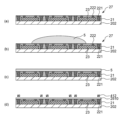
- FIG. 1 is a longitudinal cross-sectional view showing an example of an electronic device according to this embodiment.
- FIG. 2 is a partially enlarged view of the area surrounded by the chain line in FIG.
- the upper side in FIG. 1 will be referred to as “upper” and the lower side will be referred to as “lower”.
- the electronic device 1 shown in FIG. 1 has a so-called package-on-package structure including a through electrode substrate 2 and a semiconductor package 3 mounted thereon.
- the through electrode substrate 2 includes an insulating layer 21 , a plurality of through wirings 221 penetrating from the top surface to the bottom surface of the insulating layer 21 , a semiconductor chip 23 embedded inside the insulating layer 21 , and a semiconductor chip 23 provided on the bottom surface of the insulating layer 21 .
- the semiconductor package 3 includes a package substrate 31, a semiconductor chip 32 mounted on the package substrate 31, a bonding wire 33 that electrically connects the semiconductor chip 32 and the package substrate 31, and a semiconductor chip 32 and the bonding wire 33. It includes an embedded sealing layer 34 and solder bumps 35 provided on the lower surface of the package substrate 31.
- a semiconductor package 3 is stacked on the through electrode substrate 2. Thereby, the solder bumps 35 of the semiconductor package 3 and the upper wiring layer 25 of the through electrode substrate 2 are electrically connected.
- the through electrode substrate 2 and the semiconductor package 3, which are equipped with mutually different semiconductor chips, are stacked, the packaging density per unit area can be increased. Therefore, it is possible to achieve both miniaturization and high performance.
- the lower wiring layer 24 and the upper wiring layer 25 included in the through electrode substrate 2 shown in FIG. 2 each include an insulating layer, a wiring layer, a through wiring, and the like.
- the lower wiring layer 24 and the upper wiring layer 25 include wiring inside and on the surface, and are electrically connected to each other via the through wiring 221 that penetrates the insulating layer 21.
- the wiring layer included in the lower wiring layer 24 is connected to the semiconductor chip 23 and the solder bumps 26. Therefore, the lower wiring layer 24 functions as a rewiring layer of the semiconductor chip 23, and the solder bumps 26 function as external terminals of the semiconductor chip 23.
- the through wiring 221 shown in FIG. 2 is provided so as to penetrate through the insulating layer 21, as described above. Thereby, the lower wiring layer 24 and the upper wiring layer 25 are electrically connected, and the through electrode substrate 2 and the semiconductor package 3 can be stacked, so that the electronic device 1 can be highly functional. can.
- the wiring layer 253 included in the upper wiring layer 25 shown in FIG. 2 is connected to the through wiring 221 and the solder bumps 35. Therefore, the upper wiring layer 25 is electrically connected to the semiconductor chip 23 and functions as a rewiring layer for the semiconductor chip 23 and as an interposer interposed between the semiconductor chip 23 and the package substrate 31. also works.
- the cured film of the photosensitive resin composition of this embodiment can be used to constitute the insulating layer of the rewiring layer.
- the semiconductor chip 23 and the rewiring layer (upper wiring layer 25) provided on the surface of the semiconductor chip 23 are provided, and the insulating layer in the rewiring layer is the photosensitive layer of the present embodiment. It is possible to realize an electronic device composed of a cured product of a polyurethane resin composition.
- the effect of reinforcing the insulating layer 21 can be obtained. Therefore, even if the lower wiring layer 24 and the upper wiring layer 25 have low mechanical strength, the mechanical strength of the through electrode substrate 2 as a whole can be prevented from decreasing. As a result, it is possible to further reduce the thickness of the lower wiring layer 24 and the upper wiring layer 25, and it is possible to further reduce the height of the electronic device 1.
- the electronic device 1 shown in FIG. 1 also includes a through wiring 222 provided to penetrate the insulating layer 21 located on the upper surface of the semiconductor chip 23. Thereby, electrical connection between the upper surface of the semiconductor chip 23 and the upper wiring layer 25 can be achieved.
- the insulating layer 21 is provided to cover the semiconductor chip 23. This increases the effect of protecting the semiconductor chip 23. As a result, the reliability of the electronic device 1 can be improved. Moreover, the electronic device 1 can be easily applied to a mounting method such as the package-on-package structure according to the present embodiment.
- the diameter W (see FIG. 2) of the through wiring 221 is not particularly limited, but is preferably about 1 to 100 ⁇ m, more preferably about 2 to 80 ⁇ m. Thereby, the conductivity of the through wiring 221 can be ensured without impairing the mechanical properties of the insulating layer 21.
- the semiconductor package 3 shown in FIG. 1 may be any type of package.
- QFP Quad Flat Package
- SOP Small Outline Package
- BGA Bit Grid Array
- CSP Chip Size Package
- QFN Quadrature Non-leaded Package
- SON Small Outline Non-leaded Package
- forms such as LF-BGA (Lead Flame BGA).
- the arrangement of the semiconductor chips 32 is not particularly limited, but as an example, in FIG. 1, a plurality of semiconductor chips 32 are stacked. As a result, the packaging density is increased. Note that the plurality of semiconductor chips 32 may be arranged side by side in the plane direction, or may be stacked in the thickness direction and arranged side by side in the plane direction.
- the package substrate 31 may be any type of substrate, but may include, for example, an insulating layer, a wiring layer, a through wiring, etc. (not shown). Among these, the solder bumps 35 and the bonding wires 33 can be electrically connected via the through wiring.
- the sealing layer 34 is made of, for example, a known sealing resin material. By providing such a sealing layer 34, the semiconductor chip 32 and bonding wires 33 can be protected from external forces and the external environment.
- the semiconductor chip 23 included in the through electrode substrate 2 and the semiconductor chip 32 included in the semiconductor package 3 are arranged close to each other. This makes it possible to enjoy benefits such as faster mutual communication and lower loss.
- one of the semiconductor chips 23 and 32 is used as an arithmetic element such as a CPU (Central Processing Unit), a GPU (Graphics Processing Unit), or an AP (Application Processor), and the other is used as a D RAM (Dynamic Random Access
- storage elements such as memory (Memory) or flash memory, these elements can be placed close to each other in the same device. Thereby, it is possible to realize an electronic device 1 that is both highly functional and compact.
- FIG. 3 is a process diagram showing a method for manufacturing the electronic device 1 shown in FIG. 1. Further, FIGS. 4 to 6 are diagrams for explaining a method of manufacturing the electronic device 1 shown in FIG. 1, respectively.
- the manufacturing method of the electronic device 1 includes a chip placement step S1 in which the insulating layer 21 is obtained so as to embed the semiconductor chip 23 provided on the substrate 202 and the through wirings 221 and 222, and an upper layer is formed on the insulating layer 21 and the semiconductor chip 23.
- An upper wiring layer forming step S2 for forming the wiring layer 25 a substrate peeling step S3 for peeling off the substrate 202, a lower wiring layer forming step S4 for forming the lower wiring layer 24, forming the solder bumps 26, and forming the through electrode substrate. 2, and a stacking step S6 of stacking the semiconductor package 3 on the through electrode substrate 2.
- a photosensitive resin varnish 5 (varnish-like photosensitive resin composition) is placed on the insulating layer 21 and the semiconductor chip 23, and a first resin is used to form the photosensitive resin layer 2510.
- the process includes a second curing step S28 and a through wiring forming step S29 in which the through wiring 254 is formed in the opening 424 (through hole).
- Chip placement process S1 First, as shown in FIG. 4A, a chip includes a substrate 202, a semiconductor chip 23 and through wirings 221 and 222 provided on the substrate 202, and an insulating layer 21 provided to embed these. An embedded structure 27 is prepared.
- the constituent material of the substrate 202 is not particularly limited, and examples thereof include metal materials, glass materials, ceramic materials, semiconductor materials, organic materials, and the like. Furthermore, the substrate 202 may be a semiconductor wafer such as a silicon wafer, a glass wafer, or the like.
- the semiconductor chip 23 is bonded onto the substrate 202.
- a plurality of semiconductor chips 23 are placed on the same substrate 202 while being spaced apart from each other.
- the plurality of semiconductor chips 23 may be of the same type or may be of different types.
- the substrate 202 and the semiconductor chip 23 may be fixed via an adhesive layer (not shown) such as a die attach film.
- an interposer (not shown) may be provided between the substrate 202 and the semiconductor chip 23.
- the interposer functions as a rewiring layer for the semiconductor chip 23, for example. Therefore, the interposer may include pads (not shown) for electrical connection with electrodes of the semiconductor chip 23, which will be described later. Thereby, the pad spacing and arrangement pattern of the semiconductor chip 23 can be changed, and the degree of freedom in designing the electronic device 1 can be further increased.
- an inorganic substrate such as a silicon substrate, a ceramic substrate, or a glass substrate, an organic substrate such as a resin substrate, etc. are used as the interposer.
- the insulating layer 21 may be, for example, a resin film (organic insulating layer) containing a thermosetting resin or a thermoplastic resin as mentioned as a component of the photosensitive resin composition, or a general sealing layer used in the semiconductor technical field. It may also be a stopper.
- Examples of the constituent material of the through wirings 221 and 222 include copper or a copper alloy, aluminum or an aluminum alloy, gold or a gold alloy, silver or a silver alloy, nickel or a nickel alloy, and the like.
- chip-embedded structure 27 may be prepared using a method different from that described above.
- the application of the photosensitive resin varnish 5 is performed using, for example, a spin coater, a bar coater, a spray device, an inkjet device, or the like.
- the viscosity of the photosensitive resin varnish 5 is not particularly limited, but is 10 cP to 6000 cP, preferably 20 cP to 5000 cP, and more preferably 30 cP to 4000 cP.
- a thinner photosensitive resin layer 2510 (see FIG. 4(d)) can be formed.
- the upper wiring layer 25 can be made thinner, making it easier to make the electronic device 1 thinner.
- the viscosity of the photosensitive resin varnish 5 is, for example, a value measured using a cone-plate viscometer (TV-25, manufactured by Toki Sangyo Co., Ltd.) at a rotation speed of 100 rpm.
- the drying conditions for the photosensitive resin varnish 5 are not particularly limited, but include, for example, heating at a temperature of 80 to 150° C. for 1 to 60 minutes.
- the photosensitive resin film is a photosensitive resin composition of this embodiment, and is a resin film having photosensitivity.
- the photosensitive resin film is manufactured, for example, by applying the photosensitive resin varnish 5 onto a base such as a carrier film using various coating devices, and then drying the resulting coating film.
- the photosensitive resin layer 2510 is subjected to pre-exposure heat treatment, if necessary.
- pre-exposure heat treatment By performing the pre-exposure heat treatment, the molecules contained in the photosensitive resin layer 2510 are stabilized, and the reaction in the first exposure step S21 described later can be stabilized.
- the adverse effects of heating on the photoacid generator can be minimized.
- the temperature of the pre-exposure heat treatment is preferably 70 to 130°C, more preferably 75 to 120°C, and even more preferably 80 to 110°C. If the temperature of the pre-exposure heat treatment is below the lower limit, there is a possibility that the purpose of stabilizing molecules by the pre-exposure heat treatment will not be achieved. On the other hand, if the temperature of the pre-exposure heat treatment exceeds the upper limit, the movement of the photoacid generator becomes too active, resulting in the effect that it becomes difficult to generate acid even when light is irradiated in the first exposure step S21, which will be described later. There is a possibility that the patterning accuracy will decrease due to the wide range of patterning.
- the time of the pre-exposure heat treatment is appropriately set depending on the temperature of the pre-exposure heat treatment, but at the above temperature it is preferably 1 to 10 minutes, more preferably 2 to 8 minutes, still more preferably 3 to 8 minutes. It is said to be 6 minutes. If the time for the pre-exposure heat treatment is less than the lower limit, the heating time will be insufficient, and there is a risk that the purpose of the pre-exposure heat treatment, which is stabilization of molecules, will not be achieved. On the other hand, if the pre-exposure heat treatment time exceeds the above upper limit, the heating time will be too long and the action of the photoacid generator will be inhibited even if the pre-exposure heat treatment temperature is within the above range. There is a risk of it getting lost.
- the atmosphere for the heat treatment is not particularly limited. Although an inert gas atmosphere, a reducing gas atmosphere, etc. may be used, in consideration of work efficiency, etc., it is preferable to use the atmosphere.
- the atmospheric pressure is not particularly limited. It may be under reduced pressure or increased pressure, but in consideration of work efficiency etc., normal pressure is used. Note that normal pressure refers to a pressure of about 30 to 150 kPa, preferably atmospheric pressure.
- a mask 412 is placed in a predetermined area on the photosensitive resin layer 2510. Then, light (active radiation) is irradiated through the mask 412. Thereby, exposure processing is performed on the photosensitive resin layer 2510 according to the pattern of the mask 412.
- FIG. 4(d) shows a case where the photosensitive resin layer 2510 has so-called negative photosensitivity.
- a region of the photosensitive resin layer 2510 corresponding to the light-blocking portion of the mask 412 is dissolved in the developer.
- active chemical species are generated from the photocationic polymerization initiator.
- the active species acts as a catalyst for the curing reaction.
- the amount of exposure in the exposure process is not particularly limited. 100 to 2000 mJ/cm 2 is preferable, and 200 to 1000 mJ/cm 2 is more preferable. Thereby, underexposure and overexposure in the photosensitive resin layer 2510 can be suppressed. As a result, high patterning accuracy can finally be achieved. Thereafter, if necessary, the photosensitive resin layer 2510 is subjected to post-exposure heat treatment.
- the temperature of the post-exposure heat treatment is not particularly limited.
- the temperature is preferably 50 to 150°C, more preferably 50 to 130°C, even more preferably 55 to 120°C, particularly preferably 60 to 110°C.
- the time for the post-exposure heat treatment is appropriately set depending on the temperature of the post-exposure heat treatment.
- the heating time is preferably 1 to 30 minutes, more preferably 2 to 20 minutes, and even more preferably 3 to 15 minutes.
- the atmosphere for the post-exposure heat treatment is not particularly limited. Although an inert gas atmosphere, a reducing gas atmosphere, etc. may be used, in consideration of work efficiency, etc., it is preferable to use the atmosphere.
- the atmospheric pressure of the post-exposure heat treatment is not particularly limited. It may be under reduced pressure or increased pressure, but in consideration of work efficiency etc., normal pressure is used. Thereby, the pre-exposure heat treatment can be performed relatively easily.
- normal pressure refers to a pressure of about 30 to 150 kPa, preferably atmospheric pressure.
- the developer examples include an organic solvent developer, a water-soluble developer, and the like.
- the developer preferably contains an organic solvent. More specifically, the developer is preferably a developer containing an organic solvent as a main component (a developer in which 95% by mass or more of the components is an organic solvent). By developing with a developer containing an organic solvent, swelling of the pattern due to the developer can be suppressed more than when developing with an alkaline developer (aqueous). In other words, it is easier to obtain a finer pattern.
- organic solvents that can be used in the developer include ketone solvents such as cyclopentanone, ester solvents such as propylene glycol monomethyl ether acetate (PGMEA) and butyl acetate, ether solvents such as propylene glycol monomethyl ether, etc.
- an organic solvent developer may be used, which consists only of an organic solvent and does not contain any impurities other than unavoidable impurities. Impurities that are unavoidably included include metal elements and water, but from the viewpoint of preventing contamination of electronic devices, it is better to have fewer impurities that are unavoidably included.
- the method of bringing the developer into contact with the photosensitive resin layer 2510 is not particularly limited. Generally known methods such as a dipping method, a paddle method, and a spray method can be applied as appropriate.
- the time for the development step is usually about 5 to 300 seconds, preferably about 10 to 120 seconds, and is adjusted as appropriate based on the thickness of the resin film, the shape of the pattern to be formed, etc.
- the photosensitive resin layer 2510 is subjected to a curing process (post-development heat treatment).
- the conditions of the curing treatment are not particularly limited, but the heating temperature is about 160 to 250° C. and the heating time is about 30 to 240 minutes. Thereby, the photosensitive resin layer 2510 can be cured and the organic insulating layer 251 can be obtained while suppressing the thermal influence on the semiconductor chip 23.
- Wiring layer forming step S24 Next, a wiring layer 253 is formed on the organic insulating layer 251 (see FIG. 5(f)).
- the wiring layer 253 is formed by obtaining a metal layer using a vapor phase film forming method such as a sputtering method or a vacuum evaporation method, and then patterning the metal layer using a photolithography method and an etching method. Prior to forming the wiring layer 253, surface modification treatment such as plasma treatment may be performed.
- a photosensitive resin layer 2520 is obtained in the same manner as in the first resin film arrangement step S20.
- the photosensitive resin layer 2520 is arranged to cover the wiring layer 253. Thereafter, if necessary, the photosensitive resin layer 2520 is subjected to pre-exposure heat treatment.
- the processing conditions are, for example, the conditions described in the first resin film placement step S20.
- Second exposure step S26 Next, the photosensitive resin layer 2520 is exposed to light.
- the processing conditions are, for example, the conditions described in the first exposure step S21. Thereafter, the photosensitive resin layer 2520 is subjected to post-exposure heat treatment, if necessary.
- the processing conditions are, for example, the conditions described in the first exposure step S21.
- Second development step S27 the photosensitive resin layer 2520 is subjected to a development process.
- the processing conditions are, for example, the conditions described in the first development step S22.
- an opening 424 passing through the photosensitive resin layers 2510 and 2520 is formed (see FIG. 5(h)).
- Second curing step S28 After the development process, the photosensitive resin layer 2520 is subjected to a curing process (post-development heat treatment).
- the curing conditions are, for example, the conditions described in the first curing step S23. Thereby, the photosensitive resin layer 2520 is cured, and an organic insulating layer 252 is obtained (see FIG. 6(i)).
- the upper wiring layer 25 has two layers, the organic insulating layer 251 and the organic insulating layer 252, but it may have three or more layers. In this case, after the second curing step S28, a series of steps from the wiring layer forming step S24 to the second curing step S28 may be repeatedly added.
- a known method is used to form the through wiring 254, and for example, the following method is used.
- a seed layer (not shown) is formed on the organic insulating layer 252.
- the seed layer is formed on the inner surface (side surface and bottom surface) of the opening 424 as well as on the upper surface of the organic insulating layer 252.
- a copper seed layer is used as the seed layer.
- the seed layer is formed by, for example, a sputtering method.
- the seed layer may be made of the same type of metal as the through wiring 254 to be formed, or may be made of a different type of metal.
- a resist layer (not shown) is formed on a region other than the opening 424 of the seed layer (not shown). Then, using this resist layer as a mask, the opening 424 is filled with metal. For example, electrolytic plating is used for this filling. Examples of the metal to be filled include copper or a copper alloy, aluminum or an aluminum alloy, gold or a gold alloy, silver or a silver alloy, nickel or a nickel alloy. In this way, the conductive material is buried in the opening 424, and the through wiring 254 is formed.
- the resist layer (not shown) is removed. Furthermore, the seed layer (not shown) on the organic insulating layer 252 is removed. For this purpose, for example, a flash etching method can be used.
- the location where the through wiring 254 is formed is not limited to the illustrated position.
- Lower wiring layer forming step S4 Next, as shown in FIG. 6(k), a lower wiring layer 24 is formed on the lower surface side of the insulating layer 21.
- the lower wiring layer 24 may be formed by any method, for example, in the same manner as the upper wiring layer forming step S2 described above.
- the lower wiring layer 24 formed in this way is electrically connected to the upper wiring layer 25 via the through wiring 221.
- solder bump forming step S5 As shown in FIG. 6(L), solder bumps 26 are formed on the lower wiring layer 24. Further, a protective film such as a solder resist layer may be formed on the upper wiring layer 25 and the lower wiring layer 24 as necessary. In the manner described above, the through electrode substrate 2 is obtained.
- the through electrode substrate 2 shown in FIG. 6(L) can be divided into a plurality of regions. Therefore, for example, by dividing the through electrode substrate 2 into pieces along the dashed line shown in FIG. 6(L), a plurality of through electrode substrates 2 can be efficiently manufactured. Note that, for example, a diamond cutter or the like can be used to separate the pieces into pieces.
- Such a method of manufacturing the electronic device 1 can be applied to a wafer level process or a panel level process using a large-area substrate. Thereby, manufacturing efficiency of the electronic device 1 can be increased and costs can be reduced.
- the imidization rate of the resin analyzed by 1 H-NMR was 95% or more.
- the weight average molecular weight (Mw) is determined by GPC (Gel Permeation Chromatography) measurement of polyimide resin using THF as a solvent at a measurement temperature of 40°C and a sample concentration of 0.5 wt%, and then by GPC measurement under the same conditions. It was determined using the polystyrene equivalent value calculated from the standard polystyrene (PS) calibration curve obtained by.
- the imidization rate is determined by measuring the 1 H-NMR spectrum of the polyimide resin.
- the area of the peak corresponding to the amide group is A AM
- the area of the peak corresponding to the imide ring group is A AM
- IM it was calculated using the formula ⁇ A IM /(A IM +A AM ) ⁇ 100(%).
- ⁇ Synthesis of polyimide precursor resin (A-4)> Put 428 g of ⁇ -butyrolactone, 155.11 g of 4,4'-oxydiphthalic dianhydride, and 130.14 g of 2-hydroxyethyl methacrylate into a 2 L separable flask, and stir the components in the flask at room temperature to completely dissolve them. Ta. Subsequently, 79.1 g of pyridine was added while stirring at room temperature, and the mixture was further stirred at room temperature for 16 hours.
- Resin (A-4) had a weight average molecular weight (Mw) of 30,000 as measured by GPC. Furthermore, the imidization rate of the resin analyzed by 1 H-NMR was less than 5%.
- the water content (mass%) in the varnish is the water content in the varnish that includes all the water added as raw materials during formulation, the water contained in the silane coupling agent (C-1), and the water mixed during composition preparation.
- the amount is a value measured using a Karl Fischer moisture meter.
- A-1) Polyimide resin having an imide ring structure synthesized above (A-1)
- A-2) Polyimide resin having an imide ring structure synthesized above (A-2)
- A-3) Polyimide resin having an imide ring structure synthesized above (A-3)
- A-4) Polyimide precursor synthesized above ⁇ for comparative example>
- A-5) Polyimide resin having an imide ring structure synthesized above (A-5)
- D-1 NK ester A-9550 (manufactured by Shin Nakamura Chemical Co., Ltd., dipentaerythritol polyacrylate, compound having 5 to 6 acryloyl groups in one molecule)
- D-2) Viscoat #230 (manufactured by Osaka Organic Chemical Industry Co., Ltd., a compound having two acryloyl groups in one molecule)
- G-1 Ethyl lactate (EL)
- G-2 Gamma-butyrolactone (GBL)
- the obtained photosensitive resin composition was evaluated based on the items listed in Table 1. Note that in Table 1, "-" means that no evaluation was performed.
- the mass of water generated from the photosensitive resin composition ( mg) was measured according to the volumetric titration method specified in JIS K 0113:2005. Next, the water content was determined when the total amount of the photosensitive resin composition (varnish) was 100% by mass, and was defined as the water content (mass%).
- ⁇ Adhesion 90 degree peel strength> (Creation of substrate for 90 degree peel strength evaluation)
- the obtained photosensitive resin composition was spin-coated onto a 12-inch silicon wafer having a 3000 ⁇ plated copper layer on its surface to a dry film thickness of 10 ⁇ m, and then coated at 120° C. for 3 minutes.
- a photosensitive resin film was obtained by heating.
- the obtained photosensitive resin film was exposed to 300 mJ/cm 2 using an i-line stepper through a photomask so that a range of 6.5 mm in width and 50 mm in length was exposed.
- the exposed resin film was developed with cyclopentanone and propylene glycol monomethyl ether acetate together with the silicon wafer using a spray developing machine, and then air-dried using a spin dryer and then dried on a hot plate at 120°C for 2 minutes. went. Furthermore, after that, heat treatment was performed at 200° C. for 90 minutes in a nitrogen atmosphere to obtain a cured film. Subsequently, the silicon wafer was cut so that the obtained cured film with a width of 6.5 mm and a length of 50 mm remained, and the end portion (5 mm) of the cured film was immersed in a 2% hydrofluoric acid aqueous solution at 23 ° C. for 6 hours. The substrate was washed with water and dried to obtain a substrate for evaluation of 90 degree peel strength from which the film at the edges was peeled off.
- the unit of 90 degree peel strength is N/cm. A higher 90 degree peel strength is preferable from the viewpoint of reliability.
- the obtained photosensitive resin composition was spin-coated onto a 12-inch silicon wafer with a 3000 ⁇ plated copper layer on the surface to a dry film thickness of 5 ⁇ m, and dried on a hot plate at 120° C. for 3 minutes.
- a photosensitive resin film was obtained.
- the i-line stepper manufactured by CANON, FPA-5500iX ), the i-line was irradiated while changing the exposure amount.
- the exposed film was developed using a spray developer using cyclopentanone at 2500 rpm for 30 seconds, then developed using propylene glycol monomethyl ether acetate at 2500 rpm for 10 seconds, and then spin-dried at 2500 rpm for 10 seconds.
- ⁇ Normal temperature viscosity change rate> The viscosity of the photosensitive resin composition immediately after blending was measured using an E-type viscometer (TVE-25L). The viscosity at this time was designated as A. Thereafter, the varnish of the photosensitive resin composition used to measure the viscosity A was stored at 23° C. for 7 days, and the viscosity was measured again. The viscosity at this time was designated as B. Using the values of viscosity A and viscosity B, "viscosity change rate" was calculated based on the following formula.
- Viscosity change rate [%] ⁇ (viscosity A - viscosity B)/viscosity A ⁇ x 100
- the obtained cured product was cut with a dicing saw along with the silicon wafer to a width of 5 mm, and then peeled off from the substrate by immersing it in a 2% by mass hydrofluoric acid aqueous solution.
- the peeled film was dried at 60° C. for 10 hours to obtain a test piece (30 mm x 5 mm x 10 ⁇ m thick).
- Tg glass transition temperature
- the exposed resin film was developed with cyclopentanone and propylene glycol monomethyl ether acetate together with the silicon wafer using a spray developing machine, and then air-dried using a spin dryer and then dried on a hot plate at 140°C for 2 minutes. went. Furthermore, after that, heat treatment was performed at 200° C. for 120 minutes in a nitrogen atmosphere to obtain a resin film.
- the obtained resin film was peeled from the substrate by immersing it in a 2% by mass hydrofluoric acid aqueous solution, washed with water, and then dried at 60°C for 10 hours to obtain a test piece for measurement (50 mm x 5 mm x 10 ⁇ m thick). .
- the measurement test piece obtained in the above was tested in accordance with JIS K 7161 in an atmosphere of 23°C using a tensile tester (manufactured by Orientech, Tensilon RTC-1210A). A tensile test was conducted in accordance with the method, and the tensile elongation rate of the test piece was measured. The stretching speed in the tensile test was 5 mm/min. The unit of tensile elongation is %.
- the photosensitive resin compositions of Examples 1 to 6 have a smaller room temperature viscosity change rate than Comparative Example 1, and have a better varnish appearance than Comparative Example 3, so they have excellent storage stability. Since the number of 90 degree peel strength fluctuations was smaller than that of Sample No. 2, the result showed that excellent copper adhesion stability was exhibited.
- the photosensitive resin compositions of Examples 7 to 9 have a smaller room-temperature viscosity change rate than Comparative Example 1, and have a better varnish appearance than Comparative Example 3, so they have excellent storage stability. Compared to Comparative Examples 2 and 4, the number of changes in 90 degree peel strength was smaller, indicating excellent copper adhesion stability.
Landscapes
- Physics & Mathematics (AREA)
- General Physics & Mathematics (AREA)
- Spectroscopy & Molecular Physics (AREA)
- Materials For Photolithography (AREA)
- Macromolecular Compounds Obtained By Forming Nitrogen-Containing Linkages In General (AREA)
- Compositions Of Macromolecular Compounds (AREA)
- Polymerisation Methods In General (AREA)
Priority Applications (2)
| Application Number | Priority Date | Filing Date | Title |
|---|---|---|---|
| JP2024503915A JP7505659B1 (ja) | 2022-09-08 | 2023-08-31 | 感光性樹脂組成物、樹脂膜、および電子装置 |
| KR1020257010728A KR20250060263A (ko) | 2022-09-08 | 2023-08-31 | 감광성 수지 조성물, 수지막, 및 전자 장치 |
Applications Claiming Priority (2)
| Application Number | Priority Date | Filing Date | Title |
|---|---|---|---|
| JP2022-142797 | 2022-09-08 | ||
| JP2022142797 | 2022-09-08 |
Publications (1)
| Publication Number | Publication Date |
|---|---|
| WO2024053564A1 true WO2024053564A1 (ja) | 2024-03-14 |
Family
ID=90191064
Family Applications (1)
| Application Number | Title | Priority Date | Filing Date |
|---|---|---|---|
| PCT/JP2023/031925 Ceased WO2024053564A1 (ja) | 2022-09-08 | 2023-08-31 | 感光性樹脂組成物、樹脂膜、および電子装置 |
Country Status (4)
| Country | Link |
|---|---|
| JP (1) | JP7505659B1 (https=) |
| KR (1) | KR20250060263A (https=) |
| TW (1) | TW202419528A (https=) |
| WO (1) | WO2024053564A1 (https=) |
Citations (3)
| Publication number | Priority date | Publication date | Assignee | Title |
|---|---|---|---|---|
| JP2021162834A (ja) * | 2020-03-31 | 2021-10-11 | 住友ベークライト株式会社 | 感光性樹脂組成物、電子デバイスの製造方法および電子デバイス |
| JP2022019609A (ja) * | 2020-07-16 | 2022-01-27 | 住友ベークライト株式会社 | 感光性樹脂組成物、電子デバイスの製造方法、電子デバイスおよび感光性樹脂組成物の製造方法 |
| WO2022145136A1 (ja) * | 2020-12-28 | 2022-07-07 | 富士フイルム株式会社 | 樹脂組成物、硬化物、積層体、硬化物の製造方法、及び、半導体デバイス、並びに、化合物 |
Family Cites Families (5)
| Publication number | Priority date | Publication date | Assignee | Title |
|---|---|---|---|---|
| JP5620691B2 (ja) * | 2010-02-16 | 2014-11-05 | 旭化成イーマテリアルズ株式会社 | 感光性樹脂組成物、硬化レリーフパターンの製造方法、並びに半導体装置 |
| JP5762706B2 (ja) * | 2010-09-06 | 2015-08-12 | 旭化成イーマテリアルズ株式会社 | 感光性樹脂組成物及び硬化レリーフパターンの製造方法 |
| JP2018070829A (ja) | 2016-11-02 | 2018-05-10 | 東レ株式会社 | 樹脂組成物 |
| JP7062899B2 (ja) * | 2017-09-15 | 2022-05-09 | 住友ベークライト株式会社 | 感光性樹脂組成物、半導体装置および電子機器 |
| JP7392580B2 (ja) * | 2020-06-08 | 2023-12-06 | 住友ベークライト株式会社 | 感光性樹脂組成物、電子デバイスの製造方法および電子デバイス |
-
2023
- 2023-08-31 WO PCT/JP2023/031925 patent/WO2024053564A1/ja not_active Ceased
- 2023-08-31 KR KR1020257010728A patent/KR20250060263A/ko active Pending
- 2023-08-31 JP JP2024503915A patent/JP7505659B1/ja active Active
- 2023-09-04 TW TW112133469A patent/TW202419528A/zh unknown
Patent Citations (3)
| Publication number | Priority date | Publication date | Assignee | Title |
|---|---|---|---|---|
| JP2021162834A (ja) * | 2020-03-31 | 2021-10-11 | 住友ベークライト株式会社 | 感光性樹脂組成物、電子デバイスの製造方法および電子デバイス |
| JP2022019609A (ja) * | 2020-07-16 | 2022-01-27 | 住友ベークライト株式会社 | 感光性樹脂組成物、電子デバイスの製造方法、電子デバイスおよび感光性樹脂組成物の製造方法 |
| WO2022145136A1 (ja) * | 2020-12-28 | 2022-07-07 | 富士フイルム株式会社 | 樹脂組成物、硬化物、積層体、硬化物の製造方法、及び、半導体デバイス、並びに、化合物 |
Also Published As
| Publication number | Publication date |
|---|---|
| KR20250060263A (ko) | 2025-05-07 |
| TW202419528A (zh) | 2024-05-16 |
| JPWO2024053564A1 (https=) | 2024-03-14 |
| JP7505659B1 (ja) | 2024-06-25 |
Similar Documents
| Publication | Publication Date | Title |
|---|---|---|
| JP7840247B2 (ja) | 電子デバイスの製造方法 | |
| TW201817778A (zh) | 聚醯亞胺前驅體、含有該聚醯亞胺前驅體的感光性樹脂組成物、使用其的圖案硬化膜的製造方法、硬化膜、圖案硬化膜及半導體裝置 | |
| JP7592393B2 (ja) | ネガ型感光性樹脂組成物、ポリイミドの製造方法および硬化レリーフパターンの製造方法 | |
| JP7135864B2 (ja) | 半導体装置の製造方法 | |
| JP2018146964A (ja) | 感光性樹脂組成物、パターン硬化物の製造方法、硬化物、層間絶縁膜、カバーコート層、表面保護膜及び電子部品 | |
| JP2024024808A (ja) | 感光性樹脂組成物、電子デバイスの製造方法および電子デバイス | |
| JP2025083394A (ja) | 感光性樹脂組成物、電子デバイスの製造方法および電子デバイス | |
| JP7505659B1 (ja) | 感光性樹脂組成物、樹脂膜、および電子装置 | |
| WO2022270544A1 (ja) | ネガ型感光性樹脂組成物、ネガ型感光性ポリマー、硬化膜および半導体装置 | |
| JP2022019609A (ja) | 感光性樹脂組成物、電子デバイスの製造方法、電子デバイスおよび感光性樹脂組成物の製造方法 | |
| JP2011195736A (ja) | ポリイミド前駆体及び感光性樹脂組成物 | |
| KR102921834B1 (ko) | 감광성 수지 조성물, 전자 디바이스의 제조 방법 및 전자 디바이스 | |
| JP2024038631A (ja) | 感光性樹脂組成物、樹脂膜、および電子装置 | |
| JP2024038630A (ja) | 感光性樹脂組成物、電子デバイスの製造方法および電子デバイス | |
| WO2018179330A1 (ja) | 感光性樹脂組成物、パターン硬化膜の製造方法、硬化物、層間絶縁膜、カバーコート層、表面保護膜、及び電子部品 | |
| JP7507311B2 (ja) | 感光性樹脂組成物、電子デバイスの製造方法、電子デバイスおよび光デバイス | |
| WO2022202907A1 (ja) | 感光性樹脂組成物、樹脂膜および電子装置 | |
| JP2024003100A (ja) | 感光性樹脂組成物 | |
| WO2023021684A1 (ja) | 感光性樹脂組成物、電子デバイスの製造方法および電子デバイス | |
| JP6707854B2 (ja) | ポジ型感光性樹脂組成物、硬化膜、保護膜、絶縁膜および電子装置 | |
| TW202309150A (zh) | 感光性樹脂組成物、電子裝置之製造方法及電子裝置 | |
| JP7494462B2 (ja) | 感光性樹脂組成物、電子デバイスの製造方法および電子デバイス | |
| JP7375406B2 (ja) | 感光性樹脂組成物、電子デバイスの製造方法および電子デバイス | |
| TWI908861B (zh) | 感光性樹脂組成物、電子裝置之製造方法及電子裝置 | |
| JP2023138254A (ja) | 感光性樹脂組成物、電子デバイスおよびその製造方法 |
Legal Events
| Date | Code | Title | Description |
|---|---|---|---|
| ENP | Entry into the national phase |
Ref document number: 2024503915 Country of ref document: JP Kind code of ref document: A |
|
| 121 | Ep: the epo has been informed by wipo that ep was designated in this application |
Ref document number: 23863102 Country of ref document: EP Kind code of ref document: A1 |
|
| ENP | Entry into the national phase |
Ref document number: 20257010728 Country of ref document: KR Kind code of ref document: A |
|
| WWE | Wipo information: entry into national phase |
Ref document number: 1020257010728 Country of ref document: KR |
|
| NENP | Non-entry into the national phase |
Ref country code: DE |
|
| 122 | Ep: pct application non-entry in european phase |
Ref document number: 23863102 Country of ref document: EP Kind code of ref document: A1 |