WO2024024371A1 - 半導体装置 - Google Patents
半導体装置 Download PDFInfo
- Publication number
- WO2024024371A1 WO2024024371A1 PCT/JP2023/023816 JP2023023816W WO2024024371A1 WO 2024024371 A1 WO2024024371 A1 WO 2024024371A1 JP 2023023816 W JP2023023816 W JP 2023023816W WO 2024024371 A1 WO2024024371 A1 WO 2024024371A1
- Authority
- WO
- WIPO (PCT)
- Prior art keywords
- layer
- conductive
- semiconductor device
- coating
- bonding
- Prior art date
- Legal status (The legal status is an assumption and is not a legal conclusion. Google has not performed a legal analysis and makes no representation as to the accuracy of the status listed.)
- Ceased
Links
Images


Classifications
-
- H—ELECTRICITY
- H10—SEMICONDUCTOR DEVICES; ELECTRIC SOLID-STATE DEVICES NOT OTHERWISE PROVIDED FOR
- H10W—GENERIC PACKAGES, INTERCONNECTIONS, CONNECTORS OR OTHER CONSTRUCTIONAL DETAILS OF DEVICES COVERED BY CLASS H10
- H10W40/00—Arrangements for thermal protection or thermal control
- H10W40/10—Arrangements for heating
-
- H—ELECTRICITY
- H10—SEMICONDUCTOR DEVICES; ELECTRIC SOLID-STATE DEVICES NOT OTHERWISE PROVIDED FOR
- H10W—GENERIC PACKAGES, INTERCONNECTIONS, CONNECTORS OR OTHER CONSTRUCTIONAL DETAILS OF DEVICES COVERED BY CLASS H10
- H10W40/00—Arrangements for thermal protection or thermal control
- H10W40/20—Arrangements for cooling
- H10W40/25—Arrangements for cooling characterised by their materials
- H10W40/255—Arrangements for cooling characterised by their materials having a laminate or multilayered structure, e.g. direct bond copper [DBC] ceramic substrates
-
- H—ELECTRICITY
- H10—SEMICONDUCTOR DEVICES; ELECTRIC SOLID-STATE DEVICES NOT OTHERWISE PROVIDED FOR
- H10W—GENERIC PACKAGES, INTERCONNECTIONS, CONNECTORS OR OTHER CONSTRUCTIONAL DETAILS OF DEVICES COVERED BY CLASS H10
- H10W70/00—Package substrates; Interposers; Redistribution layers [RDL]
- H10W70/60—Insulating or insulated package substrates; Interposers; Redistribution layers
- H10W70/611—Insulating or insulated package substrates; Interposers; Redistribution layers for connecting multiple chips together
-
- H—ELECTRICITY
- H10—SEMICONDUCTOR DEVICES; ELECTRIC SOLID-STATE DEVICES NOT OTHERWISE PROVIDED FOR
- H10W—GENERIC PACKAGES, INTERCONNECTIONS, CONNECTORS OR OTHER CONSTRUCTIONAL DETAILS OF DEVICES COVERED BY CLASS H10
- H10W70/00—Package substrates; Interposers; Redistribution layers [RDL]
- H10W70/60—Insulating or insulated package substrates; Interposers; Redistribution layers
- H10W70/62—Insulating or insulated package substrates; Interposers; Redistribution layers characterised by their interconnections
- H10W70/66—Conductive materials thereof
-
- H—ELECTRICITY
- H10—SEMICONDUCTOR DEVICES; ELECTRIC SOLID-STATE DEVICES NOT OTHERWISE PROVIDED FOR
- H10W—GENERIC PACKAGES, INTERCONNECTIONS, CONNECTORS OR OTHER CONSTRUCTIONAL DETAILS OF DEVICES COVERED BY CLASS H10
- H10W90/00—Package configurations
-
- H—ELECTRICITY
- H10—SEMICONDUCTOR DEVICES; ELECTRIC SOLID-STATE DEVICES NOT OTHERWISE PROVIDED FOR
- H10W—GENERIC PACKAGES, INTERCONNECTIONS, CONNECTORS OR OTHER CONSTRUCTIONAL DETAILS OF DEVICES COVERED BY CLASS H10
- H10W90/00—Package configurations
- H10W90/811—Multiple chips on leadframes
Definitions
- the present disclosure relates to a semiconductor device.
- Patent Document 1 discloses an example of a semiconductor device including a circuit layer and a semiconductor element conductively bonded to the circuit layer.
- the circuit layer includes a first layer and a second layer joined to the first layer by solid state bonding.
- the first layer is bonded to the ceramic substrate.
- An object of the present disclosure is to provide a semiconductor device that is improved over the conventional semiconductor device.
- one object of the present disclosure is to provide a semiconductor device that can improve the heat dissipation of the device by further strengthening the bonding state between the support layer and the conductive layer. shall be.
- a semiconductor device includes a support layer, a conductive layer bonded to the support layer, a conductive layer located on the opposite side of the support layer with respect to the conductive layer, and a first covering layer located between the supporting layer and the conductive layer and covering the supporting layer; a first covering layer located between the first covering layer and the conductive layer; and a second coating layer that covers the conductive layer, and a bonding layer that bonds the first coating layer and the second coating layer.
- the bonding layer includes a base layer, a third coating layer located between the base layer and the first coating layer, and a fourth coating layer located between the base layer and the second coating layer.
- a solid phase bonding layer is formed between the first coating layer and the third coating layer, and between the second coating layer and the fourth coating layer.
- the Vickers hardness of the base layer is smaller than the Vickers hardness of each of the support layer and the conductive layer.
- Each of the third coating layer and the fourth coating layer includes a first layer that covers the base layer, a second layer that covers the first layer, and a third layer that covers the second layer.
- the degree of diffusion of the second layer into each of the third layer, the first coating layer, and the second coating layer is determined by the degree of diffusion of the second layer into each of the third layer, the first coating layer, and the second coating layer. This is greater than the degree of diffusion in the first layer.
- the bonding state between the support layer and the conductive layer becomes stronger, so it is possible to improve the heat dissipation performance of the semiconductor device.
- FIG. 1 is a perspective view of a semiconductor device according to a first embodiment of the present disclosure.
- FIG. 2 is a plan view of the semiconductor device shown in FIG. 1.
- FIG. 3 is a plan view corresponding to FIG. 2, in which the sealing resin is seen through.
- FIG. 4 is a partially enlarged view of FIG. 3.
- FIG. 5 is a plan view corresponding to FIG. 2, in which the first conductive member is seen through, and illustration of the sealing resin and the second conductive member is omitted.
- FIG. 6 is a right side view of the semiconductor device shown in FIG. 1.
- 7 is a bottom view of the semiconductor device shown in FIG. 1.
- FIG. 8 is a cross-sectional view taken along line VIII-VIII in FIG. 3.
- FIG. 9 is a cross-sectional view taken along line IX-IX in FIG. 3.
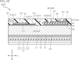
- FIG. 10 is a partially enlarged view of the first element shown in FIG. 9 and its surroundings.
- FIG. 11 is a partially enlarged view of the second element shown in FIG. 9 and its surroundings.
- FIG. 12 is a sectional view taken along line XII-XII in FIG. 3.
- FIG. 13 is a cross-sectional view taken along line XIII-XIII in FIG.
- FIG. 14 is a partially enlarged view of FIG. 10.
- FIG. 15 is a partially enlarged cross-sectional view of a semiconductor device according to a second embodiment of the present disclosure.
- FIG. 16 is a plan view of a semiconductor device according to a third embodiment of the present disclosure, in which the first conductive member is seen through and illustration of the sealing resin and the second conductive member is omitted.
- FIG. 17 is a cross-sectional view taken along line XVII-XVII in FIG. 16.
- FIG. 18 is a cross-sectional view taken along line XVIII-XVIII in FIG. 16.
- FIG. 19 is a cross-sectional view taken along line XIX-XIX in FIG. 16.
- FIG. 20 is a plan view of a semiconductor device according to a fourth embodiment of the present disclosure, in which the first conductive member is seen through, and the sealing resin and the second conductive member are not illustrated.
- FIG. 20 is a plan view of a semiconductor device according to a fourth embodiment of the present disclosure, in which the first conductive member is seen through, and the sealing resin and the second conductive member are not illustrated.
- FIG. 21 is a cross-sectional view taken along line XXI-XXI in FIG. 20.
- 22 is a cross-sectional view taken along line XXII-XXII in FIG. 20.
- FIG. 23 is a cross-sectional view taken along line XXIII-XXIII in FIG. 20.
- the semiconductor device A10 includes a base material 11, two conductive layers 12, two first coating layers 71, two second coating layers 72, two bonding layers 73, a first input terminal 13, an output terminal 14, and a second input terminal. It includes a terminal 15, a plurality of semiconductor elements 21, a first conductive member 31, a second conductive member 32, and a sealing resin 50. Further, the semiconductor device A10 includes a first signal terminal 161, a second signal terminal 162, a third signal terminal 171, a fourth signal terminal 172, two fifth signal terminals 181, two sixth signal terminals 182, and a seventh signal terminal. 19, two thermistors 22, and two control wires 60.
- the sealing resin 50 is shown for convenience of understanding.
- the transparent sealing resin 50 is shown by an imaginary line (two-dot chain line).
- the light passes through the first conductive member 31, and illustration of the second conductive member 32 and the sealing resin 50 is omitted.
- the transparent first conductive member 31 is shown by an imaginary line.
- first direction z An example of a direction perpendicular to the first direction z is referred to as a "second direction x.”
- second direction x An example of a direction perpendicular to the first direction z and the second direction x is referred to as a "third direction y.”
- "viewed in the first direction z" corresponds to "planar view”.
- the semiconductor device A10 converts the DC power supply voltage applied to the first input terminal 13 and the second input terminal 15 into AC power using the semiconductor element 21.
- the converted AC power is input from the output terminal 14 to a power supply target such as a motor.
- the base material 11 is located on the opposite side of the plurality of semiconductor elements 21 with respect to the two conductive layers 12 in the first direction z.
- Base material 11 supports two conductive layers 12 .
- the base material 11 is obtained from, for example, a DBC (Direct Bonded Copper) substrate.
- the base material 11 includes an insulating layer 111, two support layers 112, and a heat dissipation layer 113.
- the base material 11 is covered with a sealing resin 50 except for a part of the heat dissipation layer 113.
- the insulating layer 111 is located on the opposite side of the two conductive layers 12 with respect to the two support layers 112 in the first direction z.
- the insulating layer 111 is made of a material with higher thermal conductivity.
- the insulating layer 111 is, for example, a ceramic plate containing aluminum nitride (AlN).
- AlN aluminum nitride
- the insulating layer 111 may be an insulating resin sheet containing a filler having higher thermal conductivity.
- the thickness of the insulating layer 111 is smaller than the thickness of each of the two conductive layers 12. In this disclosure, the dimension in the first direction z is referred to as "thickness.”
- the two support layers 112 are located between the insulating layer 111 and the two conductive layers 12.
- the two support layers 112 are separated from each other in the second direction x.
- the two support layers 112 are bonded to the insulating layer 111.
- the two support layers 112 contain copper (Cu).
- each of the two support layers 112 is surrounded by a peripheral edge 111A of the insulating layer 111 when viewed in the first direction z.
- the heat dissipation layer 113 is located on the opposite side of the two support layers 112 with respect to the insulating layer 111.
- the heat dissipation layer 113 is bonded to the insulating layer 111.
- Heat dissipation layer 113 contains copper.
- the heat dissipation layer 113 is exposed to the outside from the sealing resin 50.
- the thickness of the heat dissipation layer 113 is greater than the thickness of the insulating layer 111.
- the thickness of the heat dissipation layer 113 is equal to or greater than the thickness of each of the two support layers 112.
- the heat dissipation layer 113 is surrounded by the periphery 111A of the insulating layer 111 and overlaps the entirety of each of the two support layers 112.
- the two conductive layers 12 are individually bonded to the two support layers 112, as shown in FIGS. 9 to 11.
- the two conductive layers 12 include a first conductive layer 12A and a second conductive layer 12B that are separated from each other in the second direction x.
- the two conductive layers 12 contain copper.
- the thickness of each of the two conductive layers 12 is greater than the thickness of each of the two support layers 112.
- the two conductive layers 12 are individually surrounded by the periphery 112A of the two support layers 112 when viewed in the first direction z.
- each of the two conductive layers 12 has a main surface 121 and a back surface 122 facing oppositely to each other in the first direction z.
- the main surface 121 faces any one of the plurality of semiconductor elements 21 .
- the back surface 122 faces either of the two support layers 112. When viewed in the first direction z, the back surface 122 is surrounded by the peripheral edge 112A of either of the two support layers 112. In each of the two conductive layers 12, the area of the back surface 122 is equal to the area of the main surface 121.
- the two first coating layers 71 are located between the two support layers 112 and the two conductive layers 12, and individually cover the two support layers 112. .
- the two first coating layers 71 contain either silver (Ag) or gold (Au).
- the thermal conductivity of each of the two first coating layers 71 is the same as the thermal conductivity of each of the two support layers 112 and the two conductive layers 12. Higher than conductivity.
- the two first coating layers 71 can be formed, for example, by depositing metal thin films that individually cover the two support layers 112 using a sputtering method.
- the two second coating layers 72 are located between the two first coating layers 71 and the two conductive layers 12, and are located on the back surface of each of the two conductive layers 12. 122 individually.
- the two second coating layers 72 contain either silver or gold.
- the thermal conductivity of each of the two second coating layers 72 is the same as the thermal conductivity of each of the two support layers 112 and the two conductive layers 12. Higher than conductivity.
- the two second coating layers 72 can be formed, for example, by depositing metal thin films that individually cover the two support layers 112 using a sputtering method.
- the two bonding layers 73 individually bond the two first coating layers 71 and the two second coating layers 72, as shown in FIGS. 10 and 11. Therefore, the two bonding layers 73 are individually sandwiched between the two first covering layers 71 and the two second covering layers 72.
- each of the two bonding layers 73 has a base layer 731, a third covering layer 732, and a fourth covering layer 733.
- the base layer 731 is sandwiched between a third covering layer 732 and a fourth covering layer 733.
- the Vickers hardness of the base layer 731 is smaller than the Vickers hardness of each of the two support layers 112 and the two conductive layers 12.
- Base layer 731 contains aluminum (Al).
- the third covering layer 732 is located between the base layer 731 and either of the two first covering layers 71.
- the fourth covering layer 733 is located between the base layer 731 and either of the two second covering layers 72.
- the two second covering layers 72 are individually bonded to the two first covering layers 71 by solid phase bonding with the two bonding layers 73 interposed therebetween. Bonding by solid phase bonding is performed under relatively high temperature and high pressure conditions. As a result, there is a gap between one of the two first coating layers 71 and one of the two second coating layers 72 bonded thereto via one of the two bonding layers 73.
- a solid phase bonding layer 74 shown in 14 is formed.
- the solid phase bonding layer 74 is a concept of a metal bonding layer located at the interface between two metal layers that are in contact with each other and are bonded by solid phase bonding.
- the solid phase bonding layer 74 does not necessarily exist as a metallic bonding layer with a defined thickness. In the solid phase bonding layer 74, impurities or voids mixed in when bonding by solid phase bonding may be confirmed as remaining portions along the interface between the two metal layers.
- the solid phase bonding layer 74 includes a first bonding layer 74A and a second bonding layer 74B.
- the first bonding layer 74A is located between one of the two first coating layers 71 and the third coating layer 732 of one of the two bonding layers 73 facing thereto.
- the second bonding layer 74B is located between one of the two second coating layers 72 and the fourth coating layer 733 of one of the two bonding layers 73 facing thereto.
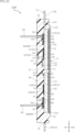
- the third covering layer 732 and the fourth covering layer 733 each have a first layer 751, a second layer 752, and a third layer 753.
- the first layer 751 covers the base layer 731.
- the first layer 751 contains nickel (Ni).
- the second layer 752 covers the first layer 751.
- the second layer 752 contains copper. That is, the second layer 752 includes the metal contained in each of the two support layers 112 and the two conductive layers 12. Therefore, the Vickers hardness of the first layer 751 is greater than the Vickers hardness of the second layer 752.
- the third layer 753 covers the second layer 752.
- the third layer 753 faces either of the two first coating layers 71 and the two second coating layers 72.
- the third layer 753 contains either silver or gold.
- the third layer 753 contains silver.
- the thermal conductivity of the third layer 753 is higher than that of the second layer 752.
- the first bonding layer 74A is located at the interface between one of the two first coating layers 71 and the third layer 753 of the third coating layer 732 facing thereto.
- the second bonding layer 74B is located at the interface between one of the two second covering layers 72 and the opposing third layer 753 of the fourth covering layer 733.
- the degree of diffusion of the second layer 752 into the third layer 753, each of the two first covering layers 71, and each of the two second covering layers is as follows: and the degree of diffusion of the first layer 751 into each of the two second covering layers.
- the third covering layer 732 and the fourth covering layer 733 each have a first layer 751, a second layer 752, and a third layer 753, for example, by sputtering a plurality of layers on each side of the base layer 731 in the first direction z. It can be formed by depositing and stacking metal thin films.
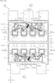
- Each of the plurality of semiconductor elements 21 is mounted on either the first conductive layer 12A or the second conductive layer 12B, as shown in FIGS. 5 and 9.
- the semiconductor element 21 is, for example, a MOSFET (Metal-Oxide-Semiconductor Field-Effect Transistor).
- the semiconductor element 21 may be a switching element such as an IGBT (Insulated Gate Bipolar Transistor) or a diode.
- the semiconductor element 21 is an n-channel type MOSFET with a vertical structure.
- Semiconductor element 21 includes a compound semiconductor substrate.
- the composition of the compound semiconductor substrate includes silicon carbide (SiC).
- the plurality of semiconductor elements 21 include a plurality of first elements 21A and a plurality of second elements 21B.
- the structure of each of the plurality of second elements 21B is the same as the structure of each of the plurality of first elements 21A.
- the plurality of first elements 21A are mounted on the main surface 121 of the first conductive layer 12A.
- the plurality of first elements 21A are arranged along the third direction y.
- the plurality of second elements 21B are mounted on the main surface 121 of the second conductive layer 12B.
- the plurality of second elements 21B are arranged along the third direction y.
- the plurality of semiconductor elements 21 have a first electrode 211, a second electrode 212, a third electrode 213, and a fourth electrode 214.
- the first electrode 211 faces either the first conductive layer 12A or the second conductive layer 12B.
- a current corresponding to the power before being converted by the semiconductor element 21 flows through the first electrode 211 . That is, the first electrode 211 corresponds to the drain electrode of the semiconductor element 21.
- the second electrode 212 is located on the opposite side from the first electrode 211 in the first direction z. A current corresponding to the power converted by the semiconductor element 21 flows through the second electrode 212 . That is, the second electrode 212 corresponds to the source electrode of the semiconductor element 21.
- the third electrode 213 is located on the same side as the second electrode 212 in the first direction z.
- a gate voltage for driving the semiconductor element 21 is applied to the third electrode 213 . That is, the third electrode 213 corresponds to the gate electrode of the semiconductor element 21.
- the area of the third electrode 213 is smaller than the area of the second electrode 212 when viewed in the first direction z.
- the fourth electrode 214 is located on the same side as the second electrode 212 in the first direction z, and next to the third electrode 213 in the third direction y.
- the potential of the fourth electrode 214 is equal to the potential of the second electrode 212.
- the conductive bonding layer 29 is interposed between either the first conductive layer 12A or the second conductive layer 12B and the first electrode 211 of any one of the plurality of semiconductor elements 21. ing.
- the conductive bonding layer 29 is, for example, solder.
- the conductive bonding layer 29 may include a sintered body of metal particles.
- the first electrodes 211 of the plurality of first elements 21A are conductively bonded to the main surface 121 of the first conductive layer 12A via the conductive bonding layer 29. Thereby, the first electrodes 211 of the plurality of first elements 21A are electrically connected to the first conductive layer 12A.
- the first electrodes 211 of the plurality of second elements 21B are conductively bonded to the main surface 121 of the second conductive layer 12B via the conductive bonding layer 29. Thereby, the first electrodes 211 of the plurality of second elements 21B are electrically connected to the second conductive layer 12B.
- the first input terminal 13 is located on the opposite side of the second conductive layer 12B with the first conductive layer 12A in between in the second direction x, and Connected to 12A. Thereby, the first input terminal 13 is electrically connected to the first electrodes 211 of the plurality of first elements 21A via the first conductive layer 12A.
- the first input terminal 13 is a P terminal (positive electrode) to which a DC power supply voltage to be subjected to power conversion is applied.
- the first input terminal 13 extends in the second direction x from the first conductive layer 12A.
- the first input terminal 13 has a covering portion 13A and an exposed portion 13B. As shown in FIG.
- the covering portion 13A is connected to the first conductive layer 12A and covered with the sealing resin 50.
- the covering portion 13A is flush with the main surface 121 of the first conductive layer 12A.
- the exposed portion 13B extends from the covering portion 13A in the second direction x and is exposed from the sealing resin 50.
- the output terminal 14 is located on the opposite side of the first conductive layer 12A with the second conductive layer 12B in between in the second direction x, and is connected to the second conductive layer 12B. linked. Thereby, the output terminal 14 is electrically connected to the first electrodes 211 of the plurality of second elements 21B via the second conductive layer 12B.
- the AC power converted by the semiconductor element 21 is output from the output terminal 14 .
- the output terminal 14 includes two regions separated from each other in the third direction y. Alternatively, the output terminal 14 may have a single configuration that does not include two areas.
- the output terminal 14 has a covered portion 14A and an exposed portion 14B. As shown in FIG.
- the covering portion 14A is connected to the second conductive layer 12B and covered with the sealing resin 50.
- the covering portion 14A is flush with the main surface 121 of the second conductive layer 12B.
- the exposed portion 14B extends from the covering portion 14A in the second direction x and is exposed from the sealing resin 50.
- the second input terminal 15 is located on the same side as the first input terminal 13 with respect to the first conductive layer 12A and the second conductive layer 12B in the second direction x, and It is separated from the first conductive layer 12A and the second conductive layer 12B.
- the second input terminal 15 is electrically connected to the second electrodes 212 of the plurality of second elements 21B.
- the second input terminal 15 is an N terminal (negative electrode) to which a DC power supply voltage to be subjected to power conversion is applied.
- the second input terminal 15 includes two regions separated from each other in the third direction y.
- the first input terminal 13 is located between the two regions in the third direction y.
- the second input terminal 15 has a covering portion 15A and an exposed portion 15B. As shown in FIG. 8, the covering portion 15A is separated from the first conductive layer 12A and covered with the sealing resin 50.
- the exposed portion 15B extends from the covering portion 15A in the second direction x and is exposed from the sealing resin 50.
- the two control wirings 60 include a first signal terminal 161, a second signal terminal 162, a third signal terminal 171, a fourth signal terminal 172, two fifth signal terminals 181, two sixth signal terminals 182, and a plurality of It constitutes a part of the conductive path with the semiconductor element 21.
- the two control wires 60 include a first wire 601 and a second wire 602.
- the first wiring 601 is located between the plurality of first elements 21A, the first input terminal 13, and the second input terminal 15.
- the first wiring 601 is bonded to the main surface 121 of the first conductive layer 12A.
- the first wiring 601 also constitutes a part of the conductive path between the seventh signal terminal 19 and the first conductive layer 12A.
- the second wiring 602 is located between the plurality of second elements 21B and the output terminal 14.
- the second wiring 602 is bonded to the main surface 121 of the second conductive layer 12B.
- the two control wirings 60 have an insulating layer 61, a plurality of wiring layers 62, an intermediate layer 63, and a plurality of sleeves 64.
- the two control wirings 60 are covered with the sealing resin 50 except for a portion of each of the plurality of sleeves 64.
- the insulating layer 61 includes a portion interposed between the plurality of wiring layers 62 and the intermediate layer 63 in the first direction z.
- the insulating layer 61 is made of ceramics, for example.
- the insulating layer 61 may be made of an insulating resin sheet instead of ceramics.
- the plurality of wiring layers 62 are located on one side of the insulating layer 61 in the first direction z.
- the composition of the plurality of wiring layers 62 includes copper.
- the multiple wiring layers 62 include a first wiring layer 621, a second wiring layer 622, two third wiring layers 623, a fourth wiring layer 624, and a fifth wiring layer 625.
- the two third wiring layers 623 are adjacent to each other in the third direction y.
- the intermediate layer 63 is located on the opposite side from the plurality of wiring layers 62 with the insulating layer 61 in between in the first direction z.
- the composition of intermediate layer 63 includes copper.
- the intermediate layer 63 of the first wiring 601 is bonded to the main surface 121 of the first conductive layer 12A by a first bonding layer 68.
- the intermediate layer 63 of the second wiring 602 is bonded to the main surface 121 of the second conductive layer 12B by a first bonding layer 68.
- the first bonding layer 68 is made of a material that may or may not be electrically conductive.
- the first bonding layer 68 is, for example, solder.
- each of the plurality of sleeves 64 is bonded to one of the plurality of wiring layers 62 by a second bonding layer 69.
- the plurality of sleeves 64 are made of a conductive material such as metal.
- Each of the plurality of sleeves 64 has a cylindrical shape extending along the first direction z.
- One end of the plurality of sleeves 64 is electrically conductively bonded to one of the plurality of wiring layers 62.
- an end surface 641 corresponding to the other end of the plurality of sleeves 64 is exposed from the top surface 51 of the sealing resin 50, which will be described later.
- the second bonding layer 69 has conductivity.
- the second bonding layer 69 is, for example, solder.
- one of the two thermistors 22 is electrically connected to the two third wiring layers 623 of the first wiring 601.
- the other thermistor 22 of the two thermistors 22 is conductively bonded to the two third wiring layers 623 of the second wiring 602, as shown in FIG.
- the two thermistors 22 are, for example, NTC (Negative Temperature Coefficient) thermistors.
- the NTC thermistor has a characteristic that its resistance gradually decreases as the temperature rises.
- the two thermistors 22 are used as temperature detection sensors of the semiconductor device A10.
- the first signal terminal 161, second signal terminal 162, third signal terminal 171, fourth signal terminal 172, two fifth signal terminals 181, two sixth signal terminals 182, and seventh signal terminal 19 are shown in FIG. As shown in the figure, it is made up of a metal pin extending in the first direction z. These terminals protrude from a top surface 51 of a sealing resin 50, which will be described later. Furthermore, these terminals are individually press-fitted into the plurality of sleeves 64 of the two control wirings 60. Thereby, each of these terminals is supported by one of the plurality of sleeves 64 and is electrically connected to one of the plurality of wiring layers 62.
- the first signal terminal 161 is press-fitted into a sleeve 64 joined to the first wiring layer 621 of the first wiring 601 among the plurality of sleeves 64 of the two control wirings 60. There is. Thereby, the first signal terminal 161 is supported by the sleeve 64 and is electrically connected to the first wiring layer 621 of the first wiring 601. Further, the first signal terminal 161 is electrically connected to the third electrode 213 of the plurality of first elements 21A. A gate voltage for driving the plurality of first elements 21A is applied to the first signal terminal 161.
- the second signal terminal 162 is press-fitted into a sleeve 64 joined to the first wiring layer 621 of the second wiring 602 among the plurality of sleeves 64 of the two control wirings 60. There is. Thereby, the second signal terminal 162 is supported by the sleeve 64 and electrically connected to the first wiring layer 621 of the second wiring 602. Further, the second signal terminal 162 is electrically connected to the third electrode 213 of the plurality of second elements 21B. A gate voltage for driving the plurality of second elements 21B is applied to the second signal terminal 162.
- the third signal terminal 171 is located next to the first signal terminal 161 in the third direction y. As shown in FIG. 5, the third signal terminal 171 is press-fitted into the sleeve 64 of the plurality of sleeves 64 of the two control wirings 60, which is joined to the second wiring layer 622 of the first wiring 601. Thereby, the third signal terminal 171 is supported by the sleeve 64 and electrically connected to the second wiring layer 622 of the first wiring 601. Furthermore, the third signal terminal 171 is electrically connected to the fourth electrode 214 of the plurality of first elements 21A. A voltage corresponding to the maximum current flowing through the fourth electrode 214 of each of the plurality of first elements 21A is applied to the third signal terminal 171.
- the fourth signal terminal 172 is located next to the second signal terminal 162 in the third direction y. As shown in FIG. 5, the fourth signal terminal 172 is press-fitted into a sleeve 64 joined to the second wiring layer 622 of the second wiring 602, among the plurality of sleeves 64 of the two control wirings 60. Thereby, the fourth signal terminal 172 is supported by the sleeve 64 and is electrically connected to the second wiring layer 622 of the second wiring 602. Further, the fourth signal terminal 172 is electrically connected to the fourth electrode 214 of the plurality of second elements 21B. A voltage corresponding to the maximum current flowing through the fourth electrode 214 of each of the plurality of second elements 21B is applied to the fourth signal terminal 172.
- the two fifth signal terminals 181 are located on the opposite side of the third signal terminal 171 with the first signal terminal 161 in between in the third direction y.
- the two fifth signal terminals 181 are adjacent to each other in the third direction y.
- the two fifth signal terminals 181 are connected to the two sleeves 64 that are joined to the two third wiring layers 623 of the first wiring 601 among the plurality of sleeves 64 of the two control wirings 60. Individually press-fitted.
- the two fifth signal terminals 181 are supported by the two sleeves 64 and electrically connected to the two third wiring layers 623 of the first wiring 601.
- the two fifth signal terminals 181 are electrically connected to one of the two thermistors 22 that is electrically connected to the two third wiring layers 623 of the first wiring 601 .
- the two sixth signal terminals 182 are located on the opposite side of the fourth signal terminal 172 with the second signal terminal 162 in between in the third direction y.
- the two sixth signal terminals 182 are adjacent to each other in the third direction y.
- the two sixth signal terminals 182 are connected to the two sleeves 64 that are joined to the two third wiring layers 623 of the second wiring 602 among the plurality of sleeves 64 of the two control wirings 60. Individually press-fitted.
- the two sixth signal terminals 182 are supported by the two sleeves 64 and electrically connected to the two third wiring layers 623 of the second wiring 602.
- the two sixth signal terminals 182 are electrically connected to one of the two thermistors 22 that is electrically connected to the two third wiring layers 623 of the second wiring 602 .
- the seventh signal terminal 19 is located on the opposite side of the first signal terminal 161 with the third signal terminal 171 interposed therebetween in the third direction y. As shown in FIG. 5, the seventh signal terminal 19 is press-fitted into a sleeve 64 of the plurality of sleeves 64 of the two control wirings 60, which is joined to the fifth wiring layer 625 of the first wiring 601. Thereby, the seventh signal terminal 19 is supported by the sleeve 64 and electrically connected to the fifth wiring layer 625 of the first wiring 601. Further, the seventh signal terminal 19 is electrically connected to the first conductive layer 12A. A voltage corresponding to the DC power input to the first input terminal 13 and the second input terminal 15 is applied to the seventh signal terminal 19 .
- the plurality of first wires 41 are conductively bonded to the third electrodes 213 of the plurality of first elements 21A and the fourth wiring layer 624 of the first wiring 601.
- the plurality of third wires 43 are electrically conductively bonded to the fourth wiring layer 624 of the first wiring 601 and the first wiring layer 621 of the first wiring 601, as shown in FIG. Thereby, the first signal terminal 161 is electrically connected to the third electrode 213 of the plurality of first elements 21A.
- the compositions of the plurality of first wires 41 and the plurality of third wires 43 include gold.
- the compositions of the plurality of first wires 41 and the plurality of third wires 43 may include copper or aluminum.
- the plurality of first wires 41 are electrically connected to the third electrodes 213 of the plurality of second elements 21B and the fourth wiring layer 624 of the second wiring 602.
- the plurality of third wires 43 are electrically connected to the fourth wiring layer 624 of the second wiring 602 and the first wiring layer 621 of the second wiring 602, as shown in FIG.
- the second signal terminal 162 is electrically connected to the third electrodes 213 of the plurality of second elements 21B.
- the plurality of second wires 42 are conductively bonded to the fourth electrodes 214 of the plurality of first elements 21A and the second wiring layer 622 of the first wiring 601.
- the third signal terminal 171 is electrically connected to the fourth electrode 214 of the plurality of first elements 21A.
- the plurality of second wires 42 are electrically connected to the fourth electrodes 214 of the plurality of second elements 21B and the second wiring layer 622 of the second wiring 602, as shown in FIG.
- the fourth signal terminal 172 is electrically connected to the fourth electrodes 214 of the plurality of second elements 21B.
- the composition of the plurality of second wires 42 includes gold.
- the composition of the plurality of second wires 42 may include copper or aluminum.
- the fourth wire 44 is conductively bonded to the fifth wiring layer 625 of the first wiring 601 and the main surface 121 of the first conductive layer 12A. Thereby, the seventh signal terminal 19 is electrically connected to the first conductive layer 12A.
- the composition of the fourth wire 44 includes gold.
- the composition of the fourth wire 44 may include copper or aluminum.
- the first conductive member 31 is electrically bonded to the second electrodes 212 of the plurality of first elements 21A and the main surface 121 of the second conductive layer 12B. Thereby, the second electrodes 212 of the plurality of first elements 21A are electrically connected to the second conductive layer 12B.
- the composition of the first conductive member 31 includes copper.
- the first conductive member 31 is a metal clip. As shown in FIG. 5, the first conductive member 31 includes a main body portion 311, a plurality of first joint portions 312, a plurality of first connection portions 313, a second joint portion 314, and a second connection portion 315.
- the main body part 311 constitutes the main part of the first conductive member 31. As shown in FIG. 5, the main body portion 311 extends in the third direction y. As shown in FIG. 9, the main body portion 311 straddles between the first conductive layer 12A and the second conductive layer 12B.
- the plurality of first bonding parts 312 are individually bonded to the second electrodes 212 of the plurality of first elements 21A.
- Each of the plurality of first joint portions 312 faces one of the second electrodes 212 of the plurality of first elements 21A.
- the plurality of first connecting parts 313 are connected to the main body part 311 and the plurality of first joint parts 312.
- the plurality of first connecting portions 313 are separated from each other in the third direction y.
- the plurality of first connecting portions 313 move away from the main surface 121 of the first conductive layer 12A as they move from the plurality of first joint portions 312 toward the main body portion 311. It is tilted in the direction.
- the second bonding portion 314 is bonded to the main surface 121 of the second conductive layer 12B.
- the second joint portion 314 faces the main surface 121.
- the second joint portion 314 extends in the third direction y.
- the dimension of the second joint portion 314 in the third direction y is equal to the dimension of the main body portion 311 in the third direction y.
- the second connecting portion 315 is connected to the main body portion 311 and the second joint portion 314.
- the second connecting portion 315 is inclined away from the main surface 121 of the second conductive layer 12B as it goes from the second joint portion 314 toward the main body portion 311.
- the dimension of the second connecting portion 315 in the third direction y is equal to the dimension of the main body portion 311 in the third direction y.
- the semiconductor device A10 further includes a first conductive bonding layer 33, as shown in FIGS. 9, 10, and 13.
- the first conductive bonding layer 33 is interposed between the second electrodes 212 of the plurality of first elements 21A and the plurality of first bonding portions 312.
- the first conductive bonding layer 33 conductively bonds the second electrodes 212 of the plurality of first elements 21A and the plurality of first bonding portions 312.
- the first conductive bonding layer 33 is, for example, solder.
- the first conductive bonding layer 33 may include a sintered body of metal particles.
- the semiconductor device A10 further includes a second conductive bonding layer 34, as shown in FIG.
- the second conductive bonding layer 34 is interposed between the main surface 121 of the second conductive layer 12B and the second bonding portion 314.
- the second conductive bonding layer 34 conductively bonds the main surface 121 and the second bonding portion 314 together.
- the second conductive bonding layer 34 is, for example, solder.
- the second conductive bonding layer 34 may include a sintered body of metal particles.
- the second conductive member 32 is electrically connected to the second electrodes 212 of the plurality of second elements 21B and the covering portion 15A of the second input terminal 15, as shown in FIGS. 4 and 11. Thereby, the second electrodes 212 of the plurality of second elements 21B are electrically connected to the second input terminal 15.
- the composition of the second conductive member 32 includes copper.
- the second conductive member 32 is a metal clip. As shown in FIG. 4, the second conductive member 32 includes two main body parts 321, a plurality of third joint parts 322, a plurality of third joint parts 323, two fourth joint parts 324, and two fourth joint parts. 325, a plurality of intermediate portions 326, and a plurality of cross beam portions 327.
- the two main body parts 321 are separated from each other in the third direction y.
- the two main body parts 321 extend in the second direction x.
- the two main bodies 321 are arranged parallel to the main surface 121 of the first conductive layer 12A and the main surface 121 of the second conductive layer 12B.
- the two body parts 321 are further away from the main surface 121 and the main surface 121 than the main body part 311 of the first conductive member 31 is.
- the plurality of intermediate portions 326 are spaced apart from each other in the third direction y, and are located between the two main body portions 321 in the third direction y.
- the plurality of intermediate portions 326 extend in the second direction x.
- the dimension of each of the plurality of intermediate portions 326 in the second direction x is smaller than the dimension of each of the two main body portions 321 in the second direction x.
- the plurality of third joint parts 322 are individually joined to the second electrodes 212 of the plurality of second elements 21B.
- Each of the plurality of third joints 322 faces one of the second electrodes 212 of the plurality of second elements 21B.
- the plurality of third connecting parts 323 are connected to both sides of the plurality of third joint parts 322 in the third direction y. Further, the plurality of third connecting portions 323 are connected to either of the two main body portions 321 and the plurality of intermediate portions 326. As viewed in the second direction x, each of the plurality of third connecting portions 323 increases as it moves from one of the plurality of third joint portions 322 toward one of the two main body portions 321 and the plurality of intermediate portions 326. It is inclined in a direction away from main surface 121 of second conductive layer 12B.
- the two fourth joint parts 324 are joined to the covering part 15A of the second input terminal 15.
- the two fourth joints 324 face the covering portion 15A.
- the two fourth connecting portions 325 are connected to the two main body portions 321 and the two fourth joint portions 324.
- the two fourth connecting parts 325 are inclined in a direction away from the main surface 121 of the first conductive layer 12A from the two fourth joint parts 324 toward the two main body parts 321. There is.
- the plurality of horizontal beams 327 are arranged along the third direction y.
- the plurality of horizontal beam portions 327 include regions that individually overlap the plurality of first joint portions 312 of the first conductive member 31.
- Both sides in the third direction y of the cross beam part 327 located at the center in the third direction y among the plurality of cross beam parts 327 are connected to the plurality of intermediate parts 326 .
- Both sides of the remaining two cross beam portions 327 in the third direction y among the plurality of cross beam portions 327 are connected to one of the two main body portions 321 and one of the plurality of intermediate portions 326.
- the plurality of horizontal beam portions 327 When viewed in the second direction x, the plurality of horizontal beam portions 327 have a convex shape on the side toward which the main surface 121 of the first conductive layer 12A faces in the first direction z.
- the semiconductor device A10 further includes a third conductive bonding layer 35, as shown in FIGS. 9, 11, and 12.
- the third conductive bonding layer 35 is interposed between the second electrodes 212 of the plurality of second elements 21B and the plurality of third bonding parts 322.
- the third conductive bonding layer 35 conductively bonds the second electrodes 212 of the plurality of second elements 21B and the plurality of third bonding parts 322.
- the third conductive bonding layer 35 is, for example, solder.
- the third conductive bonding layer 35 may include a sintered body of metal particles.
- the semiconductor device A10 further includes a fourth conductive bonding layer 36, as shown in FIG.
- the fourth conductive bonding layer 36 is interposed between the covering portion 15A of the second input terminal 15 and the two fourth bonding portions 324.
- the fourth conductive bonding layer 36 conductively bonds the covering portion 15A and the two fourth bonding portions 324 together.
- the fourth conductive bonding layer 36 is, for example, solder.
- the fourth conductive bonding layer 36 may include a sintered body of metal particles.
- the sealing resin 50 includes two support layers 112, two conductive layers 12, a plurality of semiconductor elements 21, a first conductive member 31, and a second conductive member. It covers 32. Furthermore, the sealing resin 50 covers a portion of each of the first input terminal 13, the output terminal 14, and the second input terminal 15.
- the sealing resin 50 has electrical insulation properties.
- the sealing resin 50 is made of a material containing, for example, a black epoxy resin. As shown in FIG. 2 and FIGS. 6 to 9, the sealing resin 50 has a top surface 51, a bottom surface 52, two first side surfaces 53, two second side surfaces 54, and two recesses 55.
- the top surface 51 faces the same side as the main surface 121 of each of the two conductive layers 12 in the first direction z.
- the bottom surface 52 faces opposite to the top surface 51 in the first direction z.
- the heat dissipation layer 113 is exposed to the outside from the bottom surface 52.
- the two first side surfaces 53 are separated from each other in the second direction x.
- the two first side surfaces 53 face the second direction x and extend in the third direction y.
- the two first side surfaces 53 are connected to the top surface 51.
- the exposed portion 13B of the first input terminal 13 and the exposed portion 15B of the second input terminal 15 are exposed from one of the two first side surfaces 53.
- the exposed portion 14B of the output terminal 14 is exposed from the other of the two first side surfaces 53.
- the two second side surfaces 54 are separated from each other in the third direction y.
- the two second side surfaces 54 face oppositely to each other in the third direction y and extend in the second direction x.
- the two second side surfaces 54 are connected to the top surface 51 and the bottom surface 52.
- the two recesses 55 are the first side surface where the exposed portion 13B of the first input terminal 13 and the exposed portion 15B of the second input terminal 15 are exposed among the two first side surfaces 53. 53 toward the second direction x.
- the two recesses 55 extend from the top surface 51 to the bottom surface 52 in the first direction z.
- the two recesses 55 are located on both sides of the first input terminal 13 in the third direction y.
- the semiconductor device A10 includes a support layer 112, a conductive layer 12, a semiconductor element 21 bonded to the conductive layer 12, a first covering layer 71 covering the supporting layer 112, and a second covering layer 72 covering the conductive layer 12. , a bonding layer 73 that bonds the first coating layer 71 and the second coating layer 72.
- the bonding layer 73 includes a base layer 731, a third covering layer 732, and a fourth covering layer 733.
- a solid phase bonding layer 74 is formed between the first coating layer 71 and the third coating layer 732 and between the second coating layer 72 and the fourth coating layer 733, respectively.
- the Vickers hardness of the base layer 731 is smaller than the Vickers hardness of each of the support layer 112 and the conductive layer 12.
- the deformation performance of the base layer 731 is higher than the deformation performance of each of the support layer 112 and the conductive layer 12. Since it is large, the contact area of the bonding layer 73 with each of the first coating layer 71 and the second coating layer 72, that is, the bonding area of the solid phase bonding layer 74 becomes larger. This makes the metal bond in the solid phase bonding layer 74 stronger.
- each of the third covering layer 732 and the fourth covering layer 733 of the bonding layer 73 includes a first layer 751, a second layer 752, and a third layer 753.
- the degree of diffusion of the second layer 752 into each of the third layer 753, first covering layer 71, and second covering layer 72 is determined by the degree of diffusion of the second layer 752 into each of the third layer 753, first covering layer 71, and second covering layer This is greater than the degree of diffusion in one layer 751.
- the solid phase bonding layer 74 is formed at each of the interface between the first coating layer 71 and the third coating layer 732 and the interface between the second coating layer 72 and the fourth coating layer 733.
- the first layer 751 functions as a barrier layer that restricts the diffusion of the second layer 752, the diffusion of the second layer 752 into each of the third layer 753, the first covering layer 71, and the second covering layer 72 is prevented. is further promoted, so that the metal bond in the solid phase bonding layer 74 becomes even stronger. Therefore, according to the above configuration, in the semiconductor device A10, the bonding state between the support layer 112 and the conductive layer 12 becomes stronger, so that it is possible to improve the heat dissipation performance of the semiconductor device A10.
- Each of the first coating layer 71, the second coating layer 72, the third layer 753 of the third coating layer 732, and the third layer 753 of the fourth coating layer 733 preferably contains either silver or gold. . Silver and gold are each more susceptible to plastic flow than copper. Therefore, by adopting this configuration, the formation of the solid phase bonding layer 74 is more easily promoted.
- the Vickers hardness of the first layer 751 is larger than the Vickers hardness of the second layer 752.
- the thickness of the conductive layer 12 is greater than the thickness of the support layer 112.
- the semiconductor device A10 further includes an insulating layer 111 located on the opposite side of the conductive layer 12 with respect to the support layer 112. Support layer 112 is bonded to insulating layer 111 . With this configuration, the heat dissipation layer 113 located on the opposite side of the support layer 112 with respect to the insulating layer 111 can be bonded to the insulating layer 111. Thereby, the heat dissipation performance of the semiconductor device A10 can be further improved while ensuring electrical insulation of the heat dissipation layer 113 with respect to the conductive layer 12.
- the conductive layer 12 When viewed in the first direction z, the conductive layer 12 is surrounded by the peripheral edge 112A of the support layer 112.
- the conductive layer 12 When viewed in the first direction z, the conductive layer 12 is surrounded by the peripheral edge 112A of the support layer 112.
- the thickness of the heat dissipation layer 113 is greater than the thickness of the support layer 112.
- FIG. 15 Based on FIG. 15, a semiconductor device A20 according to a second embodiment of the present disclosure will be described.
- elements that are the same as or similar to those of the semiconductor device A10 described above are given the same reference numerals, and redundant explanation will be omitted.
- the cross-sectional position in FIG. 15 is the same as the cross-sectional position in FIG. 14 showing the semiconductor device A10.
- the configurations of the two first coating layers 71 and the two second coating layers 72 are different from the configuration of the semiconductor device A10.
- each of the two first covering layers 71 has a fourth layer 754, a fifth layer 755, and a sixth layer 756.
- Fourth layer 754 covers support layer 112 .
- Fourth layer 754 contains nickel. Therefore, the metal contained in the fourth layer 754 is the same as the metal contained in the first layer 751 of the third coating layer 732 of either of the two bonding layers 73.
- the fifth layer 755 covers the fourth layer 754.
- the fifth layer 755 contains copper. Therefore, the metal contained in the fifth layer 755 is the same as the metal contained in the second layer 752 of the third coating layer 732.
- a sixth layer 756 covers the fifth layer 755.
- the sixth layer 756 contains either silver or gold.
- the sixth layer 756 contains silver. Therefore, the degree of diffusion of the fifth layer 755 into the sixth layer 756 is greater than the degree of diffusion of the fourth layer 754 into the sixth layer 756.
- the first bonding layer 74A of the solid phase bonding layer 74 is located at the interface between the sixth layer 756 and the third layer 753 of the third coating layer 732.
- the first covering layer 71 having the fourth layer 754, the fifth layer 755, and the sixth layer 756 can be formed, for example, by forming and stacking a plurality of metal thin films by a sputtering method.
- each of the two second covering layers 72 has a seventh layer 757, an eighth layer 758, and a ninth layer 759.
- the seventh layer 757 covers the back surface 122 of either of the two conductive layers 12.
- the seventh layer 757 contains nickel. Therefore, the metal contained in the seventh layer 757 is the same as the metal contained in the first layer 751 of the fourth coating layer 733 of either of the two bonding layers 73.
- the eighth layer 758 covers the seventh layer 757.
- the eighth layer 758 contains copper. Therefore, the metal contained in the eighth layer 758 is the same as the metal contained in the second layer 752 of the fourth coating layer 733.
- the ninth layer 759 covers the eighth layer 758.
- the ninth layer 759 faces the third layer 753 of the fourth covering layer 733.
- the ninth layer 759 contains either silver or gold.
- the ninth layer 759 contains silver. Therefore, the degree of diffusion of the eighth layer 758 into the ninth layer 759 is greater than the degree of diffusion of the seventh layer 757 into the ninth layer 759.
- the second bonding layer 74B of the solid phase bonding layer 74 is located at the interface between the ninth layer 759 and the third layer 753 of the fourth coating layer 733.
- the second covering layer 72 having the seventh layer 757, the eighth layer 758, and the ninth layer 759 can be formed, for example, by forming and stacking a plurality of metal thin films using a sputtering method.
- the semiconductor device A20 includes a support layer 112, a conductive layer 12, a semiconductor element 21 bonded to the conductive layer 12, a first covering layer 71 covering the supporting layer 112, and a second covering layer 72 covering the conductive layer 12. , a bonding layer 73 that bonds the first coating layer 71 and the second coating layer 72.
- the bonding layer 73 includes a base layer 731, a third covering layer 732, and a fourth covering layer 733.
- a solid phase bonding layer 74 is formed between the first coating layer 71 and the third coating layer 732 and between the second coating layer 72 and the fourth coating layer 733, respectively.
- the Vickers hardness of the base layer 731 is smaller than the Vickers hardness of each of the support layer 112 and the conductive layer 12.
- each of the third covering layer 732 and the fourth covering layer 733 of the bonding layer 73 includes a first layer 751, a second layer 752, and a third layer 753.
- the degree of diffusion of the second layer 752 into each of the third layer 753, the first covering layer 71 and the second covering layer 72 is This is greater than the degree of diffusion in one layer 751. Therefore, according to the above configuration, also in the semiconductor device A20, the bonding state between the support layer 112 and the conductive layer 12 becomes stronger, so that it is possible to improve the heat dissipation performance of the semiconductor device A20. Further, the semiconductor device A20 has the same configuration as the semiconductor device A10, so that the same effects as the semiconductor device A10 can be achieved.
- the first covering layer 71 includes a fourth layer 754, a fifth layer 755, and a sixth layer 756.
- the metal contained in the fourth layer 754 is the same as the metal contained in the first layer 751 of the third coating layer 732 of the bonding layer 73.
- the metal contained in the fifth layer 755 is the same as the metal contained in the second layer 752 of the third coating layer 732.
- the degree of diffusion of the fifth layer 755 into the sixth layer 756 is greater than the degree of diffusion of the fourth layer 754 into the sixth layer 756.
- the second covering layer 72 includes a seventh layer 757, an eighth layer 758, and a ninth layer 759.
- the metal contained in the seventh layer 757 is the same as the metal contained in the first layer 751 of the fourth coating layer 733 of the bonding layer 73.
- the metal contained in the eighth layer 758 is the same as the metal contained in the second layer 752 of the fourth coating layer 733.
- the degree of diffusion of the eighth layer 758 into the ninth layer 759 is greater than the degree of diffusion of the seventh layer 757 into the ninth layer 759.
- FIGS. 16 to 19 A semiconductor device A30 according to a third embodiment of the present disclosure will be described based on FIGS. 16 to 19.
- elements that are the same as or similar to those of the semiconductor device A10 described above are given the same reference numerals, and redundant explanation will be omitted.
- FIG. 16 for convenience of understanding, the light passes through the first conductive member 31, and illustration of the second conductive member 32 and the sealing resin 50 is omitted.
- the transparent first conductive member 31 is shown by an imaginary line.
- the configurations of the two conductive layers 12 are different from the configuration of the semiconductor device A10.
- the area of the main surface 121 is larger than the area of the back surface 122.
- the back surface 122 of each of the two conductive layers 12 is individually surrounded by the periphery 112A of each of the two support layers 112.
- the main surface 121 of one of the two conductive layers 12 protrudes outward beyond the periphery 112A of one of the two support layers 112 to which the conductive layer 12 is to be bonded.
- the two conductive layers 12 are surrounded by the periphery 111A of the insulating layer 111 when viewed in the first direction z.
- the semiconductor device A30 includes a support layer 112, a conductive layer 12, a semiconductor element 21 bonded to the conductive layer 12, a first covering layer 71 covering the supporting layer 112, and a second covering layer 72 covering the conductive layer 12. , a bonding layer 73 that bonds the first coating layer 71 and the second coating layer 72.
- the bonding layer 73 includes a base layer 731, a third covering layer 732, and a fourth covering layer 733.
- a solid phase bonding layer 74 is formed between the first coating layer 71 and the third coating layer 732 and between the second coating layer 72 and the fourth coating layer 733, respectively.
- the Vickers hardness of the base layer 731 is smaller than the Vickers hardness of each of the support layer 112 and the conductive layer 12.
- each of the third covering layer 732 and the fourth covering layer 733 of the bonding layer 73 includes a first layer 751, a second layer 752, and a third layer 753.
- the degree of diffusion of the second layer 752 into each of the third layer 753, the first covering layer 71 and the second covering layer 72 is This is greater than the degree of diffusion in one layer 751. Therefore, according to the above configuration, also in the semiconductor device A30, the bonding state between the support layer 112 and the conductive layer 12 becomes stronger, so that it is possible to improve the heat dissipation performance of the semiconductor device A30.
- the semiconductor device A30 has the same configuration as the semiconductor device A10, so that it can achieve the same effects as the semiconductor device A10.
- Conductive layer 12 has a main surface 121 facing semiconductor element 21 .
- the area of the main surface 121 is larger than the area of the back surface 122 of the conductive layer 12.
- FIGS. 20 to 23 A semiconductor device A40 according to a fourth embodiment of the present disclosure will be described based on FIGS. 20 to 23.
- elements that are the same as or similar to those of the semiconductor device A10 described above are given the same reference numerals, and redundant explanation will be omitted.
- FIG. 20 for convenience of understanding, the light passes through the first conductive member 31, and illustration of the second conductive member 32 and the sealing resin 50 is omitted.
- the transparent first conductive member 31 is shown by an imaginary line.
- the configurations of the two conductive layers 12 are different from the configuration of the semiconductor device A10.
- each of the two conductive layers 12 when viewed in the first direction z, the main surface 121 and the back surface 122 of each of the two conductive layers 12 are the peripheries of the two support layers 112 to which the conductive layers 12 are to be bonded. It protrudes outward from 112A.
- the area of the back surface 122 is equal to the area of the main surface 121.
- the two conductive layers 12 are surrounded by the periphery 111A of the insulating layer 111 when viewed in the first direction z.
- the semiconductor device A40 includes a support layer 112, a conductive layer 12, a semiconductor element 21 bonded to the conductive layer 12, a first covering layer 71 covering the supporting layer 112, and a second covering layer 72 covering the conductive layer 12. , a bonding layer 73 that bonds the first coating layer 71 and the second coating layer 72.
- the bonding layer 73 includes a base layer 731, a third covering layer 732, and a fourth covering layer 733.
- a solid phase bonding layer 74 is formed between the first coating layer 71 and the third coating layer 732 and between the second coating layer 72 and the fourth coating layer 733, respectively.
- the Vickers hardness of the base layer 731 is smaller than the Vickers hardness of each of the support layer 112 and the conductive layer 12.
- each of the third covering layer 732 and the fourth covering layer 733 of the bonding layer 73 includes a first layer 751, a second layer 752, and a third layer 753.
- the degree of diffusion of the second layer 752 into each of the third layer 753, the first covering layer 71 and the second covering layer 72 is This is greater than the degree of diffusion in one layer 751. Therefore, according to the above configuration, also in the semiconductor device A40, the bonding state between the support layer 112 and the conductive layer 12 becomes stronger, so that it is possible to improve the heat dissipation performance of the semiconductor device A40.
- the semiconductor device A40 has the same configuration as the semiconductor device A10, so that it can achieve the same effects as the semiconductor device A10.
- the present disclosure includes the embodiments described in the appendix below. Additional note 1. a support layer; a conductive layer bonded to the support layer; a semiconductor element located on the opposite side of the support layer with respect to the conductive layer and bonded to the conductive layer; a first coating layer located between the support layer and the conductive layer and covering the support layer; a second coating layer located between the first coating layer and the conductive layer and covering the conductive layer; a bonding layer bonding the first coating layer and the second coating layer,
- the bonding layer includes a base layer, a third coating layer located between the base layer and the first coating layer, and a fourth coating layer located between the base layer and the second coating layer.
- a solid phase bonding layer is formed between each of the first coating layer and the third coating layer and between the second coating layer and the fourth coating layer,
- the Vickers hardness of the base layer is smaller than the Vickers hardness of each of the support layer and the conductive layer
- Each of the third coating layer and the fourth coating layer includes a first layer that covers the base layer, a second layer that covers the first layer, and a third layer that covers the second layer,
- the degree of diffusion of the second layer into each of the third layer, the first coating layer, and the second coating layer is determined by the degree of diffusion of the second layer into each of the third layer, the first coating layer, and the second coating layer.
- a semiconductor device in which the degree of diffusion is greater than that of the first layer. Appendix 2.
- the semiconductor device according to supplementary note 1, wherein the second layer includes a metal contained in each of the support layer and the conductive layer.
- Appendix 3. The semiconductor device according to appendix 2, wherein each of the support layer, the conductive layer, and the second layer contains copper.
- Appendix 4. The semiconductor device according to appendix 2 or 3, wherein each of the first coating layer, the second coating layer, and the third layer contains either silver or gold.
- Appendix 5. 5.
- the semiconductor device according to any one of appendices 2 to 4, wherein the base layer contains aluminum.
- Appendix 6. 6. The semiconductor device according to any one of appendices 2 to 5, wherein the first layer has a Vickers hardness greater than the second layer.
- Appendix 7. The semiconductor device according to appendix 6, wherein the first layer contains nickel.
- the first coating layer has a fourth layer that covers the support layer, a fifth layer that covers the fourth layer, and a sixth layer that covers the fifth layer,
- the metal contained in the fourth layer is the same as the metal contained in the first layer
- the metal contained in the fifth layer is the same as the metal contained in the second layer, 8.
- Appendix 9. further comprising an insulating layer located on the opposite side of the conductive layer with respect to the support layer, The semiconductor device according to appendix 6, wherein the support layer is bonded to the insulating layer.
- the semiconductor element has a first electrode facing the conductive layer, The semiconductor device according to appendix 9, wherein the first electrode is conductively bonded to the conductive layer. Appendix 11. The semiconductor device according to appendix 10, wherein the conductive layer has a thickness greater than the support layer. Appendix 12. The semiconductor device according to appendix 11, wherein the conductive layer is surrounded by a periphery of the support layer in plan view. Appendix 13. The conductive layer has a back surface covered with the second coating layer, The semiconductor device according to appendix 11, wherein the back surface is surrounded by a periphery of the support layer in plan view. Appendix 14.
- the conductive layer has a main surface facing the first electrode,
- Appendix 15. further comprising a heat dissipation layer located on the opposite side of the support layer with respect to the insulating layer, 15.
- Appendix 16 The semiconductor device according to appendix 15, wherein the thickness of the heat dissipation layer is greater than the thickness of the support layer.
- Appendix 17. further comprising a sealing resin that covers the support layer, the conductive layer, and the semiconductor element, The semiconductor device according to appendix 15 or 16, wherein the heat dissipation layer is exposed to the outside from the sealing resin.
Landscapes
- Cooling Or The Like Of Semiconductors Or Solid State Devices (AREA)
- Chemical & Material Sciences (AREA)
- Engineering & Computer Science (AREA)
- Ceramic Engineering (AREA)
Priority Applications (3)
| Application Number | Priority Date | Filing Date | Title |
|---|---|---|---|
| JP2024536872A JPWO2024024371A1 (https=) | 2022-07-27 | 2023-06-27 | |
| CN202380055570.8A CN119585864A (zh) | 2022-07-27 | 2023-06-27 | 半导体装置 |
| US19/027,589 US20250157913A1 (en) | 2022-07-27 | 2025-01-17 | Semiconductor device |
Applications Claiming Priority (2)
| Application Number | Priority Date | Filing Date | Title |
|---|---|---|---|
| JP2022119652 | 2022-07-27 | ||
| JP2022-119652 | 2022-07-27 |
Related Child Applications (1)
| Application Number | Title | Priority Date | Filing Date |
|---|---|---|---|
| US19/027,589 Continuation US20250157913A1 (en) | 2022-07-27 | 2025-01-17 | Semiconductor device |
Publications (1)
| Publication Number | Publication Date |
|---|---|
| WO2024024371A1 true WO2024024371A1 (ja) | 2024-02-01 |
Family
ID=89706044
Family Applications (1)
| Application Number | Title | Priority Date | Filing Date |
|---|---|---|---|
| PCT/JP2023/023816 Ceased WO2024024371A1 (ja) | 2022-07-27 | 2023-06-27 | 半導体装置 |
Country Status (4)
| Country | Link |
|---|---|
| US (1) | US20250157913A1 (https=) |
| JP (1) | JPWO2024024371A1 (https=) |
| CN (1) | CN119585864A (https=) |
| WO (1) | WO2024024371A1 (https=) |
Citations (4)
| Publication number | Priority date | Publication date | Assignee | Title |
|---|---|---|---|---|
| JP2005044931A (ja) * | 2003-07-25 | 2005-02-17 | Shinko Electric Ind Co Ltd | 半導体搭載用基板製造方法、半導体パッケージ製造方法、半導体搭載用基板及び半導体パッケージ |
| JP2016042528A (ja) * | 2014-08-18 | 2016-03-31 | 三菱マテリアル株式会社 | 接合体、パワーモジュール用基板、ヒートシンク付パワーモジュール用基板、接合体の製造方法、パワーモジュール用基板の製造方法、及び、ヒートシンク付パワーモジュール用基板の製造方法 |
| WO2018181417A1 (ja) * | 2017-03-31 | 2018-10-04 | ローム株式会社 | パワーモジュールおよびその製造方法 |
| WO2020091008A1 (ja) * | 2018-10-31 | 2020-05-07 | 三菱マテリアル株式会社 | 金属層付き炭素質部材、及び、熱伝導板 |
-
2023
- 2023-06-27 WO PCT/JP2023/023816 patent/WO2024024371A1/ja not_active Ceased
- 2023-06-27 CN CN202380055570.8A patent/CN119585864A/zh active Pending
- 2023-06-27 JP JP2024536872A patent/JPWO2024024371A1/ja active Pending
-
2025
- 2025-01-17 US US19/027,589 patent/US20250157913A1/en active Pending
Patent Citations (4)
| Publication number | Priority date | Publication date | Assignee | Title |
|---|---|---|---|---|
| JP2005044931A (ja) * | 2003-07-25 | 2005-02-17 | Shinko Electric Ind Co Ltd | 半導体搭載用基板製造方法、半導体パッケージ製造方法、半導体搭載用基板及び半導体パッケージ |
| JP2016042528A (ja) * | 2014-08-18 | 2016-03-31 | 三菱マテリアル株式会社 | 接合体、パワーモジュール用基板、ヒートシンク付パワーモジュール用基板、接合体の製造方法、パワーモジュール用基板の製造方法、及び、ヒートシンク付パワーモジュール用基板の製造方法 |
| WO2018181417A1 (ja) * | 2017-03-31 | 2018-10-04 | ローム株式会社 | パワーモジュールおよびその製造方法 |
| WO2020091008A1 (ja) * | 2018-10-31 | 2020-05-07 | 三菱マテリアル株式会社 | 金属層付き炭素質部材、及び、熱伝導板 |
Also Published As
| Publication number | Publication date |
|---|---|
| US20250157913A1 (en) | 2025-05-15 |
| JPWO2024024371A1 (https=) | 2024-02-01 |
| CN119585864A (zh) | 2025-03-07 |
Similar Documents
| Publication | Publication Date | Title |
|---|---|---|
| WO2012165045A1 (ja) | 半導体装置及び配線基板 | |
| WO2023214500A1 (ja) | 半導体装置 | |
| US20250239506A1 (en) | Semiconductor module | |
| WO2023162722A1 (ja) | 半導体装置および半導体モジュール | |
| WO2023112662A1 (ja) | 半導体モジュールおよび半導体装置 | |
| JP7495225B2 (ja) | 半導体装置 | |
| JP2023088628A (ja) | 半導体装置 | |
| WO2025142335A1 (ja) | 半導体装置 | |
| WO2024024371A1 (ja) | 半導体装置 | |
| WO2024018790A1 (ja) | 半導体装置 | |
| WO2023149257A1 (ja) | 半導体装置 | |
| WO2025173493A1 (ja) | 半導体装置、および半導体装置アッセンブリ | |
| WO2024090193A1 (ja) | 半導体装置 | |
| WO2020144907A1 (ja) | 半導体装置 | |
| WO2024085003A1 (ja) | 半導体装置の冷却構造体 | |
| WO2022259825A1 (ja) | 半導体装置 | |
| WO2024048187A1 (ja) | 半導体装置、および、半導体装置の製造方法 | |
| WO2023032667A1 (ja) | 半導体装置、および半導体装置の取付け構造 | |
| WO2024106219A1 (ja) | 半導体装置 | |
| WO2024018851A1 (ja) | 半導体装置 | |
| WO2023189480A1 (ja) | 半導体素子および半導体装置 | |
| WO2022264833A1 (ja) | 半導体装置 | |
| WO2026053967A1 (ja) | 半導体モジュール | |
| WO2024029385A1 (ja) | 半導体装置 | |
| WO2022259809A1 (ja) | 半導体装置 |
Legal Events
| Date | Code | Title | Description |
|---|---|---|---|
| 121 | Ep: the epo has been informed by wipo that ep was designated in this application |
Ref document number: 23846105 Country of ref document: EP Kind code of ref document: A1 |
|
| WWE | Wipo information: entry into national phase |
Ref document number: 2024536872 Country of ref document: JP |
|
| WWE | Wipo information: entry into national phase |
Ref document number: 202380055570.8 Country of ref document: CN |
|
| NENP | Non-entry into the national phase |
Ref country code: DE |
|
| WWP | Wipo information: published in national office |
Ref document number: 202380055570.8 Country of ref document: CN |
|
| 122 | Ep: pct application non-entry in european phase |
Ref document number: 23846105 Country of ref document: EP Kind code of ref document: A1 |