WO2023223426A1 - 電力用半導体素子の駆動回路および駆動方法ならびにパワーモジュール - Google Patents
電力用半導体素子の駆動回路および駆動方法ならびにパワーモジュール Download PDFInfo
- Publication number
- WO2023223426A1 WO2023223426A1 PCT/JP2022/020535 JP2022020535W WO2023223426A1 WO 2023223426 A1 WO2023223426 A1 WO 2023223426A1 JP 2022020535 W JP2022020535 W JP 2022020535W WO 2023223426 A1 WO2023223426 A1 WO 2023223426A1
- Authority
- WO
- WIPO (PCT)
- Prior art keywords
- voltage
- circuit
- power semiconductor
- gate
- slope
- Prior art date
- Legal status (The legal status is an assumption and is not a legal conclusion. Google has not performed a legal analysis and makes no representation as to the accuracy of the status listed.)
- Ceased
Links
Images













Classifications
-
- H—ELECTRICITY
- H03—ELECTRONIC CIRCUITRY
- H03K—PULSE TECHNIQUE
- H03K17/00—Electronic switching or gating, i.e. not by contact-making and –breaking
- H03K17/16—Modifications for eliminating interference voltages or currents
- H03K17/161—Modifications for eliminating interference voltages or currents in field-effect transistor switches
- H03K17/162—Modifications for eliminating interference voltages or currents in field-effect transistor switches without feedback from the output circuit to the control circuit
-
- H—ELECTRICITY
- H03—ELECTRONIC CIRCUITRY
- H03K—PULSE TECHNIQUE
- H03K17/00—Electronic switching or gating, i.e. not by contact-making and –breaking
- H03K17/04—Modifications for accelerating switching
- H03K17/041—Modifications for accelerating switching without feedback from the output circuit to the control circuit
- H03K17/0412—Modifications for accelerating switching without feedback from the output circuit to the control circuit by measures taken in the control circuit
- H03K17/04123—Modifications for accelerating switching without feedback from the output circuit to the control circuit by measures taken in the control circuit in field-effect transistor switches
-
- H—ELECTRICITY
- H03—ELECTRONIC CIRCUITRY
- H03K—PULSE TECHNIQUE
- H03K17/00—Electronic switching or gating, i.e. not by contact-making and –breaking
- H03K17/28—Modifications for introducing a time delay before switching
- H03K17/284—Modifications for introducing a time delay before switching in field effect transistor switches
Definitions
- the present disclosure relates to a drive circuit and a drive method for a power semiconductor element, and a power module.
- Power semiconductor devices that control large amounts of power are used, for example, in power supply circuits that generate alternating current with different frequencies from direct current and alternating current, and in power converters having power supply circuits.
- a power semiconductor element is used in a power conversion device such as an inverter, it is important to suppress power consumption from the viewpoint of energy saving and greenhouse gas reduction.
- Patent Document 1 discloses a method of reducing energy consumed by a power semiconductor element by controlling switching of the power semiconductor element.
- this document describes "a method for driving a power transistor switch, comprising the steps of receiving a drive input signal, converting the drive input signal to a conversion drive input signal, and using the conversion drive input signal to control the switch.
- the conversion drive input signal has three regions in time, each having a slope, the first region being the Miller Plateau of the switch.
- the second region is the time when there is a second slope consisting of a smaller slope compared to the first slope
- the third region is the time when there is a third slope larger than the second slope.
- control electrode voltage quickly reaches the Miller plateau voltage, then slowly reaches the threshold voltage of the switch, and then, when the switch is almost fully turned on, the control electrode voltage
- the switch delay time is maintained substantially constant by adjusting the transistor control electrode precharge voltage.
- Patent Document 1 According to the control method for a power semiconductor device disclosed in the above-mentioned Japanese translations of PCT publication No. 2008-519529 (Patent Document 1), EMI (electromagnetic interference) is reduced by reducing the current change rate (dI/dt) during switching. can be lowered. However, if the current change rate is controlled to be small when the current I flowing through the power semiconductor element is large, there is a problem in that switching time increases and switching loss increases. The above patent documents do not consider this point.
- the present disclosure has been made in consideration of the above problems, and one of the purposes is to provide a power semiconductor device that can suppress switching loss even when a relatively large current flows through the power semiconductor device.
- An object of the present invention is to provide a driving circuit for an element.
- a drive circuit for a power semiconductor device includes a first gate voltage control circuit and a second gate voltage control circuit.
- the first gate voltage control circuit controls the power semiconductor device in different manners in the order of a first time domain, a second time domain, and a third time domain in response to a turn-on command of the power semiconductor device.
- the gate voltage is made to reach the mirror voltage.
- the gate voltage reaches the mirror voltage in the second time domain or in the third time domain, depending on the magnitude of the main current flowing through the power semiconductor element.
- the second gate voltage control circuit controls a gate voltage equal to or higher than the mirror voltage.
- the drive circuit operates in different manners in the first time domain, the second time domain, and the third time domain in response to the turn-on command of the power semiconductor device.
- the gate voltage is made to reach the mirror voltage. Therefore, switching loss can be suppressed even when the current flowing through the power semiconductor element is relatively large.
- FIG. 1 is a block diagram showing the configuration of a drive circuit for a power semiconductor device according to a first embodiment
- FIG. FIG. 3 is a diagram showing an example of the configuration of a voltage limiting circuit.
- FIG. 3 is a diagram illustrating an example of the configuration of a first variable voltage generation circuit.
- FIG. 3 is a diagram illustrating an example of the configuration of a first variable voltage generation circuit.
- FIG. 3 is a diagram illustrating an example of the configuration of a second variable voltage generation circuit.
- FIG. 3 is a diagram illustrating an example of the configuration of a second variable voltage generation circuit.
- FIG. 3 is a diagram showing an example of the configuration of a comparison circuit.
- FIG. 3 is a diagram showing an example of the configuration of an adder circuit.
- FIG. 3 is a diagram showing an example of the configuration of an adder circuit.
- FIG. 3 is a diagram showing an example of the configuration of a buffer circuit.
- FIG. 3 is a diagram showing an example of the configuration of a buffer circuit.
- FIG. 3 is a diagram showing an example of the configuration of a buffer circuit.
- FIG. 1 is a diagram showing an example of the configuration of a power semiconductor element.
- FIG. 2 is a timing chart for explaining a first operation example of the power semiconductor element drive circuit according to the first embodiment.
- 7 is a timing chart for explaining a second operation example of the power semiconductor device drive circuit according to the first embodiment.
- FIG. 5 is a flowchart showing a control procedure when the power semiconductor device is turned on by the drive circuit of the first embodiment.
- FIG. 3 is a diagram showing an example of a mounting aspect of the drive circuit according to the first embodiment.
- FIG. 17 is a diagram showing a modification of the implementation mode of FIG. 16.
- FIG. 7 is a diagram illustrating another example of the implementation mode of the drive circuit of the first embodiment.
- FIG. 19 is a diagram showing a modification of the implementation mode of FIG. 18.
- FIG. 7 is a diagram showing the configuration of a drive circuit for a power semiconductor element according to a second embodiment.
- FIG. 2 is a diagram showing an example of the configuration of a mirror voltage detection circuit.
- FIG. 2 is a diagram showing an example of the configuration of a differentiating circuit.
- FIG. 2 is a diagram showing an example of the configuration of a differentiating circuit.
- FIG. 2 is a diagram showing an example of the configuration of a binarization circuit.
- FIG. 3 is a diagram showing an example of the configuration of an edge detection circuit.
- FIG. 2 is a diagram showing an example of the configuration of a flip-flop circuit. This is an example of a configuration of an inverting circuit.
- FIG. 7 is a timing diagram for explaining an example of the operation of the power semiconductor drive circuit according to the second embodiment. 7 is a flowchart showing a control procedure when the power semiconductor device is turned on by the drive circuit according to the second embodiment.
- FIG. 1 is a block diagram showing the configuration of a power semiconductor device drive circuit 1000 according to the first embodiment.
- Drive circuit 1000 generates gate voltage Vg for controlling switching of power semiconductor element 8 according to a control signal input to control input terminal 7 . More specifically, the drive circuit 1000 sequentially changes the voltage change of the gate voltage Vg during the turn-on operation of the power semiconductor element 8 from the first time domain (RG1 in FIGS. 13 and 14) to the fourth time domain (RG1 in FIGS. 13 and 14). Control is performed in four time domains up to RG4) in FIGS. 13 and 14.
- the first to fourth time regions are also simply referred to as first to fourth regions.
- the drive circuit 1000 includes a voltage limiting circuit 1, a first variable voltage generation circuit 2, a second variable voltage generation circuit 3, a comparison circuit 4, an addition circuit 5, and a buffer circuit. 6.
- the voltage limiting circuit 1, the first variable voltage generation circuit 2, the second variable voltage generation circuit 3, the addition circuit 5, and the buffer circuit 6 are collectively referred to as a first gate voltage control circuit 10.
- the first gate voltage control circuit 10 controls the power semiconductor element 8 in different ways in the order of a first time domain RG1, a second time domain RG2, and a third time domain RG3 in response to the turn-on command.
- the gate voltage Vg is made to reach the mirror voltage Vm.
- the gate voltage Vg reaches the mirror voltage Vm in the second region RG2 or the third region RG3.
- Comparison circuit 4 as a second gate voltage control circuit controls gate voltage Vg after the mirror period. The functions of each circuit are briefly described below.
- the voltage limiting circuit 1 controls the voltage change of the gate voltage Vg in the first region RG1. Specifically, the voltage limiting circuit 1 outputs a limiting voltage VL (also referred to as a first voltage) in response to a turn-on command, thereby increasing the voltage up to the limiting voltage VL at a first slope (SL1 in FIGS. 13 and 14). Rapidly increase gate voltage Vg. That is, the voltage limiting circuit 1 limits the gate voltage Vg to the limit voltage VL when the power semiconductor element 8 rises.
- the limit voltage VL corresponds to the threshold voltage Vth of the power semiconductor element 8 and has a value approximately equal to the threshold voltage Vth.
- the first variable voltage generation circuit 2 controls the voltage change of the gate voltage Vg in the second region RG2. Specifically, the first variable voltage generation circuit 2 generates the first variable voltage V1 that increases at a second slope (SL2 in FIGS. 13 and 14) that is gentler than the first slope SL1. The first variable voltage generation circuit 2 supplies the generated first variable voltage V1 to the gate of the power semiconductor element 8 via the buffer circuit 6, thereby changing the gate voltage Vg from the limit voltage VL to a second slope. Increase at SL2.
- the second variable voltage generation circuit 3 controls the voltage change of the gate voltage Vg in the third region RG3. Specifically, the second variable voltage generation circuit 3 generates a second variable voltage V2 that changes more steeply than the first variable voltage V1 output from the first variable voltage generation circuit 2. As a result, if the gate voltage Vg has not reached the mirror voltage when the first period (from time t0 to t3 in FIG. 13, from time t0 to t2 in FIG. 14) has elapsed after receiving the turn-on command, At a third slope SL3 that is gentler than the first slope SL1 but steeper than the second slope SL2, the gate voltage Vg increases to the mirror voltage.
- the comparison circuit 4 controls the voltage change of the gate voltage Vg in the fourth region RG4. Specifically, the comparator circuit 4 calculates a fourth slope steeper than the third slope SL3 from the time when a second period (from time t0 to t4 in FIGS. 13 and 14) has elapsed after receiving the turn-on command. The gate voltage Vg is increased from the mirror voltage by the slope SL4. Eventually, the gate voltage Vg reaches the power supply voltage supplied to the drive circuit 1000.
- the adder circuit 5 outputs a voltage obtained by adding the first variable voltage V1 to the limited voltage VL until the above-mentioned first period has elapsed after receiving the turn-on command.
- the adder circuit 5 adjusts the output current of the voltage limiting circuit 1, the output current of the first variable voltage generation circuit 2, and the output current of the second variable voltage generation circuit from the time when the above-mentioned first period has elapsed after receiving the turn-on command. 3, and outputs a third variable voltage V3 based on the above-described limited voltage VL, first variable voltage V1, and second variable voltage V2.
- Buffer circuit 6 generates gate voltage Vg of power semiconductor element 8 by transmitting the output voltage of adder circuit 5 to the gate of power semiconductor element 8 .
- the first region RG1 corresponds to the time when the gate voltage Vg rises immediately after receiving the turn-on command.
- the second region RG2 is a time region from when the gate voltage Vg rises until the above-mentioned first period elapses.
- the third region RG3 is a time region from the elapse of the first period to the elapse of the second period.
- the fourth region RG4 is a time region from when the second period described above passes until the gate voltage Vg reaches the power supply voltage of the drive circuit 1000.
- FIG. 2 is a diagram showing an example of the configuration of the voltage limiting circuit 1.
- the voltage limiting circuit 1 includes, for example, a Zener diode 11.
- an input node IN1 of the voltage limiting circuit 1 is connected to a control input terminal 7 for controlling the power semiconductor element 8 from the outside.
- the output node OUT1 of the voltage limiting circuit 1 is connected to the adding circuit 5.
- the cathode of the Zener diode 11 is connected to the input node IN1, and the anode of the Zener diode 11 is connected to the output node OUT1.
- the voltage limiting circuit 1 controls the voltage change of the output node OUT1 when the control signal inputted to the control input terminal 7 as a turn-on operation command changes from low to high. Restrict. Specifically, the voltage at the output node OUT1 of the voltage limiting circuit 1 does not change until the voltage at the input node IN1 of the voltage limiting circuit 1 reaches the Zener voltage of the Zener diode 11 (hereinafter also referred to as limiting voltage VL), and then is limited to the Zener voltage. Thereby, the voltage limiting circuit 1 generates a voltage that changes rapidly and controls the voltage change of the gate voltage Vg in the first region RG1.
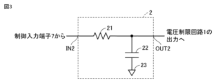
- the input node IN2 of the first variable voltage generation circuit 2 is connected to the control input terminal 7, and the output node OUT2 of the first variable voltage generation circuit 2 is connected to the output node OUT1 of the voltage limiting circuit 1.
- the first variable voltage generating circuit 2 generates a limited voltage VL, which is a voltage value limited by the voltage limiting circuit 1, when a control signal inputted to the control input terminal 7 as a turn-on operation command changes from low to high.
- a first changing voltage V1 that increases relatively slowly at a first temporal rate of change dV1/dt is generated and output to the adder circuit 5 based on .
- the first variable voltage generation circuit 2 controls the temporal change (corresponding to the first slope SL1) of the gate voltage Vg in the second region RG2 before the gate voltage Vg reaches the mirror voltage.
- the first variable voltage generation circuit 2 is configured as a first-order lag circuit including a resistance element 21 and a capacitance element 22.
- Resistance element 21 is connected between input node IN2 and output node OUT2.
- Capacitive element 22 is connected between output node OUT2 and reference node 23 that provides reference potential Vref.
- the first variable voltage generation circuit 2 includes a constant current source 24 and a capacitive element 22.
- Constant current source 24 is connected between power supply node 25 to which power supply voltage is applied and output node OUT2.
- Capacitive element 22 is connected between output node OUT2 and reference node 23.
- the constant current source 24 starts flowing a constant current to the capacitive element 22 when the control signal inputted to the control input terminal 7 as a turn-on operation command changes from low to high. Thereby, the voltage of the capacitive element 22 increases from the limit voltage VL at a constant rate of change over time.
- FIG. 5 and 6 are diagrams showing an example of the configuration of the second variable voltage generation circuit 3.
- An input node IN3 of the second variable voltage generation circuit 3 is connected to the control input terminal 7, and an output node OUT3 of the second variable voltage generation circuit 3 is connected to the comparison circuit 4 and the addition circuit 5.
- the second variable voltage generation circuit 3 generates a second voltage with reference to the reference potential Vref of the drive circuit 1000 when the control signal inputted to the control input terminal 7 as a turn-on operation command changes from low to high.
- a second changing voltage V2 that increases relatively slowly at a temporal rate of change dV2/dt is generated and output.
- the second rate of change dV2/dt is larger than the first rate of change dV1/dt described above.
- the time change of the gate voltage Vg in the third region RG3 before the gate voltage Vg reaches the mirror voltage (corresponding to the third slope SL3) is the second change output from the second change voltage generation circuit 3. It is based on the time change rate dV2/dt of voltage V2.
- the second variable voltage generation circuit 3 is configured as a first-order lag circuit including a resistance element 31 and a capacitance element 32, as in the case of FIG.
- Resistance element 31 is connected between input node IN3 and output node OUT3.
- Capacitive element 33 is connected between output node OUT3 and reference node 33 that provides reference potential Vref.
- the second variable voltage generation circuit 3 includes a constant current source 34 and a capacitive element 32, as in the case of FIG.
- Constant current source 34 is connected between power supply node 35 to which power supply voltage is applied and output node OUT3.
- Capacitive element 33 is connected between output node OUT3 and reference node 33.
- the constant current source 34 starts flowing a constant current to the capacitive element 33 when the control signal inputted to the control input terminal 7 as a turn-on operation command changes from low to high. Thereby, the voltage of the capacitive element 33 increases from the reference potential Vref at a constant time increase rate.
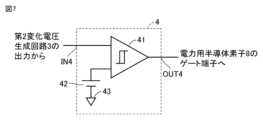
- FIG. 7 is a diagram showing an example of the configuration of the comparison circuit 4.
- the comparison circuit 4 includes a comparator 41 and a comparison voltage source 42.
- the input node IN4 of the comparison circuit 4 is connected to the output node OUT3 of the second variable voltage generation circuit 3, and the output node OUT4 of the comparison circuit 4 is connected to the gate terminal of the power semiconductor element 8.
- the non-inverting input terminal of the comparator 41 is connected to the input node IN4
- the inverting input terminal of the comparator 41 is connected to the comparison voltage source 42
- the output terminal of the comparator 41 is connected to the output node OUT4. Connected.
- the comparison circuit 4 is configured such that the second variable voltage V2 outputted from the second variable voltage generation circuit 3 is equal to the voltage value of the comparison voltage source 42 (that is, the comparison voltage VC). It outputs a low level (that is, the reference potential Vref of the drive circuit 1000) until it reaches that level, and then outputs a high level (that is, the power supply voltage of the drive circuit 1000). Thereby, the comparator circuit 4 generates a voltage that increases sharply with the fourth slope SL4, and controls the change in the gate voltage Vg in the fourth region where the gate voltage Vg is equal to or higher than the mirror voltage.
- the comparison circuit 4 may be configured to compare the first variable voltage V1 output from the first variable voltage generation circuit 2 and the comparison voltage VC. The value of the comparison voltage VC is adjusted according to the voltage change rate dV1/dt of the first change voltage V1.
- FIG. 8 is a diagram showing an example of the configuration of the adder circuit 5.
- the adder circuit 5 includes a diode 51.
- Input node IN5A of adder circuit 5 is connected to output node OUT1 of voltage limiting circuit 1 and output node OUT2 of first variable voltage generating circuit 2.
- Input node IN5B of adder circuit 5 is connected to output node OUT3 of second variable voltage generation circuit 3.
- An output node OUT5B of the adder circuit 5 is connected to an input node IN6 of the buffer circuit 6.
- Diode 51 is connected between input node IN5B and output node OUT5 so that the direction from input node IN5B to output node OUT5 is the forward direction.
- the second changing voltage V2 that increases at the second rate of change output from the second changing voltage generating circuit 3 is equal to the limiting voltage VL output from the voltage limiting circuit 1.
- the adder circuit 5 outputs the composite voltage ( VL+V1) is output. Thereafter, the adder circuit 5 outputs a current that is the sum of the output current of the voltage limiting circuit 1, the output current of the first variable voltage generation circuit 2, and the output current of the second variable voltage generation circuit 3, and outputs the combined voltage ( VL+V1) and the second variable voltage V2.
- the value of the third variable voltage V3 is determined by the characteristics of the diode 51, parasitic capacitance, and the like.
- the time rate of change dV3/dt of the third changing voltage V3 is greater than the time rate of change dV1/dt of the first changing voltage V1.
- the first period described above corresponds to a period until the second changing voltage V2 becomes equal to the sum of the limit voltage VL and the first changing voltage V1.
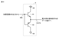
- FIG. 9, FIG. 10, and FIG. 11 are diagrams showing an example of the configuration of the buffer circuit 6.
- the buffer circuit 6 transmits the output voltage of the adder circuit 5 input via the input node IN6 to the gate of the power semiconductor element 8 via the output node OUT6, thereby increasing the gate voltage Vg of the power semiconductor element 8. generate.
- the buffer circuit 6 is configured by an emitter follower of an NPN bipolar transistor 61.
- the voltage amplification factor of the emitter follower is 1. More specifically, the collector of bipolar transistor 61 is connected to power supply node 62 to which a power supply voltage is applied, the emitter of bipolar transistor 61 is connected to output node OUT6, and the base of bipolar transistor 61 is connected to input node IN6.
- the buffer circuit 6 is configured with a push-pull type emitter follower of an NPN type bipolar transistor 61 and a PNP type bipolar transistor 63.
- the voltage amplification factor of the emitter follower is 1. More specifically, the collector of bipolar transistor 61 is connected to a power supply node 62 supplied with a power supply potential, and the collector of bipolar transistor 63 is connected to a reference node 64 supplied with reference potential Vref. Emitters of bipolar transistors 61 and 63 are connected to output node OUT6. The bases of bipolar transistors 61 and 63 are connected to input node IN6.
- the buffer circuit 6 is configured by a unity gain buffer using an operational amplifier 65. More specifically, the output terminal of the operational amplifier 65 is connected to the output node OUT6 and also to the inverting input terminal of the operational amplifier 65. A non-inverting input terminal of operational amplifier 65 is connected to input node IN6.
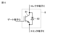
- FIG. 12 is a diagram showing an example of the configuration of the power semiconductor element 8.
- the power semiconductor element 8 is composed of an IGBT (Insulated Gate Bipolar Transistor) 81 and a freewheel diode 82.
- IGBT Insulated Gate Bipolar Transistor
- the control electrode of the power semiconductor element 8 is also referred to as a gate, and the voltage of the control electrode is also referred to as a gate voltage.
- the power semiconductor element drive circuit 1000 according to the first embodiment is characterized in that the method of controlling the gate voltage Vg of the power semiconductor element 8 is different depending on whether the collector current Ic is small or large.
- FIG. 13 is a timing chart for explaining a first operation example of the power semiconductor device drive circuit 1000 according to the first embodiment.
- FIG. 13 shows a timing diagram when the collector current Ic is relatively small during the turn-on operation of the power semiconductor element 8.
- VL+V1 second variable voltage V2 output from the second variable voltage generation circuit 3
- V3 of the adder circuit 5 judgment result of the comparator circuit 4
- gate voltage Vg of the power semiconductor element 8 collector The waveforms of current Ic and collector-emitter voltage Vce are shown.
- the case of the present embodiment is shown by a solid line
- the case of the comparative example is shown by a broken line.
- the comparative example shows a case of a constant voltage drive type or constant current drive type drive circuit that does not control the gate voltage Vg of the power semiconductor element 8 separately in a plurality of time regions.
- the voltage limiting circuit 1 At time t0, when the control signal input to the control input terminal 7 changes from low to high as a command for turn-on operation, the voltage limiting circuit 1, the first variable voltage generation circuit 2, and the second variable voltage generation circuit 3 and starts working.
- the voltage change in the gate voltage Vg in the first region RG1 near time t0 is controlled by the voltage limiting circuit 1.
- the output voltage V1 of the voltage limiting circuit 1 rapidly increases with the first slope SL1 up to the limiting voltage VL.
- the limiting voltage VL of the voltage limiting circuit 1 is set to approximately the threshold voltage Vth of the power semiconductor element 8.
- the gate voltage Vg starts to rise, but since it takes time to reach the threshold voltage Vth, the collector current Ic does not rise immediately.
- the gate voltage Vg in the first region RG1 is steeply increased to about the threshold voltage with the first slope SL1.
- the output voltage V1 of the first variable voltage generation circuit 2 starts to rise at a first temporal rate of change dV1/dt with respect to the limited voltage VL of the voltage limiting circuit 1.
- the output voltage V2 of the second variable voltage generation circuit 3 starts to rise at a second temporal rate of change dV2/dt with reference to the reference potential Vref of the drive circuit 1000.
- the rate of change dV1/dt of the first variable voltage V1 generated by the first variable voltage generating circuit 2 is higher than the rate of change dV1/dt generated by the second variable voltage generating circuit 3.
- the rate of change dV2/dt of the second changing voltage V2 is larger.
- the first change in the limiting voltage VL output from the voltage limiting circuit 1 and the first changing voltage generating circuit 2 is lower than the second changing voltage V2 output from the second changing voltage generating circuit 3. Since the sum with the voltage V1 is larger, the output voltage V3 of the adder circuit 5 becomes equal to the sum of the limit voltage VL and the first changing voltage V1.
- the determination result of the comparison circuit 4 is low (L) level because the output voltage V2 of the second variable voltage generation circuit 3 is smaller than the output voltage of the comparison voltage source 42 (that is, the comparison voltage VC).
- the collector current Ic in this embodiment starts flowing immediately because the gate voltage Vg reaches the threshold voltage Vth based on the limit voltage VL set in the voltage limit circuit 1.
- the collector current Ic in the comparative example remains 0 and does not change because the gate voltage Vg has not reached the threshold voltage Vth.
- the collector-emitter voltage Vce of the power semiconductor element 8 begins to decrease due to its rate of change dIc/dt.
- the collector-emitter voltage Vce in the comparative example does not change because the collector current Ic does not flow.
- the voltage limiting circuit 1 outputs a limited voltage VL
- the first variable voltage generation circuit 2 outputs a first variable voltage V1 that increases at a first rate of change dV1/dt. Therefore, the composite voltage (VL+V1) obtained by adding these voltages increases at the first rate of change dV1/dt with respect to the limit voltage VL.
- the output voltage V2 of the second variable voltage generation circuit 3 rises at a second rate of change dV2/dt with respect to the reference potential Vref of the drive circuit 1000.
- the output voltage V3 of the adder circuit 5 increases at the first rate of change dV1/dt with respect to the limit voltage VL, since the composite voltage (VL+V1) is larger than the second changing voltage V2.
- the determination result of the comparison circuit 4 remains low because the output voltage V2 of the second variable voltage generation circuit 3 is smaller than the comparison voltage VC.
- the gate voltage Vg in the present embodiment rapidly rises at the first slope SL1 up to the threshold voltage Vth in the first region RG1 near time t0. After that, the gate voltage Vg increases at a relatively gentle rate of change in the second region RG2 at a second slope SL2 based on the rate of change dV1/dt of the output voltage of the first variable voltage generation circuit 2.
- the gate voltage Vg in the case of the drive circuit of the comparative example reaches the threshold voltage Vth of the power semiconductor element 8 at time t1.
- the collector current Ic of the power semiconductor element 8 increases at a current change rate based on the gate voltage Vg that changes with the second slope SL2 in the second region RG2.
- Collector current Ic in the case of the drive circuit of the comparative example starts to flow because gate voltage Vg reaches threshold voltage Vth at time t1.
- the collector-emitter voltage Vce is affected by the rate of change of the collector current Ic and decreases.
- the collector-emitter voltage Vce does not change while the collector current Ic is not flowing, and starts to decrease after the collector current Ic starts flowing at time t1.
- the gate voltage Vg in this embodiment is based on the voltage change rate dV1/dt of the output voltage of the first variable voltage generation circuit 2 in the second region RG2, as in the case from time t0 to time t1. It rises relatively gently at the second slope and reaches the mirror voltage at time t2.
- the gate voltage Vg in the case of the drive circuit of the comparative example reaches the threshold voltage at time t1. Therefore, in the case of the drive circuit of the comparative example, the collector current Ic starts flowing from time t1.
- the rate of change in the gate voltage Vg in the comparative example is larger than the rate of change in the gate voltage Vg corresponding to the second slope SL2 in the second region RG2 in the present embodiment. Therefore, the rate of change dIc/dt of the collector current Ic in the case of the comparative example is larger than the rate of change dIc/dt of the collector current Ic in the case of the present embodiment.
- the switching loss of the power semiconductor element 8 in the second region RG2 becomes larger than in the case of the drive circuit of the comparative example.
- the collector current Ic is relatively small, so the influence of this loss is small.
- the output voltage V1 of the voltage limiting circuit 1 and the first variable voltage generation circuit 2, and the output voltage V2 of the second variable voltage generation circuit 3 are the same as those from time t0 to t2, so the description will not be repeated. .
- the second variable voltage V2 output from the second variable voltage generating circuit 3 is higher than the limited voltage VL output from the voltage limiting circuit.
- the sum (VL+V1) with the first variable voltage V1 output from the first variable voltage generating circuit 2 is larger. Therefore, the output voltage V3 of the adder circuit 5 is equal to the sum of the limit voltage VL and the first variable voltage V1.
- the second changing voltage V2 becomes larger than the sum (VL+V1) of the limiting voltage V and the first changing voltage V1, so the output voltage V3 of the adding circuit 5 is the sum of the limiting voltage VL and the first changing voltage V1.
- the value is based on the first changing voltage V1 and the second changing voltage V2, and the rate of change is greater than dV1/dt.
- the output current of the adder circuit 5 is equal to the sum of the output current of the voltage limiting circuit 1, the output current of the first variable voltage generation circuit 2, and the output current of the second variable voltage generation circuit 3.
- the second region RG2 is a period from after the gate voltage Vg rapidly changes with the first slope SL1 in the first region RG1 to time t3 (the above-mentioned first period).
- the gate voltage Vg reaches the mirror period in the second region RG2 where the collector current Ic of the power semiconductor element 8 is small.
- the second region RG2 includes the time for recovery after the recovery current flows (until time t3 in FIG. 13).
- the drive circuit 1000 controls the gate voltage Vg based on the first changing voltage V1 generated by the first changing voltage generating circuit 2 and having a relatively gentle voltage change rate dV1/dt. It is characterized by the fact that
- the comparative example Since the gate voltage Vg in the second region RG2 in the present embodiment changes with the second slope SL2 based on the voltage change rate dV1/dt set in the first variable voltage generation circuit 2, the comparative example The rate of change in gate voltage Vg is smaller than in the case of the drive circuit shown in FIG. 2, and the rate of change dIc/dt in collector current Ic during recovery is also smaller. As a result, the rate of change dVce/dt of the collector-emitter voltage Vce due to the recovery current also becomes smaller, so that EMI can be reduced.
- the rate of change dIc/dt of the collector current Ic in the second region RG2 in the case of the present embodiment is smaller than that in the case of the drive circuit of the comparative example.
- the collector current Ic in the present embodiment is lower than that in the drive circuit of the comparative example.
- the rate of change dIc/dt increases. In that case, EMI due to the recovery current will be larger in the case of this embodiment than in the case of the comparative example, but on the other hand, there is an advantage that switching loss in the second region RG2 can be further reduced.
- the operation of the drive circuit 1000 from time t3 to t4 in FIG. 13 will be described.
- the sum of the limited voltage VL output from the voltage limiting circuit 1 and the first variable voltage V1 output from the first variable voltage generating circuit 2 is higher than that of the second variable voltage generating circuit 3.
- the outputted second changing voltage V2 becomes larger. Therefore, the output voltage V3 of the adder circuit 5 changes based not only on the limit voltage VL and the first changing voltage V1 but also on the second changing voltage V2 after time t3.
- the third region RG3 is a period in which the gate voltage Vg is controlled mainly based on the output voltage V2 of the second variable voltage generation circuit 3. However, since the gate voltage Vg has reached the mirror period at time t2 in the second region RG2, the gate voltage Vg in the third region RG3 is constant. Similarly, in the case of the drive circuit of the comparative example, the gate voltage Vg reaches the mirror voltage at time t2, so it is constant in the third region RG3.
- the collector current Ic of the power semiconductor element 8 is constant after time t3 because the recovery current has recovered at time t3. In the case of the drive circuit of the comparative example, the collector current Ic is similarly constant after time 3.
- the collector-emitter Vce of the power semiconductor element 8 decreases at a voltage change rate dVce/dt depending on the driving ability of the buffer circuit 6. In the case of the drive circuit of the comparative example as well, the collector-emitter voltage Vce decreases at a voltage change rate depending on the drive capability of the drive circuit.
- the operation of the drive circuit 1000 from time t4 to time t5 in FIG. 13 will be described.
- the output voltage V2 of the second variable voltage generation circuit 3, which is input to the comparison circuit 4 reaches the comparison voltage VC of the comparison circuit 4.
- the determination result of the comparison circuit 4 changes from low to high.
- a current is injected into the gate terminal of the power semiconductor element 8, so that the gate voltage Vg rapidly increases at the fourth slope SL4. Note that the period from time t0 to time t4 corresponds to the aforementioned second period.
- the fourth region RG4 is a time region in which the gate voltage Vg increases with the fourth slope SL4 based on a change in the output voltage of the comparator circuit 4. That is, it is a period from the end of the mirror period of gate voltage Vg (time t4) until gate voltage Vg reaches the power supply voltage of drive circuit 1000 (time t5).
- the gate voltage Vg of the drive circuit of the comparative example remains in the mirror period from time t5 until time t6, and loss due to switching occurs during the mirror period.
- the comparison circuit 4 is used to control the gate voltage Vg in the fourth region RG4, and the gate voltage Vg is rapidly increased with the fourth slope SL4.
- the temporal rate of change dVce/dt of the collector-emitter voltage Vce can be increased, so switching loss in the fourth region RG4 can be reduced compared to the drive circuit of the comparative example.
- the drive circuit 1000 of the first embodiment is characterized in that the fourth slope SL4 in the fourth region RG4 is larger than the second slope SL2 in the second region RG2.
- the length of the mirror period depends on the magnitude of the output current of the drive circuit.
- the mirror period continues until time t6.
- the collector-emitter voltage Vce decreases to a certain constant value by time t3
- the collector-emitter voltage Vce continues to gradually decrease until time t6 when the mirror period ends. Therefore, the period from time t3 to t6 causes an increase in switching loss.
- the gate voltage Vg when the power semiconductor element 8 is turned on is divided into four time regions from the first region RG1 to the fourth region RG4. Separately controlled. Specifically, in the first region RG1, the gate voltage Vg is controlled by the voltage limiting circuit 1, and thereby rapidly rises to about the threshold voltage at the first slope SL1. As a result, dead time can be shortened and losses can be reduced.
- the gate voltage Vg is controlled by the first variable voltage generation circuit 2.
- the gate voltage Vg reaches the mirror voltage in this second region RG2. Since the rate of change of the voltage generated by the first variable voltage generation circuit 2 is smaller than the rate of change of the voltage generated by the second variable voltage generation circuit 3, the change in the collector-emitter voltage Vce due to the recovery current The ratio dVce/dt can be reduced, and as a result, EMI can be reduced.
- the gate voltage Vg is mainly controlled by the second variable voltage generation circuit 3.
- the gate voltage Vg in the second region RG2 has reached the mirror voltage, so the gate voltage Vg in the third region RG3 is constant.
- the gate voltage Vg is controlled by the output voltage of the comparator circuit 4.
- the rate of change of the gate voltage Vg in the fourth region RG4 (corresponding to the fourth slope SL4) is calculated as the rate of change of the gate voltage Vg in the second region RG2 controlled by the first variable voltage generation circuit 2 ( (corresponding to the second slope SL2).
- FIG. 14 is a timing diagram for explaining a second operation example of the power semiconductor device drive circuit 1000 according to the first embodiment.
- FIG. 14 shows a timing diagram when the collector current is relatively large during turn-on operation of the power semiconductor element 8.
- Each waveform shown in FIG. 14 corresponds to each waveform shown in FIG. 13, respectively.
- the waveforms of the gate voltage Vg, collector current Ic, and collector-emitter voltage Vce are shown by solid lines for the present embodiment, and broken lines for the comparative example.
- the comparative example shows a case of a constant voltage drive type or constant current drive type drive circuit that does not control the gate voltage Vg of the power semiconductor element 8 separately in a plurality of time regions.
- a limited voltage VL outputted from the voltage limiting circuit 1 a first changed voltage V1 outputted from the first changed voltage generation circuit 2, and a second changed voltage outputted from the second changed voltage generation circuit 3.
- V2 the output voltage V3 of the adder circuit 5, and the output of the comparator circuit 4 are the same as those from time t0 to t1.
- the gate voltage Vg in this embodiment is the voltage change rate of the output voltage V1 of the voltage limiting circuit 1 and the first variable voltage generating circuit 2 in the second region RG2, as in the case from time t0 to time t1. It increases with a relatively gentle second slope SL2 based on dV1/dt.
- the collector current Ic is relatively small as shown in FIG. 13
- the mirror voltage is also relatively small, so the gate voltage Vg reaches the mirror voltage Vm at time t2.
- the collector current Ic is relatively large as shown in FIG. 14
- the mirror voltage Vm is also relatively large, so the gate voltage Vg does not reach the mirror voltage Vm at time t2. Changes in the collector current Ic and the collector-emitter voltage Vce from time t1 to time t2 are the same as in the case of FIG. 13, so the description will not be repeated.
- the operation of the drive circuit 1000 from time t2 to t3 in FIG. 14 will be described.
- the sum of the limiting voltage VL output from the voltage limiting circuit 1 and the first changing voltage generating circuit 2 and the first changing voltage V1 is The second variable voltage V2 outputted from the second variable voltage generation circuit 3 becomes larger.
- the output voltage V3 of the adder circuit 5 is generated from the composite voltage VL+V1 generated by the voltage limiting circuit 1 and the first varying voltage generating circuit 2, and the composite voltage VL+V1 and the second varying voltage generating circuit 3.
- the voltage changes to a voltage based on the second changing voltage V2. Therefore, the rate of change in the output voltage V3 of the adder circuit 5 also changes from dV1/dt to a larger value.
- the third region RG3 is a period after the voltage change rate switches from dV1/dt to a larger change rate corresponding to the third slope SL3 as described above.
- the gate voltage Vg does not change in the third region RG3 because the gate voltage Vg reaches the mirror voltage Vm before the third region RG3.
- the collector current Ic is large as shown in FIG. 14, the gate voltage Vg has not reached the mirror voltage Vm, so the gate voltage Vg is controlled at the voltage change rate corresponding to the third slope SL3.
- the rate of change dIc/dt of the collector current Ic of the power semiconductor element 8 is based on the rate of change dV1/dt of the first variable voltage V1 generated by the first variable voltage generation circuit 2 from time t0 to t2. and change.
- the control is mainly based on the rate of change dV2/dt of the second variable voltage V2 generated by the second variable voltage generation circuit 3. Since the voltage change rate dV2/dt is larger than the voltage change rate dV1/dt, the change rate dIc/dt of the collector current Ic is also larger after time t2 than before time t2.
- the rate of change dIc/dt of the collector current Ic is constant from time t1 when the gate voltage Vg reaches the threshold voltage Vth to time t3. .
- the rate of change dIc/dt of the collector current Ic is set in two stages until time t3 when the gate voltage Vg reaches the mirror voltage Vm. Change it with. Therefore, in the second region RG2 where the rate of change dIc/dt of the collector current Ic is smaller than that of the drive circuit of the comparative example, the switching loss of the power semiconductor element 8 is larger than that of the drive circuit of the comparative example.
- the switching loss of the power semiconductor element 8 can be made equal to that of the drive circuit of the comparative example.
- the gate voltage Vg reaches the mirror voltage Vm at time t3 in the third region RG3 where the gate voltage Vg is mainly controlled by the second variable voltage generation circuit 3.
- the gate voltage Vg reaches the mirror voltage Vm at time t3.
- the collector current Ic changes because a recovery current flows.
- the collector current Ic is The rate of change dIc/dt is also the same in the present embodiment and in the comparative example. Note that the rate of change of the gate voltage Vg in the third region RG3 does not need to be the same in the present embodiment and in the comparative example.
- the operation of the drive circuit 1000 from time t4 to time t5 in FIG. 14 will be described.
- the output voltage V2 of the second variable voltage generation circuit 3, which is input to the comparison circuit 4 reaches the comparison voltage VC of the comparison circuit 4.
- the determination result of the comparison circuit 4 changes from low to high.
- the determination result of the comparator circuit 4 becomes high, a current is injected into the gate terminal of the power semiconductor element 8, so that the gate voltage Vg rapidly increases at the fourth slope SL4.
- the fourth region RG4 is a region where the gate voltage Vg changes with the fourth slope SL4 based on the change in the output voltage of the comparison circuit 4. That is, it is a period from the end of the mirror period of gate voltage Vg (time t4) until gate voltage Vg reaches the power supply voltage of drive circuit 1000 (time t5).
- the gate voltage Vg of the drive circuit of the comparative example remains in the mirror period from time t5 until time t6, and loss due to switching occurs during the mirror period.
- the operation of such a drive circuit is the same as in the case where the collector current Ic is relatively small as shown in FIG.
- the comparison circuit 4 is used to control the gate voltage Vg in the fourth region RG4, and the gate voltage Vg is rapidly increased with the fourth slope SL4.
- the rate of change dVce/dt of the collector-emitter voltage Vce can be increased, so switching loss in the fourth region RG4 can be reduced compared to the drive circuit of the comparative example.
- the rate of change of the gate voltage Vg in the fourth region RG4 i.e., the fourth slope SL4
- the rate of change of the gate voltage Vg in the second region RG2 i.e., the second slope SL4.
- the characteristic is that the slope is made larger than the slope SL2).
- the length of the mirror period depends on the magnitude of the output current of the drive circuit 1000.
- the mirror period continues until time t6.
- the collector-emitter voltage Vce decreases to a certain constant value by time t3
- the collector-emitter voltage Vce continues to gradually decrease until time t6 when the mirror period ends. Therefore, during the period from time t3 to t6, the switching loss of the power semiconductor element 8 controlled by the drive circuit of the comparative example is larger than that of the present embodiment.
- FIG. 15 is a flowchart showing a control procedure when the power semiconductor element 8 is turned on by the drive circuit 1000 of the first embodiment.
- step ST110 of FIG. 15 the drive circuit 1000, in response to the turn-on command of the power semiconductor element 8, reaches the limit voltage VL corresponding to the threshold voltage Vth of the power semiconductor element 8 in the first time domain RG1.
- the gate voltage Vg of the power semiconductor element 8 is increased by the first slope SL1.
- the drive circuit 1000 changes the gate voltage Vg from the limit voltage VL with a second slope SL2 that is gentler than the first slope SL1 in a second time domain RG2 following the first time domain RG1. increase.
- the drive circuit 1000 increases the gate voltage at a third slope SL3 that is gentler than the first slope SL1 but steeper than the second slope SL2.
- Vg is increased to the mirror voltage Vm.
- the drive circuit 1000 turns off the power semiconductor when the first period described above has elapsed after receiving the turn-on command, regardless of whether the gate voltage Vg has reached the mirror voltage Vm.
- the rate of increase in the voltage supplied to the gate terminal of element 8 is increased. However, if the mirror period is entered before the first period elapses, the effect of the increase in the voltage increase rate does not appear as a change in the gate voltage.
- the drive circuit 1000 increases the gate voltage from the mirror voltage at a fourth slope SL4 that is steeper than the third slope SL3 in the fourth time domain RG4. Eventually, the gate voltage Vg increases to the power supply voltage supplied to the drive circuit 1000.
- the gate voltage Vg when the power semiconductor element 8 is turned on is controlled in four time regions from the first region RG1 to the fourth region RG4. be done. Specifically, in the first region RG1, the gate voltage Vg is controlled by the voltage limiting circuit 1, and thereby rapidly increases to about the threshold voltage at the first slope SL1. As a result, dead time can be shortened and losses can be reduced.
- the gate voltage Vg is controlled by the first variable voltage generation circuit 2.
- the gate voltage Vg reaches the mirror voltage in this second region RG2. Since the rate of change of the voltage generated by the first variable voltage generation circuit 2 is smaller than the rate of change of the voltage generated by the second variable voltage generation circuit 3, the change in the collector-emitter voltage Vce due to the recovery current The ratio dVce/dt can be reduced, and as a result, EMI can be reduced.
- the gate voltage Vg reaches the mirror voltage in this third region RG3.
- the gate voltage Vg is increased by the third slope SL3 mainly using the second variable voltage generation circuit 3. Since this third slope SL3 is larger than the second slope SL2, which is the rate of change of the gate voltage Vg in the second region RG2, the rate of change dIc/dt of the collector current Ic can be increased, resulting in a loss can suppress the increase in
- the gate voltage Vg is controlled by the output voltage of the comparator circuit 4.
- the rate of change of the gate voltage Vg at this time is made larger than the rate of voltage change in the second region RG2 controlled by the second variable voltage generation circuit 3.
- FIG. 16 is a diagram illustrating an example of a mounting aspect of the drive circuit 1000 of the first embodiment. As shown in FIG. 16, the drive circuit 1000 of Embodiment 1 and the power module 10000 configured with the power semiconductor element 8 can be combined. In this way, the drive circuit 1000 of the first embodiment may be configured separately from the power module 10000 configured with the power semiconductor element 8.
- FIG. 17 is a diagram showing a modification of the implementation shown in FIG. 16.
- the drive circuit 1000 of Embodiment 1 may be included inside a power module 10000a configured with a power semiconductor element 8. That is, power module 10000a includes drive circuit 1000 of Embodiment 1 and power semiconductor element 8.
- FIG. 18 is a diagram showing another example of the implementation of the drive circuit 1000 of the first embodiment.
- FIG. 18 shows a more specific implementation example of a drive circuit 1000 combined with a three-phase AC power module 10000b. That is, six drive circuits 1000un, 1000vn, 1000wn, 1000up, 1000vp, and 1000wp are mounted to drive a power module 10000b composed of six power semiconductor elements. Note that the number of power semiconductor elements included in one power module is not particularly limited. That is, configurations such as 1in1, 2in1, 6in1, and multiple parallel configurations can be used as the power module.
- FIG. 18 shows a power module 10000b with a 6-in-1 configuration.
- the power module 10000b includes power semiconductor elements 8up, 8vp, 8wp, 8un, 8vn, and 8wn.
- Each power semiconductor element 8 includes an IGBT 81 (81up, 81vp, 81wp, 81un, 81vn, 81wn) and a diode 82 (82up, 82vp, 82wp, 82un, 82vn, 82wn) connected in antiparallel thereto.
- the U-phase power semiconductor elements 8up and 8un are connected in series between the P terminal and the Q terminal.
- a connection node between the power semiconductor elements 8up and 8un is connected to the U terminal.
- the gates of power semiconductor elements 8up and 8un are connected to drive circuits 1000up and 1000un, respectively.
- the drive circuits 1000up and 1000un are provided with control input terminals UP and UN, respectively.
- u (or U) may be replaced with v, w (or V, W).
- FIG. 19 is a diagram showing a modification of the implementation shown in FIG. 18.
- six drive circuits 1000un, 1000vn, 1000wn, 1000up, 1000vp, and 1000wp are installed inside a power module 10000c composed of power semiconductor elements 8up, 8vp, 8wp, 8un, 8vn, and 8wn. May contain. That is, the power module 10000c includes the six drive circuits 1000un, 1000vn, 1000wn, 1000up, 1000vp, and 1000wp of the first embodiment, and their corresponding power semiconductor elements 8up, 8vp, 8wp, 8un, 8vn, and 8wn. Equipped with.
- the number of power semiconductor elements included in one power module is not particularly limited. That is, configurations such as 1in1, 2in1, 6in1, and multiple parallel configurations can be used as the power module.
- One power module includes the same number of drive circuits as power semiconductor elements.
- Embodiment 2 The power semiconductor device drive circuit 2000 of the second embodiment differs from the drive circuit 1000 of the first embodiment in that it further includes a mirror voltage detection circuit 9 that detects a mirror voltage.
- a mirror voltage detection circuit 9 that detects a mirror voltage.
- FIG. 20 is a diagram showing the configuration of a power semiconductor device drive circuit 2000 according to the second embodiment.
- Drive circuit 2000 in FIG. 20 like drive circuit 1000 in Embodiment 1, generates gate voltage Vg for controlling switching of power semiconductor element 8 according to a control signal input to control input terminal 7. . More specifically, the drive circuit 1000 sequentially controls the voltage change of the gate voltage Vg during the turn-on operation of the power semiconductor element 8 in four time domains from the first region RG1 to the fourth region RG4.
- the third region RG3 may not be provided and the second region RG2 may directly transition to the fourth region RG4.
- the drive circuit 2000 has the same configuration as the drive circuit 1000 of Embodiment 1, and includes a voltage limiting circuit 1, a first variable voltage generation circuit 2, and a second variable voltage generation circuit 3. , a comparison circuit 4, an addition circuit 5, and a buffer circuit 6.
- the voltage limiting circuit 1 controls the voltage change of the gate voltage Vg in the first region.
- the first variable voltage generation circuit 2 controls the voltage change of the gate voltage Vg in the second region.
- the second variable voltage generation circuit 3 controls the voltage change of the gate voltage Vg in the third region.
- Comparison circuit 4 controls the voltage change of gate voltage Vg in the fourth region.
- Adder circuit 5 outputs the current and voltage output from voltage limiting circuit 1 and first variable voltage generating circuit 2 in second region RG2.
- the adding circuit 5 adds the output current of the second variable voltage generation circuit 3 to the output current of the voltage limiting circuit 1 and the first variable voltage generation circuit 2 in the third region RG3.
- Buffer circuit 6 generates a gate voltage of power semiconductor element 8 by transmitting the output voltage of adder circuit 5 to the gate terminal of power semiconductor element 8 .
- the drive circuit 2000 includes a mirror voltage detection circuit 9 as a new configuration.
- the mirror voltage detection circuit 9 detects the timing when the gate voltage Vg reaches the mirror voltage, and outputs the detection result to the comparison circuit 4.
- Comparison circuit 4 compares the detection result of mirror voltage detection circuit 9 and the output voltage of comparison voltage source 42 (ie, comparison voltage VC), and outputs the comparison result. Specifically, when the output of the mirror voltage detection circuit 9 is activated to a high level, the high level output signal of the mirror voltage detection circuit 9 is higher than the comparison voltage VC. Therefore, in this case, the comparison circuit 4 outputs the power supply voltage of the drive circuit 2000 as a high-level signal to the gate terminal of the power semiconductor element 8.
- the problem with the drive circuit 1000 of the first embodiment in which the mirror voltage detection circuit 9 is not provided is as follows. That is, in the drive circuit 1000 of the first embodiment, the timing of transition to the fourth region is controlled according to the set value of the comparison voltage of the comparison circuit 4. More specifically, the comparison circuit 4 compares the comparison voltage VC (that is, the voltage value of the comparison voltage source 42) and the output voltage V2 of the second variable voltage generation circuit 3, and determines whether the output voltage V2 is equal to or higher than the comparison voltage VC. When , the voltage change rate of the gate voltage Vg is changed by moving to the fourth region.
- the gate voltage control in the fourth region is started at a timing that depends on the rate of change of the voltage V2 generated by the second variable voltage generation circuit 3, the magnitude of the collector current Ic of the power semiconductor element is Even if the magnitude of the mirror voltage and the length of the mirror period change, the timing at which gate voltage control is started in the fourth region does not change. Therefore, in the drive circuit 1000 of the first embodiment, as the collector current Ic becomes smaller, the time from when the gate voltage reaches the mirror voltage to when controlling the gate voltage in the fourth region is started becomes longer. As a result, the effect of reducing switching loss by controlling the rate of change of the gate voltage in the fourth region and increasing the rate of change dVce/dt of the collector-emitter voltage Vce becomes small. In the drive circuit 2000 of the second embodiment, the above problem is solved.
- FIG. 21 is a diagram showing an example of the configuration of the mirror voltage detection circuit 9.
- the mirror voltage detection circuit 9 includes a differentiation circuit 91, a binarization circuit 92, an edge detection circuit 93, a flip-flop circuit 94, and an inversion circuit 95.
- the differentiator circuit 91, the binarization circuit 92, and the edge detection circuit 93 are connected in this order between the input node IN9A and the S input of the flip-flop circuit 94.
- Input node IN9A is connected to the gate terminal of power semiconductor element 8.
- Inverting circuit 95 is connected between input node IN9B and the R input of flip-flop circuit 94.
- Input node IN9B is connected to control input terminal 7.
- the Q output of the flip-flop circuit 94 is connected to the input node IN4 of the comparison circuit 4 via the output node OUT9.
- the mirror voltage detection circuit 9 detects the mirror voltage generated in the gate signal Vg of the power semiconductor element 8 by a differentiating circuit 91, a binarization circuit 92, and an edge detection circuit 93, and holds the detected state by a flip-flop circuit 94. do. Further, the inversion circuit 95 of the mirror voltage detection circuit 9 inverts the control signal input from the control input terminal 7. The inverted control signal is used to reset the flip-flop circuit 94. Therefore, the mirror voltage detection circuit 9 detects the mirror voltage and holds the detection result when the control signal is at high level, and resets the held detection result when the control signal becomes low level.
- Differentiator circuit 91 differentiates gate voltage Vg of power semiconductor element 8 and outputs the differentiated signal to binarization circuit 92 .
- the differentiating circuit 91 includes a capacitive element 911 and a resistive element 912.
- Capacitive element 911 is connected between input node IN91 and output node OUT91.
- Resistance element 912 is connected between output node OUT91 and reference node 913 to which reference potential Vref is applied.
- Input node IN91 is connected to the gate terminal of power semiconductor element 8, and output node OUT91 is connected to the input of binarization circuit 92.
- the differentiating circuit 91 includes a resistive element 914, a capacitive element 915, and an operational amplifier 916.
- Resistance element 914 is connected between the inverting input terminal of operational amplifier 916 and the output terminal of operational amplifier 916.
- Capacitive element 915 is connected between the inverting input terminal of operational amplifier 916 and input node IN91A.
- the reference potential Vref of the drive circuit 2000 is input to the non-inverting input terminal of the operational amplifier 916 via the input node IN91B.
- the output terminal of operational amplifier 916 is connected to the input of binarization circuit 92 via output node OUT91.
- FIG. 24 is a diagram showing an example of the configuration of the binarization circuit 92.
- the binarization circuit 92 converts the output of the differentiating circuit 91 into binary values of high level and low level, and outputs the converted binarized signal to the edge detection circuit 93.
- the edge detection circuit 93 is configured by an inverted Schmitt trigger circuit 921 (also referred to as a Schmitt trigger inverter or a hysteresis inverter).
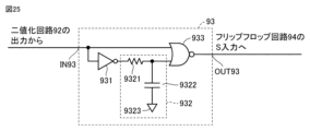
- FIG. 25 is a diagram showing an example of the configuration of the edge detection circuit 93.
- Edge detection circuit 93 detects a rising edge or a falling edge of the output signal of binarization circuit 92 and outputs a detection result. Whether a rising edge or a falling edge is detected can be changed depending on the polarity of the binarization circuit 92 or the polarity detected by the flip-flop circuit 94. A suitable edge is selected.
- the edge detection circuit 93 includes an inversion circuit (inverter) 931, a delay circuit 932, and a NOR circuit 933.
- the delay circuit 932 includes, for example, a resistive element 9321 and a capacitive element 9322.
- Input node IN93 of edge detection circuit 93 is connected to a first input terminal of NOR circuit 933, and also connected to a second input terminal of NOR circuit 933 via inverting circuit 931 and delay circuit 932 in this order.
- Resistance element 9321 of delay circuit 932 is connected between the output terminal of inversion circuit 931 and the second input terminal of NOR circuit 933.
- Capacitive element 9322 of delay circuit 932 is connected between the second input terminal of NOR circuit 933 and reference node 9323 to which reference potential Vref is applied.
- An input node IN93 of the edge detection circuit 93 is connected to the output of the binarization circuit 92.
- the output terminal of NOR circuit 933 is connected to the S input node of flip-flop circuit 94 via output node OUT93.
- FIG. 26 is a diagram showing an example of the configuration of the flip-flop circuit 94.
- Flip-flop circuit 94 includes two NOR circuits 941 and 942.
- a first input terminal of the NOR circuit 941 is connected as a set terminal S to an output node OUT93 of the edge detection circuit 93.
- a second input terminal of NOR circuit 941 is connected to an output terminal of NOR circuit 942.
- An output terminal of NOR circuit 941 is connected to a first input terminal of NOR circuit 942.
- a second input terminal of the NOR circuit 942 is connected to the output of the inversion circuit 95 as a reset terminal R.
- the output terminal of the NOR circuit 942 is connected to the input of the comparison circuit 4 as the output terminal Q of the flip-flop circuit 94.
- the flip-flop circuit 94 is activated by inputting the signal detected by the edge detection circuit 93 to the set terminal S, and by inputting the control signal inverted by the inverting circuit 95 to the reset terminal R. becomes inactive.
- FIG. 27 shows an example of the configuration of the inversion circuit 95.
- Inversion circuit 95 includes a NOT circuit 951.
- the inverting circuit 95 inverts the polarity of the control signal input from the control input terminal 7 and outputs the inverted control signal to the reset terminal R of the flip-flop circuit 94. As a result, the state held by the flip-flop circuit 94 is reset.
- FIG. 28 is a timing diagram for explaining an example of the operation of the power semiconductor drive circuit 2000 according to the second embodiment.
- FIG. 28 shows a timing diagram when the collector current Ic is relatively small during the turn-on operation of the power semiconductor element 8. From the top of FIG. 28, the control signal input to the control input terminal 7, the limited voltage VL output from the voltage limiting circuit 1, and the first variable voltage V1 output from the first variable voltage generation circuit 2 are shown in order from the top of FIG.
- the waveforms of the output of the mirror voltage detection circuit 9, the output of the determination result of the comparison circuit 4, the collector current Ic of the power semiconductor element 8, and the collector-emitter voltage Vce are shown.
- the case of the present embodiment is shown by a solid line
- the case of the comparative example is shown by a broken line.
- the comparative example shows a case of a constant voltage drive type or constant current drive type drive circuit that does not control the gate voltage Vg of the power semiconductor element 8 separately in a plurality of time regions.
- the power semiconductor element drive circuit 2000 controls the power semiconductor element 8 when the collector current Ic is relatively small and when the collector current Ic is relatively large. They are characterized by different methods of controlling collector current Ic and collector-emitter voltage Vce.
- the drive circuit 2000 of the second embodiment differences from the operation of the drive circuit 1000 of the first embodiment shown in FIG. 13 when the collector current is relatively small will be explained.
- the voltage limiting circuit 1 and the first changing voltage generating circuit 2 starts operating.
- the voltage change in the gate voltage Vg in the first region RG1 near time t0 is controlled by the voltage limiting circuit 1.
- the voltage limiting circuit 1 rapidly increases the gate voltage Vg in the first region RG1 with the first slope SL1 to approximately the threshold voltage Vth (corresponding to the limiting voltage VL). let This makes it possible to shorten dead time and reduce loss.
- the operation of drive circuit 2000 from time t0 to time t2 is almost the same as the operation of drive circuit 1000 of the first embodiment shown in FIG. 13. That is, the output composite voltage VL+V1 of the voltage limiting circuit 1 and the first variable voltage generation circuit 2, the output voltage V2 of the second variable voltage generation circuit 3, the output voltage V3 of the adder circuit 5, the collector current Ic, and the collector-emitter
- the waveform of the voltage Vce is the same as that of the drive circuit 1000 of the first embodiment shown in FIG.
- the flip-flop circuit 94 is in an inactive state until time t2 because the gate voltage Vg has not reached the mirror voltage Vm. Therefore, the output of mirror voltage detection circuit 9 is also at low (L) level.
- gate voltage Vg reaches mirror voltage Vm.
- the mirror voltage detection circuit 9 operates, and the differentiating circuit 91, the binarization circuit 92, and the edge detection circuit 93 detect the timing when the gate voltage Vg reaches the mirror voltage. Since a delay time occurs in the timing detection by the differentiator circuit 91, the binarization circuit 92, and the edge detection circuit 93, the set signal of the flip-flop circuit 94 changes from low to high at time t3, which is a certain period of time after time t2. do.
- the delay time that occurs in timing detection by the differentiator circuit 91, the binarization circuit 92, and the edge detection circuit 93 can be arbitrarily designed by the designer as a design parameter. Therefore, the designer can also arbitrarily design the interval from the timing when the gate voltage Vg reaches the mirror voltage Vm to the next operation, which is the timing when the comparison circuit 4 adjusts the rate of change of the gate voltage Vg.
- the output of the mirror voltage detection circuit 9 changes from low to high and maintains that state. Furthermore, when the output of the mirror voltage detection circuit 9 changes from low to high at time t3, the determination result of the comparison circuit 4 also changes from low to high.
- the determination result of the comparison circuit 4 becomes high, a current is injected into the gate terminal of the power semiconductor element 8, so that the gate voltage Vg rapidly increases at the fourth slope SL4. That is, in the example of FIG. 28, the second region RG2 directly transitions to the fourth region RG4 without passing through the third region RG3.
- the rate of change dVce/dt of the collector-emitter voltage Vce can be increased, so switching loss can be reduced.
- the gate voltage Vg controlled by the drive circuit of the comparative example is still in the mirror period, and loss due to switching occurs during the mirror period. Furthermore, in the case of the drive circuit 1000 of the first embodiment shown in FIG. , the timing at which the output of the comparison circuit 4 switches from low to high is determined. Therefore, depending on the setting of the comparison voltage, the timing at which the output of the comparison circuit 4 switches from low to high is delayed compared to the case of the drive circuit 2000 of the second embodiment.
- the mirror voltage detection circuit 9 detects the timing when the gate voltage Vg reaches the mirror voltage Vm.
- the comparison circuit 4 can be operated according to the detection result.
- the drive circuit 2000 of the second embodiment can have smaller loss than the drive circuit 1000 of the first embodiment.
- the set signal of the flip-flop circuit 94 changes to high at time t3, and then falls from high to low at time t4 in accordance with the operation of the edge detection circuit 93.
- the period during which the edge detection circuit 93 maintains a high level can be arbitrarily designed by a designer. Therefore, the period during which the edge detection circuit 93 maintains a high level can be arbitrarily set depending on the length of time during which the flip-flop circuit 94 can operate and the frequency at which the power semiconductor element 8 is operated.
- the reset signal of the flip-flop circuit 94 changes to high level.
- the state held by the flip-flop circuit 94 is reset. That is, the output of the mirror voltage detection circuit 9 and the determination result of the comparison circuit 4 both change from high to low. This completes the injection of current into the gate terminal of the power semiconductor element 8.
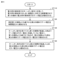
- FIG. 29 is a flowchart showing a control procedure when the power semiconductor element 8 is turned on by the drive circuit 2000 of the second embodiment.
- step ST110 of FIG. 29 the drive circuit 2000, in response to the turn-on command of the power semiconductor element 8, reaches the limit voltage VL corresponding to the threshold voltage Vth of the power semiconductor element 8 in the first time domain RG1.
- the gate voltage Vg of the power semiconductor element 8 is increased by the first slope SL1.
- the drive circuit 2000 changes the gate voltage Vg from the limit voltage VL with a second slope SL2 that is gentler than the first slope SL1 in a second time domain RG2 following the first time domain RG1. increase.
- step ST125 the drive circuit 2000 increases the gate voltage from the mirror voltage by a fourth slope SL4 that is steeper than the third slope SL3. Eventually, the gate voltage Vg increases to the power supply voltage supplied to the drive circuit 2000.
- step ST125 if the mirror voltage detection circuit 9 does not detect that the gate voltage Vg has reached the mirror voltage Vm after the first period has elapsed since receiving the turn-on command (NO in step ST125), The process proceeds to step ST130.
- step ST130 the drive circuit 2000 sets a third slope that is gentler than the first slope SL1 but steeper than the second slope SL2 in the third time domain RG3 following the second time domain RG2.
- the gate voltage Vg is increased to the mirror voltage Vm.
- the gate voltage Vg when the power semiconductor element 8 is turned on is basically the same as the drive circuit 1000 of the first embodiment.
- Control is divided into four time regions from a first region RG1 to a fourth region RG4.
- the gate voltage Vg is controlled by the voltage limiting circuit 1, and thereby rapidly increases to about the threshold voltage at the first slope SL1. This can shorten dead time and reduce loss.
- the gate voltage Vg is controlled by the first variable voltage generation circuit 2.
- the gate voltage Vg reaches the mirror voltage in this second region RG2. Since the rate of change of the voltage generated by the first variable voltage generation circuit 2 (corresponding to the second slope SL2) is smaller than the rate of change of the voltage generated by the second variable voltage generation circuit 3, recovery is possible.
- the rate of change dVce/dt of the collector-emitter voltage Vce due to current can be reduced, and as a result, EMI can be reduced.
- the next control in the third region RG3 is executed when the collector current Ic flowing through the power semiconductor element 8 is relatively large.
- the gate voltage Vg reaches the mirror voltage halfway through the third region RG3.
- the second variable voltage generation circuit 3 is used to control the gate voltage Vg to increase at the third slope SL3, which is larger than the second slope SL2. be done.
- the rate of change dIc/dt of the collector current Ic can be increased, thereby suppressing an increase in loss.
- the next control in the fourth region RG4 is executed based on the mirror voltage detection circuit 9 detecting the timing at which the gate voltage Vg reaches the mirror voltage Vm.
- the comparator circuit 4 By operating the comparator circuit 4 in response to detecting the timing at which the mirror voltage Vm is reached, the rate of change dVce/dt of the collector-emitter voltage Vce can be increased, and switching loss can be reduced. Since the comparison circuit 4 operates based on the detection result of the mirror voltage detection circuit 9, the switching loss is lower than in the case of the drive circuit 1000 of the first embodiment, in which the timing at which the comparison circuit 4 operates is delayed as the mirror voltage becomes smaller. can be reduced.
Landscapes
- Power Conversion In General (AREA)
- Engineering & Computer Science (AREA)
- Power Engineering (AREA)
Priority Applications (5)
| Application Number | Priority Date | Filing Date | Title |
|---|---|---|---|
| US18/858,758 US20250274031A1 (en) | 2022-05-17 | 2022-05-17 | Driving circuit and driving method for power semiconductor element, and power module |
| PCT/JP2022/020535 WO2023223426A1 (ja) | 2022-05-17 | 2022-05-17 | 電力用半導体素子の駆動回路および駆動方法ならびにパワーモジュール |
| DE112022007234.2T DE112022007234T5 (de) | 2022-05-17 | 2022-05-17 | Treiberschaltung und Ansteuerverfahren für ein Leistungshalbleiterelement und Leistungsmodul |
| JP2024521430A JPWO2023223426A1 (https=) | 2022-05-17 | 2022-05-17 | |
| CN202280095748.7A CN119156770A (zh) | 2022-05-17 | 2022-05-17 | 电力用半导体元件的驱动电路及驱动方法以及功率模块 |
Applications Claiming Priority (1)
| Application Number | Priority Date | Filing Date | Title |
|---|---|---|---|
| PCT/JP2022/020535 WO2023223426A1 (ja) | 2022-05-17 | 2022-05-17 | 電力用半導体素子の駆動回路および駆動方法ならびにパワーモジュール |
Publications (1)
| Publication Number | Publication Date |
|---|---|
| WO2023223426A1 true WO2023223426A1 (ja) | 2023-11-23 |
Family
ID=88834842
Family Applications (1)
| Application Number | Title | Priority Date | Filing Date |
|---|---|---|---|
| PCT/JP2022/020535 Ceased WO2023223426A1 (ja) | 2022-05-17 | 2022-05-17 | 電力用半導体素子の駆動回路および駆動方法ならびにパワーモジュール |
Country Status (5)
| Country | Link |
|---|---|
| US (1) | US20250274031A1 (https=) |
| JP (1) | JPWO2023223426A1 (https=) |
| CN (1) | CN119156770A (https=) |
| DE (1) | DE112022007234T5 (https=) |
| WO (1) | WO2023223426A1 (https=) |
Cited By (1)
| Publication number | Priority date | Publication date | Assignee | Title |
|---|---|---|---|---|
| CN118353340A (zh) * | 2024-06-18 | 2024-07-16 | 上海泰矽微电子有限公司 | 马达驱动电路、芯片和车辆设备 |
Citations (2)
| Publication number | Priority date | Publication date | Assignee | Title |
|---|---|---|---|---|
| JP2018029258A (ja) * | 2016-08-17 | 2018-02-22 | 株式会社デンソー | トランジスタ駆動回路 |
| WO2018198426A1 (ja) * | 2017-04-26 | 2018-11-01 | 三菱電機株式会社 | 半導体素子の駆動方法および駆動装置、ならびに、電力変換装置 |
Family Cites Families (14)
| Publication number | Priority date | Publication date | Assignee | Title |
|---|---|---|---|---|
| US7667524B2 (en) | 2004-11-05 | 2010-02-23 | International Rectifier Corporation | Driver circuit and method with reduced DI/DT and having delay compensation |
| JP5138287B2 (ja) * | 2007-06-27 | 2013-02-06 | 三菱電機株式会社 | ゲート駆動装置 |
| JP5065986B2 (ja) * | 2008-05-12 | 2012-11-07 | 日立オートモティブシステムズ株式会社 | 半導体装置の駆動装置及びその駆動方法 |
| JP5447575B2 (ja) * | 2012-04-23 | 2014-03-19 | 株式会社デンソー | 駆動装置 |
| JP6197685B2 (ja) * | 2014-02-19 | 2017-09-20 | 株式会社デンソー | ゲート駆動回路 |
| EP3057231B1 (de) * | 2015-02-16 | 2019-04-10 | Power Integrations Switzerland GmbH | Steuerschaltung und Steuerverfahren zum Anschalten eines Leistungshalbleiterschalters |
| CN105356727B (zh) * | 2015-11-27 | 2018-11-27 | 矽力杰半导体技术(杭州)有限公司 | 用于开关电源的开关管驱动控制方法以及控制电路 |
| US9813055B2 (en) * | 2016-04-01 | 2017-11-07 | Ixys Corporation | Gate driver that drives with a sequence of gate resistances |
| JP6836342B2 (ja) * | 2016-06-22 | 2021-02-24 | ルネサスエレクトロニクス株式会社 | 駆動装置および電力供給システム |
| JP6870240B2 (ja) * | 2016-08-31 | 2021-05-12 | 富士電機株式会社 | ゲート駆動装置 |
| US10491207B2 (en) * | 2017-09-07 | 2019-11-26 | Infineon Technologies Austria Ag | Method of over current and over voltage protection of a power switch in combination with regulated DI/DT and DV/DT |
| JP7000968B2 (ja) * | 2018-04-05 | 2022-01-19 | 株式会社デンソー | スイッチの駆動回路 |
| US11695409B2 (en) * | 2019-04-09 | 2023-07-04 | Mitsubishi Electric Corporation | Drive circuit of power semiconductor element |
| JP7180626B2 (ja) * | 2020-03-03 | 2022-11-30 | 株式会社デンソー | ゲート駆動装置 |
-
2022
- 2022-05-17 WO PCT/JP2022/020535 patent/WO2023223426A1/ja not_active Ceased
- 2022-05-17 JP JP2024521430A patent/JPWO2023223426A1/ja active Pending
- 2022-05-17 US US18/858,758 patent/US20250274031A1/en active Pending
- 2022-05-17 DE DE112022007234.2T patent/DE112022007234T5/de not_active Withdrawn
- 2022-05-17 CN CN202280095748.7A patent/CN119156770A/zh active Pending
Patent Citations (2)
| Publication number | Priority date | Publication date | Assignee | Title |
|---|---|---|---|---|
| JP2018029258A (ja) * | 2016-08-17 | 2018-02-22 | 株式会社デンソー | トランジスタ駆動回路 |
| WO2018198426A1 (ja) * | 2017-04-26 | 2018-11-01 | 三菱電機株式会社 | 半導体素子の駆動方法および駆動装置、ならびに、電力変換装置 |
Cited By (1)
| Publication number | Priority date | Publication date | Assignee | Title |
|---|---|---|---|---|
| CN118353340A (zh) * | 2024-06-18 | 2024-07-16 | 上海泰矽微电子有限公司 | 马达驱动电路、芯片和车辆设备 |
Also Published As
| Publication number | Publication date |
|---|---|
| DE112022007234T5 (de) | 2025-03-13 |
| CN119156770A (zh) | 2024-12-17 |
| US20250274031A1 (en) | 2025-08-28 |
| JPWO2023223426A1 (https=) | 2023-11-23 |
Similar Documents
| Publication | Publication Date | Title |
|---|---|---|
| Camacho et al. | A novel active gate driver for improving SiC MOSFET switching trajectory | |
| US9979292B2 (en) | Control method and control circuit for switch in switching power supply | |
| CN103208984B (zh) | 有源栅极驱动电路 | |
| EP3108580B1 (en) | Multi-stage gate turn-off with dynamic timing | |
| JP6362996B2 (ja) | 半導体駆動装置ならびにそれを用いた電力変換装置 | |
| US5986484A (en) | Semiconductor device drive circuit with voltage surge suppression | |
| US9813055B2 (en) | Gate driver that drives with a sequence of gate resistances | |
| JP4991446B2 (ja) | 電力変換装置 | |
| EP3952082A1 (en) | Semiconductor device, power conversion device using same, and driving method for semiconductor device | |
| US9843263B2 (en) | Systems and methods for driving a bipolar junction transistor by adjusting base current with time | |
| WO2020109777A1 (en) | Gate driver | |
| WO2023223426A1 (ja) | 電力用半導体素子の駆動回路および駆動方法ならびにパワーモジュール | |
| EP3322093B1 (en) | Gate trajectory control for zero overshoot switching | |
| CN115769476B (zh) | 电力用半导体元件的驱动调整电路、功率模块以及电力变换装置 | |
| JP7218836B2 (ja) | 半導体素子の駆動能力切替回路及び半導体素子の駆動装置 | |
| CN117081553A (zh) | 一种主动抑制SiC MOSFET关断电压尖峰和振荡的电路 | |
| Zhang et al. | An improved gate driver based on magnetic coupling for crosstalk suppression of SiC devices | |
| JP2023093292A (ja) | ゲート駆動装置 | |
| JP6004988B2 (ja) | 電力用半導体素子のゲート制御装置 | |
| JPWO2023223426A5 (https=) | ||
| US12519465B2 (en) | Systems and methods for gate current shaping for gate drivers | |
| Wang et al. | Repetitive control strategy of SiC MOSFET to reduce EMI generation | |
| Gomez-Rivera et al. | Analysis of a Gate-Driving Technique for Enhancing the GaN Power Transistors Performance | |
| JP6921263B1 (ja) | 電力変換回路 | |
| KR101242985B1 (ko) | 멀티 스테이지 능동 구동 드라이버. |
Legal Events
| Date | Code | Title | Description |
|---|---|---|---|
| 121 | Ep: the epo has been informed by wipo that ep was designated in this application |
Ref document number: 22942631 Country of ref document: EP Kind code of ref document: A1 |
|
| ENP | Entry into the national phase |
Ref document number: 2024521430 Country of ref document: JP Kind code of ref document: A |
|
| WWE | Wipo information: entry into national phase |
Ref document number: 18858758 Country of ref document: US |
|
| WWE | Wipo information: entry into national phase |
Ref document number: 202280095748.7 Country of ref document: CN |
|
| WWE | Wipo information: entry into national phase |
Ref document number: 112022007234 Country of ref document: DE |
|
| WWP | Wipo information: published in national office |
Ref document number: 112022007234 Country of ref document: DE |
|
| 122 | Ep: pct application non-entry in european phase |
Ref document number: 22942631 Country of ref document: EP Kind code of ref document: A1 |
|
| WWP | Wipo information: published in national office |
Ref document number: 18858758 Country of ref document: US |