WO2023223426A1 - 電力用半導体素子の駆動回路および駆動方法ならびにパワーモジュール - Google Patents
電力用半導体素子の駆動回路および駆動方法ならびにパワーモジュール Download PDFInfo
- Publication number
- WO2023223426A1 WO2023223426A1 PCT/JP2022/020535 JP2022020535W WO2023223426A1 WO 2023223426 A1 WO2023223426 A1 WO 2023223426A1 JP 2022020535 W JP2022020535 W JP 2022020535W WO 2023223426 A1 WO2023223426 A1 WO 2023223426A1
- Authority
- WO
- WIPO (PCT)
- Prior art keywords
- voltage
- circuit
- power semiconductor
- gate
- slope
- Prior art date
Links
- 239000004065 semiconductor Substances 0.000 title claims abstract description 158
- 238000000034 method Methods 0.000 title claims description 19
- 230000004044 response Effects 0.000 claims abstract description 10
- 230000008859 change Effects 0.000 claims description 137
- 238000001514 detection method Methods 0.000 claims description 40
- 238000003708 edge detection Methods 0.000 claims description 22
- 230000004069 differentiation Effects 0.000 claims description 2
- 238000010586 diagram Methods 0.000 description 47
- 230000000052 comparative effect Effects 0.000 description 46
- 230000007423 decrease Effects 0.000 description 10
- 238000011084 recovery Methods 0.000 description 10
- 239000002131 composite material Substances 0.000 description 6
- 230000002123 temporal effect Effects 0.000 description 6
- BNPSSFBOAGDEEL-UHFFFAOYSA-N albuterol sulfate Chemical compound OS(O)(=O)=O.CC(C)(C)NCC(O)C1=CC=C(O)C(CO)=C1.CC(C)(C)NCC(O)C1=CC=C(O)C(CO)=C1 BNPSSFBOAGDEEL-UHFFFAOYSA-N 0.000 description 4
- 238000006243 chemical reaction Methods 0.000 description 4
- 230000003111 delayed effect Effects 0.000 description 4
- 230000000694 effects Effects 0.000 description 4
- 230000004048 modification Effects 0.000 description 4
- 238000012986 modification Methods 0.000 description 4
- 230000007704 transition Effects 0.000 description 3
- 230000003321 amplification Effects 0.000 description 2
- 238000003199 nucleic acid amplification method Methods 0.000 description 2
- 230000008569 process Effects 0.000 description 2
- 230000000630 rising effect Effects 0.000 description 2
- 230000008901 benefit Effects 0.000 description 1
- 230000005669 field effect Effects 0.000 description 1
- 239000005431 greenhouse gas Substances 0.000 description 1
- 238000002347 injection Methods 0.000 description 1
- 239000007924 injection Substances 0.000 description 1
- 230000003071 parasitic effect Effects 0.000 description 1
- 230000009467 reduction Effects 0.000 description 1
- 238000013519 translation Methods 0.000 description 1
- 230000014616 translation Effects 0.000 description 1
Images


Classifications
-
- H—ELECTRICITY
- H03—ELECTRONIC CIRCUITRY
- H03K—PULSE TECHNIQUE
- H03K17/00—Electronic switching or gating, i.e. not by contact-making and –breaking
- H03K17/16—Modifications for eliminating interference voltages or currents
Definitions
- the present disclosure relates to a drive circuit and a drive method for a power semiconductor element, and a power module.
- Power semiconductor devices that control large amounts of power are used, for example, in power supply circuits that generate alternating current with different frequencies from direct current and alternating current, and in power converters having power supply circuits.
- a power semiconductor element is used in a power conversion device such as an inverter, it is important to suppress power consumption from the viewpoint of energy saving and greenhouse gas reduction.
- Patent Document 1 discloses a method of reducing energy consumed by a power semiconductor element by controlling switching of the power semiconductor element.
- this document describes "a method for driving a power transistor switch, comprising the steps of receiving a drive input signal, converting the drive input signal to a conversion drive input signal, and using the conversion drive input signal to control the switch.
- the conversion drive input signal has three regions in time, each having a slope, the first region being the Miller Plateau of the switch.
- the second region is the time when there is a second slope consisting of a smaller slope compared to the first slope
- the third region is the time when there is a third slope larger than the second slope.
- control electrode voltage quickly reaches the Miller plateau voltage, then slowly reaches the threshold voltage of the switch, and then, when the switch is almost fully turned on, the control electrode voltage
- the switch delay time is maintained substantially constant by adjusting the transistor control electrode precharge voltage.
- Patent Document 1 According to the control method for a power semiconductor device disclosed in the above-mentioned Japanese translations of PCT publication No. 2008-519529 (Patent Document 1), EMI (electromagnetic interference) is reduced by reducing the current change rate (dI/dt) during switching. can be lowered. However, if the current change rate is controlled to be small when the current I flowing through the power semiconductor element is large, there is a problem in that switching time increases and switching loss increases. The above patent documents do not consider this point.
- the present disclosure has been made in consideration of the above problems, and one of the purposes is to provide a power semiconductor device that can suppress switching loss even when a relatively large current flows through the power semiconductor device.
- An object of the present invention is to provide a driving circuit for an element.
- a drive circuit for a power semiconductor device includes a first gate voltage control circuit and a second gate voltage control circuit.
- the first gate voltage control circuit controls the power semiconductor device in different manners in the order of a first time domain, a second time domain, and a third time domain in response to a turn-on command of the power semiconductor device.
- the gate voltage is made to reach the mirror voltage.
- the gate voltage reaches the mirror voltage in the second time domain or in the third time domain, depending on the magnitude of the main current flowing through the power semiconductor element.
- the second gate voltage control circuit controls a gate voltage equal to or higher than the mirror voltage.
- the drive circuit operates in different manners in the first time domain, the second time domain, and the third time domain in response to the turn-on command of the power semiconductor device.
- the gate voltage is made to reach the mirror voltage. Therefore, switching loss can be suppressed even when the current flowing through the power semiconductor element is relatively large.
- FIG. 1 is a block diagram showing the configuration of a drive circuit for a power semiconductor device according to a first embodiment
- FIG. FIG. 3 is a diagram showing an example of the configuration of a voltage limiting circuit.
- FIG. 3 is a diagram illustrating an example of the configuration of a first variable voltage generation circuit.
- FIG. 3 is a diagram illustrating an example of the configuration of a first variable voltage generation circuit.
- FIG. 3 is a diagram illustrating an example of the configuration of a second variable voltage generation circuit.
- FIG. 3 is a diagram illustrating an example of the configuration of a second variable voltage generation circuit.
- FIG. 3 is a diagram showing an example of the configuration of a comparison circuit.
- FIG. 3 is a diagram showing an example of the configuration of an adder circuit.
- FIG. 3 is a diagram showing an example of the configuration of an adder circuit.
- FIG. 3 is a diagram showing an example of the configuration of a buffer circuit.
- FIG. 3 is a diagram showing an example of the configuration of a buffer circuit.
- FIG. 3 is a diagram showing an example of the configuration of a buffer circuit.
- FIG. 1 is a diagram showing an example of the configuration of a power semiconductor element.
- FIG. 2 is a timing chart for explaining a first operation example of the power semiconductor element drive circuit according to the first embodiment.
- 7 is a timing chart for explaining a second operation example of the power semiconductor device drive circuit according to the first embodiment.
- FIG. 5 is a flowchart showing a control procedure when the power semiconductor device is turned on by the drive circuit of the first embodiment.
- FIG. 3 is a diagram showing an example of a mounting aspect of the drive circuit according to the first embodiment.
- FIG. 17 is a diagram showing a modification of the implementation mode of FIG. 16.
- FIG. 7 is a diagram illustrating another example of the implementation mode of the drive circuit of the first embodiment.
- FIG. 19 is a diagram showing a modification of the implementation mode of FIG. 18.
- FIG. 7 is a diagram showing the configuration of a drive circuit for a power semiconductor element according to a second embodiment.
- FIG. 2 is a diagram showing an example of the configuration of a mirror voltage detection circuit.
- FIG. 2 is a diagram showing an example of the configuration of a differentiating circuit.
- FIG. 2 is a diagram showing an example of the configuration of a differentiating circuit.
- FIG. 2 is a diagram showing an example of the configuration of a binarization circuit.
- FIG. 3 is a diagram showing an example of the configuration of an edge detection circuit.
- FIG. 2 is a diagram showing an example of the configuration of a flip-flop circuit. This is an example of a configuration of an inverting circuit.
- FIG. 7 is a timing diagram for explaining an example of the operation of the power semiconductor drive circuit according to the second embodiment. 7 is a flowchart showing a control procedure when the power semiconductor device is turned on by the drive circuit according to the second embodiment.
- FIG. 1 is a block diagram showing the configuration of a power semiconductor device drive circuit 1000 according to the first embodiment.
- Drive circuit 1000 generates gate voltage Vg for controlling switching of power semiconductor element 8 according to a control signal input to control input terminal 7 . More specifically, the drive circuit 1000 sequentially changes the voltage change of the gate voltage Vg during the turn-on operation of the power semiconductor element 8 from the first time domain (RG1 in FIGS. 13 and 14) to the fourth time domain (RG1 in FIGS. 13 and 14). Control is performed in four time domains up to RG4) in FIGS. 13 and 14.
- the first to fourth time regions are also simply referred to as first to fourth regions.
- the drive circuit 1000 includes a voltage limiting circuit 1, a first variable voltage generation circuit 2, a second variable voltage generation circuit 3, a comparison circuit 4, an addition circuit 5, and a buffer circuit. 6.
- the voltage limiting circuit 1, the first variable voltage generation circuit 2, the second variable voltage generation circuit 3, the addition circuit 5, and the buffer circuit 6 are collectively referred to as a first gate voltage control circuit 10.
- the first gate voltage control circuit 10 controls the power semiconductor element 8 in different ways in the order of a first time domain RG1, a second time domain RG2, and a third time domain RG3 in response to the turn-on command.
- the gate voltage Vg is made to reach the mirror voltage Vm.
- the gate voltage Vg reaches the mirror voltage Vm in the second region RG2 or the third region RG3.
- Comparison circuit 4 as a second gate voltage control circuit controls gate voltage Vg after the mirror period. The functions of each circuit are briefly described below.
- the voltage limiting circuit 1 controls the voltage change of the gate voltage Vg in the first region RG1. Specifically, the voltage limiting circuit 1 outputs a limiting voltage VL (also referred to as a first voltage) in response to a turn-on command, thereby increasing the voltage up to the limiting voltage VL at a first slope (SL1 in FIGS. 13 and 14). Rapidly increase gate voltage Vg. That is, the voltage limiting circuit 1 limits the gate voltage Vg to the limit voltage VL when the power semiconductor element 8 rises.
- the limit voltage VL corresponds to the threshold voltage Vth of the power semiconductor element 8 and has a value approximately equal to the threshold voltage Vth.
- the first variable voltage generation circuit 2 controls the voltage change of the gate voltage Vg in the second region RG2. Specifically, the first variable voltage generation circuit 2 generates the first variable voltage V1 that increases at a second slope (SL2 in FIGS. 13 and 14) that is gentler than the first slope SL1. The first variable voltage generation circuit 2 supplies the generated first variable voltage V1 to the gate of the power semiconductor element 8 via the buffer circuit 6, thereby changing the gate voltage Vg from the limit voltage VL to a second slope. Increase at SL2.
- the second variable voltage generation circuit 3 controls the voltage change of the gate voltage Vg in the third region RG3. Specifically, the second variable voltage generation circuit 3 generates a second variable voltage V2 that changes more steeply than the first variable voltage V1 output from the first variable voltage generation circuit 2. As a result, if the gate voltage Vg has not reached the mirror voltage when the first period (from time t0 to t3 in FIG. 13, from time t0 to t2 in FIG. 14) has elapsed after receiving the turn-on command, At a third slope SL3 that is gentler than the first slope SL1 but steeper than the second slope SL2, the gate voltage Vg increases to the mirror voltage.
- the comparison circuit 4 controls the voltage change of the gate voltage Vg in the fourth region RG4. Specifically, the comparator circuit 4 calculates a fourth slope steeper than the third slope SL3 from the time when a second period (from time t0 to t4 in FIGS. 13 and 14) has elapsed after receiving the turn-on command. The gate voltage Vg is increased from the mirror voltage by the slope SL4. Eventually, the gate voltage Vg reaches the power supply voltage supplied to the drive circuit 1000.
- the adder circuit 5 outputs a voltage obtained by adding the first variable voltage V1 to the limited voltage VL until the above-mentioned first period has elapsed after receiving the turn-on command.
- the adder circuit 5 adjusts the output current of the voltage limiting circuit 1, the output current of the first variable voltage generation circuit 2, and the output current of the second variable voltage generation circuit from the time when the above-mentioned first period has elapsed after receiving the turn-on command. 3, and outputs a third variable voltage V3 based on the above-described limited voltage VL, first variable voltage V1, and second variable voltage V2.
- Buffer circuit 6 generates gate voltage Vg of power semiconductor element 8 by transmitting the output voltage of adder circuit 5 to the gate of power semiconductor element 8 .
- the first region RG1 corresponds to the time when the gate voltage Vg rises immediately after receiving the turn-on command.
- the second region RG2 is a time region from when the gate voltage Vg rises until the above-mentioned first period elapses.
- the third region RG3 is a time region from the elapse of the first period to the elapse of the second period.
- the fourth region RG4 is a time region from when the second period described above passes until the gate voltage Vg reaches the power supply voltage of the drive circuit 1000.
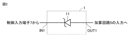
- FIG. 2 is a diagram showing an example of the configuration of the voltage limiting circuit 1.
- the voltage limiting circuit 1 includes, for example, a Zener diode 11.
- an input node IN1 of the voltage limiting circuit 1 is connected to a control input terminal 7 for controlling the power semiconductor element 8 from the outside.
- the output node OUT1 of the voltage limiting circuit 1 is connected to the adding circuit 5.
- the cathode of the Zener diode 11 is connected to the input node IN1, and the anode of the Zener diode 11 is connected to the output node OUT1.
- the voltage limiting circuit 1 controls the voltage change of the output node OUT1 when the control signal inputted to the control input terminal 7 as a turn-on operation command changes from low to high. Restrict. Specifically, the voltage at the output node OUT1 of the voltage limiting circuit 1 does not change until the voltage at the input node IN1 of the voltage limiting circuit 1 reaches the Zener voltage of the Zener diode 11 (hereinafter also referred to as limiting voltage VL), and then is limited to the Zener voltage. Thereby, the voltage limiting circuit 1 generates a voltage that changes rapidly and controls the voltage change of the gate voltage Vg in the first region RG1.
- the input node IN2 of the first variable voltage generation circuit 2 is connected to the control input terminal 7, and the output node OUT2 of the first variable voltage generation circuit 2 is connected to the output node OUT1 of the voltage limiting circuit 1.
- the first variable voltage generating circuit 2 generates a limited voltage VL, which is a voltage value limited by the voltage limiting circuit 1, when a control signal inputted to the control input terminal 7 as a turn-on operation command changes from low to high.
- a first changing voltage V1 that increases relatively slowly at a first temporal rate of change dV1/dt is generated and output to the adder circuit 5 based on .
- the first variable voltage generation circuit 2 controls the temporal change (corresponding to the first slope SL1) of the gate voltage Vg in the second region RG2 before the gate voltage Vg reaches the mirror voltage.
- the first variable voltage generation circuit 2 is configured as a first-order lag circuit including a resistance element 21 and a capacitance element 22.
- Resistance element 21 is connected between input node IN2 and output node OUT2.
- Capacitive element 22 is connected between output node OUT2 and reference node 23 that provides reference potential Vref.
- the first variable voltage generation circuit 2 includes a constant current source 24 and a capacitive element 22.
- Constant current source 24 is connected between power supply node 25 to which power supply voltage is applied and output node OUT2.
- Capacitive element 22 is connected between output node OUT2 and reference node 23.
- the constant current source 24 starts flowing a constant current to the capacitive element 22 when the control signal inputted to the control input terminal 7 as a turn-on operation command changes from low to high. Thereby, the voltage of the capacitive element 22 increases from the limit voltage VL at a constant rate of change over time.
- FIG. 5 and 6 are diagrams showing an example of the configuration of the second variable voltage generation circuit 3.
- An input node IN3 of the second variable voltage generation circuit 3 is connected to the control input terminal 7, and an output node OUT3 of the second variable voltage generation circuit 3 is connected to the comparison circuit 4 and the addition circuit 5.
- the second variable voltage generation circuit 3 generates a second voltage with reference to the reference potential Vref of the drive circuit 1000 when the control signal inputted to the control input terminal 7 as a turn-on operation command changes from low to high.
- a second changing voltage V2 that increases relatively slowly at a temporal rate of change dV2/dt is generated and output.
- the second rate of change dV2/dt is larger than the first rate of change dV1/dt described above.
- the time change of the gate voltage Vg in the third region RG3 before the gate voltage Vg reaches the mirror voltage (corresponding to the third slope SL3) is the second change output from the second change voltage generation circuit 3. It is based on the time change rate dV2/dt of voltage V2.
- the second variable voltage generation circuit 3 is configured as a first-order lag circuit including a resistance element 31 and a capacitance element 32, as in the case of FIG.
- Resistance element 31 is connected between input node IN3 and output node OUT3.
- Capacitive element 33 is connected between output node OUT3 and reference node 33 that provides reference potential Vref.
- the second variable voltage generation circuit 3 includes a constant current source 34 and a capacitive element 32, as in the case of FIG.
- Constant current source 34 is connected between power supply node 35 to which power supply voltage is applied and output node OUT3.
- Capacitive element 33 is connected between output node OUT3 and reference node 33.
- the constant current source 34 starts flowing a constant current to the capacitive element 33 when the control signal inputted to the control input terminal 7 as a turn-on operation command changes from low to high. Thereby, the voltage of the capacitive element 33 increases from the reference potential Vref at a constant time increase rate.
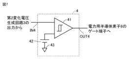
- FIG. 7 is a diagram showing an example of the configuration of the comparison circuit 4.
- the comparison circuit 4 includes a comparator 41 and a comparison voltage source 42.
- the input node IN4 of the comparison circuit 4 is connected to the output node OUT3 of the second variable voltage generation circuit 3, and the output node OUT4 of the comparison circuit 4 is connected to the gate terminal of the power semiconductor element 8.
- the non-inverting input terminal of the comparator 41 is connected to the input node IN4
- the inverting input terminal of the comparator 41 is connected to the comparison voltage source 42
- the output terminal of the comparator 41 is connected to the output node OUT4. Connected.
- the comparison circuit 4 is configured such that the second variable voltage V2 outputted from the second variable voltage generation circuit 3 is equal to the voltage value of the comparison voltage source 42 (that is, the comparison voltage VC). It outputs a low level (that is, the reference potential Vref of the drive circuit 1000) until it reaches that level, and then outputs a high level (that is, the power supply voltage of the drive circuit 1000). Thereby, the comparator circuit 4 generates a voltage that increases sharply with the fourth slope SL4, and controls the change in the gate voltage Vg in the fourth region where the gate voltage Vg is equal to or higher than the mirror voltage.
- the comparison circuit 4 may be configured to compare the first variable voltage V1 output from the first variable voltage generation circuit 2 and the comparison voltage VC. The value of the comparison voltage VC is adjusted according to the voltage change rate dV1/dt of the first change voltage V1.
- FIG. 8 is a diagram showing an example of the configuration of the adder circuit 5.
- the adder circuit 5 includes a diode 51.
- Input node IN5A of adder circuit 5 is connected to output node OUT1 of voltage limiting circuit 1 and output node OUT2 of first variable voltage generating circuit 2.
- Input node IN5B of adder circuit 5 is connected to output node OUT3 of second variable voltage generation circuit 3.
- An output node OUT5B of the adder circuit 5 is connected to an input node IN6 of the buffer circuit 6.
- Diode 51 is connected between input node IN5B and output node OUT5 so that the direction from input node IN5B to output node OUT5 is the forward direction.
- the second changing voltage V2 that increases at the second rate of change output from the second changing voltage generating circuit 3 is equal to the limiting voltage VL output from the voltage limiting circuit 1.
- the adder circuit 5 outputs the composite voltage ( VL+V1) is output. Thereafter, the adder circuit 5 outputs a current that is the sum of the output current of the voltage limiting circuit 1, the output current of the first variable voltage generation circuit 2, and the output current of the second variable voltage generation circuit 3, and outputs the combined voltage ( VL+V1) and the second variable voltage V2.
- the value of the third variable voltage V3 is determined by the characteristics of the diode 51, parasitic capacitance, and the like.
- the time rate of change dV3/dt of the third changing voltage V3 is greater than the time rate of change dV1/dt of the first changing voltage V1.
- the first period described above corresponds to a period until the second changing voltage V2 becomes equal to the sum of the limit voltage VL and the first changing voltage V1.
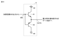
- FIG. 9, FIG. 10, and FIG. 11 are diagrams showing an example of the configuration of the buffer circuit 6.
- the buffer circuit 6 transmits the output voltage of the adder circuit 5 input via the input node IN6 to the gate of the power semiconductor element 8 via the output node OUT6, thereby increasing the gate voltage Vg of the power semiconductor element 8. generate.
- the buffer circuit 6 is configured by an emitter follower of an NPN bipolar transistor 61.
- the voltage amplification factor of the emitter follower is 1. More specifically, the collector of bipolar transistor 61 is connected to power supply node 62 to which a power supply voltage is applied, the emitter of bipolar transistor 61 is connected to output node OUT6, and the base of bipolar transistor 61 is connected to input node IN6.
- the buffer circuit 6 is configured with a push-pull type emitter follower of an NPN type bipolar transistor 61 and a PNP type bipolar transistor 63.
- the voltage amplification factor of the emitter follower is 1. More specifically, the collector of bipolar transistor 61 is connected to a power supply node 62 supplied with a power supply potential, and the collector of bipolar transistor 63 is connected to a reference node 64 supplied with reference potential Vref. Emitters of bipolar transistors 61 and 63 are connected to output node OUT6. The bases of bipolar transistors 61 and 63 are connected to input node IN6.
- the buffer circuit 6 is configured by a unity gain buffer using an operational amplifier 65. More specifically, the output terminal of the operational amplifier 65 is connected to the output node OUT6 and also to the inverting input terminal of the operational amplifier 65. A non-inverting input terminal of operational amplifier 65 is connected to input node IN6.
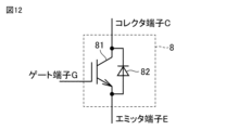
- FIG. 12 is a diagram showing an example of the configuration of the power semiconductor element 8.
- the power semiconductor element 8 is composed of an IGBT (Insulated Gate Bipolar Transistor) 81 and a freewheel diode 82.
- IGBT Insulated Gate Bipolar Transistor
- the control electrode of the power semiconductor element 8 is also referred to as a gate, and the voltage of the control electrode is also referred to as a gate voltage.
- the power semiconductor element drive circuit 1000 according to the first embodiment is characterized in that the method of controlling the gate voltage Vg of the power semiconductor element 8 is different depending on whether the collector current Ic is small or large.
- FIG. 13 is a timing chart for explaining a first operation example of the power semiconductor device drive circuit 1000 according to the first embodiment.
- FIG. 13 shows a timing diagram when the collector current Ic is relatively small during the turn-on operation of the power semiconductor element 8.
- VL+V1 second variable voltage V2 output from the second variable voltage generation circuit 3
- V3 of the adder circuit 5 judgment result of the comparator circuit 4
- gate voltage Vg of the power semiconductor element 8 collector The waveforms of current Ic and collector-emitter voltage Vce are shown.
- the case of the present embodiment is shown by a solid line
- the case of the comparative example is shown by a broken line.
- the comparative example shows a case of a constant voltage drive type or constant current drive type drive circuit that does not control the gate voltage Vg of the power semiconductor element 8 separately in a plurality of time regions.
- the voltage limiting circuit 1 At time t0, when the control signal input to the control input terminal 7 changes from low to high as a command for turn-on operation, the voltage limiting circuit 1, the first variable voltage generation circuit 2, and the second variable voltage generation circuit 3 and starts working.
- the voltage change in the gate voltage Vg in the first region RG1 near time t0 is controlled by the voltage limiting circuit 1.
- the output voltage V1 of the voltage limiting circuit 1 rapidly increases with the first slope SL1 up to the limiting voltage VL.
- the limiting voltage VL of the voltage limiting circuit 1 is set to approximately the threshold voltage Vth of the power semiconductor element 8.
- the gate voltage Vg starts to rise, but since it takes time to reach the threshold voltage Vth, the collector current Ic does not rise immediately.
- the gate voltage Vg in the first region RG1 is steeply increased to about the threshold voltage with the first slope SL1.
- the output voltage V1 of the first variable voltage generation circuit 2 starts to rise at a first temporal rate of change dV1/dt with respect to the limited voltage VL of the voltage limiting circuit 1.
- the output voltage V2 of the second variable voltage generation circuit 3 starts to rise at a second temporal rate of change dV2/dt with reference to the reference potential Vref of the drive circuit 1000.
- the rate of change dV1/dt of the first variable voltage V1 generated by the first variable voltage generating circuit 2 is higher than the rate of change dV1/dt generated by the second variable voltage generating circuit 3.
- the rate of change dV2/dt of the second changing voltage V2 is larger.
- the first change in the limiting voltage VL output from the voltage limiting circuit 1 and the first changing voltage generating circuit 2 is lower than the second changing voltage V2 output from the second changing voltage generating circuit 3. Since the sum with the voltage V1 is larger, the output voltage V3 of the adder circuit 5 becomes equal to the sum of the limit voltage VL and the first changing voltage V1.
- the determination result of the comparison circuit 4 is low (L) level because the output voltage V2 of the second variable voltage generation circuit 3 is smaller than the output voltage of the comparison voltage source 42 (that is, the comparison voltage VC).
- the collector current Ic in this embodiment starts flowing immediately because the gate voltage Vg reaches the threshold voltage Vth based on the limit voltage VL set in the voltage limit circuit 1.
- the collector current Ic in the comparative example remains 0 and does not change because the gate voltage Vg has not reached the threshold voltage Vth.
- the collector-emitter voltage Vce of the power semiconductor element 8 begins to decrease due to its rate of change dIc/dt.
- the collector-emitter voltage Vce in the comparative example does not change because the collector current Ic does not flow.
- the voltage limiting circuit 1 outputs a limited voltage VL
- the first variable voltage generation circuit 2 outputs a first variable voltage V1 that increases at a first rate of change dV1/dt. Therefore, the composite voltage (VL+V1) obtained by adding these voltages increases at the first rate of change dV1/dt with respect to the limit voltage VL.
- the output voltage V2 of the second variable voltage generation circuit 3 rises at a second rate of change dV2/dt with respect to the reference potential Vref of the drive circuit 1000.
- the output voltage V3 of the adder circuit 5 increases at the first rate of change dV1/dt with respect to the limit voltage VL, since the composite voltage (VL+V1) is larger than the second changing voltage V2.
- the determination result of the comparison circuit 4 remains low because the output voltage V2 of the second variable voltage generation circuit 3 is smaller than the comparison voltage VC.
- the gate voltage Vg in the present embodiment rapidly rises at the first slope SL1 up to the threshold voltage Vth in the first region RG1 near time t0. After that, the gate voltage Vg increases at a relatively gentle rate of change in the second region RG2 at a second slope SL2 based on the rate of change dV1/dt of the output voltage of the first variable voltage generation circuit 2.
- the gate voltage Vg in the case of the drive circuit of the comparative example reaches the threshold voltage Vth of the power semiconductor element 8 at time t1.
- the collector current Ic of the power semiconductor element 8 increases at a current change rate based on the gate voltage Vg that changes with the second slope SL2 in the second region RG2.
- Collector current Ic in the case of the drive circuit of the comparative example starts to flow because gate voltage Vg reaches threshold voltage Vth at time t1.
- the collector-emitter voltage Vce is affected by the rate of change of the collector current Ic and decreases.
- the collector-emitter voltage Vce does not change while the collector current Ic is not flowing, and starts to decrease after the collector current Ic starts flowing at time t1.
- the gate voltage Vg in this embodiment is based on the voltage change rate dV1/dt of the output voltage of the first variable voltage generation circuit 2 in the second region RG2, as in the case from time t0 to time t1. It rises relatively gently at the second slope and reaches the mirror voltage at time t2.
- the gate voltage Vg in the case of the drive circuit of the comparative example reaches the threshold voltage at time t1. Therefore, in the case of the drive circuit of the comparative example, the collector current Ic starts flowing from time t1.
- the rate of change in the gate voltage Vg in the comparative example is larger than the rate of change in the gate voltage Vg corresponding to the second slope SL2 in the second region RG2 in the present embodiment. Therefore, the rate of change dIc/dt of the collector current Ic in the case of the comparative example is larger than the rate of change dIc/dt of the collector current Ic in the case of the present embodiment.
- the switching loss of the power semiconductor element 8 in the second region RG2 becomes larger than in the case of the drive circuit of the comparative example.
- the collector current Ic is relatively small, so the influence of this loss is small.
- the output voltage V1 of the voltage limiting circuit 1 and the first variable voltage generation circuit 2, and the output voltage V2 of the second variable voltage generation circuit 3 are the same as those from time t0 to t2, so the description will not be repeated. .
- the second variable voltage V2 output from the second variable voltage generating circuit 3 is higher than the limited voltage VL output from the voltage limiting circuit.
- the sum (VL+V1) with the first variable voltage V1 output from the first variable voltage generating circuit 2 is larger. Therefore, the output voltage V3 of the adder circuit 5 is equal to the sum of the limit voltage VL and the first variable voltage V1.
- the second changing voltage V2 becomes larger than the sum (VL+V1) of the limiting voltage V and the first changing voltage V1, so the output voltage V3 of the adding circuit 5 is the sum of the limiting voltage VL and the first changing voltage V1.
- the value is based on the first changing voltage V1 and the second changing voltage V2, and the rate of change is greater than dV1/dt.
- the output current of the adder circuit 5 is equal to the sum of the output current of the voltage limiting circuit 1, the output current of the first variable voltage generation circuit 2, and the output current of the second variable voltage generation circuit 3.
- the second region RG2 is a period from after the gate voltage Vg rapidly changes with the first slope SL1 in the first region RG1 to time t3 (the above-mentioned first period).
- the gate voltage Vg reaches the mirror period in the second region RG2 where the collector current Ic of the power semiconductor element 8 is small.
- the second region RG2 includes the time for recovery after the recovery current flows (until time t3 in FIG. 13).
- the drive circuit 1000 controls the gate voltage Vg based on the first changing voltage V1 generated by the first changing voltage generating circuit 2 and having a relatively gentle voltage change rate dV1/dt. It is characterized by the fact that
- the comparative example Since the gate voltage Vg in the second region RG2 in the present embodiment changes with the second slope SL2 based on the voltage change rate dV1/dt set in the first variable voltage generation circuit 2, the comparative example The rate of change in gate voltage Vg is smaller than in the case of the drive circuit shown in FIG. 2, and the rate of change dIc/dt in collector current Ic during recovery is also smaller. As a result, the rate of change dVce/dt of the collector-emitter voltage Vce due to the recovery current also becomes smaller, so that EMI can be reduced.
- the rate of change dIc/dt of the collector current Ic in the second region RG2 in the case of the present embodiment is smaller than that in the case of the drive circuit of the comparative example.
- the collector current Ic in the present embodiment is lower than that in the drive circuit of the comparative example.
- the rate of change dIc/dt increases. In that case, EMI due to the recovery current will be larger in the case of this embodiment than in the case of the comparative example, but on the other hand, there is an advantage that switching loss in the second region RG2 can be further reduced.
- the operation of the drive circuit 1000 from time t3 to t4 in FIG. 13 will be described.
- the sum of the limited voltage VL output from the voltage limiting circuit 1 and the first variable voltage V1 output from the first variable voltage generating circuit 2 is higher than that of the second variable voltage generating circuit 3.
- the outputted second changing voltage V2 becomes larger. Therefore, the output voltage V3 of the adder circuit 5 changes based not only on the limit voltage VL and the first changing voltage V1 but also on the second changing voltage V2 after time t3.
- the third region RG3 is a period in which the gate voltage Vg is controlled mainly based on the output voltage V2 of the second variable voltage generation circuit 3. However, since the gate voltage Vg has reached the mirror period at time t2 in the second region RG2, the gate voltage Vg in the third region RG3 is constant. Similarly, in the case of the drive circuit of the comparative example, the gate voltage Vg reaches the mirror voltage at time t2, so it is constant in the third region RG3.
- the collector current Ic of the power semiconductor element 8 is constant after time t3 because the recovery current has recovered at time t3. In the case of the drive circuit of the comparative example, the collector current Ic is similarly constant after time 3.
- the collector-emitter Vce of the power semiconductor element 8 decreases at a voltage change rate dVce/dt depending on the driving ability of the buffer circuit 6. In the case of the drive circuit of the comparative example as well, the collector-emitter voltage Vce decreases at a voltage change rate depending on the drive capability of the drive circuit.
- the operation of the drive circuit 1000 from time t4 to time t5 in FIG. 13 will be described.
- the output voltage V2 of the second variable voltage generation circuit 3, which is input to the comparison circuit 4 reaches the comparison voltage VC of the comparison circuit 4.
- the determination result of the comparison circuit 4 changes from low to high.
- a current is injected into the gate terminal of the power semiconductor element 8, so that the gate voltage Vg rapidly increases at the fourth slope SL4. Note that the period from time t0 to time t4 corresponds to the aforementioned second period.
- the fourth region RG4 is a time region in which the gate voltage Vg increases with the fourth slope SL4 based on a change in the output voltage of the comparator circuit 4. That is, it is a period from the end of the mirror period of gate voltage Vg (time t4) until gate voltage Vg reaches the power supply voltage of drive circuit 1000 (time t5).
- the gate voltage Vg of the drive circuit of the comparative example remains in the mirror period from time t5 until time t6, and loss due to switching occurs during the mirror period.
- the comparison circuit 4 is used to control the gate voltage Vg in the fourth region RG4, and the gate voltage Vg is rapidly increased with the fourth slope SL4.
- the temporal rate of change dVce/dt of the collector-emitter voltage Vce can be increased, so switching loss in the fourth region RG4 can be reduced compared to the drive circuit of the comparative example.
- the drive circuit 1000 of the first embodiment is characterized in that the fourth slope SL4 in the fourth region RG4 is larger than the second slope SL2 in the second region RG2.
- the length of the mirror period depends on the magnitude of the output current of the drive circuit.
- the mirror period continues until time t6.
- the collector-emitter voltage Vce decreases to a certain constant value by time t3
- the collector-emitter voltage Vce continues to gradually decrease until time t6 when the mirror period ends. Therefore, the period from time t3 to t6 causes an increase in switching loss.
- the gate voltage Vg when the power semiconductor element 8 is turned on is divided into four time regions from the first region RG1 to the fourth region RG4. Separately controlled. Specifically, in the first region RG1, the gate voltage Vg is controlled by the voltage limiting circuit 1, and thereby rapidly rises to about the threshold voltage at the first slope SL1. As a result, dead time can be shortened and losses can be reduced.
- the gate voltage Vg is controlled by the first variable voltage generation circuit 2.
- the gate voltage Vg reaches the mirror voltage in this second region RG2. Since the rate of change of the voltage generated by the first variable voltage generation circuit 2 is smaller than the rate of change of the voltage generated by the second variable voltage generation circuit 3, the change in the collector-emitter voltage Vce due to the recovery current The ratio dVce/dt can be reduced, and as a result, EMI can be reduced.
- the gate voltage Vg is mainly controlled by the second variable voltage generation circuit 3.
- the gate voltage Vg in the second region RG2 has reached the mirror voltage, so the gate voltage Vg in the third region RG3 is constant.
- the gate voltage Vg is controlled by the output voltage of the comparator circuit 4.
- the rate of change of the gate voltage Vg in the fourth region RG4 (corresponding to the fourth slope SL4) is calculated as the rate of change of the gate voltage Vg in the second region RG2 controlled by the first variable voltage generation circuit 2 ( (corresponding to the second slope SL2).
- FIG. 14 is a timing diagram for explaining a second operation example of the power semiconductor device drive circuit 1000 according to the first embodiment.
- FIG. 14 shows a timing diagram when the collector current is relatively large during turn-on operation of the power semiconductor element 8.
- Each waveform shown in FIG. 14 corresponds to each waveform shown in FIG. 13, respectively.
- the waveforms of the gate voltage Vg, collector current Ic, and collector-emitter voltage Vce are shown by solid lines for the present embodiment, and broken lines for the comparative example.
- the comparative example shows a case of a constant voltage drive type or constant current drive type drive circuit that does not control the gate voltage Vg of the power semiconductor element 8 separately in a plurality of time regions.
- a limited voltage VL outputted from the voltage limiting circuit 1 a first changed voltage V1 outputted from the first changed voltage generation circuit 2, and a second changed voltage outputted from the second changed voltage generation circuit 3.
- V2 the output voltage V3 of the adder circuit 5, and the output of the comparator circuit 4 are the same as those from time t0 to t1.
- the gate voltage Vg in this embodiment is the voltage change rate of the output voltage V1 of the voltage limiting circuit 1 and the first variable voltage generating circuit 2 in the second region RG2, as in the case from time t0 to time t1. It increases with a relatively gentle second slope SL2 based on dV1/dt.
- the collector current Ic is relatively small as shown in FIG. 13
- the mirror voltage is also relatively small, so the gate voltage Vg reaches the mirror voltage Vm at time t2.
- the collector current Ic is relatively large as shown in FIG. 14
- the mirror voltage Vm is also relatively large, so the gate voltage Vg does not reach the mirror voltage Vm at time t2. Changes in the collector current Ic and the collector-emitter voltage Vce from time t1 to time t2 are the same as in the case of FIG. 13, so the description will not be repeated.
- the operation of the drive circuit 1000 from time t2 to t3 in FIG. 14 will be described.
- the sum of the limiting voltage VL output from the voltage limiting circuit 1 and the first changing voltage generating circuit 2 and the first changing voltage V1 is The second variable voltage V2 outputted from the second variable voltage generation circuit 3 becomes larger.
- the output voltage V3 of the adder circuit 5 is generated from the composite voltage VL+V1 generated by the voltage limiting circuit 1 and the first varying voltage generating circuit 2, and the composite voltage VL+V1 and the second varying voltage generating circuit 3.
- the voltage changes to a voltage based on the second changing voltage V2. Therefore, the rate of change in the output voltage V3 of the adder circuit 5 also changes from dV1/dt to a larger value.
- the third region RG3 is a period after the voltage change rate switches from dV1/dt to a larger change rate corresponding to the third slope SL3 as described above.
- the gate voltage Vg does not change in the third region RG3 because the gate voltage Vg reaches the mirror voltage Vm before the third region RG3.
- the collector current Ic is large as shown in FIG. 14, the gate voltage Vg has not reached the mirror voltage Vm, so the gate voltage Vg is controlled at the voltage change rate corresponding to the third slope SL3.
- the rate of change dIc/dt of the collector current Ic of the power semiconductor element 8 is based on the rate of change dV1/dt of the first variable voltage V1 generated by the first variable voltage generation circuit 2 from time t0 to t2. and change.
- the control is mainly based on the rate of change dV2/dt of the second variable voltage V2 generated by the second variable voltage generation circuit 3. Since the voltage change rate dV2/dt is larger than the voltage change rate dV1/dt, the change rate dIc/dt of the collector current Ic is also larger after time t2 than before time t2.
- the rate of change dIc/dt of the collector current Ic is constant from time t1 when the gate voltage Vg reaches the threshold voltage Vth to time t3. .
- the rate of change dIc/dt of the collector current Ic is set in two stages until time t3 when the gate voltage Vg reaches the mirror voltage Vm. Change it with. Therefore, in the second region RG2 where the rate of change dIc/dt of the collector current Ic is smaller than that of the drive circuit of the comparative example, the switching loss of the power semiconductor element 8 is larger than that of the drive circuit of the comparative example.
- the switching loss of the power semiconductor element 8 can be made equal to that of the drive circuit of the comparative example.
- the gate voltage Vg reaches the mirror voltage Vm at time t3 in the third region RG3 where the gate voltage Vg is mainly controlled by the second variable voltage generation circuit 3.
- the gate voltage Vg reaches the mirror voltage Vm at time t3.
- the collector current Ic changes because a recovery current flows.
- the collector current Ic is The rate of change dIc/dt is also the same in the present embodiment and in the comparative example. Note that the rate of change of the gate voltage Vg in the third region RG3 does not need to be the same in the present embodiment and in the comparative example.
- the operation of the drive circuit 1000 from time t4 to time t5 in FIG. 14 will be described.
- the output voltage V2 of the second variable voltage generation circuit 3, which is input to the comparison circuit 4 reaches the comparison voltage VC of the comparison circuit 4.
- the determination result of the comparison circuit 4 changes from low to high.
- the determination result of the comparator circuit 4 becomes high, a current is injected into the gate terminal of the power semiconductor element 8, so that the gate voltage Vg rapidly increases at the fourth slope SL4.
- the fourth region RG4 is a region where the gate voltage Vg changes with the fourth slope SL4 based on the change in the output voltage of the comparison circuit 4. That is, it is a period from the end of the mirror period of gate voltage Vg (time t4) until gate voltage Vg reaches the power supply voltage of drive circuit 1000 (time t5).
- the gate voltage Vg of the drive circuit of the comparative example remains in the mirror period from time t5 until time t6, and loss due to switching occurs during the mirror period.
- the operation of such a drive circuit is the same as in the case where the collector current Ic is relatively small as shown in FIG.
- the comparison circuit 4 is used to control the gate voltage Vg in the fourth region RG4, and the gate voltage Vg is rapidly increased with the fourth slope SL4.
- the rate of change dVce/dt of the collector-emitter voltage Vce can be increased, so switching loss in the fourth region RG4 can be reduced compared to the drive circuit of the comparative example.
- the rate of change of the gate voltage Vg in the fourth region RG4 i.e., the fourth slope SL4
- the rate of change of the gate voltage Vg in the second region RG2 i.e., the second slope SL4.
- the characteristic is that the slope is made larger than the slope SL2).
- the length of the mirror period depends on the magnitude of the output current of the drive circuit 1000.
- the mirror period continues until time t6.
- the collector-emitter voltage Vce decreases to a certain constant value by time t3
- the collector-emitter voltage Vce continues to gradually decrease until time t6 when the mirror period ends. Therefore, during the period from time t3 to t6, the switching loss of the power semiconductor element 8 controlled by the drive circuit of the comparative example is larger than that of the present embodiment.
- FIG. 15 is a flowchart showing a control procedure when the power semiconductor element 8 is turned on by the drive circuit 1000 of the first embodiment.
- step ST110 of FIG. 15 the drive circuit 1000, in response to the turn-on command of the power semiconductor element 8, reaches the limit voltage VL corresponding to the threshold voltage Vth of the power semiconductor element 8 in the first time domain RG1.
- the gate voltage Vg of the power semiconductor element 8 is increased by the first slope SL1.
- the drive circuit 1000 changes the gate voltage Vg from the limit voltage VL with a second slope SL2 that is gentler than the first slope SL1 in a second time domain RG2 following the first time domain RG1. increase.
- the drive circuit 1000 increases the gate voltage at a third slope SL3 that is gentler than the first slope SL1 but steeper than the second slope SL2.
- Vg is increased to the mirror voltage Vm.
- the drive circuit 1000 turns off the power semiconductor when the first period described above has elapsed after receiving the turn-on command, regardless of whether the gate voltage Vg has reached the mirror voltage Vm.
- the rate of increase in the voltage supplied to the gate terminal of element 8 is increased. However, if the mirror period is entered before the first period elapses, the effect of the increase in the voltage increase rate does not appear as a change in the gate voltage.
- the drive circuit 1000 increases the gate voltage from the mirror voltage at a fourth slope SL4 that is steeper than the third slope SL3 in the fourth time domain RG4. Eventually, the gate voltage Vg increases to the power supply voltage supplied to the drive circuit 1000.
- the gate voltage Vg when the power semiconductor element 8 is turned on is controlled in four time regions from the first region RG1 to the fourth region RG4. be done. Specifically, in the first region RG1, the gate voltage Vg is controlled by the voltage limiting circuit 1, and thereby rapidly increases to about the threshold voltage at the first slope SL1. As a result, dead time can be shortened and losses can be reduced.
- the gate voltage Vg is controlled by the first variable voltage generation circuit 2.
- the gate voltage Vg reaches the mirror voltage in this second region RG2. Since the rate of change of the voltage generated by the first variable voltage generation circuit 2 is smaller than the rate of change of the voltage generated by the second variable voltage generation circuit 3, the change in the collector-emitter voltage Vce due to the recovery current The ratio dVce/dt can be reduced, and as a result, EMI can be reduced.
- the gate voltage Vg reaches the mirror voltage in this third region RG3.
- the gate voltage Vg is increased by the third slope SL3 mainly using the second variable voltage generation circuit 3. Since this third slope SL3 is larger than the second slope SL2, which is the rate of change of the gate voltage Vg in the second region RG2, the rate of change dIc/dt of the collector current Ic can be increased, resulting in a loss can suppress the increase in
- the gate voltage Vg is controlled by the output voltage of the comparator circuit 4.
- the rate of change of the gate voltage Vg at this time is made larger than the rate of voltage change in the second region RG2 controlled by the second variable voltage generation circuit 3.
- FIG. 16 is a diagram illustrating an example of a mounting aspect of the drive circuit 1000 of the first embodiment. As shown in FIG. 16, the drive circuit 1000 of Embodiment 1 and the power module 10000 configured with the power semiconductor element 8 can be combined. In this way, the drive circuit 1000 of the first embodiment may be configured separately from the power module 10000 configured with the power semiconductor element 8.
- FIG. 17 is a diagram showing a modification of the implementation shown in FIG. 16.
- the drive circuit 1000 of Embodiment 1 may be included inside a power module 10000a configured with a power semiconductor element 8. That is, power module 10000a includes drive circuit 1000 of Embodiment 1 and power semiconductor element 8.
- FIG. 18 is a diagram showing another example of the implementation of the drive circuit 1000 of the first embodiment.
- FIG. 18 shows a more specific implementation example of a drive circuit 1000 combined with a three-phase AC power module 10000b. That is, six drive circuits 1000un, 1000vn, 1000wn, 1000up, 1000vp, and 1000wp are mounted to drive a power module 10000b composed of six power semiconductor elements. Note that the number of power semiconductor elements included in one power module is not particularly limited. That is, configurations such as 1in1, 2in1, 6in1, and multiple parallel configurations can be used as the power module.
- FIG. 18 shows a power module 10000b with a 6-in-1 configuration.
- the power module 10000b includes power semiconductor elements 8up, 8vp, 8wp, 8un, 8vn, and 8wn.
- Each power semiconductor element 8 includes an IGBT 81 (81up, 81vp, 81wp, 81un, 81vn, 81wn) and a diode 82 (82up, 82vp, 82wp, 82un, 82vn, 82wn) connected in antiparallel thereto.
- the U-phase power semiconductor elements 8up and 8un are connected in series between the P terminal and the Q terminal.
- a connection node between the power semiconductor elements 8up and 8un is connected to the U terminal.
- the gates of power semiconductor elements 8up and 8un are connected to drive circuits 1000up and 1000un, respectively.
- the drive circuits 1000up and 1000un are provided with control input terminals UP and UN, respectively.
- u (or U) may be replaced with v, w (or V, W).
- FIG. 19 is a diagram showing a modification of the implementation shown in FIG. 18.
- six drive circuits 1000un, 1000vn, 1000wn, 1000up, 1000vp, and 1000wp are installed inside a power module 10000c composed of power semiconductor elements 8up, 8vp, 8wp, 8un, 8vn, and 8wn. May contain. That is, the power module 10000c includes the six drive circuits 1000un, 1000vn, 1000wn, 1000up, 1000vp, and 1000wp of the first embodiment, and their corresponding power semiconductor elements 8up, 8vp, 8wp, 8un, 8vn, and 8wn. Equipped with.
- the number of power semiconductor elements included in one power module is not particularly limited. That is, configurations such as 1in1, 2in1, 6in1, and multiple parallel configurations can be used as the power module.
- One power module includes the same number of drive circuits as power semiconductor elements.
- Embodiment 2 The power semiconductor device drive circuit 2000 of the second embodiment differs from the drive circuit 1000 of the first embodiment in that it further includes a mirror voltage detection circuit 9 that detects a mirror voltage.
- a mirror voltage detection circuit 9 that detects a mirror voltage.
- FIG. 20 is a diagram showing the configuration of a power semiconductor device drive circuit 2000 according to the second embodiment.
- Drive circuit 2000 in FIG. 20 like drive circuit 1000 in Embodiment 1, generates gate voltage Vg for controlling switching of power semiconductor element 8 according to a control signal input to control input terminal 7. . More specifically, the drive circuit 1000 sequentially controls the voltage change of the gate voltage Vg during the turn-on operation of the power semiconductor element 8 in four time domains from the first region RG1 to the fourth region RG4.
- the third region RG3 may not be provided and the second region RG2 may directly transition to the fourth region RG4.
- the drive circuit 2000 has the same configuration as the drive circuit 1000 of Embodiment 1, and includes a voltage limiting circuit 1, a first variable voltage generation circuit 2, and a second variable voltage generation circuit 3. , a comparison circuit 4, an addition circuit 5, and a buffer circuit 6.
- the voltage limiting circuit 1 controls the voltage change of the gate voltage Vg in the first region.
- the first variable voltage generation circuit 2 controls the voltage change of the gate voltage Vg in the second region.
- the second variable voltage generation circuit 3 controls the voltage change of the gate voltage Vg in the third region.
- Comparison circuit 4 controls the voltage change of gate voltage Vg in the fourth region.
- Adder circuit 5 outputs the current and voltage output from voltage limiting circuit 1 and first variable voltage generating circuit 2 in second region RG2.
- the adding circuit 5 adds the output current of the second variable voltage generation circuit 3 to the output current of the voltage limiting circuit 1 and the first variable voltage generation circuit 2 in the third region RG3.
- Buffer circuit 6 generates a gate voltage of power semiconductor element 8 by transmitting the output voltage of adder circuit 5 to the gate terminal of power semiconductor element 8 .
- the drive circuit 2000 includes a mirror voltage detection circuit 9 as a new configuration.
- the mirror voltage detection circuit 9 detects the timing when the gate voltage Vg reaches the mirror voltage, and outputs the detection result to the comparison circuit 4.
- Comparison circuit 4 compares the detection result of mirror voltage detection circuit 9 and the output voltage of comparison voltage source 42 (ie, comparison voltage VC), and outputs the comparison result. Specifically, when the output of the mirror voltage detection circuit 9 is activated to a high level, the high level output signal of the mirror voltage detection circuit 9 is higher than the comparison voltage VC. Therefore, in this case, the comparison circuit 4 outputs the power supply voltage of the drive circuit 2000 as a high-level signal to the gate terminal of the power semiconductor element 8.
- the problem with the drive circuit 1000 of the first embodiment in which the mirror voltage detection circuit 9 is not provided is as follows. That is, in the drive circuit 1000 of the first embodiment, the timing of transition to the fourth region is controlled according to the set value of the comparison voltage of the comparison circuit 4. More specifically, the comparison circuit 4 compares the comparison voltage VC (that is, the voltage value of the comparison voltage source 42) and the output voltage V2 of the second variable voltage generation circuit 3, and determines whether the output voltage V2 is equal to or higher than the comparison voltage VC. When , the voltage change rate of the gate voltage Vg is changed by moving to the fourth region.
- the gate voltage control in the fourth region is started at a timing that depends on the rate of change of the voltage V2 generated by the second variable voltage generation circuit 3, the magnitude of the collector current Ic of the power semiconductor element is Even if the magnitude of the mirror voltage and the length of the mirror period change, the timing at which gate voltage control is started in the fourth region does not change. Therefore, in the drive circuit 1000 of the first embodiment, as the collector current Ic becomes smaller, the time from when the gate voltage reaches the mirror voltage to when controlling the gate voltage in the fourth region is started becomes longer. As a result, the effect of reducing switching loss by controlling the rate of change of the gate voltage in the fourth region and increasing the rate of change dVce/dt of the collector-emitter voltage Vce becomes small. In the drive circuit 2000 of the second embodiment, the above problem is solved.
- FIG. 21 is a diagram showing an example of the configuration of the mirror voltage detection circuit 9.
- the mirror voltage detection circuit 9 includes a differentiation circuit 91, a binarization circuit 92, an edge detection circuit 93, a flip-flop circuit 94, and an inversion circuit 95.
- the differentiator circuit 91, the binarization circuit 92, and the edge detection circuit 93 are connected in this order between the input node IN9A and the S input of the flip-flop circuit 94.
- Input node IN9A is connected to the gate terminal of power semiconductor element 8.
- Inverting circuit 95 is connected between input node IN9B and the R input of flip-flop circuit 94.
- Input node IN9B is connected to control input terminal 7.
- the Q output of the flip-flop circuit 94 is connected to the input node IN4 of the comparison circuit 4 via the output node OUT9.
- the mirror voltage detection circuit 9 detects the mirror voltage generated in the gate signal Vg of the power semiconductor element 8 by a differentiating circuit 91, a binarization circuit 92, and an edge detection circuit 93, and holds the detected state by a flip-flop circuit 94. do. Further, the inversion circuit 95 of the mirror voltage detection circuit 9 inverts the control signal input from the control input terminal 7. The inverted control signal is used to reset the flip-flop circuit 94. Therefore, the mirror voltage detection circuit 9 detects the mirror voltage and holds the detection result when the control signal is at high level, and resets the held detection result when the control signal becomes low level.
- Differentiator circuit 91 differentiates gate voltage Vg of power semiconductor element 8 and outputs the differentiated signal to binarization circuit 92 .
- the differentiating circuit 91 includes a capacitive element 911 and a resistive element 912.
- Capacitive element 911 is connected between input node IN91 and output node OUT91.
- Resistance element 912 is connected between output node OUT91 and reference node 913 to which reference potential Vref is applied.
- Input node IN91 is connected to the gate terminal of power semiconductor element 8, and output node OUT91 is connected to the input of binarization circuit 92.
- the differentiating circuit 91 includes a resistive element 914, a capacitive element 915, and an operational amplifier 916.
- Resistance element 914 is connected between the inverting input terminal of operational amplifier 916 and the output terminal of operational amplifier 916.
- Capacitive element 915 is connected between the inverting input terminal of operational amplifier 916 and input node IN91A.
- the reference potential Vref of the drive circuit 2000 is input to the non-inverting input terminal of the operational amplifier 916 via the input node IN91B.
- the output terminal of operational amplifier 916 is connected to the input of binarization circuit 92 via output node OUT91.
- FIG. 24 is a diagram showing an example of the configuration of the binarization circuit 92.
- the binarization circuit 92 converts the output of the differentiating circuit 91 into binary values of high level and low level, and outputs the converted binarized signal to the edge detection circuit 93.
- the edge detection circuit 93 is configured by an inverted Schmitt trigger circuit 921 (also referred to as a Schmitt trigger inverter or a hysteresis inverter).
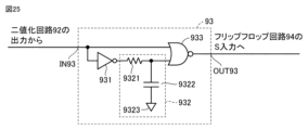
- FIG. 25 is a diagram showing an example of the configuration of the edge detection circuit 93.
- Edge detection circuit 93 detects a rising edge or a falling edge of the output signal of binarization circuit 92 and outputs a detection result. Whether a rising edge or a falling edge is detected can be changed depending on the polarity of the binarization circuit 92 or the polarity detected by the flip-flop circuit 94. A suitable edge is selected.
- the edge detection circuit 93 includes an inversion circuit (inverter) 931, a delay circuit 932, and a NOR circuit 933.
- the delay circuit 932 includes, for example, a resistive element 9321 and a capacitive element 9322.
- Input node IN93 of edge detection circuit 93 is connected to a first input terminal of NOR circuit 933, and also connected to a second input terminal of NOR circuit 933 via inverting circuit 931 and delay circuit 932 in this order.
- Resistance element 9321 of delay circuit 932 is connected between the output terminal of inversion circuit 931 and the second input terminal of NOR circuit 933.
- Capacitive element 9322 of delay circuit 932 is connected between the second input terminal of NOR circuit 933 and reference node 9323 to which reference potential Vref is applied.
- An input node IN93 of the edge detection circuit 93 is connected to the output of the binarization circuit 92.
- the output terminal of NOR circuit 933 is connected to the S input node of flip-flop circuit 94 via output node OUT93.
- FIG. 26 is a diagram showing an example of the configuration of the flip-flop circuit 94.
- Flip-flop circuit 94 includes two NOR circuits 941 and 942.
- a first input terminal of the NOR circuit 941 is connected as a set terminal S to an output node OUT93 of the edge detection circuit 93.
- a second input terminal of NOR circuit 941 is connected to an output terminal of NOR circuit 942.
- An output terminal of NOR circuit 941 is connected to a first input terminal of NOR circuit 942.
- a second input terminal of the NOR circuit 942 is connected to the output of the inversion circuit 95 as a reset terminal R.
- the output terminal of the NOR circuit 942 is connected to the input of the comparison circuit 4 as the output terminal Q of the flip-flop circuit 94.
- the flip-flop circuit 94 is activated by inputting the signal detected by the edge detection circuit 93 to the set terminal S, and by inputting the control signal inverted by the inverting circuit 95 to the reset terminal R. becomes inactive.
- FIG. 27 shows an example of the configuration of the inversion circuit 95.
- Inversion circuit 95 includes a NOT circuit 951.
- the inverting circuit 95 inverts the polarity of the control signal input from the control input terminal 7 and outputs the inverted control signal to the reset terminal R of the flip-flop circuit 94. As a result, the state held by the flip-flop circuit 94 is reset.
- FIG. 28 is a timing diagram for explaining an example of the operation of the power semiconductor drive circuit 2000 according to the second embodiment.
- FIG. 28 shows a timing diagram when the collector current Ic is relatively small during the turn-on operation of the power semiconductor element 8. From the top of FIG. 28, the control signal input to the control input terminal 7, the limited voltage VL output from the voltage limiting circuit 1, and the first variable voltage V1 output from the first variable voltage generation circuit 2 are shown in order from the top of FIG.
- the waveforms of the output of the mirror voltage detection circuit 9, the output of the determination result of the comparison circuit 4, the collector current Ic of the power semiconductor element 8, and the collector-emitter voltage Vce are shown.
- the case of the present embodiment is shown by a solid line
- the case of the comparative example is shown by a broken line.
- the comparative example shows a case of a constant voltage drive type or constant current drive type drive circuit that does not control the gate voltage Vg of the power semiconductor element 8 separately in a plurality of time regions.
- the power semiconductor element drive circuit 2000 controls the power semiconductor element 8 when the collector current Ic is relatively small and when the collector current Ic is relatively large. They are characterized by different methods of controlling collector current Ic and collector-emitter voltage Vce.
- the drive circuit 2000 of the second embodiment differences from the operation of the drive circuit 1000 of the first embodiment shown in FIG. 13 when the collector current is relatively small will be explained.
- the voltage limiting circuit 1 and the first changing voltage generating circuit 2 starts operating.
- the voltage change in the gate voltage Vg in the first region RG1 near time t0 is controlled by the voltage limiting circuit 1.
- the voltage limiting circuit 1 rapidly increases the gate voltage Vg in the first region RG1 with the first slope SL1 to approximately the threshold voltage Vth (corresponding to the limiting voltage VL). let This makes it possible to shorten dead time and reduce loss.
- the operation of drive circuit 2000 from time t0 to time t2 is almost the same as the operation of drive circuit 1000 of the first embodiment shown in FIG. 13. That is, the output composite voltage VL+V1 of the voltage limiting circuit 1 and the first variable voltage generation circuit 2, the output voltage V2 of the second variable voltage generation circuit 3, the output voltage V3 of the adder circuit 5, the collector current Ic, and the collector-emitter
- the waveform of the voltage Vce is the same as that of the drive circuit 1000 of the first embodiment shown in FIG.
- the flip-flop circuit 94 is in an inactive state until time t2 because the gate voltage Vg has not reached the mirror voltage Vm. Therefore, the output of mirror voltage detection circuit 9 is also at low (L) level.
- gate voltage Vg reaches mirror voltage Vm.
- the mirror voltage detection circuit 9 operates, and the differentiating circuit 91, the binarization circuit 92, and the edge detection circuit 93 detect the timing when the gate voltage Vg reaches the mirror voltage. Since a delay time occurs in the timing detection by the differentiator circuit 91, the binarization circuit 92, and the edge detection circuit 93, the set signal of the flip-flop circuit 94 changes from low to high at time t3, which is a certain period of time after time t2. do.
- the delay time that occurs in timing detection by the differentiator circuit 91, the binarization circuit 92, and the edge detection circuit 93 can be arbitrarily designed by the designer as a design parameter. Therefore, the designer can also arbitrarily design the interval from the timing when the gate voltage Vg reaches the mirror voltage Vm to the next operation, which is the timing when the comparison circuit 4 adjusts the rate of change of the gate voltage Vg.
- the output of the mirror voltage detection circuit 9 changes from low to high and maintains that state. Furthermore, when the output of the mirror voltage detection circuit 9 changes from low to high at time t3, the determination result of the comparison circuit 4 also changes from low to high.
- the determination result of the comparison circuit 4 becomes high, a current is injected into the gate terminal of the power semiconductor element 8, so that the gate voltage Vg rapidly increases at the fourth slope SL4. That is, in the example of FIG. 28, the second region RG2 directly transitions to the fourth region RG4 without passing through the third region RG3.
- the rate of change dVce/dt of the collector-emitter voltage Vce can be increased, so switching loss can be reduced.
- the gate voltage Vg controlled by the drive circuit of the comparative example is still in the mirror period, and loss due to switching occurs during the mirror period. Furthermore, in the case of the drive circuit 1000 of the first embodiment shown in FIG. , the timing at which the output of the comparison circuit 4 switches from low to high is determined. Therefore, depending on the setting of the comparison voltage, the timing at which the output of the comparison circuit 4 switches from low to high is delayed compared to the case of the drive circuit 2000 of the second embodiment.
- the mirror voltage detection circuit 9 detects the timing when the gate voltage Vg reaches the mirror voltage Vm.
- the comparison circuit 4 can be operated according to the detection result.
- the drive circuit 2000 of the second embodiment can have smaller loss than the drive circuit 1000 of the first embodiment.
- the set signal of the flip-flop circuit 94 changes to high at time t3, and then falls from high to low at time t4 in accordance with the operation of the edge detection circuit 93.
- the period during which the edge detection circuit 93 maintains a high level can be arbitrarily designed by a designer. Therefore, the period during which the edge detection circuit 93 maintains a high level can be arbitrarily set depending on the length of time during which the flip-flop circuit 94 can operate and the frequency at which the power semiconductor element 8 is operated.
- the reset signal of the flip-flop circuit 94 changes to high level.
- the state held by the flip-flop circuit 94 is reset. That is, the output of the mirror voltage detection circuit 9 and the determination result of the comparison circuit 4 both change from high to low. This completes the injection of current into the gate terminal of the power semiconductor element 8.
- FIG. 29 is a flowchart showing a control procedure when the power semiconductor element 8 is turned on by the drive circuit 2000 of the second embodiment.
- step ST110 of FIG. 29 the drive circuit 2000, in response to the turn-on command of the power semiconductor element 8, reaches the limit voltage VL corresponding to the threshold voltage Vth of the power semiconductor element 8 in the first time domain RG1.
- the gate voltage Vg of the power semiconductor element 8 is increased by the first slope SL1.
- the drive circuit 2000 changes the gate voltage Vg from the limit voltage VL with a second slope SL2 that is gentler than the first slope SL1 in a second time domain RG2 following the first time domain RG1. increase.
- step ST125 the drive circuit 2000 increases the gate voltage from the mirror voltage by a fourth slope SL4 that is steeper than the third slope SL3. Eventually, the gate voltage Vg increases to the power supply voltage supplied to the drive circuit 2000.
- step ST125 if the mirror voltage detection circuit 9 does not detect that the gate voltage Vg has reached the mirror voltage Vm after the first period has elapsed since receiving the turn-on command (NO in step ST125), The process proceeds to step ST130.
- step ST130 the drive circuit 2000 sets a third slope that is gentler than the first slope SL1 but steeper than the second slope SL2 in the third time domain RG3 following the second time domain RG2.
- the gate voltage Vg is increased to the mirror voltage Vm.
- the gate voltage Vg when the power semiconductor element 8 is turned on is basically the same as the drive circuit 1000 of the first embodiment.
- Control is divided into four time regions from a first region RG1 to a fourth region RG4.
- the gate voltage Vg is controlled by the voltage limiting circuit 1, and thereby rapidly increases to about the threshold voltage at the first slope SL1. This can shorten dead time and reduce loss.
- the gate voltage Vg is controlled by the first variable voltage generation circuit 2.
- the gate voltage Vg reaches the mirror voltage in this second region RG2. Since the rate of change of the voltage generated by the first variable voltage generation circuit 2 (corresponding to the second slope SL2) is smaller than the rate of change of the voltage generated by the second variable voltage generation circuit 3, recovery is possible.
- the rate of change dVce/dt of the collector-emitter voltage Vce due to current can be reduced, and as a result, EMI can be reduced.
- the next control in the third region RG3 is executed when the collector current Ic flowing through the power semiconductor element 8 is relatively large.
- the gate voltage Vg reaches the mirror voltage halfway through the third region RG3.
- the second variable voltage generation circuit 3 is used to control the gate voltage Vg to increase at the third slope SL3, which is larger than the second slope SL2. be done.
- the rate of change dIc/dt of the collector current Ic can be increased, thereby suppressing an increase in loss.
- the next control in the fourth region RG4 is executed based on the mirror voltage detection circuit 9 detecting the timing at which the gate voltage Vg reaches the mirror voltage Vm.
- the comparator circuit 4 By operating the comparator circuit 4 in response to detecting the timing at which the mirror voltage Vm is reached, the rate of change dVce/dt of the collector-emitter voltage Vce can be increased, and switching loss can be reduced. Since the comparison circuit 4 operates based on the detection result of the mirror voltage detection circuit 9, the switching loss is lower than in the case of the drive circuit 1000 of the first embodiment, in which the timing at which the comparison circuit 4 operates is delayed as the mirror voltage becomes smaller. can be reduced.
Abstract
電力用半導体素子(8)の駆動回路(1000)において、第1のゲート電圧制御回路(10)は、ターンオン指令に応答して第1の時間領域(RG1)、第2の時間領域(RG2)、および第3の時間領域(RG3)の順でそれぞれ異なる態様で電力用半導体素子(8)のゲート電圧(Vg)を制御することによって、ゲート電圧(Vg)をミラー電圧(Vm)に到達させる。ゲート電圧(Vg)は、電力用半導体素子(8)を流れる主電流の大きさに応じて、第2の時間領域(RG2)または第3の時間領域(RG3)においてミラー電圧(Vm)に到達する。第2のゲート電圧制御回路(4)は、ミラー電圧(Vm)以上のゲート電圧(Vg)を制御する。
Description
本開示は、電力用半導体素子の駆動回路および駆動方法ならびにパワーモジュールに関する。
大電力を制御する電力用半導体素子は、たとえば、直流および交流から周波数の異なる交流を発生させる電源回路、および電源回路を有する電力変換装置などに使用される。電力用半導体素子がインバータなどの電力変換装置に使用される場合には、省エネルギーおよび温室効果ガスの削減の観点から電力消費を抑えることが重要である。
特表2008-519529号公報(特許文献1)は、電力用半導体素子のスイッチングを制御することにより、電力用半導体素子で消費されるエネルギーを低減する方法を開示する。
具体的にこの文献は、「パワートランジスタスイッチをドライブする方法であって、ドライブ入力信号を受信する段階と、ドライブ入力信号を変換ドライブ入力信号に変換する段階と、変換ドライブ入力信号をスイッチの制御電極に与えて、スイッチをオンにする段階とを含み、変換ドライブ入力信号は、時間に関する3つの領域を有し、各々はスロープを有し、第1領域は、スイッチのミラープラトー(Miller Plateau)までの第1スロープがある時間であり、第2領域は、第1スロープに比べて小さいスロープより成る第2スロープがある時間であり、第3領域は、第2スロープよりも大きい第3スロープがある時間であり、それによって、制御電極電圧はミラープラトー電圧に急速に達し、次に、スイッチのしきい値電圧に低速で達し、次に、スイッチがほぼ完全にオンになると、制御電極電圧は急速に増大する。スイッチ遅延時間は、トランジスタ制御電極プリチャージ電圧を調整することによって、ほぼ一定に維持される」方法を開示する(特表2008-519529号公報の要約を参照)。
上記の特表2008-519529号公報(特許文献1)に開示された電力用半導体素子の制御方法によれば、スイッチング時の電流変化率(dI/dt)を低下させることによりEMI(電磁妨害)を低下させることができる。しかしながら、電力用半導体素子に流れる電流Iが大きい場合に電流変化率が小さくなるように制御すると、スイッチング時間が増えるためにかえってスイッチング損失が大きくなるという問題がある。上記の特許文献はこの点について考慮されていない。
本開示は、上記の問題点を考慮してなされたものであり、その目的の一つは、電力用半導体素子に流れる電流が比較的大きい場合でもスイッチング損失を抑制することが可能な電力用半導体素子の駆動回路を提供することである。
一実施形態の電力用半導体素子の駆動回路は、第1のゲート電圧制御回路と、第2のゲート電圧制御回路とを備える。第1のゲート電圧制御回路は、電力用半導体素子のターンオン指令に応答して第1の時間領域、第2の時間領域、および第3の時間領域の順でそれぞれ異なる態様で電力用半導体素子のゲート電圧を制御することによって、ゲート電圧をミラー電圧に到達させる。ゲート電圧は、電力用半導体素子を流れる主電流の大きさに応じて、第2の時間領域または第3の時間領域においてミラー電圧に到達する。第2のゲート電圧制御回路は、ミラー電圧以上のゲート電圧を制御する。
上記の実施形態によれば、駆動回路は、電力用半導体素子のターンオン指令に応答して第1の時間領域、第2の時間領域、および第3の時間領域の順でそれぞれ異なる態様で電力用半導体素子のゲート電圧を制御することによって、ゲート電圧をミラー電圧に到達させる。これにより、電力用半導体素子に流れる電流が比較的大きい場合でもスイッチング損失を抑制できる。
以下、各実施の形態について図面を参照して詳しく説明する。なお、同一または相当する部分には同一の参照符号を付して、その説明を繰り返さない。
実施の形態1.
[電力用半導体素子の駆動回路の構成]
図1は、実施の形態1による電力用半導体素子の駆動回路1000の構成を表すブロック図である。駆動回路1000は、制御入力端子7に入力される制御信号に従って、電力用半導体素子8のスイッチングを制御するためのゲート電圧Vgを生成する。より詳細には、駆動回路1000は、電力用半導体素子8のターンオン動作時のゲート電圧Vgの電圧変化を、順に第1の時間領域(図13、図14のRG1)から第4の時間領域(図13、図14のRG4)までの4つの時間領域で制御する。以下の説明では、第1~第4の時間領域を単に第1~第4領域とも記載する。
[電力用半導体素子の駆動回路の構成]
図1は、実施の形態1による電力用半導体素子の駆動回路1000の構成を表すブロック図である。駆動回路1000は、制御入力端子7に入力される制御信号に従って、電力用半導体素子8のスイッチングを制御するためのゲート電圧Vgを生成する。より詳細には、駆動回路1000は、電力用半導体素子8のターンオン動作時のゲート電圧Vgの電圧変化を、順に第1の時間領域(図13、図14のRG1)から第4の時間領域(図13、図14のRG4)までの4つの時間領域で制御する。以下の説明では、第1~第4の時間領域を単に第1~第4領域とも記載する。
図1に示すように、駆動回路1000は、電圧制限回路1と、第1の変化電圧生成回路2と、第2の変化電圧生成回路3と、比較回路4と、加算回路5と、バッファ回路6とを備える。ここで、電圧制限回路1、第1の変化電圧生成回路2、第2の変化電圧生成回路3、加算回路5、およびバッファ回路6をまとめて第1のゲート電圧制御回路10と称する。第1のゲート電圧制御回路10は、ターオン指令に応答して第1の時間領域RG1、第2の時間領域RG2、および第3の時間領域RG3の順でそれぞれ異なる態様で電力用半導体素子8のゲート電圧Vgを制御することによって、ゲート電圧Vgをミラー電圧Vmに到達させる。ゲート電圧Vgは、第2領域RG2または第3領域RG3においてミラー電圧Vmに到達する。第2のゲート電圧制御回路としての比較回路4は、ミラー期間の後のゲート電圧Vgを制御する。以下、各回路の機能を簡単に記載する。
電圧制限回路1は、第1領域RG1でのゲート電圧Vgの電圧変化を制御する。具体的に電圧制限回路1は、ターンオン指令に応答して制限電圧VL(第1の電圧とも称する)を出力することにより、第1の傾斜(図13、図14のSL1)で制限電圧VLまでゲート電圧Vgを急激に増加させる。すなわち、電圧制限回路1は、電力用半導体素子8の立ち上がり時にゲート電圧Vgを制限電圧VLに制限する。好ましくは、制限電圧VLは、電力用半導体素子8のしきい値電圧Vthに対応しており、概ねしきい値電圧Vth程度の値を有している。
第1の変化電圧生成回路2は、第2領域RG2でのゲート電圧Vgの電圧変化を制御する。具体的に第1の変化電圧生成回路2は、第1の傾斜SL1よりも緩やかな第2の傾斜(図13、図14のSL2)で増加する第1の変化電圧V1を生成する。第1の変化電圧生成回路2は、生成した第1の変化電圧V1を電力用半導体素子8のゲートにバッファ回路6を介して供給することにより、ゲート電圧Vgを制限電圧VLから第2の傾斜SL2で増加させる。
第2の変化電圧生成回路3は、第3領域RG3でのゲート電圧Vgの電圧変化を制御する。具体的に第2の変化電圧生成回路3は、第1の変化電圧生成回路2から出力される第1の変化電圧V1よりも急峻に変化する第2の変化電圧V2を生成する。これにより、ターンオン指令を受けてから第1の期間(図13の時刻t0からt3まで、図14の時刻t0からt2まで)が経過した時点でゲート電圧Vgがミラー電圧に達していない場合に、上記の第1の傾斜SL1よりも緩やかであるが、第2の傾斜SL2よりも急な第3の傾斜SL3で、ゲート電圧Vgはミラー電圧まで増加する。
比較回路4は、第4領域RG4でのゲート電圧Vgの電圧変化を制御する。具体的に比較回路4は、ターンオン指令を受けてから第2の期間(図13、図14の時刻t0からt4まで)が経過した時点から、上記の第3の傾斜SL3よりも急な第4の傾斜SL4でゲート電圧Vgをミラー電圧から増加させる。最終的に、ゲート電圧Vgは、駆動回路1000に供給される電源電圧に到達する。
加算回路5は、ターンオン指令を受けてから上記の第1の期間が経過するまでは、制限電圧VLに第1の変化電圧V1が加算された電圧を出力する。加算回路5は、ターンオン指令を受けてから上記の第1の期間が経過した時点から、電圧制限回路1の出力電流と第1の変化電圧生成回路2の出力電流と第2の変化電圧生成回路3の出力電流とを加算した電流を出力し、上記の制限電圧VL、第1の変化電圧V1、および第2の変化電圧V2に基づく第3の変化電圧V3を出力する。バッファ回路6は、加算回路5の出力電圧を電力用半導体素子8のゲートに伝達することにより、電力用半導体素子8のゲート電圧Vgを生成する。
上記の4つの時間領域についてまとめると、第1領域RG1は、ターンオン指令を受けた直後のゲート電圧Vgの立ち上がり時に対応する。第2領域RG2は、ゲート電圧Vgが立ち上がった後、上記の第1の期間が経過するまでの時間領域である。第3領域RG3は、上記の第1の期間が経過してから第2の期間が経過するまでの時間領域である。第4領域RG4は、上記の第2の期間が経過してからゲート電圧Vgが駆動回路1000の電源電圧に到達するまでの時間領域である。
図2は、電圧制限回路1の構成の一例を示す図である。電圧制限回路1は、一例として、ツェナーダイオード11で構成される。
図2に示すように、電圧制限回路1の入力ノード(Node:節点)IN1は、電力用半導体素子8を外部から制御するための制御入力端子7に接続される。電圧制限回路1の出力ノードOUT1は、加算回路5に接続される。電圧制限回路1の内部において、ツェナーダイオード11のカソードは、入力ノードIN1に接続され、ツェナーダイオード11のアノードは、出力ノードOUT1に接続される。
上記の電圧制限回路1の構成によれば、電圧制限回路1は、ターンオン動作の指令として制御入力端子7に入力される制御信号がロウからハイに変化したときに、出力ノードOUT1の電圧変化を制限する。具体的に、電圧制限回路1の出力ノードOUT1の電圧は、電圧制限回路1の入力ノードIN1の電圧がツェナーダイオード11のツェナー電圧(以下、制限電圧VLとも称する)に達するまで変化せず、その後はツェナー電圧に制限される。これにより、電圧制限回路1は、急峻に変化する電圧を生成して、第1領域RG1でのゲート電圧Vgの電圧変化を制御する。
図3および図4は、第1の変化電圧生成回路2の構成の一例を示す図である。第1の変化電圧生成回路2の入力ノードIN2は制御入力端子7に接続され、第1の変化電圧生成回路2の出力ノードOUT2は電圧制限回路1の出力ノードOUT1に接続される。第1の変化電圧生成回路2は、ターンオン動作の指令として制御入力端子7に入力される制御信号がロウからハイに変化したときに、電圧制限回路1で制限された電圧値である制限電圧VLを基準にして、第1の時間的変化率dV1/dtで比較的緩やかに増加する第1の変化電圧V1を生成して、加算回路5に出力する。これにより、第1の変化電圧生成回路2は、ゲート電圧Vgがミラー電圧に達する前の第2領域RG2でのゲート電圧Vgの時間変化(第1の傾斜SL1に対応する)を制御する。
具体的に図3の構成例では、第1の変化電圧生成回路2は、抵抗素子21と容量素子22とを含む一次遅れ回路として構成される。抵抗素子21は、入力ノードIN2と出力ノードOUT2との間に接続される。容量素子22は、出力ノードOUT2と基準電位Vrefを与える基準ノード23との間に接続される。この構成によれば、抵抗素子21の抵抗値Rと容量素子22の容量値Cとで決まる時定数CRに従って、出力ノードOUT2の電圧は、制限電圧VLから比較的緩やかにほぼ一定の時間増加率で増加する。
図4の構成例では、第1の変化電圧生成回路2は、定電流源24と容量素子22とを含む。定電流源24は、電源電圧が与えられる電源ノード25と出力ノードOUT2との間に接続される。容量素子22は、出力ノードOUT2と基準ノード23との間に接続される。定電流源24は、ターンオン動作の指令として制御入力端子7に入力される制御信号がロウからハイに変化したときに定電流を容量素子22に流し始める。これにより、容量素子22の電圧は、制限電圧VLから一定の時間的変化率で増加する。
図5および図6は、第2の変化電圧生成回路3の構成の一例を示す図である。第2の変化電圧生成回路3の入力ノードIN3は制御入力端子7に接続され、第2の変化電圧生成回路3の出力ノードOUT3は比較回路4および加算回路5に接続される。第2の変化電圧生成回路3は、ターンオン動作の指令として制御入力端子7に入力される制御信号がロウからハイに変化したときに、駆動回路1000の基準電位Vrefを基準にして、第2の時間的変化率dV2/dtで比較的緩やかに増加する第2の変化電圧V2を生成して出力する。ここで、第2の変化率dV2/dtは、前述の第1の変化率dV1/dtよりも大きい。ゲート電圧Vgがミラー電圧に達する前の第3領域RG3でのゲート電圧Vgの時間変化(第3の傾斜SL3に対応する)は、第2の変化電圧生成回路3から出力される第2の変化電圧V2の時間変化率dV2/dtに基づいている。
具体的に図5の構成例では、図3の場合と同様に、第2の変化電圧生成回路3は、抵抗素子31と容量素子32とを含む一次遅れ回路として構成される。抵抗素子31は、入力ノードIN3と出力ノードOUT3との間に接続される。容量素子33は、出力ノードOUT3と基準電位Vrefを与える基準ノード33との間に接続される。この構成によれば、抵抗素子31の抵抗値Rと容量素子33の容量値Cとで決まる時定数CRに従って、出力ノードOUT3の電圧は、基準電位Vrefからほぼ一定の増加率で比較的緩やかに増加する。
図6の構成例では、図4の場合と同様に、第2の変化電圧生成回路3は、定電流源34と容量素子32とを含む。定電流源34は、電源電圧が与えられる電源ノード35と出力ノードOUT3との間に接続される。容量素子33は、出力ノードOUT3と基準ノード33との間に接続される。定電流源34は、ターンオン動作の指令として制御入力端子7に入力される制御信号がロウからハイに変化したときに定電流を容量素子33に流し始める。これにより、容量素子33の電圧は、基準電位Vrefから一定の時間増加率で増加する。
図7は、比較回路4の構成の一例を示す図である。図7に示すように、比較回路4は、比較器41と比較電圧源42とを含む。比較回路4の入力ノードIN4は第2の変化電圧生成回路3の出力ノードOUT3に接続され、比較回路4の出力ノードOUT4は電力用半導体素子8のゲート端子に接続される。比較回路4の内部において、比較器41の非反転入力端子は入力ノードIN4に接続され、比較器41の反転入力端子は比較電圧源42に接続され、比較器41の出力端子は出力ノードOUT4に接続される。
上記の比較回路4の構成によれば、比較回路4は、第2の変化電圧生成回路3から出力される第2の変化電圧V2が比較電圧源42の電圧値(すなわち、比較電圧VC)に達するまではロウレベル(すなわち、駆動回路1000の基準電位Vref)を出力し、その後、ハイレベル(すなわわち、駆動回路1000の電源電圧)を出力する。これにより、比較回路4は、第4の傾斜SL4で急峻に増加する電圧を生成し、ゲート電圧Vgがミラー電圧以上になる第4領域におけるゲート電圧Vgの変化を制御する。なお、比較回路4は、第1の変化電圧生成回路2から出力される第1の変化電圧V1と比較電圧VCとを比較するように構成されていてもよい。比較電圧VCの値は、第1の変化電圧V1の電圧変化率dV1/dtに応じて調整される。
図8は、加算回路5の構成の一例を示す図である。図8に示すように、加算回路5は、ダイオード51を含む。加算回路5の入力ノードIN5Aは、電圧制限回路1の出力ノードOUT1および第1の変化電圧生成回路2の出力ノードOUT2に接続される。加算回路5の入力ノードIN5Bは、第2の変化電圧生成回路3の出力ノードOUT3に接続される。加算回路5の出力ノードOUT5Bは、バッファ回路6の入力ノードIN6に接続される。加算回路5の内部において、入力ノードIN5Aと出力ノードOUT5とは配線によって直接接続される。ダイオード51は、入力ノードIN5Bと出力ノードOUT5との間に、入力ノードIN5Bから出力ノードOUT5への方向が順方向となるように接続される。
上記の加算回路5の構成によれば、第2の変化電圧生成回路3から出力された第2の変化率で増加する第2の変化電圧V2が、電圧制限回路1から出力された制限電圧VLと第1の変化電圧生成回路2から出力された第1の変化率で増加する第1の変化電圧V1との合成電圧(VL+V1)に達するまでは、加算回路5は出力ノードOUT5から合成電圧(VL+V1)を出力する。その後、加算回路5は、電圧制限回路1の出力電流と第1の変化電圧生成回路2の出力電流と第2の変化電圧生成回路3の出力電流とを加算した電流を出力し、合成電圧(VL+V1)と第2の変化電圧V2とに基づく第3の変化電圧V3を出力する。第3の変化電圧V3の値は、ダイオード51の特性および寄生容量などによって決まる。第3の変化電圧V3の時間変化率dV3/dtは、第1の変化電圧V1の時間変化率dV1/dtよりも大きくなる。前述の第1の期間は、第2の変化電圧V2が制限電圧VLと第1の変化電圧V1との和に等しくなるまでの期間に対応する。
図9、図10、および図11は、バッファ回路6の構成の一例を示す図である。バッファ回路6は、入力ノードIN6を介して入力された加算回路5の出力電圧を、出力ノードOUT6を介して電力用半導体素子8のゲートに伝達することにより、電力用半導体素子8のゲート電圧Vgを生成する。
具体的に図9の構成例では、バッファ回路6は、NPN型バイポーラトランジスタ61のエミッタフォロアによって構成される。エミッタフォロアの電圧増幅率は1である。より詳細には、バイポーラトランジスタ61のコレクタは電源電圧が与えられる電源ノード62に接続され、バイポーラトランジスタ61のエミッタは出力ノードOUT6に接続され、バイポーラトランジスタ61のベースは入力ノードIN6に接続される。
図10の構成例では、バッファ回路6は、NPN型のバイポーラトランジスタ61とPNP型のバイポーラトランジスタ63のプッシュプル型のエミッタフォロアで構成される。エミッタフォロアの電圧増幅率は1である。より詳細には、バイポーラトランジスタ61のコレクタは電源電位が与えられる電源ノード62に接続され、バイポーラトランジスタ63のコレクタは基準電位Vrefが与えられる基準ノード64に接続される。バイポーラトランジスタ61,63のエミッタは、出力ノードOUT6に接続される。バイポーラトランジスタ61,63のベースは、入力ノードIN6に接続される。
図11の構成例では、バッファ回路6は、オペアンプ65を利用したユニティ・ゲイン・バッファによって構成される。より詳細には、オペアンプ65の出力端子は、出力ノードOUT6に接続されるとともに、オペアンプ65の反転入力端子に接続される。オペアンプ65の非反転入力端子は入力ノードIN6に接続される。
図12は、電力用半導体素子8の構成の一例を示す図である。図12に示す例では、電力用半導体素子8は、IGBT(Insulated Gate Bipolar Transistor)81とフリーホイールダイオード82とで構成される。IGBTに代えて、FET(Field Effect Transistor)であってもよいし、バイポーラトランジスタであってもよく、半導体素子の種類は特に限定されない。本開示では、電力用半導体素子8の制御電極をゲートとも称し、制御電極の電圧をゲート電圧とも称する。
[電力用半導体素子の駆動回路の動作]
次に、電力用半導体素子8のターンオン時における実施の形態1の駆動回路1000の動作について説明する。以下では、電力用半導体素子8の主電流であるコレクタ電流Icが比較的小さい場合の動作について図13を参照して説明し、電力用半導体素子8のコレクタ電流Icが比較的大きい場合の動作について図14を参照して説明する。実施の形態1による電力用半導体素子の駆動回路1000は、コレクタ電流Icが小さい場合と大きい場合とで、電力用半導体素子8のゲート電圧Vgの制御方法が異なる点を特徴としている。
次に、電力用半導体素子8のターンオン時における実施の形態1の駆動回路1000の動作について説明する。以下では、電力用半導体素子8の主電流であるコレクタ電流Icが比較的小さい場合の動作について図13を参照して説明し、電力用半導体素子8のコレクタ電流Icが比較的大きい場合の動作について図14を参照して説明する。実施の形態1による電力用半導体素子の駆動回路1000は、コレクタ電流Icが小さい場合と大きい場合とで、電力用半導体素子8のゲート電圧Vgの制御方法が異なる点を特徴としている。
図13は、実施の形態1による電力用半導体素子の駆動回路1000の第1の動作例を説明するためのタイミング図である。図13では、電力用半導体素子8のターンオン動作時においてコレクタ電流Icが比較的小さい場合のタイミング図が示されている。図13の上から順に、制御入力端子7に入力される制御信号、電圧制限回路1から出力される制限電圧VLと第1の変化電圧生成回路2から出力される第1の変化電圧V1との和(VL+V1)、第2の変化電圧生成回路3から出力される第2の変化電圧V2、加算回路5の出力電圧V3、比較回路4の判定結果、電力用半導体素子8のゲート電圧Vg、コレクタ電流Ic、およびコレクタ・エミッタ間電圧Vceの各波形が示されている。ゲート電圧Vg、コレクタ電流Ic、およびコレクタ・エミッタ間電圧Vceの波形では、本実施形態の場合を実線で示し、比較例の場合を破線で示す。比較例は、電力用半導体素子8のゲート電圧Vgを複数の時間領域に別けて制御しない定電圧駆動型または定電流駆動型の駆動回路の場合を示している。
以下、時系列順に説明する。まず、図13の時刻t0における駆動回路1000の動作を説明する。
時刻t0において、ターンオン動作の指令として、制御入力端子7に入力される制御信号がロウからハイに変化すると、電圧制限回路1と第1の変化電圧生成回路2と第2の変化電圧生成回路3とが動作を開始する。時刻t0近傍の第1領域RG1でのゲート電圧Vgの電圧変化は、電圧制限回路1によって制御される。
具体的に、電圧制限回路1の出力電圧V1は、制限電圧VLまで第1の傾斜SL1で急激に上昇する。ここで、電圧制限回路1の制限電圧VLは、電力用半導体素子8のしきい値電圧Vth程度に設定されている。この結果、ゲート電圧Vgが電力用半導体素子8のしきい値電圧Vthに達することにより、電力用半導体素子8にコレクタ電流Icが流れ始める。一方、比較例の駆動回路の場合には、ゲート電圧Vgが上昇し始めるが、しきい値電圧Vthに到達するまでに時間がかかるので、コレクタ電流Icはすぐには上昇しない。このように、実施の形態1の駆動回路1000によれば、比較例の駆動回路と比較して、第1領域RG1でのゲート電圧Vgを第1の傾斜SL1でしきい値電圧程度まで急峻に上昇させることにより、デッドタイムを短縮し、損失を小さくできる。
時刻t0において、さらに、第1の変化電圧生成回路2の出力電圧V1は、電圧制限回路1の制限電圧VLを基準にして第1の時間的変化率dV1/dtで上昇し始める。また、第2の変化電圧生成回路3の出力電圧V2は、駆動回路1000の基準電位Vrefを基準に、第2の時間的変化率dV2/dtで上昇し始める。ここで、実施の形態1の駆動回路1000では、第1の変化電圧生成回路2で生成する第1の変化電圧V1の変化率dV1/dtよりも、第2の変化電圧生成回路3で生成する第2の変化電圧V2の変化率dV2/dtの方が大きい。
時刻t0近傍において、第2の変化電圧生成回路3から出力される第2の変化電圧V2よりも電圧制限回路1および第1の変化電圧生成回路2の出力される制限電圧VLと第1の変化電圧V1との和のほうが大きいため、加算回路5の出力電圧V3は、制限電圧VLと第1の変化電圧V1との和に等しくなる。比較回路4の判定結果は、比較電圧源42の出力電圧(すなわち、比較電圧VC)よりも第2の変化電圧生成回路3の出力電圧V2の方が小さいため、ロウ(L)レベルである。
以下、時刻t0近傍における電力用半導体素子8のゲート電圧Vg、コレクタ電流Ic、コレクタ・エミッタ間電圧Vceの変化を、本実施形態の場合と比較例の場合とで対比して説明する。本実施形態の場合のゲート電圧Vgは、ターンオン動作の指令である制御信号がロウからハイに変化すると、電圧制限回路1の動作によって、第1領域RG1における第1の傾斜SL1で急峻に増加してしきい値電圧Vthに達する。一方、比較例の駆動回路の場合、ターンオン動作の指令である制御信号がロウからハイに変化すると、緩やかに上昇し始めるが、すぐにはしきい値電圧Vthに達しない。
本実施形態の場合のコレクタ電流Icは、電圧制限回路1で設定された制限電圧VLに基づいてゲート電圧Vgがしきい値電圧Vthに達するために、すぐに流れ始める。比較例の場合のコレクタ電流Icは、ゲート電圧Vgがしきい値電圧Vthに達していないために0のまま変化しない。
電力用半導体素子8のコレクタ・エミッタ間電圧Vceは、コレクタ電流Icが流れ始めるため、その変化率dIc/dtに影響されて低下し始める。比較例の場合のコレクタ・エミッタ間電圧Vceは、コレクタ電流Icが流れていないために変化しない。
次に、図13の時刻t0からt1までの駆動回路1000の動作について説明する。電圧制限回路1は、制限電圧VLを出力し、第1の変化電圧生成回路2は第1の変化率dV1/dtで増加する第1の変化電圧V1を出力する。したがって、これらの電圧が加算された合成電圧(VL+V1)は、制限電圧VLを基準として、第1の変化率dV1/dtで上昇する。第2の変化電圧生成回路3の出力電圧V2は、駆動回路1000の基準電位Vrefを基準にして第2の変化率dV2/dtで上昇する。
加算回路5の出力電圧V3は、上記の第2の変化電圧V2よりも合成電圧(VL+V1)のほうが大きいため、制限電圧VLを基準として第1の変化率dV1/dtで増加する。比較回路4の判定結果は、比較電圧VCよりも第2の変化電圧生成回路3の出力電圧V2の方が小さいため、ロウのままである。
本実施形態の場合のゲート電圧Vgは、時刻t0の近傍の第1領域RG1においてしきい値電圧Vthまで第1の傾斜SL1で急激に上昇する。その後、ゲート電圧Vgは、第2領域RG2において、第1の変化電圧生成回路2の出力電圧の変化率dV1/dtに基づいて第2の傾斜SL2で比較的緩やかな変化率で上昇する。比較例の駆動回路の場合のゲート電圧Vgは、時刻t1で電力用半導体素子8のしきい値電圧Vthに達する。
本実施形態の場合において、電力用半導体素子8のコレクタ電流Icは、第2領域RG2において第2の傾斜SL2で変化するゲート電圧Vgに基づいた電流変化率で上昇する。比較例の駆動回路の場合のコレクタ電流Icは、時刻t1でゲート電圧Vgがしきい値電圧Vthに達するために流れ始める。
本実施形態の場合のコレクタ・エミッタ間電圧Vceは、コレクタ電流Icの変化率に影響されて低下する。比較例の駆動回路の場合のコレクタ・エミッタ間電圧Vceは、コレクタ電流Icが流れていない間は変化せず、時刻t1でコレクタ電流Icが流れ始めた後に低下し始める。
次に、図13の時刻t1からt2までの駆動回路1000の動作について説明する。電圧制限回路1および第1の変化電圧生成回路2の出力電圧V1と、第2の変化電圧生成回路3の出力電圧V2と、加算回路5の出力電圧V3と、比較回路4の出力は、時刻t0からt1までの場合と同様であるので説明を繰り返さない。
本実施形態の場合のゲート電圧Vgは、時刻t0から時刻t1までの場合と同様に、第2領域RG2において、第1の変化電圧生成回路2の出力電圧の電圧変化率dV1/dtに基づき、第2の傾斜で比較的緩やかに上昇し、時刻t2でミラー電圧に達する。比較例の駆動回路の場合のゲート電圧Vgは、時刻t1でしきい値電圧に達する。したがって、比較例の駆動回路の場合、時刻t1からコレクタ電流Icが流れ始める。
ここで、比較例の場合のゲート電圧Vgの変化率は、本実施形態の場合の第2領域RG2における第2の傾斜SL2に対応するゲート電圧Vgの変化率よりも大きい。このため、比較例の場合のコレクタ電流Icの変化率dIc/dtは、本実施形態の場合のコレクタ電流Icの変化率dIc/dtよりも大きい。結果として、本実施の形態の場合は、比較例の駆動回路の場合に比べて第2領域RG2での電力用半導体素子8のスイッチング損失が大きくなる。しかしながら、図13の場合は、コレクタ電流Icが比較的小さい場合であるので、この損失の影響は小さい。
電力用半導体素子8のコレクタ・エミッタ間電圧Vceの変化は、コレクタ電流Icの変化率dIc/dtの影響を受ける。したがって、比較例の駆動回路の場合の変化率dIc/dtのほうが本実施形態の場合よりも大きいので、比較例の駆動回路の場合のコレクタ・エミッタ間電圧Vceの変化率も、本実施形態の場合よりも大きい。
次に、図13の時刻t2からt3までの駆動回路1000の動作について説明する。電圧制限回路1および第1の変化電圧生成回路2の出力電圧V1と、第2の変化電圧生成回路3の出力電圧V2とは、時刻t0からt2までの場合と同様であるので説明を繰り返さない。
時刻t3に達するまでは時刻t0から時刻t2の場合と同様に、第2の変化電圧生成回路3の出力される第2の変化電圧V2よりも、電圧制限回路から出力される制限電圧VLと第1の変化電圧生成回路2から出力される第1の変化電圧V1との和(VL+V1)のほうが大きい。このため、加算回路5の出力電圧V3は、制限電圧VLと第1の変化電圧V1との和に等しい。時刻t3以降では、制限電圧Vと第1の変化電圧V1との和(VL+V1)よりも第2の変化電圧V2の方が大きくなるため、加算回路5の出力電圧V3は、制限電圧VLと第1の変化電圧V1と第2の変化電圧V2とに基づく値になり、その変化率はdV1/dtより大きい。また、加算回路5の出力電流は、電圧制限回路1の出力電流と第1の変化電圧生成回路2の出力電流と第2の変化電圧生成回路3の出力電流との和に等しい。ここで、第2領域RG2は、第1領域RG1において第1の傾斜SL1でゲート電圧Vgが急激に変化した後から、時刻t3までの期間(前述の第1の期間)である。
図13の場合、電力用半導体素子8のコレクタ電流Icが小さい第2領域RG2において、ゲート電圧Vgがミラー期間に達する。第2領域RG2は、リカバリ電流が流れてから回復する時間(図13では時刻t3まで)を含む。この第2領域RG2では、駆動回路1000は、第1の変化電圧生成回路2で生成された比較的緩やかな電圧変化率dV1/dtを有する第1の変化電圧V1に基づいてゲート電圧Vgを制御する点に特徴がある。
本実施の形態の場合の第2領域RG2でのゲート電圧Vgは、第1の変化電圧生成回路2で設定した電圧変化率dV1/dtに基づいて第2の傾斜SL2で変化するので、比較例の駆動回路の場合よりもゲート電圧Vgの変化率が小さく、リカバリ時のコレクタ電流Icの変化率dIc/dtも小さくなる。この結果、リカバリ電流によるコレクタ・エミッタ間電圧Vceの変化率dVce/dtも小さくなるため、EMIを低減できる。
なお、上記の説明では、本実施形態の場合の第2領域RG2におけるコレクタ電流Icの変化率dIc/dtを比較例の駆動回路の場合よりも小さいと仮定としている。しかしながら、第1の変化電圧生成回路2から出力される第1の変化電圧V1の変化率dV1/dtの設定次第では、比較例の駆動回路の場合よりも本実施形態の場合のコレクタ電流Icの変化率dIc/dtを大きくなる。その場合には比較例の場合よりも本実施形態の場合のほうがリカバリ電流によるEMIが大きくなるが、その一方で第2領域RG2でのスイッチング損失をより低減できるというメリットがある。
次に、図13の時刻t3からt4までの駆動回路1000の動作について説明する。時刻t3以降において、電圧制限回路1から出力される制限電圧VLと第1の変化電圧生成回路2から出力される第1の変化電圧V1との和よりも、第2の変化電圧生成回路3から出力される第2の変化電圧V2の方が大きくなる。このため、加算回路5の出力電圧V3は、時刻t3以降において制限電圧VLおよび第1の変化電圧V1だけでなく第2の変化電圧V2にも基づいて変化する。
第3領域RG3は、主として第2の変化電圧生成回路3の出力電圧V2に基づいてゲート電圧Vgを制御する期間である。しかし、ゲート電圧Vgは第2領域RG2の時刻t2でミラー期間に達しているため、第3領域RG3におけるゲート電圧Vgは一定である。比較例の駆動回路の場合も同様に、ゲート電圧Vgは時刻t2でミラー電圧に達しているため、第3領域RG3において一定である。
電力用半導体素子8のコレクタ電流Icは、時刻t3でリカバリ電流が回復しているため、時刻t3以降は一定である。比較例の駆動回路の場合もコレクタ電流Icは同様に時刻3以降において一定である。電力用半導体素子8のコレクタ・エミッタ間Vceは、バッファ回路6の駆動能力に応じた電圧変化率dVce/dtで低下する。比較例の駆動回路の場合も、コレクタ・エミッタ間電圧Vceは、駆動回路の駆動能力に応じた電圧変化率で低下する。
次に、図13の時刻t4から時刻t5までの駆動回路1000の動作について説明する。時刻t4において、比較回路4へ入力される第2の変化電圧生成回路3の出力電圧V2が、比較回路4の比較電圧VCに到達する。この結果、比較回路4の判定結果がロウからハイに変化する。比較回路4の判定結果がハイになると電力用半導体素子8のゲート端子に電流が注入されるため、ゲート電圧Vgは、第4の傾斜SL4で急激に上昇する。なお、時刻t0から時刻t4までが前述の第2の期間に対応する。
第4領域RG4は、比較回路4の出力電圧の変化に基づいて第4の傾斜SL4でゲート電圧Vgが増加する時間領域である。すなわち、ゲート電圧Vgのミラー期間の終了(時刻t4)から、ゲート電圧Vgが駆動回路1000の電源電圧に達する(時刻t5)までの期間である。一方、比較例の駆動回路のゲート電圧Vgは、時刻t5以降も時刻t6までミラー期間中であり、ミラー期間中はスイッチングによる損失が発生する。
このように、本実施形態の駆動回路1000によれば、比較回路4を用いて第4領域RG4でのゲート電圧Vgを制御し、ゲート電圧Vgを第4の傾斜SL4で急激に増加させる。これにより、コレクタ・エミッタ間電圧Vceの時間的変化率dVce/dtを大きくできるので、比較例の駆動回路の場合と比べて、第4領域RG4でのスイッチング損失を低減できる。また、実施の形態1の駆動回路1000では、第4領域RG4における第4の傾斜SL4のほうが第2領域RG2における第2の傾斜SL2よりも大きい点に特徴がある。
次に、図13の時刻t5以降の駆動回路1000の動作について説明する。本実施形態の駆動回路1000の場合、時刻t5でコレクタ電流Icおよびコレクタ・エミッタ間電圧Vceの変化は終了しているため、以降はターンオフ指令が入力されるまでこれらの状態は変わらない。
一方、比較例の駆動回路の場合、ゲート電圧Vgは、時刻t2でミラー電圧に達した後、ミラー期間の長さは駆動回路の出力電流の大きさに依存する。図13の場合には、時刻t6までミラー期間が継続する。時刻t3までの間にコレクタ・エミッタ間電圧Vceがある一定値まで下がると、その後、コレクタ・エミッタ間電圧Vceはミラー期間が終了する時刻t6まで緩やかに低下し続ける。そのため、時刻t3からt6までの期間は、スイッチング損失の増加の原因になる。
以上のように、実施の形態1の駆動回路1000によれば、電力用半導体素子8のターンオン時のゲート電圧Vgは、第1領域RG1から第4領域第4領域RG4までの4つの時間領域に分けて制御される。具体的に第1領域RG1では、ゲート電圧Vgは電圧制限回路1によって制御されることにより、第1の傾斜SL1で急激にしきい値電圧程度まで上昇する。これより、デッドタイムを短縮し、損失を小さくできる。
次の第2領域RG2では、ゲート電圧Vgは第1の変化電圧生成回路2によって制御される。電力用半導体素子8に流れるコレクタ電流Icが小さい場合、この第2領域RG2において、ゲート電圧Vgがミラー電圧に達する。第1の変化電圧生成回路2によって生成される電圧の変化率は、第2の変化電圧生成回路3によって生成される電圧の変化率よりも小さいので、リカバリ電流によるコレクタ・エミッタ間電圧Vceの変化率dVce/dtを小さくでき、結果としてEMIを低減できる。
その次の第3領域RG3では、ゲート電圧Vgは主として第2の変化電圧生成回路3によって制御される。電力用半導体素子8に流れるコレクタ電流Icが小さい場合、第2領域RG2においてゲート電圧Vgはミラー電圧に達しているので、第3領域RG3におけるゲート電圧Vgは一定である。
その次の第4領域RG4では、ゲート電圧Vgは比較回路4の出力電圧で制御される。この第4領域RG4でのゲート電圧Vgの変化率(第4の傾斜SL4に対応する)を、第1の変化電圧生成回路2で制御される第2領域RG2におけるゲート電圧Vgの電圧変化率(第2の傾斜SL2に対応する)よりも大きくする。この結果、コレクタ・エミッタ間電圧Vceの変化率dVce/dtを大きくできるので、スイッチング損失を低減できる。
図14は、実施の形態1による電力用半導体素子の駆動回路1000の第2の動作例を説明するためのタイミング図である。図14では、電力用半導体素子8のターンオン動作時においてコレクタ電流が比較的大きい場合のタイミング図が示されている。図14に示す各波形は、図13に示す各波形にそれぞれ対応している。図13の場合と同様に、ゲート電圧Vg、コレクタ電流Ic、およびコレクタ・エミッタ間電圧Vceの波形では、本実施形態の場合を実線で示し、比較例の場合を破線で示す。比較例は、電力用半導体素子8のゲート電圧Vgを複数の時間領域に別けて制御しない定電圧駆動型または定電流駆動型の駆動回路の場合を示している。
図14の時刻t0から時刻t1までの駆動回路1000の制御動作およびゲート電圧Vgの変化は、図13の場合と同様であるので説明を繰り返さない。
次に、図14の時刻t1からt2までの駆動回路1000の動作について説明する。電圧制限回路1から出力される制限電圧VLと、第1の変化電圧生成回路2から出力される第1の変化電圧V1と、第2の変化電圧生成回路3から出力される第2の変化電圧V2と、加算回路5の出力電圧V3と、比較回路4の出力は、時刻t0からt1までの場合と同様である。
本実施形態の場合のゲート電圧Vgは、時刻t0から時刻t1までの場合と同様に、第2領域RG2において、電圧制限回路1および第1の変化電圧生成回路2の出力電圧V1の電圧変化率dV1/dtに基づき、比較的緩やかな第2の傾斜SL2で増加する。図13のようにコレクタ電流Icが比較的小さい場合には、ミラー電圧も比較的小さいため、ゲート電圧Vgは時刻t2でミラー電圧Vmに達した。一方、図14のようにコレクタ電流Icが比較的大きい場合には、ミラー電圧Vmも比較的大きいため、ゲート電圧Vgは時刻t2ではミラー電圧Vmに達しない。時刻t1から時刻t2までのコレクタ電流Icおよびコレクタ・エミッタ間電圧Vceの変化は、図13の場合と同様であるので、説明を繰り返さない。
次に、図14の時刻t2からt3までの駆動回路1000の動作について説明する。時刻t2以降において、ゲート電圧Vgがミラー電圧Vmに達する前に、電圧制限回路1および第1の変化電圧生成回路2から出力される制限電圧VLと第1の変化電圧V1との和よりも、第2の変化電圧生成回路3から出力される第2の変化電圧V2のほうが大きくなる。この結果、加算回路5の出力電圧V3は、電圧制限回路1および第1の変化電圧生成回路2で生成された合成電圧VL+V1から、合成電圧VL+V1と第2の変化電圧生成回路3で生成された第2の変化電圧V2とに基づく電圧に変化する。したがって、加算回路5の出力電圧V3の変化率も、dV1/dtから、より大きな値に変化する。
第3領域RG3は、上記のように電圧変化率がdV1/dtから第3の傾斜SL3に対応するより大きな変化率に切り替わった後の期間である。図13のようにコレクタ電流Icが小さい場合には、第3領域RG3の前にゲート電圧Vgがミラー電圧Vmに達しているために、第3領域RG3においてゲート電圧Vgは変化しない。これに対して、図14のようにコレクタ電流Icが大きい場合には、ゲート電圧Vgはミラー電圧Vmに達していないので、第3の傾斜SL3に対応する電圧変化率でゲート電圧Vgが制御される。
電力用半導体素子8のコレクタ電流Icの変化率dIc/dtは、時刻t0からt2までは、第1の変化電圧生成回路2で生成される第1の変化電圧V1の変化率dV1/dtに基づいて変化する。これ対して、時刻t2からt3までは、主として第2の変化電圧生成回路3で生成される第2の変化電圧V2の変化率dV2/dtに基づいて制御される。電圧変化率dV1/dtよりも電圧変化率dV2/dtの方が大きいため、コレクタ電流Icの変化率dIc/dtも時刻t2以降のほうが時刻t2以前よりも大きくなる。これに対して、比較例の駆動回路の場合には、ゲート電圧Vgがしきい値電圧Vthに達した時刻t1から、時刻t3までの間、コレクタ電流Icの変化率dIc/dtは一定である。
このように本実施形態の駆動回路1000において、コレクタ電流Icが比較的大きい場合には、ゲート電圧Vgがミラー電圧Vmに達する時刻t3までの間、コレクタ電流Icの変化率dIc/dtを2段階で変化させる。したがって、コレクタ電流Icの変化率dIc/dtが比較例の駆動回路の場合よりも小さい第2領域RG2では、電力用半導体素子8のスイッチング損失は、比較例の駆動回路の場合よりも大きくなる。一方、第3領域RG3において、コレクタ電流Icの変化率dIc/dtを比較例の駆動回路と同等にした場合には、電力用半導体素子8のスイッチング損失を比較例の駆動回路と同等にできる。
次に、図14の時刻t3から時刻t4までの駆動回路1000の動作について説明する。図14の場合には、主として第2の変化電圧生成回路3によってゲート電圧Vgを制御する第3領域RG3内の時刻t3において、ゲート電圧Vgがミラー電圧Vmに達する。比較例の駆動回路の場合も同様に、時刻t3でゲート電圧Vgがミラー電圧Vmに達する。ゲート電圧Vgがミラー電圧Vmに達すると、リカバリ電流が流れるためコレクタ電流Icが変化する。ここで、図14に示す例では、本実施形態の駆動回路1000におけるゲート電圧Vgの変化率と比較例の駆動回路におけるゲート電圧Vgの変化率とを同じにしているために、コレクタ電流Icの変化率dIc/dtも本実施の形態の場合と比較例の場合とで同じである。なお、第3領域RG3のゲート電圧Vgの変化率は、本実施の形態の場合と比較例の場合とで同じにする必要はない。
次に、図14の時刻t4から時刻t5までの駆動回路1000の動作について説明する。時刻t4において、比較回路4へ入力される第2の変化電圧生成回路3の出力電圧V2が、比較回路4の比較電圧VCに到達する。この結果、比較回路4の判定結果がロウからハイに変化する。比較回路4の判定結果がハイになると電力用半導体素子8のゲート端子に電流が注入されるため、ゲート電圧Vgは、第4の傾斜SL4で急激に上昇する。
第4領域RG4は、比較回路4の出力電圧の変化に基づいて第4の傾斜SL4でゲート電圧Vgが変化する領域である。すなわち、ゲート電圧Vgのミラー期間の終了(時刻t4)から、ゲート電圧Vgが駆動回路1000の電源電圧に達する(時刻t5)までの期間である。一方、比較例の駆動回路のゲート電圧Vgは、時刻t5以降も時刻t6までミラー期間中であり、ミラー期間中はスイッチングによる損失が発生する。このような駆動回路の動作は図13のようにコレクタ電流Icが比較的小さい場合と同じである。
このように、本実施形態の駆動回路1000によれば、比較回路4を用いて第4領域RG4でのゲート電圧Vgを制御し、ゲート電圧Vgを第4の傾斜SL4で急激に増加させる。これにより、コレクタ・エミッタ間電圧Vceの変化率dVce/dtを大きくできるので、比較例の駆動回路の場合と比べて、第4領域RG4でのスイッチング損失を低減できる。また、実施の形態1の駆動回路1000では、第4領域RG4におけるゲート電圧Vgの変化率(すなわち、第4の傾斜SL4)を第2領域RG2におけるゲート電圧Vgの変化率(すなわち、第2の傾斜SL2)よりも大きくする点に特徴がある。
次に、図14の時刻t5以降の駆動回路1000の動作について説明する。本実施形態の駆動回路1000の場合、時刻t5でコレクタ電流Icおよびコレクタ・エミッタ間電圧Vceの変化は終了しているため、以降はターンオフ指令が入力されるまでこれらの状態は変わらない。
一方、比較例の駆動回路の場合、ゲート電圧Vgは、時刻t2でミラー電圧に達した後、ミラー期間の長さは駆動回路1000の出力電流の大きさに依存する。図13の場合には、時刻t6までミラー期間が継続する。時刻t3までの間にコレクタ・エミッタ間電圧Vceがある一定値まで下がると、その後、コレクタ・エミッタ間電圧Vceはミラー期間が終了する時刻t6まで緩やかに低下し続ける。そのため、時刻t3からt6までの期間は、比較例の駆動回路によって制御された電力用半導体素子8についてのスイッチング損失は、本実施の形態の場合よりも大きくなる。
図15は、実施の形態1の駆動回路1000による電力用半導体素子8のターンオン時の制御手順を示すフローチャートである。以下、図15を参照してこれまでの説明を総括する。
図15のステップST110において、駆動回路1000は、電力用半導体素子8のターンオン指令に応答して第1の時間領域RG1において、電力用半導体素子8のしきい値電圧Vthに対応する制限電圧VLまで第1の傾斜SL1で電力用半導体素子8のゲート電圧Vgを増加させる。
次のステップST120において、駆動回路1000は、第1の時間領域RG1に続く第2の時間領域RG2において、第1の傾斜SL1よりも緩やかな第2の傾斜SL2でゲート電圧Vgを制限電圧VLから増加させる。
その次のステップST130において、ターンオン指令を受けてから第1の期間が経過した時点(図13の時刻t2、図14の時刻t3)でゲート電圧Vgがミラー電圧Vmに到達していない場合に、駆動回路1000は、第2の時間領域RG2に続く第3の時間領域RG3において、第1の傾斜SL1よりも緩やかであるが、第2の傾斜SL2よりも急な第3の傾斜SL3でゲート電圧Vgをミラー電圧Vmまで増加させる。実施の形態1の場合には、駆動回路1000は、ゲート電圧Vgがミラー電圧Vmに到達しているか否かに拘わらず、ターンオン指令を受けてから上記の第1の期間が経過すると電力用半導体素子8のゲート端子に供給する電圧の増加率を大きくする。しかしながら、第1の期間が経過するまでにミラー期間に入っていると、電圧増加率の増大の影響はゲート電圧の変化として現れない。
その次のステップST140において、駆動回路1000は、第4の時間領域RG4において、第3の傾斜SL3よりも急な第4の傾斜SL4でゲート電圧をミラー電圧から増加させる。最終的にゲート電圧Vgは、駆動回路1000に供給される電源電圧まで増加する。
[実施の形態1の効果]
以上のように、実施の形態1の駆動回路1000によれば、電力用半導体素子8のターンオン時のゲート電圧Vgは、第1領域RG1から第4領域RG4までの4つの時間領域に分けて制御される。具体的に第1領域RG1では、ゲート電圧Vgは電圧制限回路1によって制御されることにより、第1の傾斜SL1でしきい値電圧程度まで急激に上昇する。これより、デッドタイムを短縮し、損失を小さくできる。
以上のように、実施の形態1の駆動回路1000によれば、電力用半導体素子8のターンオン時のゲート電圧Vgは、第1領域RG1から第4領域RG4までの4つの時間領域に分けて制御される。具体的に第1領域RG1では、ゲート電圧Vgは電圧制限回路1によって制御されることにより、第1の傾斜SL1でしきい値電圧程度まで急激に上昇する。これより、デッドタイムを短縮し、損失を小さくできる。
次の第2領域RG2では、ゲート電圧Vgは第1の変化電圧生成回路2によって制御される。電力用半導体素子8に流れるコレクタ電流Icが小さい場合、この第2領域RG2において、ゲート電圧Vgがミラー電圧に達する。第1の変化電圧生成回路2によって生成される電圧の変化率は、第2の変化電圧生成回路3によって生成される電圧の変化率よりも小さいので、リカバリ電流によるコレクタ・エミッタ間電圧Vceの変化率dVce/dtを小さくでき、結果としてEMIを低減できる。
その次の第3領域RG3では、電力用半導体素子8に流れるコレクタ電流Icが比較的大きい場合、この第3領域RG3においてゲート電圧Vgがミラー電圧に達する。この場合、ゲート電圧Vgがミラー電圧に達するよりも前に、主として第2の変化電圧生成回路3を用いて第3の傾斜SL3でゲート電圧Vgを増加させる。この第3の傾斜SL3は、第2領域RG2におけるゲート電圧Vgの変化率である第2の傾斜SL2よりも大きいので、コレクタ電流Icの変化率dIc/dtを大きくすることができ、結果として損失の増加を抑制できる。
その次の第4領域RG4では、ゲート電圧Vgは比較回路4の出力電圧で制御される。このときのゲート電圧Vgの変化率を、第2の変化電圧生成回路3で制御される第2領域RG2における電圧変化率よりも大きくする。この結果、コレクタ・エミッタ間電圧Vceの変化率dVce/dtを大きくできるので、スイッチング損失を低減できる。
[駆動回路の実装態様]
以下、これまでの説明した駆動回路1000の実装態様についていくつかの例を挙げて説明する。
以下、これまでの説明した駆動回路1000の実装態様についていくつかの例を挙げて説明する。
図16は、実施の形態1の駆動回路1000の実装態様の一例を示す図である。図16に示すように、実施の形態1の駆動回路1000と、電力用半導体素子8で構成するパワーモジュール10000とを組み合わせることができる。このように、実施の形態1の駆動回路1000は、電力用半導体素子8で構成するパワーモジュール10000と別に構成されてもよい。
図17は、図16の実装態様の変形例を示す図である。図17に示すように、電力用半導体素子8で構成するパワーモジュール10000aの内部に、実施の形態1の駆動回路1000を含んでいてもよい。すなわち、パワーモジュール10000aは、実施の形態1の駆動回路1000と電力用半導体素子8とを備える。
図18は、実施の形態1の駆動回路1000の実装態様の他の例を示す図である。図18には、より具体的な三相交流用のパワーモジュール10000bと組み合わせた駆動回路1000の実装例が示される。すなわち、6個の駆動回路1000un、1000vn、1000wn、1000up、1000vp、1000wpは、6個の電力用半導体素子で構成されるパワーモジュール10000bを駆動するように実装される。なお、1個のパワーモジュールに含まれる電力用半導体素子の数は、特に限定されない。すなわち、パワーモジュールとして、1in1、2in1、6in1、多並列等の構成を用いることができる。
図18には、6in1構成のパワーモジュール10000bが示されている。パワーモジュール10000bは、電力用半導体素子8up,8vp,8wp,8un,8vn,8wnを含む。各電力用半導体素子8は、IGBT81(81up,81vp,81wp,81un,81vn,81wn)とこれに逆並列に接続されたダイオード82(82up,82vp,82wp,82un,82vn,82wn)とを含む。
具体的に、U相用の電力用半導体素子8up,8unは、P端子とQ端子との間に直列に接続される。電力用半導体素子8up,8unの接続ノードは、U端子に接続される。電力用半導体素子8up,8unのゲートは、駆動回路1000up,1000unにそれぞれ接続される。駆動回路1000up,1000unには、制御入力端子UP,UNがそれぞれ設けられている。V相およびW相の場合も同様であり、上記の説明においてu(またはU)をv,w(またはV,W)に読み替えればよい。
図19は、図18の実装態様の変形例を示す図である。図19に示すように、電力用半導体素子8up,8vp,8wp,8un,8vn,8wnで構成されるパワーモジュール10000cの内部に、6個の駆動回路1000un、1000vn、1000wn、1000up、1000vp、1000wpを含んでいてもよい。すなわち、パワーモジュール10000cは、実施の形態1の6個の駆動回路1000un、1000vn、1000wn、1000up、1000vp、1000wpと、これらのそれぞれ対応する電力用半導体素子8up,8vp,8wp,8un,8vn,8wnとを備える。
なお、図18の場合と同様に、1個のパワーモジュールに含まれる電力用半導体素子の数は、特に限定されない。すなわち、パワーモジュールとして、1in1、2in1、6in1、多並列等の構成を用いることができる。そして、電力用半導体素子と同数の駆動回路が1個のパワーモジュールに含まれる。
実施の形態2.
実施の形態2の電力用半導体素子の駆動回路2000は、ミラー電圧を検出するミラー電圧検出回路9をさらに含む点で実施の形態1の駆動回路1000と異なる。以下、図面を参照して詳しく説明する。
実施の形態2の電力用半導体素子の駆動回路2000は、ミラー電圧を検出するミラー電圧検出回路9をさらに含む点で実施の形態1の駆動回路1000と異なる。以下、図面を参照して詳しく説明する。
[駆動回路の構成]
図20は、実施の形態2による電力用半導体素子の駆動回路2000の構成を示す図である。図20の駆動回路2000は、実施の形態1の駆動回路1000と同様に、制御入力端子7に入力される制御信号に従って、電力用半導体素子8のスイッチングを制御するためのゲート電圧Vgを生成する。より詳細には、駆動回路1000は、電力用半導体素子8のターンオン動作時のゲート電圧Vgの電圧変化を、順に第1領域RG1から第4領域RG4まで4つの時間領域で制御する。ただし、実施の形態2の場合には、第3領域RG3が設けられずに、第2領域RG2から第4領域RG4に直接移行する場合もある。
図20は、実施の形態2による電力用半導体素子の駆動回路2000の構成を示す図である。図20の駆動回路2000は、実施の形態1の駆動回路1000と同様に、制御入力端子7に入力される制御信号に従って、電力用半導体素子8のスイッチングを制御するためのゲート電圧Vgを生成する。より詳細には、駆動回路1000は、電力用半導体素子8のターンオン動作時のゲート電圧Vgの電圧変化を、順に第1領域RG1から第4領域RG4まで4つの時間領域で制御する。ただし、実施の形態2の場合には、第3領域RG3が設けられずに、第2領域RG2から第4領域RG4に直接移行する場合もある。
図20に示すように、駆動回路2000は、実施の形態1の駆動回路1000と同じ構成として、電圧制限回路1と、第1の変化電圧生成回路2と、第2の変化電圧生成回路3と、比較回路4と、加算回路5と、バッファ回路6とを備える。これらの回路の機能は、比較回路4を除いて実施の形態1の場合と同様である。簡単に記載すると、電圧制限回路1は、第1領域でのゲート電圧Vgの電圧変化を制御する。第1の変化電圧生成回路2は、第2領域でのゲート電圧Vgの電圧変化を制御する。第2の変化電圧生成回路3は、第3領域でのゲート電圧Vgの電圧変化を制御する。比較回路4は、第4領域でのゲート電圧Vgの電圧変化を制御する。加算回路5は、第2領域RG2において電圧制限回路1および第1の変化電圧生成回路2から出力された電流および電圧を出力する。加算回路5は、第3領域RG3において、電圧制限回路1および第1の変化電圧生成回路2の出力電流に、第2の変化電圧生成回路3の出力電流を加算する。バッファ回路6は、加算回路5の出力電圧を電力用半導体素子8のゲート端子に伝達することにより、電力用半導体素子8のゲート電圧を生成する。
駆動回路2000は、新たな構成としてミラー電圧検出回路9を備える。ミラー電圧検出回路9は、ゲート電圧Vgがミラー電圧に達したタイミングを検出し、検出結果を比較回路4に出力する。比較回路4は、ミラー電圧検出回路9の検出結果と比較電圧源42の出力電圧(すなわち、比較電圧VC)とを比較し、比較結果を出力する。具体的に、ミラー電圧検出回路9の出力がハイレベルに活性化された場合には、ミラー電圧検出回路9のハイレベルの出力信号は比較電圧VCよりも大きい。したがって、比較回路4は、この場合にハイレベルの信号として駆動回路2000の電源電圧を電力用半導体素子8のゲート端子に出力する。
ミラー電圧検出回路9が設けられていない実施の形態1の駆動回路1000の問題点は以下の点にある。すなわち、実施の形態1の駆動回路1000では、比較回路4の比較電圧の設定値に応じて、第4領域に移行するタイミングが制御される。より詳細には、比較回路4は、比較電圧VC(すなわち、比較電圧源42の電圧値)と第2の変化電圧生成回路3の出力電圧V2とを比較し、出力電圧V2が比較電圧VC以上になったときに第4領域に移行してゲート電圧Vgの電圧変化率を変化させる。このように、第2の変化電圧生成回路3で生成される電圧V2の変化率に依存したタイミングで第4領域でのゲート電圧制御が開始されるため、電力用半導体素子のコレクタ電流Icの大きさが変わり、ミラー電圧の大きさとミラー期間の長さが変わっても、第4領域でゲート電圧制御を開始するタイミングは変わらない。そのため、実施の形態1の駆動回路1000では、コレクタ電流Icが小さくなるにつれて、ゲート電圧がミラー電圧に達した後から第4領域でのゲート電圧の制御を開始するまでの時間が長くなる。この結果、第4領域でゲート電圧の変化率を制御し、コレクタ・エミッタ間電圧Vceの変化率dVce/dtを大きくすることによるスイッチング損失の低減効果が小さくなってしまう。実施の形態2の駆動回路2000では、上記の問題点が解消される。
図21は、ミラー電圧検出回路9の構成の一例を示す図である。図21に示すように、ミラー電圧検出回路9は、微分回路91と、二値化回路92と、エッジ検出回路93と、フリップフロップ回路94と、反転回路95とを備える。
微分回路91、二値化回路92、およびエッジ検出回路93は、この順で入力ノードIN9Aとフリップフロップ回路94のS入力との間に接続される。入力ノードIN9Aは、電力用半導体素子8のゲート端子に接続される。反転回路95は、入力ノードIN9Bとフリップフロップ回路94のR入力との間に接続される。入力ノードIN9Bは、制御入力端子7に接続される。フリップフロップ回路94のQ出力は、出力ノードOUT9を介して比較回路4の入力ノードIN4に接続される。
ミラー電圧検出回路9は、電力用半導体素子8のゲート信号Vgに生じるミラー電圧を微分回路91と二値化回路92とエッジ検出回路93とによって検出し、フリップフロップ回路94で検出した状態を保持する。また、ミラー電圧検出回路9の反転回路95は、制御入力端子7から入力された制御信号を反転する。反転された制御信号はフリップフロップ回路94のリセットに用いられる。したがって、ミラー電圧検出回路9は、制御信号がハイレベルのときミラー電圧を検出して検出結果を保持し、制御信号がロウレベルになるとき保持した検出結果をリセットする。
図22および図23は、図21の微分回路91の構成の一例を示す図である。微分回路91は、電力用半導体素子8のゲート電圧Vgを微分し、微分された信号を二値化回路92に出力する。
図22の構成例では、微分回路91は、容量素子911と抵抗素子912とを含む。容量素子911は、入力ノードIN91と出力ノードOUT91との間に接続される。抵抗素子912は、出力ノードOUT91と基準電位Vrefが与えられる基準ノード913との間に接続される。入力ノードIN91は電力用半導体素子8のゲート端子に接続され、出力ノードOUT91は二値化回路92の入力に接続される。
図23の構成例では、微分回路91は、抵抗素子914と容量素子915とオペアンプ916とを含む。抵抗素子914は、オペアンプ916の反転入力端子とオペアンプ916の出力端子との間に接続される。容量素子915は、オペアンプ916の反転入力端子と入力ノードIN91Aとの間に接続される。オペアンプ916の非反転入力端子には、入力ノードIN91Bを介して駆動回路2000の基準電位Vrefが入力される。オペアンプ916の出力端子は出力ノードOUT91を介して二値化回路92の入力に接続される。
図24は、二値化回路92の構成の一例を示す図である。二値化回路92は、微分回路91の出力をハイレベルとロウレベルとの二値に変換し、変換後の二値化された信号をエッジ検出回路93に出力する。図24に示すように、エッジ検出回路93は、反転型シュミットトリガ回路921(シュミットトリガインバータまたはヒステリシスインバータとも称する)によって構成される。
図25は、エッジ検出回路93の構成の一例を示す図である。エッジ検出回路93は、二値化回路92の出力信号の立上りエッジまたは立下りエッジを検出し、検出結果を出力する。立上りエッジまたは立下りエッジの何れを検出するかは、二値化回路92の極性またはフリップフロップ回路94で検出する極性によって変えることができ、ゲート電圧Vgがミラー電圧に達したことを検出するのに適したエッジが選択される。
図25に示すように、エッジ検出回路93は、反転回路(インバータ)931と遅延回路932とNOR回路933とを含む。遅延回路932は一例として、抵抗素子9321と容量素子9322とを含む。エッジ検出回路93の入力ノードIN93は、NOR回路933の第1の入力端子に接続されるとともに、反転回路931および遅延回路932を順に介してNOR回路933の第2の入力端子に接続される。遅延回路932の抵抗素子9321は、反転回路931の出力端子とNOR回路933の第2の入力端子との間に接続される。遅延回路932の容量素子9322は、NOR回路933の第2の入力端子と基準電位Vrefが与えられる基準ノード9323との間に接続される。エッジ検出回路93の入力ノードIN93は、二値化回路92の出力に接続される。NOR回路933の出力端子は出力ノードOUT93を介してフリップフロップ回路94のS入力ノードに接続される。
図26は、フリップフロップ回路94の構成の一例を示す図である。フリップフロップ回路94は、二つのNOR回路941,942を含む。NOR回路941の第1の入力端子は、セット端子Sとしてエッジ検出回路93の出力ノードOUT93に接続される。NOR回路941の第2の入力端子は、NOR回路942の出力端子に接続される。NOR回路941の出力端子はNOR回路942の第1の入力端子に接続される。NOR回路942の第2の入力端子は、リセット端子Rとして反転回路95の出力に接続される。NOR回路942の出力端子は、フリップフロップ回路94の出力端子Qとして比較回路4の入力に接続される。
フリップフロップ回路94は、エッジ検出回路93で検出された信号がセット端子Sに入力されることにより活性化状態になり、反転回路95で反転された制御信号がリセット端子Rに入力されることにより非活性化状態になる。
図27は、反転回路95の構成の一例である。反転回路95は、NOT回路951を含む。反転回路95は、制御入力端子7から入力される制御信号の極性を反転させ、反転させた制御信号をフリップフロップ回路94のリセット端子Rに出力する。これによって、フリップフロップ回路94で保持された状態がリセットされる。
[駆動回路の動作]
図28は、実施の形態2による電力用半導体の駆動回路2000の動作例を説明するためのタイミング図である。図28では、電力用半導体素子8のターンオン動作時においてコレクタ電流Icが比較的小さい場合のタイミング図が示されている。図28の上から順に、制御入力端子7に入力される制御信号、電圧制限回路1から出力される制限電圧VLと第1の変化電圧生成回路2から出力される第1の変化電圧V1との和(VL+V1)、第2の変化電圧生成回路3から出力される第2の変化電圧V2、加算回路5の出力電圧V3、電力用半導体素子8のゲート電圧Vg、フリップフロップ回路94のセット信号、ミラー電圧検出回路9の出力と比較回路4の判定結果の出力、電力用半導体素子8のコレクタ電流Ic、コレクタ・エミッタ間電圧Vceの各波形が示されている。ゲート電圧Vg、コレクタ電流Ic、およびコレクタ・エミッタ間電圧Vceの波形では、本実施形態の場合を実線で示し、比較例の場合を破線で示す。比較例は、電力用半導体素子8のゲート電圧Vgを複数の時間領域に別けて制御しない定電圧駆動型または定電流駆動型の駆動回路の場合を示している。
図28は、実施の形態2による電力用半導体の駆動回路2000の動作例を説明するためのタイミング図である。図28では、電力用半導体素子8のターンオン動作時においてコレクタ電流Icが比較的小さい場合のタイミング図が示されている。図28の上から順に、制御入力端子7に入力される制御信号、電圧制限回路1から出力される制限電圧VLと第1の変化電圧生成回路2から出力される第1の変化電圧V1との和(VL+V1)、第2の変化電圧生成回路3から出力される第2の変化電圧V2、加算回路5の出力電圧V3、電力用半導体素子8のゲート電圧Vg、フリップフロップ回路94のセット信号、ミラー電圧検出回路9の出力と比較回路4の判定結果の出力、電力用半導体素子8のコレクタ電流Ic、コレクタ・エミッタ間電圧Vceの各波形が示されている。ゲート電圧Vg、コレクタ電流Ic、およびコレクタ・エミッタ間電圧Vceの波形では、本実施形態の場合を実線で示し、比較例の場合を破線で示す。比較例は、電力用半導体素子8のゲート電圧Vgを複数の時間領域に別けて制御しない定電圧駆動型または定電流駆動型の駆動回路の場合を示している。
なお、実施の形態2による電力用半導体素子の駆動回路2000は、実施の形態1の駆動回路1000と同様に、コレクタ電流Icが比較的小さい場合と比較的大きい場合とで、電力用半導体素子8のコレクタ電流Icおよびコレクタ・エミッタ間電圧Vceの制御方法が異なる点を特徴としている。以下の実施の形態2の駆動回路2000の動作の説明では、コレクタ電流が比較的小さい場合において図13に示す実施の形態1の駆動回路1000の動作との違いについて説明する。
以下、時系列順に説明する。まず、図28の時刻t0における駆動回路2000の動作を説明する。
時刻t0において、実施の形態1の駆動回路1000と同様に、ターンオン動作の指令として制御入力端子7の制御信号がロウからハイに変化すると、電圧制限回路1と第1の変化電圧生成回路2と第2の変化電圧生成回路3とが動作を開始する。時刻t0近傍の第1領域RG1でのゲート電圧Vgの電圧変化は、電圧制限回路1によって制御される。実施の形態1の場合と同様に、電圧制限回路1は、第1領域RG1において、ゲート電圧Vgを第1の傾斜SL1でしきい値電圧Vth程度(制限電圧VLに対応する)まで急激に増加させる。これによって、デッドタイムを短縮し、損失を小さくすることができる。
図28において、時刻t0から時刻t2までの駆動回路2000の動作は、図13に示す実施の形態1の駆動回路1000の動作とほぼ同じである。すなわち、電圧制限回路1および第1の変化電圧生成回路2の出力合成電圧VL+V1、第2の変化電圧生成回路3の出力電圧V2、加算回路5の出力電圧V3、コレクタ電流Icと、コレクタ・エミッタ間電圧Vceの波形は、図13に示す実施の形態1の駆動回路1000の場合と同じである。
フリップフロップ回路94は、時刻t2まではゲート電圧Vgがミラー電圧Vmに達していないため、非活性化状態である。したがって、ミラー電圧検出回路9の出力もロウ(L)レベルである。
次に、図28の時刻t2からt5までの駆動回路2000の動作について説明する。
時刻t2において、ゲート電圧Vgがミラー電圧Vmに達する。ゲート電圧Vgがミラー電圧に達すると、ミラー電圧検出回路9が動作し、微分回路91、二値化回路92、およびエッジ検出回路93でゲート電圧Vgがミラー電圧に達したタイミングを検出する。微分回路91、二値化回路92、およびエッジ検出回路93によるタイミング検出には遅延時間が生じるため、時刻t2から一定時間後の時刻t3においてフリップフロップ回路94のセット信号が、ロウからハイに変化する。
時刻t2において、ゲート電圧Vgがミラー電圧Vmに達する。ゲート電圧Vgがミラー電圧に達すると、ミラー電圧検出回路9が動作し、微分回路91、二値化回路92、およびエッジ検出回路93でゲート電圧Vgがミラー電圧に達したタイミングを検出する。微分回路91、二値化回路92、およびエッジ検出回路93によるタイミング検出には遅延時間が生じるため、時刻t2から一定時間後の時刻t3においてフリップフロップ回路94のセット信号が、ロウからハイに変化する。
なお、微分回路91、二値化回路92、およびエッジ検出回路93によるタイミング検出に生じる遅延時間は、設計パラメータとして設計者が任意に設計可能である。したがって、ゲート電圧Vgがミラー電圧Vmに達したタイミングから次の動作である比較回路4でゲート電圧Vgの変化率を調整するタイミングまでの間隔も、設計者が任意に設計可能である。
時刻t3でフリップフロップ回路94のセット信号がロウからハイに変化すると、ミラー電圧検出回路9の出力は、ロウからハイに変化しその状態を保持する。さらに、時刻t3でミラー電圧検出回路9の出力がロウからハイに変化すると、比較回路4の判定結果もロウからハイに変化する。比較回路4の判定結果がハイになると、電力用半導体素子8のゲート端子に電流が注入されるので、ゲート電圧Vgは第4の傾斜SL4で急激に増加する。すなわち、図28の例では、第3領域RG3を経由せずに第2領域RG2から第4領域RG4に直接移行することになる。ゲート電圧Vgを第4の傾斜SL4で急激に増加させることによって、コレクタ・エミッタ間電圧Vceの変化率dVce/dtを大きくできるので、スイッチング損失を低減できる。
時刻t2から時刻t5の間では、比較例の駆動回路によって制御されるゲート電圧Vgは、まだミラー期間中であり、ミラー期間中はスイッチングによる損失が発生する。また、図13に示す実施の形態1の駆動回路1000の場合には、任意に設定される比較回路4の比較電圧と第2の変化電圧生成回路3の出力電圧V2との比較結果に応じて、比較回路4の出力がロウからハイに切り替わるタイミングが決まる。このため、比較電圧の設定によっては、比較回路4の出力がロウからハイに切り替わるタイミングが本実施の形態2の駆動回路2000の場合よりも遅れる。
本実施の形態2の駆動回路2000では、コレクタ電流Icの値に応じてゲート電圧Vgのミラー期間が変わった場合でも、ゲート電圧Vgがミラー電圧Vmに達したタイミングをミラー電圧検出回路9で検出し、その検出結果に応じて比較回路4を動作させることができる。これに対して、実施の形態1の駆動回路1000の場合には、ミラー電圧Vmが小さくなるにつれて、比較回路4が動作するタイミングが遅くなり、コレクタ・エミッタ間電圧Vceを制御するタイミングが遅れる。このため、実施の形態2の駆動回路2000は、実施の形態1の駆動回路1000よりも損失を小さくできる。
フリップフロップ回路94のセット信号は、時刻t3でハイに変化した後、エッジ検出回路93の動作に応じて時刻t4にハイからロウに立ち下がる。エッジ検出回路93がハイレベルを維持する期間は、設計者によって任意に設計可能である。したがって、フリップフロップ回路94が動作可能な長さおよび電力用半導体素子8を動作させる周波数に応じて、エッジ検出回路93がハイレベルを維持する期間を任意に設定できる。
時刻t5において、ゲート電圧Vgが駆動回路2000の電源電圧に達すると、ミラー電圧検出回路9のエッジ検出回路93がロウからハイに変化する。しかしながら、フリップフロップ回路94の出力、すなわちミラー電圧検出回路9の出力は、ハイの状態を時刻t3から保持しているため、それらの出力状態は変わらない。
時刻t7において、制御信号がハイからロウに変化すると、ターンオフ動作が開始し、電圧制限回路1および第1の変化電圧生成回路2の出力電圧V1と、第2の変化電圧生成回路3の出力電圧V2と、加算回路5の出力電圧V3は、いずれも0まで減少する。
また、ミラー電圧検出回路9では、制御信号がハイからロウに変化すると、フリップフロップ回路94のリセット信号がハイレベルに変化する。これにより、フリップフロップ回路94が保持している状態がリセットされる。すなわち、ミラー電圧検出回路9の出力と比較回路4の判定結果がいずれもハイからロウに変化する。これにより、電力用半導体素子8のゲート端子への電流の注入が終了する。
図29は、実施の形態2の駆動回路2000による電力用半導体素子8のターンオン時の制御手順を示すフローチャートである。以下、図29を参照してこれまでの説明を総括する。
図29のステップST110において、駆動回路2000は、電力用半導体素子8のターンオン指令に応答して第1の時間領域RG1において、電力用半導体素子8のしきい値電圧Vthに対応する制限電圧VLまで第1の傾斜SL1で電力用半導体素子8のゲート電圧Vgを増加させる。
次のステップST120において、駆動回路2000は、第1の時間領域RG1に続く第2の時間領域RG2において、第1の傾斜SL1よりも緩やかな第2の傾斜SL2でゲート電圧Vgを制限電圧VLから増加させる。
その後、ゲート電圧Vgがミラー電圧Vmに到達したことをミラー電圧検出回路9が検出した場合には(ステップST125でYES)、駆動回路2000は処理をステップST150に進める。ステップST150において、駆動回路2000は、第3の傾斜SL3よりも急な第4の傾斜SL4でゲート電圧をミラー電圧から増加させる。最終的にゲート電圧Vgは、駆動回路2000に供給される電源電圧まで増加する。
一方、ターンオン指令を受けてから第1の期間が経過した時点で、ゲート電圧Vgがミラー電圧Vmに到達したことをミラー電圧検出回路9が検出していない場合には(ステップST125でNO)、処理はステップST130に進む。
ステップST130において、駆動回路2000は、第2の時間領域RG2に続く第3の時間領域RG3において、第1の傾斜SL1よりも緩やかであるが、第2の傾斜SL2よりも急な第3の傾斜SL3でゲート電圧Vgをミラー電圧Vmまで増加させる。その後、ステップST150が実行される。
[実施の形態2の効果]
以上のように、実施の形態2の駆動回路2000によれば、実施の形態1の駆動回路1000の場合と同様に、電力用半導体素子8のターンオン時のゲート電圧Vgは、基本的には第1領域RG1から第4領域RG4までの4つの時間領域に分けて制御される。具体的に第1領域RG1では、ゲート電圧Vgは、電圧制限回路1で制御されることにより、第1の傾斜SL1でしきい値電圧程度まで急激に増加する。これにより、デッドタイムを短縮し、損失を小さくできる。
以上のように、実施の形態2の駆動回路2000によれば、実施の形態1の駆動回路1000の場合と同様に、電力用半導体素子8のターンオン時のゲート電圧Vgは、基本的には第1領域RG1から第4領域RG4までの4つの時間領域に分けて制御される。具体的に第1領域RG1では、ゲート電圧Vgは、電圧制限回路1で制御されることにより、第1の傾斜SL1でしきい値電圧程度まで急激に増加する。これにより、デッドタイムを短縮し、損失を小さくできる。
次の第2領域RG2では、ゲート電圧Vgは第1の変化電圧生成回路2によって制御される。電力用半導体素子8に流れるコレクタ電流Icが小さい場合、この第2領域RG2において、ゲート電圧Vgがミラー電圧に達する。第1の変化電圧生成回路2によって生成される電圧の変化率(第2の傾斜SL2に対応する)は、第2の変化電圧生成回路3によって生成される電圧の変化率よりも小さいので、リカバリ電流によるコレクタ・エミッタ間電圧Vceの変化率dVce/dtを小さくでき、結果としてEMIを低減できる。
その次の第3領域RG3における制御は、電力用半導体素子8に流れるコレクタ電流Icが比較的大きい場合に実行される。コレクタ電流Icが比較的大きい場合には、第3領域RG3の途中でゲート電圧Vgがミラー電圧に達する。この場合、ゲート電圧Vgがミラー電圧に達するよりも前に、第2の変化電圧生成回路3を用いて第2の傾斜SL2よりも大きい第3の傾斜SL3でゲート電圧Vgが増加するように制御される。この結果、コレクタ電流Icの変化率dIc/dtを大きくすることができるので、損失の増加を抑制できる。
その次の第4領域RG4における制御は、ミラー電圧検出回路9によってゲート電圧Vgがミラー電圧Vmに達するタイミングが検出されたことに基づいて実行される。ミラー電圧Vmに達したタイミングの検出に応答して比較回路4が動作することにより、コレクタ・エミッタ間電圧Vceの変化率dVce/dtを大きくすることでき、スイッチング損失を低減できる。比較回路4はミラー電圧検出回路9の検出結果に基づいて動作するので、ミラー電圧が小さくなるにつれて比較回路4が動作するタイミングが遅くなる実施の形態1の駆動回路1000の場合よりも、スイッチング損失を低減できる。
[実施の形態2の駆動回路の実装形態]
実施の形態1の図16から図19を参照して説明した実装形態は、実施の形態2の駆動回路2000の場合にも適用可能である。
実施の形態1の図16から図19を参照して説明した実装形態は、実施の形態2の駆動回路2000の場合にも適用可能である。
今回開示された実施の形態はすべての点で例示であって制限的なものでないと考えられるべきである。この出願の範囲は上記した説明ではなくて請求の範囲によって示され、請求の範囲と均等の意味および範囲内でのすべての変更が含まれることが意図される。
1 電圧制限回路、2 第1の変化電圧生成回路、3 第2の変化電圧生成回路、4 比較回路(第2のゲート電圧制御回路)、5 加算回路、6 バッファ回路、7,UN,UP 制御入力端子、8 電力用半導体素子、9 ミラー電圧検出回路、10 第1のゲート電圧制御回路、11 ツェナーダイオード、41 比較器、42 比較電圧源、61,63 バイポーラトランジスタ、65,916 オペアンプ、82 フリーホイールダイオード、91 微分回路、92 二値化回路、93 エッジ検出回路、94 フリップフロップ回路、95,931 反転回路、921 反転型シュミットトリガ回路、932 遅延回路、1000,2000 駆動回路、10000,10000a,10000b,10000c パワーモジュール、RG1~RG4 第1の時間領域~第4の時間領域、SL1~SL4 第1の傾斜~第4の傾斜、VL 制限電圧、V1 第1の変化電圧、V2 第2の変化電圧、VC 比較電圧、Vg ゲート電圧、Vm ミラー電圧、Vref 基準電位、Vth しきい値電圧。
Claims (16)
- 電力用半導体素子のターンオン指令に応答して第1の時間領域、第2の時間領域、および第3の時間領域の順でそれぞれ異なる態様で前記電力用半導体素子のゲート電圧を制御することによって、前記ゲート電圧をミラー電圧に到達させる第1のゲート電圧制御回路を備え、
前記ゲート電圧は、前記電力用半導体素子を流れる主電流の大きさに応じて、前記第2の時間領域または前記第3の時間領域において前記ミラー電圧に到達し、
さらに、前記ミラー電圧以上の前記ゲート電圧を制御する第2のゲート電圧制御回路を備える、電力用半導体素子の駆動回路。 - 前記第1のゲート電圧制御回路は、
前記第1の時間領域において、前記ゲート電圧を第1の電圧まで第1の傾斜で増加させ、
前記第2の時間領域において、前記第1の傾斜よりも緩やかな第2の傾斜で前記ゲート電圧を前記第1の電圧から増加させ、
前記第2の時間領域において前記ゲート電圧が前記ミラー電圧に到達していない場合に、前記第3の時間領域において、前記第1の傾斜よりも緩やかであるが、前記第2の傾斜よりも急な第3の傾斜で前記ゲート電圧を前記ミラー電圧まで増加させるように構成され、
前記第2のゲート電圧制御回路は、前記第3の傾斜よりも急な第4の傾斜で前記ゲート電圧を前記ミラー電圧から増加させるように構成される、請求項1に記載の電力用半導体素子の駆動回路。 - 前記第1のゲート電圧制御回路は、
前記第1の電圧を生成する第1の電圧生成回路と、
前記第2の傾斜に対応する第1の変化率で増加する第1の変化電圧を生成して、前記第1の電圧に重畳させる第1の変化電圧生成回路と、
前記第1の変化率よりも大きい第2の変化率で増加する第2の変化電圧を生成する第2の変化電圧生成回路と、
前記第2の時間領域において前記第1の電圧に重畳された前記第1の変化電圧を出力し、前記第3の時間領域において前記第1の電圧、前記第1の変化電圧、および前記第2の変化電圧に基づいて前記第2の傾斜に対応する変化率で増加する第3の変化電圧を生成する加算回路と、
前記加算回路によって生成された電圧を前記電力用半導体素子のゲートに伝達するバッファ回路とを含む、請求項2に記載の電力用半導体素子の駆動回路。 - 前記第1の変化電圧生成回路および前記第2の変化電圧生成回路は、前記ターンオン指令を受けたときから前記第1の変化電圧および前記第2の変化電圧の生成をそれぞれ開始し、
前記第1の電圧と前記第1の変化電圧との和が前記第2の変化電圧に等しくなったときに、前記第2の時間領域から前記第3の時間領域に切り替わる、請求項3に記載の電力用半導体素子の駆動回路。 - 前記第1の電圧生成回路は、前記電力用半導体素子の前記ゲート電圧の立ち上がり時に前記ゲート電圧を前記第1の電圧に制限するツェナーダイオードを含む、請求項3または4に記載の電力用半導体素子の駆動回路。
- 前記加算回路は、カソードに前記第1の電圧および前記第1の変化電圧が印加され、アノードに前記第2の変化電圧が印加されるダイオードを含み、
前記ダイオードのカソードの電圧が前記バッファ回路に入力される、請求項3~5のいずれか1項に記載の電力用半導体素子の駆動回路。 - 前記第1の変化電圧生成回路および前記第2の変化電圧生成回路の各々は、抵抗素子と容量素子とを用いた一次遅れ回路を含み、
前記ターンオン指令に対応するステップ入力が前記一次遅れ回路に入力され、
前記一次遅れ回路の出力が、前記第1の変化電圧または前記第2の変化電圧に対応するる、請求項3~6のいずれか1項に記載の電力用半導体素子の駆動回路。 - 前記第1の変化電圧生成回路および前記第2の変化電圧生成回路の各々は、容量素子と、前記ターンオン指令に応答して前記容量素子に電流を入力する電流源とを含み、前記容量素子の電圧を前記第1の変化電圧または前記第2の変化電圧として出力する、請求項3~6のいずれか1項に記載の電力用半導体素子の駆動回路。
- 前記第2のゲート電圧制御回路は、前記第1の変化電圧または前記第2の変化電圧と一定の比較電圧とを比較する比較器を含み、
前記比較器は、前記第1の変化電圧または前記第2の変化電圧が前記比較電圧よりも大きくなったときに、ハイレベルの出力として前記駆動回路の電源電圧を前記電力用半導体素子のゲートに出力する、請求項3~8のいずれか1項に記載の電力用半導体素子の駆動回路。 - 前記駆動回路は、前記ゲート電圧が前記ミラー電圧に到達したタイミングを検出するミラー電圧検出回路をさらに備え、
前記第2のゲート電圧制御回路は、前記ミラー電圧検出回路によって検出された前記タイミングに基づいて、前記駆動回路に供給される電源電圧を前記電力用半導体素子のゲートに出力する、請求項2~9のいずれか1項に記載の電力用半導体素子の駆動回路。 - 前記ミラー電圧検出回路は、
前記ゲート電圧の時間微分を出力する微分回路と、
前記微分回路の出力をハイレベルとロウレベルとの二値に変換し、変換後の値を出力する二値化回路と、
前記二値化回路の出力波形のエッジを検出するエッジ検出回路とを含む、請求項10に記載の電力用半導体素子の駆動回路。 - 電力用半導体素子と、
請求項1~11のいずれか1項に記載の駆動回路とを備える、パワーモジュール。 - 電力用半導体素子の駆動方法であって、
前記電力用半導体素子のターンオン指令を受けた後の第1の時間領域において、前記電力用半導体素子のゲート電圧を第1の電圧まで第1の傾斜で増加させるステップと、
前記第1の時間領域に続く第2の時間領域において、前記第1の傾斜よりも緩やかな第2の傾斜で前記ゲート電圧を前記第1の電圧から増加させるステップと、
前記第2の時間領域において前記ゲート電圧がミラー電圧に到達していない場合に、前記第2の時間領域に続く第3の時間領域において前記第1の傾斜よりも緩やかであるが、前記第2の傾斜よりも急な第3の傾斜で前記ゲート電圧を前記ミラー電圧まで増加させるステップと、
前記第3の傾斜よりも急な第4の傾斜で前記ゲート電圧を前記ミラー電圧から増加させるステップとを備える、電力用半導体素子の駆動方法。 - 前記第4の傾斜で前記ゲート電圧を前記ミラー電圧から増加させるステップは、前記ターンオン指令を受けてから予め定められた期間が経過したときに実行される、請求項13に記載の電力用半導体素子の駆動方法。
- 前記駆動方法は、前記ゲート電圧が前記ミラー電圧に到達したタイミングを検出するステップをさらに備え、
前記第4の傾斜で前記ゲート電圧を前記ミラー電圧から増加させるステップは、前記検出されたタイミングに基づいて実行される、請求項13に記載の電力用半導体素子の駆動方法。 - 前記ゲート電圧が前記ミラー電圧に到達したタイミングを検出するステップは、
前記ゲート電圧の時間微分を検出するステップと、
前記検出された時間微分をハイレベルとロウレベルとの二値に変換するステップと、
前記二値に変換された時間微分のエッジを検出するステップとを含む、請求項15に記載の電力用半導体素子の駆動方法。
Priority Applications (1)
| Application Number | Priority Date | Filing Date | Title |
|---|---|---|---|
| PCT/JP2022/020535 WO2023223426A1 (ja) | 2022-05-17 | 2022-05-17 | 電力用半導体素子の駆動回路および駆動方法ならびにパワーモジュール |
Applications Claiming Priority (1)
| Application Number | Priority Date | Filing Date | Title |
|---|---|---|---|
| PCT/JP2022/020535 WO2023223426A1 (ja) | 2022-05-17 | 2022-05-17 | 電力用半導体素子の駆動回路および駆動方法ならびにパワーモジュール |
Publications (1)
| Publication Number | Publication Date |
|---|---|
| WO2023223426A1 true WO2023223426A1 (ja) | 2023-11-23 |
Family
ID=88834842
Family Applications (1)
| Application Number | Title | Priority Date | Filing Date |
|---|---|---|---|
| PCT/JP2022/020535 WO2023223426A1 (ja) | 2022-05-17 | 2022-05-17 | 電力用半導体素子の駆動回路および駆動方法ならびにパワーモジュール |
Country Status (1)
| Country | Link |
|---|---|
| WO (1) | WO2023223426A1 (ja) |
Citations (2)
| Publication number | Priority date | Publication date | Assignee | Title |
|---|---|---|---|---|
| JP2018029258A (ja) * | 2016-08-17 | 2018-02-22 | 株式会社デンソー | トランジスタ駆動回路 |
| WO2018198426A1 (ja) * | 2017-04-26 | 2018-11-01 | 三菱電機株式会社 | 半導体素子の駆動方法および駆動装置、ならびに、電力変換装置 |
-
2022
- 2022-05-17 WO PCT/JP2022/020535 patent/WO2023223426A1/ja unknown
Patent Citations (2)
| Publication number | Priority date | Publication date | Assignee | Title |
|---|---|---|---|---|
| JP2018029258A (ja) * | 2016-08-17 | 2018-02-22 | 株式会社デンソー | トランジスタ駆動回路 |
| WO2018198426A1 (ja) * | 2017-04-26 | 2018-11-01 | 三菱電機株式会社 | 半導体素子の駆動方法および駆動装置、ならびに、電力変換装置 |
Similar Documents
| Publication | Publication Date | Title |
|---|---|---|
| US11146162B2 (en) | Control method and control circuit for switch in switching power supply | |
| Camacho et al. | A novel active gate driver for improving SiC MOSFET switching trajectory | |
| EP3108580B1 (en) | Multi-stage gate turn-off with dynamic timing | |
| John et al. | High-performance active gate drive for high-power IGBT's | |
| JP6362996B2 (ja) | 半導体駆動装置ならびにそれを用いた電力変換装置 | |
| US5986484A (en) | Semiconductor device drive circuit with voltage surge suppression | |
| CN110838787B (zh) | 一种改善驱动性能的SiC MOSFET主动驱动电路 | |
| US10536081B2 (en) | Systems and methods for driving a bipolar junction transistor by adjusting base current with time | |
| JP6883450B2 (ja) | ゲート駆動装置、ゲート駆動方法、及び半導体装置 | |
| JPH11285238A (ja) | 絶縁ゲート型半導体素子のゲート駆動回路、電力変換装置 | |
| JP4991446B2 (ja) | 電力変換装置 | |
| JP7087371B2 (ja) | 半導体装置およびパワーモジュール | |
| EP3322093B1 (en) | Gate trajectory control for zero overshoot switching | |
| CN113726134A (zh) | 功率管驱动控制方法和装置 | |
| WO2023223426A1 (ja) | 電力用半導体素子の駆動回路および駆動方法ならびにパワーモジュール | |
| US9813055B2 (en) | Gate driver that drives with a sequence of gate resistances | |
| EP3952082A1 (en) | Semiconductor device, power conversion device using same, and driving method for semiconductor device | |
| WO2020109777A1 (en) | Gate driver | |
| Zhang et al. | An improved gate driver based on magnetic coupling for crosstalk suppression of SiC devices | |
| JP6004988B2 (ja) | 電力用半導体素子のゲート制御装置 | |
| Wang et al. | Repetitive control strategy of SiC MOSFET to reduce EMI generation | |
| JP7218836B2 (ja) | 半導体素子の駆動能力切替回路及び半導体素子の駆動装置 | |
| US20240007094A1 (en) | Gate driver | |
| Abu-Khaizaran et al. | Parameters influencing the performance of an IGBT gate drive | |
| JP2018037723A (ja) | ゲート駆動装置 |
Legal Events
| Date | Code | Title | Description |
|---|---|---|---|
| 121 | Ep: the epo has been informed by wipo that ep was designated in this application |
Ref document number: 22942631 Country of ref document: EP Kind code of ref document: A1 |