WO2023218963A1 - 加熱装置及び基板処理装置 - Google Patents
加熱装置及び基板処理装置 Download PDFInfo
- Publication number
- WO2023218963A1 WO2023218963A1 PCT/JP2023/016465 JP2023016465W WO2023218963A1 WO 2023218963 A1 WO2023218963 A1 WO 2023218963A1 JP 2023016465 W JP2023016465 W JP 2023016465W WO 2023218963 A1 WO2023218963 A1 WO 2023218963A1
- Authority
- WO
- WIPO (PCT)
- Prior art keywords
- heater
- heating device
- mounting table
- base material
- groove
- Prior art date
- Legal status (The legal status is an assumption and is not a legal conclusion. Google has not performed a legal analysis and makes no representation as to the accuracy of the status listed.)
- Ceased
Links
Images



Classifications
-
- H—ELECTRICITY
- H10—SEMICONDUCTOR DEVICES; ELECTRIC SOLID-STATE DEVICES NOT OTHERWISE PROVIDED FOR
- H10P—GENERIC PROCESSES OR APPARATUS FOR THE MANUFACTURE OR TREATMENT OF DEVICES COVERED BY CLASS H10
- H10P72/00—Handling or holding of wafers, substrates or devices during manufacture or treatment thereof
- H10P72/70—Handling or holding of wafers, substrates or devices during manufacture or treatment thereof for supporting or gripping
- H10P72/76—Handling or holding of wafers, substrates or devices during manufacture or treatment thereof for supporting or gripping using mechanical means, e.g. clamps or pinches
- H10P72/7604—Handling or holding of wafers, substrates or devices during manufacture or treatment thereof for supporting or gripping using mechanical means, e.g. clamps or pinches the wafers being placed on a susceptor, stage or support
- H10P72/7624—Handling or holding of wafers, substrates or devices during manufacture or treatment thereof for supporting or gripping using mechanical means, e.g. clamps or pinches the wafers being placed on a susceptor, stage or support characterised by the mechanical construction of the susceptor, stage or support
-
- H—ELECTRICITY
- H05—ELECTRIC TECHNIQUES NOT OTHERWISE PROVIDED FOR
- H05B—ELECTRIC HEATING; ELECTRIC LIGHT SOURCES NOT OTHERWISE PROVIDED FOR; CIRCUIT ARRANGEMENTS FOR ELECTRIC LIGHT SOURCES, IN GENERAL
- H05B3/00—Ohmic-resistance heating
- H05B3/20—Heating elements having extended surface area substantially in a two-dimensional [2D] plane, e.g. plate-heater
- H05B3/22—Heating elements having extended surface area substantially in a two-dimensional [2D] plane, e.g. plate-heater non-flexible
- H05B3/28—Heating elements having extended surface area substantially in a two-dimensional [2D] plane, e.g. plate-heater non-flexible heating conductor embedded in insulating material
-
- C—CHEMISTRY; METALLURGY
- C23—COATING METALLIC MATERIAL; COATING MATERIAL WITH METALLIC MATERIAL; CHEMICAL SURFACE TREATMENT; DIFFUSION TREATMENT OF METALLIC MATERIAL; COATING BY VACUUM EVAPORATION, BY SPUTTERING, BY ION IMPLANTATION OR BY CHEMICAL VAPOUR DEPOSITION, IN GENERAL; INHIBITING CORROSION OF METALLIC MATERIAL OR INCRUSTATION IN GENERAL
- C23C—COATING METALLIC MATERIAL; COATING MATERIAL WITH METALLIC MATERIAL; SURFACE TREATMENT OF METALLIC MATERIAL BY DIFFUSION INTO THE SURFACE, BY CHEMICAL CONVERSION OR SUBSTITUTION; COATING BY VACUUM EVAPORATION, BY SPUTTERING, BY ION IMPLANTATION OR BY CHEMICAL VAPOUR DEPOSITION, IN GENERAL
- C23C16/00—Chemical coating by decomposition of gaseous compounds, without leaving reaction products of surface material in the coating, i.e. chemical vapour deposition [CVD] processes
- C23C16/44—Chemical coating by decomposition of gaseous compounds, without leaving reaction products of surface material in the coating, i.e. chemical vapour deposition [CVD] processes characterised by the method of coating
- C23C16/458—Chemical coating by decomposition of gaseous compounds, without leaving reaction products of surface material in the coating, i.e. chemical vapour deposition [CVD] processes characterised by the method of coating characterised by the method used for supporting substrates in the reaction chamber
- C23C16/4582—Rigid and flat substrates, e.g. plates or discs
- C23C16/4583—Rigid and flat substrates, e.g. plates or discs the substrate being supported substantially horizontally
- C23C16/4586—Elements in the interior of the support, e.g. electrodes, heating or cooling devices
-
- H—ELECTRICITY
- H10—SEMICONDUCTOR DEVICES; ELECTRIC SOLID-STATE DEVICES NOT OTHERWISE PROVIDED FOR
- H10P—GENERIC PROCESSES OR APPARATUS FOR THE MANUFACTURE OR TREATMENT OF DEVICES COVERED BY CLASS H10
- H10P14/00—Formation of materials, e.g. in the shape of layers or pillars
- H10P14/60—Formation of materials, e.g. in the shape of layers or pillars of insulating materials
-
- H—ELECTRICITY
- H10—SEMICONDUCTOR DEVICES; ELECTRIC SOLID-STATE DEVICES NOT OTHERWISE PROVIDED FOR
- H10P—GENERIC PROCESSES OR APPARATUS FOR THE MANUFACTURE OR TREATMENT OF DEVICES COVERED BY CLASS H10
- H10P72/00—Handling or holding of wafers, substrates or devices during manufacture or treatment thereof
- H10P72/04—Apparatus for manufacture or treatment
- H10P72/0431—Apparatus for thermal treatment
- H10P72/0432—Apparatus for thermal treatment mainly by conduction
-
- H—ELECTRICITY
- H10—SEMICONDUCTOR DEVICES; ELECTRIC SOLID-STATE DEVICES NOT OTHERWISE PROVIDED FOR
- H10P—GENERIC PROCESSES OR APPARATUS FOR THE MANUFACTURE OR TREATMENT OF DEVICES COVERED BY CLASS H10
- H10P72/00—Handling or holding of wafers, substrates or devices during manufacture or treatment thereof
- H10P72/04—Apparatus for manufacture or treatment
- H10P72/0431—Apparatus for thermal treatment
- H10P72/0434—Apparatus for thermal treatment mainly by convection
-
- H—ELECTRICITY
- H10—SEMICONDUCTOR DEVICES; ELECTRIC SOLID-STATE DEVICES NOT OTHERWISE PROVIDED FOR
- H10P—GENERIC PROCESSES OR APPARATUS FOR THE MANUFACTURE OR TREATMENT OF DEVICES COVERED BY CLASS H10
- H10P72/00—Handling or holding of wafers, substrates or devices during manufacture or treatment thereof
- H10P72/70—Handling or holding of wafers, substrates or devices during manufacture or treatment thereof for supporting or gripping
-
- H—ELECTRICITY
- H10—SEMICONDUCTOR DEVICES; ELECTRIC SOLID-STATE DEVICES NOT OTHERWISE PROVIDED FOR
- H10P—GENERIC PROCESSES OR APPARATUS FOR THE MANUFACTURE OR TREATMENT OF DEVICES COVERED BY CLASS H10
- H10P95/00—Generic processes or apparatus for manufacture or treatments not covered by the other groups of this subclass
- H10P95/90—Thermal treatments, e.g. annealing or sintering
-
- H—ELECTRICITY
- H10—SEMICONDUCTOR DEVICES; ELECTRIC SOLID-STATE DEVICES NOT OTHERWISE PROVIDED FOR
- H10P—GENERIC PROCESSES OR APPARATUS FOR THE MANUFACTURE OR TREATMENT OF DEVICES COVERED BY CLASS H10
- H10P72/00—Handling or holding of wafers, substrates or devices during manufacture or treatment thereof
- H10P72/70—Handling or holding of wafers, substrates or devices during manufacture or treatment thereof for supporting or gripping
- H10P72/72—Handling or holding of wafers, substrates or devices during manufacture or treatment thereof for supporting or gripping using electrostatic chucks
Definitions
- the present disclosure relates to a heating device and a substrate processing device.
- a mounting table structure is provided at the bottom of a processing container included in a processing apparatus.
- the mounting table structure includes a mounting table for mounting and supporting a semiconductor wafer.
- the mounting table is composed of a mounting table main body made of thick and transparent quartz, and a heat diffusion plate made of an opaque dielectric material different from the mounting table main body and provided on the upper surface side of the mounting table main body.
- a heating means is embedded in the mounting table main body.
- the heating means has a heater wire made of carbon wire, and is provided in a predetermined pattern over substantially the entire surface of the mounting table main body.
- the technology according to the present disclosure improves the in-plane uniformity of heating of the substrate by the heating device without increasing the thickness of the heating device that heats the mounted substrate.
- One aspect of the present disclosure is a heating device that heats a substrate mounted directly or indirectly through another member, the heating device including a linear heater and a side facing the substrate from a side opposite to the substrate side.
- a base member having a groove in which the heater is fixed, the groove having a contact portion on the front side that contacts the heater, and a non-contact portion that does not contact the heater. It is a heating device that has a on the back side.
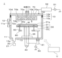
- FIG. 1 is an explanatory diagram schematically showing the configuration of a film forming apparatus as a substrate processing apparatus according to the present embodiment.
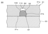
- FIG. 2 is a partially enlarged sectional view of the mounting table in FIG. 1;
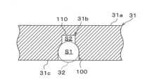
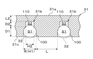
- FIG. 3 is a partially enlarged sectional view of the base material. It is a figure for explaining the dimensions of a base material.
- FIG. 7 is a partially enlarged cross-sectional view showing modification example 1 of the mounting table.
- FIG. 7 is a partially enlarged cross-sectional view showing a second modification of the mounting table.
- FIG. 7 is a partially enlarged cross-sectional view showing modification example 1 of the groove.
- FIG. 7 is a partially enlarged sectional view showing a second modification of the groove.
- FIG. 1 is an explanatory diagram schematically showing the configuration of a film forming apparatus as a substrate processing apparatus according to the present embodiment.
- FIG. 2 is a partially enlarged sectional view of the mounting table in FIG. 1;
- FIG. 3 is a
- FIG. 7 is a cross-sectional view showing a third modification of the mounting table.
- FIG. 7 is a diagram showing the results of a simulation performed regarding the temperature of the mounting surface for a wafer when the mounting surface for the wafer is heated by a heater inside the mounting table.
- FIG. 7 is a diagram showing the results of a simulation performed regarding the temperature of the mounting surface for a wafer when the mounting surface for the wafer is heated by a heater inside the mounting table.
- various substrate treatments such as film formation processing to form a predetermined film are performed on a substrate such as a semiconductor wafer (hereinafter referred to as a "wafer").
- This substrate processing is performed with the substrate placed on the mounting surface of the mounting table in the reduced pressure processing container.
- substrate processing may be performed with the substrate heated.
- heating of the substrate is performed by a heating device.
- the heating device has a base material formed in a plate shape and a heater formed in a linear shape and placed inside the base material, and by heating the base material with the heater, the temperature of the base material, which is a mounting surface, is increased.
- the substrate placed on the top surface is heated, or the substrate is heated via another member that has a placement surface and is disposed on the base material.
- the portion of the substrate directly above the heater may become hotter than the surrounding area. That is, a temperature distribution having the same shape as the arrangement pattern of the heaters may occur on the substrate. As a result, the arrangement pattern of the heaters may be transferred to the processing results of the substrate.
- the above-mentioned problems may occur in terms of responsiveness of heating of the substrate by the heater. Such thickening is not preferable.
- the technology according to the present disclosure improves the in-plane uniformity of heating the substrate by the heating device without increasing the thickness of the heating device that heats the substrate placed on it.
- FIG. 1 is an explanatory diagram schematically showing the configuration of a film forming apparatus as a substrate processing apparatus according to the present embodiment, and shows a part of the film forming apparatus in cross section.
- the film forming apparatus 1 in FIG. 1 is configured to process a wafer W as a substrate (specifically, perform a film forming process) and form a predetermined film on the wafer W.
- the film forming apparatus 1 includes a processing container 10 and a mounting table 30 as a heating device.
- the processing container 10 has a mounting table 30 installed therein, and is configured to be able to be depressurized.
- the processing container 10 has a container body 10a formed into a cylindrical shape with a bottom, for example.
- the container body 10a is formed using, for example, a metal material.
- a loading/unloading port 11a for the wafer W is provided in the side wall 11 of the container body 10a, and a gate valve 12 for opening/closing the loading/unloading port 11a is provided at the loading/unloading port 11a.
- An exhaust port 13a is formed in the bottom wall 13 of the container body 10a. Further, one end of an exhaust pipe 20 is connected to the exhaust port 13a. The other end of the exhaust pipe 20 is connected to an exhaust mechanism 21 having a vacuum pump or the like.
- the mounting table 30 includes a base material 31, a heater 32, and a lid member 33.
- the base material 31 is formed into a plate shape (specifically, a disk shape), and in this example, its upper surface constitutes a mounting surface 31a on which the wafer W is mounted.
- the base material 31 is made of a metal material with high thermal conductivity (for example, aluminum).
- the heater 32 is a linear sheath heater.
- One or more heaters 32 are disposed inside the base material 31 (specifically, inside a groove 31b described below) along the plate surface of the base material 31.
- a plurality of heaters 32 are arranged in a spiral shape in a plan view, and in the case of a plurality of heaters 32, each heater 32 is arranged in an annular shape and concentrically.
- the heaters 32 are arranged at equal intervals in a vertical cross-sectional view of the base material 31.
- the heater 32 is connected to a heater power source 40.
- the heater power source 40 is controlled by a control unit U, which will be described later.
- the lid member 33 is formed in a plate shape (specifically, a disk shape), and closes the opening of a groove 31b, which will be described later, in the base material 31.
- the lid member 33 is made of, for example, a metal material (for example, aluminum).
- a high frequency power source 50 for supplying high frequency power for bias is connected to the mounting table 30.
- the high frequency power source 50 is connected to, for example, the lid member 33 of the mounting table 30.
- the mounting table 30 is formed with a plurality of through holes 30a that penetrate in the vertical direction.
- a lift pin 60 which will be described later, is inserted into each through hole 30a. A more detailed structure of the mounting table 30 will be described later.
- the mounting table 30 is supported, for example, by a support member 35 erected at the center of the bottom of the processing container 10. Further, the mounting table 30 receives a lift pin 60 that is inserted into the above-described through hole 30a.
- the lift pins 60 are for transferring the wafer W between the mounting table 30 and a wafer transport device (not shown) inserted into the processing container 10 from outside the processing container 10 .
- This lift pin 60 is configured to be able to protrude from the mounting surface 31a of the mounting table 30 through the through hole 30a.
- the processing container 10 has a top wall member 10b that closes the upper opening of the container body 10a.
- the top wall member 10b is connected to the upper end of the container body 10a via an insulating member 10c having electrical insulation properties.
- the ceiling wall member 10b is formed using, for example, a metal material, and has a shower head 70 that injects processing gas into the processing space S.
- gas diffusion chambers 71a and 71b are provided within the shower head 70.
- the processing gas introduced into the gas diffusion chambers 70a, 70b is diffused in the horizontal direction within the gas diffusion chambers 70a, 70b, and then passed through the injection holes 72a, 72b, which are communicated with the gas diffusion chambers 70a, 70b, respectively. and is injected into the processing space S.
- a plurality of injection holes 72a and 72b are each provided.
- Each of the gas diffusion chambers 70a and 70b has one end connected to a supply mechanism (not shown) having a supply source of film forming gas, etc., and the other end of a supply pipe (not shown) connected to the other end.
- a sealing member 10d such as an O-ring is provided between the ceiling wall member 10b and the insulating member 10c to maintain airtightness. Further, a high frequency power source 51 for supplying high frequency power for plasma generation is connected to the ceiling wall member 10b via a matching circuit 52.
- a support member 80 and a moving mechanism 81 are provided for the lift pin 60.
- Support member 80 supports lift pin 60.
- the support member 80 is formed, for example, in an annular shape in a plan view.
- the moving mechanism 81 raises and lowers the lift pin 60 by raising and lowering the support member 80.
- the moving mechanism 81 has a drive source (not shown) such as a motor that generates a drive force to move the support member 80 up and down.
- the film forming apparatus 1 configured as described above is provided with a control unit U.
- the control unit U is constituted by a computer including a processor such as a CPU and a memory, and has a program storage unit (not shown).
- the program storage unit stores a program for realizing processing of the wafer W by the film forming apparatus 1.
- the above program may be one that has been recorded on a computer-readable storage medium, and may have been installed in the control unit U from the storage medium. Further, the storage medium may be temporary or non-temporary.
- FIG. 2 is a partially enlarged sectional view of the mounting table 30.
- FIG. 3 is a partially enlarged sectional view of the base material 31.
- FIG. 4 is a diagram for explaining the dimensions of the base material 31.
- the mounting table 30 includes the base material 31, the heater 32, and the lid member 33. As shown in FIGS. 2 and 3, the base material 31 has a groove 31b in which the heater 32 is fixed.
- the groove 31b is recessed from the side opposite to the wafer W side of the base material 31 toward the wafer W side, that is, recessed upward from the lower surface 31c of the base material 31 facing the mounting surface 31a. is formed.
- the shape of the groove 31b in plan view corresponds to the arrangement pattern of the heater 32, for example, a spiral shape or an annular shape (specifically, a circular shape) centered on the center of the base material 31 circular).
- This groove 31b has a contact portion 100 that contacts the heater 32 on the front side, that is, on the lower side, and has a non-contact portion 110 that does not contact the heater 32 on the back side, that is, on the upper side.
- the contact portion 100 is formed, for example, so that most of it is in contact with the heater 32.
- the contact portion 100 is open on the front side and the back side, that is, the lower side and the upper side, and forms a space S1 in which at least half of the heater 32 is accommodated.
- the heater 32 is positioned in the vertical direction inside the base material 31 by the rear end, that is, the upper end of the contact portion 100.
- the non-contact portion 110 is formed so that its entirety does not come into contact with the heater 32 at all.
- This non-contact portion 110 forms a space S2 with an open front side, that is, a lower side. Specifically, the space S2 is open toward the space S1.
- the non-contact portion 110 is formed to be further recessed from the inner end, that is, the upper end, of the contact portion 100 that is recessed from the lower surface of the base material 31.
- the space S2 formed by the non-contact portion 110 has, for example, a rectangular shape in a cross-sectional view (that is, a longitudinal cross-sectional view) in the extending direction of the groove 31b.
- the space S1 formed by the contact portion 100 has a shape, for example, in which a semicircle is connected to the upper end of a rectangle in a longitudinal cross-sectional view.
- the lid member 33 is fixed to the base material 31 in such a manner that it closes the lower opening of the groove 31b and crushes the heater 32 between the contact portion 100 and the lid member 33. .
- the base material 31 and the lid member 33 are fixed by, for example, brazing.
- the heater 32 has, for example, a circular cross-sectional shape in a state where no external pressure such as crushing from the lid member 33 is applied.
- the diameter of the heater 32 in a longitudinal section view means the diameter of the heater 32 in a longitudinal section view in a state where the above-mentioned external pressure is not applied.
- the diameter R (see FIG. 4) of the heater 32 in a longitudinal cross-sectional view is, for example, 5 mm to 10 mm. Further, in a longitudinal cross-sectional view, the distance L1 between adjacent heaters 32 is, for example, 1.5 times or more the diameter R of the heaters 32.
- the width H1 of the space S1 formed by the contact portion 100 of the groove 31b of the base material 31 is approximately equal to the diameter R of the heater 32.
- the depth D1 of the contact portion 100 is such that when the heater 32 is accommodated in the groove 31b and the opening of the groove 31b is not covered by the lid member 33, a portion of the heater 32 is The depth is such that it protrudes from the lower surface 31c of the base material 31.
- the width H2 of the open portion on the front side, that is, the lower side, of the space S2 formed by the non-contact portion 110 is, for example, 15% or more of the diameter (i.e., thickness) R of the heater 32, and more preferably It is 75% or more.
- the width H2 is preferably 90% or less of the diameter of the heater 32.
- the depth D2 of the non-contact portion 110 is, for example, 20 to 100% of the diameter R of the heater 32.
- the distance L2 from the upper end of the non-contact part 110 to the surface on the wafer W side, that is, the mounting surface 31a is, for example, 15% to 60% of the diameter R of the heater 32. is 1 mm to 4 mm. By setting the distance L2 to 4 mm or less, the thickness of the mounting table 30 can be suppressed.
- Step S1 Placement
- the wafer W is placed on the mounting surface 31a of the mounting table 30.
- the gate valve 12 provided at the loading/unloading port 11a of the wafer W of the processing container 10 is opened, and the loading/unloading port 11a is opened from a transfer chamber (not shown) in a vacuum atmosphere adjacent to the processing container 10.
- a transport mechanism (not shown) holding the wafer W is inserted into the processing chamber 10 in a vacuum atmosphere.
- the wafer W is transported above the mounting table 30.
- the wafer W is transferred onto the lifted lift pins 60, and then the transfer mechanism is taken out from the processing container 10, and the gate valve 12 is closed.
- the lift pins 60 are lowered, and the wafer W is placed on the mounting surface 31a of the mounting table 30 whose temperature is adjusted to a predetermined temperature by the heater 32.
- the heater 32 is provided in the groove 31b, and the non-contact portion 110 exists between the heater 32 and the surface of the base material 31 on the wafer W side, that is, the mounting surface 31a.
- the upper part of the heater 32 near the mounting surface 31a does not contact the base material 31. Therefore, almost no heat from the upper part of the heater 32 is transmitted to the mounting surface 31a.
- the portion of the heater 32 that comes into contact with the base material 31 is other than the upper portion. Since the portion of the heater 32 other than the upper portion is far from the mounting surface 31a, the heat from the portion is easily spread in the horizontal direction and then transmitted to the mounting surface 31a.
- the placement surface 31a is heated more uniformly within the surface by the heater 32, and the placement surface 31a is heated more uniformly within the surface.
- the placed wafer W is also heated more uniformly within the surface.
- Step S2 Film formation
- processing gas including film-forming gas is supplied from the shower head 70, high-frequency power for biasing is supplied from the high-frequency power supply 50, and high-frequency power for plasma generation is supplied from the high-frequency power supply 51.
- the wafer W is processed by the plasma of the processing gas, and a predetermined film is formed on the wafer W.
- the supply of processing gas from the shower head 70, the high frequency power for bias from the high frequency power supply 50, and the supply of high frequency power for plasma generation from the high frequency power supply 51 are stopped.
- the wafer W is carried out from the processing container 10 in the reverse order of step S1.
- the in-plane uniformity of heating of the wafer W placed on the mounting table 30 by the mounting table 30 can be improved. That is, it is possible to prevent the arrangement pattern of the heaters 32 from being transferred to the temperature distribution of the wafer W heated by the mounting table 30 or the film formation result of the wafer W.
- the above-described in-plane uniformity of heating can be improved without increasing the thickness of the mounting table 30. Therefore, due to the thickening of the mounting table 30, - Decrease in the responsiveness of heating the wafer W by the heater 32; ⁇ Deterioration in handling of the mounting table 30, - Increased cost of the mounting table 30, ⁇ Increase in energy consumption, etc. can be suppressed. Furthermore, since the mounting table 30 can be prevented from becoming thicker, the space inside the processing container 10 in which the mounting table 30 is installed can be effectively utilized.
- FIG. 5 is a partially enlarged sectional view showing Modification Example 1 of the mounting table.
- the mounting table 30 is the heating device itself according to the present disclosure, and the upper surface of the base material 31 of the mounting table 30 is the mounting surface 31a for the wafer W, and the wafer is directly placed on the mounting table 30, that is, the heating device. W was placed there.
- the mounting table 30A in FIG. 5 includes a heating device 200 having a base material 31, a heater 32, and a lid member 33, and a static stand which is an example of another member having a mounting surface 211 on which the wafer W is mounted.
- the electrostatic chuck 210 is fixed to the surface of the heating device 200 on the wafer W side, that is, the upper surface 201 of the base material 31. That is, the wafer W is indirectly placed on the heating device 200 via the electrostatic chuck 210 . Then, this heating device 200 heats the wafer W indirectly placed on the heating device 200.
- the electrostatic chuck 210 is a member that attracts and holds the wafer W placed on the mounting surface 211 by electrostatic force. This is a low plate-like member in which an electrode for electrostatic adsorption is embedded. Therefore, the temperature distribution on the mounting surface 211 of the electrostatic chuck 210 has the same shape as the arrangement pattern of the heaters 32, and the temperature of the wafer W placed on the mounting surface 211 may become non-uniform within the surface. In contrast, in this example, since the heating device 200 has the above-mentioned groove 31b in the base material 31, the in-plane uniformity of heating by the heating device 200 of the wafer W indirectly placed on the heating device 200 is improved. can do.
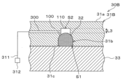
- FIG. 6 is a partially enlarged sectional view showing a second modification of the mounting table.
- an exhaust path 300 is formed in the base material 31B.
- One end of the exhaust path 300 communicates with the space S2 formed by the non-contact portion 110 of the groove 31b, and the other end of the exhaust path 300 communicates with an exhaust mechanism 311 having a vacuum pump or the like via an exhaust pipe 310. It is connected to the. Thereby, the inside of space S2 can be exhausted. Therefore, the upper part of the heater 32 and the non-contact portion 110 of the groove 31b can be vacuum-insulated. Therefore, local heating of the base material 31B directly above the heater 32 can be further suppressed. Therefore, according to this example, the in-plane uniformity of heating of the wafer W placed on the mounting table 30B by the mounting table 30B can be further improved.
- FIGS. 7 and 8 are partially enlarged cross-sectional views showing Modification 1 and Modification 2 of the groove in which the heater 32 is fixed, respectively.
- the space S2 formed by the non-contact portion 110 of the groove 31b had the same horizontal width in the lower open portion and the upper portion when viewed in longitudinal section.
- the space S2 formed by the non-contact portion 401 of the groove 400 of the base material 31C has a width in the horizontal direction in a longitudinal cross-sectional view that is larger than that of the lower open part. Portions can be large. Thereby, the heat from the heater 32 can be spread more horizontally before being transmitted to the mounting surface 31a, and the in-plane uniformity of heating can be further improved.
- the width H3 of the upper part of the space S2 is such that the distance L3 between the adjacent spaces S2 is larger than the diameter of the heater 32, and is 120% of the diameter R of the heater 32. It is preferable that it is below. Thereby, it is possible to suppress the formation pattern of the space S2 in plan view from being transferred to the temperature distribution of the wafer W heated by the mounting table having the grooves 400, etc.
- the space S2 formed by the non-contact portion 501 of the groove 500 of the base material 31D is formed such that the width in the horizontal direction increases toward the back side, that is, toward the top, in a longitudinal cross-sectional view. You can leave it there.
- the heat from the heater 32 can be spread more horizontally before being transmitted to the mounting surface 31a, and the in-plane uniformity of heating can be further improved.
- the width H4 of the upper end of the space S2 is such that the distance L3 between adjacent spaces S2 is larger than the diameter R of the heater 32, and is 120% or less of the diameter R of the heater 32. It is preferable that there be. Thereby, it is possible to suppress the formation pattern of the space S2 in a plan view from being transferred to the temperature distribution of the wafer W heated by the mounting table having the grooves 500, etc.
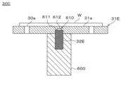
- FIG. 9 is a sectional view showing a third modification of the mounting table.
- the heater 32 was a sheath heater, but in this example, the heater 32E is a linear cartridge heater.
- the mounting table 30C of this example includes one heater 32E that is a cartridge heater, a support member 600, and a base material 31E.
- the support member 600 is erected at the center of the bottom of the processing container 10 and supports the base material 31E.
- the lower part of the heater 32E is fixed within the support member 600, and the upper part thereof is fixed within the base material 31E.
- the base material 31E has a groove 610 in which the upper part of the heater 32E is fixed.
- the groove 610 has a contact portion 611 on the lower side that contacts the heater 32E, and a non-contact portion 612 on the upper side that does not contact the top of the heater 32E.
- the heater 32E When the heater 32E is provided as in this example, only the central portion of the mounting surface 31a may become locally hot. However, in this example, a non-contact portion 612 is provided above the groove 610 in which the heater 32E is fixed. Therefore, almost no heat from the center of the upper end surface of the heater 32E is transmitted to the mounting surface 31a. Therefore, according to this example, it is possible to prevent only the central portion of the mounting surface 31a from becoming locally heated.
- Test example The present inventors simulated the temperature of the mounting surface for a wafer when the mounting surface for the wafer was heated by a heater inside the mounting table.
- 10 and 11 are diagrams showing the results of the above simulation, respectively.
- FIG. 10 shows the results of Test Example 1
- FIG. 11 shows the results of Test Example 2.
- FIG. 10 and FIG. 11 show the temperature of the mounting surface in shading; the higher the temperature, the darker it is, and the lower the temperature, the lighter it is.
- Test Example 1 and Test Example 2 differ only in the structure of the groove of the mounting table.
- the mounting table in Test Example 2 has the groove 31b shown in FIG. 4, whereas the mounting table in Test Example 1 has a groove that does not have the non-contact part 110, the heater contacts the entire groove, and the upper part of the heater was also in contact with the ditch.
- the mounting table in Test Example 1 will also be explained using the same reference numerals as the mounting table 30 in Test Example 2.
- the main simulation conditions other than the structure of the groove 31b are as follows.
- ⁇ Material of base material 31 of mounting table 30 Aluminum ⁇ Type of heater 32: Sheath heater ⁇ Distance from mounting surface 31a of mounting table 30 to upper end of heater 32: 3.5 mm ⁇ Cross-sectional shape of heater 32: circular ⁇ Diameter of heater 32: 6.5 mm - Arrangement pattern of heater 32: one in an annular shape centered on the center of mounting surface 31a - Width H2 of space S2 in test example 2: 5 mm - Distance L2 from the upper end of the non-contact part 110 to the mounting surface 31a in Test Example 2: 1.5 mm - Distance L3 from the innermost part of the groove 31b to the upper end of the heater 32 in Test Example 2: 2 mm
- the technology according to the present disclosure was applied to a heating device that heats a substrate placed directly or indirectly through another member.
- the technology according to the present disclosure can also be applied to a heating device that heats an object to be heated that comes into contact with the object directly or indirectly through another member.
Landscapes
- Chemical & Material Sciences (AREA)
- General Chemical & Material Sciences (AREA)
- Chemical Kinetics & Catalysis (AREA)
- Engineering & Computer Science (AREA)
- Materials Engineering (AREA)
- Mechanical Engineering (AREA)
- Metallurgy (AREA)
- Organic Chemistry (AREA)
- Chemical Vapour Deposition (AREA)
- Container, Conveyance, Adherence, Positioning, Of Wafer (AREA)
Abstract
Description
ヒータが内部に配置される基材を厚くすること等により、加熱装置による基板の加熱の面内均一性の改善を図ることはできるが、ヒータによる基板の加熱の応答性等の面で上述のような厚型化は好ましくない。
図1は、本実施形態にかかる基板処理装置としての成膜装置の構成の概略を模式的に示す説明図であり、成膜装置の一部を断面で示している。
処理容器10は、その内部に載置台30が設置されるものであり、減圧可能に構成されている。この処理容器10は、例えば有底の円筒状に形成された容器本体10aを有する。
基材31は、板状(具体的には円板状)に形成されており、本例において、その上面が、ウェハWが載置される載置面31aを構成する。基材31は、熱伝導率が高い金属材料(例えばアルミニウム)から形成されている。
載置台30のより詳細な構造は後述する。
また、載置台30に対して、上述の貫通孔30aに挿通されるリフトピン60が受けられている。リフトピン60は、処理容器10の外部から当該処理容器10内に挿入されるウェハ搬送装置(図示せず)と載置台30との間でウェハWを受け渡すためのものである。このリフトピン60は、載置台30の載置面31aから貫通孔30aを介して突出可能に構成されている。
さらに、天壁部材10bには、プラズマ生成用の高周波電力を供給するための高周波電源51がマッチング回路52を介して接続されている。
続いて、載置台30の構造の詳細について説明する。図2は、載置台30の部分拡大断面図である。図3は、基材31の部分拡大断面図である。図4は、基材31の寸法を説明するための図である。
基材31は、図2及び図3に示すように、内部にヒータ32が固定される溝31bを有する。
この溝31bは、ヒータ32と接触する接触部100を手前側すなわち下側に有し、ヒータ32と接触しない非接触部110を奥側すなわち上側に有する。
ヒータ32は、図3に示すように、蓋部材33等による圧し潰すような外圧が作用していない状態において、例えば断面視円形状である。なお、以下において、「縦断面視におけるヒータ32の直径」とは、上述の外圧が作用していない状態での縦断面視におけるヒータ32の直径を意味する
縦断面視におけるヒータ32の直径R(図4参照)は、例えば5mm~10mmである。また、縦断面視において、隣り合うヒータ32間の距離L1は、例えばヒータ32の直径Rの1.5倍以上である。
また、縦断面視において、接触部100の深さD1は、溝31bにヒータ32が収まっている状態且つ溝31bの開口が蓋部材33に塞がれていない状態で、ヒータ32の一部が基材31の下面31cから突出するような深さである。
また、縦断面視において、非接触部110の深さD2は、例えば、ヒータ32の直径Rの20~100%である。
続いて、成膜装置1によるウェハWの処理の一例を説明する。なお、このウェハWの処理は、制御部Uの制御の下、行われる。
まず、載置台30の載置面31aにウェハWが載置される。
具体的には、例えば、処理容器10のウェハWの搬入出口11aに設けられたゲートバルブ12が開かれ、処理容器10に隣接する真空雰囲気の搬送室(図示せず)から、搬入出口11aを介して、ウェハWを保持した搬送機構(図示せず)が真空雰囲気の処理容器10内に挿入される。そして、ウェハWが、載置台30の上方に搬送される。次いで上昇したリフトピン60の上にウェハWが受け渡され、その後、上記搬送機構は処理容器10から抜き出され、ゲートバルブ12が閉じられる。それと共に、リフトピン60の下降が行われ、ヒータ32により所定の温度に調整された載置台30の載置面31a上にウェハWが載置される。
また、ヒータ32のうち、基材31と接触するのは、上部以外の部分である。ヒータ32の上部以外の部分は、載置面31aから遠いため、当該部分からの熱は水平方向に拡散されてから載置面31aに伝わりやすい。
その後、ウェハW上に所定の膜が形成される。
具体的には、例えば、シャワーヘッド70からの成膜ガスを含む処理ガスの供給、高周波電源50からのバイアス用の高周波電力、高周波電源51からのプラズマ生成用の高周波電力の供給が行われる。これにより、処理ガスのプラズマによってウェハWが処理され、当該ウェハW上に所定の膜が形成される。
以上のように、本実施形態によれば、載置台30に載置されたウェハWの当該載置台30による加熱の面内均一性を改善することができる。すなわち、ヒータ32の配設パターンが、載置台30により加熱されたウェハWの温度分布やウェハWの成膜結果に転写されるのを抑制することができる。
・ヒータ32によるウェハWの加熱の応答性の低下、
・載置台30の取り扱い性の悪化、
・載置台30の高コスト化、
・エネルギー消費量の増加、
等を抑制することができる。また、載置台30の厚型化を抑制できるため、載置台30が設置される処理容器10の内部の空間を有効利用することができる。
図5は、載置台の変形例1を示す部分拡大断面図である。
以上の例では、載置台30が本開示にかかる加熱装置そのものであり、載置台30の基材31の上面がウェハWに対する載置面31aとなっており、載置台30すなわち加熱装置に直接ウェハWが載置されていた。
図6は、載置台の変形例2を示す部分拡大断面図である。
図6の載置台30Bは、基材31Bに排気路300が形成されている。排気路300の一端部は、溝31bの非接触部110により形成される空間S2に連通しており、排気路300の他端部は、排気管310を介して真空ポンプ等を有する排気機構311に接続されている。これにより、空間S2内を排気することができる。そのため、ヒータ32の上部と、溝31bの非接触部110とを真空断熱することができる。したがって、基材31Bにおけるヒータ32の上部の直上が局所的に加熱されるのをさらに抑制することができる。よって、本例によれば、載置台30Bに載置されたウェハWの当該載置台30Bによる加熱の面内均一性をさらに改善することができる。
図7及び図8はそれぞれ、内部にヒータ32が固定される溝の変形例1及び変形例2を示す部分拡大断面図である。
以上の例では、溝31bの非接触部110により形成される空間S2は、縦断面視における水平方向の幅が、下側の開放部分と、それより上側の部分とで同じであった。
この場合、縦断面視において、空間S2の上記上側の部分の幅H3は、隣り合う空間S2間の距離L3がヒータ32の直径より大きくなる幅であり、また、ヒータ32の直径Rの120%以下であることが好ましい。これにより、平面視における空間S2の形成パターンが、溝400を有する載置台により加熱されたウェハWの温度分布等に転写されるのを抑制することができる。
図9は、載置台の変形例3を示す断面図である。
以上の例では、ヒータ32がシースヒータであったが、本例ではヒータ32Eは線状に形成されたカートリッジヒータである。
本例の載置台30Cは、カートリッジヒータであるヒータ32Eを1本と、支持部材600と、基材31Eと、を有する。
ヒータ32Eは、その下部が支持部材600内で固定され、その上部が基材31E内で固定される。
本発明者らは、載置台の内部のヒータでウェハに対する載置面を加熱したときの当該載置面の温度についてシミュレーションを行った。図10及び図11はそれぞれ、上記シミュレーションの結果を示す図であり、図10は試験例1の結果を示し、図11は試験例2の結果を示している。また、図10及び図11は、載置面の温度を濃淡で示しており、温度が高いほど濃く示し、低いほど薄く示している。
・載置台30の基材31の材料:アルミニウム
・ヒータ32の種類:シースヒータ
・載置台30の載置面31aからヒータ32の上端までの距離:3.5mm
・ヒータ32の断面形状:円形状
・ヒータ32の直径:6.5mm
・ヒータ32の配設パターン:載置面31aの中心を中心とした円環状に1本
・試験例2における空間S2の幅H2:5mm
・試験例2における非接触部110の上端から載置面31aまでの距離L2:1.5mm
・試験例2における溝31bの最奥部からヒータ32の上端までの距離L3:2mm
それに対し、試験例2では、図11に示すように、試験例1に比べて、全体的に載置面31aの温度が均一になっていた。この結果からも、ヒータ32が内部に固定される溝31bに、非接触部110を形成することにより、載置台30によるウェハWの加熱の面内均一性を改善することができることが分かる。
以上の実施形態では、直接的または他の部材を介して間接的に載置される基板を加熱する加熱装置に本開示にかかる技術が適用されていた。
本開示にかかる技術は、直接的または他の部材を介して間接的に接触する加熱対象体を加熱する加熱装置にも適用することができる。
31、31B、31C、31D、31E 基材
31b、400、500、610 溝
32、32E ヒータ
100、611 接触部
110、401、501、612 非接触部
200 加熱装置
W ウェハ
Claims (7)
- 直接的または他の部材を介して間接的に載置される基板を加熱する加熱装置であって、
線状のヒータと、
前記基板側とは反対側から前記基板側に向けて凹み、内部に前記ヒータが固定される溝を有する基材と、を有し、
前記溝は、前記ヒータと接触する接触部を手前側に有し、前記ヒータと接触しない非接触部を奥側に有する、加熱装置。 - 前記非接触部は、手前側が開放された空間を形成する、請求項1に記載の加熱装置。
- 前記溝の延在方向の断面視断面視において、前記空間の手前側の開放部分の幅は、前記ヒータの太さの75%以上である、請求項2に記載の加熱装置。
- 前記空間は、前記溝の延在方向の断面視において矩形状である、請求項2または3に記載の加熱装置。
- 前記空間は、前記溝の延在方向の断面視において奥側に向けて幅が拡がるように形成されている、請求項2または3に記載の加熱装置。
- 前記基材は、前記空間に連通する排気路を有する、請求項2または3に記載の加熱装置。
- 請求項1に記載の加熱装置と、当該加熱装置が内部に設置される処理容器と、を備える、基板処理装置。
Priority Applications (3)
| Application Number | Priority Date | Filing Date | Title |
|---|---|---|---|
| CN202380036865.0A CN119137728A (zh) | 2022-05-10 | 2023-04-26 | 加热装置和基板处理装置 |
| KR1020247039601A KR102950456B1 (ko) | 2022-05-10 | 2023-04-26 | 가열 장치 및 기판 처리 장치 |
| US18/941,290 US20250069912A1 (en) | 2022-05-10 | 2024-11-08 | Heating device and substrate processing apparatus |
Applications Claiming Priority (2)
| Application Number | Priority Date | Filing Date | Title |
|---|---|---|---|
| JP2022-077487 | 2022-05-10 | ||
| JP2022077487A JP2023166746A (ja) | 2022-05-10 | 2022-05-10 | 加熱装置及び基板処理装置 |
Related Child Applications (1)
| Application Number | Title | Priority Date | Filing Date |
|---|---|---|---|
| US18/941,290 Continuation US20250069912A1 (en) | 2022-05-10 | 2024-11-08 | Heating device and substrate processing apparatus |
Publications (1)
| Publication Number | Publication Date |
|---|---|
| WO2023218963A1 true WO2023218963A1 (ja) | 2023-11-16 |
Family
ID=88730373
Family Applications (1)
| Application Number | Title | Priority Date | Filing Date |
|---|---|---|---|
| PCT/JP2023/016465 Ceased WO2023218963A1 (ja) | 2022-05-10 | 2023-04-26 | 加熱装置及び基板処理装置 |
Country Status (5)
| Country | Link |
|---|---|
| US (1) | US20250069912A1 (ja) |
| JP (1) | JP2023166746A (ja) |
| KR (1) | KR102950456B1 (ja) |
| CN (1) | CN119137728A (ja) |
| WO (1) | WO2023218963A1 (ja) |
Cited By (1)
| Publication number | Priority date | Publication date | Assignee | Title |
|---|---|---|---|---|
| WO2025229913A1 (ja) * | 2024-04-30 | 2025-11-06 | 京セラ株式会社 | 試料支持体 |
Citations (3)
| Publication number | Priority date | Publication date | Assignee | Title |
|---|---|---|---|---|
| JP2006108011A (ja) * | 2004-10-08 | 2006-04-20 | Furukawa Sky Kk | ヒータプレート及びヒータプレートの製造方法 |
| JP2006111973A (ja) * | 2004-10-13 | 2006-04-27 | Applied Materials Inc | 加熱基板支持体及びその製造方法 |
| JP2009535801A (ja) * | 2006-04-28 | 2009-10-01 | ダンスン エレクトロン カンパニー リミテッド | サセプタの製造方法、及び、この方法によって製造されたサセプタ |
Family Cites Families (3)
| Publication number | Priority date | Publication date | Assignee | Title |
|---|---|---|---|---|
| JP5347214B2 (ja) | 2006-06-12 | 2013-11-20 | 東京エレクトロン株式会社 | 載置台構造及び熱処理装置 |
| JP2011054838A (ja) | 2009-09-03 | 2011-03-17 | Tokyo Electron Ltd | 載置台構造及び処理装置 |
| KR101337463B1 (ko) * | 2013-08-09 | 2013-12-05 | 주식회사 포톤 | 균일한 온도 분포를 갖는 서셉터 및 그 제조방법 |
-
2022
- 2022-05-10 JP JP2022077487A patent/JP2023166746A/ja active Pending
-
2023
- 2023-04-26 CN CN202380036865.0A patent/CN119137728A/zh active Pending
- 2023-04-26 WO PCT/JP2023/016465 patent/WO2023218963A1/ja not_active Ceased
- 2023-04-26 KR KR1020247039601A patent/KR102950456B1/ko active Active
-
2024
- 2024-11-08 US US18/941,290 patent/US20250069912A1/en active Pending
Patent Citations (3)
| Publication number | Priority date | Publication date | Assignee | Title |
|---|---|---|---|---|
| JP2006108011A (ja) * | 2004-10-08 | 2006-04-20 | Furukawa Sky Kk | ヒータプレート及びヒータプレートの製造方法 |
| JP2006111973A (ja) * | 2004-10-13 | 2006-04-27 | Applied Materials Inc | 加熱基板支持体及びその製造方法 |
| JP2009535801A (ja) * | 2006-04-28 | 2009-10-01 | ダンスン エレクトロン カンパニー リミテッド | サセプタの製造方法、及び、この方法によって製造されたサセプタ |
Cited By (1)
| Publication number | Priority date | Publication date | Assignee | Title |
|---|---|---|---|---|
| WO2025229913A1 (ja) * | 2024-04-30 | 2025-11-06 | 京セラ株式会社 | 試料支持体 |
Also Published As
| Publication number | Publication date |
|---|---|
| CN119137728A (zh) | 2024-12-13 |
| JP2023166746A (ja) | 2023-11-22 |
| KR20250005418A (ko) | 2025-01-09 |
| US20250069912A1 (en) | 2025-02-27 |
| KR102950456B1 (ko) | 2026-04-09 |
Similar Documents
| Publication | Publication Date | Title |
|---|---|---|
| JP3889074B2 (ja) | 低圧化学蒸着装置 | |
| CN1919768B (zh) | 可主动冷却的基板支撑件 | |
| US6805749B2 (en) | Method and apparatus for supporting a semiconductor wafer during processing | |
| CN101533797B (zh) | 载置台构造以及热处理装置 | |
| KR100854500B1 (ko) | 척 어셈블리 및 이를 구비한 고밀도 플라즈마 설비 | |
| KR20030097861A (ko) | 열 분산 플레이트 및 에지 지지대를 구비하는 어셈블리 | |
| CN101924017A (zh) | 基板加热单元和包含该基板加热单元的基板处理装置 | |
| TWI829326B (zh) | 基板處理裝置 | |
| TW201903903A (zh) | 熱處理方法 | |
| JP5003663B2 (ja) | 真空加熱装置 | |
| JP2020088193A (ja) | プラズマ処理装置及びプラズマ処理方法 | |
| WO2023218963A1 (ja) | 加熱装置及び基板処理装置 | |
| KR19990071713A (ko) | 피처리 기판을 가열하면서 처리 가스를 이용하는반도체 처리방법 및 그 장치 | |
| JP2001110885A (ja) | 半導体処理装置および半導体処理方法 | |
| TW201730968A (zh) | 基板的熱處理裝置及方法以及基板的接收單元 | |
| JP2015076457A (ja) | 基板処理装置 | |
| JP7498743B2 (ja) | 基板処理装置及び基板処理方法 | |
| TWI780314B (zh) | 基板加熱裝置及使用其之基板處理裝置 | |
| US20080017111A1 (en) | Semiconductor Manufacturing Device and Method for Manufacturing Semiconductor Devices | |
| KR100542629B1 (ko) | 반도체 소자 제조 장치 및 방법 | |
| KR102778057B1 (ko) | 기판 탑재 방법 및 기판 탑재 기구 | |
| JP2005259902A (ja) | 基板処理装置 | |
| KR101749311B1 (ko) | 기판 지지 유닛 및 이를 포함하는 기판 처리 장치 | |
| KR100688485B1 (ko) | 웨이퍼지지대에 냉각라인을 구비한 챔버장치 및 이를이용한 웨이퍼 처리공정 | |
| JP2005093886A (ja) | 半導体製造装置 |
Legal Events
| Date | Code | Title | Description |
|---|---|---|---|
| 121 | Ep: the epo has been informed by wipo that ep was designated in this application |
Ref document number: 23803442 Country of ref document: EP Kind code of ref document: A1 |
|
| WWE | Wipo information: entry into national phase |
Ref document number: 202380036865.0 Country of ref document: CN |
|
| ENP | Entry into the national phase |
Ref document number: 20247039601 Country of ref document: KR Kind code of ref document: A |
|
| NENP | Non-entry into the national phase |
Ref country code: DE |
|
| 122 | Ep: pct application non-entry in european phase |
Ref document number: 23803442 Country of ref document: EP Kind code of ref document: A1 |