WO2023175690A1 - プラズマ処理装置 - Google Patents
プラズマ処理装置 Download PDFInfo
- Publication number
- WO2023175690A1 WO2023175690A1 PCT/JP2022/011436 JP2022011436W WO2023175690A1 WO 2023175690 A1 WO2023175690 A1 WO 2023175690A1 JP 2022011436 W JP2022011436 W JP 2022011436W WO 2023175690 A1 WO2023175690 A1 WO 2023175690A1
- Authority
- WO
- WIPO (PCT)
- Prior art keywords
- region
- heater
- regions
- plasma processing
- wafer
- Prior art date
Links
- 238000009832 plasma treatment Methods 0.000 title description 2
- 239000000463 material Substances 0.000 claims description 36
- 239000007769 metal material Substances 0.000 claims description 5
- 235000012431 wafers Nutrition 0.000 description 76
- 239000004065 semiconductor Substances 0.000 description 13
- 238000005530 etching Methods 0.000 description 11
- 239000007789 gas Substances 0.000 description 11
- 230000005684 electric field Effects 0.000 description 10
- 238000000034 method Methods 0.000 description 8
- 238000004519 manufacturing process Methods 0.000 description 6
- 239000004020 conductor Substances 0.000 description 5
- 230000007423 decrease Effects 0.000 description 5
- 230000002093 peripheral effect Effects 0.000 description 5
- 230000001788 irregular Effects 0.000 description 4
- 239000002245 particle Substances 0.000 description 4
- 239000003507 refrigerant Substances 0.000 description 4
- 239000003989 dielectric material Substances 0.000 description 3
- 239000000047 product Substances 0.000 description 3
- ZOKXTWBITQBERF-UHFFFAOYSA-N Molybdenum Chemical compound [Mo] ZOKXTWBITQBERF-UHFFFAOYSA-N 0.000 description 2
- 240000004050 Pentaglottis sempervirens Species 0.000 description 2
- 235000004522 Pentaglottis sempervirens Nutrition 0.000 description 2
- RTAQQCXQSZGOHL-UHFFFAOYSA-N Titanium Chemical compound [Ti] RTAQQCXQSZGOHL-UHFFFAOYSA-N 0.000 description 2
- 239000000919 ceramic Substances 0.000 description 2
- 239000001307 helium Substances 0.000 description 2
- 229910052734 helium Inorganic materials 0.000 description 2
- SWQJXJOGLNCZEY-UHFFFAOYSA-N helium atom Chemical compound [He] SWQJXJOGLNCZEY-UHFFFAOYSA-N 0.000 description 2
- 230000001771 impaired effect Effects 0.000 description 2
- 150000002500 ions Chemical class 0.000 description 2
- 229910052751 metal Inorganic materials 0.000 description 2
- 239000002184 metal Substances 0.000 description 2
- 229910052750 molybdenum Inorganic materials 0.000 description 2
- 239000011733 molybdenum Substances 0.000 description 2
- 230000000149 penetrating effect Effects 0.000 description 2
- 238000003672 processing method Methods 0.000 description 2
- 239000010453 quartz Substances 0.000 description 2
- VYPSYNLAJGMNEJ-UHFFFAOYSA-N silicon dioxide Inorganic materials O=[Si]=O VYPSYNLAJGMNEJ-UHFFFAOYSA-N 0.000 description 2
- 239000000758 substrate Substances 0.000 description 2
- 229910052719 titanium Inorganic materials 0.000 description 2
- 239000010936 titanium Substances 0.000 description 2
- WFKWXMTUELFFGS-UHFFFAOYSA-N tungsten Chemical compound [W] WFKWXMTUELFFGS-UHFFFAOYSA-N 0.000 description 2
- 229910052721 tungsten Inorganic materials 0.000 description 2
- 239000010937 tungsten Substances 0.000 description 2
- 229910052782 aluminium Inorganic materials 0.000 description 1
- XAGFODPZIPBFFR-UHFFFAOYSA-N aluminium Chemical compound [Al] XAGFODPZIPBFFR-UHFFFAOYSA-N 0.000 description 1
- PNEYBMLMFCGWSK-UHFFFAOYSA-N aluminium oxide Inorganic materials [O-2].[O-2].[O-2].[Al+3].[Al+3] PNEYBMLMFCGWSK-UHFFFAOYSA-N 0.000 description 1
- 238000005513 bias potential Methods 0.000 description 1
- 230000005540 biological transmission Effects 0.000 description 1
- 229910010293 ceramic material Inorganic materials 0.000 description 1
- 239000007795 chemical reaction product Substances 0.000 description 1
- 150000001875 compounds Chemical class 0.000 description 1
- 239000002826 coolant Substances 0.000 description 1
- 238000010586 diagram Methods 0.000 description 1
- 238000010494 dissociation reaction Methods 0.000 description 1
- 230000005593 dissociations Effects 0.000 description 1
- 230000000694 effects Effects 0.000 description 1
- 230000005611 electricity Effects 0.000 description 1
- 230000005284 excitation Effects 0.000 description 1
- 230000014509 gene expression Effects 0.000 description 1
- 230000020169 heat generation Effects 0.000 description 1
- 239000011810 insulating material Substances 0.000 description 1
- 230000010354 integration Effects 0.000 description 1
- 230000003993 interaction Effects 0.000 description 1
- 238000002844 melting Methods 0.000 description 1
- 230000008018 melting Effects 0.000 description 1
- TWNQGVIAIRXVLR-UHFFFAOYSA-N oxo(oxoalumanyloxy)alumane Chemical compound O=[Al]O[Al]=O TWNQGVIAIRXVLR-UHFFFAOYSA-N 0.000 description 1
- 239000011347 resin Substances 0.000 description 1
- 229920005989 resin Polymers 0.000 description 1
- 229910052710 silicon Inorganic materials 0.000 description 1
- 239000010703 silicon Substances 0.000 description 1
- 238000001179 sorption measurement Methods 0.000 description 1
- 230000003068 static effect Effects 0.000 description 1
- 229910052715 tantalum Inorganic materials 0.000 description 1
- GUVRBAGPIYLISA-UHFFFAOYSA-N tantalum atom Chemical compound [Ta] GUVRBAGPIYLISA-UHFFFAOYSA-N 0.000 description 1
- 238000007751 thermal spraying Methods 0.000 description 1
- RUDFQVOCFDJEEF-UHFFFAOYSA-N yttrium(III) oxide Inorganic materials [O-2].[O-2].[O-2].[Y+3].[Y+3] RUDFQVOCFDJEEF-UHFFFAOYSA-N 0.000 description 1
Images


Classifications
-
- H—ELECTRICITY
- H01—ELECTRIC ELEMENTS
- H01L—SEMICONDUCTOR DEVICES NOT COVERED BY CLASS H10
- H01L21/00—Processes or apparatus adapted for the manufacture or treatment of semiconductor or solid state devices or of parts thereof
- H01L21/67—Apparatus specially adapted for handling semiconductor or electric solid state devices during manufacture or treatment thereof; Apparatus specially adapted for handling wafers during manufacture or treatment of semiconductor or electric solid state devices or components ; Apparatus not specifically provided for elsewhere
- H01L21/683—Apparatus specially adapted for handling semiconductor or electric solid state devices during manufacture or treatment thereof; Apparatus specially adapted for handling wafers during manufacture or treatment of semiconductor or electric solid state devices or components ; Apparatus not specifically provided for elsewhere for supporting or gripping
- H01L21/687—Apparatus specially adapted for handling semiconductor or electric solid state devices during manufacture or treatment thereof; Apparatus specially adapted for handling wafers during manufacture or treatment of semiconductor or electric solid state devices or components ; Apparatus not specifically provided for elsewhere for supporting or gripping using mechanical means, e.g. chucks, clamps or pinches
- H01L21/68714—Apparatus specially adapted for handling semiconductor or electric solid state devices during manufacture or treatment thereof; Apparatus specially adapted for handling wafers during manufacture or treatment of semiconductor or electric solid state devices or components ; Apparatus not specifically provided for elsewhere for supporting or gripping using mechanical means, e.g. chucks, clamps or pinches the wafers being placed on a susceptor, stage or support
-
- H—ELECTRICITY
- H01—ELECTRIC ELEMENTS
- H01J—ELECTRIC DISCHARGE TUBES OR DISCHARGE LAMPS
- H01J37/00—Discharge tubes with provision for introducing objects or material to be exposed to the discharge, e.g. for the purpose of examination or processing thereof
- H01J37/32—Gas-filled discharge tubes
- H01J37/32431—Constructional details of the reactor
- H01J37/32715—Workpiece holder
- H01J37/32724—Temperature
-
- H—ELECTRICITY
- H01—ELECTRIC ELEMENTS
- H01L—SEMICONDUCTOR DEVICES NOT COVERED BY CLASS H10
- H01L21/00—Processes or apparatus adapted for the manufacture or treatment of semiconductor or solid state devices or of parts thereof
- H01L21/02—Manufacture or treatment of semiconductor devices or of parts thereof
- H01L21/04—Manufacture or treatment of semiconductor devices or of parts thereof the devices having potential barriers, e.g. a PN junction, depletion layer or carrier concentration layer
- H01L21/18—Manufacture or treatment of semiconductor devices or of parts thereof the devices having potential barriers, e.g. a PN junction, depletion layer or carrier concentration layer the devices having semiconductor bodies comprising elements of Group IV of the Periodic Table or AIIIBV compounds with or without impurities, e.g. doping materials
- H01L21/30—Treatment of semiconductor bodies using processes or apparatus not provided for in groups H01L21/20 - H01L21/26
- H01L21/302—Treatment of semiconductor bodies using processes or apparatus not provided for in groups H01L21/20 - H01L21/26 to change their surface-physical characteristics or shape, e.g. etching, polishing, cutting
- H01L21/306—Chemical or electrical treatment, e.g. electrolytic etching
- H01L21/3065—Plasma etching; Reactive-ion etching
-
- H—ELECTRICITY
- H01—ELECTRIC ELEMENTS
- H01L—SEMICONDUCTOR DEVICES NOT COVERED BY CLASS H10
- H01L21/00—Processes or apparatus adapted for the manufacture or treatment of semiconductor or solid state devices or of parts thereof
- H01L21/67—Apparatus specially adapted for handling semiconductor or electric solid state devices during manufacture or treatment thereof; Apparatus specially adapted for handling wafers during manufacture or treatment of semiconductor or electric solid state devices or components ; Apparatus not specifically provided for elsewhere
- H01L21/67005—Apparatus not specifically provided for elsewhere
- H01L21/67011—Apparatus for manufacture or treatment
- H01L21/67017—Apparatus for fluid treatment
- H01L21/67063—Apparatus for fluid treatment for etching
- H01L21/67069—Apparatus for fluid treatment for etching for drying etching
-
- H—ELECTRICITY
- H01—ELECTRIC ELEMENTS
- H01L—SEMICONDUCTOR DEVICES NOT COVERED BY CLASS H10
- H01L21/00—Processes or apparatus adapted for the manufacture or treatment of semiconductor or solid state devices or of parts thereof
- H01L21/67—Apparatus specially adapted for handling semiconductor or electric solid state devices during manufacture or treatment thereof; Apparatus specially adapted for handling wafers during manufacture or treatment of semiconductor or electric solid state devices or components ; Apparatus not specifically provided for elsewhere
- H01L21/67005—Apparatus not specifically provided for elsewhere
- H01L21/67242—Apparatus for monitoring, sorting or marking
- H01L21/67248—Temperature monitoring
-
- H—ELECTRICITY
- H01—ELECTRIC ELEMENTS
- H01L—SEMICONDUCTOR DEVICES NOT COVERED BY CLASS H10
- H01L21/00—Processes or apparatus adapted for the manufacture or treatment of semiconductor or solid state devices or of parts thereof
- H01L21/67—Apparatus specially adapted for handling semiconductor or electric solid state devices during manufacture or treatment thereof; Apparatus specially adapted for handling wafers during manufacture or treatment of semiconductor or electric solid state devices or components ; Apparatus not specifically provided for elsewhere
- H01L21/683—Apparatus specially adapted for handling semiconductor or electric solid state devices during manufacture or treatment thereof; Apparatus specially adapted for handling wafers during manufacture or treatment of semiconductor or electric solid state devices or components ; Apparatus not specifically provided for elsewhere for supporting or gripping
- H01L21/687—Apparatus specially adapted for handling semiconductor or electric solid state devices during manufacture or treatment thereof; Apparatus specially adapted for handling wafers during manufacture or treatment of semiconductor or electric solid state devices or components ; Apparatus not specifically provided for elsewhere for supporting or gripping using mechanical means, e.g. chucks, clamps or pinches
-
- H—ELECTRICITY
- H05—ELECTRIC TECHNIQUES NOT OTHERWISE PROVIDED FOR
- H05H—PLASMA TECHNIQUE; PRODUCTION OF ACCELERATED ELECTRICALLY-CHARGED PARTICLES OR OF NEUTRONS; PRODUCTION OR ACCELERATION OF NEUTRAL MOLECULAR OR ATOMIC BEAMS
- H05H1/00—Generating plasma; Handling plasma
- H05H1/24—Generating plasma
- H05H1/46—Generating plasma using applied electromagnetic fields, e.g. high frequency or microwave energy
Definitions
- the present invention relates to a plasma processing apparatus, and particularly to a plasma processing apparatus equipped with a heater on a sample stage.
- a plurality of insulating films and a plurality of conductive films are laminated on the surface of a plate-shaped sample such as a semiconductor wafer (hereinafter simply referred to as a wafer). These films are etched in the plasma processing apparatus, but in order to save time, the etching process is performed within the processing chamber of the same plasma processing apparatus without taking the wafer outside.
- the wafer is processed while the temperature of the sample stage placed in the processing chamber is adjusted to an appropriate temperature. Therefore, the sample stage of the plasma processing apparatus has a built-in heater.
- a heater is used to adjust the temperature to an appropriate temperature for processing to improve processing accuracy.
- Patent Document 1 discloses a technique in which a ring-shaped heater film is formed by a thermal spraying method on the top of a metal base material that constitutes a sample stage.
- the heater film allows the temperature distribution within the wafer surface to be changed depending on the etching conditions.
- Patent Document 2 discloses that a plasma including a concentric first heater element provided on the upper part of a metal base material constituting a sample stage and a second heater element provided below the first heater element is disclosed.
- a processing device is disclosed.
- the second heater element is configured to have an overall concentric circular shape by combining a plurality of fan-shaped heater division bodies. Since the second heater element is divided, the amount of heat generated by the second heater element is smaller than the amount of heat generated by the first heater element.
- wafer processing conditions have become more complex in order to accommodate the high degree of integration and miniaturization of semiconductor devices.
- the sample stage is required to control the temperature conditions over a wide range, and is also required to locally control the temperature conditions in fine detail.
- Patent Document 2 finer temperature control is possible than in Patent Document 1 by the second heater element, which has a larger number of divisions than the first heater element and has a smaller calorific value than the first heater element.
- the chip region of the wafer in which semiconductor devices are formed is a region surrounded by scribe regions and has a rectangular shape. Since the second heater element is configured as a concentric circle as a whole, when attempting to perform finer temperature control on semiconductor devices, the uniformity of temperature within the wafer surface is impaired, as in Patent Document 1. There is a fear that it will happen.
- a plasma processing apparatus in one embodiment includes a vacuum container, a processing chamber provided inside the vacuum container, a cylindrical sample stage provided in the processing chamber, and a control section.
- the sample stage includes a base material and an electrostatic chuck provided on the upper surface of the base material, and the electrostatic chuck includes a first heater and a second heater each covered with a dielectric film.
- the second heater is provided above the first heater, and the second heater includes a first region having a circular shape in plan view, and a first region surrounding the outer periphery of the first region in plan view.
- the first heater is provided in a plurality of fourth regions each having a rectangular shape in a plan view
- the first region, the second region, the third region, and the plurality of fourth regions are electrically connected to the control section, and the control section is connected to the first region, the second region, and the plurality of fourth regions. Power supply to the three regions and the plurality of fourth regions can be individually controlled.
- a plasma processing apparatus equipped with a heater that can improve temperature uniformity within a wafer surface. Further, by performing plasma processing using such a plasma processing apparatus, it is possible to suppress a decrease in wafer manufacturing yield.
- FIG. 1 is a schematic diagram showing a plasma processing apparatus in Embodiment 1.
- FIG. 3 is a cross-sectional view showing the sample stage in Embodiment 1.
- FIG. 3 is an enlarged cross-sectional view of a part of the sample stage in Embodiment 1.
- FIG. 2 is a bird's-eye view showing the positional relationship between a wafer, two heaters, and a base material in Embodiment 1.
- FIG. 1 is a plan view showing a wafer in Embodiment 1.
- FIG. FIG. 3 is a plan view showing an upper layer heater in Embodiment 1.
- FIG. FIG. 3 is a plan view showing a lower layer heater in Embodiment 1.
- FIG. 3 is a plan view of two heaters superimposed on each other in Embodiment 1.
- FIG. 3 is a table comparing the characteristics of two heaters in Embodiment 1.
- FIG. 3 is a flowchart showing a plasma processing method in Embodiment 1.
- the X direction, Y direction, and Z direction described in this application intersect with each other and are orthogonal to each other.
- the Z direction will be described as the vertical direction, height direction, or thickness direction of a certain structure.
- expressions such as "plan view” or “planar view” used in this application mean that a surface constituted by the X direction and the Y direction is a "plane", and this "plane” is viewed from the Z direction.
- the plasma processing apparatus 1 includes a cylindrical vacuum container 2, a processing chamber 4 provided inside the vacuum container 2, a cylindrical sample stage 30 provided inside the processing chamber 4, and a side surface of the sample stage 30. and a susceptor ring 5 attached to the susceptor ring 5.
- the upper part of the processing chamber 4 constitutes a discharge chamber, which is a space in which plasma 3 is generated.
- a conductor ring 6 is provided inside the susceptor ring 5 .
- a disk-shaped window member 7 and a disk-shaped shower plate 8 are provided above the sample stage 30.
- the window member 7 is made of a dielectric material such as quartz or ceramics, and hermetically seals the inside of the processing chamber 4 .
- the shower plate 8 is provided below the window member 7 so as to be spaced apart from the window member 7, and is made of a dielectric material such as quartz. Further, the shower plate 8 is provided with a plurality of holes 9.
- a gap 10 is provided between the window member 7 and the shower plate 8, and a processing gas is supplied to the gap 10 when performing plasma processing.
- the sample stage 30 is used to set up a wafer WF when plasma processing is performed on the wafer WF, which is a material to be processed.
- the sample stage 30 is a member whose vertical central axis is arranged at a position concentric with the discharge chamber of the processing chamber 4 or at a position close to the extent that it can be considered concentric when viewed from above, and has a cylindrical shape. There is.
- the wafer WF includes all or part of a semiconductor substrate such as silicon, a semiconductor element such as a transistor formed on the semiconductor substrate, and an insulating film and a wiring layer formed on the semiconductor element. It is composed of parts.
- the space between the sample stage 30 and the bottom of the processing chamber 4 communicates with the space above the sample stage 30 via the gap between the side surface of the sample stage 30 and the side surface of the processing chamber 4. Therefore, the products, plasma 3 or gas particles generated during the processing of the wafer WF placed on the sample stage 30 pass through the space between the sample stage 30 and the bottom of the processing chamber 4 into the processing chamber. 4 is discharged to the outside.
- the sample stage 30 includes a base material 50 and an electrostatic chuck 40 provided on the top surface of the base material 50.
- the base material 50 and the electrostatic chuck 40 have a cylindrical shape.
- the main feature of the present application lies in the structure of the heaters HT1 and HT2 included in the electrostatic chuck 40, and such features will be described in detail later.
- the center portion of the base material 50 is a convex portion
- the outer peripheral portion of the base material 50 is a concave portion.
- the electrostatic chuck 40 is provided on the top surface of the convex portion of the base material 50
- the susceptor ring 5 is provided on the top surface of the concave portion so as to surround the side surface of the convex portion and the side surface of the electrostatic chuck 40.
- a transport port 11 is provided in a part of the vacuum container 2.
- a vacuum transfer device such as a robot arm, the wafer WF can be transferred into or outside the processing chamber 4 via the transfer port 11.
- the plasma processing apparatus 1 includes a waveguide 12, a magnetron oscillator 13, and a solenoid coil 14.
- a waveguide 12 is provided above the window member 7, and a magnetron oscillator 13 is provided at one end of the waveguide 12.
- the magnetron oscillator 13 can oscillate and output a microwave electric field.
- the frequency of the microwave electric field is not particularly limited, it is, for example, 2.45 GHz.
- the waveguide 12 is a conduit through which a microwave electric field propagates, and the microwave electric field is supplied into the processing chamber 4 via the waveguide 12 .
- the solenoid coil 14 is provided around the waveguide 12 and the processing chamber 4, and is used as a magnetic field generating means.
- a vacuum exhaust port 15 is provided at the bottom of the processing chamber 4.
- the inside of the processing chamber 4 can be evacuated from atmospheric pressure to a vacuum state via the vacuum exhaust port 15.
- the plasma processing apparatus 1 includes a variable load impedance box 16, a load matching box 17, and a high frequency power source 18.
- a high frequency power source 18 is electrically connected to the conductor ring 6 of the susceptor ring 5 via a variable load impedance box 16 and a load matching box 17. Note that the high frequency power source 18 is connected to ground potential.
- the AC high voltage generated by the high frequency power source 18 is introduced into the conductor ring 6.
- the combination of the load impedance variable box 16 adjusted to a suitable impedance value and the relatively high impedance portion placed on the upper part of the susceptor ring 5 allows the impedance value to be adjusted to the high frequency power up to the outer periphery of the wafer WF. It can be made relatively low. Therefore, high frequency power can be effectively supplied to the outer circumferential portion of the wafer WF, and concentration of electric field at the outer circumferential portion of the wafer WF can be alleviated. Therefore, during plasma processing, charged particles such as ions can be attracted to the upper surface of the wafer WF in a desired direction.
- the plasma processing apparatus 1 includes a control section C0.
- the control unit C0 is electrically connected to the magnetron oscillator 13, solenoid coil 14, variable load impedance box 16, load matching box 17, and high frequency power supply 18, and controls the operations thereof.
- FIG. 3 shows a portion of the electrostatic chuck 40 of FIG. 2 in an enlarged manner.
- the base material 50 consists of a convex portion and a concave portion whose upper surface is located lower than the upper surface of the convex portion. Further, the base material 50 is provided with refrigerant channels 51 arranged concentrically or in a spiral manner.
- the electrostatic chuck 40 has a heater HT1 and a heater HT2 covered with dielectric films 41 to 45, respectively.
- a dielectric film 41 is formed on the base material 50 (on the convex portion of the base material 50).
- a heater HT1 is formed on the dielectric film 41.
- a dielectric film 42 is formed on the dielectric film 41 so as to cover the heater HT1.
- a heater HT2 is formed on the dielectric film 42.
- a dielectric film 43 is formed on the dielectric film 42 so as to cover the heater HT2.
- a shield film 46 is formed on the dielectric film 43. Further, the shield film 46 covers each side surface of the dielectric films 41 to 43 and the convex portion of the base material 50. In other words, heater HT1 and heater HT2 are covered with shield film 46.
- a dielectric film 44 is formed on the shield film 46.
- An electrode 47 is formed on the dielectric film 44 .
- a dielectric film 45 is formed on the dielectric film 44 so as to cover the electrode 47 .
- the dielectric film 45 is also formed on the upper surface of the concave portion of the base material 50 so as to cover the shield film 46 .
- the base material 50 is made of a metal material such as titanium, aluminum, or a compound thereof.
- the dielectric films 41 to 45 are made of a dielectric material such as ceramic, and are made of aluminum oxide, for example.
- the shield film 46 is made of a material that can block high frequencies, and is made of a non-magnetic metal material.
- the electrodes 47 are each made of a nonmagnetic metal material, such as tantalum, tungsten, or molybdenum.
- a protrusion is provided at the outer periphery of the dielectric film 45.
- the outer peripheral portion of the wafer WF is placed on this protrusion.
- a gap is provided between the lower surface of the wafer WF and the upper surface 40t of the electrostatic chuck 40.
- a hole 61 and a hole 62 are formed in the sample stage 30, passing through the base material 50 and the dielectric films 41 to 45.
- heat transfer gas such as helium (He) flows between the lower surface of the wafer WF and the upper surface 40t of the electrostatic chuck 40 through the hole 61. Supplied into the gap. The heat transfer gas allows temperature changes from the electrostatic chuck 40 to be transferred to the wafer WF.
- a lift pin 67 that is movable in the vertical direction (Z direction) is provided inside the hole 62.
- the wafer WF is placed on the lift pin 67 with the lift pin 67 moved to a position above the protrusion of the upper surface 40t of the electrostatic chuck 40. Thereafter, by moving the lift pins 67 downward, the outer peripheral portion of the wafer WF is placed on the protrusion of the upper surface 40t of the electrostatic chuck 40.
- a plurality of holes 62 and lift pins 67 are provided on the sample stage 30.
- the plasma processing apparatus 1 includes a high frequency power source 70, a DC power source 71, a DC power source 72, and a DC power source 73.
- the control unit C0 is electrically connected to the high frequency power supply 70, the DC power supply 71, the DC power supply 72, and the DC power supply 73, and controls their operations.
- a hole 63 is formed in the sample stage 30 so as to penetrate through the base material 50 and the dielectric films 41 to 44 and reach the electrode 47.
- the electrode 47 is electrically connected to a high frequency power source 70 and a DC power source 71 by a cable and a connector provided inside the hole 63. Note that the high frequency power source 70 is connected to ground potential. Further, a plurality of electrodes 47 and holes 63 are each formed on the sample stage 30.
- a DC voltage is supplied to the plurality of electrodes 47 from the DC power supply 71.
- This DC voltage allows the wafer WF to be attracted to the upper surface 40t of the electrostatic chuck 40, and electrostatic force for holding the wafer WF can be generated inside the electrostatic chuck 40 and the wafer WF.
- the plurality of electrodes 47 are arranged point-symmetrically around the vertical central axis of the sample stage 30, and voltages of different polarities are applied to the plurality of electrodes 47, respectively.
- high frequency power of a predetermined frequency is supplied from the high frequency power source 70 to the plurality of electrodes 47 in order to form an electric field for attracting charged particles in the plasma on the upper surface of the wafer WF. be done.
- the frequency of the high frequency power source 70 is preferably the same as the frequency of the high frequency power source 18 or set to a value that is a constant multiple of the frequency of the high frequency power source 18.
- the shield film 46 is electrically connected to the base material 50. Since the base material 50 is fixed to the ground potential, the shield film 46 is also fixed to the ground potential. As a result, it is possible to suppress the inflow of high frequency waves into the heaters HT1 and HT2.
- a hole 64 is formed in the sample stage 30, penetrating the base material 50 and the dielectric films 41 and 42, and reaching the heater HT2.
- Heater HT2 is electrically connected to DC power supply 72 by a cable and connector provided inside hole 62.
- a hole 65 is formed in the sample stage 30, penetrating the base material 50 and the dielectric film 41, and reaching the heater HT1.
- Heater HT1 is electrically connected to DC power supply 73 by a cable and connector provided inside hole 65. Note that the cables connected to the heaters HT1 and HT2 are not equipped with a filter for high frequency power.
- a temperature sensor 52 electrically connected to the control unit C0 is provided inside the base material 50 located below the heater HT1.
- the control unit C0 maintains the temperature detected by the temperature sensor 52 while performing plasma processing on the wafer WF. Note that a plurality of temperature sensors 52 are provided according to the number of regions HT1d of the heater HT1, which will be described later.
- Insulating bosses 66 are provided on the inner walls of the holes 61 to 65, respectively.
- the insulating boss 66 is made of an insulating material, such as a ceramic material such as alumina or yttria, or a resin material.
- a ceramic material such as alumina or yttria
- resin material such as a resin material.
- FIG. 4 is a bird's-eye view showing the positional relationship among the wafer WF, heater HT2, heater HT1, and base material 50.
- 5 to 7 are plan views showing the wafer WF, heater HT2, and heater HT1.
- FIG. 8 is a plan view in which heater HT1 and heater HT2 are superimposed.
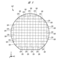
- the wafer WF has a scribe region SR extending in the Y direction and the X direction, and a plurality of chip regions CR (a plurality of die regions) each surrounded by the scribe region SR.
- Each of the plurality of chip regions CR has a rectangular shape in plan view.
- the heaters HT1 and HT2 have a function of selectively changing the temperature of various regions of the wafer WF.
- the heater HT2 is divided into a region HT2a having a circular shape in a plan view, a region HT2b surrounding the outer periphery of the region HT2a in a plan view, and a region HT2c surrounding the outer periphery of the region HT2b in a plan view. It is provided. That is, the region HT2b has a ring shape with an inner diameter and an outer diameter larger than the radius of the region HT2a, and the region HT2c has a ring shape with an inner diameter and an outer diameter larger than the outer diameter of the region HT2b.
- a DC power supply 72 shown in FIG. 3 is electrically connected to each of the regions HT2a to HT2c. Therefore, the control unit C0 can individually control the power supply to the regions HT2a to HT2c. As a result, the temperatures of the regions corresponding to the regions HT2a to HT2c on the wafer WF are individually adjusted.
- the main purpose of the heater HT2 is to make the temperature uniform in the circumferential direction in a plan view, and to control the temperature of the wafer WF according to the reaction product distribution and plasma density distribution during plasma processing. .
- the heater HT1 is provided divided into a plurality of regions HT1d each having a rectangular shape in plan view.
- the plurality of regions HT1d are adjacent to each other in the X direction and the Y direction, and are arranged in a grid pattern.
- a DC power supply 73 shown in FIG. 3 is individually electrically connected to each of the plurality of regions HT1d. Therefore, the control unit C0 can individually control the power supply to the plurality of regions HT1d. Thereby, the temperature of the plurality of chip regions CR is individually adjusted. In other words, a plurality of regions HT1d are provided such that one region HT1d is located below one chip region CR. Therefore, when the power supply to one region HT1d is changed, the temperature of one chip region CR is changed.
- the main purpose of the heater HT1 is to individually adjust the temperature of a plurality of chip regions CR during plasma processing to locally adjust the etching shape. Therefore, while the heater HT2 is divided into three zones (regions HT2a to HT2c), the heater HT1 is divided into, for example, 120 zones. That is, the number of regions HT1d is, for example, 120.
- the heater HT1 there are many power supply lines connecting the plurality of DC power supplies 73 and the plurality of regions HT1d, so there is a problem that the number of regions (cold spots) where the temperature is lower than the set temperature tends to increase locally.
- the temperature of the cold spot can be corrected by Further, although the heater HT2 cannot control the temperature in a fine area, the heater HT1 makes it possible to control the temperature in such a fine area.
- the plasma processing apparatus 1 since the plasma processing apparatus 1 includes the heaters HT1 and HT2, it is possible to improve the uniformity of the temperature within the surface of the wafer WF.
- each of the regions HT2a to HT2c and the plurality of regions HT1d indicates regions that become heaters, and do not indicate the shape of the conductor itself that constitutes the heater.
- each of the regions HT2a to HT2c and the plurality of regions HT1d is configured by a heater wire that is folded back a plurality of times.
- the heater wire is made of a metal material, such as titanium, tungsten, or molybdenum.
- FIG. 9 is a table comparing the characteristics of the heater HT1 and the characteristics of the heater HT2.
- the heat generating area of heater HT2 is larger than that of heater HT1.
- the heater HT1 is divided into a plurality of regions HT1d, the number of power supply lines increases and the amount of current increases. If the amount of current is large and there is contact resistance in the power supply line, there is a risk that damage to the device may occur due to heat generation such as melting loss or thermal deformation. Furthermore, if there are many power supply lines, there is a risk that the power supply lines themselves will generate heat. When such heat-generating locations become crowded, the influence thereof cannot be ignored, and it becomes necessary to take measures to take exhaust heat into consideration within the electrostatic chuck 40. As described above, heater HT1 requires measures to increase the resistance value and decrease the amount of current.
- the area is large and the heater wires laid out are long, so the resistance value tends to be high. Therefore, since the amount of current becomes small, it is necessary to take measures to lower the resistance value.
- the structures of the heater wires forming the heater HT1 (the plurality of regions HT1d) and the heater HT2 (the regions HT2a to HT2c) have the following relationship. Note that here, the material of the heater wire constituting the heater HT1 is the same as the material of the heater wire constituting the heater HT2.
- the thickness of the heater wire constituting the heater HT2 is thicker than the thickness of the heater wire constituting the heater HT1. Further, the line width of the heater wire forming the heater HT2 is wider than the line width of the heater line forming the heater HT1. It is further preferable that both of these relationships are satisfied.
- the power supply is adjusted in consideration of the temperature of each of the regions HT2a to HT2c and the region HT1d and the amount of power supplied to the surrounding area of the corresponding region HT1d.
- the outermost region HT1d of the heater HT1 has an irregular shape. If temperature control is performed with an irregular shape, it is difficult to maintain uniformity at the outermost periphery of the wafer WF. Therefore, temperature variation can be reduced at the outermost peripheral portion of the wafer WF by controlling the temperature using the region HT2c. Furthermore, if it is attempted to form the chip region CR also on the outermost periphery of the wafer WF, that region will have an irregular shape. Therefore, in reality, the outermost peripheral portion of the wafer WF is an area where semiconductor devices are not formed and is not shipped as a product. Therefore, even if the outermost region HT1d of the heater HT1 has an irregular shape and temperature variations occur at the outermost circumferential portion of the wafer WF, there is no significant effect on the manufacturing yield of the wafer WF.
- ⁇ Plasma treatment method> As an example of a plasma processing method, a method of performing an etching process using plasma 3 on a predetermined film formed in advance on the upper surface of a wafer WF will be described below with reference to FIG.
- step S1 DC voltage is supplied from the DC power supplies 72 and 73 to the heaters HT1 and HT2, and the heaters HT1 and HT2 are turned on, according to an instruction from the control unit C0.
- power supply is set to heater HT2 (areas HT2a to HT2c) and heater HT1 (area HT1d) so that the target temperature is reached.
- step S2 the pressure inside the vacuum transfer container connected to the side wall of the vacuum container 2 is reduced to the same pressure as the processing chamber 4.
- the wafer WF is placed on the tip of an arm of a vacuum transfer device such as a robot arm from outside the plasma processing apparatus 1, and is transferred into the vacuum transfer container. By opening the transfer port 11, the wafer WF is transferred from the inside of the vacuum transfer container to the inside of the processing chamber 4 and placed on the sample stage 30. When the arm of the vacuum transfer device leaves the processing chamber 4, the inside of the processing chamber 4 is sealed.
- step S3 a DC voltage is supplied from the DC power supply 71 to the electrode 47, and the wafer WF is held on the upper surface 40t of the electrostatic chuck 40 by the generated electrostatic force.
- a gas having heat transfer properties such as helium (He) is supplied to the gap between the wafer WF and the upper surface 40t of the electrostatic chuck 40 through the hole 61.
- a refrigerant whose temperature has been adjusted to a predetermined temperature by a refrigerant temperature regulator (not shown) is supplied to the refrigerant flow path 51 .
- a refrigerant whose temperature has been adjusted to a predetermined temperature by a refrigerant temperature regulator (not shown) is supplied to the refrigerant flow path 51 .
- step S4 a processing gas whose flow rate and speed are adjusted by a gas supply device (not shown) is supplied to the gap 10 and diffused inside the gap 10.
- the diffused processing gas is supplied above the sample stage 30 through the plurality of holes 9 .
- Processing gas is supplied to the inside of the processing chamber 4, and the inside of the processing chamber 4 is evacuated from the vacuum exhaust port 15. By balancing the two, the pressure inside the processing chamber 4 is adjusted to a value within a range suitable for plasma processing.
- the magnetron oscillator 13 oscillates a microwave electric field.
- the electric field of the microwave propagates inside the waveguide 12 and passes through the window member 7 and the shower plate 8.
- a magnetic field generated by the solenoid coil 14 is supplied to the processing chamber 4 .
- Electron cyclotron resonance (ECR) is generated by the interaction between the magnetic field and the electric field of the microwave.
- plasma 3 is generated inside the processing chamber 4 by excitation, ionization, or dissociation of atoms or molecules of the processing gas.
- step S5 the control unit C0 uses the temperatures detected by the plurality of temperature sensors 52 while performing plasma processing on the wafer WF and the temperatures preset for the plurality of regions HT1d in step S1. Compare the difference with the target temperature. Then, the control unit C0 individually controls the power supply to the plurality of regions HT1d so that the difference becomes small. Here, the control unit C0 individually controls the power supply only to the plurality of regions HT1d without changing the power supply to the regions HT2a to HT2c. Thereby, the temperature of the chip region CR corresponding to the region HT1d whose power supply has been changed is individually adjusted.
- step S6 the target of the etching process shifts to another film. Therefore, the control unit C0 changes the power supply to the regions HT2a to HT2c in order to change the temperature to a temperature suitable for another film.
- the changed temperature is detected by the plurality of temperature sensors 52 and transmitted to the control unit C0.
- the control unit C0 adjusts the power supply to the regions HT2a to HT2c and adjusts the in-plane temperature of the wafer WF so that the error in the changed temperature is within a predetermined temperature range.
- step S5 the same process as step S5 is performed. That is, the power supply to the plurality of regions HT1d is individually controlled, and the temperature of the plurality of chip regions CR is individually adjusted.
- step S7 if there is no need for further etching processing of the wafer WF, the supply of processing gas to the gap 10 is stopped, the transmission of microwaves from the magnetron oscillator 13 is stopped, and the high-frequency power from the high-frequency power source 70 is stopped. Stop supply. This stops plasma processing.
- step S8 static electricity is removed and the adsorption of the wafer WF is released.
- step S9 the arm of the vacuum transfer device enters the inside of the processing chamber 4, and the processed wafer WF is transferred to the outside of the plasma processing device 1.
- Plasma processing device 2 Vacuum container 3
- Plasma 4 Processing chamber 5
- Susceptor ring 6 Conductor ring 7
- Window member 8 Shower plate 9
- Hole 10 Gap 11 Transfer port 12
- Waveguide 13 Magnetron oscillator 14
- Solenoid coil 15 Vacuum exhaust port 16
- Load impedance variable box 17 Load matching device 18
- High frequency power supply 30 Sample stage 40
- Electrostatic chuck 40t Top surface 41 to 45 Dielectric film 46 Shield film 47
- Electrode 50
- Base material Coolant channel 52
- Hole Insulating boss 67
- High frequency Power supply 71 DC power supply 72
- DC power supply 73 DC power supply C0 Control unit
- CR Chip area HT1 Heater HT1d Area HT2 Heater HT2a to HT2c Area
Landscapes
- Engineering & Computer Science (AREA)
- Physics & Mathematics (AREA)
- Microelectronics & Electronic Packaging (AREA)
- General Physics & Mathematics (AREA)
- Manufacturing & Machinery (AREA)
- Computer Hardware Design (AREA)
- Condensed Matter Physics & Semiconductors (AREA)
- Power Engineering (AREA)
- Plasma & Fusion (AREA)
- Chemical & Material Sciences (AREA)
- Analytical Chemistry (AREA)
- Electromagnetism (AREA)
- Spectroscopy & Molecular Physics (AREA)
- Drying Of Semiconductors (AREA)
Priority Applications (5)
| Application Number | Priority Date | Filing Date | Title |
|---|---|---|---|
| KR1020237005509A KR20230135557A (ko) | 2022-03-14 | 2022-03-14 | 플라스마 처리 장치 |
| JP2023511853A JPWO2023175690A1 (ko) | 2022-03-14 | 2022-03-14 | |
| PCT/JP2022/011436 WO2023175690A1 (ja) | 2022-03-14 | 2022-03-14 | プラズマ処理装置 |
| CN202280005615.6A CN117063617A (zh) | 2022-03-14 | 2022-03-14 | 等离子处理装置 |
| TW112105845A TW202336810A (zh) | 2022-03-14 | 2023-02-17 | 電漿處理裝置 |
Applications Claiming Priority (1)
| Application Number | Priority Date | Filing Date | Title |
|---|---|---|---|
| PCT/JP2022/011436 WO2023175690A1 (ja) | 2022-03-14 | 2022-03-14 | プラズマ処理装置 |
Publications (1)
| Publication Number | Publication Date |
|---|---|
| WO2023175690A1 true WO2023175690A1 (ja) | 2023-09-21 |
Family
ID=88022505
Family Applications (1)
| Application Number | Title | Priority Date | Filing Date |
|---|---|---|---|
| PCT/JP2022/011436 WO2023175690A1 (ja) | 2022-03-14 | 2022-03-14 | プラズマ処理装置 |
Country Status (5)
| Country | Link |
|---|---|
| JP (1) | JPWO2023175690A1 (ko) |
| KR (1) | KR20230135557A (ko) |
| CN (1) | CN117063617A (ko) |
| TW (1) | TW202336810A (ko) |
| WO (1) | WO2023175690A1 (ko) |
Citations (4)
| Publication number | Priority date | Publication date | Assignee | Title |
|---|---|---|---|---|
| JP2014150160A (ja) * | 2013-02-01 | 2014-08-21 | Hitachi High-Technologies Corp | プラズマ処理装置および試料台 |
| JP2015515713A (ja) * | 2012-02-28 | 2015-05-28 | ラム リサーチ コーポレーションLam Research Corporation | 半導体処理用の交流駆動を用いる多重ヒータアレイ |
| JP2017028111A (ja) * | 2015-07-23 | 2017-02-02 | 株式会社日立ハイテクノロジーズ | プラズマ処理装置 |
| JP2017157855A (ja) * | 2014-11-20 | 2017-09-07 | 住友大阪セメント株式会社 | 静電チャック装置 |
Family Cites Families (1)
| Publication number | Priority date | Publication date | Assignee | Title |
|---|---|---|---|---|
| JP2007067036A (ja) | 2005-08-30 | 2007-03-15 | Hitachi High-Technologies Corp | 真空処理装置 |
-
2022
- 2022-03-14 JP JP2023511853A patent/JPWO2023175690A1/ja active Pending
- 2022-03-14 KR KR1020237005509A patent/KR20230135557A/ko unknown
- 2022-03-14 WO PCT/JP2022/011436 patent/WO2023175690A1/ja active Application Filing
- 2022-03-14 CN CN202280005615.6A patent/CN117063617A/zh active Pending
-
2023
- 2023-02-17 TW TW112105845A patent/TW202336810A/zh unknown
Patent Citations (4)
| Publication number | Priority date | Publication date | Assignee | Title |
|---|---|---|---|---|
| JP2015515713A (ja) * | 2012-02-28 | 2015-05-28 | ラム リサーチ コーポレーションLam Research Corporation | 半導体処理用の交流駆動を用いる多重ヒータアレイ |
| JP2014150160A (ja) * | 2013-02-01 | 2014-08-21 | Hitachi High-Technologies Corp | プラズマ処理装置および試料台 |
| JP2017157855A (ja) * | 2014-11-20 | 2017-09-07 | 住友大阪セメント株式会社 | 静電チャック装置 |
| JP2017028111A (ja) * | 2015-07-23 | 2017-02-02 | 株式会社日立ハイテクノロジーズ | プラズマ処理装置 |
Also Published As
| Publication number | Publication date |
|---|---|
| KR20230135557A (ko) | 2023-09-25 |
| JPWO2023175690A1 (ko) | 2023-09-21 |
| TW202336810A (zh) | 2023-09-16 |
| CN117063617A (zh) | 2023-11-14 |
Similar Documents
| Publication | Publication Date | Title |
|---|---|---|
| CN108281342B (zh) | 等离子体处理装置 | |
| WO2019032787A1 (en) | DISTRIBUTED ELECTRODE NETWORK FOR PLASMA PROCESSING | |
| TWI762551B (zh) | 電漿處理裝置 | |
| JP3150058B2 (ja) | プラズマ処理装置及びプラズマ処理方法 | |
| JP7364758B2 (ja) | プラズマ処理方法 | |
| JP2013526778A (ja) | 限定プロセス容積pecvdチャンバ | |
| JP2015162266A (ja) | プラズマ処理装置 | |
| US20160118284A1 (en) | Plasma processing apparatus | |
| JP2019140155A (ja) | プラズマ処理装置 | |
| JP2020113618A (ja) | 誘導結合プラズマ処理装置 | |
| TW201929031A (zh) | 製程中之超侷域化電漿與均勻性控制 | |
| JP3814176B2 (ja) | プラズマ処理装置 | |
| TWI723406B (zh) | 電漿處理裝置 | |
| WO2023175690A1 (ja) | プラズマ処理装置 | |
| TWI738309B (zh) | 電漿處理裝置 | |
| JP2001210628A (ja) | プラズマ処理装置 | |
| WO2023248406A1 (ja) | プラズマ処理装置 | |
| JP2002190473A (ja) | プラズマ処理装置 | |
| WO2022201351A1 (ja) | プラズマ処理装置およびプラズマ処理方法 | |
| KR20240022756A (ko) | 척 온도 제어 유닛 및 이를 포함하는 기판 처리 장치 | |
| JP2021192425A (ja) | プラズマ処理装置 | |
| JP2019160714A (ja) | プラズマ処理装置 |
Legal Events
| Date | Code | Title | Description |
|---|---|---|---|
| WWE | Wipo information: entry into national phase |
Ref document number: 2023511853 Country of ref document: JP |
|
| WWE | Wipo information: entry into national phase |
Ref document number: 202280005615.6 Country of ref document: CN |
|
| WWE | Wipo information: entry into national phase |
Ref document number: 18025018 Country of ref document: US |
|
| 121 | Ep: the epo has been informed by wipo that ep was designated in this application |
Ref document number: 22931975 Country of ref document: EP Kind code of ref document: A1 |