WO2023166898A1 - 金属材料の表面検査方法、金属材料の表面検査装置、及び金属材料 - Google Patents
金属材料の表面検査方法、金属材料の表面検査装置、及び金属材料 Download PDFInfo
- Publication number
- WO2023166898A1 WO2023166898A1 PCT/JP2023/003026 JP2023003026W WO2023166898A1 WO 2023166898 A1 WO2023166898 A1 WO 2023166898A1 JP 2023003026 W JP2023003026 W JP 2023003026W WO 2023166898 A1 WO2023166898 A1 WO 2023166898A1
- Authority
- WO
- WIPO (PCT)
- Prior art keywords
- metal material
- light
- surface inspection
- images
- image
- Prior art date
- Legal status (The legal status is an assumption and is not a legal conclusion. Google has not performed a legal analysis and makes no representation as to the accuracy of the status listed.)
- Ceased
Links
Images


Classifications
-
- G—PHYSICS
- G01—MEASURING; TESTING
- G01N—INVESTIGATING OR ANALYSING MATERIALS BY DETERMINING THEIR CHEMICAL OR PHYSICAL PROPERTIES
- G01N21/00—Investigating or analysing materials by the use of optical means, i.e. using sub-millimetre waves, infrared, visible or ultraviolet light
- G01N21/84—Systems specially adapted for particular applications
- G01N21/88—Investigating the presence of flaws or contamination
- G01N21/89—Investigating the presence of flaws or contamination in moving material, e.g. running paper or textiles
- G01N21/892—Investigating the presence of flaws or contamination in moving material, e.g. running paper or textiles characterised by the flaw, defect or object feature examined
-
- G—PHYSICS
- G01—MEASURING; TESTING
- G01N—INVESTIGATING OR ANALYSING MATERIALS BY DETERMINING THEIR CHEMICAL OR PHYSICAL PROPERTIES
- G01N21/00—Investigating or analysing materials by the use of optical means, i.e. using sub-millimetre waves, infrared, visible or ultraviolet light
- G01N21/84—Systems specially adapted for particular applications
- G01N21/88—Investigating the presence of flaws or contamination
- G01N21/8806—Specially adapted optical and illumination features
-
- G—PHYSICS
- G01—MEASURING; TESTING
- G01N—INVESTIGATING OR ANALYSING MATERIALS BY DETERMINING THEIR CHEMICAL OR PHYSICAL PROPERTIES
- G01N21/00—Investigating or analysing materials by the use of optical means, i.e. using sub-millimetre waves, infrared, visible or ultraviolet light
- G01N21/17—Systems in which incident light is modified in accordance with the properties of the material investigated
- G01N21/25—Colour; Spectral properties, i.e. comparison of effect of material on the light at two or more different wavelengths or wavelength bands
-
- G—PHYSICS
- G01—MEASURING; TESTING
- G01N—INVESTIGATING OR ANALYSING MATERIALS BY DETERMINING THEIR CHEMICAL OR PHYSICAL PROPERTIES
- G01N21/00—Investigating or analysing materials by the use of optical means, i.e. using sub-millimetre waves, infrared, visible or ultraviolet light
- G01N21/17—Systems in which incident light is modified in accordance with the properties of the material investigated
- G01N21/25—Colour; Spectral properties, i.e. comparison of effect of material on the light at two or more different wavelengths or wavelength bands
- G01N21/31—Investigating relative effect of material at wavelengths characteristic of specific elements or molecules, e.g. atomic absorption spectrometry
-
- G—PHYSICS
- G01—MEASURING; TESTING
- G01N—INVESTIGATING OR ANALYSING MATERIALS BY DETERMINING THEIR CHEMICAL OR PHYSICAL PROPERTIES
- G01N21/00—Investigating or analysing materials by the use of optical means, i.e. using sub-millimetre waves, infrared, visible or ultraviolet light
- G01N21/84—Systems specially adapted for particular applications
- G01N21/88—Investigating the presence of flaws or contamination
- G01N21/8851—Scan or image signal processing specially adapted therefor, e.g. for scan signal adjustment, for detecting different kinds of defects, for compensating for structures, markings, edges
-
- G—PHYSICS
- G01—MEASURING; TESTING
- G01N—INVESTIGATING OR ANALYSING MATERIALS BY DETERMINING THEIR CHEMICAL OR PHYSICAL PROPERTIES
- G01N21/00—Investigating or analysing materials by the use of optical means, i.e. using sub-millimetre waves, infrared, visible or ultraviolet light
- G01N21/84—Systems specially adapted for particular applications
- G01N21/88—Investigating the presence of flaws or contamination
- G01N21/89—Investigating the presence of flaws or contamination in moving material, e.g. running paper or textiles
- G01N21/8914—Investigating the presence of flaws or contamination in moving material, e.g. running paper or textiles characterised by the material examined
-
- G—PHYSICS
- G01—MEASURING; TESTING
- G01N—INVESTIGATING OR ANALYSING MATERIALS BY DETERMINING THEIR CHEMICAL OR PHYSICAL PROPERTIES
- G01N33/00—Investigating or analysing materials by specific methods not covered by groups G01N1/00 - G01N31/00
- G01N33/20—Metals
- G01N33/204—Structure thereof, e.g. crystal structure
- G01N33/2045—Defects
-
- G—PHYSICS
- G06—COMPUTING OR CALCULATING; COUNTING
- G06N—COMPUTING ARRANGEMENTS BASED ON SPECIFIC COMPUTATIONAL MODELS
- G06N20/00—Machine learning
-
- G—PHYSICS
- G01—MEASURING; TESTING
- G01N—INVESTIGATING OR ANALYSING MATERIALS BY DETERMINING THEIR CHEMICAL OR PHYSICAL PROPERTIES
- G01N21/00—Investigating or analysing materials by the use of optical means, i.e. using sub-millimetre waves, infrared, visible or ultraviolet light
- G01N21/84—Systems specially adapted for particular applications
- G01N21/88—Investigating the presence of flaws or contamination
- G01N21/8806—Specially adapted optical and illumination features
- G01N2021/8845—Multiple wavelengths of illumination or detection
-
- G—PHYSICS
- G01—MEASURING; TESTING
- G01N—INVESTIGATING OR ANALYSING MATERIALS BY DETERMINING THEIR CHEMICAL OR PHYSICAL PROPERTIES
- G01N21/00—Investigating or analysing materials by the use of optical means, i.e. using sub-millimetre waves, infrared, visible or ultraviolet light
- G01N21/84—Systems specially adapted for particular applications
- G01N21/88—Investigating the presence of flaws or contamination
- G01N21/8851—Scan or image signal processing specially adapted therefor, e.g. for scan signal adjustment, for detecting different kinds of defects, for compensating for structures, markings, edges
- G01N2021/8854—Grading and classifying of flaws
- G01N2021/8858—Flaw counting
-
- G—PHYSICS
- G01—MEASURING; TESTING
- G01N—INVESTIGATING OR ANALYSING MATERIALS BY DETERMINING THEIR CHEMICAL OR PHYSICAL PROPERTIES
- G01N21/00—Investigating or analysing materials by the use of optical means, i.e. using sub-millimetre waves, infrared, visible or ultraviolet light
- G01N21/84—Systems specially adapted for particular applications
- G01N21/88—Investigating the presence of flaws or contamination
- G01N21/89—Investigating the presence of flaws or contamination in moving material, e.g. running paper or textiles
- G01N21/8914—Investigating the presence of flaws or contamination in moving material, e.g. running paper or textiles characterised by the material examined
- G01N2021/8918—Metal
Definitions
- the present invention relates to a metal material surface inspection method, a metal material surface inspection apparatus, and a metal material that optically detect surface defects in the metal material.
- the steel materials referred to here refer to steel products such as seamless steel pipes, welded steel pipes, hot-rolled steel plates, cold-rolled steel plates, thick plates, and shaped steel, as well as the steel products produced in the process of manufacturing these steel products.
- Semi-finished products such as slabs.
- a method for detecting surface defects in steel materials a method has been proposed in which a billet in the manufacturing process of seamless steel pipes is irradiated with light, the reflected light is received, and the presence or absence of surface defects is determined based on the amount of reflected light. (See Patent Document 1).
- visible light in multiple wavelength ranges that do not affect each other and do not affect each other with the self-luminescence emitted from the hot work steel are directed obliquely symmetrically with respect to the normal to the surface of the hot work steel.
- a method has also been proposed for detecting surface defects in hot-work steel materials by irradiating light from the surface of the hot-work steel material, obtaining an image of the combined reflected light and an image of the individual reflected light in the normal direction of the surface of the hot-work steel material, and combining these images. (See Patent Document 2).
- the present invention has been made in view of the above problems, and its object is to provide a surface inspection method and a surface inspection apparatus for metal materials that can accurately detect surface defects of metal materials without omission. Another object of the present invention is to provide a high-quality metal material free from surface defects.
- a metal material surface inspection method is a metal material surface inspection method for optically detecting surface defects of a metal material, comprising: an irradiation step of irradiating a surface of the metal material with light; an imaging step of obtaining a plurality of images by imaging light reflected from the surface of the metal material by the light irradiated in the irradiation step in two or more different wavelength bands; a detecting step of detecting surface defects existing on the surface of the metal material from information of relative signal intensity between the plurality of images obtained from the positions.
- the detection step includes a step of detecting the surface defect using a determiner created by a machine learning technique using relative intensities between the plurality of images or a plurality of quantities calculated from the relative intensities as feature quantities. good.
- the irradiation step includes the step of irradiating the light so that the angle with respect to the normal direction of the surface of the metal material is within the range of 60 ° or more and less than 90 °
- the imaging step includes the step of irradiating the light with respect to the surface of the metal material It is preferable to include the step of receiving the reflected light so that the light receiving angle is in the range of 0° or more and less than 20°.
- At least one of the two or more different wavelength bands is preferably a wavelength band of 500 nm or less.
- At least one of the two or more different wavelength bands is preferably a wavelength band of 650 nm or more.
- a metal material surface inspection apparatus is a metal material surface inspection apparatus for optically detecting surface defects of a metal material, comprising: irradiation means for irradiating a surface of the metal material with light; imaging means for obtaining a plurality of images by imaging light reflected from the surface of the metal material by the light irradiated by the irradiation means in two or more different wavelength bands; a detecting means for detecting surface defects existing on the surface of the metal material from information of relative signal intensity between the plurality of images obtained from the positions.
- the surface properties of the metal material according to the present invention are guaranteed using the method for inspecting the surface of the metal material according to the present invention.
- the surface inspection method and surface inspection apparatus for metallic materials it is possible to accurately detect surface defects in metallic materials without omission. Moreover, according to the metal material of the present invention, it is possible to provide a high-quality metal material free from surface defects.
- FIG. 1 is a diagram showing an example of pattern-like defects and harmless patterns.
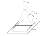
- FIG. 2 is a schematic diagram showing the configuration of the device used in the test.
- FIG. 3 is a diagram showing the result of comparing the relationship between the signal intensity and the wavelength of the pattern-like defective portion and the healthy portion.
- FIG. 4 is a diagram showing the results of comparing the relationship between the incident angle of the illumination light, the signal intensity difference between the pattern-like defect portion and the sound portion, and the wavelength.
- FIG. 5 is a schematic diagram showing the configuration of the surface inspection apparatus for metal materials according to the first embodiment of the present invention.
- FIG. 6 is a schematic diagram showing the configuration of a surface inspection apparatus for metal materials according to a second embodiment of the present invention.
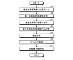
- FIG. 7 is a flow chart showing the flow of surface inspection processing, which is one embodiment of the present invention.
- FIG. 8 is a diagram showing an example of a difference image.
- FIG. 9 is a diagram showing an example of a difference image.
- a thick steel plate which is a type of steel product, is covered with an oxide film called black scale on the surface, and a pattern called harmless pattern, which does not affect the quality of the steel product, may occur.
- pattern defects such as scabs occur on the surface of thick steel plates, but as shown in FIG. 1, it is difficult to distinguish between pattern defects and harmless patterns based on the difference in brightness. Therefore, the inventors of the present invention have focused on the fact that minute red scales (Fe 2 O 3 ) are likely to be generated on the pattern-like defects, and the red scales make the pattern-like defects look reddish.
- a test was conducted to detect pattern defects using the characteristics.
- Fig. 2 shows the configuration of the device used for the test. As shown in FIG.
- a thick steel plate sample SA having pattern defects was placed on a linear stage 1, and illumination light L having a broadband wavelength from a xenon light source 2 was applied to the surface of the thick steel plate sample SA.
- a spectroscopic image of each wavelength was taken using a spectroscopic camera 3 having a one-dimensional field of view.
- Fig. 3 shows the result of comparing the relationship between the signal intensity and the wavelength of the pattern-like defect part and the healthy part using the spectroscopic image.
- the signal intensity characteristics on the short wavelength side and the long wavelength side are relatively different between the pattern-like defect portion and the sound portion. This suggests that pattern-like defects, which were difficult to detect by harmless pattern signals at a single wavelength alone, may be detectable by comparing signal intensities between wavelengths. Therefore, the spectral image of the 415 nm wavelength band (415 nm image) and the spectral image of the 750 nm wavelength band (750 nm image) are subjected to luminance correction so that the average value of luminance is constant.
- FIG. 8 shows an image obtained by taking the difference in luminance value. As shown in FIG. 8, the signal of the harmless pattern is canceled by the difference, and the signal of the pattern-like defect is emphasized.
- FIG. 4 shows the results of comparing the incident angle of the illumination light L (the angle with respect to the surface normal vector of the steel plate), the signal intensity difference between the pattern-like defect portion and the sound portion, and the wavelength. Incident angles are described as 20°, 30°, etc. in the legend of FIG. As shown in FIG. 4, as the incident angle of the illumination light L increases, the signal intensity difference between the short wavelength side and the long wavelength side increases. Therefore, the incident angle of the illumination light L should be increased in order to efficiently detect the spectral reflection characteristics of the object, that is, the color difference.
- the pattern-like defect of a thick steel plate has been described, but the present invention can be applied to the detection of a surface defect having a spectral reflection characteristic different from that of a sound portion occurring on the surface of other metal materials.
- FIG. 5 A surface inspection apparatus for metal materials, which is one embodiment of the present invention, conceived from the above technical idea, will be described below with reference to FIGS. 5 to 8.
- FIG. 5 A surface inspection apparatus for metal materials, which is one embodiment of the present invention, conceived from the above technical idea, will be described below with reference to FIGS. 5 to 8.
- FIG. 5 A surface inspection apparatus for metal materials, which is one embodiment of the present invention, conceived from the above technical idea, will be described below with reference to FIGS. 5 to 8.
- FIG. 5 is a schematic diagram showing the configuration of the surface inspection apparatus for metal materials according to the first embodiment of the present invention.
- a metal material surface inspection apparatus 10 according to a first embodiment of the present invention is an apparatus for detecting surface defects in a plate-shaped steel material S conveyed in the direction of the arrow in the drawing.
- a metal material surface inspection apparatus 10 according to the first embodiment of the present invention includes a light source 11, an encoder and pulse generator 12, an area sensor 13 capable of capturing spectral images in a plurality of wavelength bands, an image processing device 14, and A monitor 15 is provided as a main component.
- the light source 11 irradiates the inspection target portion on the surface of the steel material S with the illumination light L according to the trigger signal output by the pulse generator every time the pulse signal is transmitted from the encoder a certain number of times.
- the light source 11 is preferably arranged so that the irradiation direction of the illumination light L is inclined within a range of 60° or more and less than 90° with respect to the normal line direction of the steel material S surface. As a result, surface defects can be accurately detected from the difference image.
- a plurality of light sources 11 may be arranged.
- a xenon light source is used as the light source 11.
- the light source 11 includes components of a plurality of different wavelength bands
- a light source with broadband characteristics such as a metal halide light source, a halogen light source, a mercury lamp, and an incandescent lamp may be used.
- the light sources may also be a combination of light sources with specific narrowband characteristics such as LEDs or lasers.
- a flash light source or pulse lighting may be used to prevent image blurring.
- the area sensor 13 captures spectral images of a plurality of different wavelength bands at approximately the same position of the steel material S.
- a plurality of captured spectral images are preferably coaxial, but may be aligned by image processing.
- a filter that transmits different wavelength bands is attached to each element so as to be nested, and a Bayer method that generates a plurality of images later or a prism and a plurality of elements are used to adjust so that they are coaxial. Prism type.
- the wavelength band for receiving light may be narrow band with a wavelength selection filter or the like if there is a margin in the amount of light.
- at least one of a plurality of different wavelength bands should include a narrow wavelength band of 650 nm or more, and at least one should include a narrow wavelength band of 500 nm or less.
- the area sensor 13 captures a spectroscopic image in synchronization with the light source 11 according to the trigger signal output from the pulse generator. Except for the spectral image in which the edge of the steel material S is photographed, it is assumed that the luminance value of each channel of the spectral image is not saturated.
- two-channel area sensors that capture light in long and short wavelength bands are used, but the apparatus may be configured to image three or more wavelength bands with three or more channels of area sensors.
- the area sensor 13 preferably receives the reflected light so that the light-receiving angle with respect to the normal direction of the surface of the steel material S is in the range of 0° or more and less than 20°.
- the image processing device 14 detects surface defects in the inspected portion by performing differential processing, which will be described later, between spectral images input from each channel of the area sensor 13 . Then, the image processing device 14 outputs to the monitor 15 the spectral image input from the area sensor 13 , the spectral image after differential processing, and information on the surface defect detection result.
- FIG. 6 is a schematic diagram showing the configuration of a surface inspection apparatus for metal materials according to a second embodiment of the present invention.
- a metal material surface inspection apparatus 20 according to a second embodiment of the present invention detects surface defects in a plate-shaped steel material S conveyed in the direction of the arrow in the figure.
- the difference from the metal material surface inspection apparatus 10 of the first embodiment is that the light source 11 is a line light source 21 and the area sensor 13 is a line sensor 22 .
- the line sensor 22 By using the line sensor 22, the field of view becomes only one line, and compared with the first embodiment, there is an advantage that the optical conditions are stable. Disadvantages such as vulnerability to positional fluctuations also exist.
- the metal material surface inspection apparatuses 10 and 20 having such a configuration perform the following surface inspection processing, thereby distinguishing pattern-like defective portions from healthy portions having harmless patterns in the inspected portion.
- the pattern-like defect described here is a defect that does not appear to have unevenness from the surface, such as a foreign matter being pressed or scale being formed on a concave defect.
- the healthy portion with harmless patterns means a portion having a surface film or surface properties different in optical characteristics from the base iron portion with a thickness of several to several tens of ⁇ m, such as black scale, and is inspected for surface inspection. This is the part that causes noise in processing.
- FIG. 7 is a flow chart showing the flow of surface inspection processing, which is one embodiment of the present invention.
- the surface inspection process shown in FIG. 7 starts at the timing when a command to execute the surface inspection process is input to the image processing device 14, and the surface inspection process proceeds to the process of step S1.
- step S1 the image processing device 14 performs alignment processing when the positions of the spectral images of a plurality of different wavelength bands are shifted pixel by pixel. If spectral images cannot be captured coaxially, it is necessary to align the spectral images of different wavelength bands.
- the alignment method changes depending on the form of the positional deviation of the spectral images of each wavelength band, and it is preferable to perform processing such as translation, linear conversion, and one-to-one correspondence between pixels as necessary. Thereby, the process of step S1 is completed, and the surface inspection process proceeds to the process of step S2.
- step S2 the image processing device 14 performs first preprocessing such as correction to keep the average brightness constant for a plurality of spectral images of different wavelength bands, brightness unevenness correction, signal intensity normalization processing, and the like. to run. Thereby, the process of step S2 is completed, and the surface inspection process proceeds to the process of step S3.
- first preprocessing such as correction to keep the average brightness constant for a plurality of spectral images of different wavelength bands, brightness unevenness correction, signal intensity normalization processing, and the like.
- the image processing device 14 compares a plurality of spectral images in different wavelength bands, and generates a composite processed image that emphasizes only pattern defects by utilizing differences in spectral reflection characteristics. Specifically, the image processing device 14 selects two spectral images having a large difference in spectral reflectance characteristics, and calculates the luminance difference, ratio, etc., between the two spectral images to generate a synthetic processed image. . A case will be described in which a difference image between two spectral images is generated as a synthesized processed image.
- the image processing device 14 calculates the luminance value of the first spectral image Ib (for example, the luminance value of the first channel having sensitivity characteristics corresponding to the wavelength band on the short wavelength side) as shown in the following formula (1). ) by subtracting the luminance value of the second spectral image Ir (for example, the luminance value of the second channel having sensitivity characteristics corresponding to the wavelength band on the long wavelength side) Ir (x, y) from Ib (x, y) A luminance value Id1 (x, y) of the difference image Id1 is calculated.
- the luminance value of the first spectral image Ib for example, the luminance value of the first channel having sensitivity characteristics corresponding to the wavelength band on the short wavelength side
- the spectral images Ib and Ir are images with the number of pixels X ⁇ Y. Further, in the xy coordinate system of two orthogonal axes set for each of the spectral images Ib and Ir, the x coordinate is 1 ⁇ x ⁇ X and the y coordinate is 1 ⁇ y ⁇ Y. Further, in this example, a difference image is generated as a composite processed image, but an image having a ratio of luminance values using Equation (2) shown below may be generated as a composite processed image. Alternatively, the luminance values of the two spectral images may be threshold-processed separately, and then AND-processed to generate a composite processed image.
- step S3 is completed, and the surface inspection process proceeds to the process of step S4.
- (a) Space conversion method This method is effective for three-channel, particularly color images, and is a method for generating an image that extracts the influence of spectral reflection characteristics (color) by converting the color space.
- Color spaces after conversion include an HSV space and an HLS space, and information on spectral reflection characteristics appears in hue information in each of them.
- threshold processing may be performed on the luminance value of each color image after conversion to XYZ, L*u*v*, and L*a*b* spaces and normalizing the luminance component.
- Statistical Multivariate Analysis Method This is a method of extracting portions having different spectral reflectance characteristics by statistical multivariate analysis, using the luminance values of each wavelength band of each pixel as feature amount vectors.
- PCA principal component analysis
- the Mahalanobis distance of each pixel is the representative of that pixel. Reconstruct the image as values. Since the pattern-like defect portion has a different color tone, it is expected that the Mahalanobis distance is larger than that of the healthy portion.
- principal component analysis has been described here, the same effect can be obtained by similarly calculating the degree of divergence from the model using a Gaussian mixture model, independent component analysis, or regression model.
- (c) Machine learning method The method is the same as the statistical multivariate analysis method up to the point where the luminance value of each wavelength band of each pixel is used as a feature vector. is supervised, and a judging machine is created by general supervised learning to judge whether each pixel is a pattern-like defective portion or a normal portion.
- k-means kernel method, decision tree method, Gaussian mixture model, regression model, or the like may be used.
- this method is used, the threshold processing described later is not necessary, and pixels that are defect candidates can be directly extracted.
- step S4 the image processing device 14 generates an image in which surface defects are emphasized by performing second preprocessing using a frequency filter or the like on the composite processed image. Thereby, the process of step S4 is completed, and the surface inspection process proceeds to the process of step S5.
- step S5 the image processing device 14 generates a binarized image by performing threshold processing on the luminance values of the image obtained by the process of step S4. Thereby, the process of step S5 is completed, and the surface inspection process proceeds to the process of step S6.
- step S6 the image processing device 14 performs connected/isolated point removal on the binarized image by processing such as expansion/contraction processing as necessary, and then considers adjacent pixels as blobs. A labeling process is performed to label the Then, the image processing device 14 uses the blob extracted by the labeling process as a surface defect candidate portion. Thereby, the process of step S6 is completed, and the surface inspection process proceeds to the process of step S7.
- the image processing device 14 determines the type and grade of the surface defect (including harmless) for each surface defect candidate portion obtained by the process of step S6.
- Judgment methods can be manually defined judgment rules, regression models (linear regression, logistic regression, multiple regression, support vector machines, nonlinear kernels, etc.), decision tree models, random forests, Bayesian estimation models, mixed Gaussian models, These models may be automatically generated by a general machine learning method using feature quantities such as a boosting method. In this case, by adding each representative value (average/maximum) of the luminance values of multiple spectral images and values (sum/difference/ratio) with which each representative value can be compared to the feature quantity, the spectral reflectance characteristics can be calculated.
- a convolutional neural network may also be used if enough N numbers of data are obtained. Also, a plurality of machine learning techniques may be combined. The determination result is displayed on the monitor 15 and used for guidance, or is collected by the server and used for determining whether the steel material S can be shipped and whether maintenance is necessary. As a result, the processing of step S7 is completed, and a series of surface inspection processing ends.
- the surface of the steel material S is irradiated with light, and two reflected light beams from the surface of the steel material S due to the irradiated light are obtained. Images are taken in different wavelength bands as described above, and surface defects present on the surface of the steel material S are detected from information on relative signal intensities between a plurality of images obtained from the same position on the surface of the steel material S. As a result, the surface defects of the steel material S can be accurately detected without omission.
- the presence or absence of surface defects in a metal material such as steel S is investigated using the surface inspection process, which is one embodiment of the present invention, and the occurrence of surface defects (incidence rate, defect size, etc.) is determined to a predetermined allowable level. Carry out quality assurance to confirm whether the product is substandard. This makes it possible to provide a metal material with guaranteed surface properties. In practice, quality can be guaranteed by stating, for example, whether or not surface defects are below a predetermined allowable standard in a statement of delivery or an inspection certificate.
- Example 1 As Example 1, an example of detecting surface defects in a thick steel plate using the present invention will be shown.
- the surface defects are in the form of pressure bonding to the steel plate surface during the manufacturing process of the steel plate, and when viewed from the steel plate surface, there are no uneven portions.
- FIG. 8 shows a difference image obtained by taking a spectral image in a wavelength band of 415 nm and a spectral image in a wavelength band of 750 nm for a surface defect of a steel plate, performing brightness correction so that the average value is constant, and taking the difference. Signals of harmless patterns such as black scales are canceled by the difference, and only signals of pattern-like defects are emphasized.
- the characteristics of the spectral reflectance spectra of the surface defective portion and the normal portion are utilized to generate a spectral image obtained by capturing the light on the long wavelength side and the spectral image on the short wavelength side. It was confirmed that defects can be detected with high accuracy.
- surface layer scale having a surface reflection spectrum similar to that of the surface defect portion may be generated in the sound portion. By discriminating the surface defects, it is possible to suppress over-detection and detect surface defects with high accuracy.
- Example 2 As Example 2, an example in which the present invention is used to detect the red scale of a steel plate is shown. On the surface of the thick steel plate, red scales, black scales, and base iron portions where the scales are peeled off are unevenly present.
- the scale of hot-manufactured steel materials becomes layered as oxidation progresses , and is composed of wustite (FeO), magnetite ( Fe3O4 ), and hematite ( Fe2O3 ) in the order closest to the base iron . There are many.
- the scale on the surface is mainly composed of wustite or magnetite, it becomes a black scale, and tends to be a uniform scale that has high mechanical strength and is difficult to peel off.
- red scale tends to be avoided because it easily peels off and adheres to factory equipment and stains it, as well as causing unevenness in the color tone of the final product.
- brightness correction was performed so that the average value of the brightness of the R component and B component images was constant, and the difference between the R component image and the B component image was calculated. The images taken are shown in FIGS. 9(a) and 9(b).
- the camera elements and filters were designed so that the R channel could capture images in a narrow wavelength band of 650 nm or more, and the B channel could capture images in a narrow wavelength band of 500 nm or less.
- the signals of the black scale and the base iron portion are canceled by the difference, and only the signal of the red scale is emphasized.
- a two-dimensional image obtained by capturing light on the long wavelength side and a two-dimensional image captured by capturing light on the short wavelength side by utilizing the characteristics of the spectral reflection spectra of the red scale and the black scale. It was confirmed that the red scale can be detected with high accuracy by creating a differential image.
- quality assurance is performed by calculating the ratio and degree of the red scale generation area to the entire surface of the steel plate, and the distribution of red scale generation is used for temperature control in the rolling process and for detecting abnormalities in descaling equipment. can be
- the present invention it is possible to provide a surface inspection method and a surface inspection apparatus for metal materials that can accurately detect surface defects in metal materials without omission. Moreover, according to the present invention, it is possible to provide a high-quality metal material free from surface defects.
Landscapes
- Physics & Mathematics (AREA)
- Chemical & Material Sciences (AREA)
- General Physics & Mathematics (AREA)
- Engineering & Computer Science (AREA)
- Life Sciences & Earth Sciences (AREA)
- Health & Medical Sciences (AREA)
- Biochemistry (AREA)
- General Health & Medical Sciences (AREA)
- Immunology (AREA)
- Pathology (AREA)
- Analytical Chemistry (AREA)
- Theoretical Computer Science (AREA)
- Software Systems (AREA)
- Computer Vision & Pattern Recognition (AREA)
- Spectroscopy & Molecular Physics (AREA)
- Textile Engineering (AREA)
- Computing Systems (AREA)
- Data Mining & Analysis (AREA)
- Evolutionary Computation (AREA)
- Medical Informatics (AREA)
- Artificial Intelligence (AREA)
- General Engineering & Computer Science (AREA)
- Mathematical Physics (AREA)
- Medicinal Chemistry (AREA)
- Food Science & Technology (AREA)
- Signal Processing (AREA)
- Crystallography & Structural Chemistry (AREA)
- Investigating Materials By The Use Of Optical Means Adapted For Particular Applications (AREA)
Priority Applications (6)
| Application Number | Priority Date | Filing Date | Title |
|---|---|---|---|
| EP23763160.1A EP4443143A4 (en) | 2022-03-03 | 2023-01-31 | Surface testing method for metallic material, surface testing device for metallic material and metallic material |
| US18/729,440 US20250116609A1 (en) | 2022-03-03 | 2023-01-31 | Surface inspection method for metal material, surface inspection apparatus for metal material, and metal material |
| CN202380018899.7A CN118591726A (zh) | 2022-03-03 | 2023-01-31 | 金属材料的表面检查方法、金属材料的表面检查装置和金属材料 |
| KR1020247025500A KR20240129014A (ko) | 2022-03-03 | 2023-01-31 | 금속 재료의 표면 검사 방법, 금속 재료의 표면 검사 장치 및, 금속 재료 |
| JP2023528049A JP7741179B2 (ja) | 2022-03-03 | 2023-01-31 | 鋼材の表面検査方法及び表面検査装置 |
| JP2025113885A JP2025135005A (ja) | 2022-03-03 | 2025-07-04 | 鋼材の表面検査方法及び表面検査装置 |
Applications Claiming Priority (2)
| Application Number | Priority Date | Filing Date | Title |
|---|---|---|---|
| JP2022-032278 | 2022-03-03 | ||
| JP2022032278 | 2022-03-03 |
Publications (1)
| Publication Number | Publication Date |
|---|---|
| WO2023166898A1 true WO2023166898A1 (ja) | 2023-09-07 |
Family
ID=87883270
Family Applications (1)
| Application Number | Title | Priority Date | Filing Date |
|---|---|---|---|
| PCT/JP2023/003026 Ceased WO2023166898A1 (ja) | 2022-03-03 | 2023-01-31 | 金属材料の表面検査方法、金属材料の表面検査装置、及び金属材料 |
Country Status (7)
| Country | Link |
|---|---|
| US (1) | US20250116609A1 (https=) |
| EP (1) | EP4443143A4 (https=) |
| JP (2) | JP7741179B2 (https=) |
| KR (1) | KR20240129014A (https=) |
| CN (1) | CN118591726A (https=) |
| TW (1) | TWI849729B (https=) |
| WO (1) | WO2023166898A1 (https=) |
Cited By (1)
| Publication number | Priority date | Publication date | Assignee | Title |
|---|---|---|---|---|
| US12621577B2 (en) * | 2021-12-03 | 2026-05-05 | Canon Kabushiki Kaisha | Apparatus, optical apparatus, image pickup method, and non-transitory computer-readable storage medium for correcting aberration and density unevenness among a plurality of images |
Families Citing this family (2)
| Publication number | Priority date | Publication date | Assignee | Title |
|---|---|---|---|---|
| CN119131014B (zh) * | 2024-11-08 | 2025-03-14 | 宁德时代新能源科技股份有限公司 | 图像处理方法、缺陷检测方法及相关装置和存储介质 |
| KR102880634B1 (ko) * | 2024-12-17 | 2025-11-04 | (주)피앤씨네트워크 | 철강 금속표면 Shear Line 자동화 공정을 위한 지능형시스템 |
Citations (10)
| Publication number | Priority date | Publication date | Assignee | Title |
|---|---|---|---|---|
| JPS5952735A (ja) | 1982-09-20 | 1984-03-27 | Kawasaki Steel Corp | 熱間鋼片の表面欠陥検出方法 |
| JPH0431753A (ja) * | 1990-05-28 | 1992-02-03 | Dainippon Printing Co Ltd | 異物検査装置 |
| JPH04113260A (ja) * | 1990-09-03 | 1992-04-14 | Nkk Corp | 表面欠陥の検出方法及び装置 |
| JPH1137949A (ja) | 1997-07-22 | 1999-02-12 | Sumitomo Metal Ind Ltd | 表面疵検知方法及び装置 |
| JPH11337502A (ja) * | 1998-05-25 | 1999-12-10 | Kobe Steel Ltd | 圧延材の表面欠陥検出方法および装置 |
| JP2010266430A (ja) * | 2009-04-15 | 2010-11-25 | Jfe Steel Corp | 鋼板表面欠陥検査方法および装置 |
| JP2011191252A (ja) * | 2010-03-16 | 2011-09-29 | Nippon Steel Engineering Co Ltd | 金属の表面品質評価方法および金属の表面品質評価装置 |
| WO2013012106A1 (ko) * | 2011-07-18 | 2013-01-24 | 동국대학교 경주캠퍼스 산학협력단 | 금속 표면 결함 검출을 위한 카메라, 카메라를 포함하는 금속 표면 결함 검출 장치, 및 금속 표면 결함 검출 방법 |
| JP6079948B1 (ja) | 2015-06-25 | 2017-02-15 | Jfeスチール株式会社 | 表面欠陥検出装置および表面欠陥検出方法 |
| JP2018036175A (ja) * | 2016-09-01 | 2018-03-08 | 新日鐵住金株式会社 | 鋼材の表面検査装置及び表面検査方法 |
Family Cites Families (5)
| Publication number | Priority date | Publication date | Assignee | Title |
|---|---|---|---|---|
| JP6040930B2 (ja) | 2013-12-27 | 2016-12-07 | Jfeスチール株式会社 | 表面欠陥検出方法及び表面欠陥検出装置 |
| JPWO2019151393A1 (ja) * | 2018-01-31 | 2020-12-03 | 株式会社ニチレイフーズ | 食品検査システム、食品検査プログラム、食品検査方法および食品生産方法 |
| EP3678143B1 (en) * | 2018-10-01 | 2023-08-16 | Sumitomo Electric Toyama Co., Ltd. | Method and device for manufacturing plated wire |
| MX2022008936A (es) * | 2020-01-20 | 2022-08-11 | Jfe Steel Corp | Dispositivo de inspeccion de superficie, metodo de inspeccion de superficie, metodo de fabricacion de material de acero, metodo de gestion de calidad del material de acero, e instalacion de fabricacion para material de acero. |
| TWM594136U (zh) * | 2020-02-04 | 2020-04-21 | 國立高雄科技大學 | 金屬表面瑕疵檢測系統 |
-
2023
- 2023-01-31 KR KR1020247025500A patent/KR20240129014A/ko active Pending
- 2023-01-31 WO PCT/JP2023/003026 patent/WO2023166898A1/ja not_active Ceased
- 2023-01-31 CN CN202380018899.7A patent/CN118591726A/zh active Pending
- 2023-01-31 US US18/729,440 patent/US20250116609A1/en active Pending
- 2023-01-31 JP JP2023528049A patent/JP7741179B2/ja active Active
- 2023-01-31 EP EP23763160.1A patent/EP4443143A4/en active Pending
- 2023-02-08 TW TW112104422A patent/TWI849729B/zh active
-
2025
- 2025-07-04 JP JP2025113885A patent/JP2025135005A/ja active Pending
Patent Citations (10)
| Publication number | Priority date | Publication date | Assignee | Title |
|---|---|---|---|---|
| JPS5952735A (ja) | 1982-09-20 | 1984-03-27 | Kawasaki Steel Corp | 熱間鋼片の表面欠陥検出方法 |
| JPH0431753A (ja) * | 1990-05-28 | 1992-02-03 | Dainippon Printing Co Ltd | 異物検査装置 |
| JPH04113260A (ja) * | 1990-09-03 | 1992-04-14 | Nkk Corp | 表面欠陥の検出方法及び装置 |
| JPH1137949A (ja) | 1997-07-22 | 1999-02-12 | Sumitomo Metal Ind Ltd | 表面疵検知方法及び装置 |
| JPH11337502A (ja) * | 1998-05-25 | 1999-12-10 | Kobe Steel Ltd | 圧延材の表面欠陥検出方法および装置 |
| JP2010266430A (ja) * | 2009-04-15 | 2010-11-25 | Jfe Steel Corp | 鋼板表面欠陥検査方法および装置 |
| JP2011191252A (ja) * | 2010-03-16 | 2011-09-29 | Nippon Steel Engineering Co Ltd | 金属の表面品質評価方法および金属の表面品質評価装置 |
| WO2013012106A1 (ko) * | 2011-07-18 | 2013-01-24 | 동국대학교 경주캠퍼스 산학협력단 | 금속 표면 결함 검출을 위한 카메라, 카메라를 포함하는 금속 표면 결함 검출 장치, 및 금속 표면 결함 검출 방법 |
| JP6079948B1 (ja) | 2015-06-25 | 2017-02-15 | Jfeスチール株式会社 | 表面欠陥検出装置および表面欠陥検出方法 |
| JP2018036175A (ja) * | 2016-09-01 | 2018-03-08 | 新日鐵住金株式会社 | 鋼材の表面検査装置及び表面検査方法 |
Non-Patent Citations (1)
| Title |
|---|
| See also references of EP4443143A4 |
Cited By (1)
| Publication number | Priority date | Publication date | Assignee | Title |
|---|---|---|---|---|
| US12621577B2 (en) * | 2021-12-03 | 2026-05-05 | Canon Kabushiki Kaisha | Apparatus, optical apparatus, image pickup method, and non-transitory computer-readable storage medium for correcting aberration and density unevenness among a plurality of images |
Also Published As
| Publication number | Publication date |
|---|---|
| JPWO2023166898A1 (https=) | 2023-09-07 |
| TW202400996A (zh) | 2024-01-01 |
| TWI849729B (zh) | 2024-07-21 |
| JP2025135005A (ja) | 2025-09-17 |
| JP7741179B2 (ja) | 2025-09-17 |
| EP4443143A1 (en) | 2024-10-09 |
| US20250116609A1 (en) | 2025-04-10 |
| KR20240129014A (ko) | 2024-08-27 |
| EP4443143A4 (en) | 2025-03-12 |
| CN118591726A (zh) | 2024-09-03 |
Similar Documents
| Publication | Publication Date | Title |
|---|---|---|
| JP2025135005A (ja) | 鋼材の表面検査方法及び表面検査装置 | |
| KR101832081B1 (ko) | 표면 결함 검출 방법 및 표면 결함 검출 장치 | |
| RU2764644C1 (ru) | Способ обнаружения дефектов поверхности, устройство обнаружения дефектов поверхности, способ производства стальных материалов, способ управления качеством стального материала, установка по производству стальных материалов, способ генерации моделей определения дефектов поверхности и модель определения дефектов поверхности | |
| US20200018707A1 (en) | Appearance inspection device, lighting device, and imaging lighting device | |
| CN107735674A (zh) | 表面缺陷检测装置、表面缺陷检测方法及钢材的制造方法 | |
| JP2011047724A (ja) | 欠陥検査装置およびその方法 | |
| CN101198858B (zh) | 用于检测行进中的长产品的表面和结构缺陷的方法和设备 | |
| JP5068731B2 (ja) | 表面疵検査装置、表面疵検査方法及びプログラム | |
| CN101014850A (zh) | 利用反射和荧光图像检查电路的系统和方法 | |
| JP6079948B1 (ja) | 表面欠陥検出装置および表面欠陥検出方法 | |
| US12467876B2 (en) | Surface inspection device, surface inspection method, and manufacturing method of metal strip | |
| JP6295798B2 (ja) | 検査方法 | |
| KR20160032593A (ko) | 초분광영상화 기법을 이용한 글라스(Glass) 결함 검출 방법 및 장치 | |
| JP7136064B2 (ja) | 被検査体の表面検査装置および被検査体の表面検査方法 | |
| JP2017009522A (ja) | 表面欠陥検出方法、表面欠陥検出装置、及び鋼材の製造方法 | |
| JP7613336B2 (ja) | 金属帯の表面検査装置、表面検査方法、及び製造方法 | |
| JP4015436B2 (ja) | 金めっき欠陥検査装置 | |
| JP2010038723A (ja) | 欠陥検査方法 | |
| JP2025036089A (ja) | 金属材料の表面検査方法、金属材料の表面検査装置、金属材料、金属材料の製造方法、金属材料の品質管理方法、及び金属材料の製造設備 | |
| JP7411155B2 (ja) | 色ムラ検査装置および色ムラ検査方法 | |
| JP2019184559A (ja) | 金属板の表面欠陥検査方法および表面欠陥検査装置 | |
| JP4220304B2 (ja) | 原子力燃料ペレットの検査方法および装置 | |
| JP7131509B2 (ja) | 表面欠陥検出装置、表面欠陥検出方法、及び鋼材の製造方法 | |
| JP2004125629A (ja) | 欠陥検出装置 | |
| JPH0676069A (ja) | 表面欠陥検出装置 |
Legal Events
| Date | Code | Title | Description |
|---|---|---|---|
| WWE | Wipo information: entry into national phase |
Ref document number: 2023528049 Country of ref document: JP |
|
| 121 | Ep: the epo has been informed by wipo that ep was designated in this application |
Ref document number: 23763160 Country of ref document: EP Kind code of ref document: A1 |
|
| WWE | Wipo information: entry into national phase |
Ref document number: 2023763160 Country of ref document: EP |
|
| ENP | Entry into the national phase |
Ref document number: 2023763160 Country of ref document: EP Effective date: 20240704 |
|
| WWE | Wipo information: entry into national phase |
Ref document number: 18729440 Country of ref document: US Ref document number: 202417054315 Country of ref document: IN |
|
| WWE | Wipo information: entry into national phase |
Ref document number: 202380018899.7 Country of ref document: CN |
|
| ENP | Entry into the national phase |
Ref document number: 20247025500 Country of ref document: KR Kind code of ref document: A |
|
| REG | Reference to national code |
Ref country code: BR Ref legal event code: B01A Ref document number: 112024015079 Country of ref document: BR |
|
| NENP | Non-entry into the national phase |
Ref country code: DE |
|
| ENP | Entry into the national phase |
Ref document number: 112024015079 Country of ref document: BR Kind code of ref document: A2 Effective date: 20240723 |
|
| WWP | Wipo information: published in national office |
Ref document number: 18729440 Country of ref document: US |