WO2023166898A1 - 金属材料の表面検査方法、金属材料の表面検査装置、及び金属材料 - Google Patents
金属材料の表面検査方法、金属材料の表面検査装置、及び金属材料 Download PDFInfo
- Publication number
- WO2023166898A1 WO2023166898A1 PCT/JP2023/003026 JP2023003026W WO2023166898A1 WO 2023166898 A1 WO2023166898 A1 WO 2023166898A1 JP 2023003026 W JP2023003026 W JP 2023003026W WO 2023166898 A1 WO2023166898 A1 WO 2023166898A1
- Authority
- WO
- WIPO (PCT)
- Prior art keywords
- metal material
- light
- surface inspection
- images
- image
- Prior art date
Links
- 238000000034 method Methods 0.000 title claims abstract description 84
- 239000007769 metal material Substances 0.000 title claims abstract description 77
- 238000007689 inspection Methods 0.000 title claims abstract description 56
- 230000007547 defect Effects 0.000 claims abstract description 86
- 230000001678 irradiating effect Effects 0.000 claims abstract description 11
- 238000001514 detection method Methods 0.000 claims abstract description 10
- 238000003384 imaging method Methods 0.000 claims description 13
- 238000010801 machine learning Methods 0.000 claims description 5
- 229910000831 Steel Inorganic materials 0.000 description 61
- 239000010959 steel Substances 0.000 description 61
- 230000003595 spectral effect Effects 0.000 description 42
- 238000012545 processing Methods 0.000 description 34
- 239000000463 material Substances 0.000 description 30
- 241000219307 Atriplex rosea Species 0.000 description 11
- XEEYBQQBJWHFJM-UHFFFAOYSA-N Iron Chemical compound [Fe] XEEYBQQBJWHFJM-UHFFFAOYSA-N 0.000 description 11
- 238000010586 diagram Methods 0.000 description 10
- 238000005286 illumination Methods 0.000 description 9
- 241000316887 Saissetia oleae Species 0.000 description 7
- 239000000047 product Substances 0.000 description 7
- 239000002131 composite material Substances 0.000 description 5
- 238000012937 correction Methods 0.000 description 5
- 229910052742 iron Inorganic materials 0.000 description 5
- 238000004519 manufacturing process Methods 0.000 description 5
- UQSXHKLRYXJYBZ-UHFFFAOYSA-N Iron oxide Chemical compound [Fe]=O UQSXHKLRYXJYBZ-UHFFFAOYSA-N 0.000 description 4
- 238000006243 chemical reaction Methods 0.000 description 4
- 230000002950 deficient Effects 0.000 description 4
- SZVJSHCCFOBDDC-UHFFFAOYSA-N iron(II,III) oxide Inorganic materials O=[Fe]O[Fe]O[Fe]=O SZVJSHCCFOBDDC-UHFFFAOYSA-N 0.000 description 4
- 238000012360 testing method Methods 0.000 description 4
- 239000013598 vector Substances 0.000 description 4
- 238000000491 multivariate analysis Methods 0.000 description 3
- 230000003287 optical effect Effects 0.000 description 3
- 238000000513 principal component analysis Methods 0.000 description 3
- 238000003066 decision tree Methods 0.000 description 2
- LIKBJVNGSGBSGK-UHFFFAOYSA-N iron(3+);oxygen(2-) Chemical compound [O-2].[O-2].[O-2].[Fe+3].[Fe+3] LIKBJVNGSGBSGK-UHFFFAOYSA-N 0.000 description 2
- 238000002372 labelling Methods 0.000 description 2
- 239000000203 mixture Substances 0.000 description 2
- 238000007781 pre-processing Methods 0.000 description 2
- 238000000275 quality assurance Methods 0.000 description 2
- 238000005096 rolling process Methods 0.000 description 2
- 230000035945 sensitivity Effects 0.000 description 2
- 238000001228 spectrum Methods 0.000 description 2
- 229910052724 xenon Inorganic materials 0.000 description 2
- FHNFHKCVQCLJFQ-UHFFFAOYSA-N xenon atom Chemical compound [Xe] FHNFHKCVQCLJFQ-UHFFFAOYSA-N 0.000 description 2
- PDWBGRKARJFJGI-UHFFFAOYSA-N 2-phenylcyclohexa-2,4-dien-1-one Chemical compound O=C1CC=CC=C1C1=CC=CC=C1 PDWBGRKARJFJGI-UHFFFAOYSA-N 0.000 description 1
- 206010039509 Scab Diseases 0.000 description 1
- 230000005856 abnormality Effects 0.000 description 1
- 239000010960 cold rolled steel Substances 0.000 description 1
- 230000008602 contraction Effects 0.000 description 1
- 238000013527 convolutional neural network Methods 0.000 description 1
- 238000009826 distribution Methods 0.000 description 1
- 230000000694 effects Effects 0.000 description 1
- 239000000284 extract Substances 0.000 description 1
- 239000012467 final product Substances 0.000 description 1
- 229910052736 halogen Inorganic materials 0.000 description 1
- 150000002367 halogens Chemical class 0.000 description 1
- 229910052595 hematite Inorganic materials 0.000 description 1
- 239000011019 hematite Substances 0.000 description 1
- 238000012880 independent component analysis Methods 0.000 description 1
- 238000012417 linear regression Methods 0.000 description 1
- 238000007477 logistic regression Methods 0.000 description 1
- 238000004020 luminiscence type Methods 0.000 description 1
- 238000012423 maintenance Methods 0.000 description 1
- QSHDDOUJBYECFT-UHFFFAOYSA-N mercury Chemical compound [Hg] QSHDDOUJBYECFT-UHFFFAOYSA-N 0.000 description 1
- 229910052753 mercury Inorganic materials 0.000 description 1
- 229910001507 metal halide Inorganic materials 0.000 description 1
- 150000005309 metal halides Chemical class 0.000 description 1
- 238000010606 normalization Methods 0.000 description 1
- 230000003647 oxidation Effects 0.000 description 1
- 238000007254 oxidation reaction Methods 0.000 description 1
- 238000007637 random forest analysis Methods 0.000 description 1
- 238000000985 reflectance spectrum Methods 0.000 description 1
- 229920006395 saturated elastomer Polymers 0.000 description 1
- 239000011265 semifinished product Substances 0.000 description 1
- 238000012706 support-vector machine Methods 0.000 description 1
- 239000002344 surface layer Substances 0.000 description 1
- 238000013519 translation Methods 0.000 description 1
Images


Classifications
-
- G—PHYSICS
- G01—MEASURING; TESTING
- G01N—INVESTIGATING OR ANALYSING MATERIALS BY DETERMINING THEIR CHEMICAL OR PHYSICAL PROPERTIES
- G01N21/00—Investigating or analysing materials by the use of optical means, i.e. using sub-millimetre waves, infrared, visible or ultraviolet light
- G01N21/84—Systems specially adapted for particular applications
- G01N21/88—Investigating the presence of flaws or contamination
- G01N21/89—Investigating the presence of flaws or contamination in moving material, e.g. running paper or textiles
- G01N21/892—Investigating the presence of flaws or contamination in moving material, e.g. running paper or textiles characterised by the flaw, defect or object feature examined
Definitions
- the present invention relates to a metal material surface inspection method, a metal material surface inspection apparatus, and a metal material that optically detect surface defects in the metal material.
- the steel materials referred to here refer to steel products such as seamless steel pipes, welded steel pipes, hot-rolled steel plates, cold-rolled steel plates, thick plates, and shaped steel, as well as the steel products produced in the process of manufacturing these steel products.
- Semi-finished products such as slabs.
- a method for detecting surface defects in steel materials a method has been proposed in which a billet in the manufacturing process of seamless steel pipes is irradiated with light, the reflected light is received, and the presence or absence of surface defects is determined based on the amount of reflected light. (See Patent Document 1).
- visible light in multiple wavelength ranges that do not affect each other and do not affect each other with the self-luminescence emitted from the hot work steel are directed obliquely symmetrically with respect to the normal to the surface of the hot work steel.
- a method has also been proposed for detecting surface defects in hot-work steel materials by irradiating light from the surface of the hot-work steel material, obtaining an image of the combined reflected light and an image of the individual reflected light in the normal direction of the surface of the hot-work steel material, and combining these images. (See Patent Document 2).
- the present invention has been made in view of the above problems, and its object is to provide a surface inspection method and a surface inspection apparatus for metal materials that can accurately detect surface defects of metal materials without omission. Another object of the present invention is to provide a high-quality metal material free from surface defects.
- a metal material surface inspection method is a metal material surface inspection method for optically detecting surface defects of a metal material, comprising: an irradiation step of irradiating a surface of the metal material with light; an imaging step of obtaining a plurality of images by imaging light reflected from the surface of the metal material by the light irradiated in the irradiation step in two or more different wavelength bands; a detecting step of detecting surface defects existing on the surface of the metal material from information of relative signal intensity between the plurality of images obtained from the positions.
- the detection step includes a step of detecting the surface defect using a determiner created by a machine learning technique using relative intensities between the plurality of images or a plurality of quantities calculated from the relative intensities as feature quantities. good.
- the irradiation step includes the step of irradiating the light so that the angle with respect to the normal direction of the surface of the metal material is within the range of 60 ° or more and less than 90 °
- the imaging step includes the step of irradiating the light with respect to the surface of the metal material It is preferable to include the step of receiving the reflected light so that the light receiving angle is in the range of 0° or more and less than 20°.
- At least one of the two or more different wavelength bands is preferably a wavelength band of 500 nm or less.
- At least one of the two or more different wavelength bands is preferably a wavelength band of 650 nm or more.
- a metal material surface inspection apparatus is a metal material surface inspection apparatus for optically detecting surface defects of a metal material, comprising: irradiation means for irradiating a surface of the metal material with light; imaging means for obtaining a plurality of images by imaging light reflected from the surface of the metal material by the light irradiated by the irradiation means in two or more different wavelength bands; a detecting means for detecting surface defects existing on the surface of the metal material from information of relative signal intensity between the plurality of images obtained from the positions.
- the surface properties of the metal material according to the present invention are guaranteed using the method for inspecting the surface of the metal material according to the present invention.
- the surface inspection method and surface inspection apparatus for metallic materials it is possible to accurately detect surface defects in metallic materials without omission. Moreover, according to the metal material of the present invention, it is possible to provide a high-quality metal material free from surface defects.
- FIG. 1 is a diagram showing an example of pattern-like defects and harmless patterns.
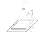
- FIG. 2 is a schematic diagram showing the configuration of the device used in the test.
- FIG. 3 is a diagram showing the result of comparing the relationship between the signal intensity and the wavelength of the pattern-like defective portion and the healthy portion.
- FIG. 4 is a diagram showing the results of comparing the relationship between the incident angle of the illumination light, the signal intensity difference between the pattern-like defect portion and the sound portion, and the wavelength.
- FIG. 5 is a schematic diagram showing the configuration of the surface inspection apparatus for metal materials according to the first embodiment of the present invention.
- FIG. 6 is a schematic diagram showing the configuration of a surface inspection apparatus for metal materials according to a second embodiment of the present invention.
- FIG. 7 is a flow chart showing the flow of surface inspection processing, which is one embodiment of the present invention.
- FIG. 8 is a diagram showing an example of a difference image.
- FIG. 9 is a diagram showing an example of a difference image.
- a thick steel plate which is a type of steel product, is covered with an oxide film called black scale on the surface, and a pattern called harmless pattern, which does not affect the quality of the steel product, may occur.
- pattern defects such as scabs occur on the surface of thick steel plates, but as shown in FIG. 1, it is difficult to distinguish between pattern defects and harmless patterns based on the difference in brightness. Therefore, the inventors of the present invention have focused on the fact that minute red scales (Fe 2 O 3 ) are likely to be generated on the pattern-like defects, and the red scales make the pattern-like defects look reddish.
- a test was conducted to detect pattern defects using the characteristics.
- Fig. 2 shows the configuration of the device used for the test. As shown in FIG.
- a thick steel plate sample SA having pattern defects was placed on a linear stage 1, and illumination light L having a broadband wavelength from a xenon light source 2 was applied to the surface of the thick steel plate sample SA.
- a spectroscopic image of each wavelength was taken using a spectroscopic camera 3 having a one-dimensional field of view.
- Fig. 3 shows the result of comparing the relationship between the signal intensity and the wavelength of the pattern-like defect part and the healthy part using the spectroscopic image.
- the signal intensity characteristics on the short wavelength side and the long wavelength side are relatively different between the pattern-like defect portion and the sound portion. This suggests that pattern-like defects, which were difficult to detect by harmless pattern signals at a single wavelength alone, may be detectable by comparing signal intensities between wavelengths. Therefore, the spectral image of the 415 nm wavelength band (415 nm image) and the spectral image of the 750 nm wavelength band (750 nm image) are subjected to luminance correction so that the average value of luminance is constant.
- FIG. 8 shows an image obtained by taking the difference in luminance value. As shown in FIG. 8, the signal of the harmless pattern is canceled by the difference, and the signal of the pattern-like defect is emphasized.
- FIG. 4 shows the results of comparing the incident angle of the illumination light L (the angle with respect to the surface normal vector of the steel plate), the signal intensity difference between the pattern-like defect portion and the sound portion, and the wavelength. Incident angles are described as 20°, 30°, etc. in the legend of FIG. As shown in FIG. 4, as the incident angle of the illumination light L increases, the signal intensity difference between the short wavelength side and the long wavelength side increases. Therefore, the incident angle of the illumination light L should be increased in order to efficiently detect the spectral reflection characteristics of the object, that is, the color difference.
- the pattern-like defect of a thick steel plate has been described, but the present invention can be applied to the detection of a surface defect having a spectral reflection characteristic different from that of a sound portion occurring on the surface of other metal materials.
- FIG. 5 A surface inspection apparatus for metal materials, which is one embodiment of the present invention, conceived from the above technical idea, will be described below with reference to FIGS. 5 to 8.
- FIG. 5 A surface inspection apparatus for metal materials, which is one embodiment of the present invention, conceived from the above technical idea, will be described below with reference to FIGS. 5 to 8.
- FIG. 5 A surface inspection apparatus for metal materials, which is one embodiment of the present invention, conceived from the above technical idea, will be described below with reference to FIGS. 5 to 8.
- FIG. 5 is a schematic diagram showing the configuration of the surface inspection apparatus for metal materials according to the first embodiment of the present invention.
- a metal material surface inspection apparatus 10 according to a first embodiment of the present invention is an apparatus for detecting surface defects in a plate-shaped steel material S conveyed in the direction of the arrow in the drawing.
- a metal material surface inspection apparatus 10 according to the first embodiment of the present invention includes a light source 11, an encoder and pulse generator 12, an area sensor 13 capable of capturing spectral images in a plurality of wavelength bands, an image processing device 14, and A monitor 15 is provided as a main component.
- the light source 11 irradiates the inspection target portion on the surface of the steel material S with the illumination light L according to the trigger signal output by the pulse generator every time the pulse signal is transmitted from the encoder a certain number of times.
- the light source 11 is preferably arranged so that the irradiation direction of the illumination light L is inclined within a range of 60° or more and less than 90° with respect to the normal line direction of the steel material S surface. As a result, surface defects can be accurately detected from the difference image.
- a plurality of light sources 11 may be arranged.
- a xenon light source is used as the light source 11.
- the light source 11 includes components of a plurality of different wavelength bands
- a light source with broadband characteristics such as a metal halide light source, a halogen light source, a mercury lamp, and an incandescent lamp may be used.
- the light sources may also be a combination of light sources with specific narrowband characteristics such as LEDs or lasers.
- a flash light source or pulse lighting may be used to prevent image blurring.
- the area sensor 13 captures spectral images of a plurality of different wavelength bands at approximately the same position of the steel material S.
- a plurality of captured spectral images are preferably coaxial, but may be aligned by image processing.
- a filter that transmits different wavelength bands is attached to each element so as to be nested, and a Bayer method that generates a plurality of images later or a prism and a plurality of elements are used to adjust so that they are coaxial. Prism type.
- the wavelength band for receiving light may be narrow band with a wavelength selection filter or the like if there is a margin in the amount of light.
- at least one of a plurality of different wavelength bands should include a narrow wavelength band of 650 nm or more, and at least one should include a narrow wavelength band of 500 nm or less.
- the area sensor 13 captures a spectroscopic image in synchronization with the light source 11 according to the trigger signal output from the pulse generator. Except for the spectral image in which the edge of the steel material S is photographed, it is assumed that the luminance value of each channel of the spectral image is not saturated.
- two-channel area sensors that capture light in long and short wavelength bands are used, but the apparatus may be configured to image three or more wavelength bands with three or more channels of area sensors.
- the area sensor 13 preferably receives the reflected light so that the light-receiving angle with respect to the normal direction of the surface of the steel material S is in the range of 0° or more and less than 20°.
- the image processing device 14 detects surface defects in the inspected portion by performing differential processing, which will be described later, between spectral images input from each channel of the area sensor 13 . Then, the image processing device 14 outputs to the monitor 15 the spectral image input from the area sensor 13 , the spectral image after differential processing, and information on the surface defect detection result.
- FIG. 6 is a schematic diagram showing the configuration of a surface inspection apparatus for metal materials according to a second embodiment of the present invention.
- a metal material surface inspection apparatus 20 according to a second embodiment of the present invention detects surface defects in a plate-shaped steel material S conveyed in the direction of the arrow in the figure.
- the difference from the metal material surface inspection apparatus 10 of the first embodiment is that the light source 11 is a line light source 21 and the area sensor 13 is a line sensor 22 .
- the line sensor 22 By using the line sensor 22, the field of view becomes only one line, and compared with the first embodiment, there is an advantage that the optical conditions are stable. Disadvantages such as vulnerability to positional fluctuations also exist.
- the metal material surface inspection apparatuses 10 and 20 having such a configuration perform the following surface inspection processing, thereby distinguishing pattern-like defective portions from healthy portions having harmless patterns in the inspected portion.
- the pattern-like defect described here is a defect that does not appear to have unevenness from the surface, such as a foreign matter being pressed or scale being formed on a concave defect.
- the healthy portion with harmless patterns means a portion having a surface film or surface properties different in optical characteristics from the base iron portion with a thickness of several to several tens of ⁇ m, such as black scale, and is inspected for surface inspection. This is the part that causes noise in processing.
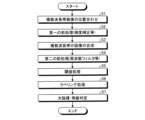
- FIG. 7 is a flow chart showing the flow of surface inspection processing, which is one embodiment of the present invention.
- the surface inspection process shown in FIG. 7 starts at the timing when a command to execute the surface inspection process is input to the image processing device 14, and the surface inspection process proceeds to the process of step S1.
- step S1 the image processing device 14 performs alignment processing when the positions of the spectral images of a plurality of different wavelength bands are shifted pixel by pixel. If spectral images cannot be captured coaxially, it is necessary to align the spectral images of different wavelength bands.
- the alignment method changes depending on the form of the positional deviation of the spectral images of each wavelength band, and it is preferable to perform processing such as translation, linear conversion, and one-to-one correspondence between pixels as necessary. Thereby, the process of step S1 is completed, and the surface inspection process proceeds to the process of step S2.
- step S2 the image processing device 14 performs first preprocessing such as correction to keep the average brightness constant for a plurality of spectral images of different wavelength bands, brightness unevenness correction, signal intensity normalization processing, and the like. to run. Thereby, the process of step S2 is completed, and the surface inspection process proceeds to the process of step S3.
- first preprocessing such as correction to keep the average brightness constant for a plurality of spectral images of different wavelength bands, brightness unevenness correction, signal intensity normalization processing, and the like.
- the image processing device 14 compares a plurality of spectral images in different wavelength bands, and generates a composite processed image that emphasizes only pattern defects by utilizing differences in spectral reflection characteristics. Specifically, the image processing device 14 selects two spectral images having a large difference in spectral reflectance characteristics, and calculates the luminance difference, ratio, etc., between the two spectral images to generate a synthetic processed image. . A case will be described in which a difference image between two spectral images is generated as a synthesized processed image.
- the image processing device 14 calculates the luminance value of the first spectral image Ib (for example, the luminance value of the first channel having sensitivity characteristics corresponding to the wavelength band on the short wavelength side) as shown in the following formula (1). ) by subtracting the luminance value of the second spectral image Ir (for example, the luminance value of the second channel having sensitivity characteristics corresponding to the wavelength band on the long wavelength side) Ir (x, y) from Ib (x, y) A luminance value Id1 (x, y) of the difference image Id1 is calculated.
- the luminance value of the first spectral image Ib for example, the luminance value of the first channel having sensitivity characteristics corresponding to the wavelength band on the short wavelength side
- the spectral images Ib and Ir are images with the number of pixels X ⁇ Y. Further, in the xy coordinate system of two orthogonal axes set for each of the spectral images Ib and Ir, the x coordinate is 1 ⁇ x ⁇ X and the y coordinate is 1 ⁇ y ⁇ Y. Further, in this example, a difference image is generated as a composite processed image, but an image having a ratio of luminance values using Equation (2) shown below may be generated as a composite processed image. Alternatively, the luminance values of the two spectral images may be threshold-processed separately, and then AND-processed to generate a composite processed image.
- step S3 is completed, and the surface inspection process proceeds to the process of step S4.
- (a) Space conversion method This method is effective for three-channel, particularly color images, and is a method for generating an image that extracts the influence of spectral reflection characteristics (color) by converting the color space.
- Color spaces after conversion include an HSV space and an HLS space, and information on spectral reflection characteristics appears in hue information in each of them.
- threshold processing may be performed on the luminance value of each color image after conversion to XYZ, L*u*v*, and L*a*b* spaces and normalizing the luminance component.
- Statistical Multivariate Analysis Method This is a method of extracting portions having different spectral reflectance characteristics by statistical multivariate analysis, using the luminance values of each wavelength band of each pixel as feature amount vectors.
- PCA principal component analysis
- the Mahalanobis distance of each pixel is the representative of that pixel. Reconstruct the image as values. Since the pattern-like defect portion has a different color tone, it is expected that the Mahalanobis distance is larger than that of the healthy portion.
- principal component analysis has been described here, the same effect can be obtained by similarly calculating the degree of divergence from the model using a Gaussian mixture model, independent component analysis, or regression model.
- (c) Machine learning method The method is the same as the statistical multivariate analysis method up to the point where the luminance value of each wavelength band of each pixel is used as a feature vector. is supervised, and a judging machine is created by general supervised learning to judge whether each pixel is a pattern-like defective portion or a normal portion.
- k-means kernel method, decision tree method, Gaussian mixture model, regression model, or the like may be used.
- this method is used, the threshold processing described later is not necessary, and pixels that are defect candidates can be directly extracted.
- step S4 the image processing device 14 generates an image in which surface defects are emphasized by performing second preprocessing using a frequency filter or the like on the composite processed image. Thereby, the process of step S4 is completed, and the surface inspection process proceeds to the process of step S5.
- step S5 the image processing device 14 generates a binarized image by performing threshold processing on the luminance values of the image obtained by the process of step S4. Thereby, the process of step S5 is completed, and the surface inspection process proceeds to the process of step S6.
- step S6 the image processing device 14 performs connected/isolated point removal on the binarized image by processing such as expansion/contraction processing as necessary, and then considers adjacent pixels as blobs. A labeling process is performed to label the Then, the image processing device 14 uses the blob extracted by the labeling process as a surface defect candidate portion. Thereby, the process of step S6 is completed, and the surface inspection process proceeds to the process of step S7.
- the image processing device 14 determines the type and grade of the surface defect (including harmless) for each surface defect candidate portion obtained by the process of step S6.
- Judgment methods can be manually defined judgment rules, regression models (linear regression, logistic regression, multiple regression, support vector machines, nonlinear kernels, etc.), decision tree models, random forests, Bayesian estimation models, mixed Gaussian models, These models may be automatically generated by a general machine learning method using feature quantities such as a boosting method. In this case, by adding each representative value (average/maximum) of the luminance values of multiple spectral images and values (sum/difference/ratio) with which each representative value can be compared to the feature quantity, the spectral reflectance characteristics can be calculated.
- a convolutional neural network may also be used if enough N numbers of data are obtained. Also, a plurality of machine learning techniques may be combined. The determination result is displayed on the monitor 15 and used for guidance, or is collected by the server and used for determining whether the steel material S can be shipped and whether maintenance is necessary. As a result, the processing of step S7 is completed, and a series of surface inspection processing ends.
- the surface of the steel material S is irradiated with light, and two reflected light beams from the surface of the steel material S due to the irradiated light are obtained. Images are taken in different wavelength bands as described above, and surface defects present on the surface of the steel material S are detected from information on relative signal intensities between a plurality of images obtained from the same position on the surface of the steel material S. As a result, the surface defects of the steel material S can be accurately detected without omission.
- the presence or absence of surface defects in a metal material such as steel S is investigated using the surface inspection process, which is one embodiment of the present invention, and the occurrence of surface defects (incidence rate, defect size, etc.) is determined to a predetermined allowable level. Carry out quality assurance to confirm whether the product is substandard. This makes it possible to provide a metal material with guaranteed surface properties. In practice, quality can be guaranteed by stating, for example, whether or not surface defects are below a predetermined allowable standard in a statement of delivery or an inspection certificate.
- Example 1 As Example 1, an example of detecting surface defects in a thick steel plate using the present invention will be shown.
- the surface defects are in the form of pressure bonding to the steel plate surface during the manufacturing process of the steel plate, and when viewed from the steel plate surface, there are no uneven portions.
- FIG. 8 shows a difference image obtained by taking a spectral image in a wavelength band of 415 nm and a spectral image in a wavelength band of 750 nm for a surface defect of a steel plate, performing brightness correction so that the average value is constant, and taking the difference. Signals of harmless patterns such as black scales are canceled by the difference, and only signals of pattern-like defects are emphasized.
- the characteristics of the spectral reflectance spectra of the surface defective portion and the normal portion are utilized to generate a spectral image obtained by capturing the light on the long wavelength side and the spectral image on the short wavelength side. It was confirmed that defects can be detected with high accuracy.
- surface layer scale having a surface reflection spectrum similar to that of the surface defect portion may be generated in the sound portion. By discriminating the surface defects, it is possible to suppress over-detection and detect surface defects with high accuracy.
- Example 2 As Example 2, an example in which the present invention is used to detect the red scale of a steel plate is shown. On the surface of the thick steel plate, red scales, black scales, and base iron portions where the scales are peeled off are unevenly present.
- the scale of hot-manufactured steel materials becomes layered as oxidation progresses , and is composed of wustite (FeO), magnetite ( Fe3O4 ), and hematite ( Fe2O3 ) in the order closest to the base iron . There are many.
- the scale on the surface is mainly composed of wustite or magnetite, it becomes a black scale, and tends to be a uniform scale that has high mechanical strength and is difficult to peel off.
- red scale tends to be avoided because it easily peels off and adheres to factory equipment and stains it, as well as causing unevenness in the color tone of the final product.
- brightness correction was performed so that the average value of the brightness of the R component and B component images was constant, and the difference between the R component image and the B component image was calculated. The images taken are shown in FIGS. 9(a) and 9(b).
- the camera elements and filters were designed so that the R channel could capture images in a narrow wavelength band of 650 nm or more, and the B channel could capture images in a narrow wavelength band of 500 nm or less.
- the signals of the black scale and the base iron portion are canceled by the difference, and only the signal of the red scale is emphasized.
- a two-dimensional image obtained by capturing light on the long wavelength side and a two-dimensional image captured by capturing light on the short wavelength side by utilizing the characteristics of the spectral reflection spectra of the red scale and the black scale. It was confirmed that the red scale can be detected with high accuracy by creating a differential image.
- quality assurance is performed by calculating the ratio and degree of the red scale generation area to the entire surface of the steel plate, and the distribution of red scale generation is used for temperature control in the rolling process and for detecting abnormalities in descaling equipment. can be
- the present invention it is possible to provide a surface inspection method and a surface inspection apparatus for metal materials that can accurately detect surface defects in metal materials without omission. Moreover, according to the present invention, it is possible to provide a high-quality metal material free from surface defects.
Landscapes
- Engineering & Computer Science (AREA)
- Textile Engineering (AREA)
- Physics & Mathematics (AREA)
- Health & Medical Sciences (AREA)
- Life Sciences & Earth Sciences (AREA)
- Chemical & Material Sciences (AREA)
- Analytical Chemistry (AREA)
- Biochemistry (AREA)
- General Health & Medical Sciences (AREA)
- General Physics & Mathematics (AREA)
- Immunology (AREA)
- Pathology (AREA)
- Investigating Materials By The Use Of Optical Means Adapted For Particular Applications (AREA)
Abstract
本発明に係る金属材料の表面検査方法は、金属材料の表面欠陥を光学的に検出する金属材料の表面検査方法であって、金属材料の表面に対して光を照射する照射ステップと、照射ステップにおいて照射された光による金属材料の表面からの反射光を2つ以上の異なる波長帯で撮像することによって複数の画像を得る撮像ステップと、撮像ステップにおいて金属材料の表面の同位置から得られた複数の画像間の相対信号強度の情報から金属材料の表面に存在する表面欠陥を検出する検出ステップと、を含む。
Description
本発明は、金属材料の表面欠陥を光学的に検出する金属材料の表面検査方法、金属材料の表面検査装置、及び金属材料に関する。
近年、金属材料、特に鉄鋼製品の製造工程では、大量不適合防止による歩留まり向上の観点から、熱間又は冷間で鋼材の表面欠陥を検出することが求められている。ここで述べる鋼材とは、継目無鋼管、溶接鋼管、熱延鋼板、冷延鋼板、厚板等の鋼板や形鋼をはじめとする鉄鋼製品及びこれらの鉄鋼製品が製造される過程で生成されるスラブ等の半製品のことを意味する。このため、鋼材の表面欠陥を検出する方法として、継目無鋼管の製造工程におけるビレットに光を照射して反射光を受光し、反射光の光量によって表面欠陥の有無を判別する方法が提案されている(特許文献1参照)。また、熱間鋼材から放射される自発光と相互に影響を及ぼさず、互いに影響を及ぼし合うことのない複数の波長域の可視光を、熱間鋼材表面の法線に対し互いに対称な斜め方向から照射し、合成反射光による像及び個々の反射光による像を熱間鋼材表面の法線方向で得て、これらの像の組み合わせから熱間鋼材の表面欠陥を検出する方法も提案されている(特許文献2参照)。また、鋼材表面の法線に対し互いに対称な傾斜方向から弁別可能な照明光を照射し、各方向から照明された検査対象部位をそれぞれ撮像した2つの画像の差分画像から、凹形状に対応する明部及び暗部の配列を抽出し、鋼材の表面欠陥を検出する方法も提案されている(特許文献3参照)。
特許文献1に記載の方法によれば、スケールや無害模様の反射率が地鉄部分の反射率とは異なることから、表面欠陥ではない健全部に発生したスケールや無害模様を表面欠陥と誤検出してしまう可能性がある。このため、特許文献1に記載の方法では、ビレットの表面欠陥(表面疵)の形状が直線的であることを利用して、表面欠陥とスケールとを弁別している。しかしながら、鋼材の表面欠陥には、直線状のものに限らず、円形状等の様々な形状のものがある。このため、特許文献1に記載の方法を鋼材の表面欠陥の検出処理に適用することは難しい。一方、特許文献2に記載の方法では、表面欠陥、スケール、無害模様等の種類が膨大にあることから、単純に像を組み合わせるだけではスケールや無害模様と表面欠陥とを弁別することは困難である。また、膨大な像の組み合わせに対応した検出ロジックを構築することは現実的には困難である。また、特許文献3に記載の方法によれば、上記課題を解決して鋼材表面の凹状欠陥を精度よく検出できる。ところが、鋼材の表面欠陥は凹状のものに限らず、異物が圧着した状態で圧延加工を実施した場合や凹状欠陥部にスケールが生成した場合に、表面からの見かけ上凹凸が見られない欠陥も存在する。このため、特許文献3に記載の方法のみでは、鋼材に発生する表面欠陥を洩れなく検出することは困難である。
本発明は、上記課題に鑑みてなされたものであって、その目的は、金属材料の表面欠陥を洩れなく精度よく検出可能な金属材料の表面検査方法及び表面検査装置を提供することにある。また、本発明の他の目的は、表面欠陥のない高品質な金属材料を提供することにある。
本発明に係る金属材料の表面検査方法は、金属材料の表面欠陥を光学的に検出する金属材料の表面検査方法であって、前記金属材料の表面に対して光を照射する照射ステップと、前記照射ステップにおいて照射された光による前記金属材料の表面からの反射光を2つ以上の異なる波長帯で撮像することによって複数の画像を得る撮像ステップと、前記撮像ステップにおいて前記金属材料の表面の同位置から得られた複数の画像間の相対信号強度の情報から前記金属材料の表面に存在する表面欠陥を検出する検出ステップと、を含む。
前記検出ステップは、前記複数の画像間の相対強度又は該相対強度から計算される複数の量を特徴量として機械学習手法によって作成された判定器を用いて前記表面欠陥を検出するステップを含むとよい。
前記照射ステップは、前記金属材料の表面の法線方向に対する角度が60°以上90°未満の範囲内になるように前記光を照射するステップを含み、前記撮像ステップは、前記金属材料の表面に対する受光角度が0°以上20°未満の範囲内になるように前記反射光を受光するステップを含むとよい。
前記2つ以上の異なる波長帯の少なくとも1つは500nm以下の波長帯であるとよい。
前記2つ以上の異なる波長帯の少なくとも1つは650nm以上の波長帯であるとよい。
本発明に係る金属材料の表面検査装置は、金属材料の表面欠陥を光学的に検出する金属材料の表面検査装置であって、前記金属材料の表面に対して光を照射する照射手段と、前記照射手段によって照射された光による前記金属材料の表面からの反射光を2つ以上の異なる波長帯で撮像することによって複数の画像を得る撮像手段と、前記撮像手段によって前記金属材料の表面の同位置から得られた複数の画像間の相対信号強度の情報から、前記金属材料の表面に存在する表面欠陥を検出する検出手段と、を備える。
本発明に係る金属材料は、本発明に係る金属材料の表面検査方法を用いて表面性状が保証されている。
本発明に係る金属材料の表面検査方法及び表面検査装置によれば、金属材料の表面欠陥を洩れなく精度よく検出することができる。また、本発明に係る金属材料によれば、表面欠陥のない高品質な金属材料を提供することができる。
鉄鋼製品の一種である厚鋼板では、表面が黒皮スケールと呼ばれる酸化膜に覆われ、無害模様と称される、鉄鋼製品の品質には影響を及ぼさない模様が発生することがある。また、厚鋼板では、ヘゲ等の模様状欠陥も表面に発生するが、図1に示ように輝度の差では模様状欠陥と無害模様とを区別することは難しい。そこで、本発明の発明者らは、模様状欠陥上には微小な赤スケール(Fe2O3)が生成しやすく、この赤スケールによって模様状欠陥は赤み掛かって見えることに着目し、分光反射特性を利用して模様状欠陥を検出する試験を行った。試験に使用した装置の構成を図2に示す。図2に示すように、本試験では、模様状欠陥を有する厚鋼板サンプルSAをリニアステージ1の上に載置し、キセノン光源2から広帯域の波長を有する照明光Lを厚鋼板サンプルSAの表面に照射し、1次元の視野を有する分光カメラ3を用いて各波長の分光画像を撮影した。
図3に分光画像を用いて模様状欠陥部及び健全部の信号強度と波長の関係を比較した結果を示す。図3に示すように、模様状欠陥部と健全部とでは、短波長側及び長波長側における信号強度の特性が相対的に異なっている。これは、単一の波長だけでは無害模様の信号によって検出が困難であった模様状欠陥が波長間の信号強度の比較によって検出できる可能性があることを示唆する。そこで、415nmの波長帯の分光画像(415nm画像)と750nmの波長帯の分光画像(750nm画像)に対して輝度の平均値が一定となるよう輝度補正を実施した後、2枚の分光画像の輝度値の差分を取った画像を図8に示す。図8に示すように、無害模様の信号が差分によってキャンセルされ、模様状欠陥の信号が強調されている。
以上のことから、異なる複数の波長間の輝度情報を比較することによって健全部と分光反射特性が異なる模様状欠陥を精度よく検出できることが確認された。また、図4に照明光Lの入射角(厚鋼板の表面法線ベクトルに対する角度)と、模様状欠陥部と健全部の信号強度差と波長の関係を比較した結果を示す。図4の凡例で20°,30°等と記載されたものが入射角である。図4に示すように、照明光Lの入射角が大きくなるほど、短波長側と長波長側の信号強度差が大きくなっている。従って、対象の分光反射特性、すなわち色味の差を効率的に検出するためには、照明光Lの入射角を大きくするとよい。上記の説明では厚鋼板の模様状欠陥について述べたが、本発明は他の金属材料の表面に発生する健全部と分光反射特性が異なる表面欠陥の検出に適用することができる。
以下、図5~図8を参照して、上述した技術思想から想到された、本発明の一実施形態である金属材料の表面検査装置について説明する。
図5は、本発明の第1の実施形態である金属材料の表面検査装置の構成を示す模式図である。図5に示すように、本発明の第1の実施形態である金属材料の表面検査装置10は、図示矢印方向に搬送される板形状の鋼材Sの表面欠陥を検出する装置である。本発明の第1の実施形態である金属材料の表面検査装置10は、光源11、エンコーダ及びパルス生成器12、複数の波長帯の分光画像を撮影可能なエリアセンサ13、画像処理装置14、及びモニター15を主な構成要素として備えている。
光源11は、エンコーダから一定回数パルス信号が送信される度にパルス生成器が出力するトリガー信号に従って鋼材Sの表面上の検査対象部位に照明光Lを照射する。光源11は、鋼材S表面の法線方向に対して照明光Lの照射方向が60°以上90°未満の範囲内で傾くように配置するとよい。これにより、差分画像から表面欠陥を精度よく検出できる。また、本実施形態では光源11を1個配置しているが、光源11を複数配置してもよい。また、本実施形態では、光源11としてキセノン光源を採用したが、異なる複数の波長帯の成分が含まれているのであれば、メタハラ光源やハロゲン光源、水銀灯、白熱灯等の広帯域の特性を持つ光源でも、LEDやレーザー等の特定の狭帯域の特性を持つ光源を組み合わせてもよい。また、鋼材Sの搬送速度が速い、決められた搬送位置(パスライン)からの鋼材Sの位置変動が大きい等といった場合には、撮像ブレを防ぐためにフラッシュ光源やパルス点灯を用いてもよい。
エリアセンサ13は、鋼材Sの概同一位置の異なる複数の波長帯の分光画像を撮影する。撮影される複数の分光画像は同軸であるとよいが、画像処理によって位置合わせをしてもよい。また、エリアセンサ13としては、各素子に入れ子となるよう異なる波長帯を透過するフィルターを張り付け、後から複数の画像を生成するベイヤー式やプリズムと複数の素子を用いて同軸となるよう調整するプリズム式が挙げられる。また、RGBのカラーカメラを用いることが安価で好ましいが、2チャンネルや4チャンネル以上のマルチバンドエリアセンサを用いてもよい。さらに、弁別したい健全部と表面欠陥部の分光反射特性により、エリアセンサ13や光源11の前面等の光路上に波長選択フィルターを設置することにより、より色味を際立たせることで検出能を向上させてもよい。また、健全部と表面欠陥部の分光反射特性の差が狭帯域で現れる場合、光量に余裕があれば波長選択フィルター等で受光する波長帯を狭帯域としてもよい。また、模様状欠陥を検出する場合には、異なる複数の波長帯のうち少なくとも一つが650nm以上の狭域の波長帯を含み、少なくとも一つが500nm以下の狭域の波長帯を含むとよい。
エリアセンサ13は、パルス生成器から出力されるトリガー信号に従って光源11と同期して分光画像を撮影する。鋼材Sの端部が撮影されている分光画像を除き、分光画像の各チャンネルの輝度値はサチュレーションしていないものとする。また、本実施形態では長波長帯及び短波長帯の光を捉える2チャンネルのエリアセンサを用いたが、別途3以上の波長帯を3チャンネル以上のエリアセンサで撮像する装置構成としてもよい。また、エリアセンサ13は、鋼材Sの表面の法線方向に対する受光角度が0°以上20°未満の範囲内になるように反射光を受光するとよい。
画像処理装置14は、エリアセンサ13の各チャンネルから入力された分光画像間で後述する差分処理を行うことによって検査対象部位における表面欠陥を検出する。そして、画像処理装置14は、エリアセンサ13から入力された分光画像、差分処理後の分光画像及び、表面欠陥の検出結果に関する情報をモニター15に出力する。
〔第2の実施形態〕
図6は、本発明の第2の実施形態である金属材料の表面検査装置の構成を示す模式図である。図6に示すように、本発明の第2の実施形態である金属材料の表面検査装置20は、図示矢印方向に搬送される板形状の鋼材Sの表面欠陥を検出する。第1の実施形態である金属材料の表面検査装置10との違いは、光源11をライン光源21とし、エリアセンサ13をラインセンサ22としている点である。ラインセンサ22を用いることで視野が1ライン上のみとなり、第1の実施形態と比較して、光学条件が安定するといったメリットがある一方、搬送中の搬送位置(パスライン)からの鋼材Sの位置変動に弱い等のデメリットも存在する。
図6は、本発明の第2の実施形態である金属材料の表面検査装置の構成を示す模式図である。図6に示すように、本発明の第2の実施形態である金属材料の表面検査装置20は、図示矢印方向に搬送される板形状の鋼材Sの表面欠陥を検出する。第1の実施形態である金属材料の表面検査装置10との違いは、光源11をライン光源21とし、エリアセンサ13をラインセンサ22としている点である。ラインセンサ22を用いることで視野が1ライン上のみとなり、第1の実施形態と比較して、光学条件が安定するといったメリットがある一方、搬送中の搬送位置(パスライン)からの鋼材Sの位置変動に弱い等のデメリットも存在する。
このような構成を有する金属材料の表面検査装置10,20は、以下に示す表面検査処理を実行することによって、検査対象部位における模様状欠陥部と無害模様を持つ健全部とを弁別する。ここで述べる模様状欠陥とは、異物が圧着したり、凹状欠陥上にスケールが生成したりする等して、表面からの見かけ上凹凸が存在しない欠陥とする。また、無害模様を持つ健全部とは、黒皮スケール等の厚さ数~数十μm程度の地鉄部分とは光学特性の異なる表面被膜や表面性状を有する部分のことを意味し、表面検査処理においてノイズ要因となる部分である。
〔表面検査処理〕
図7は、本発明の一実施形態である表面検査処理の流れを示すフローチャートである。図7に示す表面検査処理は、画像処理装置14に対して表面検査処理の実行指令が入力されたタイミングで開始となり、表面検査処理はステップS1の処理に進む。
図7は、本発明の一実施形態である表面検査処理の流れを示すフローチャートである。図7に示す表面検査処理は、画像処理装置14に対して表面検査処理の実行指令が入力されたタイミングで開始となり、表面検査処理はステップS1の処理に進む。
ステップS1の処理では、画像処理装置14が、異なる複数の波長帯の分光画像の位置が画素単位でずれている場合、位置合わせ処理を実施する。分光画像を同軸で撮像できない場合、異なる複数の波長帯の分光画像間で位置合わせが必要となる。位置合わせ方法は、各波長帯の分光画像の位置ずれの形態によって変化し、必要に応じて平行移動や線形変換、画素を1対1対応させる等の処理を実行するとよい。これにより、ステップS1の処理は完了し、表面検査処理はステップS2の処理に進む。
ステップS2の処理では、画像処理装置14が、異なる波長帯の複数の分光画像に対して輝度の平均値を一定とする補正や輝度むら補正、信号強度の正規化処理等の第一の前処理を実行する。これにより、ステップS2の処理は完了し、表面検査処理はステップS3の処理に進む。
ステップS3の処理では、画像処理装置14が、異なる波長帯の複数の分光画像を比較し、分光反射特性の違いを活用して模様状欠陥のみを強調した合成処理画像を生成する。具体的には、画像処理装置14は、分光反射特性の違いが大きい2枚の分光画像を選定し、2枚の分光画像の輝度の差や比等を算出することにより合成処理画像を生成する。2枚の分光画像の差分画像を合成処理画像として生成する場合について説明する。この場合、画像処理装置14は、以下の数式(1)に示すように、第1の分光画像Ibの輝度値(例えば短波長側の波長帯に対応する感度特性を有する第1チャンネルの輝度値)Ib(x,y)から第2の分光画像Irの輝度値(例えば長波長側の波長帯に対応する感度特性を有する第2チャンネルの輝度値)Ir(x,y)を減算することにより差分画像Id1の輝度値Id1(x,y)を算出する。

分光画像Ib,Irは画素数X×Yの画像とする。また、分光画像Ib,Irのそれぞれに設定した直行2軸のxy座標系においてx座標は1≦x≦Xとし、y座標は1≦y≦Yとする。また、本例では、合成処理画像として差分画像を生成したが、以下に示す数式(2)を用いた輝度値の比の画像を合成処理画像として生成してもよい。また、2枚の分光画像の輝度値に対して別々に閾値処理を実行した後にAND処理を実施して合成処理画像を生成してもよい。

また、本処理は2枚の分光画像だけで実行可能であるが、特に3枚以上の分光画像に有効な手段として以下に示す手法(a)~(c)が挙げられる。これにより、ステップS3の処理は完了し、表面検査処理はステップS4の処理に進む。
(a)空間変換法
3チャンネル、特にカラー画像に有効な手法であり、分光反射特性(色味)の影響を抽出する画像を色空間の変換により生成する手法である。変換後の色空間にはHSV空間やHLS空間があり、それぞれhue(色相)情報に分光反射特性の情報が現れる。その他、XYZ、L*u*v*、L*a*b*空間に変換し、輝度成分を正規化した後に各色の画像の輝度値に対して閾値処理を施してもよい。
3チャンネル、特にカラー画像に有効な手法であり、分光反射特性(色味)の影響を抽出する画像を色空間の変換により生成する手法である。変換後の色空間にはHSV空間やHLS空間があり、それぞれhue(色相)情報に分光反射特性の情報が現れる。その他、XYZ、L*u*v*、L*a*b*空間に変換し、輝度成分を正規化した後に各色の画像の輝度値に対して閾値処理を施してもよい。
(b)統計的多変量解析法
各画素の各波長帯の輝度値を特徴量ベクトルとし、統計的多変量解析により分光反射特性が異なる部分を抽出する手法である。一例として、対象の検査領域を十分大きく分割し、各領域において全画素の各波長帯の輝度値を特徴量ベクトルとして主成分分析(PCA)を実施し、各画素のマハラノビス距離をその画素の代表値として画像を再構築する。模様状欠陥部は色味が異なるため、マハラノビス距離が健全部と比較して大きいことが期待される。ここでは主成分分析について説明したが、混合ガウシアンモデルや独立成分分析や回帰モデルを用いてモデルからの乖離度を同様に算出しても同様の効果が得られる。
各画素の各波長帯の輝度値を特徴量ベクトルとし、統計的多変量解析により分光反射特性が異なる部分を抽出する手法である。一例として、対象の検査領域を十分大きく分割し、各領域において全画素の各波長帯の輝度値を特徴量ベクトルとして主成分分析(PCA)を実施し、各画素のマハラノビス距離をその画素の代表値として画像を再構築する。模様状欠陥部は色味が異なるため、マハラノビス距離が健全部と比較して大きいことが期待される。ここでは主成分分析について説明したが、混合ガウシアンモデルや独立成分分析や回帰モデルを用いてモデルからの乖離度を同様に算出しても同様の効果が得られる。
(c)機械学習法
各画素の各波長帯の輝度値を特徴量ベクトルとするところまでは統計的多変量解析法と同一であるが、予め各特徴量ベクトルに対し模様状欠陥部か健全部を教師付けし、一般的な教師有り学習により判定機を作成して画素毎に模様状欠陥部か健全部かを判定する手法である。特徴量をクラスタリングする手法として、k-meansやカーネル法、決定木法、混合ガウシアンモデル、回帰モデル等を用いてもよい。本手法を用いる場合、後述する閾値処理は不要であり、直接欠陥候補となる画素を抽出することができる。
各画素の各波長帯の輝度値を特徴量ベクトルとするところまでは統計的多変量解析法と同一であるが、予め各特徴量ベクトルに対し模様状欠陥部か健全部を教師付けし、一般的な教師有り学習により判定機を作成して画素毎に模様状欠陥部か健全部かを判定する手法である。特徴量をクラスタリングする手法として、k-meansやカーネル法、決定木法、混合ガウシアンモデル、回帰モデル等を用いてもよい。本手法を用いる場合、後述する閾値処理は不要であり、直接欠陥候補となる画素を抽出することができる。
ステップS4の処理では、画像処理装置14が、合成処理画像に対して周波数フィルター等を用いた第二の前処理を実行することにより表面欠陥部を強調した画像を生成する。これにより、ステップS4の処理は完了し、表面検査処理はステップS5の処理に進む。
ステップS5の処理では、画像処理装置14が、ステップS4の処理により得られた画像の輝度値に対して閾値処理を実行することにより二値化画像を生成する。これにより、ステップS5の処理は完了し、表面検査処理はステップS6の処理に進む。
ステップS6の処理では、画像処理装置14が、二値化画像に対して必要に応じて膨張収縮処理等の処理により連結・孤立点除去を実施した後、隣接したピクセルをブロブ(塊)とみなしてラベル付けするラベリング処理を実施する。そして、画像処理装置14は、ラベリング処理で抽出されたブロブを表面欠陥候補部とする。これにより、ステップS6の処理は完了し、表面検査処理はステップS7の処理に進む。
ステップS7の処理では、画像処理装置14が、ステップS6の処理により得られた各表面欠陥候補部について表面欠陥の種類や等級(無害を含む)を判定する。判定手法は手動で判定ルールを定めてもよいし、回帰モデル(線形回帰、ロジスティック回帰、重回帰、サポートベクターマシン、非線形カーネル等)、決定木モデル、ランダムフォレスト、ベイズ推定モデル、混合ガウシアンモデル、これらのモデルをブースティングした手法等の特徴量を用いた一般的な機械学習方法で自動生成してもよい。この場合、特徴量に複数の分光画像の輝度値の各代表値(平均値・最大)及び各代表値同士が比較可能な値(和・差・比)等を加えることにより、分光反射特性を加味した判定が可能となる。また、データのN数が十分得られれば、畳み込みニューラルネットワークを用いてもよい。また、複数の機械学習手法を組み合わせてもよい。判定結果は、モニター15に表示され、ガイダンスに用いたり、サーバに収集され、鋼材Sの出荷可否・手入れ要否の判断等に用いられたりする。これにより、ステップS7の処理は完了し、一連の表面検査処理は終了する。
以上の説明から明らかなように、本発明の一実施形態である表面検査処理では、鋼材Sの表面に対して光を照射し、照射された光による鋼材Sの表面からの反射光を2つ以上の異なる波長帯で撮像し、鋼材Sの表面の同位置から得られた複数の画像間の相対信号強度の情報から鋼材Sの表面に存在する表面欠陥を検出する。これにより、鋼材Sの表面欠陥を洩れなく精度よく検出することができる。また、本発明の一実施形態である表面検査処理を用いて鋼材S等の金属材料の表面欠陥の有無を調査し、表面欠陥発生状況(発生率やの欠陥の大きさ等)が所定の許容基準以下であるかどうかを確認する品質保証を実施する。これにより、表面性状を保証された金属材料を提供することができる。実務的には、例えば、納品書や検査証明書等で表面欠陥発生状況が所定の許容基準以下であるかどうかを記載することによって品質を保証することができる。
〔実施例1〕
実施例1として、本発明を用いて厚鋼板の表面欠陥を検出した例を示す。表面欠陥は、厚鋼板の製造過程において鋼板表面に圧着した形態となっており、鋼板表面から見た際に凹凸部は存在しない。厚鋼板の表面欠陥において、415nmの波長帯の分光画像と750nmの波長帯の分光画像を撮像し、平均値が一定となるよう輝度補正を実施し、差分を取った画像を図8に示す。黒皮スケール等の無害模様の信号が差分によりキャンセルされ、模様状欠陥の信号のみ強調されている。これにより、表面欠陥部と健全部の分光反射スペクトルの特徴を活かして、長波長側の光を撮像した分光画像と短波長側の光を撮像した分光画像の差分画像を生成することにより、表面欠陥を精度良く検出できることが確認された。厚鋼板の製造条件によっては、健全部に表面欠陥部と類似の表面反射スペクトルを有する表層スケールが生成する場合があるが、機械学習手法によって作成された判定器を用いて、差分画像から抽出された表面欠陥部を弁別することで、過検出を抑制して精度良く表面欠陥を検出することができる。
実施例1として、本発明を用いて厚鋼板の表面欠陥を検出した例を示す。表面欠陥は、厚鋼板の製造過程において鋼板表面に圧着した形態となっており、鋼板表面から見た際に凹凸部は存在しない。厚鋼板の表面欠陥において、415nmの波長帯の分光画像と750nmの波長帯の分光画像を撮像し、平均値が一定となるよう輝度補正を実施し、差分を取った画像を図8に示す。黒皮スケール等の無害模様の信号が差分によりキャンセルされ、模様状欠陥の信号のみ強調されている。これにより、表面欠陥部と健全部の分光反射スペクトルの特徴を活かして、長波長側の光を撮像した分光画像と短波長側の光を撮像した分光画像の差分画像を生成することにより、表面欠陥を精度良く検出できることが確認された。厚鋼板の製造条件によっては、健全部に表面欠陥部と類似の表面反射スペクトルを有する表層スケールが生成する場合があるが、機械学習手法によって作成された判定器を用いて、差分画像から抽出された表面欠陥部を弁別することで、過検出を抑制して精度良く表面欠陥を検出することができる。
〔実施例2〕
実施例2として、本発明を用いて厚鋼板の赤スケールを検出した例を示す。厚鋼板の表面には、赤スケール、黒スケール、及びスケールが剥がれた地鉄部分がムラ状に存在している。熱間で製造された鋼材のスケールは、酸化が進むにつれて層状になり、地鉄に近い順にウスタイト(FeO)、マグネタイト(Fe3O4)、及びヘマタイト(Fe2O3)から構成されることが多い。表面のスケールがウスタイトやマグネタイトを中心に構成される場合、黒スケールとなり、機械的な強度も高く剥がれづらい均一なスケールとなりやすい。一方で、表面のスケールがヘマタイトを中心に構成される場合には、赤スケールとなり、機械的強度が低く剥がれやすい不均一なスケールとなりやすい。赤スケールは、加工性に問題を生じさせるほか、剥がれやすい性質から工場内の設備に付着して汚れたり、最終製品の色調にムラを生じさせたりすることから忌避される傾向にあり、表面欠陥の一種として扱う場合がある。RGBのカラーカメラで撮像した厚鋼板の表面画像について、R成分及びB成分の画像の輝度の平均値が一定となるように輝度補正を実施し、R成分の画像とB成分の画像で差分を取った画像を図9(a),(b)に示す。Rチャンネルは650nm以上の狭域の波長帯、Bチャンネルは500nm以下の狭域の波長帯で撮像を行えるように、カメラ素子及びフィルターを設計した。図9(a),(b)に示すように、黒スケールや地鉄部分の信号が差分によってキャンセルされ、赤スケールの信号のみが強調されていることがわかる。以上のことから、本発明によれば、赤スケールと黒スケールの分光反射スペクトルの特徴を活かして、長波長側の光を撮像した2次元画像と短波長側の光を撮像した2次元画像の差分画像を作成することにより、赤スケールを精度良く検出することができることが確認できた。実際の運用においては、厚鋼板全面に対する赤スケール発生領域の割合や程度を算出することで品質保証を行ったり、赤スケールの発生分布を圧延工程での温度制御やデスケーリング設備の異常検知に用いたりすることができる。
実施例2として、本発明を用いて厚鋼板の赤スケールを検出した例を示す。厚鋼板の表面には、赤スケール、黒スケール、及びスケールが剥がれた地鉄部分がムラ状に存在している。熱間で製造された鋼材のスケールは、酸化が進むにつれて層状になり、地鉄に近い順にウスタイト(FeO)、マグネタイト(Fe3O4)、及びヘマタイト(Fe2O3)から構成されることが多い。表面のスケールがウスタイトやマグネタイトを中心に構成される場合、黒スケールとなり、機械的な強度も高く剥がれづらい均一なスケールとなりやすい。一方で、表面のスケールがヘマタイトを中心に構成される場合には、赤スケールとなり、機械的強度が低く剥がれやすい不均一なスケールとなりやすい。赤スケールは、加工性に問題を生じさせるほか、剥がれやすい性質から工場内の設備に付着して汚れたり、最終製品の色調にムラを生じさせたりすることから忌避される傾向にあり、表面欠陥の一種として扱う場合がある。RGBのカラーカメラで撮像した厚鋼板の表面画像について、R成分及びB成分の画像の輝度の平均値が一定となるように輝度補正を実施し、R成分の画像とB成分の画像で差分を取った画像を図9(a),(b)に示す。Rチャンネルは650nm以上の狭域の波長帯、Bチャンネルは500nm以下の狭域の波長帯で撮像を行えるように、カメラ素子及びフィルターを設計した。図9(a),(b)に示すように、黒スケールや地鉄部分の信号が差分によってキャンセルされ、赤スケールの信号のみが強調されていることがわかる。以上のことから、本発明によれば、赤スケールと黒スケールの分光反射スペクトルの特徴を活かして、長波長側の光を撮像した2次元画像と短波長側の光を撮像した2次元画像の差分画像を作成することにより、赤スケールを精度良く検出することができることが確認できた。実際の運用においては、厚鋼板全面に対する赤スケール発生領域の割合や程度を算出することで品質保証を行ったり、赤スケールの発生分布を圧延工程での温度制御やデスケーリング設備の異常検知に用いたりすることができる。
以上、本発明者らによってなされた発明を適用した実施の形態について説明したが、本実施形態による本発明の開示の一部をなす記述及び図面により本発明が限定されることはない。すなわち、本実施形態に基づいて当業者等によりなされる他の実施の形態、実施例、及び運用技術等は全て本発明の範疇に含まれる。
本発明によれば、金属材料の表面欠陥を洩れなく精度よく検出可能な金属材料の表面検査方法及び表面検査装置を提供することができる。また、本発明によれば、表面欠陥のない高品質な金属材料を提供することができる。
1 リニアステージ
2 キセノン光源
3 分光カメラ
10,20 金属材料の表面検査装置
11 光源
12 エンコーダ、パルス生成器
13 エリアセンサ
14 画像処理装置
15 モニター
21 ライン光源
22 ラインセンサ
L 照明光
S 鋼材
SA 厚鋼板サンプル
2 キセノン光源
3 分光カメラ
10,20 金属材料の表面検査装置
11 光源
12 エンコーダ、パルス生成器
13 エリアセンサ
14 画像処理装置
15 モニター
21 ライン光源
22 ラインセンサ
L 照明光
S 鋼材
SA 厚鋼板サンプル
Claims (7)
- 金属材料の表面欠陥を光学的に検出する金属材料の表面検査方法であって、
前記金属材料の表面に対して光を照射する照射ステップと、
前記照射ステップにおいて照射された光による前記金属材料の表面からの反射光を2つ以上の異なる波長帯で撮像することによって複数の画像を得る撮像ステップと、
前記撮像ステップにおいて前記金属材料の表面の同位置から得られた複数の画像間の相対信号強度の情報から前記金属材料の表面に存在する表面欠陥を検出する検出ステップと、
を含む、金属材料の表面検査方法。 - 前記検出ステップは、前記複数の画像間の相対強度又は該相対強度から計算される複数の量を特徴量として機械学習手法によって作成された判定器を用いて前記表面欠陥を検出するステップを含む、請求項1に記載の金属材料の表面検査方法。
- 前記照射ステップは、前記金属材料の表面の法線方向に対する角度が60°以上90°未満の範囲内になるように前記光を照射するステップを含み、前記撮像ステップは、前記金属材料の表面に対する受光角度が0°以上20°未満の範囲内になるように前記反射光を受光するステップを含む、請求項1又は2に記載の金属材料の表面検査方法。
- 前記2つ以上の異なる波長帯の少なくとも1つは500nm以下の波長帯である、請求項1~3のうち、いずれか1項に記載の金属材料の表面検査方法。
- 前記2つ以上の異なる波長帯の少なくとも1つは650nm以上の波長帯である、請求項1~3のうち、いずれか1項に記載の金属材料の表面検査方法。
- 金属材料の表面欠陥を光学的に検出する金属材料の表面検査装置であって、
前記金属材料の表面に対して光を照射する照射手段と、
前記照射手段によって照射された光による前記金属材料の表面からの反射光を2つ以上の異なる波長帯で撮像することによって複数の画像を得る撮像手段と、
前記撮像手段によって前記金属材料の表面の同位置から得られた複数の画像間の相対信号強度の情報から、前記金属材料の表面に存在する表面欠陥を検出する検出手段と、
を備える、金属材料の表面検査装置。 - 請求項1~5のうち、いずれか1項に記載の金属材料の表面検査方法を用いて表面性状が保証されている、金属材料。
Priority Applications (1)
| Application Number | Priority Date | Filing Date | Title |
|---|---|---|---|
| JP2023528049A JPWO2023166898A1 (ja) | 2022-03-03 | 2023-01-31 |
Applications Claiming Priority (2)
| Application Number | Priority Date | Filing Date | Title |
|---|---|---|---|
| JP2022032278 | 2022-03-03 | ||
| JP2022-032278 | 2022-03-03 |
Publications (1)
| Publication Number | Publication Date |
|---|---|
| WO2023166898A1 true WO2023166898A1 (ja) | 2023-09-07 |
Family
ID=87883270
Family Applications (1)
| Application Number | Title | Priority Date | Filing Date |
|---|---|---|---|
| PCT/JP2023/003026 WO2023166898A1 (ja) | 2022-03-03 | 2023-01-31 | 金属材料の表面検査方法、金属材料の表面検査装置、及び金属材料 |
Country Status (3)
| Country | Link |
|---|---|
| JP (1) | JPWO2023166898A1 (ja) |
| TW (1) | TW202400996A (ja) |
| WO (1) | WO2023166898A1 (ja) |
Citations (7)
| Publication number | Priority date | Publication date | Assignee | Title |
|---|---|---|---|---|
| JPH0431753A (ja) * | 1990-05-28 | 1992-02-03 | Dainippon Printing Co Ltd | 異物検査装置 |
| JPH04113260A (ja) * | 1990-09-03 | 1992-04-14 | Nkk Corp | 表面欠陥の検出方法及び装置 |
| JPH11337502A (ja) * | 1998-05-25 | 1999-12-10 | Kobe Steel Ltd | 圧延材の表面欠陥検出方法および装置 |
| JP2010266430A (ja) * | 2009-04-15 | 2010-11-25 | Jfe Steel Corp | 鋼板表面欠陥検査方法および装置 |
| JP2011191252A (ja) * | 2010-03-16 | 2011-09-29 | Nippon Steel Engineering Co Ltd | 金属の表面品質評価方法および金属の表面品質評価装置 |
| WO2013012106A1 (ko) * | 2011-07-18 | 2013-01-24 | 동국대학교 경주캠퍼스 산학협력단 | 금속 표면 결함 검출을 위한 카메라, 카메라를 포함하는 금속 표면 결함 검출 장치, 및 금속 표면 결함 검출 방법 |
| JP2018036175A (ja) * | 2016-09-01 | 2018-03-08 | 新日鐵住金株式会社 | 鋼材の表面検査装置及び表面検査方法 |
-
2023
- 2023-01-31 WO PCT/JP2023/003026 patent/WO2023166898A1/ja active Application Filing
- 2023-01-31 JP JP2023528049A patent/JPWO2023166898A1/ja active Pending
- 2023-02-08 TW TW112104422A patent/TW202400996A/zh unknown
Patent Citations (7)
| Publication number | Priority date | Publication date | Assignee | Title |
|---|---|---|---|---|
| JPH0431753A (ja) * | 1990-05-28 | 1992-02-03 | Dainippon Printing Co Ltd | 異物検査装置 |
| JPH04113260A (ja) * | 1990-09-03 | 1992-04-14 | Nkk Corp | 表面欠陥の検出方法及び装置 |
| JPH11337502A (ja) * | 1998-05-25 | 1999-12-10 | Kobe Steel Ltd | 圧延材の表面欠陥検出方法および装置 |
| JP2010266430A (ja) * | 2009-04-15 | 2010-11-25 | Jfe Steel Corp | 鋼板表面欠陥検査方法および装置 |
| JP2011191252A (ja) * | 2010-03-16 | 2011-09-29 | Nippon Steel Engineering Co Ltd | 金属の表面品質評価方法および金属の表面品質評価装置 |
| WO2013012106A1 (ko) * | 2011-07-18 | 2013-01-24 | 동국대학교 경주캠퍼스 산학협력단 | 금속 표면 결함 검출을 위한 카메라, 카메라를 포함하는 금속 표면 결함 검출 장치, 및 금속 표면 결함 검출 방법 |
| JP2018036175A (ja) * | 2016-09-01 | 2018-03-08 | 新日鐵住金株式会社 | 鋼材の表面検査装置及び表面検査方法 |
Also Published As
| Publication number | Publication date |
|---|---|
| TW202400996A (zh) | 2024-01-01 |
| JPWO2023166898A1 (ja) | 2023-09-07 |
Similar Documents
| Publication | Publication Date | Title |
|---|---|---|
| US20200364442A1 (en) | System for detecting surface pattern of object and artificial neural network-based method for detecting surface pattern of object | |
| US20200018707A1 (en) | Appearance inspection device, lighting device, and imaging lighting device | |
| WO2015098929A1 (ja) | 表面欠陥検出方法及び表面欠陥検出装置 | |
| WO2011024362A1 (ja) | 欠陥検査装置およびその方法 | |
| KR102003781B1 (ko) | 초분광영상화 기법을 이용한 글라스(Glass) 결함 검출 장치 | |
| RU2764644C1 (ru) | Способ обнаружения дефектов поверхности, устройство обнаружения дефектов поверхности, способ производства стальных материалов, способ управления качеством стального материала, установка по производству стальных материалов, способ генерации моделей определения дефектов поверхности и модель определения дефектов поверхности | |
| JP2014215177A (ja) | 検査装置及び検査方法 | |
| JP6079948B1 (ja) | 表面欠陥検出装置および表面欠陥検出方法 | |
| WO2022030083A1 (ja) | 金属帯の表面検査装置、表面検査方法、及び製造方法 | |
| JP2001242091A (ja) | 表面検査のための方法及び装置 | |
| JP5068731B2 (ja) | 表面疵検査装置、表面疵検査方法及びプログラム | |
| JP6295798B2 (ja) | 検査方法 | |
| WO2023166898A1 (ja) | 金属材料の表面検査方法、金属材料の表面検査装置、及び金属材料 | |
| US6232617B1 (en) | Apparatus for detecting surface defects on running metal strip | |
| JP2019200775A (ja) | 表面欠陥検査装置及び表面欠陥検査方法 | |
| JP4260001B2 (ja) | 印刷物の検査方法 | |
| JP4015436B2 (ja) | 金めっき欠陥検査装置 | |
| JP7411155B2 (ja) | 色ムラ検査装置および色ムラ検査方法 | |
| JP7136064B2 (ja) | 被検査体の表面検査装置および被検査体の表面検査方法 | |
| JP6431643B1 (ja) | 金属板の表面欠陥検査方法および表面欠陥検査装置 | |
| JP2010038723A (ja) | 欠陥検査方法 | |
| JP2007183283A (ja) | 異物検査方法および装置 | |
| JP4220304B2 (ja) | 原子力燃料ペレットの検査方法および装置 | |
| JP7131509B2 (ja) | 表面欠陥検出装置、表面欠陥検出方法、及び鋼材の製造方法 | |
| JP2023059590A (ja) | 金属帯の表面検査装置、表面検査方法、及び製造方法 |
Legal Events
| Date | Code | Title | Description |
|---|---|---|---|
| WWE | Wipo information: entry into national phase |
Ref document number: 2023528049 Country of ref document: JP |
|
| 121 | Ep: the epo has been informed by wipo that ep was designated in this application |
Ref document number: 23763160 Country of ref document: EP Kind code of ref document: A1 |