WO2023166378A1 - 半導体装置 - Google Patents
半導体装置 Download PDFInfo
- Publication number
- WO2023166378A1 WO2023166378A1 PCT/IB2023/051550 IB2023051550W WO2023166378A1 WO 2023166378 A1 WO2023166378 A1 WO 2023166378A1 IB 2023051550 W IB2023051550 W IB 2023051550W WO 2023166378 A1 WO2023166378 A1 WO 2023166378A1
- Authority
- WO
- WIPO (PCT)
- Prior art keywords
- conductor
- transistor
- insulator
- semiconductor device
- memory cell
- Prior art date
Links
- 239000004065 semiconductor Substances 0.000 title claims abstract description 331
- 239000004020 conductor Substances 0.000 claims abstract description 947
- 239000012212 insulator Substances 0.000 claims abstract description 409
- 229910044991 metal oxide Inorganic materials 0.000 claims abstract description 172
- 150000004706 metal oxides Chemical class 0.000 claims abstract description 172
- 239000003990 capacitor Substances 0.000 claims abstract description 133
- 229910052782 aluminium Inorganic materials 0.000 claims description 18
- XAGFODPZIPBFFR-UHFFFAOYSA-N aluminium Chemical compound [Al] XAGFODPZIPBFFR-UHFFFAOYSA-N 0.000 claims description 18
- 239000011701 zinc Substances 0.000 claims description 10
- GYHNNYVSQQEPJS-UHFFFAOYSA-N Gallium Chemical compound [Ga] GYHNNYVSQQEPJS-UHFFFAOYSA-N 0.000 claims description 9
- 229910052733 gallium Inorganic materials 0.000 claims description 9
- 229910052738 indium Inorganic materials 0.000 claims description 6
- APFVFJFRJDLVQX-UHFFFAOYSA-N indium atom Chemical compound [In] APFVFJFRJDLVQX-UHFFFAOYSA-N 0.000 claims description 6
- ATJFFYVFTNAWJD-UHFFFAOYSA-N Tin Chemical compound [Sn] ATJFFYVFTNAWJD-UHFFFAOYSA-N 0.000 claims description 4
- HCHKCACWOHOZIP-UHFFFAOYSA-N Zinc Chemical compound [Zn] HCHKCACWOHOZIP-UHFFFAOYSA-N 0.000 claims description 4
- 229910052718 tin Inorganic materials 0.000 claims description 4
- 229910052727 yttrium Inorganic materials 0.000 claims description 4
- VWQVUPCCIRVNHF-UHFFFAOYSA-N yttrium atom Chemical compound [Y] VWQVUPCCIRVNHF-UHFFFAOYSA-N 0.000 claims description 4
- 229910052725 zinc Inorganic materials 0.000 claims description 4
- 230000015654 memory Effects 0.000 description 423
- 230000006870 function Effects 0.000 description 138
- 239000010410 layer Substances 0.000 description 108
- 229910052760 oxygen Inorganic materials 0.000 description 75
- 239000001301 oxygen Substances 0.000 description 74
- QVGXLLKOCUKJST-UHFFFAOYSA-N atomic oxygen Chemical compound [O] QVGXLLKOCUKJST-UHFFFAOYSA-N 0.000 description 73
- 238000003860 storage Methods 0.000 description 67
- 239000000758 substrate Substances 0.000 description 57
- 230000002829 reductive effect Effects 0.000 description 41
- XUIMIQQOPSSXEZ-UHFFFAOYSA-N Silicon Chemical compound [Si] XUIMIQQOPSSXEZ-UHFFFAOYSA-N 0.000 description 40
- 229910052710 silicon Inorganic materials 0.000 description 40
- 239000010703 silicon Substances 0.000 description 40
- 239000010408 film Substances 0.000 description 38
- 238000010586 diagram Methods 0.000 description 33
- 239000012535 impurity Substances 0.000 description 32
- IJGRMHOSHXDMSA-UHFFFAOYSA-N Atomic nitrogen Chemical compound N#N IJGRMHOSHXDMSA-UHFFFAOYSA-N 0.000 description 28
- 239000000463 material Substances 0.000 description 28
- 230000015572 biosynthetic process Effects 0.000 description 25
- 229910052735 hafnium Inorganic materials 0.000 description 24
- 238000000034 method Methods 0.000 description 24
- VYPSYNLAJGMNEJ-UHFFFAOYSA-N Silicium dioxide Chemical compound O=[Si]=O VYPSYNLAJGMNEJ-UHFFFAOYSA-N 0.000 description 22
- 229910052814 silicon oxide Inorganic materials 0.000 description 22
- VBJZVLUMGGDVMO-UHFFFAOYSA-N hafnium atom Chemical compound [Hf] VBJZVLUMGGDVMO-UHFFFAOYSA-N 0.000 description 21
- 239000001257 hydrogen Substances 0.000 description 20
- 229910052739 hydrogen Inorganic materials 0.000 description 20
- UFHFLCQGNIYNRP-UHFFFAOYSA-N Hydrogen Chemical compound [H][H] UFHFLCQGNIYNRP-UHFFFAOYSA-N 0.000 description 18
- 238000004519 manufacturing process Methods 0.000 description 17
- 238000009792 diffusion process Methods 0.000 description 14
- 229910052757 nitrogen Inorganic materials 0.000 description 14
- 150000004767 nitrides Chemical class 0.000 description 13
- TWNQGVIAIRXVLR-UHFFFAOYSA-N oxo(oxoalumanyloxy)alumane Chemical compound O=[Al]O[Al]=O TWNQGVIAIRXVLR-UHFFFAOYSA-N 0.000 description 13
- 230000002093 peripheral effect Effects 0.000 description 13
- 230000004888 barrier function Effects 0.000 description 12
- 238000012545 processing Methods 0.000 description 12
- XLYOFNOQVPJJNP-UHFFFAOYSA-N water Substances O XLYOFNOQVPJJNP-UHFFFAOYSA-N 0.000 description 12
- 238000000231 atomic layer deposition Methods 0.000 description 11
- 230000004048 modification Effects 0.000 description 11
- 238000012986 modification Methods 0.000 description 11
- 239000011159 matrix material Substances 0.000 description 10
- 239000000203 mixture Substances 0.000 description 9
- 239000002356 single layer Substances 0.000 description 9
- WFKWXMTUELFFGS-UHFFFAOYSA-N tungsten Chemical compound [W] WFKWXMTUELFFGS-UHFFFAOYSA-N 0.000 description 9
- 229910052721 tungsten Inorganic materials 0.000 description 9
- 239000010937 tungsten Substances 0.000 description 9
- XLOMVQKBTHCTTD-UHFFFAOYSA-N Zinc monoxide Chemical compound [Zn]=O XLOMVQKBTHCTTD-UHFFFAOYSA-N 0.000 description 8
- 238000003491 array Methods 0.000 description 8
- 230000005855 radiation Effects 0.000 description 8
- RTAQQCXQSZGOHL-UHFFFAOYSA-N Titanium Chemical compound [Ti] RTAQQCXQSZGOHL-UHFFFAOYSA-N 0.000 description 7
- 230000008859 change Effects 0.000 description 7
- 230000007547 defect Effects 0.000 description 7
- 229910000449 hafnium oxide Inorganic materials 0.000 description 7
- WIHZLLGSGQNAGK-UHFFFAOYSA-N hafnium(4+);oxygen(2-) Chemical compound [O-2].[O-2].[Hf+4] WIHZLLGSGQNAGK-UHFFFAOYSA-N 0.000 description 7
- 238000010438 heat treatment Methods 0.000 description 7
- 230000010354 integration Effects 0.000 description 7
- 229910052751 metal Inorganic materials 0.000 description 7
- 229910052719 titanium Inorganic materials 0.000 description 7
- 239000010936 titanium Substances 0.000 description 7
- PXHVJJICTQNCMI-UHFFFAOYSA-N Nickel Chemical compound [Ni] PXHVJJICTQNCMI-UHFFFAOYSA-N 0.000 description 6
- MWUXSHHQAYIFBG-UHFFFAOYSA-N Nitric oxide Chemical compound O=[N] MWUXSHHQAYIFBG-UHFFFAOYSA-N 0.000 description 6
- 229910052581 Si3N4 Inorganic materials 0.000 description 6
- NRTOMJZYCJJWKI-UHFFFAOYSA-N Titanium nitride Chemical compound [Ti]#N NRTOMJZYCJJWKI-UHFFFAOYSA-N 0.000 description 6
- QCWXUUIWCKQGHC-UHFFFAOYSA-N Zirconium Chemical compound [Zr] QCWXUUIWCKQGHC-UHFFFAOYSA-N 0.000 description 6
- 238000004364 calculation method Methods 0.000 description 6
- 230000000694 effects Effects 0.000 description 6
- -1 element M Chemical compound 0.000 description 6
- 230000020169 heat generation Effects 0.000 description 6
- HQVNEWCFYHHQES-UHFFFAOYSA-N silicon nitride Chemical compound N12[Si]34N5[Si]62N3[Si]51N64 HQVNEWCFYHHQES-UHFFFAOYSA-N 0.000 description 6
- 229910052715 tantalum Inorganic materials 0.000 description 6
- GUVRBAGPIYLISA-UHFFFAOYSA-N tantalum atom Chemical compound [Ta] GUVRBAGPIYLISA-UHFFFAOYSA-N 0.000 description 6
- 229910052726 zirconium Inorganic materials 0.000 description 6
- OKTJSMMVPCPJKN-UHFFFAOYSA-N Carbon Chemical compound [C] OKTJSMMVPCPJKN-UHFFFAOYSA-N 0.000 description 5
- RYGMFSIKBFXOCR-UHFFFAOYSA-N Copper Chemical compound [Cu] RYGMFSIKBFXOCR-UHFFFAOYSA-N 0.000 description 5
- 229910052799 carbon Inorganic materials 0.000 description 5
- 239000000470 constituent Substances 0.000 description 5
- 239000013078 crystal Substances 0.000 description 5
- 238000003384 imaging method Methods 0.000 description 5
- 239000011229 interlayer Substances 0.000 description 5
- 239000002184 metal Substances 0.000 description 5
- RVTZCBVAJQQJTK-UHFFFAOYSA-N oxygen(2-);zirconium(4+) Chemical compound [O-2].[O-2].[Zr+4] RVTZCBVAJQQJTK-UHFFFAOYSA-N 0.000 description 5
- 229910001928 zirconium oxide Inorganic materials 0.000 description 5
- 101001094647 Homo sapiens Serum paraoxonase/arylesterase 1 Proteins 0.000 description 4
- 101000621061 Homo sapiens Serum paraoxonase/arylesterase 2 Proteins 0.000 description 4
- XEEYBQQBJWHFJM-UHFFFAOYSA-N Iron Chemical compound [Fe] XEEYBQQBJWHFJM-UHFFFAOYSA-N 0.000 description 4
- 102100035476 Serum paraoxonase/arylesterase 1 Human genes 0.000 description 4
- 102100022824 Serum paraoxonase/arylesterase 2 Human genes 0.000 description 4
- 238000010894 electron beam technology Methods 0.000 description 4
- 238000007667 floating Methods 0.000 description 4
- 229910052707 ruthenium Inorganic materials 0.000 description 4
- 239000000126 substance Substances 0.000 description 4
- 239000011787 zinc oxide Substances 0.000 description 4
- BPQQTUXANYXVAA-UHFFFAOYSA-N Orthosilicate Chemical compound [O-][Si]([O-])([O-])[O-] BPQQTUXANYXVAA-UHFFFAOYSA-N 0.000 description 3
- KJTLSVCANCCWHF-UHFFFAOYSA-N Ruthenium Chemical compound [Ru] KJTLSVCANCCWHF-UHFFFAOYSA-N 0.000 description 3
- 238000004833 X-ray photoelectron spectroscopy Methods 0.000 description 3
- 125000004429 atom Chemical group 0.000 description 3
- 238000006243 chemical reaction Methods 0.000 description 3
- 229910052802 copper Inorganic materials 0.000 description 3
- 239000010949 copper Substances 0.000 description 3
- 230000006866 deterioration Effects 0.000 description 3
- AJNVQOSZGJRYEI-UHFFFAOYSA-N digallium;oxygen(2-) Chemical compound [O-2].[O-2].[O-2].[Ga+3].[Ga+3] AJNVQOSZGJRYEI-UHFFFAOYSA-N 0.000 description 3
- 230000002349 favourable effect Effects 0.000 description 3
- 229910001195 gallium oxide Inorganic materials 0.000 description 3
- 239000011810 insulating material Substances 0.000 description 3
- CPLXHLVBOLITMK-UHFFFAOYSA-N magnesium oxide Inorganic materials [Mg]=O CPLXHLVBOLITMK-UHFFFAOYSA-N 0.000 description 3
- 239000000395 magnesium oxide Substances 0.000 description 3
- AXZKOIWUVFPNLO-UHFFFAOYSA-N magnesium;oxygen(2-) Chemical compound [O-2].[Mg+2] AXZKOIWUVFPNLO-UHFFFAOYSA-N 0.000 description 3
- 239000002159 nanocrystal Substances 0.000 description 3
- 229910052759 nickel Inorganic materials 0.000 description 3
- 230000003647 oxidation Effects 0.000 description 3
- 238000007254 oxidation reaction Methods 0.000 description 3
- 125000004430 oxygen atom Chemical group O* 0.000 description 3
- 230000003071 parasitic effect Effects 0.000 description 3
- 230000008569 process Effects 0.000 description 3
- 229910001925 ruthenium oxide Inorganic materials 0.000 description 3
- WOCIAKWEIIZHES-UHFFFAOYSA-N ruthenium(iv) oxide Chemical compound O=[Ru]=O WOCIAKWEIIZHES-UHFFFAOYSA-N 0.000 description 3
- 239000000523 sample Substances 0.000 description 3
- MZLGASXMSKOWSE-UHFFFAOYSA-N tantalum nitride Chemical compound [Ta]#N MZLGASXMSKOWSE-UHFFFAOYSA-N 0.000 description 3
- ZOKXTWBITQBERF-UHFFFAOYSA-N Molybdenum Chemical compound [Mo] ZOKXTWBITQBERF-UHFFFAOYSA-N 0.000 description 2
- 230000009471 action Effects 0.000 description 2
- 230000002411 adverse Effects 0.000 description 2
- 238000013528 artificial neural network Methods 0.000 description 2
- 239000000969 carrier Substances 0.000 description 2
- 238000004891 communication Methods 0.000 description 2
- 238000013527 convolutional neural network Methods 0.000 description 2
- 230000003247 decreasing effect Effects 0.000 description 2
- 230000005670 electromagnetic radiation Effects 0.000 description 2
- 238000002003 electron diffraction Methods 0.000 description 2
- 238000005516 engineering process Methods 0.000 description 2
- 235000013305 food Nutrition 0.000 description 2
- 229910052732 germanium Inorganic materials 0.000 description 2
- GNPVGFCGXDBREM-UHFFFAOYSA-N germanium atom Chemical compound [Ge] GNPVGFCGXDBREM-UHFFFAOYSA-N 0.000 description 2
- KQHQLIAOAVMAOW-UHFFFAOYSA-N hafnium(4+) oxygen(2-) zirconium(4+) Chemical compound [O--].[O--].[O--].[O--].[Zr+4].[Hf+4] KQHQLIAOAVMAOW-UHFFFAOYSA-N 0.000 description 2
- 150000002431 hydrogen Chemical class 0.000 description 2
- 125000004435 hydrogen atom Chemical group [H]* 0.000 description 2
- 229910052742 iron Inorganic materials 0.000 description 2
- 229910052746 lanthanum Inorganic materials 0.000 description 2
- FZLIPJUXYLNCLC-UHFFFAOYSA-N lanthanum atom Chemical compound [La] FZLIPJUXYLNCLC-UHFFFAOYSA-N 0.000 description 2
- 229910052750 molybdenum Inorganic materials 0.000 description 2
- 239000011733 molybdenum Substances 0.000 description 2
- 229910021421 monocrystalline silicon Inorganic materials 0.000 description 2
- 125000004433 nitrogen atom Chemical group N* 0.000 description 2
- 239000012466 permeate Substances 0.000 description 2
- 229910021420 polycrystalline silicon Inorganic materials 0.000 description 2
- 239000002243 precursor Substances 0.000 description 2
- 239000000047 product Substances 0.000 description 2
- 239000000376 reactant Substances 0.000 description 2
- 230000009467 reduction Effects 0.000 description 2
- 239000011347 resin Substances 0.000 description 2
- 229920005989 resin Polymers 0.000 description 2
- 210000005245 right atrium Anatomy 0.000 description 2
- 210000005241 right ventricle Anatomy 0.000 description 2
- 238000000682 scanning probe acoustic microscopy Methods 0.000 description 2
- 238000001004 secondary ion mass spectrometry Methods 0.000 description 2
- 229910000679 solder Inorganic materials 0.000 description 2
- 238000005476 soldering Methods 0.000 description 2
- 210000001321 subclavian vein Anatomy 0.000 description 2
- 210000002620 vena cava superior Anatomy 0.000 description 2
- SDDGNMXIOGQCCH-UHFFFAOYSA-N 3-fluoro-n,n-dimethylaniline Chemical compound CN(C)C1=CC=CC(F)=C1 SDDGNMXIOGQCCH-UHFFFAOYSA-N 0.000 description 1
- 229910018137 Al-Zn Inorganic materials 0.000 description 1
- 229910018573 Al—Zn Inorganic materials 0.000 description 1
- JBRZTFJDHDCESZ-UHFFFAOYSA-N AsGa Chemical compound [As]#[Ga] JBRZTFJDHDCESZ-UHFFFAOYSA-N 0.000 description 1
- ZOXJGFHDIHLPTG-UHFFFAOYSA-N Boron Chemical compound [B] ZOXJGFHDIHLPTG-UHFFFAOYSA-N 0.000 description 1
- UGFAIRIUMAVXCW-UHFFFAOYSA-N Carbon monoxide Chemical compound [O+]#[C-] UGFAIRIUMAVXCW-UHFFFAOYSA-N 0.000 description 1
- 229910052684 Cerium Inorganic materials 0.000 description 1
- MYMOFIZGZYHOMD-UHFFFAOYSA-N Dioxygen Chemical compound O=O MYMOFIZGZYHOMD-UHFFFAOYSA-N 0.000 description 1
- 239000004593 Epoxy Substances 0.000 description 1
- PXGOKWXKJXAPGV-UHFFFAOYSA-N Fluorine Chemical compound FF PXGOKWXKJXAPGV-UHFFFAOYSA-N 0.000 description 1
- 229910001218 Gallium arsenide Inorganic materials 0.000 description 1
- 235000015842 Hesperis Nutrition 0.000 description 1
- 235000012633 Iberis amara Nutrition 0.000 description 1
- FYYHWMGAXLPEAU-UHFFFAOYSA-N Magnesium Chemical compound [Mg] FYYHWMGAXLPEAU-UHFFFAOYSA-N 0.000 description 1
- 241000699670 Mus sp. Species 0.000 description 1
- 229910052779 Neodymium Inorganic materials 0.000 description 1
- 240000007594 Oryza sativa Species 0.000 description 1
- 235000007164 Oryza sativa Nutrition 0.000 description 1
- 229910000577 Silicon-germanium Inorganic materials 0.000 description 1
- LEVVHYCKPQWKOP-UHFFFAOYSA-N [Si].[Ge] Chemical compound [Si].[Ge] LEVVHYCKPQWKOP-UHFFFAOYSA-N 0.000 description 1
- 230000003213 activating effect Effects 0.000 description 1
- 230000004913 activation Effects 0.000 description 1
- 239000003570 air Substances 0.000 description 1
- 229910052783 alkali metal Inorganic materials 0.000 description 1
- 150000001340 alkali metals Chemical class 0.000 description 1
- 229910052784 alkaline earth metal Inorganic materials 0.000 description 1
- 150000001342 alkaline earth metals Chemical class 0.000 description 1
- 229910021417 amorphous silicon Inorganic materials 0.000 description 1
- 238000013473 artificial intelligence Methods 0.000 description 1
- 229910052790 beryllium Inorganic materials 0.000 description 1
- ATBAMAFKBVZNFJ-UHFFFAOYSA-N beryllium atom Chemical compound [Be] ATBAMAFKBVZNFJ-UHFFFAOYSA-N 0.000 description 1
- LNMGXZOOXVAITI-UHFFFAOYSA-N bis(selanylidene)hafnium Chemical compound [Se]=[Hf]=[Se] LNMGXZOOXVAITI-UHFFFAOYSA-N 0.000 description 1
- WVMYSOZCZHQCSG-UHFFFAOYSA-N bis(sulfanylidene)zirconium Chemical compound S=[Zr]=S WVMYSOZCZHQCSG-UHFFFAOYSA-N 0.000 description 1
- 230000036760 body temperature Effects 0.000 description 1
- 229910052796 boron Inorganic materials 0.000 description 1
- 239000002775 capsule Substances 0.000 description 1
- UBAZGMLMVVQSCD-UHFFFAOYSA-N carbon dioxide;molecular oxygen Chemical compound O=O.O=C=O UBAZGMLMVVQSCD-UHFFFAOYSA-N 0.000 description 1
- 230000000747 cardiac effect Effects 0.000 description 1
- 230000015556 catabolic process Effects 0.000 description 1
- 239000000919 ceramic Substances 0.000 description 1
- ZMIGMASIKSOYAM-UHFFFAOYSA-N cerium Chemical compound [Ce][Ce][Ce][Ce][Ce][Ce][Ce][Ce][Ce][Ce][Ce][Ce][Ce][Ce][Ce][Ce][Ce][Ce][Ce][Ce][Ce][Ce][Ce][Ce][Ce][Ce][Ce][Ce][Ce][Ce][Ce][Ce][Ce][Ce][Ce][Ce][Ce][Ce] ZMIGMASIKSOYAM-UHFFFAOYSA-N 0.000 description 1
- 238000005229 chemical vapour deposition Methods 0.000 description 1
- 230000000295 complement effect Effects 0.000 description 1
- 239000002131 composite material Substances 0.000 description 1
- 150000001875 compounds Chemical class 0.000 description 1
- 238000013461 design Methods 0.000 description 1
- 238000003795 desorption Methods 0.000 description 1
- 238000011161 development Methods 0.000 description 1
- 230000018109 developmental process Effects 0.000 description 1
- 229910001882 dioxygen Inorganic materials 0.000 description 1
- 230000005684 electric field Effects 0.000 description 1
- 238000010893 electron trap Methods 0.000 description 1
- 230000007613 environmental effect Effects 0.000 description 1
- 238000000605 extraction Methods 0.000 description 1
- 230000005669 field effect Effects 0.000 description 1
- 239000011737 fluorine Substances 0.000 description 1
- 229910052731 fluorine Inorganic materials 0.000 description 1
- 239000000446 fuel Substances 0.000 description 1
- 238000005247 gettering Methods 0.000 description 1
- 239000011521 glass Substances 0.000 description 1
- NRJVMVHUISHHQB-UHFFFAOYSA-N hafnium(4+);disulfide Chemical compound [S-2].[S-2].[Hf+4] NRJVMVHUISHHQB-UHFFFAOYSA-N 0.000 description 1
- 230000012447 hatching Effects 0.000 description 1
- 230000001771 impaired effect Effects 0.000 description 1
- 229910003437 indium oxide Inorganic materials 0.000 description 1
- PJXISJQVUVHSOJ-UHFFFAOYSA-N indium(iii) oxide Chemical compound [O-2].[O-2].[O-2].[In+3].[In+3] PJXISJQVUVHSOJ-UHFFFAOYSA-N 0.000 description 1
- 150000002500 ions Chemical class 0.000 description 1
- 230000001678 irradiating effect Effects 0.000 description 1
- 239000004973 liquid crystal related substance Substances 0.000 description 1
- 230000007774 longterm Effects 0.000 description 1
- 229910052749 magnesium Inorganic materials 0.000 description 1
- 239000011777 magnesium Substances 0.000 description 1
- 238000005259 measurement Methods 0.000 description 1
- 239000005435 mesosphere Substances 0.000 description 1
- 238000012544 monitoring process Methods 0.000 description 1
- QEFYFXOXNSNQGX-UHFFFAOYSA-N neodymium atom Chemical compound [Nd] QEFYFXOXNSNQGX-UHFFFAOYSA-N 0.000 description 1
- 230000001151 other effect Effects 0.000 description 1
- 238000004806 packaging method and process Methods 0.000 description 1
- 239000002245 particle Substances 0.000 description 1
- 230000035699 permeability Effects 0.000 description 1
- 238000000206 photolithography Methods 0.000 description 1
- 230000000704 physical effect Effects 0.000 description 1
- 239000011295 pitch Substances 0.000 description 1
- 238000005498 polishing Methods 0.000 description 1
- 229920005591 polysilicon Polymers 0.000 description 1
- 238000003672 processing method Methods 0.000 description 1
- 238000011002 quantification Methods 0.000 description 1
- 230000008707 rearrangement Effects 0.000 description 1
- 230000000306 recurrent effect Effects 0.000 description 1
- 230000029058 respiratory gaseous exchange Effects 0.000 description 1
- 230000000717 retained effect Effects 0.000 description 1
- 235000009566 rice Nutrition 0.000 description 1
- HVEIXSLGUCQTMP-UHFFFAOYSA-N selenium(2-);zirconium(4+) Chemical compound [Se-2].[Se-2].[Zr+4] HVEIXSLGUCQTMP-UHFFFAOYSA-N 0.000 description 1
- 238000004904 shortening Methods 0.000 description 1
- HBMJWWWQQXIZIP-UHFFFAOYSA-N silicon carbide Chemical compound [Si+]#[C-] HBMJWWWQQXIZIP-UHFFFAOYSA-N 0.000 description 1
- 229910010271 silicon carbide Inorganic materials 0.000 description 1
- 239000007787 solid Substances 0.000 description 1
- 230000000087 stabilizing effect Effects 0.000 description 1
- 230000003068 static effect Effects 0.000 description 1
- 239000005437 stratosphere Substances 0.000 description 1
- 229910052712 strontium Inorganic materials 0.000 description 1
- CIOAGBVUUVVLOB-UHFFFAOYSA-N strontium atom Chemical compound [Sr] CIOAGBVUUVVLOB-UHFFFAOYSA-N 0.000 description 1
- 238000012916 structural analysis Methods 0.000 description 1
- 229910052714 tellurium Inorganic materials 0.000 description 1
- PORWMNRCUJJQNO-UHFFFAOYSA-N tellurium atom Chemical compound [Te] PORWMNRCUJJQNO-UHFFFAOYSA-N 0.000 description 1
- 238000002560 therapeutic procedure Methods 0.000 description 1
- 239000005439 thermosphere Substances 0.000 description 1
- 239000010409 thin film Substances 0.000 description 1
- 238000012546 transfer Methods 0.000 description 1
- 229910052723 transition metal Inorganic materials 0.000 description 1
- ITRNXVSDJBHYNJ-UHFFFAOYSA-N tungsten disulfide Chemical compound S=[W]=S ITRNXVSDJBHYNJ-UHFFFAOYSA-N 0.000 description 1
- 229910052720 vanadium Inorganic materials 0.000 description 1
- GPPXJZIENCGNKB-UHFFFAOYSA-N vanadium Chemical compound [V]#[V] GPPXJZIENCGNKB-UHFFFAOYSA-N 0.000 description 1
- 208000003663 ventricular fibrillation Diseases 0.000 description 1
- 206010047302 ventricular tachycardia Diseases 0.000 description 1
- 239000011800 void material Substances 0.000 description 1
Images


Classifications
-
- H—ELECTRICITY
- H01—ELECTRIC ELEMENTS
- H01L—SEMICONDUCTOR DEVICES NOT COVERED BY CLASS H10
- H01L29/00—Semiconductor devices adapted for rectifying, amplifying, oscillating or switching, or capacitors or resistors with at least one potential-jump barrier or surface barrier, e.g. PN junction depletion layer or carrier concentration layer; Details of semiconductor bodies or of electrodes thereof ; Multistep manufacturing processes therefor
- H01L29/66—Types of semiconductor device ; Multistep manufacturing processes therefor
- H01L29/68—Types of semiconductor device ; Multistep manufacturing processes therefor controllable by only the electric current supplied, or only the electric potential applied, to an electrode which does not carry the current to be rectified, amplified or switched
- H01L29/76—Unipolar devices, e.g. field effect transistors
- H01L29/772—Field effect transistors
- H01L29/78—Field effect transistors with field effect produced by an insulated gate
- H01L29/786—Thin film transistors, i.e. transistors with a channel being at least partly a thin film
-
- H—ELECTRICITY
- H10—SEMICONDUCTOR DEVICES; ELECTRIC SOLID-STATE DEVICES NOT OTHERWISE PROVIDED FOR
- H10B—ELECTRONIC MEMORY DEVICES
- H10B10/00—Static random access memory [SRAM] devices
-
- H—ELECTRICITY
- H10—SEMICONDUCTOR DEVICES; ELECTRIC SOLID-STATE DEVICES NOT OTHERWISE PROVIDED FOR
- H10B—ELECTRONIC MEMORY DEVICES
- H10B12/00—Dynamic random access memory [DRAM] devices
-
- H—ELECTRICITY
- H10—SEMICONDUCTOR DEVICES; ELECTRIC SOLID-STATE DEVICES NOT OTHERWISE PROVIDED FOR
- H10B—ELECTRONIC MEMORY DEVICES
- H10B41/00—Electrically erasable-and-programmable ROM [EEPROM] devices comprising floating gates
- H10B41/70—Electrically erasable-and-programmable ROM [EEPROM] devices comprising floating gates the floating gate being an electrode shared by two or more components
-
- H—ELECTRICITY
- H10—SEMICONDUCTOR DEVICES; ELECTRIC SOLID-STATE DEVICES NOT OTHERWISE PROVIDED FOR
- H10B—ELECTRONIC MEMORY DEVICES
- H10B99/00—Subject matter not provided for in other groups of this subclass
Definitions
- One embodiment of the present invention relates to semiconductor devices, memory devices, and electronic devices. Another embodiment of the present invention relates to a method for manufacturing a semiconductor device.
- one aspect of the present invention is not limited to the above technical field.
- Technical fields of one embodiment of the present invention include semiconductor devices, display devices, light-emitting devices, power storage devices, storage devices, electronic devices, lighting devices, input devices (e.g., touch sensors), input/output devices (e.g., touch panels), The method of driving them or the method of manufacturing them can be given as an example.
- a semiconductor device refers to all devices that can function by utilizing semiconductor characteristics.
- a semiconductor element such as a transistor, a semiconductor circuit, an arithmetic device, and a memory device are examples of semiconductor devices.
- a display device (a liquid crystal display device, a light-emitting display device, or the like), a projection device, a lighting device, an electro-optical device, a power storage device, a memory device, a semiconductor circuit, an imaging device, an electronic device, or the like can be said to include a semiconductor device in some cases.
- Patent Document 1 and Non-Patent Document 1 disclose a memory cell formed by stacking transistors.
- Non-Patent Document 2 and Non-Patent Document 3 disclose a vertical transistor in which a region where a channel is formed (also referred to as a channel formation region) includes a metal oxide.
- An object of one embodiment of the present invention is to provide a semiconductor device that can be miniaturized or highly integrated.
- An object of one embodiment of the present invention is to provide a semiconductor device that operates at high speed.
- An object of one embodiment of the present invention is to provide a semiconductor device with favorable electrical characteristics.
- An object of one embodiment of the present invention is to provide a semiconductor device in which variations in electrical characteristics of transistors are small.
- An object of one embodiment of the present invention is to provide a highly reliable semiconductor device.
- An object of one embodiment of the present invention is to provide a semiconductor device with high on-state current.
- An object of one embodiment of the present invention is to provide a semiconductor device with low power consumption.
- An object of one embodiment of the present invention is to provide a novel semiconductor device.
- An object of one embodiment of the present invention is to provide a storage device with a large storage capacity.
- An object of one embodiment of the present invention is to provide a memory device that occupies a small area.
- An object of one embodiment of the present invention is to provide a highly reliable storage device.
- An object of one embodiment of the present invention is to provide a memory device with low power consumption.
- An object of one embodiment of the present invention is to provide a novel storage device.
- One embodiment of the present invention is a semiconductor device including a first transistor, a second transistor, a capacitor, and a first conductor.
- the first transistor is provided in the same layer as the second transistor, and each of the first transistor and the second transistor includes the second to fourth conductors, the metal oxide, and the first transistor.
- a third conductor provided on the second conductor; the third conductor having an opening overlapping with the second conductor when viewed from above;
- the object has regions in contact with the side surfaces of the opening and the top surface of the second conductor, respectively, the first insulator is provided in the recess of the metal oxide, and the fourth conductor is the first insulator.
- the fourth conductor provided in the recess of the body has a region overlapping with the metal oxide through the first insulator in a region between the second conductor and the third conductor in a cross-sectional view. and a capacitor on the second transistor, the capacitor on the fifth conductor, the second insulator on the fifth conductor, and the sixth conductor on the second insulator. and, the fifth conductor is electrically connected to the second conductor of the first transistor through the first conductor, and the fifth conductor is connected to the second conductor. It is electrically connected to the fourth conductor included in the transistor.
- the above semiconductor device further includes a seventh conductor, the seventh conductor is electrically connected to the fourth conductor of the first transistor, and the seventh conductor is connected to the fifth conductor. It is preferably provided in the same layer as the conductor, and the direction in which the seventh conductor extends is the same as the direction in which the sixth conductor extends.
- Another embodiment of the present invention is a semiconductor device including a first transistor, a second transistor, a capacitor, and a first conductor.
- the first transistor is provided in the same layer as the second transistor, and each of the first transistor and the second transistor includes the second to fourth conductors, the metal oxide, and the first transistor.
- a third conductor provided on the second conductor; the third conductor having an opening overlapping with the second conductor when viewed from above;
- the object has regions in contact with the side surfaces of the opening and the top surface of the second conductor, respectively, the first insulator is provided in the recess of the metal oxide, and the fourth conductor is the first insulator.
- the fourth conductor provided in the recess of the body has a region overlapping with the metal oxide through the first insulator in a region between the second conductor and the third conductor in a cross-sectional view. and the capacitor includes a second conductor included in the first transistor, a second insulator, and a fifth conductor, and the second insulator includes a second conductor included in the first transistor.
- the second conductor is provided below the second conductor
- the fifth conductor is provided below the second insulator
- the second conductor included in the first transistor is provided below the first conductor. It is electrically connected to the fourth conductor of the second transistor.
- the above semiconductor device further includes a sixth conductor, the sixth conductor is electrically connected to the fourth conductor of the first transistor, and the direction in which the sixth conductor extends is preferably the same as the direction in which the fifth conductor extends.
- the channel length of the second transistor is preferably longer than the channel length of the first transistor.
- the shortest distance from the top surface of the second conductor to the bottom surface of the third conductor in the second transistor is the distance from the top surface of the second conductor to the bottom surface of the third conductor in the first transistor. It is preferably larger than the shortest distance to the underside of the body.
- the channel width of the second transistor is preferably larger than the channel width of the first transistor.
- the diameter of the opening provided in the third conductor of the second transistor is preferably larger than the diameter of the opening provided in the third conductor of the first transistor.
- Another embodiment of the present invention is a semiconductor device including a first transistor, a second transistor, a capacitor, and a first conductor.
- the first transistor is provided in the same layer as the second transistor, and each of the first transistor and the second transistor includes the second to fourth conductors, the metal oxide, and the first transistor.
- a fourth conductor provided on the second conductor; the fourth conductor having an opening overlapping the second conductor when viewed from above;
- the conductor is provided on the fourth conductor, the third conductor has a region overlapping the opening, the first insulator has a region in contact with the side surface of the opening, and the metal oxide has a region in contact with the upper surface of the second conductor, a region in contact with the lower surface of the third conductor, and a region overlapping with the fourth conductor via the first insulator, and the capacitance is , a second conductor of the first transistor, a second insulator, and a fifth conductor, the second insulator being the second conductor of the first transistor
- the fifth conductor is provided below the second insulator, and the second conductor of the first transistor is provided below the second insulator via the first conductor. is electrically connected to the fourth conductor of .
- the channel length of the second transistor is preferably longer than the channel length of the first transistor.
- the channel width of the second transistor is preferably larger than the channel width of the first transistor.
- the diameter of the opening provided in the fourth conductor of the second transistor is preferably larger than the diameter of the opening provided in the fourth conductor of the first transistor.
- the metal oxide has two or three selected from indium, element M, and zinc, and element M is selected from aluminum, gallium, yttrium, and tin. It is preferable that they are one kind or a plurality of kinds.
- a semiconductor device that can be miniaturized or highly integrated can be provided.
- a semiconductor device with high operating speed can be provided.
- a semiconductor device with favorable electrical characteristics can be provided.
- a semiconductor device with little variation in electrical characteristics of transistors can be provided.
- a highly reliable semiconductor device can be provided.
- a semiconductor device with high on-state current can be provided.
- a semiconductor device with low power consumption can be provided.
- One embodiment of the present invention can provide a novel semiconductor device.
- a storage device with a large storage capacity can be provided.
- a memory device that occupies a small area can be provided.
- a highly reliable storage device can be provided.
- a memory device with low power consumption can be provided.
- An aspect of the present invention can provide a novel storage device.
- FIG. 1A is a top view showing a configuration example of a semiconductor device.
- FIG. 1B is a cross-sectional view showing a configuration example of a semiconductor device.
- FIG. 1C is a circuit diagram for explaining the configuration of the semiconductor device.
- FIG. 2 is a top view showing a configuration example of a semiconductor device.
- 3A and 3D are top views showing configuration examples of transistors.
- 3B and 3C are cross-sectional views showing configuration examples of transistors.
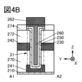
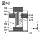
- 4A to 4D are cross-sectional views showing configuration examples of transistors.
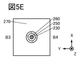
- 5A, 5D, and 5E are top views showing configuration examples of transistors.
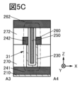
- 5B and 5C are cross-sectional views showing configuration examples of transistors.
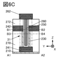
- 6A to 6C are cross-sectional views showing configuration examples of transistors.
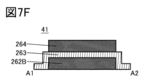
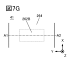
- FIG. 7A, 7C, 7E, and 7G are top views showing configuration examples of capacitors.
- 7B, 7D, 7F, and 7H are cross-sectional views showing configuration examples of capacitors.
- FIG. 8 is a cross-sectional view showing a configuration example of a semiconductor device.
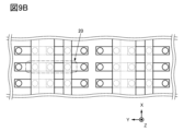
- 9A and 9B are top views showing configuration examples of the semiconductor device.
- FIG. 10A is a top view showing a configuration example of a semiconductor device.
- FIG. 10B is a cross-sectional view showing a configuration example of a semiconductor device.
- FIG. 10C is a circuit diagram for explaining the configuration of the semiconductor device.
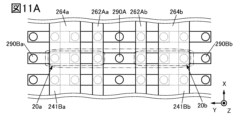
- 11A to 11C are top views showing configuration examples of semiconductor devices.
- FIG. 12A is a top view showing a configuration example of a semiconductor device.
- FIG. 12A is a top view showing a configuration example of a semiconductor device.
- FIG. 12B is a cross-sectional view showing a configuration example of a semiconductor device.
- FIG. 12C is a circuit diagram for explaining the configuration of the semiconductor device.
- FIG. 13A is a cross-sectional view showing a configuration example of a semiconductor device.
- FIG. 13B is a circuit diagram for explaining the configuration of the semiconductor device.
- 14A and 14B are cross-sectional views showing configuration examples of semiconductor devices.
- FIG. 15A is a top view showing a configuration example of a semiconductor device.
- FIG. 15B is a cross-sectional view showing a configuration example of a semiconductor device.
- FIG. 15C is a circuit diagram for explaining the configuration of the semiconductor device.
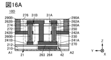
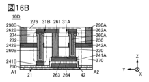
- 16A and 16B are cross-sectional views showing configuration examples of semiconductor devices.
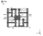
- FIG. 17A is a cross-sectional view showing a configuration example of a semiconductor device.
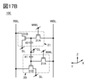
- FIG. 17B is a circuit diagram for explaining the configuration of the semiconductor device.
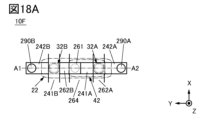
- FIG. 18A is a top view showing a configuration example of a semiconductor device.
- FIG. 18B is a cross-sectional view showing a configuration example of a semiconductor device.
- FIG. 18C is a circuit diagram for explaining the configuration of the semiconductor device.
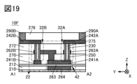
- FIG. 19 is a cross-sectional view showing a configuration example of a semiconductor device.
- 20A and 20D are top views showing configuration examples of transistors.
- 20B and 20C are cross-sectional views showing configuration examples of transistors.
- FIG. 21 is a cross-sectional view showing a configuration example of a transistor.
- FIG. 21 is a cross-sectional view showing a configuration example of a transistor.
- FIG. 22 is a cross-sectional view showing a configuration example of a semiconductor device.
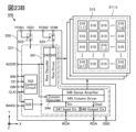
- 23A and 23B are diagrams illustrating an example of a storage device.
- FIG. 24 is a circuit diagram showing an example of a memory layer.
- FIG. 25 is a timing chart for explaining an operation example of the memory cell.
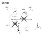
- 26A and 26B are circuit diagrams for explaining an operation example of the memory cell.
- 27A and 27B are circuit diagrams for explaining an operation example of the memory cell.
- FIG. 28 is a circuit diagram for explaining a configuration example of a semiconductor device.
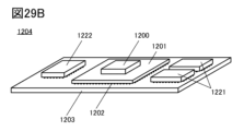
- 29A and 29B are diagrams showing an example of a semiconductor device.
- 30A and 30B are diagrams showing an example of an electronic component.
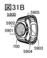
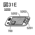
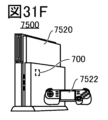
- 31A to 31J are diagrams illustrating examples of electronic devices.
- 32A to 32E are diagrams illustrating examples of electronic devices.
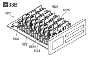
- 33A to 33C are diagrams illustrating examples of electronic devices.
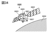
- FIG. 34 is a diagram showing an example of space equipment.
- the ordinal numbers “first” and “second” are used for convenience, and limit the number of constituent elements or the order of constituent elements (for example, the order of steps or the order of stacking). not something to do. Also, the ordinal number given to an element in one place in this specification may not match the ordinal number given to that element elsewhere in the specification or in the claims.
- film and “layer” can be interchanged depending on the case or situation.
- conductive layer can be changed to the term “conductive film.”
- insulating film can be changed to the term “insulating layer”.
- insulator can be replaced with an insulating film or an insulating layer.
- conductor can be replaced with a conductive film or a conductive layer.
- semiconductor can be interchanged with a semiconductor film or a semiconductor layer.
- oxynitride refers to a material whose composition contains more oxygen than nitrogen
- nitride oxide refers to a material whose composition contains more nitrogen than oxygen. point to the material.
- silicon oxynitride refers to a material whose composition contains more oxygen than nitrogen
- silicon nitride oxide refers to a material whose composition contains more nitrogen than oxygen. indicates
- equal in height indicates a configuration in which the height from a reference plane (for example, a flat plane such as a substrate surface) is equal in cross-sectional view.
- planarization processing typically CMP processing
- CMP processing may expose the surface of a single layer or multiple layers.
- the surfaces to be CMP-processed have the same height from the reference surface.
- the heights of the layers may differ depending on the processing apparatus, processing method, or material of the surface to be processed during CMP processing. In this specification and the like, this case is also treated as "matching heights".
- the height of the top surface of the first layer and the height of the second layer When the height difference from the upper surface of the layer is 20 nm or less, it is also said to be "matched in height".
- matching edges means that at least a part of the outline overlaps between the laminated layers when viewed from the top.
- the upper layer and the lower layer may be processed with the same mask pattern or partially with the same mask pattern.
- the outlines do not overlap, and the outline of the upper layer may be located inside the outline of the lower layer, or the outline of the upper layer may be located outside the outline of the lower layer. match.
- match includes both the case of complete match and the case of approximate match.
- One embodiment of the present invention relates to a semiconductor device provided over a substrate.
- a semiconductor device has a first transistor, a second transistor, and a capacitor, which can form a memory cell. Since a semiconductor device of one embodiment of the present invention includes memory cells, it has a function of storing data. Therefore, a semiconductor device of one embodiment of the present invention can be called a memory device.
- a semiconductor device of one embodiment of the present invention preferably includes a transistor (OS transistor) including a metal oxide in a channel formation region.
- the OS transistor has a small off current. Therefore, memory contents can be retained for a long time by using the OS transistor for a semiconductor device that can serve as a memory device.
- the refresh operation is not required or the frequency of the refresh operation is extremely low, the power consumption of the semiconductor device can be sufficiently reduced. Therefore, a semiconductor device with low power consumption can be provided.
- the OS transistor since the OS transistor has high frequency characteristics, the semiconductor device can read and write data at high speed. Therefore, a semiconductor device with high operating speed can be provided.
- the first transistor is provided in the same layer as the second transistor.
- Each of the first and second transistors has first to third conductors, a metal oxide, and an insulator.
- the second conductor is provided on the first conductor and has a region overlapping with the first conductor.
- the second conductor has an opening that overlaps with the first conductor when viewed from above.
- the metal oxide has regions in contact with the side surfaces of the opening of the second conductor and the top surface of the first conductor.
- the insulator is provided in the recess of the metal oxide.
- a third conductor is provided in the recess of the insulator.
- the third conductor has a region overlapping with the metal oxide through the insulator in a region between the first conductor and the second conductor in a cross-sectional view.
- the third conductor has a region facing the metal oxide via the insulator in a region between the first conductor and the second conductor in a cross-sectional view.
- the metal oxide has a region that functions as a channel formation region of the transistor.
- the first conductor has regions that function as one of the source and drain electrodes of the transistor.
- the second conductor has a region that functions as the other of the source and drain electrodes of the transistor.
- the third conductor has a region with a region that functions as the gate electrode of the transistor.
- the insulator has a region that functions as the gate insulator of the transistor.
- the channel length direction of the first and second transistors is the vertical direction.
- the first and second transistors are vertically structured transistors.
- a vertical transistor can be miniaturized. Therefore, by adopting a vertical structure for the first and second transistors, the transistors can be arranged at high density, and high integration in the semiconductor device can be realized.
- a transistor with a vertical structure is more likely to cause the electric field of the gate electrode to act on the entire channel formation region of the semiconductor layer. Therefore, the current density flowing through the transistor is increased, the on current of the transistor is increased, and the frequency characteristics can be improved.
- the first and second transistors when a memory cell is formed using first and second transistors, one of the first and second transistors functions as a writing transistor, and the other of the first and second transistors functions as a reading transistor. Function.
- the read transistor preferably has high on-current characteristics.
- the writing transistor preferably has low off-state current characteristics.
- the channel width related to the on-current of the transistor is adjusted by the size (also referred to as the diameter) of the opening in which a part of the component of the transistor is provided in a top view. can. Therefore, a memory device with excellent performance can be manufactured by making the opening provided with part of the components of the first transistor different from the opening provided with part of the components of the second transistor.
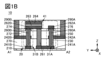
- FIG. 1A and 1B are a top view and a cross-sectional view, respectively, of a structure example of a semiconductor device of one embodiment of the present invention.
- FIG. 1A is a top view of the semiconductor device 10.
- FIG. 1B is a cross-sectional view of the semiconductor device 10, and is also a cross-sectional view of the portion indicated by the dashed-dotted line A1-A2 in FIG. 1A. Note that some elements are omitted in the top view of FIG. 1A for clarity of illustration.
- the semiconductor device 10 includes an insulator 210 on a substrate (not shown), a memory cell 20 on the insulator 210, a conductor 262A, a conductor 290A, a conductor 290B, and an insulator on the insulator 210. 270 , insulator 272 on insulator 270 , insulator 274 on insulator 272 , and insulator 276 on insulator 274 .
- Memory cell 20 is electrically connected to each of conductor 262A, conductor 290A, and conductor 290B.
- the memory cell 20 has a transistor 31A, a transistor 31B, a capacitor 41 on the transistor 31B, and a conductor 261. Note that the transistor 31A is provided in the same layer as the transistor 31B. Note that the components included in the semiconductor device of this embodiment may each have a single-layer structure or a laminated structure.
- the transistor 31 when describing items common to components distinguished by alphabets, reference numerals with alphabets omitted may be used.
- the transistor 31 may be referred to as a transistor 31 when describing items common to the transistor 31A and the transistor 31B.
- the direction parallel to the channel length direction of the illustrated transistor is the Z direction
- the direction perpendicular to the Z direction is the X direction
- the direction perpendicular to both the X direction and the Z direction is defined as the Y direction.
- the X direction and Y direction can be, for example, parallel to the substrate surface
- the Z direction can be perpendicular to the substrate surface.
- the transistor 31A has a conductor 241A, a conductor 242A, and a conductor 260A.
- Conductor 241A has a region that functions as one of the source and drain electrodes of transistor 31A
- conductor 242A has a region that functions as the other of the source and drain electrodes of transistor 31A
- conductor 260A has a region that functions as one of the source and drain electrodes of transistor 31A. has a region functioning as a gate electrode.
- the transistor 31B has a conductor 241B, a conductor 242B, and a conductor 260B.
- a conductor 241B has a region that functions as one of the source and drain electrodes of the transistor 31B
- a conductor 242B has a region that functions as the other of the source and drain electrodes of the transistor 31B
- a conductor 260B has a region that functions as the other of the source and drain electrodes of the transistor 31B. has a region functioning as a gate electrode.
- the capacitor 41 has a conductor 262B, an insulator 263, and a conductor 264.
- the conductor 262 B has a region that functions as one electrode of the capacitor 41
- the conductor 264 has a region that functions as the other electrode of the capacitor 41
- the insulator 263 has a region that functions as a dielectric of the capacitor 41 . have.
- the conductor 262B is electrically connected to the conductors 260B and 261, and the conductor 241A is electrically connected to the conductor 261. That is, the conductor 261 has a function of electrically connecting the conductor 262B and the conductor 241A.
- conductor 262B has a region that contacts the upper surface of each of conductors 260B and 261
- conductor 241A has a region that contacts the lower surface of conductor 261.
- the conductor 262A is electrically connected to the conductor 260A
- the conductor 290A is electrically connected to the conductor 242A
- the conductor 290B is electrically connected to the conductor 242B.
- conductor 262A has a region that contacts the top surface of conductor 260A
- conductor 290A has a region that contacts the top surface of conductor 242A
- conductor 290B has a region that contacts the top surface of conductor 242B.
- the transistor 31A is provided in the same layer as the transistor 31B. That is, the conductor 241A is provided in the same layer as the conductor 241B, and the conductor 242A is provided in the same layer as the conductor 242B. Specifically, the conductors 241 A and 241 B are provided over the insulator 210 , and the conductors 242 A and 242 B are provided over the insulator 270 .
- the conductor 262A is preferably formed from the same material and in the same process as the conductor 262B. By forming the conductor 262A using the same material and the same process as the conductor 262B, the number of steps in the manufacturing process of the semiconductor device can be reduced. At this time, conductor 262A has the same conductive material as conductor 262B. In addition, the conductor 262A is provided in the same layer as the conductor 262B. In FIG. 1B, conductor 262A and conductor 262B are provided on insulator 274. In FIG.
- FIG. 1A shows a configuration in which the conductors 241A, 242A, 242B, and 262B have the same length in the X direction.
- the present invention is not limited to this.
- the X-direction length of conductor 262B may be greater than the X-direction length of conductor 242B.
- the conductor 241B, the conductor 262A, and the conductor 264 have regions that function as wiring.
- Conductors 290A and 290B also have regions that function as plugs or wires.
- the direction in which the conductor 262A extends and the direction in which the conductor 290A extend are preferably different, and more preferably perpendicular to each other.
- the direction in which the conductor 241B extends and the direction in which the conductor 290B extends are preferably different, and more preferably perpendicular to each other.
- conductors 241B, 262A, and 264 are provided extending in the X direction.
- the direction in which the conductor 241B extends is the same as the direction in which the conductor 262A extends.
- the direction in which the conductor 241B extends is the same as the direction in which the conductor 264 extends.
- the direction in which the conductor 262A extends is the same as the direction in which the conductor 264 extends.
- the conductor 290A and the conductor 290B are provided extending in the Z direction.
- the direction in which the conductor 290A extends is the same as the direction in which the conductor 290B extends.
- the direction in which the conductor 262A extends is orthogonal to the direction in which the conductor 290A extends.
- the direction in which the conductor 241B extends is orthogonal to the direction in which the conductor 290B extends. Note that in this specification and the like, that the first direction is the same as the second direction can be rephrased as saying that the first direction is parallel to the second direction.
- FIG. 1B shows a configuration in which the conductors 290A and 290B are single layers.
- each of the conductors 290A and 290B may have a laminated structure.
- the insulators 276, 274, and 272 are used as the first conductors. It is preferable to provide the second conductor in contact with the inner wall of the provided opening, and to further provide the second conductor inside.
- the first conductor of the conductor 290A has a region that contacts the top surface of the conductor 242A, the side surface of the insulator 272, the side surface of the insulator 274, and the side surface of the insulator 276, respectively.
- the first conductor of the conductor 290B has regions in contact with the top surface of the conductor 242B, the side surfaces of the insulator 272, the side surfaces of the insulator 274, and the side surfaces of the insulator 276, respectively.
- the first conductor it is preferable to use a conductive material having a function of suppressing permeation of impurities such as water and hydrogen.
- the first conductor may have a single-layer structure or a laminated structure using one or more of tantalum, tantalum nitride, titanium, titanium nitride, ruthenium, and ruthenium oxide, for example. This can prevent water and impurities such as hydrogen from entering the metal oxide 230 through the conductors 290A and 290B.
- conductors 290A and 290B also function as wiring, conductors with high conductivity are preferably used.
- a conductive material containing tungsten, copper, or aluminum as a main component can be used for the second conductor.
- the first conductor comprises titanium and nitrogen
- the second conductor comprises tungsten
- the insulator 210 preferably functions as a barrier insulating film that prevents impurities such as water and hydrogen from diffusing from the substrate side into the transistor. Therefore, the insulator 210 has a function of suppressing the diffusion of impurities such as hydrogen atoms, hydrogen molecules, water molecules, nitrogen atoms, nitrogen molecules, nitrogen oxide molecules (N 2 O, NO, NO 2 and the like), and copper atoms. It is preferable to have an insulating material (that the impurities do not easily permeate). Alternatively, it is preferable to use an insulating material that has a function of suppressing the diffusion of oxygen (for example, at least one of oxygen atoms and oxygen molecules) (the oxygen hardly permeates).
- the insulator 210 preferably has a function of suppressing the diffusion of water, impurities such as hydrogen, and oxygen.
- silicon nitride, silicon nitride oxide, or the like can be used.
- silicon nitride which has a higher hydrogen barrier property, is preferably used as the insulator 210 .
- the insulator 210 preferably includes aluminum oxide, magnesium oxide, or the like, which has a high function of capturing and fixing hydrogen.
- water and impurities such as hydrogen can be prevented from diffusing into the transistor from the substrate side through the insulator 210 .
- diffusion of oxygen contained in the insulator 270 or the like to the substrate side can be suppressed.
- a barrier insulating film refers to an insulating film having barrier properties.
- the term "barrier property” refers to a function of suppressing diffusion of a corresponding substance (also referred to as low permeability).
- the corresponding substance has the function of capturing and fixing (also called gettering).
- the insulator 270, the insulator 272, the insulator 274, and the insulator 276 function as interlayer films.
- Insulator 270 , insulator 272 , insulator 274 , and insulator 276 each preferably have a lower dielectric constant than insulator 210 .
- the parasitic capacitance generated between wirings can be reduced.
- insulator 270, insulator 272, insulator 274, and insulator 276 may be silicon oxide, silicon oxynitride, fluorine-doped silicon oxide, carbon-doped silicon oxide, carbon- and nitrogen-doped oxide, respectively. It is preferable to include one or more of silicon and silicon oxide having vacancies.
- silicon oxide and silicon oxynitride are preferable because they are thermally stable.
- materials such as silicon oxide, silicon oxynitride, and silicon oxide having vacancies are preferable because a region containing oxygen released by heating can be easily formed.
- top surfaces of the insulators 270, 272, 274, and 276 may be planarized.
- the semiconductor device 10 can be used as a memory device.
- FIG. 1C shows a circuit diagram when the semiconductor device 10 is used as a memory device.
- the semiconductor device 10 can be rephrased as a memory device having memory cells 20 .
- the memory cell 20 has a transistor 31A, a transistor 31B, and a capacitor 41.
- FIG. 1C shows a circuit diagram when the semiconductor device 10 is used as a memory device.
- the semiconductor device 10 can be rephrased as a memory device having memory cells 20 .
- the memory cell 20 has a transistor 31A, a transistor 31B, and a capacitor 41.
- the gate electrode is electrically connected to the wiring WWL
- one of the source electrode and the drain electrode is electrically connected to one electrode of the capacitor 41
- the source electrode and the drain electrode are electrically connected to one electrode.
- the other is electrically connected to wiring WBL.
- a gate electrode is electrically connected to one electrode of the capacitor 41
- one of the source electrode and the drain electrode is electrically connected to the wiring SL
- the other of the source electrode and the drain electrode is electrically connected to the wiring RBL.
- connected to The other electrode of capacitor 41 is electrically connected to line CL.
- the wiring WWL functions as a write word line
- the wiring WBL functions as a write bit line
- the wiring RBL functions as a read bit line
- the wiring SL functions as a selection line
- the wiring CL functions as a capacitance line.
- the wiring WWL corresponds to the conductor 262A
- the wiring WBL corresponds to the conductor 290A
- the wiring RBL corresponds to the conductor 290B
- the wiring SL corresponds to the conductor 241B
- the wiring CL corresponds to the conductor 264. That is, conductor 262A has a region that functions as a write word line, conductor 290A has a region that functions as a write bit line, conductor 290B has a region that functions as a read bit line, and conductor 290B has a region that functions as a read bit line. 241B has a region that functions as a select line, and conductor 264 has a region that functions as a capacitance line.
- a memory device having memory cells will be described in detail in a later embodiment.
- FIG. 1A shows a configuration in which a straight line connecting the conductors 290A and 290B is perpendicular to the X direction.
- a straight line connecting the conductors 290A and 290B is parallel to the Y direction.
- the present invention is not limited to this.
- a straight line connecting conductors 290A and 290B may be inclined in the X direction.
- FIG. 1B can be referred to for the cross-sectional view of the portion indicated by the dashed-dotted line A1-A2 in FIG.
- FIG. 3A to 3D are top views and cross-sectional views showing configuration examples of transistors included in the memory cell 20.
- FIG. 3A is a top view of transistor 31.
- FIG. 3B is a cross-sectional view of the portion indicated by the dashed-dotted line A1-A2 in FIG. 3A
- FIG. 3C is a cross-sectional view of the portion indicated by the dashed-dotted line A3-A4 in FIG. 3A.
- FIG. 3D is a top view of the portion indicated by the dashed-dotted line B1-B2 in FIG. 3B. Note that some elements are omitted from the top views of FIGS. 3A and 3D for clarity of illustration.
- the transistor 31 includes a conductor 241 and an insulator 270 over the insulator 210, a metal oxide 230 over the conductor 241, an insulator 250 over the metal oxide 230, a conductor 260 over the insulator 250, A conductor 242 over insulator 270 and an insulator 272 over insulator 270 and conductor 242 .
- the conductor 241 has a region that functions as one of the source and drain electrodes of the transistor 31
- the conductor 242 has a region that functions as the other of the source and drain electrodes of the transistor 31
- the conductor 260 has a region that functions as the other of the source and drain electrodes of the transistor 31 .
- Metal oxide 230 has a region that functions as a channel forming region.
- a metal oxide that functions as a semiconductor (hereinafter also referred to as an oxide semiconductor) is preferably used for the metal oxide 230 .
- the bandgap of the metal oxide functioning as a semiconductor is preferably 2.0 eV or more, more preferably 2.5 eV or more.
- the off-state current of the transistor can be reduced by using a metal oxide with a large bandgap.
- metal oxide 230 it is preferable to use, for example, metal oxides such as indium oxide, gallium oxide, and zinc oxide. Moreover, as the metal oxide 230, it is preferable to use, for example, a metal oxide containing two or three elements selected from indium, the element M, and zinc.
- Element M includes gallium, aluminum, silicon, boron, yttrium, tin, copper, vanadium, beryllium, titanium, iron, nickel, germanium, zirconium, molybdenum, lanthanum, cerium, neodymium, hafnium, tantalum, tungsten, and magnesium.
- the element M is preferably one or more selected from aluminum, gallium, yttrium, and tin.
- a metal oxide containing indium, the element M, and zinc is sometimes referred to as an In-M-Zn oxide.
- the neighboring composition includes a range of ⁇ 30% of the desired atomic number ratio.
- the element M it is preferable to use gallium.
- the metal oxide 230 has a channel formation region and a source region and a drain region provided to sandwich the channel formation region in the transistor 31 . At least part of the channel formation region overlaps the conductor 260 . In other words, at least part of the channel forming region faces the conductor 260 .
- the source region overlaps one of the conductors 241 and 242 and the drain region overlaps the other of the conductors 241 and 242 . Note that the region overlapping with the conductor 242 can also be said to be a region facing the conductor 242 .
- a transistor including an oxide semiconductor when impurities and oxygen vacancies are present in a channel formation region in the oxide semiconductor, electrical characteristics are likely to fluctuate, and reliability may be degraded.
- hydrogen in the vicinity of oxygen vacancies may form defects in which hydrogen enters oxygen vacancies (hereinafter sometimes referred to as V OH ) to generate electrons serving as carriers. Therefore, if oxygen vacancies are included in the channel formation region in the oxide semiconductor, the transistor has normally-on characteristics (a channel exists even if no voltage is applied to the gate electrode, and a current flows through the transistor). easy to become. Therefore, impurities, oxygen vacancies, and VOH are preferably reduced as much as possible in the channel formation region in the oxide semiconductor.
- an insulator containing oxygen that is released by heating (hereinafter sometimes referred to as excess oxygen) is provided in the vicinity of the oxide semiconductor, and heat treatment is performed so that the oxide semiconductor is converted from the insulator.
- Oxygen can be supplied to reduce oxygen vacancies and VOH .
- the on-state current or the field-effect mobility of the transistor might be lowered.
- variations in the amount of oxygen supplied to the source region or the drain region within the substrate surface cause variations in the characteristics of the semiconductor device having transistors.
- the channel formation region is a high-resistance region with a low carrier concentration because it has less oxygen vacancies or a lower impurity concentration than the source and drain regions. Therefore, the channel forming region can be said to be i-type (intrinsic) or substantially i-type.
- the carrier concentration of the channel formation region is 1 ⁇ 10 18 cm ⁇ 3 or less, less than 1 ⁇ 10 17 cm ⁇ 3 , less than 1 ⁇ 10 16 cm ⁇ 3 , less than 1 ⁇ 10 15 cm ⁇ 3 , and 1 ⁇ 10 14 .
- cm ⁇ 3 less than 1 ⁇ 10 13 cm ⁇ 3 , less than 1 ⁇ 10 12 cm ⁇ 3 , less than 1 ⁇ 10 11 cm ⁇ 3 , or less than 1 ⁇ 10 10 cm ⁇ 3 .
- the lower limit of the carrier concentration in the channel forming region is not particularly limited, but can be, for example, 1 ⁇ 10 ⁇ 9 cm ⁇ 3 .
- the impurity concentration in the metal oxide 230 is lowered to lower the defect level density.
- a low impurity concentration and a low defect level density are referred to as high-purity intrinsic or substantially high-purity intrinsic.
- an oxide semiconductor (or metal oxide) with a low carrier concentration is sometimes referred to as a highly purified intrinsic or substantially highly purified intrinsic oxide semiconductor (or metal oxide).
- the impurities in the metal oxide 230 refer to, for example, substances other than the main components that constitute the metal oxide 230.
- an element with a concentration of less than 0.1 atomic percent can be considered an impurity.
- impurities in the metal oxide 230 include hydrogen, nitrogen, alkali metals, alkaline earth metals, iron, nickel, silicon, and the like.
- the source region and the drain region are low-resistance regions with high carrier concentration because they have many oxygen vacancies or have a high impurity concentration. That is, the source region and the drain region are n-type regions (low resistance regions) having a higher carrier concentration than the channel forming region.
- the concentrations of the metal element and the impurity element detected in each region are not limited to stepwise changes for each region, and may change continuously within each region. That is, the concentration of the impurity element may be decreased in a region closer to the channel formation region.
- Reducing the impurity concentration in the metal oxide 230 is effective in stabilizing the electrical characteristics of the transistor. Moreover, in order to reduce the impurity concentration of the metal oxide 230, it is preferable to reduce the impurity concentration in adjacent films as well.
- An opening reaching the conductor 241 is provided in the insulator 272 , the conductor 242 , and the insulator 270 .
- the opening has a region overlapping with the conductor 241 in top view.
- at least part of each of the metal oxide 230, the insulator 250, and the conductor 260 is disposed in the opening.
- the opening can be said to include the opening of the insulator 272 , the opening of the conductor 242 , and the opening of the insulator 270 .
- the conductor 242 has an opening that overlaps with the conductor 241 when viewed from above.
- the metal oxide 230 is provided in contact with the insulator 272 , the conductor 242 , and the side and bottom surfaces of the opening provided in the insulator 270 .
- the metal oxide 230 has regions in contact with the side surfaces of the opening of the conductor 242 and the top surface of the conductor 241 .
- the metal oxide 230 has a region in contact with the top surface of the insulator 272 .
- the metal oxide 230 has recesses. The recess has a region that overlaps with the opening of the conductor 242 when viewed from above.
- At least part of the insulator 250 is provided in the recess of the metal oxide 230 .
- Insulator 250 also has a region in contact with the top surface of metal oxide 230 .
- Insulator 250 also has a recess. The recess is located inside the recess of the metal oxide 230 .
- the conductor 260 is provided so as to fill the recess of the insulator 250 . Also, the conductor 260 has a region in contact with the top surface of the insulator 250 . In addition, the conductor 260 has a region overlapping with the metal oxide 230 with the insulator 250 interposed therebetween in a region between the conductor 241 and the conductor 242 in a cross-sectional view. In other words, the conductor 260 has a region facing the metal oxide 230 with the insulator 250 interposed therebetween in a region between the conductors 241 and 242 in a cross-sectional view.
- the channel length of the transistor 31 is the shortest distance (L1 in FIG. 3B) from the top surface of the conductor 241 to the bottom surface of the conductor 242 in a cross-sectional view. is also the film thickness of In other words, the channel length of the transistor 31 can be adjusted by the thickness of the insulator 270 in the region overlapping with the conductor 241 . For example, by reducing the thickness of the insulator 270, the transistor 31 with a short channel length can be manufactured.
- the channel width of the transistor 31 is the length of the region where the insulator 270 and the metal oxide 230 are in contact with each other when viewed from the top, and the length of the outline (periphery) of the metal oxide 230 when viewed from the top. be.
- the channel width of the transistor 31 can be adjusted by the diameter of the opening provided in the insulator 270 .
- the opening can be referred to as an opening in which some of the components of the transistor 31 (here, the metal oxide 230, the insulator 250, and the conductor 260) are provided.
- the transistor 31 has a structure in which a channel forming region surrounds a gate electrode. Therefore, the transistor 31 can be said to have a CAA (Channel-All-Around) structure.
- FIG. 3D shows a configuration in which the top surface shape of the opening of the conductor 242 has a circular shape
- the present invention is not limited to this.
- the top surface shape of the opening of the conductor 242 may be elliptical, polygonal, or polygonal with rounded corners.
- polygonal shapes refer to triangles, quadrilaterals, pentagons, hexagons, and the like.
- An insulator 274 is provided over the insulator 272 , and a conductor 262 is provided over the insulator 274 and the conductor 260 .
- a crystalline oxide semiconductor is preferably used for the metal oxide 230 .
- crystalline oxide semiconductors include a CAAC-OS (c-axis aligned crystalline oxide semiconductor), an nc-OS (nanocrystalline oxide semiconductor), a polycrystalline oxide semiconductor, a single-crystalline oxide semiconductor, and the like.
- CAAC-OS or nc-OS is preferably used as the metal oxide 230, and CAAC-OS is particularly preferably used.
- CAAC-OS is a metal oxide that has a dense structure with high crystallinity and few impurities and defects (for example, oxygen vacancies).
- heat treatment is performed at a temperature at which the metal oxide is not polycrystallized (for example, 400° C. or more and 600° C. or less), so that the CAAC-OS has a dense structure with higher crystallinity.
- a temperature at which the metal oxide is not polycrystallized for example, 400° C. or more and 600° C. or less
- the metal oxide 230 by using a crystalline oxide such as CAAC-OS as the metal oxide 230 , extraction of oxygen from the metal oxide 230 by the conductors 241 and 242 can be suppressed. As a result, oxygen can be suppressed from being extracted from the metal oxide 230 even when heat treatment is performed, so the transistor is stable against high temperatures (so-called thermal budget) in the manufacturing process. Further, a decrease in the conductivity of the conductors 241 and 242 can be suppressed.
- a crystalline oxide such as CAAC-OS
- the nc-OS has periodicity in the atomic arrangement in a minute region (for example, a region of 1 nm or more and 10 nm or less, particularly a region of 1 nm or more and 3 nm or less).
- the nc-OS has minute crystals (also referred to as nanocrystals).
- the nc-OS since there is no regularity in crystal orientation between different nanocrystals, no orientation is observed in the entire film. That is, when the nc-OS is used as the metal oxide 230, the film characteristics of the metal oxide 230 are constant regardless of the direction of carriers flowing through the metal oxide 230, and thus the electrical characteristics of the transistor are stable.
- the metal oxide 230 is CAAC-OS, nc-OS, pseudo-amorphous oxide semiconductor (a-like OS), amorphous oxide semiconductor, polycrystalline oxide semiconductor, CAC-OS (cloud-aligned composite oxide semiconductor) may have two or more kinds.
- the position of the peak indicating the c-axis orientation may vary depending on the type and composition of the metal elements forming the CAAC-OS.
- a plurality of bright points (spots) are observed in the electron beam diffraction pattern of the CAAC-OS film. A certain spot and another spot are observed at point-symmetrical positions with respect to the spot of the incident electron beam that has passed through the sample (also referred to as a direct spot) as the center of symmetry.
- an electron beam diffraction pattern is obtained in which a plurality of spots are observed within a ring-shaped area centered on the spot.
- the metal oxide 230 can be rephrased as a semiconductor layer including the channel formation region of the transistor 31 .
- a material that can be used for the semiconductor layer is not limited to a metal oxide that functions as a semiconductor (an oxide semiconductor).
- a semiconductor such as single crystal silicon, polycrystalline silicon, or amorphous silicon may be used as the semiconductor layer, and for example, low temperature poly silicon (LTPS) may be used.
- LTPS low temperature poly silicon
- a transition metal chalcogenide that functions as a semiconductor may be used as the semiconductor layer.
- MoTe 2 tungsten sulfide
- tungsten selenide typically WSe 2
- tungsten tellurium typically WTe 2
- hafnium sulfide typically HfS 2
- hafnium selenide typically HfSe 2
- zirconium sulfide typically ZrS 2
- zirconium selenide typically ZrSe 2
- ZrSe 2 zirconium selenide
- the insulator 250 may have a single-layer structure or a laminated structure.
- the insulator 250 for example, silicon oxide, silicon oxynitride, silicon oxide to which fluorine is added, silicon oxide to which carbon is added, silicon oxide to which carbon and nitrogen are added, silicon oxide having vacancies, or the like can be used.
- silicon oxide and silicon oxynitride are preferable because they are stable against heat.
- the insulator 250 contains at least oxygen and silicon.
- the concentration of impurities such as water and hydrogen in the insulator 250 is preferably reduced.
- an insulator having a barrier property against oxygen may be provided between the insulator 250 and the metal oxide 230 .
- the insulator is provided in contact with the lower surface of the insulator 250 and the concave portion of the metal oxide 230 . Since the insulator has a barrier property against oxygen, oxygen contained in the insulator 250 can be supplied to the channel formation region, and excessive supply of oxygen contained in the insulator 250 to the channel formation region can be suppressed. Therefore, when heat treatment or the like is performed, desorption of oxygen from the metal oxide 230 can be suppressed, and formation of oxygen vacancies in the metal oxide 230 can be suppressed. Therefore, the electrical characteristics of the transistor 31 can be improved, and the reliability can be improved.
- An insulator containing oxides of one or both of aluminum and hafnium is preferably used as the insulator.
- the insulator aluminum oxide, hafnium oxide, an oxide containing aluminum and hafnium (hafnium aluminate), an oxide containing hafnium and silicon (hafnium silicate), or the like can be used. It is more preferable to use aluminum oxide as the insulator.
- the insulator contains at least oxygen and aluminum. Note that the insulator should be less permeable to oxygen than the insulator 250, for example.
- a material that is less permeable to oxygen than the insulator 250 may be used, for example.
- magnesium oxide, gallium oxide, gallium zinc oxide, indium gallium zinc oxide, or the like may be used as the insulator.
- FIG. 3B shows a configuration in which the conductor 260 is a single layer.
- the conductor 260 may have a laminated structure.
- conductor 260 preferably has a first conductor and a second conductor over the first conductor.
- the first conductor of conductor 260 is preferably arranged to wrap the bottom and side surfaces of the second conductor of conductor 260 .
- a conductive material having a function of suppressing diffusion of impurities such as hydrogen atoms, hydrogen molecules, water molecules, nitrogen atoms, nitrogen molecules, nitrogen oxide molecules, or copper atoms is used.
- impurities such as hydrogen atoms, hydrogen molecules, water molecules, nitrogen atoms, nitrogen molecules, nitrogen oxide molecules, or copper atoms is preferred.
- a conductive material having a function of suppressing diffusion of oxygen eg, at least one of oxygen atoms and oxygen molecules
- the second conductor of the conductor 260 is oxidized by oxygen contained in the insulator 250, for example, and the conductivity is lowered. can be suppressed.
- the conductive material having a function of suppressing diffusion of oxygen titanium, titanium nitride, tantalum, tantalum nitride, ruthenium, ruthenium oxide, or the like is preferably used, for example.
- the conductor 260 use a conductor with high conductivity.
- the second conductor of conductor 260 can use a conductive material whose main component is tungsten, copper, or aluminum.
- the second conductor of the conductor 260 may have a layered structure, for example, a layered structure of titanium or titanium nitride and any of the above conductive materials.
- an insulator having a barrier property against hydrogen may be provided between the insulator 250 and the conductor 260 .
- impurities such as hydrogen contained in the conductor 260 can be prevented from diffusing into the insulator 250 and the metal oxide 230 .
- Silicon nitride for example, may be used as the insulator.
- the insulator contains at least nitrogen and silicon.
- aluminum oxide, magnesium oxide, hafnium oxide, gallium oxide, indium gallium zinc oxide, silicon nitride oxide, or the like may be used.
- the insulator may be less permeable to hydrogen than the insulator 250, for example.
- a material that is less permeable to hydrogen than the insulator 250 may be used, for example.
- An insulator having a barrier property against oxygen may be provided between the insulator 250 and the conductor 260 .
- diffusion of oxygen contained in the insulator 250 to the conductor 260 can be suppressed.
- reduction in the amount of oxygen supplied to the metal oxide 230 can be suppressed.
- oxidation of the conductor 260 due to oxygen contained in the insulator 250 can be suppressed.
- An insulator containing oxides of one or both of aluminum and hafnium is preferably used as the insulator.
- the insulator aluminum oxide, hafnium oxide, an oxide containing aluminum and hafnium (hafnium aluminate), an oxide containing hafnium and silicon (hafnium silicate), or the like can be used.
- Hafnium oxide is more preferably used as the insulator.
- the insulator contains at least oxygen and hafnium.
- Hafnium oxide is suitable because it has a barrier property against hydrogen.
- Metal oxide 230, insulator 250, and conductor 260 are formed in insulator 272, conductor 242, and openings provided in insulator 270 by atomic layer deposition (ALD).
- ALD atomic layer deposition
- the ALD method includes a thermal ALD (thermal ALD) method in which reaction of a precursor and a reactant is performed only with thermal energy, a PEALD (plasma enhanced ALD) method using a plasma-excited reactant, and the like.
- PEALD plasma enhanced ALD
- film formation can be performed at a lower temperature by using plasma, which is preferable in some cases.
- the ALD method can deposit atoms one layer at a time, it is possible to deposit ultra-thin films, to form films with high aspect ratio structures, to form films with few defects such as pinholes, and to improve coverage. It has effects such as enabling excellent film formation and enabling film formation at a low temperature. Therefore, the metal oxide 230, the insulator 250, and the conductor 260 can be deposited on the side surfaces of the openings provided in the insulator 272, the conductor 242, and the insulator 270 with good coverage.
- a film formed by the ALD method may contain more impurities such as carbon than films formed by other film forming methods.
- quantification of impurities can be performed using secondary ion mass spectrometry (SIMS: Secondary Ion Mass Spectrometry), X-ray photoelectron spectroscopy (XPS: X-ray Photoelectron Spectroscopy), or Auger electron spectroscopy (AES: Auger Electron Spectroscopy) can be performed using
- microwave treatment after forming a metal oxide film using the ALD method, and it is more preferable to perform microwave treatment in an atmosphere containing oxygen.
- oxygen gas By performing microwave treatment in an oxygen-containing atmosphere, oxygen gas can be plasmatized using high frequencies such as microwaves and RF, and the oxygen plasma can act on metal oxides. At this time, it is also possible to irradiate the metal oxide with high frequency waves such as microwaves and RF. That is, the metal oxide can be acted on by microwaves, high frequencies such as RF, oxygen plasma, and the like.
- the impurity concentration of the metal oxide can be reduced by the action of high frequency, oxygen plasma, or the like.
- hydrogen in the metal oxide can be released as water molecules.
- carbon in the metal oxide can be desorbed as oxocarbon (CO and/or CO 2 ).
- oxygen vacancies, VOH , and the like in the metal oxide can be reduced by supplying oxygen radicals generated by oxygen plasma to the metal oxide.
- the atoms in the metal oxide are given energy higher than the processing temperature of the microwave treatment. Therefore, the rearrangement of the metal atoms and oxygen atoms in the metal oxide is promoted, and the crystallinity of the metal oxide can be improved. Note that the crystallinity of the metal oxide tends to improve as the impurity concentration and the amount of defects (oxygen vacancies, VOH , etc.) in the metal oxide are reduced. In other words, microwave treatment in an oxygen-containing atmosphere reduces the impurity concentration and the amount of defects in the metal oxide and improves the crystallinity of the metal oxide.
- the insulator 270 is, for example, an oxide containing silicon such as silicon oxide, silicon oxynitride, fluorine-added silicon oxide, carbon-added silicon oxide, carbon- and nitrogen-added silicon oxide, or silicon oxide having vacancies. is preferably used.
- silicon oxide and silicon oxynitride are preferable because they are thermally stable.
- a material such as silicon oxide, silicon oxynitride, or silicon oxide having vacancies is preferable because a region containing excess oxygen can be easily formed.
- the metal oxide 230 in the region in contact with the insulator 270 functions as a channel formation region; or substantially i-type.
- insulator 270 preferably comprises silicon oxide or an oxide containing silicon, such as silicon oxynitride.
- the conductors 241 and 242 it is preferable to use a conductive material that is difficult to oxidize or a conductive material that has a function of suppressing the diffusion of oxygen.
- the conductive material include a conductive material containing nitrogen and a conductive material containing oxygen. By using the conductive material, a decrease in the conductivity of the conductors 241 and 242 can be suppressed.
- each of the conductors 241 and 242 contains at least metal and nitrogen.
- nitrides containing tantalum for example, nitrides containing titanium, nitrides containing molybdenum, nitrides containing tungsten, nitrides containing tantalum and aluminum, titanium, and aluminum are used, respectively. It is preferable to use a nitride or the like containing In one aspect of the present invention, nitrides containing tantalum are particularly preferred.
- ruthenium oxide, ruthenium nitride, an oxide containing strontium and ruthenium, an oxide containing lanthanum and nickel, or the like may be used. These materials are preferable because they are conductive materials that are difficult to oxidize or materials that maintain conductivity even after absorbing oxygen.
- FIG. 3B shows a configuration in which the conductors 241 and 242 are single layers.
- each of the conductors 241 and 242 may have a laminated structure.
- each of the conductors 241 and 242 may have a two-layer structure of a first conductor and a second conductor.
- a conductive material that is difficult to oxidize or a conductive material that has a function of suppressing diffusion of oxygen is preferably used as the first conductor in contact with the insulator 270. Accordingly, a decrease in the conductivity of the conductors 241 and 242 can be suppressed.
- the second conductors of the conductors 241 and 242 preferably have higher conductivity than the first conductors of the conductors 241 and 242 . Further, it is preferable that the thickness of the second conductors of the conductors 241 and 242 be larger than the thickness of the first conductors of the conductors 241 and 242 .
- tantalum nitride or titanium nitride can be used as the first conductors of the conductors 241 and 242, and tungsten can be used as the second conductors of the conductors 241 and 242.
- an insulator having a barrier property against oxygen is preferably provided between the conductor 241 and the insulator 270 in order to suppress oxidation of the conductor 241 by oxygen contained in the insulator 270 .
- an insulator having a barrier property against oxygen is preferably provided between the conductor 242 and the insulator 270 in order to suppress oxidation of the conductor 242 due to oxygen contained in the insulator 270 .
- An insulator containing an oxide of one or both of aluminum and hafnium is preferably used as the insulator.
- aluminum oxide, hafnium oxide, an oxide containing aluminum and hafnium (hafnium aluminate), an oxide containing hafnium and silicon (hafnium silicate), or the like can be used.
- the ends of the conductor 260 coincide with the respective ends of the metal oxide 230 and the insulator 250, as shown in FIG. 3B.
- the edges of the conductor 260 may not be aligned with the edges of the metal oxide 230 and the insulator 250 .
- a portion of conductor 260 is removed.
- the end of conductor 260 coincides with the end of conductor 262 .
- FIG. 3B shows a configuration in which the conductor 241 does not have a recess in the region overlapping the opening of the insulator 270 .
- the conductor 241 may have recesses in regions overlapping the openings. In other words, a portion of the upper surface of the conductor 241 overlapping the opening may be removed. Since the conductor 241 has a recess in a region overlapping with the opening, the end of the region (the facing region) where the metal oxide 230 and the conductor 260 overlap with the insulator 250 interposed therebetween can be brought closer to the conductor 241. can be done.
- the conductor 260 can have a region that overlaps (faces with) the conductor 241 with the metal oxide 230 and the insulator 250 interposed therebetween.
- a region where the metal oxide 230 and the conductor 260 do not overlap with each other with the insulator 250 interposed therebetween (region where they do not face each other), that is, a so-called Loff region is narrowed or provided. can be configured without Therefore, the frequency characteristic of transistor 31 can be improved.
- the write speed and read speed of the memory cell 20 can be improved, and the operating speed of the semiconductor device 10 can be improved. Therefore, a semiconductor device with high operating speed can be provided.
- the conductor 241 may have an opening that overlaps with the opening of the insulator 270 and reaches the insulator 210 .
- a region of the conductor 241 that overlaps the opening of the insulator 270 may be removed. Since the conductor 241 has an opening that reaches the insulator 210 , an end portion of a region where the metal oxide 230 and the conductor 260 overlap (face each other) with the insulator 250 interposed therebetween can be brought closer to the conductor 241 . can.
- the conductor 260 can have a region that overlaps (faces with) the conductor 241 with the metal oxide 230 and the insulator 250 interposed therebetween. Therefore, the frequency characteristic of transistor 31 can be improved.
- FIG. 3B shows a configuration in which the metal oxide 230 has a region in contact with the top surface of the insulator 272 .
- the present invention is not limited to this.
- insulator 272 may not be provided, as shown in FIG. 4D.
- the metal oxide 230 has regions in contact with part of the top surface of the conductor 242 and the side surfaces of the opening of the conductor 242 .
- the contact area between the metal oxide 230 and the conductor 242 can be increased, and the on-state current of the transistor 31 can be increased. Therefore, a semiconductor device with large on-current can be provided.
- FIGS. 5A-5E show a transistor having a different configuration than the transistor 31 shown in FIGS. 3A-3D.
- FIGS. 5A to 5E are top views and cross-sectional views showing another configuration example of the transistor 31.
- FIG. 5A, 5D, and 5E are top views of transistor 31.
- FIG. 5B is a cross-sectional view of the portion indicated by the dashed-dotted line A1-A2 in FIG. 5A
- FIG. 5C is a cross-sectional view of the portion indicated by the dashed-dotted line A3-A4 in FIG. 5A
- 5D is a top view of the portion indicated by the dashed-dotted line B1-B2 in FIG. 5B
- FIG. 5E is a top view of the portion indicated by the dashed-dotted line B3-B4 in FIG. 5B.
- some elements are omitted for clarity of illustration.
- a transistor 31 shown in FIGS. 5A to 5E is a modification of the transistor 31 shown in FIGS. 3A to 3D.
- the transistor 31 shown in FIGS. 5A-5E differs from the transistor 31 shown in FIGS. 3A-3D in the shape of the metal oxide 230, the insulator 250, and the conductor 260.
- FIG. hereinafter, portions different from the transistor 31 shown in FIGS. 3A to 3D will mainly be described, and descriptions of overlapping portions will be omitted.
- the diameters of the openings of the insulator 272 and the conductor 242 are smaller than the diameter of the opening of the insulator 270 .
- the metal oxide 230 is provided in contact with the side and bottom surfaces of the opening of the insulator 270 . At this time, the top surface of the metal oxide 230 has a region that matches the top surface of the insulator 270 and contacts the bottom surface of the conductor 242 .
- the insulator 250 is provided in openings of the insulator 272 and the conductor 242 and in recesses of the metal oxide 230 .
- the insulator 250 has regions in contact with the side surfaces of the opening of the insulator 272 and the side surfaces of the opening of the conductor 242 .
- the top surface of insulator 250 coincides with the respective top surfaces of conductor 260 and insulator 272 .
- the conductor 260 is provided so as to fill the recess of the insulator 250 .
- Conductor 260 has a region that contacts the lower surface of conductor 262 .
- the structure shown in FIGS. 5A to 5E forms the metal oxide 230 in the opening of the insulator 270, and the insulating material is formed in the opening of the insulator 272, the opening of the conductor 242, and the recess of the metal oxide 230.
- An insulating film to be the body 250 and a conductive film to be the conductor 260 are formed, and planarization is performed until the top surface of the insulator 272 is exposed.
- CMP chemical mechanical polishing
- the metal oxide 230 is provided below the insulator 272 and therefore does not come into contact with the conductor 262 on the insulator 272 . Therefore, the metal oxide 230 can function as a channel formation region of the transistor 31 . Further, compared with the transistor 31 shown in FIGS. 3A to 3D, the transistor 31 shown in FIGS. 5A to 5E can form the insulator 250 and the conductor 260 without using a photolithography method. Therefore, it is possible to achieve a reduction in size or a high degree of integration. In addition, since the insulator 274 is not required, the number of steps in manufacturing the semiconductor device can be reduced.
- FIG. 5B shows a configuration in which the conductor 241 does not have a recess in the region overlapping the opening of the insulator 270 .
- the present invention is not limited to this.
- the conductor 241 may have recesses in regions overlapping the openings. In other words, a portion of the upper surface of the conductor 241 overlapping the opening may be removed.
- conductor 241 may have an opening that overlaps the opening and reaches insulator 210 . In other words, a region of the conductor 241 that overlaps the opening of the insulator 270 may be removed.
- the conductor 241 has a recessed portion or an opening in a region overlapping with the opening of the insulator 270, so that the end portion of the region (the facing region) where the metal oxide 230 and the conductor 260 overlap with the insulator 250 interposed therebetween. , can be brought closer to the conductor 241 . Therefore, the frequency characteristic of transistor 31 can be improved.
- FIG. 5B shows a configuration in which the metal oxide 230 has recesses.
- metal oxide 230 may have openings down to conductors 241, as shown in FIG. 6C.
- the metal oxide 230 may have a hollow cylindrical shape.
- the conductor 241 has a recessed portion or an opening in a region overlapping with the opening of the insulator 270, as in FIGS. 6A and 6B. good too.
- the contact area between the conductor 241 and the metal oxide 230 can be increased, and the on-state current of the transistor 31 can be increased.
- FIG. 7A and 7B are a top view and a cross-sectional view showing a configuration example of the capacitor 41 of the memory cell 20.
- FIG. 7A is a top view of the capacitor 41.
- FIG. 7B is a cross-sectional view of the portion indicated by the dashed-dotted line A1-A2 in FIG. 7A. Note that some elements are omitted in the top view of FIG. 7A for clarity of illustration.
- the capacitor 41 has a conductor 262B, an insulator 263 on the conductor 262B, and a conductor 264 on the insulator 263.
- the conductor 262 B has a region that functions as one electrode of the capacitor 41
- the conductor 264 has a region that functions as the other electrode of the capacitor 41
- the insulator 263 has a region that functions as a dielectric of the capacitor 41 .
- the capacitor 41 constitutes an MIM (Metal-Insulator-Metal) capacitor.
- the conductor 264 is provided extending outside the end of the conductor 262B in the X direction. 7A and 7B, the Y-direction end of the conductor 262B coincides with the Y-direction end of the insulator 263 and the conductor 264, respectively.
- the conductor 262B and the conductor 264 may each have a single-layer structure or a laminated structure.
- Each of conductor 262B and conductor 264 may have a first conductor and a second conductor on the first conductor. Note that one or both of the conductor 262B and the conductor 264 may be stacked in the opposite order.
- a conductor that can be used as the first conductors of the conductors 241 and 242 may be used as the first conductors of the conductors 262B and 264 .
- a conductor that can be used as the second conductors of the conductors 241 and 242 may be used.
- titanium nitride can be used as the first conductor of the conductor 262B and the conductor 264
- tungsten can be used as the second conductor of the conductor 262B and the conductor 264.
- a high dielectric constant (high-k) material (high dielectric constant material) is preferably used for the insulator 263 .
- the insulator 263 is preferably formed by a film formation method with good coverage, such as an ALD method or a CVD method.
- high dielectric constant (high-k) materials examples include oxides, oxynitrides, nitride oxides, and nitrides containing one or more metal elements selected from aluminum, hafnium, zirconium, gallium, and the like. be done.
- silicon may be contained in the above oxide, oxynitride, nitride oxide, or nitride. Insulators made of the above materials can also be laminated and used.
- high dielectric constant (high-k) materials include aluminum oxide, hafnium oxide, zirconium oxide, oxides containing aluminum and hafnium, oxynitrides containing aluminum and hafnium, oxides containing silicon and hafnium, Oxynitrides with silicon and hafnium, oxides with silicon and zirconium, oxynitrides with silicon and zirconium, oxides with hafnium and zirconium, and oxynitrides with hafnium and zirconium.
- the insulator 263 can be thick enough to suppress leakage current and the capacitance of the capacitor 41 can be sufficiently secured.
- a laminated insulator composed of the above materials, and a laminated structure of a high dielectric constant (high-k) material and a material having a higher dielectric strength than the high dielectric constant (high-k) material is used.
- high-k high dielectric constant
- high-k high dielectric constant
- an insulator in which zirconium oxide, aluminum oxide, and zirconium oxide are stacked in this order can be used as the insulator 263 .
- an insulator in which zirconium oxide, aluminum oxide, zirconium oxide, and aluminum oxide are stacked in this order can be used.
- an insulating film in which hafnium zirconium oxide, aluminum oxide, hafnium zirconium oxide, and aluminum oxide are stacked in this order can be used.
- an insulator having a relatively high dielectric strength, such as aluminum oxide the dielectric strength is improved and electrostatic breakdown of the capacitor 41 can be suppressed.
- 7A and 7B show a configuration in which the Y-direction end of the conductor 262B matches the Y-direction end of the insulator 263 and the conductor 264, respectively.
- the present invention is not limited to this.
- FIGS. 7C and 7D are a top view and a cross-sectional view showing another configuration example of the capacitor 41.
- FIG. 7C is a top view of capacitor 41.
- FIG. FIG. 7D is a cross-sectional view of the portion indicated by the dashed-dotted line A1-A2 in FIG. 7C.
- the Y-direction end of the conductor 262B may be located outside the Y-direction ends of the conductor 264 and the insulator 263, respectively.
- FIG. 7D shows a configuration in which the end of the conductor 264 in the Y direction coincides with the end of the insulator 263 in the Y direction, but the present invention is not limited to this.
- the Y-direction end of the conductor 264 may be located inside the Y-direction end of the insulator 263 .
- FIG. 7E and 7F are a top view and a cross-sectional view showing another configuration example of the capacitor 41.
- FIG. 7E is a top view of capacitor 41.
- FIG. FIG. 7F is a cross-sectional view of the portion indicated by the dashed-dotted line A1-A2 in FIG. 7E.
- the insulator 263 may be provided to cover the top and side surfaces of the conductor 262B.
- FIG. 7F shows a configuration in which the insulator 263 is in contact with the side and top surfaces of the conductor 262B. With this structure, the insulator 263 can sufficiently separate the conductor 264 and the conductor 262B.
- FIG. 7F shows a configuration in which the Y-direction end of the conductor 264 coincides with the Y-direction end of the conductor 262B.
- the present invention is not limited to this.
- FIG. 7G and 7H are a top view and a cross-sectional view showing another configuration example of the capacitor 41.
- FIG. 7G is a top view of capacitor 41.
- FIG. FIG. 7H is a cross-sectional view of the portion indicated by the dashed-dotted line A1-A2 in FIG. 7G.
- the Y-direction end of the conductor 264 may be located outside the Y-direction end of the conductor 262B.
- the outer circumference of the conductor 262B is located inside the outer circumference of the conductor 264 in top view.
- the Y-direction end of the conductor 264 may be located inside the Y-direction end of the conductor 262B.
- FIG. 1B shows a configuration in which the capacitor 41 has a planar shape. In other words, a configuration in which the capacitor 41 is provided on the insulator 274 is shown.
- the present invention is not limited to this.
- FIG. 8 shows a cross-sectional view of a semiconductor device different from the semiconductor device 10 shown in FIG. 1B. Note that FIG. 1A can be referred to for the top view of the semiconductor device illustrated in FIG.
- the semiconductor device shown in FIG. 8 differs from the semiconductor device 10 shown in FIG. 1B in the configuration and shape of the capacitor 41 .
- the semiconductor device shown in FIG. 8 also differs from the semiconductor device 10 shown in FIG. 1B in that it does not have the conductor 262B.
- a portion of the capacitor 41 may be positioned within openings provided in the insulators 274, 272, and 270.
- the capacitor 41 has a conductor 261 , an insulator 263 over the conductor 261 , and a conductor 264 over the insulator 263 .
- the conductor 261 has a region in contact with the side and bottom surfaces of the opening, a region in contact with the top surface of the conductor 260B, and a region in contact with part of the top surface of the insulator 274 .
- the conductor 264 has a region embedded in the opening with the conductor 261 and the insulator 263 interposed therebetween. With this structure, the capacitance per unit area of the capacitor 41 can be increased.
- the semiconductor device 10 can be used as a memory device having the memory cells 20.
- a memory cell array can be configured by arranging the memory cells 20 in a matrix.
- FIG. 9A shows a memory cell array in which a plurality of memory cells 20 are arranged in the X direction.
- FIG. 9A is a top view of a memory cell array.
- the memory cell array shown in FIG. 9A has a plurality of memory cells 20 arranged in the X direction. Note that FIG. 9A shows a region including three memory cells 20 .
- the conductor 241B, the conductor 262A, and the conductor 264 are provided extending in the X direction. At this time, each of the conductors 241 B, 262 A, and 264 is shared by the plurality of memory cells 20 . With such a structure, miniaturization or high integration of the semiconductor device can be achieved.
- FIG. 9B is a top view of a memory cell array in which a plurality of memory cells 20 are arranged in each of the X direction and the Y direction. Note that FIG. 9B shows a region including six memory cells 20 .
- ⁇ Modification 1 of semiconductor device> An example of a semiconductor device that is different from the semiconductor device shown in ⁇ Structure Example 1 of Semiconductor Device> is described below.
- structures having the same functions as the structures constituting the semiconductor device described in ⁇ Structure Example 1 of Semiconductor Device> are denoted by the same reference numerals.
- portions different from those of the semiconductor device shown in ⁇ Structure Example 1 of Semiconductor Device> will be mainly described, and descriptions of overlapping portions will be omitted.
- FIG. 10A and 10B are a top view and a cross-sectional view, respectively, showing a configuration example of the semiconductor device 10A.
- FIG. 10A is a top view of the semiconductor device 10A.
- FIG. 10B is a cross-sectional view of the portion indicated by the dashed-dotted line A1-A2 in FIG. 10A. Note that some elements are omitted in the top view of FIG. 10A for clarity of illustration.
- the semiconductor device 10A has a memory cell 20a, a memory cell 20b, a conductor 262Aa, a conductor 262Ab, a conductor 290A, a conductor 290Ba, and a conductor 290Bb. Moreover, the memory cell 20a is provided in the same layer as the memory cell 20b.
- the memory cell 20a has a transistor 31Aa, a transistor 31Ba, a capacitor 41a, and a conductor 261a.
- the transistor 31Aa has a conductor 241Aa, a conductor 242A, and a conductor 260Aa.
- the transistor 31Ba has a conductor 241Ba, a conductor 242Ba, and a conductor 260Ba.
- the capacitor 41a has a conductor 262Ba, an insulator 263a, and a conductor 264a.
- the memory cell 20b has a transistor 31Ab, a transistor 31Bb, a capacitor 41b, and a conductor 261b.
- the transistor 31Ab has a conductor 241Ab, a conductor 242A, and a conductor 260Ab.
- the transistor 31Bb includes a conductor 241Bb, a conductor 242Bb, and a conductor 260Bb.
- the capacitor 41b has a conductor 262Bb, an insulator 263b, and a conductor 264b.
- the conductor 290A is electrically connected to the conductor 242A.
- the semiconductor device 10A has a symmetrical configuration with the one-dot chain line of C1-C2 as the axis of symmetry.
- the memory cell 20b is arranged at a line-symmetrical position with respect to the memory cell 20a with the conductor 290A as the axis of symmetry. Therefore, the memory cell 20a and the memory cell 20b can be collectively called a pair of memory cells.
- the conductor 242A has a region functioning as the other of the source and drain electrodes of the transistor 31Aa and a region functioning as the other of the source and drain electrodes of the transistor 31Ab.
- the semiconductor device 10A can be used as a memory device.
- FIG. 10C shows a circuit diagram when the semiconductor device 10A is used as a memory device.
- the semiconductor device 10A can be rephrased as a memory device having memory cells 20a and 20b.
- the memory cell 20a has a transistor 31Aa, a transistor 31Ba, and a capacitor 41a.
- the memory cell 20b has a transistor 31Ab, a transistor 31Bb, and a capacitor 41b.
- a gate electrode is electrically connected to the wiring WWLa
- one of the source electrode and the drain electrode is electrically connected to one electrode of the capacitor 41a
- the other of the source electrode and the drain electrode is electrically connected to the wiring WBL.
- the gate electrode is electrically connected to one electrode of the capacitor 41a
- one of the source and drain electrodes is electrically connected to the wiring SLa
- the other of the source and drain electrodes is electrically connected to the wiring RBLa.
- the other electrode of the capacitor 41a is connected to the wiring CLa.
- a gate electrode is electrically connected to the wiring WWLb, one of the source electrode and the drain electrode is electrically connected to one electrode of the capacitor 41b, and the other of the source electrode and the drain electrode is electrically connected to the wiring WBL.
- the gate electrode is electrically connected to one electrode of the capacitor 41b, one of the source and drain electrodes is electrically connected to the wiring SLb, and the other of the source and drain electrodes is electrically connected to the wiring RBLb. connected to The other electrode of capacitor 41b is connected to line CLb.
- the wiring WWLa corresponds to the conductor 262Aa
- the wiring WBL corresponds to the conductor 290A
- the wiring SLa corresponds to the conductor 241Ba
- the wiring RBLa corresponds to the conductor 290Ba
- the wiring CLa corresponds to the conductor 264a.
- the wiring WWLb corresponds to the conductor 262Ab
- the wiring SLb corresponds to the conductor 241Bb
- the wiring RBLb corresponds to the conductor 290Bb
- the wiring CLb corresponds to the conductor 264b.
- the wiring WBL is shared by the memory cell 20a and the memory cell 20b. That is, the write bit line is shared by the memory cells 20a and 20b.
- the conductor 290A functions as a write bit line for the memory cell 20a and as a write bit line for the memory cell 20b.
- connection between the memory cell 20a, the memory cell 20b, and the wiring is configured as described above, so that a semiconductor device that can be miniaturized or highly integrated can be provided.
- the semiconductor device 10A can be used as a storage device having a pair of memory cells.
- a memory cell array can be configured by arranging a pair of memory cells in a matrix.
- FIG. 11A shows an example of a memory cell array in which a plurality of pairs of memory cells are arranged in the X direction. Note that FIG. 11A shows a region including three pairs of memory cells.
- FIG. 11A a pair of memory cells is configured by the memory cell 20a and the memory cell 20b included in the area surrounded by the two-dot chain line.
- FIG. 11A shows a structure in which a conductor 290Ba, a conductor 290A, and a conductor 290Bb are arranged on the same straight line in a pair of memory cells.
- a straight line connecting conductors 290Ba, 290A, and 290Bb is parallel to the Y direction. That is, in a pair of memory cells, a straight line connecting the conductors 290Ba, 290A, and 290Bb is perpendicular to the X direction.
- the present invention is not limited to this.
- FIG. 11B is a top view showing another example of a memory cell array. Note that FIG. 10B can be referred to for the cross-sectional view of the portion indicated by the dashed-dotted line A1-A2 in FIG. 11B.
- a pair of memory cells is configured by the memory cell 20a and the memory cell 20b included in the area surrounded by the two-dot chain line. Also, similar to the pair of memory cells shown in FIG. 11A, conductor 290A is shared between memory cell 20a and memory cell 20b.
- a straight line connecting conductors 290A and 290Ba electrically connected to the memory cell 20a is inclined in the X direction. Note that the conductor 262Aa, the conductor 264a, and the conductor 241Ba are provided extending in the X direction. not orthogonal.
- a straight line connecting conductors 290A and 290Bb electrically connected to the memory cell 20b is inclined in the X direction.
- the conductor 262Ab, the conductor 264b, and the conductor 241Bb are provided extending in the X direction, so that the straight line corresponds to the direction in which the conductor 262Ab, the conductor 264b, and the conductor 241Bb extend. not orthogonal.
- the memory density of the memory cell array may be increased.
- the pair of memory cells has a symmetrical configuration with the dashed-dotted line A3-A4 as the axis of symmetry, but the present invention is not limited to this.
- a pair of memory cells may have an asymmetric configuration.
- FIG. 11C is a top view showing another example of a memory cell array. Note that FIG. 10B can be referred to for the cross-sectional view of the portion indicated by the dashed-dotted line A1-A2 in FIG. 11C.
- a pair of memory cells is configured by the memory cell 20a and the memory cell 20b included in the area surrounded by the two-dot chain line. Also, similar to the pair of memory cells shown in FIG. 11A, conductor 290A is shared between memory cell 20a and memory cell 20b.
- the conductor 290A does not have to be positioned on the straight line connecting the conductor 290Ba and the conductor 290Bb.
- the conductor 242Ba and the conductor 242Bb do not have to be positioned on the extension of the conductor 242A in the Y direction.
- the area occupied by the conductor 262B can be increased and the capacitance of the capacitor 41 can be increased.
- the degree of freedom in designing the memory cell array can be increased.
- the conductors 242Ba and 242Bb may be provided extending in the Y direction without providing the conductors 290Ba and 290Bb.
- the conductor 242Ba and the conductor 242Bb have regions functioning as the wiring RBLa and the wiring RBLb, respectively.
- the direction in which the conductor 242Ba extends is orthogonal to the direction in which the conductor 241Ba extends
- the direction in which the conductor 242Bb extends is orthogonal to the direction in which the conductor 241Bb extends.
- a memory cell array in which memory cells are arranged in a matrix may be formed by arranging a plurality of memory cell arrays shown in any one of FIGS. 11A to 11C in the Y direction.
- the conductor 242Ba of the memory cell 20a replaces the conductor 242Bb of the memory cell 20b adjacent to the A1 side of the memory cell 20a.
- You can also serve as The conductor 290Ba electrically connected to the conductor 242Ba of the memory cell 20a may also serve as the conductor 290Bb electrically connected to the conductor 242Bb of the memory cell 20b adjacent to the A1 side of the memory cell 20a. good.
- the read bit line is shared between the memory cells 20a and 20b adjacent in the Y direction. Therefore, a semiconductor device that can be miniaturized or highly integrated can be provided. Note that the read bit line may also be shared between the memory cell 20b and the memory cell 20a adjacent to the memory cell 20b on the A2 side.
- FIG. 12A and 12B are a top view and a cross-sectional view, respectively, showing a configuration example of the semiconductor device 10B.
- FIG. 12A is a top view of the semiconductor device 10B.
- FIG. 12B is a cross-sectional view of the portion indicated by the dashed-dotted line A1-A2 in FIG. 12A. Note that some elements are omitted in the top view of FIG. 12A for clarity of illustration.
- the semiconductor device 10B has a memory cell 20c, a memory cell 20d, a conductor 262Ac, a conductor 262Ad, a conductor 290Ac, a conductor 290Ad, and a conductor 290B. Also, the memory cell 20c is provided in the same layer as the memory cell 20d.
- the memory cell 20c has a transistor 31Ac, a transistor 31Bc, a capacitor 41c, and a conductor 261c.
- the transistor 31Ac has a conductor 241Ac, a conductor 242Ac, and a conductor 260Ac.
- the transistor 31Bc has a conductor 241Bc, a conductor 242B, and a conductor 260Bc.
- the capacitor 41c has a conductor 262Bc, an insulator 263c, and a conductor 264c.
- the memory cell 20d has a transistor 31Ad, a transistor 31Bd, a capacitor 41d, and a conductor 261d.
- the transistor 31Ad has a conductor 241Ad, a conductor 242Ad, and a conductor 260Ad.
- the transistor 31Bd has a conductor 241Bd, a conductor 242B, and a conductor 260Bd.
- the capacitor 41d has a conductor 262Bd, an insulator 263d, and a conductor 264d.
- the conductor 290B is electrically connected to the conductor 242B.
- the semiconductor device 10B has a symmetrical configuration with the one-dot chain line of C1-C2 as the axis of symmetry.
- the memory cell 20d is arranged at a line-symmetrical position with respect to the memory cell 20c with the conductor 290B as the axis of symmetry. Therefore, the memory cell 20c and the memory cell 20d can collectively be called a pair of memory cells.
- the conductor 242B has a region functioning as the other of the source and drain electrodes of the transistor 31Ac and a region functioning as the other of the source and drain electrodes of the transistor 31Ad.
- the semiconductor device 10B can be used as a memory device.
- FIG. 12C shows a circuit diagram when the semiconductor device 10B is used as a memory device.
- the semiconductor device 10B can be rephrased as a memory device having memory cells 20c and 20d.
- the memory cell 20c has a transistor 31Ac, a transistor 31Bc, and a capacitor 41c.
- the memory cell 20d has a transistor 31Ad, a transistor 31Bd, and a capacitor 41d.
- a gate electrode is electrically connected to the wiring WWLc
- one of the source electrode and the drain electrode is electrically connected to one electrode of the capacitor 41c
- the other of the source electrode and the drain electrode is electrically connected to the wiring WBLc.
- the gate electrode is electrically connected to one electrode of the capacitor 41c
- one of the source and drain electrodes is electrically connected to the wiring SLc
- the other of the source and drain electrodes is electrically connected to the wiring RBL.
- the other electrode of capacitor 41c is connected to line CLc.
- a gate electrode is electrically connected to the wiring WWLd
- one of the source electrode and the drain electrode is electrically connected to one electrode of the capacitor 41d
- the other of the source electrode and the drain electrode is electrically connected to the wiring WBLd.
- the gate electrode is electrically connected to one electrode of the capacitor 41d
- one of the source and drain electrodes is electrically connected to the wiring SLd
- the other of the source and drain electrodes is electrically connected to the wiring RBL.
- the other electrode of the capacitor 41d is connected to the line CLd.
- the wiring WWLc corresponds to the conductor 262Ac
- the wiring WBLc corresponds to the conductor 290Ac
- the wiring SLc corresponds to the conductor 241Bc
- the wiring RBL corresponds to the conductor 290B
- the wiring CLc corresponds to the conductor 264c.
- the wiring WWLd corresponds to the conductor 262Ad
- the wiring WBLd corresponds to the conductor 290Ad
- the wiring SLd corresponds to the conductor 241Bd
- the wiring CLd corresponds to the conductor 264d.
- the wiring RBL is shared by the memory cell 20c and the memory cell 20d. That is, the read bit line is shared by the memory cell 20c and the memory cell 20d.
- the conductor 290B functions as a read bit line for the memory cell 20c and as a read bit line for the memory cell 20d.
- connection between the memory cell 20c, the memory cell 20d, and the wiring is configured as described above, so that a semiconductor device that can be miniaturized or highly integrated can be provided.
- the semiconductor device 10B can be used as a memory device having a pair of memory cells.
- a memory cell array can be configured by arranging a pair of memory cells in a matrix.
- the conductor 242Ac of the memory cell 20c is connected to the conductor 242Ad of the memory cell 20d adjacent to the A1 side of the memory cell 20c.
- the conductor 290Ac electrically connected to the conductor 242Ac of the memory cell 20c may also serve as the conductor 290Ad electrically connected to the conductor 242Ad of the memory cell 20d adjacent to the A1 side of the memory cell 20c. good.
- the memory cell 20c and the memory cell 20d adjacent in the Y direction share the write bit line. Therefore, a semiconductor device that can be miniaturized or highly integrated can be provided. Note that the memory cell 20d and the memory cell 20c adjacent to the memory cell 20d on the A2 side may also share the write bit line.
- FIG. 13A is a cross-sectional view of the semiconductor device 10C. Note that FIG. 1A can be referred to for a top view of the semiconductor device 10C.
- the semiconductor device 10C has a memory cell 20e and a memory cell 20f on the memory cell 20e. That is, the semiconductor device 10C has a configuration in which two memory cells are arranged in the Z direction. In other words, the semiconductor device 10C has a structure in which two memory cells are stacked. Alternatively, the semiconductor device 10C has a structure in which two layers including memory cells (also referred to as memory layers) are stacked. The semiconductor device 10C also has a conductor 290A and a conductor 290B.
- Each of the memory cells 20e and 20f has the same configuration as the memory cell 20 shown in FIGS. 1A and 1B. Therefore, for details of the configuration examples of the memory cells 20e and 20f, the description in ⁇ Structure Example 1 of Semiconductor Device> can be referred to.
- the conductor 290A is electrically connected to each of the conductor 242A of the memory cell 20e and the conductor 242A of the memory cell 20f.
- the conductor 290B is electrically connected to the conductor 242B of the memory cell 20e and the conductor 242B of the memory cell 20f.
- the semiconductor device 10C can be used as a storage device.
- FIG. 13B shows a circuit diagram when the semiconductor device 10C is used as a memory device.
- the semiconductor device 10C can be rephrased as a memory device having memory cells 20e and 20f. Each of memory cell 20 e and memory cell 20 f has transistor 31 A, transistor 31 B, and capacitor 41 .
- a gate electrode is electrically connected to the wiring WWLe
- one of the source electrode and the drain electrode is electrically connected to one electrode of the capacitor 41 included in the memory cell 20e
- the source electrode and the drain electrode are electrically connected to one electrode of the capacitor 41 included in the memory cell 20e.
- the other drain electrode is electrically connected to the wiring WBL.
- the gate electrode is electrically connected to one electrode of the capacitor 41 included in the memory cell 20e
- one of the source electrode and the drain electrode is electrically connected to the wiring SLe
- the source electrode and the drain electrode are electrically connected to the wiring SLe.
- the other of the drain electrodes is electrically connected to the wiring RBL.
- the other electrode of capacitor 41 of memory cell 20e is connected to line CLe.
- a gate electrode is electrically connected to the wiring WWLf
- one of the source electrode and the drain electrode is electrically connected to one electrode of the capacitor 41 included in the memory cell 20f
- the source electrode and the drain electrode are electrically connected to one electrode of the capacitor 41 included in the memory cell 20f.
- the other drain electrode is electrically connected to the wiring WBL.
- the gate electrode is electrically connected to one electrode of the capacitor 41 included in the memory cell 20f
- one of the source electrode and the drain electrode is electrically connected to the wiring SLf
- the source electrode and the drain electrode are electrically connected to the wiring SLf.
- the other of the drain electrodes is electrically connected to the wiring RBL.
- the other electrode of the capacitor 41 included in the memory cell 20f is connected to the wiring CLf.
- the wiring WBL corresponds to the conductor 290A
- the wiring RBL corresponds to the conductor 290B.
- the wiring WBL is shared by the memory cells 20e and 20f. That is, the write bit line is shared by the memory cells 20e and 20f.
- the conductor 290A functions as a write bit line for the memory cell 20e and as a write bit line for the memory cell 20f.
- the wiring RBL is shared by the memory cell 20e and the memory cell 20f. That is, the read bit line is shared by the memory cells 20e and 20f.
- the conductor 290B functions as a read bit line for the memory cell 20e and as a read bit line for the memory cell 20f.
- the memory capacity of the memory device can be increased without increasing the area occupied by the memory cells. Therefore, the area occupied by 1 bit is reduced, and a small semiconductor device with a large storage capacity can be realized.
- FIG. 13A shows a structure in which the conductor 290A is in contact with the upper surface of the conductor 242A of the memory cell 20e and the lower surface of the conductor 242A of the memory cell 20f. Also, a configuration is shown in which the conductor 290B is in contact with the upper surface of the conductor 242B of the memory cell 20e and the lower surface of the conductor 242B of the memory cell 20f.
- the present invention is not limited to this.
- the conductor 242A of the memory cell 20e and the conductor 242A of the memory cell 20f may be electrically connected by a structure composed of a plurality of conductors.
- the conductor 242A of the memory cell 20e and the conductor 242A of the memory cell 20f are the conductor provided in the opening of the insulator 270 and the conductor 241A.
- a conductor provided in the same layer as the conductor 241B, a conductor provided in openings of the insulators 210 and 276, a conductor provided in the same layer as the conductors 262A and 262B, and , the insulator 274 and the insulator 272 may be electrically connected through a structure made of a conductor provided in an opening of the insulator 274 and the insulator 272 .
- the conductor 242A of the memory cell 20e and the conductor 242A of the memory cell 20f may be electrically connected by a conductor extending in the Z direction.
- the conductor 242B of the memory cell 20e and the conductor 242B of the memory cell 20f may be electrically connected by a conductor extending in the Z direction.
- the conductor 290A may extend in the Z direction and have a region in contact with the upper and side surfaces of the conductor 242A.
- the conductor 290B may have a region extending in the Z direction and in contact with the top surface and the side surface of the conductor 242B.
- connection electrode between the conductor 242A and the conductor 290A there is no need to separately provide a connection electrode between the conductor 242B and the conductor 290B.
- a semiconductor device with a high degree of integration of memory cells can be provided.
- the contact between the conductor 290A and the conductor 242A is sometimes called a topside contact.
- the conductor 290A may contact a portion of the lower surface of the conductor 242A.
- the area of the region where the conductor 290A and the conductor 242A are in contact can be further increased. The same applies to the contact between the conductor 290B and the conductor 242B.
- FIG. 13A shows a configuration in which two layers of the memory cells 20 shown in FIG. 1B are stacked.
- the memory cells to be stacked are not particularly limited as long as the memory cells positioned below and the memory cells positioned above share write bit lines and read bit lines.
- a pair of memory cells included in the semiconductor device 10A may be stacked in two layers, or a pair of memory cells included in the semiconductor device 10B may be stacked in two layers.
- two layers of memory cell arrays in which a plurality of memory cells are arranged in at least one of the X direction and the Y direction may be stacked.
- the storage layer can be said to be a layer including a memory cell array.
- FIG. 13A shows a configuration in which two storage layers are stacked
- the present invention is not limited to this.
- Three or more memory layers may be laminated.
- ⁇ Structure Example 2 of Semiconductor Device> An example of a semiconductor device that is different from the semiconductor device shown in ⁇ Structure Example 1 of Semiconductor Device> is described below.
- structures having the same functions as the structures constituting the semiconductor device described in ⁇ Structure Example 1 of Semiconductor Device> are denoted by the same reference numerals.
- portions different from those of the semiconductor device shown in ⁇ Structure Example 1 of Semiconductor Device> will be mainly described, and descriptions of overlapping portions will be omitted.
- FIG. 15A and 15B are a top view and a cross-sectional view, respectively, of another structural example of the semiconductor device of one embodiment of the present invention.
- FIG. 15A is a top view of the semiconductor device 10D.
- FIG. 15B is a cross-sectional view of the semiconductor device 10D, and is also a cross-sectional view of the portion indicated by the dashed-dotted line A1-A2 in FIG. 15A. Note that some elements are omitted in the top view of FIG. 15A for clarity of illustration.
- the semiconductor device 10D includes an insulator 210 on a substrate (not shown), a memory cell 21 on the insulator 210, a conductor 262A, a conductor 290A, a conductor 290B, and an insulator on the insulator 210. 212, insulator 263 on insulator 212, insulator 270 on insulator 263, insulator 272 on insulator 270, insulator 274 on insulator 272, insulator on insulator 274 276 and .
- Memory cell 21 is electrically connected to each of conductor 262A, conductor 290A, and conductor 290B.
- the memory cell 21 has a capacitor 42, a transistor 31A on the capacitor 42, a transistor 31B, a conductor 261, and a conductor 262B. Note that the transistor 31A is provided in the same layer as the transistor 31B. That is, it can be said that the memory cell 21 has a configuration in which the capacitor 41 is replaced with the capacitor 42 in the memory cell 20 shown in FIG. 1B.
- the capacitor 42 has a conductor 264, an insulator 263 on the conductor 264, and a conductor 241A on the insulator 263.
- the conductor 241A has a region that functions as one electrode of the capacitor 42
- the conductor 264 has a region that functions as the other electrode of the capacitor 42
- the insulator 263 has a region that functions as a dielectric of the capacitor 42. have.
- the conductors 241B, 262A, and 264 are provided extending in the X direction, similarly to the configurations shown in FIGS. 1A and 1B (FIG. 15A). Also, the conductor 290A and the conductor 290B are provided extending in the Z direction (FIG. 15B). With this structure, the direction in which the conductor 262A extends is orthogonal to the direction in which the conductor 290A extends. Also, the direction in which the conductor 241B extends is orthogonal to the direction in which the conductor 290B extends.
- the capacitor 42 has a planar shape, but the present invention is not limited to this.
- the shape of volume 42 may be cylindrical.
- FIG. 15B shows a configuration in which conductors 261 and 262B are provided.
- the present invention is not limited to this.
- a structure in which the conductor 261 is not provided and part of the conductor 262B is provided in the openings provided in the insulators 274, 272, and 270 may be employed.
- the conductor 262B can have the function of the conductor 261 as well.
- FIG. 15A can be referred to for the top view of the semiconductor device illustrated in FIG. 16A.
- the configuration of the semiconductor device 10D shown in FIG. 15B is a configuration in which the conductor 262B of the semiconductor device 10D shown in FIG. I can say that there is.
- FIG. 15B shows a configuration in which an insulator 212 is provided.
- the present invention is not limited to this.
- the insulator 212 may not be provided.
- the insulator 263 has regions in contact with the top surface and side surfaces of the conductor 264 and the top surface of the insulator 210 . Since the insulator 212 is not provided in the structure shown in FIG. 16B, the number of steps in manufacturing the semiconductor device can be reduced.
- FIG. 15A can be referred to for the top view of the semiconductor device illustrated in FIG. 16B.
- the conductors 241A and 241B are provided on the insulator 263. That is, it can be said that the conductor 241B is provided in the same layer as the conductor 241A. At this time, the shortest distance from the top surface of the conductor 241B to the bottom surface of the conductor 242B is longer than the shortest distance from the top surface of the conductor 241A to the bottom surface of the conductor 242A. That is, the channel length of transistor 31B is longer than the channel length of transistor 31A.
- the channel capacitance (the capacitance between the gate electrode and the channel formation region) of the transistor 31B functioning as a reading transistor is increased, and the capacitance of the capacitor 42 can be decreased in some cases. Therefore, the area occupied by the capacitor 42 can be reduced, and miniaturization or high integration of memory cells can be achieved.
- the transistor 31A and the transistor 31B are vertically structured transistors, and it is relatively easy to shorten the channel length. By shortening the channel length of the transistor 31A functioning as a write transistor and lengthening the channel length of the transistor 31B functioning as a read transistor, a memory cell with high write speed and high read accuracy can be realized.
- the channel length of the transistor 31B is longer than the channel length of the transistor 31A, so the channel widths of the transistors 31A and 31B are adjusted to manufacture the semiconductor device 10D.
- the transistor 31B functioning as a reading transistor a memory cell with high reading accuracy and high reading speed is realized by increasing the diameter of the opening provided with the metal oxide 230, the insulator 250, and the conductor 260. can.
- the channel width of the transistor 31B is larger than the channel width of the transistor 31A.
- the diameter of the opening provided in the conductor 242B is larger than the diameter of the opening provided in the conductor 242A.
- the semiconductor device 10D can be used as a storage device.
- FIG. 15C shows a circuit diagram when the semiconductor device 10D is used as a memory device.
- the semiconductor device 10D can be rephrased as a storage device having memory cells 21 .
- the memory cell 21 has a transistor 31A, a transistor 31B, and a capacitor .
- the gate electrode is electrically connected to the wiring WWL
- one of the source electrode and the drain electrode is electrically connected to one electrode of the capacitor 42
- the source electrode and the drain electrode are electrically connected.
- the other is electrically connected to wiring WBL.
- the gate electrode is electrically connected to one electrode of the capacitor 42
- one of the source electrode and the drain electrode is electrically connected to the wiring SL
- the other of the source electrode and the drain electrode is electrically connected to the wiring RBL.
- connected to The other electrode of capacitor 42 is electrically connected to line CL.
- the transistor 31A and the transistor 31B are not subjected to thermal history when the capacitor 42 is manufactured. Therefore, it is possible to suppress variations in the threshold voltage of the transistors 31A and 31B, deterioration of the electrical characteristics of the transistors such as an increase in parasitic resistance, and an increase in variations in the electrical characteristics due to the deterioration of the electrical characteristics. Therefore, a semiconductor device having favorable electrical characteristics can be provided. In addition, a semiconductor device with little variation in electrical characteristics of transistors can be provided. In addition, a highly reliable semiconductor device can be provided.
- the semiconductor device 10D can be used as a storage device having memory cells 21.
- a memory cell array can be configured by arranging the memory cells 21 in a matrix. For example, as in the configuration shown in FIG. 9A, a memory cell array in which a plurality of memory cells 21 are arranged in the X direction may be configured, or as in the configuration shown in FIG. A plurality of memory cell arrays may be arranged in each direction. Also, a plurality of layers including memory cells 21 or memory cell arrays may be stacked.
- two adjacent memory cells 21 may share the write bit line, or as described in [Modification 1-2] above.
- two adjacent memory cells 21 may share a read bit line, or two stacked memory cells 21 may share a write bit line and a read bit line as described in [Modification 1-3] above. You can share lines.
- FIG. 13A shows a structure in which memory cells having the same structure are stacked, the present invention is not limited to this. Memory cells with different configurations may be stacked as long as the configuration of the transistor included in the memory cell located above is the same as the configuration of the transistor included in the memory cell located below.
- FIG. 17A is a cross-sectional view of the semiconductor device 10E.
- the semiconductor device 10E has a memory cell 20, a memory cell 21 on the memory cell 20, a conductor 290A, and a conductor 290B.
- the memory cell 20 has the same configuration as the memory cell 20 shown in FIGS. 1A and 1B. Therefore, for details of the configuration example of the memory cell 20, the description in ⁇ Structure Example 1 of Semiconductor Device> can be referred to. Also, the memory cell 21 has the same configuration as the memory cell 21 shown in FIGS. 15A and 15B. Therefore, for details of the structure example of the memory cell 21, the description in ⁇ Structure Example 2 of Semiconductor Device> can be referred to.
- the semiconductor device 10E has a configuration in which memory cells with different configurations are arranged in the Z direction. In other words, the semiconductor device 10E has a configuration in which memory cells with different configurations are stacked.
- the conductor 264 also functions as the other electrode of the capacitor 41 of the memory cell 20 and the other electrode of the capacitor 42 of the memory cell 21 . With this structure, the number of manufacturing steps of the memory device can be reduced, and productivity can be improved.
- the semiconductor device 10E can be used as a memory device.
- FIG. 17B shows a circuit diagram when the semiconductor device 10E is used as a memory device.
- the semiconductor device 10E can be rephrased as a memory device having the memory cells 20 and 21.
- FIG. 17B shows a circuit diagram when the semiconductor device 10E is used as a memory device.
- the semiconductor device 10E can be rephrased as a memory device having the memory cells 20 and 21.
- the wiring CL is shared by the memory cell 20 and the memory cell 21 . That is, the capacity line is shared by the memory cells 20 and 21 .
- the conductor 264 has a function as a capacity line of the memory cell 20 and a function as a capacity line of the memory cell 21 .
- each of the wiring WBL and the wiring RBL is shared by the memory cell 20 and the memory cell 21 . That is, the write bit line and the read bit line are shared by the memory cells 20 and 21, respectively.
- the conductor 290A has a function as a write bit line for the memory cell 20 and a function as a write bit line for the memory cell 21 .
- the conductor 290B also functions as a read bit line for the memory cell 20 and as a read bit line for the memory cell 21 .
- the memory capacity of the memory device can be increased without increasing the area occupied by the memory cells. Therefore, the area occupied by 1 bit is reduced, and a small semiconductor device with a large storage capacity can be realized.
- the semiconductor device 10E can be used as a memory device having a pair of memory cells sharing the wiring CL.
- a memory cell array can be configured by arranging a plurality of pairs of memory cells in at least one of the X direction and the Y direction.
- FIG. 18A and 18B are a top view and a cross-sectional view, respectively, of another structural example of the semiconductor device of one embodiment of the present invention.
- FIG. 18A is a top view of the semiconductor device 10F.
- FIG. 18B is a cross-sectional view of the semiconductor device 10F, and is also a cross-sectional view of the portion indicated by the dashed-dotted line A1-A2 in FIG. 18A. Note that some elements are omitted in the top view of FIG. 18A for clarity of illustration.
- the semiconductor device 10F includes an insulator 210 on a substrate (not shown), a memory cell 22 on the insulator 210, a conductor 290A, a conductor 290B, an insulator 212 on the insulator 210, and an insulator It has an insulator 263 on 212 , an insulator 270 on insulator 263 , an insulator 272 on insulator 270 , and an insulator 276 on insulator 272 .
- Memory cell 22 is electrically connected to each of conductor 290A and conductor 290B.
- the memory cell 22 has a capacitor 42 , a transistor 32 A on the capacitor 42 , a transistor 32 B, and a conductor 261 .
- the transistor 32A is provided in the same layer as the transistor 32B. That is, it can be said that the memory cell 22 has a configuration in which the transistors 31A and 31B in the memory cell 21 shown in FIG. 15B are replaced with the transistors 32A and 32B, respectively.
- the transistor 32A has a conductor 241A, a conductor 262A over the conductor 241A, and a conductor 242A over the conductor 262A.
- Conductor 241A has a region that functions as one of the source and drain electrodes of transistor 32A
- conductor 242A has a region that functions as the other of the source and drain electrodes of transistor 32A
- conductor 262A has a region that functions as the other of the source and drain electrodes of transistor 32A. has a region functioning as a gate electrode.
- the transistor 32B has a conductor 241B, a conductor 262B over the conductor 241B, and a conductor 242B over the conductor 262B.
- Conductor 241B has a region that functions as one of the source and drain electrodes of transistor 32B
- conductor 242B has a region that functions as the other of the source and drain electrodes of transistor 32B
- conductor 262B has a region that functions as the other of the source and drain electrodes of transistor 32B. has a region functioning as a gate electrode.
- the transistor 32A is provided in the same layer as the transistor 32B. That is, the conductor 241A is provided in the same layer as the conductor 241B, the conductor 262A is provided in the same layer as the conductor 262B, and the conductor 242A is provided in the same layer as the conductor 242B. Specifically, the conductors 241A and 241B are provided over the insulator 263, the conductors 262A and 262B are provided over the insulator 270, and the conductors 242A and 242B are provided over the insulator 272. be provided.
- the conductor 241A is electrically connected to the conductor 261, and the conductor 261 is electrically connected to the conductor 262B. That is, the conductor 261 has a function of electrically connecting the conductor 262B and the conductor 241A.
- Conductor 290A is electrically connected to conductor 242A, and conductor 290B is electrically connected to conductor 242B.
- conductors 241B, 262A, and 264 are provided extending in the X direction (FIG. 18A). Also, the conductor 290A and the conductor 290B are provided extending in the Z direction (FIG. 18B).
- the direction in which the conductor 262A extends is orthogonal to the direction in which the conductor 290A extends.
- the direction in which the conductor 241B extends is orthogonal to the direction in which the conductor 290B extends.
- FIG. 18B shows a configuration in which conductors 261 and 262B are provided.
- the present invention is not limited to this.
- a structure in which the conductor 261 is not provided may be employed by providing part of the conductor 262B in an opening of the insulator 270 .
- the conductor 262B can have the function of the conductor 261 as well. With such a structure, the number of steps in manufacturing a semiconductor device can be reduced.
- the semiconductor device 10F can be used as a memory device.
- FIG. 18C shows a circuit diagram when the semiconductor device 10F is used as a memory device.
- the semiconductor device 10F can be rephrased as a storage device having the memory cells 22 .
- the memory cell 22 has a transistor 32A, a transistor 32B, and a capacitor .
- the gate electrode is electrically connected to the wiring WWL
- one of the source electrode and the drain electrode is electrically connected to one electrode of the capacitor 42
- the source electrode and the drain electrode are electrically connected to one electrode.
- the other is electrically connected to wiring WBL.
- the gate electrode is electrically connected to one electrode of the capacitor 42
- one of the source and drain electrodes is electrically connected to the wiring SL
- the other of the source and drain electrodes is electrically connected to the wiring RBL. connected to The other electrode of capacitor 42 is connected to line CL.
- FIG. 20A to 20D are top views and cross-sectional views showing configuration examples of transistors included in the memory cell 22.
- FIG. 20A is a top view of transistor 32.
- FIG. 20B is a cross-sectional view of the portion indicated by the dashed line A1-A2 in FIG. 20A
- FIG. 20C is a cross-sectional view of the portion indicated by the dashed line A3-A4 in FIG. 20A.
- FIG. 20D is a top view of the portion indicated by the dashed-dotted line B1-B2 in FIG. 20B. Note that some elements are omitted from the top views of FIGS. 20A and 20D for clarity of illustration.
- Transistor 32 has conductor 241 and insulator 270 on insulator 263 , insulator 250 and metal oxide 230 on conductor 241 , insulator 275 on metal oxide 230 , and conductor 270 on insulator 270 . It has a body 262 and an insulator 272 and a conductor 242 over insulator 272 , insulator 250 , metal oxide 230 , and insulator 275 .
- the conductor 241 has a region that functions as one of the source and drain electrodes of the transistor 32
- the conductor 242 has a region that functions as the other of the source and drain electrodes of the transistor 32
- the conductor 262 has a region that functions as the other of the source and drain electrodes of the transistor 32 .
- Metal oxide 230 has a region that functions as a channel forming region.
- Insulator 250 has a region that functions as a gate insulator for transistor 32 .
- An opening reaching the conductor 241 is provided in the insulator 272 , the conductor 262 , and the insulator 270 .
- the opening has a region overlapping with the conductor 241 in top view.
- an insulator 250, a metal oxide 230, and an insulator 275 are placed in the opening. Note that the opening can be said to include the opening of the insulator 272 , the opening of the conductor 262 , and the opening of the insulator 270 .
- the conductor 262 has an opening that overlaps with the conductor 241 when viewed from above.
- the insulator 250 is provided in contact with the insulator 272 , the conductor 262 , and part of the bottom surface and the side surface of the opening provided in the insulator 270 .
- the insulator 250 has regions in contact with the side surfaces of the opening of the conductor 262 and part of the top surface of the conductor 241 .
- the insulator 250 has a cylindrical shape with a hollow portion.
- the metal oxide 230 is provided in the insulator 272 , the conductor 262 , and the opening provided in the insulator 270 with the insulator 250 interposed therebetween.
- the metal oxide 230 has regions in contact with the conductors 241 and 242 and regions overlapping with the conductor 262 with the insulator 250 interposed therebetween.
- the metal oxide 230 has a region in contact with the conductors 241 and 242 and a region facing the conductor 262 with the insulator 250 interposed therebetween.
- the metal oxide 230 has recesses. Note that in the case where the diameters of the openings provided in the insulator 272, the conductor 262, and the insulator 270 are small, the metal oxide 230 may not have recesses. Alternatively, the metal oxide 230 may have recesses with small diameters.
- the insulator 275 is provided so as to fill the concave portion of the metal oxide 230 .
- the insulator 275 is not necessarily provided when the metal oxide 230 does not have a recess.
- the metal oxide 230 may have a gap instead of the insulator 275 .
- the gap is provided between the metal oxide 230 and the conductor 242 .
- the void contains, for example, one or more selected from air, nitrogen, oxygen, carbon dioxide, and Group 18 elements.
- the channel length of the transistor 32 is the height (depth) of openings provided in the insulator 272 , the conductor 262 , and the insulator 270 . Therefore, the channel length of the transistor 32 can be adjusted by the height (depth) of the opening. Note that when the conductor 241 does not have a recess in a region overlapping with the opening, the channel length of the transistor 32 can be regarded as the shortest distance from the top surface of the conductor 241 to the bottom surface of the conductor 242 in a cross-sectional view. .
- the thickness of the insulator 270 in the region overlapping with the conductor 241, the thickness of the conductor 262, and the thickness of the insulator 272 in the region overlapping with the conductor 262 are adjusted. It is preferable to adjust the film thickness. For example, by thinning the insulators 270 and 272, the transistor 32 with a short channel length can be manufactured.
- the channel width of the transistor 32 is the length of the region where the insulator 250 and the metal oxide 230 are in contact with each other when viewed from the top, and the length of the contour (periphery) of the metal oxide 230 when viewed from the top. be. That is, the channel width of the transistor 32 can be adjusted by the size (also referred to as diameter) of the opening provided in the insulator 270 when viewed from above. For example, by increasing the diameter of the opening, the transistor 32 with a large channel width can be manufactured.
- the transistor 32 has a structure in which a channel forming region is surrounded by a gate electrode. Therefore, the transistor 32 can be said to be a transistor with a GAA (Gate-All-Around) structure.
- GAA Gate-All-Around
- FIG. 20D shows a configuration in which the top surface shape of the opening of the conductor 262 has a circular shape, but the present invention is not limited to this.
- the top surface shape of the opening of the conductor 262 may be elliptical, polygonal, or polygonal with rounded corners.
- the top surface of the metal oxide 230 coincides with the top surfaces of the insulators 272, 250, and 275, respectively.
- the present invention is not limited to this.
- the insulator 250 may be in contact with part of the top surface of the insulator 272 and the metal oxide 230 may be in contact with the top surface of the insulator 250 .
- the insulator 250 does not contact the conductor 242 .
- the contact area between the metal oxide 230 and the conductor 242 can be increased, and the on-state current of the transistor 32 can be increased.
- the edge of the metal oxide 230 preferably coincides with the edge of the insulator 250 above the insulator 272 .
- the conductor 242 has at least a region in contact with the metal oxide 230 .
- conductor 242 has regions that contact top surfaces of insulator 272 , insulator 250 , metal oxide 230 , and insulator 275 .
- the present invention is not limited to this.
- the conductor 242 may have regions that contact the sides of the metal oxide 230 in regions that overlap the insulator 275 . With this structure, the contact area between the metal oxide 230 and the conductor 242 can be increased, and the on-state current of the transistor 31 can be increased.
- FIG. 20B and 20C show a configuration in which the conductor 241 does not have a recess in the region overlapping the opening of the insulator 270.
- FIG. Note that the shape of the conductor 241 is not particularly limited as long as the conductor 241 and the metal oxide 230 are in contact with each other in a region overlapping with the opening.
- the conductor 241 may have a recess in the region overlapping the opening. In other words, a portion of the upper surface of the conductor 241 overlapping the opening may be removed.
- the semiconductor device 10F may be configured without the insulator 212.
- the insulator 263 has regions in contact with the top surface and side surfaces of the conductor 264 and the top surface of the insulator 210 . Therefore, the number of steps in manufacturing the semiconductor device can be reduced.
- the conductors 241A and 241B are provided on the insulator 263. That is, it can be said that the conductor 241B is provided in the same layer as the conductor 241A.
- the height (depth) of the openings provided in the insulator 272, the conductor 262B, and the insulator 270 is equal to the height (depth) of the openings provided in the insulator 272, the conductor 262A, and the insulator 270. ) becomes larger (deeper) than That is, the channel length of transistor 32B is longer than the channel length of transistor 32A. Therefore, the area occupied by the capacitor 42 can be reduced, and miniaturization or high integration of memory cells can be achieved. Also, a memory cell with high read accuracy can be realized. In addition, a memory cell with high writing speed and high reading accuracy can be realized.
- the channel length of the transistor 32B is longer than the channel length of the transistor 32A, so the channel widths of the transistors 32A and 32B are preferably adjusted to manufacture the semiconductor device 10F.
- the transistor 32B functioning as a reading transistor by increasing the diameter of the opening in which the metal oxide 230 and the insulator 250 are provided, a memory cell with high reading accuracy and high reading speed can be realized.
- the channel width of the transistor 32B is larger than the channel width of the transistor 32A.
- the diameter of the opening of the conductor 262B is larger than the diameter of the opening of the conductor 262A.
- the semiconductor device 10F can be used as a memory device having memory cells 22.
- a memory cell array can be configured by arranging the memory cells 22 in a matrix. For example, as in the configuration shown in FIG. 9A, a memory cell array in which a plurality of memory cells 22 are arranged in the X direction may be configured, or as in the configuration shown in FIG. A plurality of memory cell arrays may be arranged in each direction. Also, a plurality of layers including memory cells 22 or memory cell arrays may be stacked.
- two adjacent memory cells 22 may share the write bit line, or as described in [Modification 1-2] above.
- two adjacent memory cells 22 may share a read bit line, or two stacked memory cells 22 may share a write bit line and a read bit line as described in [Modification 1-3] above. You can share lines.
- FIG. 22 is a cross-sectional view illustrating a structure example of a semiconductor device of one embodiment of the present invention.
- the semiconductor device shown in FIG. 22 shows an example in which a layer having, for example, a transistor 300 is provided under the structure shown in FIG. 1B.
- the transistor 300 can be provided in a memory cell driver circuit formed in a layer above the insulator 210, for example. Note that the configuration of layers above the insulator 210 in FIG. 22 is the same as that in FIG. 1B, and detailed description thereof will be omitted.
- the transistor 300 is illustrated.
- the transistor 300 is provided over a substrate 311 and includes a conductor 316 functioning as a gate, an insulator 315 functioning as a gate insulator, a semiconductor region 313 including part of the substrate 311, and a source or drain region. and a low resistance region 314a and a low resistance region 314b.
- Transistor 300 can be either a p-channel transistor or an n-channel transistor.
- the substrate 311 for example, a single crystal silicon substrate can be used.
- the semiconductor region 313 (part of the substrate 311) in which the channel is formed has a convex shape.
- a conductor 316 is provided so as to cover side surfaces and a top surface of the semiconductor region 313 with an insulator 315 interposed therebetween.
- the conductor 316 may be made of a material that adjusts the work function.
- Such a transistor 300 is also called a FIN transistor because it utilizes the projections of the semiconductor substrate.
- an insulator that functions as a mask for forming the protrusion may be provided in contact with the upper portion of the protrusion.
- SOI Silicon Insulator
- transistor 300 illustrated in FIG. 22 is an example, and the structure thereof is not limited, and an appropriate transistor can be used depending on the circuit configuration or driving method.
- a wiring layer provided with an interlayer film, a wiring, a plug, etc. may be provided between each structure.
- the wiring layer can be provided in a plurality of layers depending on the design.
- the wiring and the plug electrically connected to the wiring may be integrated. That is, part of the conductor may function as wiring, and part of the conductor may function as a plug.
- an insulator 320, an insulator 322, an insulator 324, and an insulator 326 are stacked in this order over the transistor 300 as interlayer films.
- a conductor 328 or the like is embedded in the insulator 320 and the insulator 322 .
- a conductor 330 or the like is embedded in the insulators 324 and 326 . Note that the conductor 328 and the conductor 330 function as contact plugs or wirings.
- the insulator functioning as an interlayer film may function as a planarization film covering the uneven shape thereunder.
- the top surface of the insulator 322 may be planarized by planarization using, for example, a CMP method to improve planarity.
- FIG. 23A shows a schematic perspective view of a storage device of one embodiment of the present invention.
- FIG. 23B shows a block diagram of a storage device of one embodiment of the present invention.
- the memory device 500 shown in FIGS. 23A and 23B has a drive circuit layer 550 and n memory layers 511 (where n is an integer equal to or greater than 1).
- the memory layers 511 each have a memory cell array 515 .
- a memory cell array 515 has a plurality of memory cells 510 .
- the n-layer memory layer 511 is provided on the drive circuit layer 550 .
- the area occupied by the memory device 500 can be reduced. Also, the storage capacity per unit area can be increased.
- the first memory layer 511 is indicated as a memory layer 511_1, the second memory layer 511 is indicated as a memory layer 511_2, and the third memory layer 511 is indicated as a memory layer 511_3.
- the memory layer 511 of the k-th layer (k is an integer from 1 to n inclusive) is indicated as a memory layer 511_k
- the memory layer 511 of the n-th layer is indicated as a memory layer 511_n. Note that in this embodiment and the like, when describing matters related to the entire n-layered memory layer 511, or when describing matters common to each layer of the n-layered memory layer 511, the term “storage layer 511” is simply used. sometimes.
- the drive circuit layer 550 has a PSW 522 (power switch), a PSW 523 and a peripheral circuit 531 .
- the peripheral circuit 531 has a peripheral circuit 541 , a control circuit 532 (control circuit), and a voltage generation circuit 533 .
- each circuit, each signal, and each voltage can be appropriately discarded as needed. Alternatively, other circuits or other signals may be added.
- Signal BW, signal CE, signal GW, signal CLK, signal WAKE, signal ADDR, signal WDA, signal PON1, and signal PON2 are input signals from the outside, and signal RDA is an output signal to the outside.
- the signal CLK is a clock signal.
- Signal BW, signal CE, and signal GW are control signals.
- Signal CE is a chip enable signal
- signal GW is a global write enable signal
- signal BW is a byte write enable signal.
- Signal ADDR is an address signal.
- the signal WDA is write data and the signal RDA is read data.
- a signal PON1 and a signal PON2 are power gating control signals. The signal PON1 and the signal PON2 may be generated by the control circuit 532.
- the control circuit 532 is a logic circuit having a function of controlling the overall operation of the storage device 500. For example, the control circuit logically operates the signal CE, the signal GW, and the signal BW to determine the operation mode (for example, write operation, read operation) of the memory device 500 . Alternatively, the control circuit 532 generates a control signal for the peripheral circuit 541 so that this operation mode is executed.
- the voltage generation circuit 533 has a function of generating a negative voltage.
- the signal WAKE has a function of controlling input of the signal CLK to the voltage generation circuit 533 . For example, when an H level signal is applied to signal WAKE, signal CLK is input to voltage generation circuit 533, and voltage generation circuit 533 generates a negative voltage.
- the peripheral circuit 541 is a circuit for writing data to and reading data from the memory cell 510 .
- the peripheral circuit 541 includes a row decoder 542 (Row Decoder), a column decoder 544 (Column Decoder), a row driver 543 (Row Driver), a column driver 545 (Column Driver), an input circuit 547 (Input Cir.), an output circuit 548 ( Output Circuit) and a sense amplifier 546 (Sense Amplifier).
- the row decoder 542 and column decoder 544 have the function of decoding the signal ADDR.
- Row decoder 542 is a circuit for specifying a row to be accessed
- column decoder 544 is a circuit for specifying a column to be accessed.
- the row driver 543 has a function of selecting a wiring WWL (write word line) specified by the row decoder 542 .
- the column driver 545 has a function of writing data to the memory cell 510, a function of reading data from the memory cell 510, a function of holding the read data, and the like.
- the column driver 545 has a function of selecting the wiring WBL (write bit line) and the wiring RBL (read bit line) specified by the column decoder 544 .
- the input circuit 547 has a function of holding the signal WDA. Data held by the input circuit 547 is output to the column driver 545 . Output data from the input circuit 547 is data (Din) to be written to the memory cell 510 . Data (Dout) read from the memory cells 510 by the column driver 545 is output to the output circuit 548 .
- the output circuit 548 has a function of holding Dout. Also, the output circuit 548 has a function of outputting Dout to the outside of the storage device 500 . Data output from output circuit 548 is signal RDA.
- the PSW 522 has the function of controlling the supply of VDD to the peripheral circuit 531.
- PSW 523 has the function of controlling the supply of VHM to row driver 543 .
- the high power supply voltage of the memory device 500 is VDD
- the low power supply voltage is GND (ground potential).
- VHM is a high power supply voltage used to drive word lines to a high level and is higher than VDD.
- On/off of the PSW 522 is controlled by the signal PON1, and on/off of the PSW 523 is controlled by the signal PON2.
- the number of power supply domains to which VDD is supplied is set to one, but it can be set to a plurality. In this case, a power switch may be provided for each power domain.
- Each of the n memory layers 511 has a memory cell array 515 .
- the memory cell array 515 has a plurality of memory cells 510 .
- 23A and 23B show an example in which a memory cell array 515 has a plurality of memory cells 510 arranged in a matrix of p rows and q columns (p and q are each independently an integer of 2 or more).
- rows and columns extend in directions orthogonal to each other.
- the X direction is the “row” and the Y direction is the “column”, but the X direction may be the “column” and the Y direction the "row”.
- the memory cell 510 provided in row 1, column 1 is denoted as memory cell 510[1,1], and the memory cell 510 provided in row p, column q is denoted as memory cell 510[p,q]. showing.
- the memory cell 510 provided in the i-th row and the j-th column (i is an integer of 1 to p and j is an integer of 1 to q) is denoted as memory cell 510[i,j]. .
- FIG. Embodiment 1 A circuit configuration example of a memory cell is shown in FIG. Embodiment 1 can be referred to for a cross-sectional structure example of the memory cell 510 corresponding to the circuit structure.
- the memory cell 510 has a transistor M1, a transistor M2, and a capacitor C.
- a memory cell including two transistors and one capacitor is also called a 2Tr1C memory cell. Therefore, the memory cell 510 described in this embodiment is a 2Tr1C memory cell.
- the transistor M1 corresponds to the transistor 31A or the transistor 32A shown in the first embodiment.
- the transistor M2 corresponds to the transistor 31B or the transistor 32B described in Embodiment 1.
- Capacitor C corresponds to capacitor 41 or capacitor 42 described in the first embodiment.
- Wiring WBL corresponds to conductor 290A described in the first embodiment.
- the wiring RBL corresponds to the conductor 290B described in Embodiment 1.
- the wiring WWL corresponds to the conductor 262A described in the first embodiment.
- the wiring CL corresponds to the conductor 264 described in the first embodiment.
- the wiring SL corresponds to the conductor 241B described in the first embodiment.
- FIG. 24 illustrates a configuration example in which part of the wiring WWL[j] functions as the gate of the transistor M1.
- the other electrode of capacitor C is electrically connected to line CL[j].
- FIG. 24 shows a configuration example in which part of the wiring CL[j] functions as the other electrode of the capacitor C.
- a gate of the transistor M2 is electrically connected to one electrode of the capacitor C, one of the source and the drain of the transistor M2 is electrically connected to the wiring SL[j], and the other of the source and the drain of the transistor M2 is connected to the wiring RBL. [i, s] are electrically connected.
- a “node FN” is a region where one electrode of the capacitor C, one of the source and drain of the transistor M1, and the gate of the transistor M2 are electrically connected and always have the same potential. call.
- FIG. 24 illustrates a configuration example in which part of the wiring WWL[j+1] functions as the gate of the transistor M1.
- the other electrode of capacitor C is electrically connected to line CL[j+1].
- FIG. 24 shows a configuration example in which part of the wiring CL[j+1] functions as the other electrode of the capacitor C.
- a gate of the transistor M2 is electrically connected to one electrode of the capacitor C, one of the source and the drain of the transistor M2 is electrically connected to the wiring SL[j+1], and the other of the source and the drain of the transistor M2 is connected to the wiring RBL. [i, s] are electrically connected.
- a “node FN” is a region where one electrode of the capacitor C, one of the source or drain of the transistor M1, and the gate of the transistor M2 are electrically connected and always have the same potential. call.
- the wiring RBL[i,s] corresponds to the other of the source or drain of the transistor M2 included in the memory cell 510[i,j] and the other of the source or drain of the transistor M2 included in the memory cell 510[i,j+1]. is electrically connected to Therefore, the wiring RBL[i,s] is shared by the memory cell 510[i,j] and the memory cell 510[i,j+1]. Also, the wiring WBL[i,s] is shared by the memory cell 510[i,j ⁇ 1] (not shown) and the memory cell 510[i,j].
- the wiring WBL[i,s] is the other of the source and the drain of the transistor M1 included in the memory cell 510[i,j ⁇ 1] and the source of the transistor M1 included in the memory cell 510[i,j]. or electrically connected to the other of the drains.
- j and s which indicate column positions, have the following relationship. If j is an even number, s is j/2 and is an integer greater than or equal to 1 and less than or equal to q/2. If j is an odd number, s is (j+1)/2 and is an integer greater than or equal to 1 and less than or equal to (q+1)/2.
- a single crystal semiconductor, a polycrystalline semiconductor, a microcrystalline semiconductor, an amorphous semiconductor, or the like can be used alone or in combination.
- silicon, germanium, or the like can be used as the semiconductor material.
- a compound semiconductor such as silicon germanium, silicon carbide, gallium arsenide, an oxide semiconductor, or a nitride semiconductor may be used.
- a transistor also referred to as an "OS transistor" in which an oxide semiconductor, which is a kind of metal oxide, is used in a semiconductor layer in which channels of the transistor M1 and the transistor M2 are formed is preferable. Since an oxide semiconductor has a bandgap of 2 eV or more, its off-state current is extremely small. Therefore, power consumption of the memory cell 510 can be reduced. Therefore, power consumption of the memory device 500 including the memory cell 510 can be reduced.
- a memory cell including an OS transistor can be called an "OS memory”.
- the memory device 500 including the memory cell can also be called an "OS memory”.
- the OS transistor operates stably even in a high-temperature environment and has little variation in electrical characteristics.
- the off current hardly increases even in a high temperature environment.
- the off current hardly increases even under an environmental temperature of room temperature or higher and 200° C. or lower.
- the on-current is less likely to decrease even in a high-temperature environment. Therefore, the OS memory can operate stably even in a high-temperature environment and obtain high reliability.
- FIG. 25 is a timing chart for explaining an operation example of the memory cell 510.
- FIG. 26A to 27B are circuit diagrams for explaining an operation example of the memory cell 510.
- H or H indicating potential H or “L” indicating potential L may be added adjacent to the wiring and electrode to indicate the potential of the wiring and electrode.
- H or L may be appended to the wiring and electrode in which the potential change occurs.
- an “x” symbol may be added over the transistor.
- the potential H when the potential H is supplied to the gate of the n-channel transistor, the transistor is turned on. Further, when the potential L is supplied to the gate of an n-channel transistor, the transistor is turned off. Therefore, the potential H is a potential higher than the potential L.
- the potential H may be the same potential as the high power supply potential VDD. Further, the potential L is a potential lower than the potential H. Potential L may be the same potential as ground potential GND.
- the potentials of the wiring WWL, the wiring WBL, and the node FN are assumed to be L, and the potentials of the wiring SL and the wiring RBL are assumed to be H (FIG. 25).
- the transistor M2 Since the gate, source, and drain of the transistor M2 are all at potential H, the transistor M2 is off.
- the OS transistor has an extremely small off-state current.
- data written to the node FN can be held for a long time. Therefore, there is no need to refresh the potential of the node FN, and power consumption of the memory cell 510 can be reduced. Therefore, power consumption of the storage device 500 can be reduced.
- OS transistors have a higher withstand voltage between the source and drain than transistors that use silicon in the semiconductor layer in which the channel is formed (also called Si transistors).
- Si transistors also called Si transistors.
- the potential H is precharged (Pre) to the wiring RBL. That is, after the potential of the wiring RBL is set to the potential H, the wiring RBL is brought into a floating state (FIGS. 25 and 27A).
- the potential L is supplied to the wiring SL.
- the transistor M2 is on, so that the wiring RBL and the wiring SL are brought into electrical continuity through the transistor M2.
- the potential of the wiring RBL which is in a floating state changes from the potential H to the potential L (FIGS. 25 and 27B).
- data written to the memory cell 510 can be read by detecting a change in the potential of the wiring RBL when the potential L is supplied to the wiring SL.
- the charge is written to the node FN via the OS transistor, so the high voltage required in the conventional flash memory is not required, and a high-speed write operation can be realized.
- no charge is injected into or extracted from the floating gate or charge trapping layer, so the memory cell 510 using the OS transistor can write and read data virtually unlimited times.
- the memory cell 510 using an OS transistor does not exhibit instability due to an increase in electron trapping centers even after repeated rewrite operations.
- the memory cell 510 using an OS transistor has less deterioration and higher reliability than a conventional flash memory.
- a memory cell 510 using an OS transistor does not involve a structural change at the atomic level, unlike a magnetic memory, a resistance change memory, or the like. Therefore, the memory cell 510 using the OS transistor has better rewrite endurance than the magnetic memory and the resistance change memory.
- Sense Amplifier 546 a configuration example of the sense amplifier 546 will be described. Specifically, a configuration example of a write/read circuit for writing or reading a data signal, including the sense amplifier 546, will be described.
- FIG. 28 is a circuit diagram showing a configuration example of a circuit 600 for writing and reading data signals, including the sense amplifier 546. As shown in FIG. The circuit 600 is provided for each wiring WBL and each wiring RBL.
- the circuit 600 includes transistors 661 to 666, a sense amplifier 546, an AND circuit 652, an analog switch 653, and an analog switch 654.
- the circuit 600 operates according to the signal SEN, signal SEP, signal BPR, signal RSEL, signal WSEL, signal GRSEL, and signal GWSEL.
- Data DIN input to the circuit 600 is written to the memory cell 510 via the wiring WBL electrically connected to the node NS via the AND circuit 652 .
- the data DOUT written in the memory cell 510 is transmitted to the wiring RBL electrically connected to the node NSB through the analog switch 653, and is output from the circuit 600 as the data DOUT.
- Data DIN and data DOUT are internal signals and correspond to signal WDA and signal RDA, respectively.
- a transistor 661 is included in the precharge circuit.
- the wiring RBL is precharged to the precharge potential Vpre by the transistor 661 .
- the potential Vdd (high level) is used as the precharge potential Vpre (indicated as Vdd (Vpre) in FIG. 28) is described.
- Signal BPR is a precharge signal and controls the conduction state of transistor 661 .
- the sense amplifier 546 determines the high level or low level of data input to the wiring RBL during a read operation. Also, the sense amplifier 546 functions as a latch circuit that temporarily holds the data DIN input to the circuit 600 during the write operation.
- a sense amplifier 546 shown in FIG. 28 is a latch-type sense amplifier.
- Sense amplifier 546 has two inverter circuits, and the input node of one inverter circuit is connected to the output node of the other inverter circuit. Assuming that the input node of one inverter circuit is node NS and the output node is node NSB, complementary data are held at node NS and node NSB.
- a signal SEN and a signal SEP are sense amplifier enable signals for activating the sense amplifier 546, and a reference potential Vref is a read determination potential.
- Sense amplifier 546 determines whether the potential of node NSB at the time of activation is at high level or low level, based on reference potential Vref.
- the AND circuit 652 controls the conduction state between the node NS and the wiring WBL.
- the analog switch 653 controls conduction between the node NSB and the wiring RBL.
- analog switch 654 controls the conduction state between node NS and the wiring supplying reference potential Vref.
- the potential of the wiring RBL is transmitted to the node NSB by the analog switch 653 .
- the sense amplifier 546 determines that the wiring RBL is at low level. Further, when the potential of the wiring RBL does not become lower than the reference potential Vref, the sense amplifier 546 determines that the wiring RBL is at high level.
- a signal WSEL is a write selection signal and controls the AND circuit 652 .
- a signal RSEL is a read selection signal and controls the analog switches 653 and 654 .
- the transistors 662 and 663 are included in the output MUX (multiplexer) circuit.
- Signal GRSEL is the global read select signal and controls the output MUX circuit.
- the output MUX circuit has a function of selecting the wiring RBL from which data is read.
- the output MUX circuit has a function of outputting data DOUT read from the sense amplifier 546 .
- the transistors 664 to 666 are included in the write driver circuit.
- Signal GWSEL is the global write select signal and controls the write driver circuitry.
- the write driver circuit has the function of writing data DIN to sense amplifier 546 .
- the write driver circuit has a function of selecting a column to write data DIN.
- the write driver circuit writes data in byte units, halfword units, or word units according to the signal GWSEL.
- a gain cell type memory cell requires at least two transistors per memory cell, and it is difficult to increase the number of memory cells that can be arranged per unit area.
- an OS transistor as a transistor included in the memory cell 510, a plurality of memory cell arrays 515 can be stacked. That is, the amount of data that can be stored per unit area can be increased.
- an OS transistor with extremely low off-state current as a transistor included in the memory cell 510, the capacitance of the capacitor can be reduced.
- one or both of the gate capacitance of the transistor and the parasitic capacitance of the wiring can be used as the capacitor, and the capacitor can be omitted. That is, the area of the memory cell 510 can be reduced.
- SoC System on Chip
- the chip 1200 has a CPU 1211, a GPU 1212, one or more analog computation units 1213, one or more memory controllers 1214, one or more interfaces 1215, one or more network circuits 1216, and the like.
- the chip 1200 is provided with bumps (not shown) to connect with the first surface of the package substrate 1201 as shown in FIG. 29B.
- a plurality of bumps 1202 are provided on the rear surface of the first surface of the package substrate 1201 and connected to the motherboard 1203 .
- the mother board 1203 may be provided with storage devices such as a DRAM 1221 and a flash memory 1222 .
- storage devices such as a DRAM 1221 and a flash memory 1222 .
- the NOSRAM shown in the previous embodiment can be used for the DRAM 1221 .
- the DRAM 1221 can be reduced in power consumption, increased in speed, and increased in capacity.
- the CPU 1211 preferably has multiple CPU cores.
- the GPU 1212 preferably has multiple GPU cores.
- the CPU 1211 and GPU 1212 may each have a memory for temporarily storing data.
- a memory common to the CPU 1211 and the GPU 1212 may be provided in the chip 1200 .
- the above-described NOSRAM can be used for the memory.
- the GPU 1212 is suitable for parallel computation of a large amount of data, and can be used for image processing or sum-of-products operations. By providing an image processing circuit using an OS transistor or a product-sum operation circuit in the GPU 1212, image processing or product-sum operation can be performed with low power consumption.
- the CPU 1211 and the GPU 1212 are provided on the same chip, the wiring between the CPU 1211 and the GPU 1212 can be shortened. , and after the calculation by the GPU 1212, transfer of the calculation result from the GPU 1212 to the CPU 1211 can be performed at high speed.
- the analog computing unit 1213 has one or both of an A/D (analog/digital) conversion circuit and a D/A (digital/analog) conversion circuit. Further, the analog calculation unit 1213 may be provided with the sum-of-products calculation circuit.
- the memory controller 1214 has a circuit functioning as a controller for the DRAM 1221 and a circuit functioning as an interface for the flash memory 1222 .
- the interface 1215 has interface circuits with externally connected devices such as display devices, speakers, microphones, cameras, and controllers. Controllers include mice, keyboards, game controllers, and the like. As such an interface, USB (Universal Serial Bus), HDMI (registered trademark) (High-Definition Multimedia Interface), or the like can be used.
- USB Universal Serial Bus
- HDMI registered trademark
- High-Definition Multimedia Interface High-Definition Multimedia Interface
- the network circuit 1216 has a network circuit such as a LAN (Local Area Network). It may also have circuitry for network security.
- LAN Local Area Network
- the above circuit (system) can be formed on the chip 1200 by the same manufacturing process. Therefore, even if the number of circuits required for the chip 1200 increases, there is no need to increase the number of manufacturing processes, and the chip 1200 can be manufactured at low cost.
- a package substrate 1201 provided with a chip 1200 having a GPU 1212 , a motherboard 1203 provided with a DRAM 1221 and a flash memory 1222 can be called a GPU module 1204 .
- the GPU module 1204 Since the GPU module 1204 has a chip 1200 using SoC technology, its size can be reduced. Moreover, since it excels in image processing, it is suitable for use in portable electronic devices such as smart phones, tablet terminals, laptop PCs, or portable (portable) game machines.
- a product-sum operation circuit using the GPU 1212 enables a deep neural network (DNN), a convolutional neural network (CNN), a recurrent neural network (RNN), an autoencoder, a deep Boltzmann machine (DBM), a deep belief network ( DBN), the chip 1200 can be used as an AI chip, or the GPU module 1204 can be used as an AI system module.
- DNN deep neural network
- CNN convolutional neural network
- RNN recurrent neural network
- DBM deep Boltzmann machine
- DBN deep belief network
- FIG. 30A shows a perspective view of an electronic component 700 and a substrate (mounting substrate 704) on which the electronic component 700 is mounted.
- An electronic component 700 illustrated in FIG. 30A includes a memory device 500 which is one embodiment of the present invention in a mold 711 .
- FIG. 30A omits part of the description to show the inside of electronic component 700 .
- Electronic component 700 has lands 712 outside mold 711 . Land 712 is electrically connected to electrode pad 713 , and electrode pad 713 is electrically connected to storage device 500 via wire 714 .
- the electronic component 700 is mounted on a printed circuit board 702, for example.
- a mounting board 704 is completed by combining a plurality of such electronic components and electrically connecting them on the printed board 702 .
- the memory device 500 has the driver circuit layer 550 and the memory layer 511 (including the memory cell array 515).
- FIG. 30B A perspective view of the electronic component 730 is shown in FIG. 30B.
- Electronic component 730 is an example of SiP (System in package) or MCM (Multi Chip Module).
- An electronic component 730 has an interposer 731 provided on a package substrate 732 (printed circuit board), and a semiconductor device 735 and a plurality of storage devices 500 provided on the interposer 731 .
- the electronic component 730 shows an example of using the storage device 500 as a high bandwidth memory (HBM).
- the semiconductor device 735 can be an integrated circuit (semiconductor device) such as a CPU, GPU, or FPGA (Field Programmable Gate Array).
- the package substrate 732 for example, a ceramic substrate, a plastic substrate, or a glass epoxy substrate can be used.
- the interposer 731 can use, for example, a silicon interposer or a resin interposer.
- the interposer 731 has a plurality of wirings and has a function of electrically connecting a plurality of integrated circuits with different terminal pitches. A plurality of wirings are provided in a single layer or multiple layers.
- the interposer 731 also has a function of electrically connecting the integrated circuit provided over the interposer 731 to electrodes provided over the package substrate 732 . For these reasons, the interposer is sometimes called a "rewiring board” or an "intermediate board".
- through electrodes are provided in the interposer 731 and the integrated circuit and the package substrate 732 are electrically connected using the through electrodes. Also, in the silicon interposer, a TSV (Through Silicon Via) can be used as a through electrode.
- a silicon interposer is preferably used as the interposer 731 . Since silicon interposers do not require active elements, they can be manufactured at a lower cost than integrated circuits. On the other hand, since the wiring of the silicon interposer can be formed by a semiconductor process, it is easy to form fine wiring, which is difficult with the resin interposer.
- HBM In HBM, it is necessary to connect many wires in order to achieve a wide memory bandwidth. Therefore, an interposer for mounting an HBM is required to form fine and high-density wiring. Therefore, it is preferable to use a silicon interposer for the interposer that mounts the HBM.
- the reliability is less likely to deteriorate due to the difference in expansion coefficient between the integrated circuit and the interposer.
- the silicon interposer has a highly flat surface, poor connection between the integrated circuit provided on the silicon interposer and the silicon interposer is less likely to occur.
- a 2.5D package 2.5-dimensional packaging in which a plurality of integrated circuits are arranged side by side on an interposer, it is preferable to use a silicon interposer.
- a heat sink may be provided overlapping the electronic component 730 .
- a heat sink it is preferable that the heights of the integrated circuits provided over the interposer 731 be uniform.
- the memory device 500 and the semiconductor device 735 have the same height.
- An electrode 733 may be provided on the bottom of the package substrate 732 in order to mount the electronic component 730 on another substrate.
- FIG. 30B shows an example of forming the electrodes 733 with solder balls.
- BGA All Grid Array
- the electrodes 733 may be formed of conductive pins.
- PGA Peripheral Component Interconnect
- the electronic component 730 can be mounted on other boards using various mounting methods, not limited to BGA and PGA.
- Examples of implementation methods include SPGA (Staggered Pin Grid Array), LGA (Land Grid Array), QFP (Quad Flat Package), QFJ (Quad Flat J-leaded package), and QFN (Quad Flat Non-leaded package). receipt) is mentioned.
- the storage device of one embodiment of the present invention is a storage device of various electronic devices (for example, information terminals, computers, smartphones, e-book terminals, digital still cameras, video cameras, recording/playback devices, navigation systems, and game machines). Applicable. It can also be used for image sensors, IoT (Internet of Things), healthcare-related equipment, and the like.
- the computer includes a tablet computer, a notebook computer, a desktop computer, and a large computer such as a server system.
- 31A to 31J and 32A to 32E show how each electronic device includes the electronic component 700 or the electronic component 730 having the storage device described in the previous embodiment. showing.
- An information terminal 5500 shown in FIG. 31A is a mobile phone (smartphone), which is a type of information terminal.
- the information terminal 5500 includes a housing 5510 and a display portion 5511.
- the display portion 5511 is provided with a touch panel, and the housing 5510 is provided with buttons.
- the information terminal 5500 can hold temporary files generated when an application is executed (for example, cache when using a web browser).
- FIG. 31B shows an information terminal 5900 that is an example of a wearable terminal.
- An information terminal 5900 includes a housing 5901, a display portion 5902, operation switches 5903 and 5904, a band 5905, and the like.
- a wearable terminal can hold temporary files generated when an application is executed by applying the storage device of one embodiment of the present invention, similarly to the information terminal 5500 described above.
- a desktop information terminal 5300 is shown in FIG. 31C.
- a desktop information terminal 5300 includes an information terminal main body 5301 , a display section 5302 , and a keyboard 5303 .
- the desktop information terminal 5300 can hold temporary files generated when an application is executed by applying the storage device of one embodiment of the present invention.
- smartphones, wearable terminals, and desktop information terminals have been described as electronic devices, but other information terminals include, for example, PDA (Personal Digital Assistant), notebook information terminals, and workstations.
- PDA Personal Digital Assistant
- notebook information terminals notebook information terminals
- workstations workstations
- FIG. 31D shows an electric refrigerator-freezer 5800 as an example of an appliance.
- An electric refrigerator-freezer 5800 includes a housing 5801, a refrigerator compartment door 5802, a freezer compartment door 5803, and the like.
- the electric freezer-refrigerator 5800 is an electric freezer-refrigerator compatible with IoT (Internet of Things).
- the storage device of one embodiment of the present invention can be applied to the electric refrigerator-freezer 5800.
- the electric freezer-refrigerator 5800 can transmit and receive information such as food items stored in the electric freezer-refrigerator 5800 and the expiration date of the food items to and from an information terminal via the Internet, for example.
- Electric refrigerator-freezer 5800 can hold a temporary file generated when transmitting the information in the storage device of one embodiment of the present invention.
- an electric refrigerator-freezer was described as an electric appliance, but other electric appliances include, for example, a vacuum cleaner, a microwave oven, an electric oven, a rice cooker, a water heater, an IH cooker, a water server, and an air conditioner. Appliances, washers, dryers, and audiovisual equipment.
- FIG. 31E shows a portable game machine 5200, which is an example of a game machine.
- a portable game machine 5200 includes a housing 5201, a display portion 5202, buttons 5203, and the like.
- FIG. 31F shows a stationary game machine 7500, which is an example of a game machine.
- the stationary game machine 7500 can be said to be a household stationary game machine in particular.
- a stationary game machine 7500 has a main body 7520 and a controller 7522 .
- a controller 7522 can be connected to the main body 7520 wirelessly or by wire.
- the controller 7522 can include a display unit for displaying game images, a touch panel, a stick, a rotary knob, a slide knob, or the like that serves as an input interface other than buttons.
- the shape of the controller 7522 is not limited to that shown in FIG.
- the shape of the controller 7522 may be changed variously according to the genre of the game.
- a button can be used as a trigger and a controller shaped like a gun can be used.
- a controller shaped like a musical instrument or musical equipment can be used.
- the stationary game machine may not use a controller, but may instead include one or more of a camera, a depth sensor, and a microphone, and be operated by the game player's gestures or voice.
- the video of the game machine described above can be output by a display device such as a television device, a personal computer display, a game display, or a head-mounted display.
- a display device such as a television device, a personal computer display, a game display, or a head-mounted display.
- the storage device of one embodiment of the present invention By applying the storage device of one embodiment of the present invention to the portable game machine 5200 or the stationary game machine 7500, power consumption can be reduced. In addition, due to the low power consumption, heat generation from the circuit can be reduced, and the influence of the heat generation on the circuit itself, the peripheral circuits, and the module can be reduced.
- portable game machines and stationary home game machines are described as examples of game machines, but other game machines are installed in entertainment facilities (game centers, amusement parks, etc.), for example. and arcade game machines installed in sports facilities, and pitching machines for batting practice installed in sports facilities.
- the storage device of one embodiment of the present invention can be applied to automobiles, which are mobile objects, and to the vicinity of the driver's seat of automobiles.
- FIG. 31G An automobile 5700, which is an example of a mobile object, is illustrated in FIG. 31G.
- a display device for displaying such information may be provided around the driver's seat.
- the storage device of one embodiment of the present invention can temporarily hold information, for example, the storage device can be used for necessary temporary storage in a system that performs automatic driving of the automobile 5700, road guidance, danger prediction, or the like. It can be used to hold general information. Further, the storage device of one embodiment of the present invention may be configured to hold images recorded by a driving recorder installed in automobile 5700 .
- moving objects include trains, monorails, ships, and flying objects (helicopters, unmanned aerial vehicles (drone), airplanes, and rockets).
- a storage device of one embodiment of the present invention can be applied to a camera.
- FIG. 31H shows a digital camera 6240 as an example of an imaging device.
- the digital camera 6240 has a housing 6241, a display unit 6242, an operation switch 6243, a shutter button 6244, and the like, and a detachable lens 6246 is attached to the digital camera 6240.
- the digital camera 6240 has a configuration in which the lens 6246 can be removed from the housing 6241 and replaced, the lens 6246 and the housing 6241 may be integrated.
- the digital camera 6240 may have a configuration in which a strobe device, a viewfinder, or the like can be attached separately.
- the storage device of one embodiment of the present invention By applying the storage device of one embodiment of the present invention to the digital camera 6240, power consumption can be reduced. In addition, due to the low power consumption, heat generation from the circuit can be reduced, and the influence of the heat generation on the circuit itself, the peripheral circuits, and the module can be reduced.
- a storage device of one embodiment of the present invention can be applied to a video camera.
- FIG. 31I shows a video camera 6300 as an example of an imaging device.
- a video camera 6300 includes a first housing 6301, a second housing 6302, a display portion 6303, operation switches 6304, a lens 6305, a connection portion 6306, and the like.
- the operation switch 6304 and the lens 6305 are provided on the first housing 6301 and the display section 6303 is provided on the second housing 6302 .
- the first housing 6301 and the second housing 6302 are connected by a connecting portion 6306, and the angle between the first housing 6301 and the second housing 6302 can be changed by the connecting portion 6306. be.
- the image on the display unit 6303 may be switched according to the angle between the first housing 6301 and the second housing 6302 on the connection unit 6306 .
- the video camera 6300 can temporarily hold files generated during encoding.
- a storage device of one aspect of the present invention can be applied to an implantable cardioverter-defibrillator (ICD).
- ICD implantable cardioverter-defibrillator
- FIG. 31J is a cross-sectional schematic diagram showing an example of an ICD.
- the ICD body 5400 has at least a battery 5401, an electronic component 700, a regulator, a control circuit, an antenna 5404, a wire 5402 to the right atrium, and a wire 5403 to the right ventricle.
- the ICD body 5400 is surgically placed in the body, and two wires are passed through the subclavian vein 5405 and the superior vena cava 5406 of the human body with one wire tip placed in the right ventricle and the other wire tip placed in the right atrium. be done.
- the ICD main body 5400 has a function as a pacemaker, and paces the heart when the heart rate deviates from the specified range. Also, if the heart rate is not improved by pacing (fast ventricular tachycardia, ventricular fibrillation, etc.), treatment with electric shocks is performed.
- pacing fast ventricular tachycardia, ventricular fibrillation, etc.
- the ICD main body 5400 needs to constantly monitor the heart rate in order to properly perform pacing and electric shocks. Therefore, the ICD main body 5400 has a sensor for detecting heart rate. In addition, the ICD main body 5400 can store, in the electronic component 700, for example, heart rate data acquired by the sensor, the number of times of pacing therapy, time, or the like.
- the ICD main body 5400 has a plurality of batteries, so that safety can be enhanced. Specifically, even if some of the batteries in the ICD main body 5400 become unusable, the rest of the batteries can still function, so the ICD also functions as an auxiliary power source.
- an antenna capable of transmitting physiological signals may be provided.
- physiological signals such as pulse, respiration rate, heart rate, and body temperature can be checked with an external monitor device.
- a system for monitoring cardiac activity may be constructed.
- a storage device of one embodiment of the present invention can be applied to computers such as PCs (Personal Computers) and expansion devices for information terminals.
- FIG. 32A shows an expansion device 6100 externally attached to a PC, mounted with a portable chip capable of storing information, as an example of the expansion device.
- the expansion device 6100 can store information by the chip by connecting it to a PC via USB, for example.
- FIG. 32A illustrates the expansion device 6100 in a portable form, the expansion device of one aspect of the present invention is not limited to this. It may be an expansion device.
- the expansion device 6100 has a housing 6101, a cap 6102, a USB connector 6103 and a substrate 6104.
- a substrate 6104 is housed in a housing 6101 .
- the substrate 6104 is provided with, for example, a circuit that drives the memory device of one embodiment of the present invention.
- substrate 6104 has electronic component 700 and controller chip 6106 mounted thereon.
- a USB connector 6103 functions as an interface for connecting with an external device.
- SD card A storage device of one embodiment of the present invention can be applied to an SD card that can be attached to an electronic device such as an information terminal or a digital camera.
- FIG. 32B is a schematic diagram of the appearance of the SD card
- FIG. 32C is a schematic diagram of the internal structure of the SD card.
- the SD card 5110 has a housing 5111 , a connector 5112 and a substrate 5113 .
- a connector 5112 functions as an interface for connecting with an external device.
- a substrate 5113 is housed in a housing 5111 .
- a substrate 5113 is provided with a memory device and a circuit for driving the memory device.
- the electronic component 700 and the controller chip 5115 are attached to the substrate 5113 .
- the circuit configurations of the electronic component 700 and the controller chip 5115 are not limited to those described above, and the circuit configurations may be changed as appropriate according to circumstances. For example, a write circuit, a row driver, a read circuit, or the like included in the electronic component may be incorporated in the controller chip 5115 instead of the electronic component 700 .
- the capacity of the SD card 5110 can be increased by providing the electronic component 700 on the back side of the substrate 5113 as well.
- a wireless chip having a wireless communication function may be provided over the substrate 5113 .
- wireless communication can be performed between the external device and the SD card 5110, and data can be read from and written to the electronic component 700.
- SSD Solid State Drive
- electronic device such as an information terminal
- FIG. 32D is a schematic diagram of the appearance of the SSD
- FIG. 32E is a schematic diagram of the internal structure of the SSD.
- the SSD 5150 has a housing 5151 , a connector 5152 and a substrate 5153 .
- a connector 5152 functions as an interface for connecting with an external device.
- a substrate 5153 is housed in a housing 5151 .
- a substrate 5153 is provided with a memory device and a circuit for driving the memory device.
- substrate 5153 has electronic component 700 , memory chip 5155 and controller chip 5156 mounted thereon. By providing the electronic component 700 also on the back side of the substrate 5153, the capacity of the SSD 5150 can be increased.
- the memory chip 5155 incorporates a work memory.
- the memory chip 5155 may be a DRAM chip.
- the controller chip 5156 incorporates a processor, an ECC (Error-Correcting Code) circuit, and the like. Note that the circuit configurations of the electronic component 700, the memory chip 5155, and the controller chip 5115 are not limited to those described above, and the circuit configurations may be changed as appropriate according to circumstances. For example, the controller chip 5156 may also be provided with a memory functioning as a work memory.
- ECC Error-Correcting Code
- a computer 5600 shown in FIG. 33A is an example of a large computer.
- a rack 5610 stores a plurality of rack-mounted computers 5620 .
- the computer 5620 can have, for example, the configuration of the perspective view shown in FIG. 33B.
- a computer 5620 has a motherboard 5630, and the motherboard 5630 has a plurality of slots 5631 and a plurality of connection terminals.
- a PC card 5621 is inserted into the slot 5631 .
- the PC card 5621 has a connection terminal 5623, a connection terminal 5624, and a connection terminal 5625, which are connected to the mother board 5630 respectively.
- a PC card 5621 shown in FIG. 33C is an example of a processing board including a CPU, a GPU, a storage device, and the like.
- the PC card 5621 has a board 5622 .
- the board 5622 has a connection terminal 5623 , a connection terminal 5624 , a connection terminal 5625 , a semiconductor device 5626 , a semiconductor device 5627 , a semiconductor device 5628 , and a connection terminal 5629 .
- FIG. 33C illustrates semiconductor devices other than the semiconductor devices 5626, 5627, and 5628; The description of the semiconductor device 5628 may be referred to.
- connection terminal 5629 has a shape that can be inserted into the slot 5631 of the motherboard 5630, and the connection terminal 5629 functions as an interface for connecting the PC card 5621 and the motherboard 5630.
- Examples of standards for the connection terminal 5629 include PCIe.
- connection terminals 5623, 5624, and 5625 can be interfaces for supplying power to the PC card 5621 or inputting signals, for example. Also, for example, it can be an interface for outputting a signal calculated by the PC card 5621 .
- Standards for the connection terminals 5623, 5624, and 5625 include, for example, USB, SATA (Serial ATA), and SCSI (Small Computer System Interface). Also, when video signals are output from the connection terminals 5623, 5624, and 5625, HDMI (registered trademark), for example, can be used as the respective standards.
- the semiconductor device 5626 has a terminal (not shown) for signal input/output, and by inserting the terminal into a socket (not shown) provided on the board 5622, the semiconductor device 5626 and the board 5622 are electrically connected. can be connected to
- the semiconductor device 5627 has a plurality of terminals, and the terminals are electrically connected to the wiring of the board 5622 by, for example, reflow soldering. be able to.
- Examples of the semiconductor device 5627 include FPGA, GPU, and CPU.
- the electronic component 730 can be used, for example.
- the semiconductor device 5628 has a plurality of terminals, and the terminals are electrically connected to the wiring of the board 5622 by, for example, reflow soldering. be able to.
- Examples of the semiconductor device 5628 include a memory device.
- the semiconductor device 5628 the electronic component 700 can be used, for example.
- the computer 5600 can also function as a parallel computer.
- the computer 5600 By using the computer 5600 as a parallel computer, for example, it is possible to perform large-scale calculations necessary for artificial intelligence learning and inference.
- the electronic devices can be made smaller and consume less power. Further, since the memory device of one embodiment of the present invention consumes less power, heat generation from the circuit can be reduced. Therefore, adverse effects on the circuit itself, peripheral circuits, and modules due to the heat generation can be reduced. Further, by using the memory device of one embodiment of the present invention, an electronic device that operates stably even in a high-temperature environment can be realized. Therefore, the reliability of electronic equipment can be improved.
- a semiconductor device of one embodiment of the present invention includes an OS transistor.
- An OS transistor has little change in electrical characteristics due to irradiation with radiation. In other words, since it has high resistance to radiation, it can be suitably used in an environment where radiation may be incident. For example, OS transistors can be suitably used when used in outer space.
- FIG. 34 shows an artificial satellite 6800 as an example of space equipment.
- Artificial satellite 6800 has fuselage 6801 , solar panel 6802 , antenna 6803 , secondary battery 6805 , and controller 6807 .
- FIG. 34 illustrates a planet 6804 in outer space.
- Outer space refers to, for example, an altitude of 100 km or more, but the outer space described in this specification may include one or more of the thermosphere, the mesosphere, and the stratosphere.
- outer space is an environment with a high radiation dose, more than 100 times higher than on the ground.
- radiation include electromagnetic radiation (electromagnetic radiation) typified by X-rays and gamma rays, and particle radiation typified by alpha rays, beta rays, neutron rays, proton rays, heavy ion rays, and meson rays. be done.
- the power required for the satellite 6800 to operate is generated. However, less power is generated, for example, in situations where the solar panel is not illuminated by sunlight, or where the amount of sunlight illuminated by the solar panel is low. Thus, the power required for satellite 6800 to operate may not be generated.
- a secondary battery 6805 may be provided in the satellite 6800 so that the satellite 6800 can operate even when the generated power is low. Note that the solar panel is sometimes called a solar cell module.
- the artificial satellite 6800 can generate a signal.
- the signal is transmitted via antenna 6803 and can be received by, for example, a receiver located on the ground or other satellite. By receiving the signal transmitted by satellite 6800, the position of the receiver that received the signal can be determined.
- artificial satellite 6800 can constitute a satellite positioning system.
- control device 6807 has a function of controlling the artificial satellite 6800.
- the control device 6807 is configured using, for example, one or more selected from a CPU, a GPU, and a storage device.
- a semiconductor device including an OS transistor that is one embodiment of the present invention is preferably used for the control device 6807 .
- An OS transistor has less variation in electrical characteristics due to radiation irradiation than a Si transistor. In other words, it has high reliability and can be suitably used even in an environment where radiation may be incident.
- the artificial satellite 6800 can be configured to have a sensor.
- the artificial satellite 6800 can have a function of detecting sunlight that hits an object on the ground and is reflected.
- the artificial satellite 6800 can have a function of detecting thermal infrared rays emitted from the earth's surface by adopting a configuration having a thermal infrared sensor.
- the artificial satellite 6800 can function as an earth observation satellite, for example.
- an artificial satellite is illustrated as an example of space equipment, but the present invention is not limited to this.
- the semiconductor device of one embodiment of the present invention can be suitably used for space equipment such as spacecraft, space capsules, and space probes.
Abstract
微細化又は高集積化が可能な半導体装置を提供する。 半導体装置は、第1及び第2のトランジスタと、容量と、を有する。第1のトランジスタは第2のトランジスタと同一層に設けられ、第1及び第2のトランジスタのそれぞれは、第2乃至第4の導電体と、金属酸化物と、第1の絶縁体と、を有し、第3の導電体は第2の導電体上に設けられ、第3の導電体は第2の導電体と重なる開口を有し、金属酸化物は開口の側面及び第2の導電体の上面と接する領域を有し、第1の絶縁体は金属酸化物の凹部に設けられ、第4の導電体は、第1の絶縁体の凹部に設けられ、第1の絶縁体を介して金属酸化物と重なる領域を有し、容量は、第5の導電体と、第5の導電体上の第2の絶縁体と、第2の絶縁体上の第6の導電体と、を有し、第5の導電体は、第1のトランジスタが有する第2の導電体及び第2のトランジスタが有する第4の導電体と電気的に接続される。
Description
本発明の一態様は、半導体装置、記憶装置、及び電子機器に関する。また、本発明の一態様は、半導体装置の作製方法に関する。
なお、本発明の一態様は、上記の技術分野に限定されない。本発明の一態様の技術分野としては、半導体装置、表示装置、発光装置、蓄電装置、記憶装置、電子機器、照明装置、入力装置(例えば、タッチセンサ)、入出力装置(例えば、タッチパネル)、それらの駆動方法、又はそれらの製造方法を一例として挙げることができる。
なお、本明細書等において半導体装置とは、半導体特性を利用することで機能し得る装置全般を指す。トランジスタ等の半導体素子をはじめ、半導体回路、演算装置、記憶装置は、半導体装置の一態様である。表示装置(液晶表示装置、発光表示装置等)、投影装置、照明装置、電気光学装置、蓄電装置、記憶装置、半導体回路、撮像装置、電子機器等は、半導体装置を有するといえる場合がある。
近年、LSI(Large Scale Integration)、CPU(Central Processing Unit)、メモリ(記憶装置)等の半導体装置の開発が進められている。これらの半導体装置は、コンピュータ、携帯情報端末等様々な電子機器に使用されている。また、演算処理実行時の一時記憶、データの長期記憶等、用途に応じて様々な記憶方式のメモリが開発されている。代表的な記憶方式のメモリとして、例えば、DRAM(Dynamic Random Access Memory)、SRAM(Static Random Access Memory)、及びフラッシュメモリが挙げられる。
また、扱われるデータ量の増大に伴って、より大きな記憶容量を有する半導体装置が求められている。特許文献1及び非特許文献1では、トランジスタを積層して形成したメモリセルが開示されている。
また、半導体装置の記憶容量を大きくするために、半導体装置に含まれるトランジスタの微細化が進められている。トランジスタの微細化を図るために、縦型構造のトランジスタの研究が盛んに行われている。例えば、非特許文献2及び非特許文献3には、チャネルが形成される領域(チャネル形成領域ともいう)に金属酸化物を有する、縦型構造のトランジスタが開示されている。
M.Oota et al,"3D−Stacked CAAC−In−Ga−Zn Oxide FETs with Gate Length of 72nm",IEDM Tech.Dig.,2019,pp.50−53
X.Duan et al,"Novel Vertical Channel−All−Around(CAA) IGZO FETs for 2T0C DRAM with High Density beyond 4F▲2▼ by Monolithic Stacking",IEDM Tech.Dig.,2021,pp.222−225
H.Fujiwara et al,"Surrounding Gate Vertical−Channel FET with Gate Length of 40 nm Using BEOL Compatible High−Thermal−Tolerance In−Al−Zn Oxide Channel",2020 Symposium on VLSI Technology,TH2.2
本発明の一態様は、微細化又は高集積化が可能な半導体装置を提供することを課題の一とする。本発明の一態様は、動作速度が速い半導体装置を提供することを課題の一とする。本発明の一態様は、良好な電気特性を有する半導体装置を提供することを課題の一とする。本発明の一態様は、トランジスタの電気特性のばらつきが少ない半導体装置を提供することを課題の一とする。本発明の一態様は、信頼性が高い半導体装置を提供することを課題の一とする。本発明の一態様は、オン電流が大きい半導体装置を提供することを課題の一とする。本発明の一態様は、消費電力が少ない半導体装置を提供することを課題の一とする。本発明の一態様は、新規の半導体装置を提供することを課題の一とする。
本発明の一態様は、記憶容量が大きい記憶装置を提供することを課題の一とする。本発明の一態様は、占有面積が小さい記憶装置を提供することを課題の一とする。本発明の一態様は、信頼性が高い記憶装置を提供することを課題の一とする。本発明の一態様は、消費電力が少ない記憶装置を提供することを課題の一とする。本発明の一態様は、新規な記憶装置を提供することを課題の一とする。
なお、これらの課題の記載は、他の課題の存在を妨げるものではない。本発明の一態様は、必ずしも、これらの課題の全てを解決する必要はないものとする。明細書、図面、請求項の記載から、これら以外の課題を抽出することが可能である。
本発明の一態様は、第1のトランジスタと、第2のトランジスタと、容量と、第1の導電体と、を有する半導体装置である。第1のトランジスタは、第2のトランジスタと同一層に設けられ、第1のトランジスタ及び第2のトランジスタのそれぞれは、第2の導電体乃至第4の導電体と、金属酸化物と、第1の絶縁体と、を有し、第3の導電体は、第2の導電体上に設けられ、第3の導電体は、上面視において第2の導電体と重なる開口を有し、金属酸化物は、開口の側面及び第2の導電体の上面のそれぞれと接する領域を有し、第1の絶縁体は、金属酸化物の凹部に設けられ、第4の導電体は、第1の絶縁体の凹部に設けられ、第4の導電体は、断面視における第2の導電体と第3の導電体の間の領域において、第1の絶縁体を介して金属酸化物と重なる領域を有し、容量は、第2のトランジスタ上に設けられ、容量は、第5の導電体と、第5の導電体上の第2の絶縁体と、第2の絶縁体上の第6の導電体と、を有し、第5の導電体は、第1の導電体を介して、第1のトランジスタが有する第2の導電体と電気的に接続され、第5の導電体は、第2のトランジスタが有する第4の導電体と電気的に接続される。
上記半導体装置において、第7の導電体をさらに有し、第7の導電体は、第1のトランジスタが有する第4の導電体と電気的に接続し、第7の導電体は、第5の導電体と同一層に設けられ、第7の導電体が延在する方向は、第6の導電体が延在する方向と同じである、ことが好ましい。
本発明の別の一態様は、第1のトランジスタと、第2のトランジスタと、容量と、第1の導電体と、を有する半導体装置である。第1のトランジスタは、第2のトランジスタと同一層に設けられ、第1のトランジスタ及び第2のトランジスタのそれぞれは、第2の導電体乃至第4の導電体と、金属酸化物と、第1の絶縁体と、を有し、第3の導電体は、第2の導電体上に設けられ、第3の導電体は、上面視において第2の導電体と重なる開口を有し、金属酸化物は、開口の側面及び第2の導電体の上面のそれぞれと接する領域を有し、第1の絶縁体は、金属酸化物の凹部に設けられ、第4の導電体は、第1の絶縁体の凹部に設けられ、第4の導電体は、断面視における第2の導電体と第3の導電体の間の領域において、第1の絶縁体を介して金属酸化物と重なる領域を有し、容量は、第1のトランジスタが有する第2の導電体と、第2の絶縁体と、第5の導電体と、を有し、第2の絶縁体は、第1のトランジスタが有する第2の導電体の下方に設けられ、第5の導電体は、第2の絶縁体の下方に設けられ、第1のトランジスタが有する第2の導電体は、第1の導電体を介して、第2のトランジスタが有する第4の導電体と電気的に接続される。
上記半導体装置において、第6の導電体をさらに有し、第6の導電体は、第1のトランジスタが有する第4の導電体と電気的に接続し、第6の導電体が延在する方向は、第5の導電体が延在する方向と同じである、ことが好ましい。
また、上記半導体装置において、第2のトランジスタのチャネル長は、第1のトランジスタのチャネル長よりも長いことが好ましい。又は、上記半導体装置において、第2のトランジスタにおける第2の導電体の上面から第3の導電体の下面までの最短距離は、第1のトランジスタにおける第2の導電体の上面から第3の導電体の下面までの最短距離よりも大きいことが好ましい。
また、上記半導体装置において、第2のトランジスタのチャネル幅は、第1のトランジスタのチャネル幅よりも大きいことが好ましい。又は、上記半導体装置において、第2のトランジスタが有する第3の導電体に設けられる開口の径は、第1のトランジスタが有する第3の導電体に設けられる開口の径よりも大きいことが好ましい。
本発明の別の一態様は、第1のトランジスタと、第2のトランジスタと、容量と、第1の導電体と、を有する半導体装置である。第1のトランジスタは、第2のトランジスタと同一層に設けられ、第1のトランジスタ及び第2のトランジスタのそれぞれは、第2の導電体乃至第4の導電体と、金属酸化物と、第1の絶縁体と、を有し、第4の導電体は、第2の導電体上に設けられ、第4の導電体は、上面視において第2の導電体と重なる開口を有し、第3の導電体は、第4の導電体上に設けられ、第3の導電体は、開口と重なる領域を有し、第1の絶縁体は、開口の側面と接する領域を有し、金属酸化物は、第2の導電体の上面と接する領域と、第3の導電体の下面と接する領域と、第1の絶縁体を介して第4の導電体と重なる領域と、を有し、容量は、第1のトランジスタが有する第2の導電体と、第2の絶縁体と、第5の導電体と、を有し、第2の絶縁体は、第1のトランジスタが有する第2の導電体の下方に設けられ、第5の導電体は、第2の絶縁体の下方に設けられ、第1のトランジスタが有する第2の導電体は、第1の導電体を介して、第2のトランジスタが有する第4の導電体と電気的に接続される。
上記半導体装置において、第2のトランジスタのチャネル長は、第1のトランジスタのチャネル長よりも長いことが好ましい。
また、上記半導体装置において、第2のトランジスタのチャネル幅は、第1のトランジスタのチャネル幅よりも大きいことが好ましい。又は、上記半導体装置において、第2のトランジスタが有する第4の導電体に設けられる開口の径は、第1のトランジスタが有する第4の導電体に設けられる開口の径よりも大きいことが好ましい。
また、上記半導体装置において、金属酸化物は、インジウムと、元素Mと、亜鉛と、の中から選ばれる二又は三を有し、元素Mは、アルミニウム、ガリウム、イットリウム、及びスズから選ばれた一種又は複数種である、ことが好ましい。
本発明の一態様により、微細化又は高集積化が可能な半導体装置を提供できる。本発明の一態様により、動作速度が速い半導体装置を提供できる。本発明の一態様により、良好な電気特性を有する半導体装置を提供できる。本発明の一態様により、トランジスタの電気特性のばらつきが少ない半導体装置を提供できる。本発明の一態様により、信頼性が高い半導体装置を提供できる。本発明の一態様により、オン電流が大きい半導体装置を提供できる。本発明の一態様により、消費電力が少ない半導体装置を提供できる。本発明の一態様により、新規の半導体装置を提供できる。
本発明の一態様により、記憶容量が大きい記憶装置を提供できる。本発明の一態様により、占有面積が小さい記憶装置を提供できる。本発明の一態様により、信頼性が高い記憶装置を提供できる。本発明の一態様により、消費電力が少ない記憶装置を提供できる。本発明の一態様により、新規な記憶装置を提供できる。
なお、これらの効果の記載は、他の効果の存在を妨げるものではない。本発明の一態様は、必ずしも、これらの効果の全てを有する必要はない。明細書、図面、請求項の記載から、これら以外の効果を抽出することが可能である。
図1Aは、半導体装置の構成例を示す上面図である。図1Bは、半導体装置の構成例を示す断面図である。図1Cは、半導体装置の構成を説明するための回路図である。
図2は、半導体装置の構成例を示す上面図である。
図3A及び図3Dは、トランジスタの構成例を示す上面図である。図3B及び図3Cは、トランジスタの構成例を示す断面図である。
図4A乃至図4Dは、トランジスタの構成例を示す断面図である。
図5A、図5D、及び図5Eは、トランジスタの構成例を示す上面図である。図5B及び図5Cは、トランジスタの構成例を示す断面図である。
図6A乃至図6Cは、トランジスタの構成例を示す断面図である。
図7A、図7C、図7E、及び図7Gは、容量の構成例を示す上面図である。図7B、図7D、図7F、及び図7Hは、容量の構成例を示す断面図である。
図8は、半導体装置の構成例を示す断面図である。
図9A及び図9Bは、半導体装置の構成例を示す上面図である。
図10Aは、半導体装置の構成例を示す上面図である。図10Bは、半導体装置の構成例を示す断面図である。図10Cは、半導体装置の構成を説明するための回路図である。
図11A乃至図11Cは、半導体装置の構成例を示す上面図である。
図12Aは、半導体装置の構成例を示す上面図である。図12Bは、半導体装置の構成例を示す断面図である。図12Cは、半導体装置の構成を説明するための回路図である。
図13Aは、半導体装置の構成例を示す断面図である。図13Bは、半導体装置の構成を説明するための回路図である。
図14A及び図14Bは、半導体装置の構成例を示す断面図である。
図15Aは、半導体装置の構成例を示す上面図である。図15Bは、半導体装置の構成例を示す断面図である。図15Cは、半導体装置の構成を説明するための回路図である。
図16A及び図16Bは、半導体装置の構成例を示す断面図である。
図17Aは、半導体装置の構成例を示す断面図である。図17Bは、半導体装置の構成を説明するための回路図である。
図18Aは、半導体装置の構成例を示す上面図である。図18Bは、半導体装置の構成例を示す断面図である。図18Cは、半導体装置の構成を説明するための回路図である。
図19は、半導体装置の構成例を示す断面図である。
図20A及び図20Dは、トランジスタの構成例を示す上面図である。図20B及び図20Cは、トランジスタの構成例を示す断面図である。
図21は、トランジスタの構成例を示す断面図である。
図22は、半導体装置の構成例を示す断面図である。
図23A及び図23Bは、記憶装置の一例を示す図である。
図24は、記憶層の一例を示す回路図である。
図25は、メモリセルの動作例を説明するためのタイミングチャートである。
図26A及び図26Bは、メモリセルの動作例を説明するための回路図である。
図27A及び図27Bは、メモリセルの動作例を説明するための回路図である。
図28は、半導体装置の構成例を説明するための回路図である。
図29A及び図29Bは半導体装置の一例を示す図である。
図30A及び図30Bは電子部品の一例を示す図である。
図31A乃至図31Jは、電子機器の一例を示す図である。
図32A乃至図32Eは、電子機器の一例を示す図である。
図33A乃至図33Cは、電子機器の一例を示す図である。
図34は、宇宙用機器の一例を示す図である。
実施の形態について、図面を用いて詳細に説明する。但し、本発明は以下の説明に限定されず、本発明の趣旨及びその範囲から逸脱することなくその形態及び詳細を様々に変更し得ることは当業者であれば容易に理解される。従って、本発明は以下に示す実施の形態の記載内容に限定して解釈されるものではない。
なお、以下に説明する発明の構成において、同一部分又は同様な機能を有する部分には同一の符号を異なる図面間で共通して用い、その繰り返しの説明は省略する。また、同様の機能を指す場合には、ハッチングパターンを同じくし、特に符号を付さない場合がある。
また、図面において示す各構成の、位置、大きさ、及び範囲等は、理解の簡単のため、実際の位置、大きさ、及び範囲等を表していない場合がある。このため、開示する発明は、必ずしも、図面に開示された位置、大きさ、及び範囲等に限定されない。
なお、本明細書等において、「第1」、「第2」という序数詞は、便宜上用いるものであり、構成要素の数、又は、構成要素の順序(例えば、工程順、又は積層順)を限定するものではない。また、本明細書のある箇所において構成要素に付す序数詞と、本明細書の他の箇所、又は特許請求の範囲において、当該構成要素に付す序数詞と、が一致しない場合がある。
なお、「膜」という言葉と、「層」という言葉とは、場合によっては、又は、状況に応じて、互いに入れ替えることが可能である。例えば、「導電層」という用語を、「導電膜」という用語に変更することが可能である。又は、例えば、「絶縁膜」という用語を、「絶縁層」という用語に変更することが可能である。
また、本明細書等において、「絶縁体」という用語を、絶縁膜または絶縁層と言い換えることができる。また、「導電体」という用語を、導電膜または導電層と言い換えることができる。また、「半導体」という用語を、半導体膜または半導体層と言い換えることができる。
なお、本明細書等において、酸化窒化物とは、その組成として、窒素よりも酸素の含有量が多い材料を指し、窒化酸化物とは、その組成として、酸素よりも窒素の含有量が多い材料を指す。例えば、酸化窒化シリコンと記載した場合は、その組成として窒素よりも酸素の含有量が多い材料を指し、窒化酸化シリコンと記載した場合は、その組成として、酸素よりも窒素の含有量が多い材料を示す。
本明細書等において、「上に」、「下に」、「上方に」、又は「下方に」等の配置を示す語句は、構成要素同士の位置関係を、図面を参照して説明するために、便宜上用いている場合がある。また、構成要素同士の位置関係は、各構成を描写する方向に応じて適宜変化するものである。従って、本明細書等で説明した語句に限定されず、状況に応じて適切に言い換えることができる。例えば、「導電体の上に位置する絶縁体」の表現では、示している図面の向きを180度回転することによって、「導電体の下に位置する絶縁体」と言い換えることができる。
本明細書等において、「高さが一致」とは、断面視において、基準となる面(例えば、基板表面等の平坦な面)からの高さが等しい構成を示す。例えば、半導体装置の製造プロセスにおいて、平坦化処理(代表的にはCMP処理)を行うことで、単層又は複数の層の表面を露出する場合がある。この場合、CMP処理の被処理面は、基準となる面からの高さが等しい構成となる。ただし、CMP処理の際の処理装置、処理方法、又は被処理面の材料によって、複数の層の高さが異なる場合がある。本明細書等においては、この場合も「高さが一致」として扱う。例えば、基準面に対して、2つの高さを有する層(ここでは第1の層と、第2の層とする)を有する場合であって、第1の層の上面の高さと、第2の層の上面の高さとの差が20nm以下である場合も、「高さが一致」という。
本明細書等において、「端部が一致」とは、上面視において、積層した層と層との間で少なくとも輪郭の一部が重なることをいう。例えば、上層と下層とが、同一のマスクパターン、又は一部が同一のマスクパターンにより加工された場合を含む。ただし、厳密には輪郭が重ならず、上層の輪郭が下層の輪郭より内側に位置すること、又は、上層の輪郭が下層の輪郭より外側に位置することもあり、この場合も「端部が一致」という。
なお、一般に、「完全一致」と「概略一致」の差を明確に区分けするのは困難である。このため、本明細書等において「一致」とは、完全に一致している場合と、概略一致している場合のいずれも含むものとする。
(実施の形態1)
本実施の形態では、本発明の一態様の半導体装置について図面を用いて説明する。
本実施の形態では、本発明の一態様の半導体装置について図面を用いて説明する。
本発明の一態様は、基板上に設けられる半導体装置に関する。半導体装置は、第1のトランジスタと、第2のトランジスタと、容量と、を有し、これらによりメモリセルを構成することができる。本発明の一態様の半導体装置は、メモリセルを有することから、データを記憶する機能を有する。よって、本発明の一態様の半導体装置は、記憶装置ということができる。
本発明の一態様の半導体装置は、チャネル形成領域に金属酸化物を有するトランジスタ(OSトランジスタ)を有することが好ましい。OSトランジスタは、オフ電流が小さい。よって、OSトランジスタを記憶装置とすることができる半導体装置に用いることにより長期にわたり記憶内容を保持できる。つまり、リフレッシュ動作を必要としない、又は、リフレッシュ動作の頻度が極めて少ないため、半導体装置の消費電力を十分に低減できる。よって、消費電力が少ない半導体装置を提供できる。また、OSトランジスタの周波数特性は高いため、半導体装置はデータの読み出し、及び書き込みを高速に行うことができる。よって、動作速度が速い半導体装置を提供できる。
第1のトランジスタは、第2のトランジスタと同一層に設けられる。第1及び第2のトランジスタのそれぞれは、第1乃至第3の導電体と、金属酸化物と、絶縁体と、を有する。第2の導電体は、第1の導電体上に設けられ、第1の導電体と重なる領域を有する。また、第2の導電体は、上面視において第1の導電体と重なる開口を有する。上記金属酸化物は、第2の導電体が有する開口の側面及び第1の導電体の上面のそれぞれと接する領域を有する。上記絶縁体は、上記金属酸化物の凹部に設けられる。第3の導電体は、上記絶縁体の凹部に設けられる。第3の導電体は、断面視における第1の導電体と第2の導電体の間の領域において、上記絶縁体を介して上記金属酸化物と重なる領域を有する。別言すると、第3の導電体は、断面視における第1の導電体と第2の導電体の間の領域において、上記絶縁体を介して上記金属酸化物と対向する領域を有する。
第1及び第2のトランジスタのそれぞれにおいて、上記金属酸化物は、トランジスタのチャネル形成領域として機能する領域を有する。第1の導電体は、トランジスタのソース電極及びドレイン電極の一方として機能する領域を有する。第2の導電体は、トランジスタのソース電極及びドレイン電極の他方として機能する領域を有する。第3の導電体は、トランジスタのゲート電極として機能する領域を有する領域を有する。上記絶縁体は、トランジスタのゲート絶縁体として機能する領域を有する。
第1及び第2のトランジスタは、ソース電極及びドレイン電極の一方が下方に位置し、他方が上方に位置することから、電流が上下方向に流れる構成を有する。別言すると、第1及び第2のトランジスタのチャネル長方向は上下方向となる。つまり、第1及び第2のトランジスタは、縦型構造のトランジスタである。電流が横方向に流れる、所謂横型構造のトランジスタと比較して、縦型構造のトランジスタは、微細化を図ることができる。したがって、第1及び第2のトランジスタの構造を縦型構造とすることで、トランジスタを高密度に配置でき、半導体装置における高集積化を実現できる。また、横型構造のトランジスタと比較して、縦型構造のトランジスタはゲート電極の電界を半導体層のチャネル形成領域全体に作用させやすい。したがって、トランジスタに流れる電流密度が高くなり、トランジスタのオン電流を増大させ、周波数特性を向上させることができる。
また、第1及び第2のトランジスタを用いてメモリセルを構成する場合、第1及び第2のトランジスタの一方は書き込み用トランジスタとして機能し、第1及び第2のトランジスタの他方は読み出し用トランジスタとして機能する。読み出し用トランジスタは、高いオン電流特性を有することが好ましい。また、書き込み用トランジスタは、低いオフ電流特性を有することが好ましい。つまり、性能の優れた記憶装置を作製するには、要求される特性を有するようにトランジスタを作り分けることが望まれる。縦型構造のトランジスタである第1及び第2のトランジスタは、トランジスタの構成要素の一部が設けられる開口の上面視における大きさ(径ともいう)によって、トランジスタのオン電流に関わるチャネル幅を調整できる。よって、第1のトランジスタの構成要素の一部が設けられる開口と、第2のトランジスタの構成要素の一部が設けられる開口と異ならせることで、性能の優れた記憶装置を作製できる。
<半導体装置の構成例1>
以下では、本発明の一態様の半導体装置の構成例について説明する。
以下では、本発明の一態様の半導体装置の構成例について説明する。
図1A及び図1Bはそれぞれ、本発明の一態様の半導体装置の構成例を示す上面図及び断面図である。図1Aは半導体装置10の上面図である。また、図1Bは半導体装置10の断面図であり、図1AにA1−A2の一点鎖線で示す部位の断面図でもある。なお、図1Aの上面図では、図の明瞭化のために一部の要素を省いている。
半導体装置10は、基板(図示せず)上の絶縁体210と、絶縁体210上のメモリセル20と、導電体262Aと、導電体290Aと、導電体290Bと、絶縁体210上の絶縁体270と、絶縁体270上の絶縁体272と、絶縁体272上の絶縁体274と、絶縁体274上の絶縁体276と、を有する。メモリセル20は、導電体262A、導電体290A、及び導電体290Bのそれぞれと電気的に接続される。
メモリセル20は、トランジスタ31Aと、トランジスタ31Bと、トランジスタ31B上の容量41と、導電体261と、を有する。なお、トランジスタ31Aは、トランジスタ31Bと同一層に設けられる。なお、本実施の形態の半導体装置が有する構成要素は、それぞれ、単層構造であってもよく、積層構造であってもよい。
以降において、アルファベットで区別する構成要素について、これらに共通する事項を説明する場合には、アルファベットを省略した符号を用いて説明する場合がある。例えば、トランジスタ31Aとトランジスタ31Bに共通する事項を説明する場合には、トランジスタ31と記載する場合がある。
本明細書等において、図示するトランジスタのチャネル長方向と平行な方向をZ方向とし、Z方向と垂直な方向をX方向とする。さらに、X方向及びZ方向の両方と垂直な方向をY方向とする。X方向及びY方向は、例えば基板面に対して平行な方向とし、Z方向は、基板面に対して垂直な方向とすることができる。
トランジスタ31Aは、導電体241Aと、導電体242Aと、導電体260Aと、を有する。導電体241Aはトランジスタ31Aのソース電極及びドレイン電極の一方として機能する領域を有し、導電体242Aはトランジスタ31Aのソース電極及びドレイン電極の他方として機能する領域を有し、導電体260Aはトランジスタ31Aのゲート電極として機能する領域を有する。
トランジスタ31Bは、導電体241Bと、導電体242Bと、導電体260Bと、を有する。導電体241Bはトランジスタ31Bのソース電極及びドレイン電極の一方として機能する領域を有し、導電体242Bはトランジスタ31Bのソース電極及びドレイン電極の他方として機能する領域を有し、導電体260Bはトランジスタ31Bのゲート電極として機能する領域を有する。
容量41は、導電体262Bと、絶縁体263と、導電体264と、を有する。導電体262Bは容量41の一方の電極として機能する領域を有し、導電体264は容量41の他方の電極として機能する領域を有し、絶縁体263は容量41の誘電体として機能する領域を有する。
導電体262Bは、導電体260B及び導電体261と電気的に接続し、導電体241Aは、導電体261と電気的に接続している。つまり、導電体261は、導電体262Bと導電体241Aとを電気的に接続する機能を有する。図1Bでは、導電体262Bは、導電体260B及び導電体261のそれぞれの上面と接する領域を有し、導電体241Aは、導電体261の下面と接する領域を有する。
導電体262Aは導電体260Aと電気的に接続し、導電体290Aは導電体242Aと電気的に接続し、導電体290Bは導電体242Bと電気的に接続している。図1Bでは、導電体262Aは導電体260Aの上面と接する領域を有し、導電体290Aは導電体242Aの上面と接する領域を有し、導電体290Bは導電体242Bの上面と接する領域を有する。
上述したように、トランジスタ31Aは、トランジスタ31Bと同一層に設けられる。つまり、導電体241Aは導電体241Bと同一層に設けられ、導電体242Aは導電体242Bと同一層に設けられる。具体的には、導電体241A及び導電体241Bは絶縁体210上に設けられ、導電体242A及び導電体242Bは絶縁体270上に設けられる。
導電体262Aは、導電体262Bと同じ材料及び同じ工程で形成することが好ましい。導電体262Aを導電体262Bと同じ材料及び同じ工程で形成することで、半導体装置の作製工程において、工程数の低減を図ることができる。このとき、導電体262Aは導電体262Bと同じ導電性材料を有する。また、導電体262Aは、導電体262Bと同一層に設けられる。図1Bでは、導電体262A及び導電体262Bは絶縁体274上に設けられる。
図1Aでは、導電体241A、導電体242A、導電体242B、及び導電体262BのそれぞれのX方向の長さが、それぞれ一致する構成を示している。なお、本発明はこれに限られない。例えば、導電体262BのX方向の長さは、導電体242BのX方向の長さよりも大きくてもよい。導電体262BのX方向の長さを大きくすることで、導電体262Bの占有面積が大きくなり、容量41の容量を大きくすることができる。
導電体241B、導電体262A、及び導電体264は、配線として機能する領域を有する。また、導電体290A及び導電体290Bはプラグ又は配線として機能する領域を有する。後述するように半導体装置10を記憶装置として用いる場合、導電体262Aが延在する方向と、導電体290Aが延在する方向とは、異なることが好ましく、直交することがより好ましい。また、導電体241Bが延在する方向と、導電体290Bが延在する方向とは、異なることが好ましく、直交することがより好ましい。
半導体装置10では、図1Aに示すように、導電体241B、導電体262A、及び導電体264はX方向に延在して設けられる。このとき、導電体241Bが延在する方向は、導電体262Aが延在する方向と同じである。また、導電体241Bが延在する方向は、導電体264が延在する方向と同じである。また、導電体262Aが延在する方向は、導電体264が延在する方向と同じである。また、図1Bに示すように、導電体290A及び導電体290BはZ方向に延在して設けられる。このとき、導電体290Aが延在する方向は、導電体290Bが延在する方向と同じである。当該構成にすることで、導電体262Aが延在する方向と、導電体290Aが延在する方向とが直交する。また、導電体241Bが延在する方向と、導電体290Bが延在する方向とが直交する。なお、本明細書等において、第1の方向が第2の方向と同じであるとは、第1の方向が第2の方向と平行であると言い換えることができる。
図1Bでは、導電体290A及び導電体290Bを単層とする構成を示している。なお、導電体290A及び導電体290Bのそれぞれは、積層構造であってもよい。例えば、導電体290A及び導電体290Bのそれぞれを、第1の導電体と第2の導電体の積層構造とする場合、第1の導電体を絶縁体276、絶縁体274、及び絶縁体272に設けられる開口の内壁に接して設け、さらに内側に第2の導電体を設けるとよい。導電体290Aの第1の導電体は、導電体242Aの上面、絶縁体272の側面、絶縁体274の側面、及び絶縁体276の側面のそれぞれと接する領域を有する。導電体290Bの第1の導電体は、導電体242Bの上面、絶縁体272の側面、絶縁体274の側面、及び絶縁体276の側面のそれぞれと接する領域を有する。
上記第1の導電体としては、水、及び水素等の不純物の透過を抑制する機能を有する導電性材料を用いることが好ましい。上記第1の導電体は、例えば、タンタル、窒化タンタル、チタン、窒化チタン、ルテニウム、及び酸化ルテニウムのうち一つ又は複数を用いた、単層構造又は積層構造とすることができる。これにより、水、及び水素等の不純物が、導電体290A及び導電体290Bを通じて金属酸化物230に混入することを抑制できる。
また、導電体290A及び導電体290Bは、配線としても機能するため、導電性が高い導電体を用いることが好ましい。例えば、上記第2の導電体には、タングステン、銅、又はアルミニウムを主成分とする導電性材料を用いることができる。
例えば、上記第1の導電体として窒化チタンを用い、上記第2の導電体としてタングステンを用いることが好ましい。この場合、上記第1の導電体は、チタンと、窒素とを有し、上記第2の導電体は、タングステンを有する。
絶縁体210は、水、及び水素等の不純物が、基板側からトランジスタに拡散することを抑制するバリア絶縁膜として機能することが好ましい。したがって、絶縁体210は、水素原子、水素分子、水分子、窒素原子、窒素分子、酸化窒素分子(N2O、NO、NO2等)、銅原子等の不純物の拡散を抑制する機能を有する(上記不純物が透過しにくい)絶縁性材料を有することが好ましい。又は、酸素(例えば、酸素原子、及び酸素分子等の少なくとも一)の拡散を抑制する機能を有する(上記酸素が透過しにくい)絶縁性材料を有することが好ましい。
絶縁体210は、水、及び水素等の不純物、並びに酸素の拡散を抑制する機能を有する絶縁体を有することが好ましく、例えば、酸化アルミニウム、酸化マグネシウム、酸化ハフニウム、酸化ガリウム、インジウムガリウム亜鉛酸化物、窒化シリコン、又は窒化酸化シリコン等を用いることができる。例えば、絶縁体210として、より水素バリア性が高い、窒化シリコンを用いることが好ましい。また、例えば、絶縁体210は、水素を捕獲及び水素を固着する機能が高い、酸化アルミニウム、又は酸化マグネシウム等を有することが好ましい。これにより、水、及び水素等の不純物が絶縁体210を介して、基板側からトランジスタに拡散することを抑制できる。又は、絶縁体270等に含まれる酸素が、基板側に拡散することを抑制できる。
なお、本明細書等において、バリア絶縁膜とは、バリア性を有する絶縁膜のことを指す。本明細書等において、バリア性とは、対応する物質の拡散を抑制する機能(透過性が低いともいう)とする。又は、対応する物質を、捕獲及び固着する(ゲッタリングともいう)機能とする。
絶縁体270、絶縁体272、絶縁体274、及び絶縁体276は、層間膜として機能する。絶縁体270、絶縁体272、絶縁体274、及び絶縁体276は、それぞれ、絶縁体210よりも誘電率が低いことが好ましい。誘電率が低い材料を層間膜とすることで、配線間に生じる寄生容量を低減できる。
例えば、絶縁体270、絶縁体272、絶縁体274、及び絶縁体276は、それぞれ、酸化シリコン、酸化窒化シリコン、フッ素を添加した酸化シリコン、炭素を添加した酸化シリコン、炭素及び窒素を添加した酸化シリコン、及び、空孔を有する酸化シリコンのうち一つ又は複数を有することが好ましい。
特に、酸化シリコン及び酸化窒化シリコンは、熱的に安定であるため好ましい。特に、酸化シリコン、酸化窒化シリコン、及び空孔を有する酸化シリコン等の材料は、加熱により脱離する酸素を含む領域を容易に形成することができるため好ましい。
また、絶縁体270、絶縁体272、絶縁体274、及び絶縁体276の上面は、それぞれ、平坦化されていてもよい。
半導体装置10は記憶装置として用いることができる。半導体装置10を記憶装置として用いる場合の回路図を図1Cに示す。半導体装置10は、メモリセル20を有する記憶装置と言い換えることができる。メモリセル20は、トランジスタ31A、トランジスタ31B、及び容量41を有する。
図1Cに示すように、トランジスタ31Aにおいて、ゲート電極は配線WWLと電気的に接続され、ソース電極及びドレイン電極の一方は容量41の一方の電極と電気的に接続され、ソース電極及びドレイン電極の他方は配線WBLと電気的に接続される。トランジスタ31Bにおいて、ゲート電極は容量41の一方の電極と電気的に接続され、ソース電極及びドレイン電極の一方は配線SLと電気的に接続され、ソース電極及びドレイン電極の他方は配線RBLと電気的に接続される。容量41の他方の電極は、配線CLと電気的に接続される。
配線WWLは書き込みワード線として機能し、配線WBLは書き込みビット線として機能し、配線RBLは読み出しビット線として機能し、配線SLは選択線として機能し、配線CLは容量線として機能する。
配線WWLは導電体262Aと対応し、配線WBLは導電体290Aと対応し、配線RBLは導電体290Bと対応し、配線SLは導電体241Bと対応し、配線CLは導電体264と対応する。つまり、導電体262Aは書き込みワード線して機能する領域を有し、導電体290Aは書き込みビット線として機能する領域を有し、導電体290Bは読み出しビット線として機能する領域を有し、導電体241Bは選択線として機能する領域を有し、導電体264は容量線として機能する領域を有する。
メモリセルを有する記憶装置については、後の実施の形態で詳細に説明する。
なお、図1Aでは、導電体290Aと導電体290Bを結ぶ直線がX方向と直交する構成を示している。別言すると、導電体290Aと導電体290Bを結ぶ直線がY方向と平行である構成を示している。なお、本発明はこれに限られない。例えば図2に示すように、導電体290Aと導電体290Bを結ぶ直線がX方向に傾く構成としてもよい。なお、導電体241B、導電体262A、及び導電体264はX方向に延在して設けられるため、導電体290Aと導電体290Bを結ぶ直線は、導電体241B、導電体262A、及び導電体264のそれぞれが延在する方向と直交しなくてよい。当該構成とすることで、メモリセル20のメモリ密度をより高めることができる。なお、図2にA1−A2の一点鎖線で示す部位の断面図は、図1Bを参酌できる。
[トランジスタ31]
図3A乃至図3Dは、メモリセル20が有するトランジスタの構成例を示す上面図及び断面図である。図3Aはトランジスタ31の上面図である。図3Bは、図3AにA1−A2の一点鎖線で示す部位の断面図であり、図3Cは、図3AにA3−A4の一点鎖線で示す部位の断面図である。図3Dは、図3BにB1−B2の一点鎖線で示す部位の上面図である。なお、図3A及び図3Dの上面図では、図の明瞭化のために一部の要素を省いている。
図3A乃至図3Dは、メモリセル20が有するトランジスタの構成例を示す上面図及び断面図である。図3Aはトランジスタ31の上面図である。図3Bは、図3AにA1−A2の一点鎖線で示す部位の断面図であり、図3Cは、図3AにA3−A4の一点鎖線で示す部位の断面図である。図3Dは、図3BにB1−B2の一点鎖線で示す部位の上面図である。なお、図3A及び図3Dの上面図では、図の明瞭化のために一部の要素を省いている。
トランジスタ31は、絶縁体210上の導電体241及び絶縁体270と、導電体241上の金属酸化物230と、金属酸化物230上の絶縁体250と、絶縁体250上の導電体260と、絶縁体270上の導電体242と、絶縁体270及び導電体242上の絶縁体272と、を有する。
導電体241はトランジスタ31のソース電極及びドレイン電極の一方として機能する領域を有し、導電体242はトランジスタ31のソース電極及びドレイン電極の他方として機能する領域を有し、導電体260はトランジスタ31のゲート電極として機能する領域を有する。金属酸化物230は、チャネル形成領域として機能する領域を有する。
金属酸化物230には、半導体として機能する金属酸化物(以下、酸化物半導体ともいう)を用いることが好ましい。なお、半導体として機能する金属酸化物のバンドギャップは、2.0eV以上が好ましく、2.5eV以上がより好ましい。バンドギャップの大きい金属酸化物を用いることで、トランジスタのオフ電流を低減できる。
金属酸化物230として、例えば、インジウム酸化物、ガリウム酸化物、及び亜鉛酸化物等の金属酸化物を用いることが好ましい。また、金属酸化物230として、例えば、インジウムと、元素Mと、亜鉛と、の中から選ばれる二又は三を有する金属酸化物を用いることが好ましい。なお、元素Mは、ガリウム、アルミニウム、シリコン、ホウ素、イットリウム、スズ、銅、バナジウム、ベリリウム、チタン、鉄、ニッケル、ゲルマニウム、ジルコニウム、モリブデン、ランタン、セリウム、ネオジム、ハフニウム、タンタル、タングステン、及びマグネシウムから選ばれた一種又は複数種である。特に、元素Mは、アルミニウム、ガリウム、イットリウム、及びスズから選ばれた一種又は複数種であることが好ましい。なお、インジウム、元素M及び亜鉛を有する金属酸化物を、In−M−Zn酸化物と表記することがある。
具体的には、金属酸化物230として、In:M:Zn=1:1:1[原子数比]もしくはその近傍の組成、In:M:Zn=1:1:1.2[原子数比]もしくはその近傍の組成、In:M:Zn=1:1:2[原子数比]もしくはその近傍の組成、又はIn:M:Zn=4:2:3[原子数比]もしくはその近傍の組成の金属酸化物を用いることができる。なお、近傍の組成とは、所望の原子数比の±30%の範囲を含む。また、元素Mとして、ガリウムを用いることが好ましい。
金属酸化物230は、トランジスタ31における、チャネル形成領域と、チャネル形成領域を挟むように設けられるソース領域及びドレイン領域と、を有する。チャネル形成領域の少なくとも一部は、導電体260と重なる。別言すると、チャネル形成領域の少なくとも一部は、導電体260と対向する。ソース領域は、導電体241及び導電体242の一方と重なり、ドレイン領域は、導電体241及び導電体242の他方と重なる。なお、導電体242と重なる領域は、導電体242と対向する領域とも言える。
酸化物半導体を用いたトランジスタは、酸化物半導体中のチャネル形成領域に不純物及び酸素欠損が存在すると、電気特性が変動しやすく、信頼性が悪くなる場合がある。また、酸素欠損近傍の水素が、酸素欠損に水素が入った欠陥(以下、VOHと呼ぶ場合がある)を形成し、キャリアとなる電子を生成する場合がある。このため、酸化物半導体中のチャネル形成領域に酸素欠損が含まれていると、トランジスタはノーマリーオン特性(ゲート電極に電圧を印加しなくてもチャネルが存在し、トランジスタに電流が流れる特性)となりやすい。したがって、酸化物半導体中のチャネル形成領域では、不純物、酸素欠損、及びVOHはできる限り低減されていることが好ましい。
これに対して、酸化物半導体の近傍に、加熱により脱離する酸素(以下、過剰酸素と呼ぶ場合がある)を含む絶縁体を設け、熱処理を行うことで、当該絶縁体から酸化物半導体に酸素を供給し、酸素欠損及びVOHを低減できる。ただし、ソース領域又はドレイン領域に過剰な量の酸素が供給されると、トランジスタのオン電流の低下、又は電界効果移動度の低下を引き起こすおそれがある。さらに、ソース領域又はドレイン領域に供給される酸素の量が基板面内でばらつくことで、トランジスタを有する半導体装置の特性にばらつきが出ることになる。また、当該絶縁体から酸化物半導体に供給する酸素が、ゲート電極、ソース電極、及びドレイン電極等の導電体に拡散すると、当該導電体が酸化してしまい、導電性が損なわれること等により、トランジスタの電気特性及び信頼性に悪影響を及ぼす場合がある。したがって、ソース領域及びドレイン領域には過剰な量の酸素が供給されないようにすること、及びソース領域及びドレイン領域のVOHの量が過剰に低減しないようにすることが好ましい。
チャネル形成領域は、ソース領域及びドレイン領域よりも、酸素欠損が少ない、又は不純物濃度が低いため、キャリア濃度が低い高抵抗領域である。よって、チャネル形成領域は、i型(真性)又は実質的にi型であるということができる。
なお、チャネル形成領域のキャリア濃度は、1×1018cm−3以下、1×1017cm−3未満、1×1016cm−3未満、1×1015cm−3未満、1×1014cm−3未満、1×1013cm−3未満、1×1012cm−3未満、1×1011cm−3未満、又は1×1010cm−3未満であることが好ましい。また、チャネル形成領域のキャリア濃度の下限値については、特に限定は無いが、例えば、1×10⁻⁹cm−3とすることができる。
なお、金属酸化物230のキャリア濃度を低くする場合においては、金属酸化物230中の不純物濃度を低くし、欠陥準位密度を低くする。本明細書等において、不純物濃度が低く、欠陥準位密度の低いことを高純度真性又は実質的に高純度真性という。なお、キャリア濃度の低い酸化物半導体(又は金属酸化物)を、高純度真性又は実質的に高純度真性な酸化物半導体(又は金属酸化物)と呼ぶ場合がある。
なお、金属酸化物230中の不純物とは、例えば、金属酸化物230を構成する主成分以外をいう。例えば、濃度が0.1原子%未満の元素は不純物といえる。金属酸化物230として酸化物半導体を用いる場合、金属酸化物230の不純物として、水素、窒素、アルカリ金属、アルカリ土類金属、鉄、ニッケル、及びシリコン等が挙げられる。
ソース領域及びドレイン領域は、酸素欠損が多い、又は不純物濃度が高いため、キャリア濃度が高い低抵抗領域である。すなわち、ソース領域及びドレイン領域は、チャネル形成領域と比較してキャリア濃度が高い、n型の領域(低抵抗領域)である。
なお、金属酸化物230において、各領域の境界を明確に検出することが困難な場合がある。各領域内で検出される金属元素、及び不純物元素の濃度は、領域ごとの段階的な変化に限らず、各領域内でも連続的に変化していてもよい。つまり、チャネル形成領域に近い領域であるほど、不純物元素の濃度が減少していてもよい。
トランジスタの電気特性を安定にするためには、金属酸化物230中の不純物濃度を低減することが有効である。また、金属酸化物230の不純物濃度を低減するためには、近接する膜中の不純物濃度も低減することが好ましい。
絶縁体272、導電体242、及び絶縁体270には導電体241に達する開口が設けられる。また、当該開口は、上面視において導電体241と重なる領域を有する。また、当該開口内に、金属酸化物230、絶縁体250、及び導電体260のそれぞれの少なくとも一部が配置される。なお、当該開口は、絶縁体272が有する開口と、導電体242が有する開口と、絶縁体270が有する開口とを含むと言える。また、導電体242は、上面視において導電体241と重なる開口を有すると言える。
金属酸化物230は、絶縁体272、導電体242、及び絶縁体270に設けられる開口の側面及び底面と接して設けられる。別言すると、金属酸化物230は、導電体242が有する開口の側面、及び導電体241の上面のそれぞれと接する領域を有する。また、金属酸化物230は、絶縁体272の上面と接する領域を有する。また、金属酸化物230は、凹部を有する。当該凹部は、上面視において導電体242が有する開口と重なる領域を有する。
絶縁体250の少なくとも一部は、金属酸化物230の凹部に設けられる。また、絶縁体250は、金属酸化物230の上面と接する領域を有する。また、絶縁体250は、凹部を有する。当該凹部は、金属酸化物230が有する凹部の内側に位置する。
導電体260は、絶縁体250の凹部を埋め込むように設けられる。また、導電体260は、絶縁体250の上面と接する領域を有する。また、導電体260は、断面視における導電体241と導電体242の間の領域において、絶縁体250を介して金属酸化物230と重なる領域を有する。別言すると、導電体260は、断面視における導電体241と導電体242の間の領域において、絶縁体250を介して金属酸化物230と対向する領域を有する。
上記構成において、トランジスタ31のチャネル長は、断面視における、導電体241の上面から導電体242の下面までの最短距離(図3Bに示すL1)であり、導電体241と重なる領域の絶縁体270の膜厚でもある。つまり、トランジスタ31のチャネル長は、導電体241と重なる領域の絶縁体270の膜厚によって調整できる。例えば、絶縁体270の膜厚を薄くすることで、チャネル長の短いトランジスタ31を作製できる。
また、上記構成において、トランジスタ31のチャネル幅は、上面視における、絶縁体270と金属酸化物230が接する領域の長さであり、上面視における金属酸化物230の輪郭(外周)の長さでもある。つまり、トランジスタ31のチャネル幅は、絶縁体270に設ける開口の径によって調整できる。例えば、当該開口の径を大きくすることで、チャネル幅の大きいトランジスタ31を作製できる。なお、当該開口は、トランジスタ31の構成要素の一部(ここでは、金属酸化物230、絶縁体250、及び導電体260)が設けられる開口と言い換えることができる。
トランジスタ31は、チャネル形成領域がゲート電極を取り囲む構造を有する。したがって、トランジスタ31は、CAA(Channel−All−Around)構造のトランジスタと言える。
なお、図3Dでは、導電体242が有する開口の上面形状が、円形状を有する構成を示しているが、本発明はこれに限られない。例えば、導電体242が有する開口の上面形状は、楕円形状、多角形状、又は、角が丸みを帯びている多角形状であってもよい。ここで、多角形状とは、三角形、四角形、五角形、及び六角形等を指す。
絶縁体272上に絶縁体274が設けられ、絶縁体274及び導電体260上に導電体262が設けられる。
金属酸化物230は、結晶性を有する酸化物半導体を用いることが好ましい。結晶性を有する酸化物半導体として、CAAC−OS(c−axis aligned crystalline oxide semiconductor)、nc−OS(nanocrystalline oxide semiconductor)、多結晶酸化物半導体、単結晶酸化物半導体等が挙げられる。金属酸化物230として、CAAC−OS又はnc−OSを用いることが好ましく、CAAC−OSを用いることが特に好ましい。
CAAC−OSは、結晶性の高い、緻密な構造を有しており、不純物及び欠陥(例えば、酸素欠損)が少ない金属酸化物である。特に、金属酸化物の形成後に、金属酸化物が多結晶化しない程度の温度(例えば、400℃以上600℃以下)で加熱処理することで、CAAC−OSをより結晶性の高い、緻密な構造にすることができる。このようにして、CAAC−OSの密度をより高めることで、当該CAAC−OS中の不純物又は酸素の拡散をより低減できる。
また、CAAC−OSは、明確な結晶粒界を確認することが難しいため、結晶粒界に起因する電子移動度の低下が起こりにくいといえる。したがって、CAAC−OSを有する金属酸化物は、物理的性質が安定する。そのため、CAAC−OSを有する金属酸化物は熱に強く、信頼性が高い。
また、金属酸化物230としてCAAC−OS等の結晶性を有する酸化物を用いることで、導電体241及び導電体242による、金属酸化物230からの酸素の引き抜きを抑制できる。これにより、熱処理を行っても、金属酸化物230から酸素が引き抜かれることを抑制できるため、トランジスタは、製造工程における高い温度(所謂サーマルバジェット)に対して安定である。また、導電体241及び導電体242の導電率が低下することを抑制できる。
nc−OSは、微小な領域(例えば、1nm以上10nm以下の領域、特に1nm以上3nm以下の領域)において原子配列に周期性を有する。別言すると、nc−OSは、微小な結晶(ナノ結晶ともいう)を有する。また、nc−OSは、異なるナノ結晶間で結晶方位に規則性が見られないため、膜全体で配向性が見られない。すなわち、金属酸化物230としてnc−OSを用いる場合、金属酸化物230中を流れるキャリアの方向によらず金属酸化物230の膜特性が一定となるため、トランジスタの電気特性は安定する。
なお、酸化物半導体は、多様な構造をとり、それぞれが異なる特性を有する。金属酸化物230は、CAAC−OS、nc−OS、擬似非晶質酸化物半導体(a−like OS:amorphous−like oxide semiconductor)、非晶質酸化物半導体、多結晶酸化物半導体、CAC−OS(cloud−aligned composite oxide semiconductor)のうち、二種以上を有してもよい。
なお、CAAC−OS膜に対し、例えば、XRD装置を用いて構造解析を行うと、θ/2θスキャンを用いたOut−of−plane XRD測定では、c軸配向を示すピークが2θ=31°又はその近傍に検出される。なお、c軸配向を示すピークの位置(2θの値)は、CAAC−OSを構成する金属元素の種類、組成などにより変動する場合がある。また、例えば、CAAC−OS膜の電子線回折パターンにおいて、複数の輝点(スポット)が観測される。なお、あるスポットと別のスポットとは、試料を透過した入射電子線のスポット(ダイレクトスポットともいう)を対称中心として、点対称の位置に観測される。
また、nc−OS膜に対し、ナノ結晶の大きさと同等又はナノ結晶より小さいプローブ径(例えば1nm以上30nm以下)の電子線を用いる電子線回折(ナノビーム電子線回折ともいう)を行うと、ダイレクトスポットを中心とするリング状の領域内に複数のスポットが観測される電子線回折パターンが取得される場合がある。
金属酸化物230は、トランジスタ31のチャネル形成領域を含む半導体層と言い換えることができる。なお、当該半導体層に適用可能な材料は、半導体として機能する金属酸化物(酸化物半導体)に限られない。例えば、当該半導体層として、単結晶シリコン、多結晶シリコン、又は非晶質シリコン等の半導体を用いてもよく、例えば低温ポリシリコン(LTPS:Low Temperature Poly Silicon)を用いてもよい。
又は、当該半導体層として、半導体として機能する遷移金属カルコゲナイドを用いてもよく、例えば、硫化モリブデン(代表的にはMoS2)、セレン化モリブデン(代表的にはMoSe2)、モリブデンテルル(代表的にはMoTe2)、硫化タングステン(代表的にはWS2)、セレン化タングステン(代表的にはWSe2)、タングステンテルル(代表的にはWTe2)、硫化ハフニウム(代表的にはHfS2)、セレン化ハフニウム(代表的にはHfSe2)、硫化ジルコニウム(代表的にはZrS2)、セレン化ジルコニウム(代表的にはZrSe2)などを用いてもよい。
絶縁体250は、単層構造であってもよく、積層構造であってもよい。
絶縁体250として、例えば、酸化シリコン、酸化窒化シリコン、フッ素を添加した酸化シリコン、炭素を添加した酸化シリコン、炭素および窒素を添加した酸化シリコン、空孔を有する酸化シリコンなどを用いることができる。特に、酸化シリコン及び酸化窒化シリコンは熱に対し安定であるため好ましい。この場合、絶縁体250は、少なくとも酸素と、シリコンと、を有する。
絶縁体250中の水、及び水素等の不純物濃度は低減されていることが好ましい。
なお、絶縁体250と金属酸化物230との間に、酸素に対するバリア性を有する絶縁体を設けてもよい。当該絶縁体は、絶縁体250の下面、及び金属酸化物230の凹部に接して設けられる。当該絶縁体が酸素に対するバリア性を有することで、絶縁体250に含まれる酸素をチャネル形成領域に供給し、絶縁体250に含まれる酸素がチャネル形成領域に過剰に供給されるのを抑制できる。よって、熱処理などを行った際に、金属酸化物230から酸素が脱離するのを抑制し、金属酸化物230における酸素欠損の形成を抑制できる。したがって、トランジスタ31の電気特性を良好にし、信頼性を向上させることができる。
上記絶縁体として、アルミニウムおよびハフニウムの一方または双方の酸化物を含む絶縁体を用いることが好ましい。当該絶縁体として、酸化アルミニウム、酸化ハフニウム、アルミニウムおよびハフニウムを含む酸化物(ハフニウムアルミネート)、ハフニウムおよびシリコンを含む酸化物(ハフニウムシリケート)などを用いることができる。上記絶縁体として、酸化アルミニウムを用いることがより好ましい。この場合、上記絶縁体は、少なくとも酸素と、アルミニウムと、を有する。なお、上記絶縁体は、例えば絶縁体250よりも酸素を透過しにくければよい。また、上記絶縁体として、例えば絶縁体250よりも酸素を透過しにくい材料を用いればよい。また、上記絶縁体として、例えば、酸化マグネシウム、酸化ガリウム、ガリウム亜鉛酸化物、又はインジウムガリウム亜鉛酸化物などを用いてもよい。
図3Bでは、導電体260を単層とする構成を示している。なお、導電体260は、積層構造であってもよい。例えば、導電体260は、第1の導電体と、第1の導電体上の第2の導電体と、を有することが好ましい。具体的には、導電体260の第1の導電体は、導電体260の第2の導電体の底面及び側面を包むように配置されることが好ましい。
導電体260の第1の導電体は、水素原子、水素分子、水分子、窒素原子、窒素分子、酸化窒素分子、又は銅原子等の不純物の拡散を抑制する機能を有する導電性材料を用いることが好ましい。又は、酸素(例えば、酸素原子、及び酸素分子等の少なくとも一)の拡散を抑制する機能を有する導電性材料を用いることが好ましい。又は、酸化しにくい導電性材料を用いることが好ましい。
導電体260の第1の導電体が酸素の拡散を抑制する機能を有することで、例えば絶縁体250に含まれる酸素により導電体260の第2の導電体が酸化して、導電率が低下することを抑制できる。酸素の拡散を抑制する機能を有する導電性材料としては、例えば、チタン、窒化チタン、タンタル、窒化タンタル、ルテニウム、又は酸化ルテニウム等を用いることが好ましい。
また、導電体260は、導電性が高い導電体を用いることが好ましい。例えば、導電体260の第2の導電体は、タングステン、銅、又はアルミニウムを主成分とする導電性材料を用いることができる。また、導電体260の第2の導電体は積層構造としてもよく、例えば、チタン、又は窒化チタンと上記導電性材料との積層構造としてもよい。
なお、絶縁体250と導電体260との間に、水素に対するバリア性を有する絶縁体を設けてもよい。当該構成にすることで、導電体260に含まれる水素等の不純物が、絶縁体250及び金属酸化物230に拡散するのを抑制できる。上記絶縁体として、例えば、窒化シリコンを用いるとよい。この場合、上記絶縁体は、少なくとも窒素と、シリコンと、を有する。また、上記絶縁体として、例えば、酸化アルミニウム、酸化マグネシウム、酸化ハフニウム、酸化ガリウム、インジウムガリウム亜鉛酸化物、又は窒化酸化シリコンなどを用いてもよい。なお、上記絶縁体は、例えば絶縁体250よりも水素を透過しにくければよい。また、上記絶縁体として、例えば絶縁体250よりも水素を透過しにくい材料を用いればよい。
また、絶縁体250と導電体260との間に、酸素に対するバリア性を有する絶縁体を設けてもよい。当該構成にすることで、絶縁体250に含まれる酸素が、導電体260へ拡散するのを抑制できる。つまり、金属酸化物230へ供給する酸素量の減少を抑制できる。また、絶縁体250に含まれる酸素による導電体260の酸化を抑制できる。上記絶縁体は、アルミニウムおよびハフニウムの一方または双方の酸化物を含む絶縁体を用いるとよい。上記絶縁体として、酸化アルミニウム、酸化ハフニウム、アルミニウムおよびハフニウムを含む酸化物(ハフニウムアルミネート)、ハフニウムおよびシリコンを含む酸化物(ハフニウムシリケート)などを用いることができる。上記絶縁体として、酸化ハフニウムを用いることがより好ましい。この場合、上記絶縁体は、少なくとも酸素と、ハフニウムと、を有する。酸化ハフニウムは水素に対するバリア性を有するため、好適である。
金属酸化物230、絶縁体250、及び導電体260を、絶縁体272、導電体242、及び絶縁体270に設けられた開口内に形成するには、原子層堆積(ALD:Atomic Layer Deposition)法を用いて成膜することが好ましい。ALD法は、プリカーサ及びリアクタントの反応を熱エネルギーのみで行う熱ALD(Thermal ALD)法、プラズマ励起されたリアクタントを用いるPEALD(Plasma Enhanced ALD)法等がある。PEALD法では、プラズマを利用することで、より低温での成膜が可能となり好ましい場合がある。
ALD法は、一層ずつ原子を堆積することができるため、極薄の成膜が可能、アスペクト比の高い構造への成膜が可能、ピンホール等の欠陥の少ない成膜が可能、被覆性に優れた成膜が可能、及び低温での成膜が可能等の効果がある。よって、金属酸化物230、絶縁体250、及び導電体260を、絶縁体272、導電体242、及び絶縁体270に設けられた開口部の側面に被覆性良く成膜することができる。
なお、ALD法で用いるプリカーサには例えば炭素を含むものがある。このため、ALD法により設けられた膜は、他の成膜法により設けられた膜と比較して、炭素等の不純物を多く含む場合がある。なお、不純物の定量は、二次イオン質量分析法(SIMS:Secondary Ion Mass Spectrometry)、X線光電子分光法(XPS:X−ray Photoelectron Spectroscopy)、又はオージェ電子分光法(AES:Auger Electron Spectroscopy)を用いて行うことができる。
なお、ALD法を用いて金属酸化物を成膜した後、マイクロ波処理を行うことが好ましく、酸素を含む雰囲気でマイクロ波処理を行うことがより好ましい。
酸素を含む雰囲気でマイクロ波処理を行うことで、マイクロ波、RFなどの高周波を用いて酸素ガスをプラズマ化し、当該酸素プラズマを金属酸化物に作用させることができる。このとき、マイクロ波、RFなどの高周波を金属酸化物に照射することもできる。つまり、金属酸化物に、マイクロ波、RFなどの高周波、酸素プラズマなどを作用させることができる。
高周波、酸素プラズマなどの作用により、金属酸化物の不純物濃度を低減できる。例えば、金属酸化物中の水素を水分子として脱離することができる。また、例えば、金属酸化物中の炭素をオキソカーボン(COおよび/またはCO2)として脱離することができる。また、酸素プラズマで発生した酸素ラジカルを金属酸化物に供給することで、金属酸化物中の酸素欠損、VOHなどを低減できる。
また、高周波、酸素プラズマなどの作用により、金属酸化物中の原子に、マイクロ波処理の処理温度以上のエネルギーが与えられる。よって、金属酸化物中の金属原子および酸素原子の再配列が促進され、金属酸化物の結晶性を向上させることができる。なお、金属酸化物の、不純物濃度および欠陥(酸素欠損、及びVOH等)の量を低減するほど、金属酸化物の結晶性は向上しやすい傾向がある。つまり、酸素を含む雰囲気でのマイクロ波処理は、金属酸化物中の不純物濃度及び欠陥量の低減、並びに金属酸化物の結晶性向上をもたらす。
金属酸化物230と接する絶縁体270として、過剰酸素を含む絶縁体を用いることが好ましい。絶縁体270は、例えば、酸化シリコン、酸化窒化シリコン、フッ素を添加した酸化シリコン、炭素を添加した酸化シリコン、炭素および窒素を添加した酸化シリコン、空孔を有する酸化シリコンなどのシリコンを含む酸化物を用いることが好ましい。特に、酸化シリコン及び酸化窒化シリコンは、熱的に安定であるため好ましい。また、酸化シリコン、酸化窒化シリコン、空孔を有する酸化シリコンなどの材料は、過剰酸素を含む領域を容易に形成できるため好ましい。金属酸化物230の近傍に過剰酸素を含む絶縁体を設けて熱処理を行うことで、当該絶縁体から金属酸化物230に酸素を供給し、酸素欠損及びVOHを低減できる。特に、絶縁体270と接する領域の金属酸化物230はチャネル形成領域として機能するため、当該構成にすることで、チャネル形成領域中の酸素欠損及びVOHを低減し、チャネル形成領域をi型又は実質的にi型とすることができる。
また、絶縁体270中の水、及び水素等の不純物濃度は低減されていることが好ましい。例えば、絶縁体270は、酸化シリコン、又は酸化窒化シリコン等のシリコンを含む酸化物を有することが好ましい。
導電体241及び導電体242として、それぞれ、酸化しにくい導電性材料、又は酸素の拡散を抑制する機能を有する導電性材料を用いることが好ましい。当該導電性材料として、例えば、窒素を含む導電性材料、及び酸素を含む導電性材料が挙げられる。当該導電性材料を用いることで、導電体241及び導電体242の導電率が低下することを抑制できる。導電体241及び導電体242として金属及び窒素を含む導電性材料を用いる場合、導電体241及び導電体242のそれぞれは、少なくとも金属と、窒素と、を有する。
導電体241及び導電体242としては、それぞれ、例えば、タンタルを含む窒化物、チタンを含む窒化物、モリブデンを含む窒化物、タングステンを含む窒化物、タンタル及びアルミニウムを含む窒化物、チタン及びアルミニウムを含む窒化物等を用いることが好ましい。本発明の一態様においては、タンタルを含む窒化物が特に好ましい。また、例えば、酸化ルテニウム、窒化ルテニウム、ストロンチウムとルテニウムを含む酸化物、又はランタンとニッケルを含む酸化物等を用いてもよい。これらの材料は、酸化しにくい導電性材料、又は、酸素を吸収しても導電性を維持する材料であるため、好ましい。
図3Bでは、導電体241及び導電体242を単層とする構成を示している。なお、導電体241及び導電体242のそれぞれは、積層構造であってもよい。例えば、導電体241及び導電体242のそれぞれは、第1の導電体と第2の導電体の2層構造を有してもよい。このとき、絶縁体270に接する第1の導電体として、酸化しにくい導電性材料、又は酸素の拡散を抑制する機能を有する導電性材料を用いることが好ましい。これにより、導電体241及び導電体242の導電率が低下することを抑制できる。
また、導電体241及び導電体242の第2の導電体は、導電体241及び導電体242の第1の導電体よりも導電性が高いことが好ましい。また、導電体241及び導電体242の第2の導電体の膜厚を、導電体241及び導電体242の第1の導電体の膜厚より大きくすることが好ましい。
例えば、導電体241及び導電体242の第1の導電体として、窒化タンタル又は窒化チタンを用い、導電体241及び導電体242の第2の導電体として、タングステンを用いることができる。
なお、絶縁体270に含まれる酸素による導電体241の酸化を抑制するために、導電体241と絶縁体270との間に、酸素に対するバリア性を有する絶縁体を設けることが好ましい。また、絶縁体270に含まれる酸素による導電体242の酸化を抑制するために、導電体242と絶縁体270との間に、酸素に対するバリア性を有する絶縁体を設けることが好ましい。当該構成にすることで、絶縁体270に含まれる酸素が、導電体241及び導電体242へ拡散するのを抑制できる。上記絶縁体として、アルミニウムおよびハフニウムの一方または双方の酸化物を含む絶縁体を用いるとよい。上記絶縁体として、酸化アルミニウム、酸化ハフニウム、アルミニウムおよびハフニウムを含む酸化物(ハフニウムアルミネート)、ハフニウムおよびシリコンを含む酸化物(ハフニウムシリケート)などを用いることができる。
図3Bに示すように、絶縁体272の上方において、導電体260の端部は、金属酸化物230及び絶縁体250のそれぞれの端部と一致する。なお、導電体260の端部は、金属酸化物230及び絶縁体250のそれぞれの端部と一致しないことがある。例えば、導電体262を形成する際、導電体260の一部が除去される場合である。このとき、図4Aに示すように、導電体260の端部は、導電体262の端部と一致する。
図3Bでは、導電体241が、絶縁体270が有する開口と重なる領域に凹部を有さない構成を示している。なお、本発明はこれに限られない。例えば、図4Bに示すように、導電体241は、上記開口と重なる領域に凹部を有してもよい。別言すると、導電体241は、上記開口と重なる領域の上面の一部が除去されてもよい。導電体241が上記開口と重なる領域に凹部を有することで、絶縁体250を介して金属酸化物230と導電体260とが重なる領域(対向する領域)の端部を、導電体241により近づけることができる。又は、導電体260が、金属酸化物230及び絶縁体250を介して導電体241と重なる領域(対向する領域)を有することができる。別言すると、導電体241と導電体242の間の領域において、絶縁体250を介して金属酸化物230と導電体260とが重ならない領域(対向しない領域)、所謂Loff領域を狭くする又は設けない構成とすることができる。したがって、トランジスタ31の周波数特性を向上させることができる。これにより、メモリセル20の書き込み速度及び読み出し速度の向上、半導体装置10の動作速度の向上などを図ることができる。よって、動作速度が速い半導体装置を提供できる。
又は、例えば、図4Cに示すように、導電体241は、絶縁体270が有する開口と重なり、絶縁体210に達する開口を有してもよい。別言すると、導電体241は、絶縁体270が有する開口と重なる領域が除去されてもよい。導電体241が絶縁体210に達する開口を有することで、絶縁体250を介して金属酸化物230と導電体260とが重なる領域(対向する領域)の端部を、導電体241により近づけることができる。又は、導電体260が、金属酸化物230及び絶縁体250を介して導電体241と重なる領域(対向する領域)を有することができる。したがって、トランジスタ31の周波数特性を向上させることができる。
図3Bでは、金属酸化物230が絶縁体272の上面と接する領域を有する構成を示している。なお、本発明はこれに限られない。例えば、図4Dに示すように、絶縁体272を設けなくてもよい。このとき、金属酸化物230は、導電体242の上面の一部、及び導電体242が有する開口の側面のそれぞれと接する領域を有する。当該構成にすることで、金属酸化物230と導電体242との接触面積を増大させ、トランジスタ31のオン電流を増大させることができる。よって、オン電流が大きい半導体装置を提供できる。
図3A乃至図3Dに示すトランジスタ31では、金属酸化物230の上面が、導電体242の上面よりも上方に位置している。なお、本発明はこれに限られない。図3A乃至図3Dに示すトランジスタ31とは異なる構成のトランジスタを図5A乃至図5Eに示す。
図5A乃至図5Eは、トランジスタ31の別の構成例を示す上面図及び断面図である。図5A、図5D、及び図5Eはトランジスタ31の上面図である。図5Bは、図5AにA1−A2の一点鎖線で示す部位の断面図であり、図5Cは、図5AにA3−A4の一点鎖線で示す部位の断面図である。図5Dは、図5BにB1−B2の一点鎖線で示す部位の上面図であり、図5Eは、図5BにB3−B4の一点鎖線で示す部位の上面図である。なお、図5A、図5D、及び図5Eの上面図では、図の明瞭化のために一部の要素を省いている。
図5A乃至図5Eに示すトランジスタ31は、図3A乃至図3Dに示すトランジスタ31の変形例である。図5A乃至図5Eに示すトランジスタ31は、金属酸化物230、絶縁体250、及び導電体260の形状が、図3A乃至図3Dに示すトランジスタ31と異なる。以降では、図3A乃至図3Dに示すトランジスタ31と異なる部分について主に説明し、重複する部分については説明を省略する。
図5A乃至図5Eに示すように、絶縁体272及び導電体242のそれぞれが有する開口の径は、絶縁体270が有する開口の径よりも小さい。
金属酸化物230は、絶縁体270が有する開口の側面及び底面と接して設けられる。このとき、金属酸化物230の上面は、絶縁体270の上面と一致し、導電体242の下面と接する領域を有する。
絶縁体250は、絶縁体272及び導電体242のそれぞれが有する開口内、並びに金属酸化物230の凹部に設けられる。絶縁体250は、絶縁体272が有する開口の側面、及び導電体242が有する開口の側面のそれぞれに接する領域を有する。絶縁体250の上面は、導電体260及び絶縁体272のそれぞれの上面と一致する。
導電体260は、絶縁体250の凹部を埋め込むように設けられる。導電体260は導電体262の下面と接する領域を有する。
図5A乃至図5Eに示す構造は、絶縁体270が有する開口に金属酸化物230を形成し、絶縁体272が有する開口、導電体242が有する開口、及び金属酸化物230が有する凹部に、絶縁体250となる絶縁膜、及び導電体260となる導電膜を形成し、絶縁体272の上面が露出するまで平坦化を行うことで、作製できる。例えば、平坦化処理には化学的機械研磨(CMP:Chemical Mechanical Polishing)法などを用いることができる。
図5A乃至図5Eに示す構成では、金属酸化物230は、絶縁体272の下方に設けられるため、絶縁体272上の導電体262と接しない。よって、金属酸化物230をトランジスタ31のチャネル形成領域として機能させることができる。また、図3A乃至図3Dに示すトランジスタ31と比較して、図5A乃至図5Eに示すトランジスタ31では、フォトリソグラフィ法を用いずに絶縁体250及び導電体260を形成できるため、半導体装置の微細化又は高集積化を図ることができる。また、絶縁体274を設けなくてもよいため、半導体装置の作製工程における工程数の低減を図ることができる。
図5Bでは、導電体241が、絶縁体270が有する開口と重なる領域に凹部を有さない構成を示している。なお、本発明はこれに限られない。例えば、図6Aに示すように、導電体241は、上記開口と重なる領域に凹部を有してもよい。別言すると、導電体241は、上記開口と重なる領域の上面の一部が除去されてもよい。又は、例えば、図6Bに示すように、導電体241は、上記開口と重なり、絶縁体210に達する開口を有してもよい。別言すると、導電体241は、絶縁体270が有する開口と重なる領域が除去されてもよい。導電体241が、絶縁体270が有する開口と重なる領域に凹部又は開口を有することで、絶縁体250を介して金属酸化物230と導電体260とが重なる領域(対向する領域)の端部を、導電体241により近づけることができる。したがって、トランジスタ31の周波数特性を向上させることができる。
図5Bでは、金属酸化物230が凹部を有する構成を示している。なお、本発明はこれに限られない。例えば、図6Cに示すように、金属酸化物230は、導電体241に達する開口を有してもよい。別言すると、金属酸化物230は、中空部が設けられた円筒形状を有してもよい。当該構成にすることで、絶縁体250を介して金属酸化物230と導電体260とが重なる領域(対向する領域)の端部を、導電体241により近づけることができる。
なお、金属酸化物230が導電体241に達する開口を有する場合においても、図6A及び図6Bと同様に、導電体241は、絶縁体270が有する開口と重なる領域に凹部又は開口を有してもよい。当該構成にすることで、導電体241と金属酸化物230との接触面積を増大させ、トランジスタ31のオン電流を増大させることができる。
以上が、トランジスタ31についての説明である。
[容量41]
図7A及び図7Bは、メモリセル20が有する容量41の構成例を示す上面図及び断面図である。図7Aは容量41の上面図である。図7Bは、図7AにA1−A2の一点鎖線で示す部位の断面図である。なお、図7Aの上面図では、図の明瞭化のために一部の要素を省いている。
図7A及び図7Bは、メモリセル20が有する容量41の構成例を示す上面図及び断面図である。図7Aは容量41の上面図である。図7Bは、図7AにA1−A2の一点鎖線で示す部位の断面図である。なお、図7Aの上面図では、図の明瞭化のために一部の要素を省いている。
容量41は、導電体262Bと、導電体262B上の絶縁体263と、絶縁体263上の導電体264と、を有する。
導電体262Bは容量41の一方の電極として機能する領域を有し、導電体264は容量41の他方の電極として機能する領域を有し、絶縁体263は容量41の誘電体として機能する領域を有する。容量41は、MIM(Metal−Insulator−Metal)容量を構成している。
図7Aに示すように、導電体264は、導電体262BのX方向の端部よりも外側の領域において延在して設けられる。また、図7A及び図7Bに示すように、導電体262BのY方向の端部は、絶縁体263及び導電体264のそれぞれのY方向の端部と一致する。
導電体262B及び導電体264は、それぞれ、単層構造であってもよく、積層構造であってもよい。
導電体262B及び導電体264のそれぞれは、第1の導電体と、第1の導電体上の第2の導電体と、を有してもよい。なお、導電体262B及び導電体264の一方又は両方において、積層順はこの逆であってもよい。例えば、導電体262B及び導電体264の第1の導電体は、導電体241及び導電体242の第1の導電体に用いることができる導電体を用いればよい。また、導電体262B及び導電体264の第2の導電体は、導電体241及び導電体242の第2の導電体に用いることができる導電体を用いればよい。具体的には、導電体262B及び導電体264の第1の導電体として窒化チタンを用い、導電体262B及び導電体264の第2の導電体としてタングステンを用いることができる。
絶縁体263には、高誘電率(high−k)材料(高い比誘電率の材料)を用いることが好ましい。絶縁体263は、ALD法、又はCVD法等の被覆性の良好な成膜方法を用いて成膜することが好ましい。
高誘電率(high−k)材料としては、例えば、アルミニウム、ハフニウム、ジルコニウム、及びガリウム等から選ばれた金属元素を一種以上含む、酸化物、酸化窒化物、窒化酸化物、及び窒化物が挙げられる。また、上記の、酸化物、酸化窒化物、窒化酸化物、又は窒化物に、シリコンを含有させてもよい。また、上記の材料からなる絶縁体を積層して用いることもできる。
高誘電率(high−k)材料として、具体的には、酸化アルミニウム、酸化ハフニウム、酸化ジルコニウム、アルミニウム及びハフニウムを有する酸化物、アルミニウム及びハフニウムを有する酸化窒化物、シリコン及びハフニウムを有する酸化物、シリコン及びハフニウムを有する酸化窒化物、シリコン及びジルコニウムを有する酸化物、シリコン及びジルコニウムを有する酸化窒化物、ハフニウム及びジルコニウムを有する酸化物、並びに、ハフニウム及びジルコニウムを有する酸化窒化物が挙げられる。このようなhigh−k材料からなる絶縁体を用いることで、リーク電流を抑制できる程度に絶縁体263を厚くし、且つ容量41の静電容量を十分確保することができる。
また、上記の材料からなる絶縁体を積層して用いることが好ましく、高誘電率(high−k)材料と、当該高誘電率(high−k)材料より絶縁耐力が大きい材料との積層構造を用いることが好ましい。例えば、絶縁体263として、酸化ジルコニウム、酸化アルミニウム、酸化ジルコニウムの順番で積層された絶縁体を用いることができる。また、例えば、酸化ジルコニウム、酸化アルミニウム、酸化ジルコニウム、酸化アルミニウムの順番で積層された絶縁体を用いることができる。また、例えば、ハフニウムジルコニウム酸化物、酸化アルミニウム、ハフニウムジルコニウム酸化物、酸化アルミニウムの順番で積層された絶縁膜を用いることができる。酸化アルミニウムのような、比較的絶縁耐力が大きい絶縁体を積層して用いることで、絶縁耐力が向上し、容量41の静電破壊を抑制することができる。
図7A及び図7Bでは、導電体262BのY方向の端部が、絶縁体263及び導電体264のそれぞれのY方向の端部と一致する構成を示している。なお、本発明はこれに限られない。
図7C及び図7Dは、容量41の別の構成例を示す上面図及び断面図である。図7Cは容量41の上面図である。図7Dは、図7CにA1−A2の一点鎖線で示す部位の断面図である。図7C及び図7Dに示すように、導電体262BのY方向の端部は、導電体264及び絶縁体263のそれぞれのY方向の端部よりも外側に位置してもよい。なお、図7Dでは、導電体264のY方向の端部が絶縁体263のY方向の端部と一致する構成を示しているが、本発明はこれに限られない。導電体264のY方向の端部は、絶縁体263のY方向の端部よりも内側に位置してもよい。
図7E及び図7Fは、容量41の別の構成例を示す上面図及び断面図である。図7Eは容量41の上面図である。図7Fは、図7EにA1−A2の一点鎖線で示す部位の断面図である。図7Fに示すように、絶縁体263は、導電体262Bの上面及び側面を覆うように設けられてもよい。図7Fでは、絶縁体263が、導電体262Bの側面及び上面と接する構成を示している。当該構成にすることで、絶縁体263によって、導電体264と導電体262Bを十分に離隔することができる。
なお、図7Fでは、導電体264のY方向の端部が、導電体262BのY方向の端部と一致する構成を示している。なお、本発明はこれに限られない。
図7G及び図7Hは、容量41の別の構成例を示す上面図及び断面図である。図7Gは容量41の上面図である。図7Hは、図7GにA1−A2の一点鎖線で示す部位の断面図である。図7Hに示すように、導電体264のY方向の端部は、導電体262BのY方向の端部よりも外側に位置してもよい。この場合、上面視において、導電体262Bの外周が、導電体264の外周より内側に位置する。
又は、図7Dと同様に、導電体264のY方向の端部は、導電体262BのY方向の端部よりも内側に位置してもよい。
図1Bでは、容量41の形状がプレーナ型である構成を示している。別言すると、容量41が絶縁体274上に設けられる構成を示している。なお、本発明はこれに限られない。
図8に、図1Bに示す半導体装置10とは異なる半導体装置の断面図を示す。なお、図8に示す半導体装置の上面図は、図1Aを参酌できる。図8に示す半導体装置は、容量41の構成及び形状が図1Bに示す半導体装置10と異なる。また、図8に示す半導体装置は、導電体262Bを有さない点で、図1Bに示す半導体装置10と異なる。
例えば、図8に示すように、容量41の一部が絶縁体274、絶縁体272、及び絶縁体270に設けられた開口内に位置してもよい。具体的には、容量41は、導電体261と、導電体261上の絶縁体263と、絶縁体263上の導電体264とを有する。また、導電体261は、上記開口の側面及び底面と接する領域と、導電体260Bの上面と接する領域と、絶縁体274の上面の一部と接する領域と、を有する。また、導電体264は、導電体261及び絶縁体263を介して上記開口に埋め込まれる領域を有する。当該構成にすることで、容量41の単位面積当たりの静電容量を大きくすることができる。
以上が、容量41についての説明である。
上述したように、半導体装置10はメモリセル20を有する記憶装置として用いることができる。メモリセル20をマトリクス状に配置することで、メモリセルアレイを構成することができる。メモリセルアレイの一例として、複数のメモリセル20がX方向に配置されたメモリセルアレイを図9Aに示す。
図9Aは、メモリセルアレイの上面図である。図9Aに示すメモリセルアレイは複数のメモリセル20を有し、複数のメモリセル20はX方向に配置される。なお、図9Aには、3つのメモリセル20を含む領域を示している。上述したように、導電体241B、導電体262A、及び導電体264は、X方向に延在して設けられる。このとき、導電体241B、導電体262A、及び導電体264のそれぞれは、複数のメモリセル20により共有される。当該構成にすることで、半導体装置の微細化又は高集積化を図ることができる。
さらに、図9Aに示すメモリセルアレイをY方向に複数配置することで、メモリセル20がマトリクス状に配置されたメモリセルアレイを構成することができる。図9Bは、メモリセル20がX方向及びY方向のそれぞれに複数配置されたメモリセルアレイの上面図である。なお、図9Bには、6つのメモリセル20を含む領域を示している。
<半導体装置の変形例1>
以下では、先の<半導体装置の構成例1>で示したものとは異なる半導体装置の一例について説明する。なお、以下に示す半導体装置において、先の<半導体装置の構成例1>に示した半導体装置を構成する構造と同機能を有する構造には、同符号を付記する。また、以降では、先の<半導体装置の構成例1>に示した半導体装置と異なる部分について主に説明し、重複する部分については説明を省略する。
以下では、先の<半導体装置の構成例1>で示したものとは異なる半導体装置の一例について説明する。なお、以下に示す半導体装置において、先の<半導体装置の構成例1>に示した半導体装置を構成する構造と同機能を有する構造には、同符号を付記する。また、以降では、先の<半導体装置の構成例1>に示した半導体装置と異なる部分について主に説明し、重複する部分については説明を省略する。
[変形例1−1]
以下では、2つのメモリセルを有する半導体装置の構成例について、図10A及び図10Bを用いて説明する。
以下では、2つのメモリセルを有する半導体装置の構成例について、図10A及び図10Bを用いて説明する。
図10A及び図10Bはそれぞれ、半導体装置10Aの構成例を示す上面図及び断面図である。図10Aは、半導体装置10Aの上面図である。また、図10Bは、図10AにA1−A2の一点鎖線で示す部位の断面図である。なお、図10Aの上面図では、図の明瞭化のために一部の要素を省いている。
半導体装置10Aは、メモリセル20aと、メモリセル20bと、導電体262Aaと、導電体262Abと、導電体290Aと、導電体290Baと、導電体290Bbと、を有する。また、メモリセル20aは、メモリセル20bと同一層に設けられる。
メモリセル20aは、トランジスタ31Aaと、トランジスタ31Baと、容量41aと、導電体261aと、を有する。トランジスタ31Aaは、導電体241Aaと、導電体242Aと、導電体260Aaと、を有する。トランジスタ31Baは、導電体241Baと、導電体242Baと、導電体260Baと、を有する。容量41aは、導電体262Baと、絶縁体263aと、導電体264aと、を有する。
メモリセル20bは、トランジスタ31Abと、トランジスタ31Bbと、容量41bと、導電体261bと、を有する。トランジスタ31Abは、導電体241Abと、導電体242Aと、導電体260Abと、を有する。トランジスタ31Bbは、導電体241Bbと、導電体242Bbと、導電体260Bbと、を有する。容量41bは、導電体262Bbと、絶縁体263bと、導電体264bと、を有する。
導電体290Aは、導電体242Aと電気的に接続される。
半導体装置10Aは、図10Bに示すように、C1−C2の一点鎖線を対称軸とした線対称の構成となっている。別言すると、メモリセル20bは、導電体290Aを対称軸として、メモリセル20aに対して線対称の位置に配置される、ということができる。よって、メモリセル20a及びメモリセル20bをまとめて、一対のメモリセルと呼ぶことができる。
導電体242Aは、トランジスタ31Aaのソース電極及びドレイン電極の他方として機能する領域と、トランジスタ31Abのソース電極及びドレイン電極の他方として機能する領域とを有する。
トランジスタ31Aa、トランジスタ31Ba、トランジスタ31Ab、及びトランジスタ31Bbのそれぞれの構成例の詳細については、先の[トランジスタ31]の記載を参酌できる。また、容量41a及び容量41bのそれぞれの構成例の詳細については、先の[容量41]の記載を参酌できる。
半導体装置10Aは記憶装置として用いることができる。半導体装置10Aを記憶装置として用いる場合の回路図を図10Cに示す。半導体装置10Aは、メモリセル20a及びメモリセル20bを有する記憶装置と言い換えることができる。メモリセル20aは、トランジスタ31Aa、トランジスタ31Ba、及び容量41aを有する。メモリセル20bは、トランジスタ31Ab、トランジスタ31Bb、及び容量41bを有する。
トランジスタ31Aaにおいて、ゲート電極は配線WWLaと電気的に接続され、ソース電極及びドレイン電極の一方は容量41aの一方の電極と電気的に接続され、ソース電極及びドレイン電極の他方は配線WBLと電気的に接続される。トランジスタ31Baにおいて、ゲート電極は容量41aの一方の電極と電気的に接続され、ソース電極及びドレイン電極の一方は配線SLaと電気的に接続され、ソース電極及びドレイン電極の他方は配線RBLaと電気的に接続される。容量41aの他方の電極は、配線CLaに接続される。
トランジスタ31Abにおいて、ゲート電極は配線WWLbと電気的に接続され、ソース電極及びドレイン電極の一方は容量41bの一方の電極と電気的に接続され、ソース電極及びドレイン電極の他方は配線WBLと電気的に接続される。トランジスタ31Bbにおいて、ゲート電極は容量41bの一方の電極と電気的に接続され、ソース電極及びドレイン電極の一方は配線SLbと電気的に接続され、ソース電極及びドレイン電極の他方は配線RBLbと電気的に接続される。容量41bの他方の電極は、配線CLbに接続される。
配線WWLaは導電体262Aaと対応し、配線WBLは導電体290Aと対応し、配線SLaは導電体241Baと対応し、配線RBLaは導電体290Baと対応し、配線CLaは導電体264aと対応する。配線WWLbは導電体262Abと対応し、配線SLbは導電体241Bbと対応し、配線RBLbは導電体290Bbと対応し、配線CLbは導電体264bと対応する。
配線WBLは、メモリセル20aとメモリセル20bにより共有される。つまり、書き込みビット線は、メモリセル20aとメモリセル20bにより共有される。別言すると、導電体290Aは、メモリセル20aの書き込みビット線としての機能と、メモリセル20bの書き込みビット線としての機能とを有する。
以上のように、メモリセル20aと、メモリセル20bと、配線との接続を上述の構成とすることで、微細化又は高集積化が可能な半導体装置を提供できる。
上述したように、半導体装置10Aは一対のメモリセルを有する記憶装置として用いることができる。一対のメモリセルをマトリクス状に配置することで、メモリセルアレイを構成することができる。図11Aに、一対のメモリセルをX方向に複数配置したメモリセルアレイの一例を示す。なお、図11Aには、一対のメモリセルを3つ含む領域を示している。
図11Aにおいて、二点鎖線で囲む領域に含まれるメモリセル20a及びメモリセル20bで、一対のメモリセルが構成される。図11Aでは、一対のメモリセルにおいて、導電体290Ba、導電体290A、及び導電体290Bbが、同一直線上に配列する構成を示している。具体的には、一対のメモリセルにおいて、導電体290Ba、導電体290A、及び導電体290Bbを結ぶ直線が、Y方向と平行である構成を示している。つまり、一対のメモリセルにおいて、導電体290Ba、導電体290A、及び導電体290Bbを結ぶ直線が、X方向と直交する構成を示している。なお、本発明はこれに限られない。
図11Bは、メモリセルアレイの別の一例を示す上面図である。なお、図11BにA1−A2の一点鎖線で示す部位の断面図は、図10Bを参酌できる。
図11Bにおいて、二点鎖線で囲む領域に含まれるメモリセル20a及びメモリセル20bで、一対のメモリセルが構成される。また、図11Aに示す一対のメモリセルと同様に、導電体290Aは、メモリセル20aとメモリセル20bとで共有される。
図11Bに示すように、メモリセル20aと電気的に接続される導電体290A及び導電体290Baを結ぶ直線はX方向に傾いている。なお、導電体262Aa、導電体264a、及び導電体241BaはX方向に延在して設けられるため、上記直線は、導電体262Aa、導電体264a、及び導電体241Baのそれぞれが延在する方向と直交していない。
同様に、メモリセル20bと電気的に接続される導電体290A及び導電体290Bbを結ぶ直線はX方向に傾いている。なお、導電体262Ab、導電体264b、及び導電体241BbはX方向に延在して設けられるため、上記直線は、導電体262Ab、導電体264b、及び導電体241Bbのそれぞれが延在する方向と直交していない。
上記構成にすることで、メモリセルアレイのメモリ密度をより高めることができる場合がある。
なお、図11Bでは、一対のメモリセルが、A3−A4の一点鎖線を対称軸とした線対称の構成となっているが、本発明はこれに限られない。一対のメモリセルが線対称でない構成となってもよい。
図11Cは、メモリセルアレイの別の一例を示す上面図である。なお、図11CにA1−A2の一点鎖線で示す部位の断面図は、図10Bを参酌できる。
図11Cにおいて、二点鎖線で囲む領域に含まれるメモリセル20a及びメモリセル20bで、一対のメモリセルが構成される。また、図11Aに示す一対のメモリセルと同様に、導電体290Aは、メモリセル20aとメモリセル20bとで共有される。
図11Cに示すように、一対のメモリセルにおいて、導電体290Aは、導電体290Ba及び導電体290Bbを結ぶ直線上に位置しなくてもよい。別言すると、導電体242AのY方向の延長線上に、導電体242Ba及び導電体242Bbが位置しなくてもよい。当該構成にすることで、導電体262Bの占有面積を大きくし、容量41の容量を大きくすることができる。また、メモリセルアレイの設計自由度を高めることができる。
なお、図11Cに示す構成では、導電体290Ba及び導電体290Bbを設けずに、導電体242Ba及び導電体242BbをY方向に延在させて設けてもよい。このとき、導電体242Ba及び導電体242Bbはそれぞれ、配線RBLa及び配線RBLbとして機能する領域を有する。当該構成において、導電体242Baが延在する方向と、導電体241Baが延在する方向は直交し、導電体242Bbが延在する方向と、導電体241Bbが延在する方向は直交する。
なお、図9Bと同様に、図11A乃至図11Cのいずれか一に示すメモリセルアレイをY方向に複数配置することで、メモリセルがマトリクス状に配置されたメモリセルアレイを構成してもよい。
なお、図9Bと同様に、一対のメモリセルをY方向に複数配置する場合、メモリセル20aが有する導電体242Baは、当該メモリセル20aのA1側に隣接するメモリセル20bが有する導電体242Bbを兼ねてもよい。また、メモリセル20aの導電体242Baと電気的に接続する導電体290Baは、当該メモリセル20aのA1側に隣接するメモリセル20bの導電体242Bbと電気的に接続する導電体290Bbを兼ねてもよい。当該構成にすることで、Y方向に隣接するメモリセル20a及びメモリセル20bにおいて、読み出しビット線が共有される。したがって、微細化又は高集積化が可能な半導体装置を提供できる。なお、メモリセル20bと当該メモリセル20bのA2側に隣接するメモリセル20aにおいても、読み出しビット線が共有されてもよい。
[変形例1−2]
以下では、2つのメモリセルを有する半導体装置の別の構成例について、図12A及び図12Bを用いて説明する。
以下では、2つのメモリセルを有する半導体装置の別の構成例について、図12A及び図12Bを用いて説明する。
図12A及び図12Bはそれぞれ、半導体装置10Bの構成例を示す上面図及び断面図である。図12Aは、半導体装置10Bの上面図である。また、図12Bは、図12AにA1−A2の一点鎖線で示す部位の断面図である。なお、図12Aの上面図では、図の明瞭化のために一部の要素を省いている。
半導体装置10Bは、メモリセル20cと、メモリセル20dと、導電体262Acと、導電体262Adと、導電体290Acと、導電体290Adと、導電体290Bと、を有する。また、メモリセル20cは、メモリセル20dと同一層に設けられる。
メモリセル20cは、トランジスタ31Acと、トランジスタ31Bcと、容量41cと、導電体261cと、を有する。トランジスタ31Acは、導電体241Acと、導電体242Acと、導電体260Acと、を有する。トランジスタ31Bcは、導電体241Bcと、導電体242Bと、導電体260Bcと、を有する。容量41cは、導電体262Bcと、絶縁体263cと、導電体264cと、を有する。
メモリセル20dは、トランジスタ31Adと、トランジスタ31Bdと、容量41dと、導電体261dと、を有する。トランジスタ31Adは、導電体241Adと、導電体242Adと、導電体260Adと、を有する。トランジスタ31Bdは、導電体241Bdと、導電体242Bと、導電体260Bdと、を有する。容量41dは、導電体262Bdと、絶縁体263dと、導電体264dと、を有する。
導電体290Bは、導電体242Bと電気的に接続される。
半導体装置10Bは、図12Bに示すように、C1−C2の一点鎖線を対称軸とした線対称の構成となっている。別言すると、メモリセル20dは、導電体290Bを対称軸として、メモリセル20cに対して線対称の位置に配置される、ということができる。よって、メモリセル20c及びメモリセル20dをまとめて、一対のメモリセルと呼ぶことができる。
導電体242Bは、トランジスタ31Acのソース電極及びドレイン電極の他方として機能する領域と、トランジスタ31Adのソース電極及びドレイン電極の他方として機能する領域とを有する。
トランジスタ31Ac、トランジスタ31Bc、トランジスタ31Ad、及びトランジスタ31Bdそれぞれの構成例の詳細については、先の[トランジスタ31]の記載を参酌できる。また、容量41c及び容量41dそれぞれの構成例の詳細については、先の[容量41]の記載を参酌できる。
半導体装置10Bは記憶装置として用いることができる。半導体装置10Bを記憶装置として用いる場合の回路図を図12Cに示す。半導体装置10Bは、メモリセル20c及びメモリセル20dを有する記憶装置と言い換えることができる。メモリセル20cは、トランジスタ31Ac、トランジスタ31Bc、及び容量41cを有する。メモリセル20dは、トランジスタ31Ad、トランジスタ31Bd、及び容量41dを有する。
トランジスタ31Acにおいて、ゲート電極は配線WWLcと電気的に接続され、ソース電極及びドレイン電極の一方は容量41cの一方の電極と電気的に接続され、ソース電極及びドレイン電極の他方は配線WBLcと電気的に接続される。トランジスタ31Bcにおいて、ゲート電極は容量41cの一方の電極と電気的に接続され、ソース電極及びドレイン電極の一方は配線SLcと電気的に接続され、ソース電極及びドレイン電極の他方は配線RBLと電気的に接続される。容量41cの他方の電極は、配線CLcに接続される。
トランジスタ31Adにおいて、ゲート電極は配線WWLdと電気的に接続され、ソース電極及びドレイン電極の一方は容量41dの一方の電極と電気的に接続され、ソース電極及びドレイン電極の他方は配線WBLdと電気的に接続される。トランジスタ31Bdにおいて、ゲート電極は容量41dの一方の電極と電気的に接続され、ソース電極及びドレイン電極の一方は配線SLdと電気的に接続され、ソース電極及びドレイン電極の他方は配線RBLと電気的に接続される。容量41dの他方の電極は、配線CLdに接続される。
配線WWLcは導電体262Acと対応し、配線WBLcは導電体290Acと対応し、配線SLcは導電体241Bcと対応し、配線RBLは導電体290Bと対応し、配線CLcは導電体264cと対応する。配線WWLdは導電体262Adと対応し、配線WBLdは導電体290Adと対応し、配線SLdは導電体241Bdと対応し、配線CLdは導電体264dと対応する。
配線RBLは、メモリセル20cとメモリセル20dにより共有される。つまり、読み出しビット線は、メモリセル20cとメモリセル20dにより共有される。別言すると、導電体290Bは、メモリセル20cの読み出しビット線としての機能と、メモリセル20dの読み出しビット線としての機能とを有する。
以上のように、メモリセル20cと、メモリセル20dと、配線との接続を上述の構成とすることで、微細化又は高集積化が可能な半導体装置を提供できる。
上述したように、半導体装置10Bは一対のメモリセルを有する記憶装置として用いることができる。一対のメモリセルをマトリクス状に配置することで、メモリセルアレイを構成することができる。
なお、図9Bと同様に、一対のメモリセルをY方向に複数配置する場合、メモリセル20cが有する導電体242Acは、当該メモリセル20cのA1側に隣接するメモリセル20dが有する導電体242Adを兼ねてもよい。また、メモリセル20cの導電体242Acと電気的に接続する導電体290Acは、当該メモリセル20cのA1側に隣接するメモリセル20dの導電体242Adと電気的に接続する導電体290Adを兼ねてもよい。当該構成にすることで、Y方向に隣接するメモリセル20c及びメモリセル20dにおいて、書き込みビット線が共有される。したがって、微細化又は高集積化が可能な半導体装置を提供できる。なお、メモリセル20dと当該メモリセル20dのA2側に隣接するメモリセル20cにおいても、書き込みビット線が共有されてもよい。
[変形例1−3]
以下では、2つのメモリセルを有する半導体装置の別の構成例について、図13Aを用いて説明する。
以下では、2つのメモリセルを有する半導体装置の別の構成例について、図13Aを用いて説明する。
図13Aは、半導体装置10Cの断面図である。なお、半導体装置10Cの上面図は、図1Aを参酌できる。
半導体装置10Cは、メモリセル20eと、メモリセル20e上のメモリセル20fと、を有する。つまり、半導体装置10Cは、2つのメモリセルがZ方向に配置された構成を有する。別言すると、半導体装置10Cは、2つのメモリセルが積層された構成を有する。又は、半導体装置10Cは、メモリセルを含む層(記憶層ともいう)が2層積層された構成を有する。また、半導体装置10Cは、導電体290Aと、導電体290Bと、を有する。
メモリセル20e及びメモリセル20fのそれぞれは、図1A及び図1Bに示すメモリセル20と同じ構成を有する。よって、メモリセル20e及びメモリセル20fのそれぞれの構成例の詳細については、先の<半導体装置の構成例1>の記載を参酌できる。
導電体290Aは、メモリセル20eが有する導電体242A、及びメモリセル20fが有する導電体242Aのそれぞれと電気的に接続される。同様に、導電体290Bは、メモリセル20eが有する導電体242B、及びメモリセル20fが有する導電体242Bのそれぞれと電気的に接続される。
半導体装置10Cは記憶装置として用いることができる。半導体装置10Cを記憶装置として用いる場合の回路図を図13Bに示す。半導体装置10Cは、メモリセル20e及びメモリセル20fを有する記憶装置と言い換えることができる。メモリセル20e及びメモリセル20fのそれぞれは、トランジスタ31A、トランジスタ31B、及び容量41を有する。
メモリセル20eが有するトランジスタ31Aにおいて、ゲート電極は配線WWLeと電気的に接続され、ソース電極及びドレイン電極の一方はメモリセル20eが有する容量41の一方の電極と電気的に接続され、ソース電極及びドレイン電極の他方は配線WBLと電気的に接続される。メモリセル20eが有するトランジスタ31Bにおいて、ゲート電極はメモリセル20eが有する容量41の一方の電極と電気的に接続され、ソース電極及びドレイン電極の一方は配線SLeと電気的に接続され、ソース電極及びドレイン電極の他方は配線RBLと電気的に接続される。メモリセル20eが有する容量41の他方の電極は、配線CLeに接続される。
メモリセル20fが有するトランジスタ31Aにおいて、ゲート電極は配線WWLfと電気的に接続され、ソース電極及びドレイン電極の一方はメモリセル20fが有する容量41の一方の電極と電気的に接続され、ソース電極及びドレイン電極の他方は配線WBLと電気的に接続される。メモリセル20fが有するトランジスタ31Bにおいて、ゲート電極はメモリセル20fが有する容量41の一方の電極と電気的に接続され、ソース電極及びドレイン電極の一方は配線SLfと電気的に接続され、ソース電極及びドレイン電極の他方は配線RBLと電気的に接続される。メモリセル20fが有する容量41の他方の電極は、配線CLfに接続される。
配線WBLは導電体290Aと対応し、配線RBLは導電体290Bと対応する。
配線WBLは、メモリセル20eとメモリセル20fにより共有される。つまり、書き込みビット線は、メモリセル20eとメモリセル20fにより共有される。別言すると、導電体290Aは、メモリセル20eの書き込みビット線としての機能と、メモリセル20fの書き込みビット線としての機能とを有する。
配線RBLは、メモリセル20eとメモリセル20fにより共有される。つまり、読み出しビット線は、メモリセル20eとメモリセル20fにより共有される。別言すると、導電体290Bは、メモリセル20eの読み出しビット線としての機能と、メモリセル20fの読み出しビット線としての機能とを有する。
上記構成にすることで、メモリセルの占有面積を増やさずに、記憶装置の記憶容量を増やすことができる。よって、1ビット当たりの占有面積が低減され、小型で記憶容量の大きな半導体装置を実現できる。
なお、図13Aでは、導電体290Aが、メモリセル20eの有する導電体242Aの上面及びメモリセル20fの有する導電体242Aの下面のそれぞれと接する構成を示している。また、導電体290Bが、メモリセル20eの有する導電体242Bの上面及びメモリセル20fの有する導電体242Bの下面のそれぞれと接する構成を示している。なお、本発明はこれに限られない。
例えば、メモリセル20eの有する導電体242Aと、メモリセル20fの有する導電体242Aとは、複数の導電体からなる構造体によって電気的に接続されてもよい。具体的には、図14Aに示すように、メモリセル20eの有する導電体242Aと、メモリセル20fの有する導電体242Aとは、絶縁体270が有する開口内に設けられた導電体、導電体241A及び導電体241Bと同一層に設けられた導電体、絶縁体210及び絶縁体276が有する開口内に設けられた導電体、導電体262A及び導電体262Bと同一層に設けられた導電体、並びに、絶縁体274及び絶縁体272が有する開口内に設けられた導電体からなる構造体を介して電気的に接続されてもよい。メモリセル20eの有する導電体242Bと、メモリセル20fの有する導電体242Bとの電気的な接続についても同様である。
又は、例えば、メモリセル20eの有する導電体242Aと、メモリセル20fの有する導電体242Aとは、Z方向に延在して設けられる導電体によって電気的に接続されてもよい。同様に、メモリセル20eの有する導電体242Bと、メモリセル20fの有する導電体242Bとは、Z方向に延在して設けられる導電体によって電気的に接続されてもよい。具体的には、図14Bに示すように、導電体290Aは、Z方向に延在して設けられ、導電体242Aの上面及び側面と接する領域を有してもよい。また、導電体290Bは、Z方向に延在して設けられ、導電体242Bの上面及び側面と接する領域を有してもよい。当該構成とすることで、導電体242Aと導電体290Aの間に、接続用の電極を別途設ける必要が無くなる。また、導電体242Bと導電体290Bの間に、接続用の電極を別途設ける必要が無くなる。以上により、メモリセルの集積度が高い半導体装置を提供できる。
なお、本明細書等では、導電体290Aと導電体242Aとのコンタクトを、トップサイドコンタクトと呼ぶことがある。また、導電体290Aは、導電体242Aの下面の一部と接してもよい。当該構成にすることで、導電体290Aと導電体242Aが接する領域の面積をさらに大きくすることができる。なお、導電体290Bと導電体242Bとのコンタクトについても同様である。
また、図13Aでは、図1Bに示すメモリセル20を2層積層する構成を示している。なお、下方に位置するメモリセルと上方に位置するメモリセルとで書き込みビット線及び読み出しビット線を共有する構成であれば、積層するメモリセルは特に限定されない。例えば、半導体装置10Aが有する一対のメモリセルを2層積層してもよいし、半導体装置10Bが有する一対のメモリセルを2層積層してもよい。又は、複数のメモリセルがX方向及びY方向の少なくとも一方に配置されたメモリセルアレイを2層積層してもよい。このとき、記憶層はメモリセルアレイを含む層と言える。
また、図13Aでは、記憶層を2層積層する構成を示しているが、本発明はこれに限られない。記憶層を3層以上積層してもよい。記憶層の積層数を増やすことで、メモリセルの占有面積を増やさずに、記憶装置の記憶容量を増やすことができる。よって、1ビット当たりの占有面積が低減され、小型で記憶容量の大きな半導体装置を実現できる。
<半導体装置の構成例2>
以下では、先の<半導体装置の構成例1>で示したものとは異なる半導体装置の一例について説明する。なお、以下に示す半導体装置において、先の<半導体装置の構成例1>に示した半導体装置を構成する構造と同機能を有する構造には、同符号を付記する。また、以降では、先の<半導体装置の構成例1>に示した半導体装置と異なる部分について主に説明し、重複する部分については説明を省略する。
以下では、先の<半導体装置の構成例1>で示したものとは異なる半導体装置の一例について説明する。なお、以下に示す半導体装置において、先の<半導体装置の構成例1>に示した半導体装置を構成する構造と同機能を有する構造には、同符号を付記する。また、以降では、先の<半導体装置の構成例1>に示した半導体装置と異なる部分について主に説明し、重複する部分については説明を省略する。
図15A及び図15Bはそれぞれ、本発明の一態様の半導体装置の別の構成例を示す上面図及び断面図である。図15Aは半導体装置10Dの上面図である。また、図15Bは半導体装置10Dの断面図であり、図15AにA1−A2の一点鎖線で示す部位の断面図でもある。なお、図15Aの上面図では、図の明瞭化のために一部の要素を省いている。
半導体装置10Dは、基板(図示せず)上の絶縁体210と、絶縁体210上のメモリセル21と、導電体262Aと、導電体290Aと、導電体290Bと、絶縁体210上の絶縁体212と、絶縁体212上の絶縁体263と、絶縁体263上の絶縁体270と、絶縁体270上の絶縁体272と、絶縁体272上の絶縁体274と、絶縁体274上の絶縁体276と、を有する。メモリセル21は、導電体262A、導電体290A、及び導電体290Bのそれぞれと電気的に接続される。
メモリセル21は、容量42と、容量42上のトランジスタ31Aと、トランジスタ31Bと、導電体261と、導電体262Bと、を有する。なお、トランジスタ31Aは、トランジスタ31Bと同一層に設けられる。つまり、メモリセル21は、図1Bに示すメモリセル20において、容量41が容量42に置き換えられた構成を有すると言える。
トランジスタ31A及びトランジスタ31Bのそれぞれの構成例の詳細については、先の[トランジスタ31]の記載を参酌できる。
容量42は、導電体264と、導電体264上の絶縁体263と、絶縁体263上の導電体241Aと、を有する。導電体241Aは容量42の一方の電極として機能する領域を有し、導電体264は容量42の他方の電極として機能する領域を有し、絶縁体263は容量42の誘電体として機能する領域を有する。
図1A及び図1Bに示す構成と同様に、半導体装置10Dでは、導電体241B、導電体262A、及び導電体264はX方向に延在して設けられる(図15A)。また、導電体290A及び導電体290BはZ方向に延在して設けられる(図15B)。当該構成にすることで、導電体262Aが延在する方向と、導電体290Aが延在する方向とが直交する。また、導電体241Bが延在する方向と、導電体290Bが延在する方向とが直交する。
図15Bに示す半導体装置10Dでは、容量42の形状をプレーナ型としたが、本発明はこれに限られない。例えば、容量42の形状はシリンダ型であってもよい。
図15Bでは、導電体261及び導電体262Bを設ける構成を示している。なお、本発明はこれに限られない。例えば、図16Aに示すように、導電体261を設けずに、絶縁体274、絶縁体272、及び絶縁体270に設けられた開口内に導電体262Bの一部を設ける構成としてもよい。このとき、導電体262Bは導電体261が有する機能を兼ねることができる。当該構成にすることで、半導体装置の作製工程における工程数の低減を図ることができる。なお、図16Aに示す半導体装置の上面図は、図15Aを参酌できる。また、図15Bに示す半導体装置10Dの構成は、図16Bに示す半導体装置10Dが有する導電体262Bを、導電体261と、導電体261上の導電体262Bとからなる構造体に置き換えた構成であると言える。
図15Bでは、絶縁体212を設ける構成を示している。なお、本発明はこれに限られない。例えば、図16Bに示すように、絶縁体212を設けない構成としてもよい。このとき、絶縁体263は、導電体264の上面及び側面、並びに、絶縁体210の上面と接する領域を有する。図16Bに示す構成では絶縁体212を設けないため、半導体装置の作製工程における工程数の低減を図ることができる。なお、図16Bに示す半導体装置の上面図は、図15Aを参酌できる。
また、図16Bに示す構成では、導電体241A及び導電体241Bが絶縁体263上に設けられる。つまり、導電体241Bは、導電体241Aと同一層に設けられると言える。この時、導電体241Bの上面から導電体242Bの下面までの最短距離は、導電体241Aの上面から導電体242Aの下面までの最短距離より大きくなる。つまり、トランジスタ31Bのチャネル長は、トランジスタ31Aのチャネル長よりも長くなる。これにより、読み出し用トランジスタとして機能するトランジスタ31Bのチャネル容量(ゲート電極とチャネル形成領域との間の容量)が大きくなり、容量42の容量を小さくすることができることがある。よって、容量42の占有面積を小さくし、メモリセルの微細化又は高集積化を図ることができる。
また、チャネル長を長くすることでトランジスタのVthのばらつきを低減できる。よって、読み出し用トランジスタとして機能するトランジスタ31Bのチャネル長が長くなることで、読み出し精度が高いメモリセルを実現できる。なお、トランジスタ31A及びトランジスタ31Bは縦型構造のトランジスタであり、チャネル長の短縮が比較的容易である。書き込み用トランジスタとして機能するトランジスタ31Aのチャネル長を短くし、読み出し用トランジスタとして機能するトランジスタ31Bのチャネル長を長くすることで、書き込み速度が速く、読み出し精度が高いメモリセルを実現できる。
なお、図16Bに示す構成では、トランジスタ31Bのチャネル長はトランジスタ31Aのチャネル長より長いため、トランジスタ31A及びトランジスタ31Bのそれぞれのチャネル幅を調整して半導体装置10Dを作製するとよい。例えば、読み出し用トランジスタとして機能するトランジスタ31Bにおいて、金属酸化物230、絶縁体250、及び導電体260が設けられる開口の径を大きくすることで、読み出し精度が高く、読み出し速度が速いメモリセルを実現できる。この時、トランジスタ31Bのチャネル幅は、トランジスタ31Aのチャネル幅より大きい構成となる。別言すると、導電体242Bに設けられる開口の径は、導電体242Aに設けられる開口の径より大きい構成となる。
半導体装置10Dは記憶装置として用いることができる。半導体装置10Dを記憶装置として用いる場合の回路図を図15Cに示す。半導体装置10Dは、メモリセル21を有する記憶装置と言い換えることができる。メモリセル21は、トランジスタ31A、トランジスタ31B、及び容量42を有する。
図15Cに示すように、トランジスタ31Aにおいて、ゲート電極は配線WWLと電気的に接続され、ソース電極及びドレイン電極の一方は容量42の一方の電極と電気的に接続され、ソース電極及びドレイン電極の他方は配線WBLと電気的に接続される。トランジスタ31Bにおいて、ゲート電極は容量42の一方の電極と電気的に接続され、ソース電極及びドレイン電極の一方は配線SLと電気的に接続され、ソース電極及びドレイン電極の他方は配線RBLと電気的に接続される。容量42の他方の電極は、配線CLと電気的に接続される。
また、トランジスタ31A及びトランジスタ31Bを容量42の上方に設けることで、トランジスタ31A及びトランジスタ31Bは、容量42の作製時の熱履歴を受けない。したがって、トランジスタ31A及びトランジスタ31Bの、しきい値電圧の変動、及び寄生抵抗の増大などのトランジスタの電気特性の劣化、並びに当該電気特性の劣化に伴う電気特性のばらつきの増大などを抑制できる。よって、良好な電気特性を有する半導体装置を提供できる。また、トランジスタの電気特性のばらつきが少ない半導体装置を提供できる。また、信頼性が高い半導体装置を提供できる。
上述したように、半導体装置10Dはメモリセル21を有する記憶装置として用いることができる。メモリセル21をマトリクス状に配置することで、メモリセルアレイを構成することができる。例えば、図9Aに示す構成と同様に、複数のメモリセル21がX方向に配置されたメモリセルアレイを構成してもよいし、図9Bに示す構成と同様に、メモリセル21がX方向及びY方向のそれぞれに複数配置されたメモリセルアレイを構成してもよい。また、メモリセル21又はメモリセルアレイを含む層が複数積層されてもよい。
また、先の[変形例1−1]で説明したように、隣接する2つのメモリセル21が書き込みビット線を共有してもよいし、先の[変形例1−2]で説明したように、隣接する2つのメモリセル21が読み出しビット線を共有してもよいし、先の[変形例1−3]で説明したように、積層された2つのメモリセル21が書き込みビット線及び読み出しビット線を共有してもよい。
<半導体装置の構成例3>
図13Aでは、同じ構成を有するメモリセルを積層する構成を示しているが、本発明はこれに限られない。上方に位置するメモリセルが有するトランジスタの構成が、下方に位置するメモリセルが有するトランジスタの構成と同じであれば、異なる構成のメモリセルを積層してもよい。
図13Aでは、同じ構成を有するメモリセルを積層する構成を示しているが、本発明はこれに限られない。上方に位置するメモリセルが有するトランジスタの構成が、下方に位置するメモリセルが有するトランジスタの構成と同じであれば、異なる構成のメモリセルを積層してもよい。
図17Aは、半導体装置10Eの断面図である。
半導体装置10Eは、メモリセル20と、メモリセル20上のメモリセル21と、導電体290Aと、導電体290Bと、を有する。
メモリセル20は、図1A及び図1Bに示すメモリセル20と同じ構成を有する。よって、メモリセル20の構成例の詳細については、先の<半導体装置の構成例1>の記載を参酌できる。また、メモリセル21は、図15A及び図15Bに示すメモリセル21と同じ構成を有する。よって、メモリセル21の構成例の詳細については、先の<半導体装置の構成例2>の記載を参酌できる。
つまり、半導体装置10Eは、異なる構成のメモリセルがZ方向に配置された構成を有する。別言すると、半導体装置10Eは、異なる構成のメモリセルが積層された構成を有する。
さらに、導電体264は、メモリセル20が有する容量41の他方の電極と、メモリセル21が有する容量42の他方の電極と、の機能を兼ねる。当該構成にすることで、記憶装置の作製工程を削減し、生産性の向上を図ることができる。
半導体装置10Eは記憶装置として用いることができる。半導体装置10Eを記憶装置として用いる場合の回路図を図17Bに示す。半導体装置10Eは、メモリセル20及びメモリセル21を有する記憶装置と言い換えることができる。
図17Bに示すように、配線CLは、メモリセル20とメモリセル21により共有される。つまり、容量線は、メモリセル20とメモリセル21により共有される。別言すると、導電体264は、メモリセル20の容量線としての機能と、メモリセル21の容量線としての機能とを有する。
さらに、配線WBL及び配線RBLのそれぞれは、メモリセル20とメモリセル21により共有される。つまり、書き込みビット線及び読み出しビット線のそれぞれは、メモリセル20とメモリセル21により共有される。別言すると、導電体290Aは、メモリセル20の書き込みビット線としての機能と、メモリセル21の書き込みビット線としての機能とを有する。また、導電体290Bは、メモリセル20の読み出しビット線としての機能と、メモリセル21の読み出しビット線としての機能とを有する。
上記構成にすることで、メモリセルの占有面積を増やさずに、記憶装置の記憶容量を増やすことができる。よって、1ビット当たりの占有面積が低減され、小型で記憶容量の大きな半導体装置を実現できる。
上述したように、半導体装置10Eは配線CLが共有された一対のメモリセルを有する記憶装置として用いることができる。当該一対のメモリセルをX方向及びY方向の少なくとも一方に複数配置することで、メモリセルアレイを構成することができる。
<半導体装置の構成例4>
以下では、上述した半導体装置とは異なる半導体装置の一例について説明する。なお、以下に示す半導体装置において、上述した半導体装置を構成する構造と同機能を有する構造には、同符号を付記する。また、以降では、上述した半導体装置と異なる部分について主に説明し、重複する部分については説明を省略する。
以下では、上述した半導体装置とは異なる半導体装置の一例について説明する。なお、以下に示す半導体装置において、上述した半導体装置を構成する構造と同機能を有する構造には、同符号を付記する。また、以降では、上述した半導体装置と異なる部分について主に説明し、重複する部分については説明を省略する。
図18A及び図18Bはそれぞれ、本発明の一態様の半導体装置の別の構成例を示す上面図及び断面図である。図18Aは半導体装置10Fの上面図である。また、図18Bは半導体装置10Fの断面図であり、図18AにA1−A2の一点鎖線で示す部位の断面図でもある。なお、図18Aの上面図では、図の明瞭化のために一部の要素を省いている。
半導体装置10Fは、基板(図示せず)上の絶縁体210と、絶縁体210上のメモリセル22と、導電体290Aと、導電体290Bと、絶縁体210上の絶縁体212と、絶縁体212上の絶縁体263と、絶縁体263上の絶縁体270と、絶縁体270上の絶縁体272と、絶縁体272上の絶縁体276と、を有する。メモリセル22は、導電体290A及び導電体290Bのそれぞれと電気的に接続される。
メモリセル22は、容量42と、容量42上のトランジスタ32Aと、トランジスタ32Bと、導電体261と、を有する。なお、トランジスタ32Aは、トランジスタ32Bと同一層に設けられる。つまり、メモリセル22は、図15Bに示すメモリセル21において、トランジスタ31A及びトランジスタ31Bがそれぞれトランジスタ32A及びトランジスタ32Bに置き換えられた構成を有すると言える。
トランジスタ32Aは、導電体241Aと、導電体241A上の導電体262Aと、導電体262A上の導電体242Aと、を有する。導電体241Aはトランジスタ32Aのソース電極及びドレイン電極の一方として機能する領域を有し、導電体242Aはトランジスタ32Aのソース電極及びドレイン電極の他方として機能する領域を有し、導電体262Aはトランジスタ32Aのゲート電極として機能する領域を有する。
トランジスタ32Bは、導電体241Bと、導電体241B上の導電体262Bと、導電体262B上の導電体242Bと、を有する。導電体241Bはトランジスタ32Bのソース電極及びドレイン電極の一方として機能する領域を有し、導電体242Bはトランジスタ32Bのソース電極及びドレイン電極の他方として機能する領域を有し、導電体262Bはトランジスタ32Bのゲート電極として機能する領域を有する。
上述したように、トランジスタ32Aは、トランジスタ32Bと同一層に設けられる。つまり、導電体241Aは導電体241Bと同一層に設けられ、導電体262Aは導電体262Bと同一層に設けられ、導電体242Aは導電体242Bと同一層に設けられる。具体的には、導電体241A及び導電体241Bは絶縁体263上に設けられ、導電体262A及び導電体262Bは絶縁体270上に設けられ、導電体242A及び導電体242Bは絶縁体272上に設けられる。
容量42の構成例の詳細については、先の<半導体装置の構成例2>の記載を参酌できる。
導電体241Aは、導電体261と電気的に接続し、導電体261は導電体262Bと電気的に接続している。つまり、導電体261は、導電体262Bと導電体241Aとを電気的に接続する機能を有する。また、導電体290Aは導電体242Aと電気的に接続し、導電体290Bは導電体242Bと電気的に接続している。
図1A及び図1Bに示す構成と同様に、半導体装置10Fでは、導電体241B、導電体262A、及び導電体264はX方向に延在して設けられる(図18A)。また、導電体290A及び導電体290BはZ方向に延在して設けられる(図18B)。当該構成にすることで、導電体262Aが延在する方向と、導電体290Aが延在する方向とが直交する。また、導電体241Bが延在する方向と、導電体290Bが延在する方向とが直交する。
図18Bでは、導電体261及び導電体262Bを設ける構成を示している。なお、本発明はこれに限られない。例えば、図19に示すように、導電体262Bの一部を絶縁体270が有する開口内に設けることで、導電体261を設けない構成としてもよい。このとき、導電体262Bは導電体261が有する機能を兼ねることができる。当該構成にすることで、半導体装置の作製工程における工程数の低減を図ることができる。
半導体装置10Fは記憶装置として用いることができる。半導体装置10Fを記憶装置として用いる場合の回路図を図18Cに示す。半導体装置10Fは、メモリセル22を有する記憶装置と言い換えることができる。メモリセル22は、トランジスタ32A、トランジスタ32B、及び容量42を有する。
図18Cに示すように、トランジスタ32Aにおいて、ゲート電極は配線WWLと電気的に接続され、ソース電極及びドレイン電極の一方は容量42の一方の電極と電気的に接続され、ソース電極及びドレイン電極の他方は配線WBLと電気的に接続される。トランジスタ32Bにおいて、ゲート電極は容量42の一方の電極と電気的に接続され、ソース電極及びドレイン電極の一方は配線SLと電気的に接続され、ソース電極及びドレイン電極の他方は配線RBLと電気的に接続される。容量42の他方の電極は、配線CLに接続される。
[トランジスタ32]
図20A乃至図20Dは、メモリセル22が有するトランジスタの構成例を示す上面図及び断面図である。図20Aはトランジスタ32の上面図である。図20Bは、図20AにA1−A2の一点鎖線で示す部位の断面図であり、図20Cは、図20AにA3−A4の一点鎖線で示す部位の断面図である。図20Dは、図20BにB1−B2の一点鎖線で示す部位の上面図である。なお、図20A及び図20Dの上面図では、図の明瞭化のために一部の要素を省いている。
図20A乃至図20Dは、メモリセル22が有するトランジスタの構成例を示す上面図及び断面図である。図20Aはトランジスタ32の上面図である。図20Bは、図20AにA1−A2の一点鎖線で示す部位の断面図であり、図20Cは、図20AにA3−A4の一点鎖線で示す部位の断面図である。図20Dは、図20BにB1−B2の一点鎖線で示す部位の上面図である。なお、図20A及び図20Dの上面図では、図の明瞭化のために一部の要素を省いている。
トランジスタ32は、絶縁体263上の導電体241及び絶縁体270と、導電体241上の絶縁体250及び金属酸化物230と、金属酸化物230上の絶縁体275と、絶縁体270上の導電体262及び絶縁体272と、絶縁体272、絶縁体250、金属酸化物230、及び絶縁体275上の導電体242と、を有する。
導電体241はトランジスタ32のソース電極及びドレイン電極の一方として機能する領域を有し、導電体242はトランジスタ32のソース電極及びドレイン電極の他方として機能する領域を有し、導電体262はトランジスタ32のゲート電極として機能する領域を有する。金属酸化物230は、チャネル形成領域として機能する領域を有する。絶縁体250は、トランジスタ32のゲート絶縁体として機能する領域を有する。
絶縁体272、導電体262、及び絶縁体270には導電体241に達する開口が設けられる。また、当該開口は、上面視において導電体241と重なる領域を有する。また、当該開口内に、絶縁体250、金属酸化物230、及び絶縁体275が配置される。なお、当該開口は、絶縁体272が有する開口と、導電体262が有する開口と、絶縁体270が有する開口とを含むと言える。また、導電体262は、上面視において導電体241と重なる開口を有すると言える。
絶縁体250は、絶縁体272、導電体262、及び絶縁体270に設けられる開口の底面の一部及び側面に接して設けられる。別言すると、絶縁体250は、導電体262が有する開口の側面及び導電体241の上面の一部のそれぞれと接する領域を有する。また、絶縁体250は、中空部が設けられた円筒形状を有すると言える。
金属酸化物230は、絶縁体250を介して、絶縁体272、導電体262、及び絶縁体270に設けられる開口内に設けられる。金属酸化物230は、導電体241及び導電体242と接する領域と、絶縁体250を介して導電体262と重なる領域と、を有する。別言すると、金属酸化物230は、導電体241及び導電体242と接する領域と、絶縁体250を介して導電体262と対向する領域と、を有する。また、金属酸化物230は、凹部を有する。なお、絶縁体272、導電体262、及び絶縁体270に設けられる開口の径が小さい場合、金属酸化物230は凹部を有さない場合がある。又は、金属酸化物230は、径が小さい凹部を有する場合がある。
絶縁体275は、金属酸化物230の凹部を埋め込むように設けられる。なお、金属酸化物230が凹部を有さない場合、絶縁体275を設けなくてもよい。また、金属酸化物230が径の小さい凹部を有する場合、絶縁体275に代えて空隙を有してもよい。このとき、当該空隙は、金属酸化物230と導電体242との間に設けられる。当該空隙は、例えば空気、窒素、酸素、二酸化炭素、及び第18族元素の中から選ばれるいずれか一または複数を有する。
上記構成において、トランジスタ32のチャネル長は、絶縁体272、導電体262、及び絶縁体270に設けられる開口の高さ(深さ)となる。したがって、トランジスタ32のチャネル長は、当該開口の高さ(深さ)によって調整できる。なお、導電体241が当該開口と重なる領域に凹部を有さない場合、トランジスタ32のチャネル長は、断面視における、導電体241の上面から導電体242の下面までの最短距離とみなすことができる。つまり、当該開口の高さ(深さ)を調整するには、導電体241と重なる領域の絶縁体270の膜厚、導電体262の膜厚、及び導電体262と重なる領域の絶縁体272の膜厚を調整するとよい。例えば、絶縁体270及び絶縁体272の膜厚を薄くすることで、チャネル長の短いトランジスタ32を作製できる。
また、上記構成において、トランジスタ32のチャネル幅は、上面視における、絶縁体250と金属酸化物230が接する領域の長さであり、上面視における金属酸化物230の輪郭(外周)の長さでもある。つまり、トランジスタ32のチャネル幅は、絶縁体270に設ける開口の上面視における大きさ(径ともいう)によって調整できる。例えば、当該開口の径を大きくすることで、チャネル幅の大きいトランジスタ32を作製できる。
トランジスタ32は、チャネル形成領域をゲート電極で取り囲む構造を有する。したがって、トランジスタ32は、GAA(Gate−All−Around)構造のトランジスタと言える。
なお、図20Dでは、導電体262が有する開口の上面形状が、円形状を有する構成を示しているが、本発明はこれに限られない。例えば、導電体262が有する開口の上面形状は、楕円形状、多角形状、又は、角が丸みを帯びている多角形状であってもよい。
図20B及び図20Cに示すように、金属酸化物230の上面は、絶縁体272、絶縁体250、及び絶縁体275のそれぞれの上面と一致する。なお、本発明はこれに限られない。例えば、図21に示すように、絶縁体250が絶縁体272の上面の一部と接し、金属酸化物230が絶縁体250の上面と接する構成としてもよい。このとき、絶縁体250は、導電体242と接しない。当該構成にすることで、金属酸化物230と導電体242との接触面積を増大させ、トランジスタ32のオン電流を増大させることができる。なお、絶縁体272の上方において、金属酸化物230の端部は、絶縁体250の端部と一致することが好ましい。
導電体242は、少なくとも金属酸化物230と接する領域を有する。図20B及び図20Cでは、導電体242は、絶縁体272、絶縁体250、金属酸化物230、及び絶縁体275のそれぞれの上面と接する領域を有する。なお、本発明はこれに限られない。例えば、図21に示すように、導電体242は、絶縁体275と重なる領域において、金属酸化物230の側面と接する領域を有してもよい。当該構成にすることで、金属酸化物230と導電体242との接触面積を増大させ、トランジスタ31のオン電流を増大させることができる。
図20B及び図20Cでは、導電体241が、絶縁体270が有する開口と重なる領域に凹部を有さない構成を示している。なお、当該開口と重なる領域において、導電体241と金属酸化物230とが接する構成を有するのであれば、導電体241の形状は特に限定されない。例えば、図6Aと同様に、導電体241は、上記開口と重なる領域に凹部を有してもよい。別言すると、導電体241は、上記開口と重なる領域の上面の一部が除去されてもよい。
以上が、トランジスタ32についての説明である。
図16Bに示す構成と同様に、半導体装置10Fは、絶縁体212を設けない構成としてもよい。このとき、絶縁体263は、導電体264の上面及び側面、並びに、絶縁体210の上面と接する領域を有する。したがって、半導体装置の作製工程における工程数の低減を図ることができる。
絶縁体212を設けない構成では、導電体241A及び導電体241Bが絶縁体263上に設けられる。つまり、導電体241Bは、導電体241Aと同一層に設けられると言える。この時、絶縁体272、導電体262B、及び絶縁体270に設けられる開口の高さ(深さ)は、絶縁体272、導電体262A、及び絶縁体270に設けられる開口の高さ(深さ)よりも大きく(深く)なる。つまり、トランジスタ32Bのチャネル長はトランジスタ32Aのチャネル長よりも長くなる。したがって、容量42の占有面積を小さくし、メモリセルの微細化又は高集積化を図ることができる。また、読み出し精度が高いメモリセルを実現できる。また、書き込み速度が速く、読み出し精度が高いメモリセルを実現できる。
なお、絶縁体212を設けない構成では、トランジスタ32Bのチャネル長はトランジスタ32Aのチャネル長より長いため、トランジスタ32A及びトランジスタ32Bのそれぞれのチャネル幅を調整して半導体装置10Fを作製するとよい。例えば、読み出し用トランジスタとして機能するトランジスタ32Bにおいて、金属酸化物230、及び絶縁体250が設けられる開口の径を大きくすることで、読み出し精度が高く、読み出し速度が速いメモリセルを実現できる。この時、トランジスタ32Bのチャネル幅は、トランジスタ32Aのチャネル幅より大きい構成となる。別言すると、導電体262Bが有する開口の径は、導電体262Aが有する開口の径より大きい構成となる。
上述したように、半導体装置10Fはメモリセル22を有する記憶装置として用いることができる。メモリセル22をマトリクス状に配置することで、メモリセルアレイを構成することができる。例えば、図9Aに示す構成と同様に、複数のメモリセル22がX方向に配置されたメモリセルアレイを構成してもよいし、図9Bに示す構成と同様に、メモリセル22がX方向及びY方向のそれぞれに複数配置されたメモリセルアレイを構成してもよい。また、メモリセル22又はメモリセルアレイを含む層が複数積層されてもよい。
また、先の[変形例1−1]で説明したように、隣接する2つのメモリセル22が書き込みビット線を共有してもよいし、先の[変形例1−2]で説明したように、隣接する2つのメモリセル22が読み出しビット線を共有してもよいし、先の[変形例1−3]で説明したように、積層された2つのメモリセル22が書き込みビット線及び読み出しビット線を共有してもよい。
<半導体装置の構成例5>
以下では、上述した半導体装置とは異なる半導体装置の一例について説明する。なお、以下に示す半導体装置において、上述した半導体装置を構成する構造と同機能を有する構造には、同符号を付記する。また、以降では、上述した半導体装置と異なる部分について主に説明し、重複する部分については説明を省略する。
以下では、上述した半導体装置とは異なる半導体装置の一例について説明する。なお、以下に示す半導体装置において、上述した半導体装置を構成する構造と同機能を有する構造には、同符号を付記する。また、以降では、上述した半導体装置と異なる部分について主に説明し、重複する部分については説明を省略する。
図22は、本発明の一態様の半導体装置の構成例を示す断面図である。図22に示す半導体装置は、図1Bに示す構成の下に、例えばトランジスタ300を有する層が設けられる例を示している。トランジスタ300は、例えば絶縁体210よりも上層に形成されたメモリセルの駆動回路に設けることができる。なお、図22における絶縁体210よりも上層の構成は、図1Bと同様のため、詳細な説明は省略する。
図22では、トランジスタ300を例示している。トランジスタ300は、基板311上に設けられ、ゲートとして機能する導電体316と、ゲート絶縁体として機能する絶縁体315と、基板311の一部を含む半導体領域313と、ソース領域又はドレイン領域として機能する低抵抗領域314a及び低抵抗領域314bと、を有する。トランジスタ300は、pチャネル型のトランジスタ又はnチャネル型のトランジスタのいずれでもよい。基板311としては、例えば単結晶シリコン基板を用いることができる。
ここで、図22に示すトランジスタ300はチャネルが形成される半導体領域313(基板311の一部)が凸形状を有する。また、半導体領域313の側面及び上面を、絶縁体315を介して、導電体316が覆うように設けられている。なお、導電体316は仕事関数を調整する材料を用いてもよい。このようなトランジスタ300は半導体基板の凸部を利用していることからFIN型トランジスタとも呼ばれる。なお、凸部の上部に接して、凸部を形成するためのマスクとして機能する絶縁体を有していてもよい。また、ここでは半導体基板の一部を加工して凸部を形成する場合を示したが、SOI(Silicon on Insulator)基板を加工して凸形状を有する半導体膜を形成してもよい。
なお、図22に示すトランジスタ300は一例であり、その構造に限定されず、回路構成又は駆動方法に応じて適切なトランジスタを用いることができる。
各構造体の間には、層間膜、配線、及びプラグ等が設けられた配線層が設けられていてもよい。また、配線層は、設計に応じて複数層設けることができる。また、本明細書等において、配線と、配線と電気的に接続するプラグとが一体物であってもよい。すなわち、導電体の一部が配線として機能する場合、及び導電体の一部がプラグとして機能する場合もある。
例えば、トランジスタ300上には、層間膜として、絶縁体320、絶縁体322、絶縁体324、及び絶縁体326が順に積層して設けられている。また、絶縁体320及び絶縁体322には導電体328等が埋め込まれている。また、絶縁体324及び絶縁体326には導電体330等が埋め込まれている。なお、導電体328及び導電体330はコンタクトプラグ又は配線として機能する。
また、層間膜として機能する絶縁体は、その下方の凹凸形状を被覆する平坦化膜として機能してもよい。例えば、絶縁体322の上面は、平坦性を高めるために例えばCMP法を用いた平坦化処理により平坦化されていてもよい。
本実施の形態は、他の実施の形態と適宜組み合わせることができる。また、本明細書において、1つの実施の形態の中に、複数の構成例が示される場合は、構成例を適宜組み合わせることが可能である。
(実施の形態2)
本実施の形態では、本発明の一態様の記憶装置について図面を用いて説明する。
本実施の形態では、本発明の一態様の記憶装置について図面を用いて説明する。
図23Aに、本発明の一態様の記憶装置の斜視概略図を示す。図23Bに、本発明の一態様の記憶装置のブロック図を示す。
図23A及び図23Bに示す記憶装置500は、駆動回路層550と、n層(nは1以上の整数である)の記憶層511と、を有する。記憶層511は、それぞれ、メモリセルアレイ515を有する。メモリセルアレイ515は、複数のメモリセル510を有する。
n層の記憶層511は駆動回路層550上に設けられる。n層の記憶層511を駆動回路層550上に設けることで、記憶装置500の占有面積を低減できる。また、単位面積当たりの記憶容量を高めることができる。
本実施の形態では、1層目の記憶層511を記憶層511_1と示し、2層目の記憶層511を記憶層511_2と示し、3層目の記憶層511を記憶層511_3と示す。また、k層目(kは1以上n以下の整数である)の記憶層511を記憶層511_kと示し、n層目の記憶層511を記憶層511_nと示す。なお、本実施の形態等において、n層の記憶層511全体に係る事柄を説明する場合、又はn層ある記憶層511の各層に共通の事柄を示す場合に、単に「記憶層511」と表記する場合がある。
<駆動回路層550の構成例>
駆動回路層550は、PSW522(パワースイッチ)、PSW523、及び周辺回路531を有する。周辺回路531は、周辺回路541、コントロール回路532(Control Circuit)、及び電圧生成回路533を有する。
駆動回路層550は、PSW522(パワースイッチ)、PSW523、及び周辺回路531を有する。周辺回路531は、周辺回路541、コントロール回路532(Control Circuit)、及び電圧生成回路533を有する。
記憶装置500において、各回路、各信号及び各電圧は、必要に応じて、適宜取捨することができる。或いは、他の回路又は他の信号を追加してもよい。信号BW、信号CE、信号GW、信号CLK、信号WAKE、信号ADDR、信号WDA、信号PON1、信号PON2は外部からの入力信号であり、信号RDAは外部への出力信号である。
信号CLKはクロック信号である。信号BW、信号CE、及び信号GWは制御信号である。信号CEはチップイネーブル信号であり、信号GWはグローバル書き込みイネーブル信号であり、信号BWはバイト書き込みイネーブル信号である。信号ADDRはアドレス信号である。信号WDAは書き込みデータであり、信号RDAは読み出しデータである。信号PON1、信号PON2は、パワーゲーティング制御用信号である。なお、信号PON1、信号PON2は、コントロール回路532で生成してもよい。
コントロール回路532は、記憶装置500の動作全般を制御する機能を有するロジック回路である。例えば、コントロール回路は、信号CE、信号GW及び信号BWを論理演算して、記憶装置500の動作モード(例えば、書き込み動作、読み出し動作)を決定する。又は、コントロール回路532は、この動作モードが実行されるように、周辺回路541の制御信号を生成する。
電圧生成回路533は負電圧を生成する機能を有する。信号WAKEは、信号CLKの電圧生成回路533への入力を制御する機能を有する。例えば、信号WAKEにHレベルの信号が与えられると、信号CLKが電圧生成回路533へ入力され、電圧生成回路533は負電圧を生成する。
周辺回路541は、メモリセル510に対するデータの書き込み及び読み出しをするための回路である。周辺回路541は、行デコーダ542(Row Decoder)、列デコーダ544(Column Decoder)、行ドライバ543(Row Driver)、列ドライバ545(Column Driver)、入力回路547(Input Cir.)、出力回路548(Output Cir.)、センスアンプ546(Sense Amplifier)を有する。
行デコーダ542及び列デコーダ544は、信号ADDRをデコードする機能を有する。行デコーダ542は、アクセスする行を指定するための回路であり、列デコーダ544は、アクセスする列を指定するための回路である。行ドライバ543は、行デコーダ542が指定する配線WWL(書き込みワード線)を選択する機能を有する。列ドライバ545は、データをメモリセル510に書き込む機能、メモリセル510からデータを読み出す機能、及び読み出したデータを保持する機能等を有する。列ドライバ545は、列デコーダ544が指定する配線WBL(書き込みビット線)、及び配線RBL(読み出しビット線)を選択する機能を有する。
入力回路547は、信号WDAを保持する機能を有する。入力回路547が保持するデータは、列ドライバ545に出力される。入力回路547の出力データが、メモリセル510に書き込むデータ(Din)である。列ドライバ545がメモリセル510から読み出したデータ(Dout)は、出力回路548に出力される。出力回路548は、Doutを保持する機能を有する。また、出力回路548は、Doutを記憶装置500の外部に出力する機能を有する。出力回路548から出力されるデータが信号RDAである。
PSW522は周辺回路531へのVDDの供給を制御する機能を有する。PSW523は、行ドライバ543へのVHMの供給を制御する機能を有する。ここでは、記憶装置500の高電源電圧がVDDであり、低電源電圧はGND(接地電位)である。また、VHMは、ワード線を高レベルにするために用いられる高電源電圧であり、VDDよりも高い。信号PON1によってPSW522のオン・オフが制御され、信号PON2によってPSW523のオン・オフが制御される。図23Bでは、周辺回路531において、VDDが供給される電源ドメインの数を1としているが、複数にすることもできる。この場合、各電源ドメインに対してパワースイッチを設ければよい。
<記憶層511の構成例>
n層ある記憶層511の構成例について説明する。n層ある記憶層511は、それぞれがメモリセルアレイ515を有する。また、メモリセルアレイ515は、複数のメモリセル510を有する。図23A及び図23Bでは、メモリセルアレイ515がp行q列(p及びqは各々独立に2以上の整数である)のマトリクス状に配置された複数のメモリセル510を有する例を示している。
n層ある記憶層511の構成例について説明する。n層ある記憶層511は、それぞれがメモリセルアレイ515を有する。また、メモリセルアレイ515は、複数のメモリセル510を有する。図23A及び図23Bでは、メモリセルアレイ515がp行q列(p及びqは各々独立に2以上の整数である)のマトリクス状に配置された複数のメモリセル510を有する例を示している。
なお、行と列は互いに直交する方向に延在する。本実施の形態では、X方向を「行」とし、Y方向を「列」としているが、X方向を「列」とし、Y方向を「行」としてもよい。
図23Bでは、1行1列目に設けられたメモリセル510をメモリセル510[1,1]と示し、p行q列目に設けられたメモリセル510をメモリセル510[p,q]と示している。また、i行j列目(iは1以上p以下の整数であり、jは1以上q以下の整数である)に設けられたメモリセル510をメモリセル510[i,j]と示している。
メモリセルの回路構成例を図24に示す。当該回路構成に対応するメモリセル510の断面構成例は、実施の形態1を参照できる。
メモリセル510は、トランジスタM1、トランジスタM2、及び容量Cを有する。2つのトランジスタと1つの容量で構成されるメモリセルを、2Tr1C型のメモリセルともいう。よって、本実施の形態に示すメモリセル510は、2Tr1C型のメモリセルである。
トランジスタM1は、実施の形態1で示したトランジスタ31A又はトランジスタ32Aと対応する。トランジスタM2は、実施の形態1で示したトランジスタ31B又はトランジスタ32Bと対応する。容量Cは、実施の形態1で示した容量41又は容量42と対応する。配線WBLは、実施の形態1で示した導電体290Aと対応する。配線RBLは、実施の形態1で示した導電体290Bと対応する。配線WWLは、実施の形態1で示した導電体262Aと対応する。配線CLは、実施の形態1で示した導電体264と対応する。配線SLは、実施の形態1で示した導電体241Bと対応する。
メモリセル510[i,j]において、トランジスタM1のゲートは配線WWL[j]と電気的に接続され、トランジスタM1のソース又はドレインの一方は容量Cの一方の電極と電気的に接続され、トランジスタM1のソース又はドレインの他方は配線WBL[i,s]と電気的に接続される。なお、図24では、配線WWL[j]の一部がトランジスタM1のゲートとして機能する場合の構成例を示している。容量Cの他方の電極は配線CL[j]と電気的に接続される。なお、例えば図24では、配線CL[j]の一部が容量Cの他方の電極として機能する場合の構成例を示している。トランジスタM2のゲートは容量Cの一方の電極と電気的に接続され、トランジスタM2のソース又はドレインの一方は配線SL[j]と電気的に接続され、トランジスタM2のソース又はドレインの他方は配線RBL[i,s]と電気的に接続される。
メモリセル510[i,j]において、容量Cの一方の電極、トランジスタM1のソース又はドレインの一方、及びトランジスタM2のゲートが電気的に接続し、常に同電位となる領域を「ノードFN」と呼ぶ。
メモリセル510[i,j+1]において、トランジスタM1のゲートは配線WWL[j+1]と電気的に接続され、トランジスタM1のソース又はドレインの一方は容量Cの一方の電極と電気的に接続され、トランジスタM1のソース又はドレインの他方は配線WBL[i,s+1]と電気的に接続される。なお、図24では、配線WWL[j+1]の一部がトランジスタM1のゲートとして機能する場合の構成例を示している。容量Cの他方の電極は配線CL[j+1]と電気的に接続される。なお、例えば図24では、配線CL[j+1]の一部が容量Cの他方の電極として機能する場合の構成例を示している。トランジスタM2のゲートは容量Cの一方の電極と電気的に接続され、トランジスタM2のソース又はドレインの一方は配線SL[j+1]と電気的に接続され、トランジスタM2のソース又はドレインの他方は配線RBL[i,s]と電気的に接続される。
メモリセル510[i,j+1]において、容量Cの一方の電極、トランジスタM1のソース又はドレインの一方、及びトランジスタM2のゲートが電気的に接続し、常に同電位となる領域を「ノードFN」と呼ぶ。
以上より、配線RBL[i,s]は、メモリセル510[i,j]が有するトランジスタM2のソース又はドレインの他方、及びメモリセル510[i,j+1]が有するトランジスタM2のソース又はドレインの他方と電気的に接続される。よって、配線RBL[i,s]は、メモリセル510[i,j]とメモリセル510[i,j+1]により共有される。また、配線WBL[i,s]は、メモリセル510[i,j−1](図示せず)とメモリセル510[i,j]により共有される。具体的には、配線WBL[i,s]は、メモリセル510[i,j−1]が有するトランジスタM1のソース又はドレインの他方、及びメモリセル510[i,j]が有するトランジスタM1のソース又はドレインの他方と電気的に接続される。
上記から、列の位置を示すjとsには次のような関係がある。jが偶数である場合、sはj/2であって、1以上q/2以下の整数である。jが奇数である場合、sは(j+1)/2であって、1以上(q+1)/2以下の整数である。
トランジスタM1及びトランジスタM2のチャネルが形成される半導体層としては、単結晶半導体、多結晶半導体、微結晶半導体、又は非晶質半導体等を、単体で又は組み合わせて用いることができる。半導体材料としては、例えば、シリコン、又はゲルマニウム等を用いることができる。また、シリコンゲルマニウム、炭化シリコン、ヒ化ガリウム、酸化物半導体、又は窒化物半導体等の化合物半導体を用いてもよい。
なお、トランジスタM1及びトランジスタM2のチャネルが形成される半導体層に金属酸化物の一種である酸化物半導体を用いたトランジスタ(「OSトランジスタ」ともいう)であることが好ましい。酸化物半導体はバンドギャップが2eV以上であるため、オフ電流が著しく小さい。よって、メモリセル510の消費電力を低減できる。よって、メモリセル510を含む記憶装置500の消費電力を低減できる。
また、OSトランジスタを含むメモリセルを「OSメモリ」と呼ぶことができる。また、当該メモリセルを含む記憶装置500も「OSメモリ」と呼ぶことができる。
また、OSトランジスタは高温環境下においても動作が安定し、電気特性の変動が少ない。例えば、高温環境下でもオフ電流がほとんど増加しない。具体的には、室温以上200℃以下の環境温度下でもオフ電流がほとんど増加しない。また、高温環境下でもオン電流が低下しにくい。よって、OSメモリは、高温環境下においても動作が安定し、高い信頼性が得られる。
<メモリセル510の動作例>
メモリセル510のデータ書き込み動作例と読み出し動作例について説明する。本実施の形態では、トランジスタM1及びトランジスタM2にnチャネル型のトランジスタを用いるものとする。図25はメモリセル510の動作例を説明するためのタイミングチャートである。図26A乃至図27Bは、メモリセル510の動作例を説明するための回路図である。
メモリセル510のデータ書き込み動作例と読み出し動作例について説明する。本実施の形態では、トランジスタM1及びトランジスタM2にnチャネル型のトランジスタを用いるものとする。図25はメモリセル510の動作例を説明するためのタイミングチャートである。図26A乃至図27Bは、メモリセル510の動作例を説明するための回路図である。
以下の図面等において、配線及び電極の電位を示すため、配線及び電極に隣接して電位Hを示す“H”、又は電位Lを示す“L”を付記する場合がある。また、電位変化が生じた配線及び電極には、“H”又は“L”を囲み文字で付記する場合がある。さらに、トランジスタがオフ状態である場合、当該トランジスタに重ねて“×”記号を付記する場合がある。
また、電位Hがnチャネル型のトランジスタのゲートに供給されると、当該トランジスタがオン状態になるものとする。また、電位Lがnチャネル型のトランジスタのゲートに供給されると、当該トランジスタがオフ状態になるものとする。よって、電位Hは電位Lよりも高い電位である。電位Hは高電源電位VDDと同電位であってもよい。また、電位Lは電位Hより低い電位である。電位Lは接地電位GNDと同電位であってもよい。
はじめに、期間T0において、配線WWL、配線WBL、及びノードFNの電位が電位Lであり、配線SL及び配線RBLが電位Hであるものとする(図25)。
〔データ書き込み動作〕
期間T1において、配線WWL及び配線WBLに電位Hを供給する。すると、トランジスタM1がオン状態になり、ノードFNに“1”を示すデータとして、電位Hが書き込まれる。より正確には、ノードFNに、ノードFNの電位が電位Hになる量の電荷が供給される(図25及び図26A)。
期間T1において、配線WWL及び配線WBLに電位Hを供給する。すると、トランジスタM1がオン状態になり、ノードFNに“1”を示すデータとして、電位Hが書き込まれる。より正確には、ノードFNに、ノードFNの電位が電位Hになる量の電荷が供給される(図25及び図26A)。
トランジスタM2のゲート、ソース、及びドレインは全て電位Hであるため、トランジスタM2はオフ状態である。
〔保持動作〕
期間T2において、配線WWLに電位Lを供給する。すると、トランジスタM1がオフ状態になり、ノードFNがフローティング状態になる。よって、ノードFNに書き込まれたデータ(電位H)が保持される(図25及び図26B)。
期間T2において、配線WWLに電位Lを供給する。すると、トランジスタM1がオフ状態になり、ノードFNがフローティング状態になる。よって、ノードFNに書き込まれたデータ(電位H)が保持される(図25及び図26B)。
前述したとおり、OSトランジスタはオフ電流が極めて小さいトランジスタである。トランジスタM1にOSトランジスタを用いることで、ノードFNに書き込まれたデータを長期間保持できる。そのため、ノードFNの電位をリフレッシュする必要がなくなり、メモリセル510の消費電力を低減できる。よって、記憶装置500の消費電力を低減できる。
加えて、OSトランジスタは、チャネルが形成される半導体層にシリコンを用いるトランジスタ(Siトランジスタともいう)と比べてソースとドレインの間の絶縁耐圧が高い。トランジスタM1にOSトランジスタを用いることにより、ノードFNにより高い電位を供給できる。よって、ノードFNに保持する電位範囲を大きくすることができる。ノードFNに保持する電位範囲を大きくすることによって、多値データ保持又はアナログデータ保持の実現が容易になる。
〔読み出し動作〕
期間T3において、配線RBLに電位Hをプリチャージ(Pre)する。すなわち、配線RBLの電位を電位Hにした後、配線RBLをフローティング状態にする(図25及び図27A)。
期間T3において、配線RBLに電位Hをプリチャージ(Pre)する。すなわち、配線RBLの電位を電位Hにした後、配線RBLをフローティング状態にする(図25及び図27A)。
次に、期間T4において、配線SLに電位Lを供給する。この時、ノードFNの電位が電位Hである場合は、トランジスタM2がオン状態であるため、トランジスタM2を介して配線RBLと配線SLが導通状態になる。配線RBLと配線SLが導通状態になると、フローティング状態である配線RBLの電位が電位Hから電位Lに変化する(図25及び図27B)。
なお、ノードFNに“0”を示すデータとして電位Lが書き込まれている場合は、トランジスタM2はオフ状態である。
このように、配線SLに電位Lを供給した時の配線RBLの電位変化を検出することで、メモリセル510に書き込まれたデータを読み出すことができる。
OSトランジスタを用いたメモリセル510では、OSトランジスタを介してノードFNに電荷を書き込む方式であるため、従来のフラッシュメモリで必要であった高電圧が不要であり、高速な書き込み動作も実現できる。また、フラッシュメモリと異なり、フローティングゲートまたは電荷捕獲層への電荷注入および引き抜きも行われないため、OSトランジスタを用いたメモリセル510は実質的に無制限回のデータの書き込みおよび読み出しが可能である。OSトランジスタを用いたメモリセル510は、フラッシュメモリと異なり繰り返し書き換え動作でも電子捕獲中心の増加による不安定性が認められない。OSトランジスタを用いたメモリセル510は、従来のフラッシュメモリと比較して劣化が少なく高い信頼性が得られる。
OSトランジスタを用いたメモリセル510は、磁気メモリ又は抵抗変化型メモリ等と異なり原子レベルでの構造変化を伴わない。よって、OSトランジスタを用いたメモリセル510は、磁気メモリおよび抵抗変化型メモリよりも書き換え耐性に優れている。
<センスアンプ546の構成例>
次いでセンスアンプ546の構成例について説明する。具体的にはセンスアンプ546を含む、データ信号の書き込み又は読み出しを行う書き込み読み出し回路の構成例について説明する。
次いでセンスアンプ546の構成例について説明する。具体的にはセンスアンプ546を含む、データ信号の書き込み又は読み出しを行う書き込み読み出し回路の構成例について説明する。
図28は、センスアンプ546を含む、データ信号の書き込み読み出しを行う回路600の構成例を示す回路図である。回路600は、配線WBL毎、及び配線RBL毎に設けられる。
回路600は、トランジスタ661乃至トランジスタ666、センスアンプ546、AND回路652、アナログスイッチ653、及び、アナログスイッチ654を有する。
回路600は、信号SEN、信号SEP、信号BPR、信号RSEL、信号WSEL、信号GRSEL、及び信号GWSELに従い、動作する。
回路600に入力されるデータDINは、ノードNSとAND回路652を介して電気的に接続された配線WBLを介してメモリセル510に書き込まれる。メモリセル510に書き込まれたデータDOUTは、ノードNSBとアナログスイッチ653を介して電気的に接続された配線RBLに伝えられることで、回路600よりデータDOUTとして出力される。
なお、データDIN及びデータDOUTは内部信号であり、それぞれ、信号WDA及び信号RDAに対応する。
トランジスタ661は、プリチャージ回路に含まれる。トランジスタ661によって、配線RBLは、プリチャージ電位Vpreにプリチャージされる。なお、本実施の形態では、プリチャージ電位Vpreとして、電位Vdd(ハイレベル)を用いた場合を説明する(図28では、Vdd(Vpre)と表記する)。信号BPRはプリチャージ信号であり、信号BPRによって、トランジスタ661の導通状態が制御される。
センスアンプ546は、読み出し動作時には、配線RBLに入力されたデータのハイレベル又はローレベルを判定する。また、センスアンプ546は、書き込み動作時には、回路600に入力されたデータDINを一時的に保持するラッチ回路として機能する。
図28に示すセンスアンプ546は、ラッチ型センスアンプである。センスアンプ546は、2個のインバータ回路を有し、一方のインバータ回路の入力ノードが他方のインバータ回路の出力ノードと接続される。一方のインバータ回路の入力ノードをノードNS、出力ノードをノードNSBとすると、ノードNS及びノードNSBにおいて相補データが保持される。
信号SEN及び信号SEPは、センスアンプ546を活性化するためのセンスアンプイネーブル信号であり、レファレンス電位Vrefは、読み出し判定電位である。センスアンプ546は、レファレンス電位Vrefを基準に、活性化された時点のノードNSBの電位が、ハイレベルであるか、ローレベルであるかを判定する。
AND回路652は、ノードNSと、配線WBLとの導通状態を制御する。また、アナログスイッチ653は、ノードNSBと、配線RBLとの導通状態を制御する。さらに、アナログスイッチ654は、ノードNSと、レファレンス電位Vrefを供給する配線との導通状態を制御する。
データ読み出し時においては、配線RBLの電位はアナログスイッチ653によってノードNSBに伝えられる。配線RBLの電位がレファレンス電位Vrefより低くなると、センスアンプ546は、配線RBLはローレベルであると判定する。また、配線RBLの電位がレファレンス電位Vrefより低くならない場合、センスアンプ546は、配線RBLはハイレベルであると判定する。
信号WSELは、書き込み選択信号であり、AND回路652を制御する。信号RSELは、読み出し選択信号であり、アナログスイッチ653及びアナログスイッチ654を制御する。
トランジスタ662及びトランジスタ663は、出力MUX(マルチプレクサ)回路に含まれる。信号GRSELは、グローバル読み出し選択信号であり、出力MUX回路を制御する。出力MUX回路は、データを読み出す配線RBLを選択する機能を有する。
出力MUX回路は、センスアンプ546から読み出したデータDOUTを出力する機能を有する。
トランジスタ664乃至トランジスタ666は、書き込みドライバ回路に含まれる。信号GWSELは、グローバル書き込み選択信号であり、書き込みドライバ回路を制御する。書き込みドライバ回路は、データDINをセンスアンプ546に書き込む機能を有する。
書き込みドライバ回路は、データDINを書き込む列を選択する機能を有する。書き込みドライバ回路は、信号GWSELに従い、バイト単位、ハーフワード単位、又は、1ワード単位のデータ書き込みを行う。
ゲインセル型のメモリセルは、1メモリセルあたり少なくとも2つのトランジスタが必要であり、単位面積あたりに配置できるメモリセルの数を増やすことが難しい。一方、メモリセル510に含まれるトランジスタにOSトランジスタを用いることで、メモリセルアレイ515を複数積層して設けることができる。すなわち、単位面積あたりに記憶できるデータ量を増やすことができる。また、ゲインセル型のメモリセルは、電荷を蓄積する容量が小さい場合でも、蓄積した電荷を直近のトランジスタで増幅することで、メモリとしての動作を行うことができる。さらに、オフ電流が非常に小さいOSトランジスタを、メモリセル510に含まれるトランジスタに用いることで、キャパシタの容量を小さくできる。又は、キャパシタとして、トランジスタのゲート容量及び配線の寄生容量の一方又は双方を利用することができ、キャパシタを省略することができる。すなわち、メモリセル510の面積を小さくできる。
本実施の形態は、他の実施の形態と適宜組み合わせることができる。
(実施の形態3)
本実施の形態では、本発明の一態様の記憶装置が実装されたチップの一例について図面を用いて説明する。
本実施の形態では、本発明の一態様の記憶装置が実装されたチップの一例について図面を用いて説明する。
図29A及び図29Bに示すチップ1200には、複数の回路(システム)が実装されている。このように、複数の回路(システム)を一つのチップに集積する技術を、システムオンチップ(System on Chip:SoC)と呼ぶ場合がある。
図29Aに示すように、チップ1200は、CPU1211、GPU1212、一又は複数のアナログ演算部1213、一又は複数のメモリコントローラ1214、一又は複数のインターフェース1215、一又は複数のネットワーク回路1216等を有する。
チップ1200には、バンプ(図示しない)が設けられ、図29Bに示すように、パッケージ基板1201の第1の面と接続する。また、パッケージ基板1201の第1の面の裏面には、複数のバンプ1202が設けられており、マザーボード1203と接続する。
マザーボード1203には、DRAM1221、及びフラッシュメモリ1222等の記憶装置が設けられていてもよい。例えば、DRAM1221に先の実施の形態に示すNOSRAMを用いることができる。これにより、DRAM1221を、低消費電力化、高速化、及び大容量化させることができる。
CPU1211は、複数のCPUコアを有することが好ましい。また、GPU1212は、複数のGPUコアを有することが好ましい。また、CPU1211、及びGPU1212は、それぞれ一時的にデータを格納するメモリを有していてもよい。又は、CPU1211、及びGPU1212に共通のメモリが、チップ1200に設けられていてもよい。当該メモリには、前述したNOSRAMを用いることができる。また、GPU1212は、多数のデータの並列計算に適しており、画像処理又は積和演算に用いることができる。GPU1212に、OSトランジスタを用いた画像処理回路、又は、積和演算回路を設けることで、画像処理、又は積和演算を低消費電力で実行することが可能になる。
また、CPU1211、及びGPU1212が同一チップに設けられていることで、CPU1211とGPU1212の間の配線を短くすることができ、CPU1211からGPU1212へのデータ転送、CPU1211、及びGPU1212が有するメモリ間のデータ転送、及びGPU1212での演算後に、GPU1212からCPU1211への演算結果の転送を高速に行うことができる。
アナログ演算部1213はA/D(アナログ/デジタル)変換回路、及びD/A(デジタル/アナログ)変換回路の一、又は両方を有する。また、アナログ演算部1213に上記積和演算回路を設けてもよい。
メモリコントローラ1214は、DRAM1221のコントローラとして機能する回路、及びフラッシュメモリ1222のインターフェースとして機能する回路を有する。
インターフェース1215は、表示装置、スピーカー、マイクロフォン、カメラ、及びコントローラ等の外部接続機器とのインターフェース回路を有する。コントローラとは、マウス、キーボード、及びゲーム用コントローラ等を含む。このようなインターフェースとして、USB(Universal Serial Bus)、又はHDMI(登録商標)(High−Definition Multimedia Interface)等を用いることができる。
ネットワーク回路1216は、LAN(Local Area Network)等のネットワーク回路を有する。また、ネットワークセキュリティー用の回路を有してもよい。
チップ1200には、上記回路(システム)を同一の製造プロセスで形成することが可能である。そのため、チップ1200に必要な回路の数が増えても、製造プロセスを増やす必要が無く、チップ1200を低コストで作製することができる。
GPU1212を有するチップ1200が設けられたパッケージ基板1201、DRAM1221、及びフラッシュメモリ1222が設けられたマザーボード1203は、GPUモジュール1204と呼ぶことができる。
GPUモジュール1204は、SoC技術を用いたチップ1200を有しているため、そのサイズを小さくすることができる。また、画像処理に優れていることから、スマートフォン、タブレット端末、ラップトップPC、又は携帯型(持ち出し可能な)ゲーム機等の携帯型電子機器に用いることが好適である。また、GPU1212を用いた積和演算回路により、ディープニューラルネットワーク(DNN)、畳み込みニューラルネットワーク(CNN)、再帰型ニューラルネットワーク(RNN)、自己符号化器、深層ボルツマンマシン(DBM)、深層信念ネットワーク(DBN)等の手法を実行できるため、チップ1200をAIチップ、又はGPUモジュール1204をAIシステムモジュールとして用いることができる。
本実施の形態は、他の実施の形態と適宜組み合わせることができる。
(実施の形態4)
本実施の形態では、本発明の一態様の記憶装置が組み込まれた電子部品の一例を示す。
本実施の形態では、本発明の一態様の記憶装置が組み込まれた電子部品の一例を示す。
[電子部品]
図30Aに電子部品700及び電子部品700が実装された基板(実装基板704)の斜視図を示す。図30Aに示す電子部品700は、モールド711内に本発明の一態様の記憶装置である記憶装置500を有している。図30Aは、電子部品700の内部を示すために、一部の記載を省略している。電子部品700は、モールド711の外側にランド712を有する。ランド712は電極パッド713と電気的に接続され、電極パッド713は記憶装置500とワイヤ714を介して電気的に接続されている。電子部品700は、例えばプリント基板702に実装される。このような電子部品が複数組み合わされて、それぞれがプリント基板702上で電気的に接続されることで実装基板704が完成する。
図30Aに電子部品700及び電子部品700が実装された基板(実装基板704)の斜視図を示す。図30Aに示す電子部品700は、モールド711内に本発明の一態様の記憶装置である記憶装置500を有している。図30Aは、電子部品700の内部を示すために、一部の記載を省略している。電子部品700は、モールド711の外側にランド712を有する。ランド712は電極パッド713と電気的に接続され、電極パッド713は記憶装置500とワイヤ714を介して電気的に接続されている。電子部品700は、例えばプリント基板702に実装される。このような電子部品が複数組み合わされて、それぞれがプリント基板702上で電気的に接続されることで実装基板704が完成する。
上記実施の形態で示した通り、記憶装置500は、駆動回路層550と、記憶層511(メモリセルアレイ515を含む)と、を有する。
図30Bに電子部品730の斜視図を示す。電子部品730は、SiP(System in package)又はMCM(Multi Chip Module)の一例である。電子部品730は、パッケージ基板732(プリント基板)上にインターポーザ731が設けられ、インターポーザ731上に半導体装置735、及び複数の記憶装置500が設けられている。
電子部品730では、記憶装置500を広帯域メモリ(HBM:High Bandwidth Memory)として用いる例を示している。また、半導体装置735は、CPU、GPU、又はFPGA(Field Programmable Gate Array)等の集積回路(半導体装置)を用いることができる。
パッケージ基板732は、例えば、セラミックス基板、プラスチック基板、又は、ガラスエポキシ基板を用いることができる。インターポーザ731は、例えば、シリコンインターポーザ、又は樹脂インターポーザを用いることができる。
インターポーザ731は、複数の配線を有し、端子ピッチの異なる複数の集積回路を電気的に接続する機能を有する。複数の配線は、単層又は多層で設けられる。また、インターポーザ731は、インターポーザ731上に設けられた集積回路をパッケージ基板732に設けられた電極と電気的に接続する機能を有する。これらのことから、インターポーザを「再配線基板」又は「中間基板」と呼ぶ場合がある。また、インターポーザ731に貫通電極を設けて、当該貫通電極を用いて集積回路とパッケージ基板732を電気的に接続する場合もある。また、シリコンインターポーザでは、貫通電極として、TSV(Through Silicon Via)を用いることもできる。
インターポーザ731としてシリコンインターポーザを用いることが好ましい。シリコンインターポーザでは能動素子を設ける必要が無いため、集積回路よりも低コストで作製することができる。一方で、シリコンインターポーザの配線形成は半導体プロセスで行うことができるため、樹脂インターポーザでは難しい微細配線の形成が容易である。
HBMでは、広いメモリバンド幅を実現するために多くの配線を接続する必要がある。このため、HBMを実装するインターポーザには、微細かつ高密度の配線形成が求められる。よって、HBMを実装するインターポーザには、シリコンインターポーザを用いることが好ましい。
また、シリコンインターポーザを用いた、SiP及びMCM等では、集積回路とインターポーザ間の膨張係数の違いによる信頼性の低下が生じにくい。また、シリコンインターポーザは表面の平坦性が高いため、シリコンインターポーザ上に設ける集積回路とシリコンインターポーザ間の接続不良が生じにくい。特に、インターポーザ上に複数の集積回路を横に並べて配置する2.5Dパッケージ(2.5次元実装)では、シリコンインターポーザを用いることが好ましい。
また、電子部品730と重ねてヒートシンク(放熱板)を設けてもよい。ヒートシンクを設ける場合は、インターポーザ731上に設ける集積回路の高さを揃えることが好ましい。例えば、本実施の形態に示す電子部品730では、記憶装置500と半導体装置735の高さを揃えることが好ましい。
電子部品730を他の基板に実装するため、パッケージ基板732の底部に電極733を設けてもよい。図30Bでは、電極733を半田ボールで形成する例を示している。パッケージ基板732の底部に半田ボールをマトリクス状に設けることで、BGA(Ball Grid Array)実装を実現できる。また、電極733を導電性のピンで形成してもよい。パッケージ基板732の底部に導電性のピンをマトリクス状に設けることで、PGA(Pin Grid Array)実装を実現できる。
電子部品730は、BGA及びPGAに限らず様々な実装方法を用いて他の基板に実装することができる。実装方法としては、例えば、SPGA(Staggered Pin Grid Array)、LGA(Land Grid Array)、QFP(Quad Flat Package)、QFJ(Quad Flat J−leaded package)、及び、QFN(Quad Flat Non−leaded package)が挙げられる。
本実施の形態は、他の実施の形態と適宜組み合わせることができる。
(実施の形態5)
本実施の形態では、本発明の一態様の記憶装置の応用例について説明する。
本実施の形態では、本発明の一態様の記憶装置の応用例について説明する。
本発明の一態様の記憶装置は、各種電子機器(例えば、情報端末、コンピュータ、スマートフォン、電子書籍端末、デジタルスチルカメラ、ビデオカメラ、録画再生装置、ナビゲーションシステム、及び、ゲーム機)の記憶装置に適用できる。また、イメージセンサ、IoT(Internet of Things)、又はヘルスケア関連機器等に用いることもできる。なお、ここで、コンピュータとは、タブレット型のコンピュータ、ノート型のコンピュータ、及び、デスクトップ型のコンピュータの他、サーバシステムのような大型のコンピュータを含むものである。
本発明の一態様の記憶装置を有する電子機器の一例について説明する。なお、図31A乃至図31J、及び図32A乃至図32Eには、先の実施の形態で説明した、当該記憶装置を有する電子部品700又は電子部品730が各電子機器に含まれている様子を図示している。
[携帯電話]
図31Aに示す情報端末5500は、情報端末の一種である携帯電話(スマートフォン)である。情報端末5500は、筐体5510と、表示部5511と、を有しており、入力用インターフェースとして、タッチパネルが表示部5511に備えられ、ボタンが筐体5510に備えられている。
図31Aに示す情報端末5500は、情報端末の一種である携帯電話(スマートフォン)である。情報端末5500は、筐体5510と、表示部5511と、を有しており、入力用インターフェースとして、タッチパネルが表示部5511に備えられ、ボタンが筐体5510に備えられている。
情報端末5500は、本発明の一態様の記憶装置を適用することで、アプリケーションの実行時に生成される一時的なファイル(例えば、ウェブブラウザの使用時のキャッシュ)を保持することができる。
[ウェアラブル端末]
図31Bに、ウェアラブル端末の一例である情報端末5900を示す。情報端末5900は、筐体5901、表示部5902、操作スイッチ5903、操作スイッチ5904、及びバンド5905等を有する。
図31Bに、ウェアラブル端末の一例である情報端末5900を示す。情報端末5900は、筐体5901、表示部5902、操作スイッチ5903、操作スイッチ5904、及びバンド5905等を有する。
ウェアラブル端末は、先述した情報端末5500と同様に、本発明の一態様の記憶装置を適用することで、アプリケーションの実行時に生成される一時的なファイルを保持することができる。
[情報端末]
図31Cに、デスクトップ型情報端末5300を示す。デスクトップ型情報端末5300は、情報端末の本体5301と、表示部5302と、キーボード5303と、を有する。
図31Cに、デスクトップ型情報端末5300を示す。デスクトップ型情報端末5300は、情報端末の本体5301と、表示部5302と、キーボード5303と、を有する。
デスクトップ型情報端末5300は、先述した情報端末5500と同様に、本発明の一態様の記憶装置を適用することで、アプリケーションの実行時に生成される一時的なファイルを保持することができる。
図31A乃至図31Cでは、電子機器として、スマートフォン、ウェアラブル端末、及び、デスクトップ用情報端末について説明したが、他の情報端末としては、例えば、PDA(Personal Digital Assistant)、ノート型情報端末、及び、ワークステーションが挙げられる。
[電化製品]
図31Dに、電化製品の一例として電気冷凍冷蔵庫5800を示す。電気冷凍冷蔵庫5800は、筐体5801、冷蔵室用扉5802、及び冷凍室用扉5803等を有する。例えば、電気冷凍冷蔵庫5800は、IoT(Internet of Things)に対応した電気冷凍冷蔵庫である。
図31Dに、電化製品の一例として電気冷凍冷蔵庫5800を示す。電気冷凍冷蔵庫5800は、筐体5801、冷蔵室用扉5802、及び冷凍室用扉5803等を有する。例えば、電気冷凍冷蔵庫5800は、IoT(Internet of Things)に対応した電気冷凍冷蔵庫である。
電気冷凍冷蔵庫5800に本発明の一態様の記憶装置を適用することができる。電気冷凍冷蔵庫5800は、電気冷凍冷蔵庫5800に保存されている食材、及びその食材の消費期限等の情報を、例えばインターネットを通じて情報端末に送受信することができる。電気冷凍冷蔵庫5800は、当該情報を送信する際に生成される一時的なファイルを、本発明の一態様の記憶装置に保持することができる。
図31Dでは、電化製品として電気冷凍冷蔵庫について説明したが、その他の電化製品としては、例えば、掃除機、電子レンジ、電気オーブン、炊飯器、湯沸かし器、IH調理器、ウォーターサーバ、エアーコンディショナーを含む冷暖房器具、洗濯機、乾燥機、及び、オーディオビジュアル機器が挙げられる。
[ゲーム機]
図31Eには、ゲーム機の一例である携帯ゲーム機5200を示す。携帯ゲーム機5200は、筐体5201、表示部5202、及びボタン5203等を有する。
図31Eには、ゲーム機の一例である携帯ゲーム機5200を示す。携帯ゲーム機5200は、筐体5201、表示部5202、及びボタン5203等を有する。
また、図31Fには、ゲーム機の一例である据え置き型ゲーム機7500を示す。据え置き型ゲーム機7500は、特に、家庭用の据え置き型ゲーム機ということができる。据え置き型ゲーム機7500は、本体7520と、コントローラ7522を有する。なお、本体7520には、無線又は有線によってコントローラ7522を接続することができる。また、図31Fには示していないが、コントローラ7522は、ゲームの画像を表示する表示部、ボタン以外の入力インターフェースとなる、タッチパネル、スティック、回転式つまみ、又はスライド式つまみ等を備えることができる。また、コントローラ7522は、図31Fに示す形状に限定されず、ゲームのジャンルに応じて、コントローラ7522の形状を様々に変更してもよい。例えば、FPS(First Person Shooter)等のシューティングゲームでは、トリガーをボタンとし、銃を模した形状のコントローラを用いることができる。また、例えば、音楽ゲームでは、楽器、又は音楽機器等を模した形状のコントローラを用いることができる。さらに、据え置き型ゲーム機は、コントローラを使わず、代わりにカメラ、深度センサ、及び、マイクロフォンの一つ又は複数を備えて、ゲームプレイヤーのジェスチャー、又は音声によって操作する形式としてもよい。
また、上述したゲーム機の映像は、テレビジョン装置、パーソナルコンピュータ用ディスプレイ、ゲーム用ディスプレイ、又はヘッドマウントディスプレイ等の表示装置によって出力することができる。
携帯ゲーム機5200又は据え置き型ゲーム機7500に本発明の一態様の記憶装置を適用することによって、消費電力を低減できる。また、低消費電力化により、回路からの発熱を低減でき、発熱によるその回路自体、周辺回路、及びモジュールへの影響を少なくすることができる。
さらに、携帯ゲーム機5200又は据え置き型ゲーム機7500に本発明の一態様の記憶装置を適用することによって、ゲームの実行中に発生する演算に必要な一時ファイル等の保持を行うことができる。
図31E及び図31Fでは、ゲーム機の一例として、携帯ゲーム機及び家庭用の据え置き型ゲーム機について説明したが、その他のゲーム機としては、例えば、娯楽施設(ゲームセンター、遊園地等)に設置されるアーケードゲーム機、及び、スポーツ施設に設置されるバッティング練習用の投球マシンが挙げられる。
[移動体]
本発明の一態様の記憶装置は、移動体である自動車、及び自動車の運転席周辺に適用することができる。
本発明の一態様の記憶装置は、移動体である自動車、及び自動車の運転席周辺に適用することができる。
図31Gには移動体の一例である自動車5700が図示されている。
自動車5700の運転席周辺には、スピードメーター、タコメーター、走行距離、燃料計、ギア状態、又はエアコンの設定等を表示することで、様々な情報を提供するインストゥルメントパネルが備えられている。また、運転席周辺には、それらの情報を示す表示装置が備えられていてもよい。
特に当該表示装置には、自動車5700に設けられた撮像装置(図示しない)からの映像を映し出すことによって、例えばピラーで遮られた視界、又は運転席の死角等を補うことができ、安全性を高めることができる。すなわち、自動車5700の外側に設けられた撮像装置からの画像を表示することによって、死角を補い、安全性を高めることができる。
本発明の一態様の記憶装置は、情報を一時的に保持することができるため、例えば、当該記憶装置を、自動車5700の自動運転、道路案内、又は危険予測等を行うシステムにおける、必要な一時的な情報の保持に用いることができる。また、本発明の一態様の記憶装置は、自動車5700に備え付けられたドライビングレコーダの映像を保持する構成としてもよい。
なお、上述では、移動体の一例として自動車について説明しているが、移動体は自動車に限定されない。例えば、移動体としては、電車、モノレール、船、及び、飛行体(ヘリコプター、無人航空機(ドローン)、飛行機、ロケット)も挙げることができる。
[カメラ]
本発明の一態様の記憶装置は、カメラに適用することができる。
本発明の一態様の記憶装置は、カメラに適用することができる。
図31Hに、撮像装置の一例であるデジタルカメラ6240を示す。デジタルカメラ6240は、筐体6241、表示部6242、操作スイッチ6243、及びシャッターボタン6244等を有し、また、デジタルカメラ6240には、着脱可能なレンズ6246が取り付けられている。なお、ここではデジタルカメラ6240を、レンズ6246を筐体6241から取り外して交換することが可能な構成としたが、レンズ6246と筐体6241とが一体となっていてもよい。また、デジタルカメラ6240は、ストロボ装置、又はビューファインダー等を別途装着することができる構成としてもよい。
デジタルカメラ6240に本発明の一態様の記憶装置を適用することによって、消費電力を低減することができる。また、低消費電力化により、回路からの発熱を低減でき、発熱によるその回路自体、周辺回路、及びモジュールへの影響を少なくすることができる。
[ビデオカメラ]
本発明の一態様の記憶装置は、ビデオカメラに適用することができる。
本発明の一態様の記憶装置は、ビデオカメラに適用することができる。
図31Iに、撮像装置の一例であるビデオカメラ6300を示す。ビデオカメラ6300は、第1筐体6301、第2筐体6302、表示部6303、操作スイッチ6304、レンズ6305、及び接続部6306等を有する。操作スイッチ6304及びレンズ6305は第1筐体6301に設けられており、表示部6303は第2筐体6302に設けられている。そして、第1筐体6301と第2筐体6302とは、接続部6306により接続されており、第1筐体6301と第2筐体6302の間の角度は、接続部6306により変更が可能である。表示部6303における映像を、接続部6306における第1筐体6301と第2筐体6302との間の角度に従って切り替える構成としてもよい。
ビデオカメラ6300で撮影した映像を記録する際、データの記録形式に応じたエンコードを行う必要がある。本発明の一態様の記憶装置を利用することによって、ビデオカメラ6300は、エンコードの際に発生する一時的なファイルの保持を行うことができる。
[ICD]
本発明の一態様の記憶装置は、植え込み型除細動器(ICD)に適用できる。
本発明の一態様の記憶装置は、植え込み型除細動器(ICD)に適用できる。
図31Jは、ICDの一例を示す断面模式図である。ICD本体5400は、バッテリー5401と、電子部品700と、レギュレータと、制御回路と、アンテナ5404と、右心房へのワイヤ5402と、右心室へのワイヤ5403とを少なくとも有している。
ICD本体5400は手術により体内に設置され、二本のワイヤは、人体の鎖骨下静脈5405及び上大静脈5406を通過させて一方のワイヤ先端が右心室、もう一方のワイヤ先端が右心房に設置されるようにする。
ICD本体5400は、ペースメーカとしての機能を有し、心拍数が規定の範囲から外れた場合に心臓に対してペーシングを行う。また、ペーシングによって心拍数が改善しない場合(速い心室頻拍、又は心室細動等)、電気ショックによる治療が行われる。
ICD本体5400は、ペーシング及び電気ショックを適切に行うため、心拍数を常に監視する必要がある。そのため、ICD本体5400は、心拍数を検知するためのセンサを有する。また、ICD本体5400は、例えば当該センサによって取得した心拍数のデータ、ペーシングによる治療を行った回数、又は時間等を電子部品700に記憶することができる。
また、アンテナ5404で電力が受信でき、その電力はバッテリー5401に充電される。また、ICD本体5400は複数のバッテリーを有することにより、安全性を高くすることができる。具体的には、ICD本体5400の一部のバッテリーが使えなくなったとしても残りのバッテリーが機能させることができるため、補助電源としても機能する。
また、電力を受信できるアンテナ5404とは別に、生理信号を送信できるアンテナを有していてもよく、例えば、脈拍、呼吸数、心拍数、及び体温等の生理信号を外部のモニタ装置で確認できるような心臓活動を監視するシステムを構成してもよい。
[PC用の拡張デバイス]
本発明の一態様の記憶装置は、PC(Personal Computer)等の計算機、及び情報端末用の拡張デバイスに適用することができる。
本発明の一態様の記憶装置は、PC(Personal Computer)等の計算機、及び情報端末用の拡張デバイスに適用することができる。
図32Aは、当該拡張デバイスの一例として、持ち運びのできる、情報の記憶が可能なチップが搭載された、PCに外付けする拡張デバイス6100を示している。拡張デバイス6100は、例えばUSBでPCに接続することで、当該チップによる情報の記憶を行うことができる。なお、図32Aは、持ち運びが可能な形態の拡張デバイス6100を図示しているが、本発明の一態様の拡張デバイスは、これに限定されず、例えば冷却用ファンを搭載した比較的大きい形態の拡張デバイスとしてもよい。
拡張デバイス6100は、筐体6101、キャップ6102、USBコネクタ6103及び基板6104を有する。基板6104は、筐体6101に収納されている。基板6104には、例えば本発明の一態様の記憶装置を駆動する回路が設けられている。例えば、基板6104には、電子部品700、コントローラチップ6106が取り付けられている。USBコネクタ6103は、外部装置と接続するためのインターフェースとして機能する。
[SDカード]
本発明の一態様の記憶装置は、情報端末、又はデジタルカメラ等の電子機器に取り付けが可能なSDカードに適用することができる。
本発明の一態様の記憶装置は、情報端末、又はデジタルカメラ等の電子機器に取り付けが可能なSDカードに適用することができる。
図32BはSDカードの外観の模式図であり、図32Cは、SDカードの内部構造の模式図である。SDカード5110は、筐体5111、コネクタ5112及び基板5113を有する。コネクタ5112が外部装置と接続するためのインターフェースとして機能する。基板5113は筐体5111に収納されている。基板5113には、記憶装置及び記憶装置を駆動する回路が設けられている。例えば、基板5113には、電子部品700、コントローラチップ5115が取り付けられている。なお、電子部品700とコントローラチップ5115とのそれぞれの回路構成は、上述の記載に限定せず、状況に応じて、適宜回路構成を変更してもよい。例えば、電子部品に備えられている書き込み回路、ロードライバ、又は読み出し回路等は、電子部品700でなく、コントローラチップ5115に組み込んだ構成としてもよい。
基板5113の裏面側にも電子部品700を設けることで、SDカード5110の容量を増やすことができる。また、無線通信機能を備えた無線チップを基板5113に設けてもよい。これによって、外部装置とSDカード5110との間で無線通信を行うことができ、電子部品700のデータの読み出し及び書き込みが可能となる。
[SSD]
本発明の一態様の記憶装置は、情報端末等の電子機器に取り付けが可能なSSD(Solid State Drive)に適用することができる。
本発明の一態様の記憶装置は、情報端末等の電子機器に取り付けが可能なSSD(Solid State Drive)に適用することができる。
図32DはSSDの外観の模式図であり、図32Eは、SSDの内部構造の模式図である。SSD5150は、筐体5151、コネクタ5152及び基板5153を有する。コネクタ5152が外部装置と接続するためのインターフェースとして機能する。基板5153は筐体5151に収納されている。基板5153には、記憶装置及び記憶装置を駆動する回路が設けられている。例えば、基板5153には、電子部品700、メモリチップ5155、コントローラチップ5156が取り付けられている。基板5153の裏面側にも電子部品700を設けることで、SSD5150の容量を増やすことができる。メモリチップ5155にはワークメモリが組み込まれている。例えば、メモリチップ5155には、DRAMチップを用いればよい。コントローラチップ5156には、プロセッサ、及びECC(Error−Correcting Code)回路等が組み込まれている。なお、電子部品700と、メモリチップ5155と、コントローラチップ5115と、のそれぞれの回路構成は、上述の記載に限定せず、状況に応じて、適宜回路構成を変更してもよい。例えば、コントローラチップ5156にも、ワークメモリとして機能するメモリを設けてもよい。
[計算機]
図33Aに示す計算機5600は、大型の計算機の例である。計算機5600には、ラック5610にラックマウント型の計算機5620が複数格納されている。
図33Aに示す計算機5600は、大型の計算機の例である。計算機5600には、ラック5610にラックマウント型の計算機5620が複数格納されている。
計算機5620は、例えば、図33Bに示す斜視図の構成とすることができる。図33Bにおいて、計算機5620は、マザーボード5630を有し、マザーボード5630は、複数のスロット5631、複数の接続端子を有する。スロット5631には、PCカード5621が挿されている。加えて、PCカード5621は、接続端子5623、接続端子5624、接続端子5625を有し、それぞれ、マザーボード5630に接続されている。
図33Cに示すPCカード5621は、CPU、GPU、及び記憶装置等を備えた処理ボードの一例である。PCカード5621は、ボード5622を有する。また、ボード5622は、接続端子5623と、接続端子5624と、接続端子5625と、半導体装置5626と、半導体装置5627と、半導体装置5628と、接続端子5629と、を有する。なお、図33Cには、半導体装置5626、半導体装置5627、及び半導体装置5628以外の半導体装置を図示しているが、それらの半導体装置については、以下に記載する半導体装置5626、半導体装置5627、及び半導体装置5628の説明を参酌すればよい。
接続端子5629は、マザーボード5630のスロット5631に挿すことができる形状を有しており、接続端子5629は、PCカード5621とマザーボード5630とを接続するためのインターフェースとして機能する。接続端子5629の規格としては、例えばPCIeが挙げられる。
接続端子5623、接続端子5624、及び接続端子5625は、例えば、PCカード5621に対して電力供給、又は信号入力等を行うためのインターフェースとすることができる。また、例えば、PCカード5621によって計算された信号の出力を行うためのインターフェースとすることができる。接続端子5623、接続端子5624、接続端子5625のそれぞれの規格としては、例えば、USB、SATA(Serial ATA)、及び、SCSI(Small Computer System Interface)が挙げられる。また、接続端子5623、接続端子5624、及び接続端子5625から映像信号を出力する場合、それぞれの規格としては、例えばHDMI(登録商標)が挙げられる。
半導体装置5626は、信号の入出力を行う端子(図示しない)を有しており、当該端子をボード5622が備えるソケット(図示しない)に対して差し込むことで、半導体装置5626とボード5622を電気的に接続することができる。
半導体装置5627は、複数の端子を有しており、当該端子をボード5622が備える配線に対して、例えば、リフロー方式のはんだ付けを行うことで、半導体装置5627とボード5622を電気的に接続することができる。半導体装置5627としては、例えば、FPGA、GPU、及びCPU等が挙げられる。半導体装置5627として、例えば、電子部品730を用いることができる。
半導体装置5628は、複数の端子を有しており、当該端子をボード5622が備える配線に対して、例えば、リフロー方式のはんだ付けを行うことで、半導体装置5628とボード5622を電気的に接続することができる。半導体装置5628としては、例えば、記憶装置が挙げられる。半導体装置5628として、例えば、電子部品700を用いることができる。
計算機5600は並列計算機としても機能できる。計算機5600を並列計算機として用いることで、例えば、人工知能の学習、及び推論に必要な大規模の計算を行うことができる。
上記の各種電子機器等に、本発明の一態様の記憶装置を用いることにより、電子機器の小型化、及び低消費電力化を図ることができる。また、本発明の一態様の記憶装置は消費電力が少ないため、回路からの発熱を低減することができる。よって、当該発熱によるその回路自体、周辺回路、及びモジュールへの悪影響を低減できる。また、本発明の一態様の記憶装置を用いることにより、高温環境下においても動作が安定した電子機器を実現できる。よって、電子機器の信頼性を高めることができる。
本実施の形態は、他の実施の形態と適宜組み合わせることができる。
(実施の形態6)
本実施の形態では、本発明の一態様の半導体装置を宇宙用機器に適用する場合の具体例について、図34を用いて説明する。
本実施の形態では、本発明の一態様の半導体装置を宇宙用機器に適用する場合の具体例について、図34を用いて説明する。
本発明の一態様の半導体装置は、OSトランジスタを含む。OSトランジスタは、放射線照射による電気特性の変動が小さい。つまり放射線に対する耐性が高いため、放射線が入射しうる環境において好適に用いることができる。例えば、OSトランジスタは、宇宙空間にて使用する場合に好適に用いることができる。
図34には、宇宙用機器の一例として、人工衛星6800を示している。人工衛星6800は、機体6801と、ソーラーパネル6802と、アンテナ6803と、二次電池6805と、制御装置6807と、を有する。なお、図34においては、宇宙空間に惑星6804を例示している。なお、宇宙空間とは、例えば、高度100km以上を指すが、本明細書に記載の宇宙空間は、熱圏、中間圏、及び成層圏のうち一つ又は複数を含んでもよい。
また、宇宙空間は、地上に比べて100倍以上、放射線量の高い環境である。なお、放射線として、例えば、X線、及びガンマ線に代表される電磁波(電磁放射線)、並びにアルファ線、ベータ線、中性子線、陽子線、重イオン線、中間子線等に代表される粒子放射線が挙げられる。
ソーラーパネル6802に太陽光が照射されることにより、人工衛星6800が動作するために必要な電力が生成される。しかしながら、例えばソーラーパネルに太陽光が照射されない状況、又はソーラーパネルに照射される太陽光の光量が少ない状況では、生成される電力が少なくなる。よって、人工衛星6800が動作するために必要な電力が生成されない可能性がある。生成される電力が少ない状況下であっても人工衛星6800を動作させるために、人工衛星6800に二次電池6805を設けるとよい。なお、ソーラーパネルは、太陽電池モジュールと呼ばれる場合がある。
人工衛星6800は、信号を生成することができる。当該信号は、アンテナ6803を介して送信され、例えば地上に設けられた受信機、又は他の人工衛星が当該信号を受信することができる。人工衛星6800が送信した信号を受信することにより、当該信号を受信した受信機の位置を測定することができる。以上より、人工衛星6800は、衛星測位システムを構成することができる。
また、制御装置6807は、人工衛星6800を制御する機能を有する。制御装置6807としては、例えば、CPU、GPU、及び記憶装置の中から選ばれるいずれか一又は複数を用いて構成される。なお、制御装置6807には、本発明の一態様であるOSトランジスタを含む半導体装置を用いると好適である。OSトランジスタは、Siトランジスタと比較し、放射線照射による電気特性の変動が小さい。つまり放射線が入射しうる環境においても信頼性が高く、好適に用いることができる。
また、人工衛星6800は、センサを有する構成とすることができる。例えば、可視光センサを有する構成とすることにより、人工衛星6800は、地上に設けられている物体に当たって反射された太陽光を検出する機能を有することができる。又は、熱赤外センサを有する構成とすることにより、人工衛星6800は、地表から放出される熱赤外線を検出する機能を有することができる。以上より、人工衛星6800は、例えば地球観測衛星としての機能を有することができる。
なお、本実施の形態においては、宇宙用機器の一例として、人工衛星について例示したがこれに限定されない。例えば、本発明の一態様の半導体装置は、宇宙船、宇宙カプセル、及び宇宙探査機等の宇宙用機器に好適に用いることができる。
10A:半導体装置、10B:半導体装置、10C:半導体装置、10D:半導体装置、10E:半導体装置、10F:半導体装置、10:半導体装置、20a:メモリセル、20b:メモリセル、20c:メモリセル、20d:メモリセル、20e:メモリセル、20f:メモリセル、20:メモリセル、21:メモリセル、22:メモリセル、31A:トランジスタ、31Aa:トランジスタ、31Ab:トランジスタ、31Ac:トランジスタ、31Ad:トランジスタ、31B:トランジスタ、31Ba:トランジスタ、31Bb:トランジスタ、31Bc:トランジスタ、31Bd:トランジスタ、31:トランジスタ、32A:トランジスタ、32B:トランジスタ、32:トランジスタ、41a:容量、41b:容量、41c:容量、41d:容量、41:容量、42:容量、210:絶縁体、212:絶縁体、230:金属酸化物、241A:導電体、241Aa:導電体、241Ab:導電体、241Ac:導電体、241Ad:導電体、241B:導電体、241Ba:導電体、241Bb:導電体、241Bc:導電体、241Bd:導電体、241:導電体、242A:導電体、242Ac:導電体、242Ad:導電体、242B:導電体、242Ba:導電体、242Bb:導電体、242:導電体、250:絶縁体、260A:導電体、260Aa:導電体、260Ab:導電体、260Ac:導電体、260Ad:導電体、260B:導電体、260Ba:導電体、260Bb:導電体、260Bc:導電体、260Bd:導電体、260:導電体、261a:導電体、261b:導電体、261c:導電体、261d:導電体、261:導電体、262A:導電体、262Aa:導電体、262Ab:導電体、262Ac:導電体、262Ad:導電体、262B:導電体、262Ba:導電体、262Bb:導電体、262Bc:導電体、262Bd:導電体、262:導電体、263a:絶縁体、263b:絶縁体、263c:絶縁体、263d:絶縁体、263:絶縁体、264a:導電体、264b:導電体、264c:導電体、264d:導電体、264:導電体、270:絶縁体、272:絶縁体、274:絶縁体、275:絶縁体、276:絶縁体、290A:導電体、290Ac:導電体、290Ad:導電体、290B:導電体、290Ba:導電体、290Bb:導電体、300:トランジスタ、311:基板、313:半導体領域、314a:低抵抗領域、314b:低抵抗領域、315:絶縁体、316:導電体、320:絶縁体、322:絶縁体、324:絶縁体、326:絶縁体、328:導電体、330:導電体、500:記憶装置、510:メモリセル、511:記憶層、515:メモリセルアレイ、522:PSW、523:PSW、531:周辺回路、532:コントロール回路、533:電圧生成回路、541:周辺回路、542:行デコーダ、543:行ドライバ、544:列デコーダ、545:列ドライバ、546:センスアンプ、547:入力回路、548:出力回路、550:駆動回路層、600:回路、652:AND回路、653:アナログスイッチ、654:アナログスイッチ、661:トランジスタ、662:トランジスタ、663:トランジスタ、664:トランジスタ、666:トランジスタ、700:電子部品、702:プリント基板、704:実装基板、711:モールド、712:ランド、713:電極パッド、714:ワイヤ、730:電子部品、731:インターポーザ、732:パッケージ基板、733:電極、735:半導体装置、1200:チップ、1201:パッケージ基板、1202:バンプ、1203:マザーボード、1204:GPUモジュール、1211:CPU、1212:GPU、1213:アナログ演算部、1214:メモリコントローラ、1215:インターフェース、1216:ネットワーク回路、1221:DRAM、1222:フラッシュメモリ、5110:SDカード、5111:筐体、5112:コネクタ、5113:基板、5115:コントローラチップ、5150:SSD、5151:筐体、5152:コネクタ、5153:基板、5155:メモリチップ、5156:コントローラチップ、5200:携帯ゲーム機、5201:筐体、5202:表示部、5203:ボタン、5300:デスクトップ型情報端末、5301:本体、5302:表示部、5303:キーボード、5400:ICD本体、5401:バッテリー、5402:ワイヤ、5403:ワイヤ、5404:アンテナ、5405:鎖骨下静脈、5406:上大静脈、5500:情報端末、5510:筐体、5511:表示部、5600:計算機、5610:ラック、5620:計算機、5621:PCカード、5622:ボード、5623:接続端子、5624:接続端子、5625:接続端子、5626:半導体装置、5627:半導体装置、5628:半導体装置、5629:接続端子、5630:マザーボード、5631:スロット、5700:自動車、5800:電気冷凍冷蔵庫、5801:筐体、5802:冷蔵室用扉、5803:冷凍室用扉、5900:情報端末、5901:筐体、5902:表示部、5903:操作スイッチ、5904:操作スイッチ、5905:バンド、6100:拡張デバイス、6101:筐体、6102:キャップ、6103:USBコネクタ、6104:基板、6106:コントローラチップ、6240:デジタルカメラ、6241:筐体、6242:表示部、6243:操作スイッチ、6244:シャッターボタン、6246:レンズ、6300:ビデオカメラ、6301:第1筐体、6302:第2筐体、6303:表示部、6304:操作スイッチ、6305:レンズ、6306:接続部、6800:人工衛星、6801:機体、6802:ソーラーパネル、6803:アンテナ、6804:惑星、6805:二次電池、6807:制御装置、7500:据え置き型ゲーム機、7520:本体、7522:コントローラ
Claims (8)
- 第1のトランジスタと、第2のトランジスタと、容量と、第1の導電体と、を有し、
前記第1のトランジスタは、前記第2のトランジスタと同一層に設けられ、
前記第1のトランジスタ及び前記第2のトランジスタのそれぞれは、第2の導電体乃至第4の導電体と、金属酸化物と、第1の絶縁体と、を有し、
前記第3の導電体は、前記第2の導電体上に設けられ、
前記第3の導電体は、上面視において前記第2の導電体と重なる開口を有し、
前記金属酸化物は、前記開口の側面及び前記第2の導電体の上面のそれぞれと接する領域を有し、
前記第1の絶縁体は、前記金属酸化物の凹部に設けられ、
前記第4の導電体は、前記第1の絶縁体の凹部に設けられ、
前記第4の導電体は、断面視における前記第2の導電体と前記第3の導電体の間の領域において、前記第1の絶縁体を介して前記金属酸化物と重なる領域を有し、
前記容量は、前記第2のトランジスタ上に設けられ、
前記容量は、第5の導電体と、前記第5の導電体上の第2の絶縁体と、前記第2の絶縁体上の第6の導電体と、を有し、
前記第5の導電体は、前記第1の導電体を介して、前記第1のトランジスタが有する前記第2の導電体と電気的に接続され、
前記第5の導電体は、前記第2のトランジスタが有する前記第4の導電体と電気的に接続される、半導体装置。 - 請求項1において、
第7の導電体をさらに有し、
前記第7の導電体は、前記第1のトランジスタが有する前記第4の導電体と電気的に接続し、
前記第7の導電体は、前記第5の導電体と同一層に設けられ、
前記第7の導電体が延在する方向は、前記第6の導電体が延在する方向と同じである、半導体装置。 - 第1のトランジスタと、第2のトランジスタと、容量と、第1の導電体と、を有し、
前記第1のトランジスタは、前記第2のトランジスタと同一層に設けられ、
前記第1のトランジスタ及び前記第2のトランジスタのそれぞれは、第2の導電体乃至第4の導電体と、金属酸化物と、第1の絶縁体と、を有し、
前記第3の導電体は、前記第2の導電体上に設けられ、
前記第3の導電体は、上面視において前記第2の導電体と重なる開口を有し、
前記金属酸化物は、前記開口の側面及び前記第2の導電体の上面のそれぞれと接する領域を有し、
前記第1の絶縁体は、前記金属酸化物の凹部に設けられ、
前記第4の導電体は、前記第1の絶縁体の凹部に設けられ、
前記第4の導電体は、断面視における前記第2の導電体と前記第3の導電体の間の領域において、前記第1の絶縁体を介して前記金属酸化物と重なる領域を有し、
前記容量は、前記第1のトランジスタが有する前記第2の導電体と、第2の絶縁体と、第5の導電体と、を有し、
前記第2の絶縁体は、前記第1のトランジスタが有する前記第2の導電体の下方に設けられ、
前記第5の導電体は、前記第2の絶縁体の下方に設けられ、
前記第1のトランジスタが有する前記第2の導電体は、前記第1の導電体を介して、前記第2のトランジスタが有する前記第4の導電体と電気的に接続される、半導体装置。 - 請求項3において、
第6の導電体をさらに有し、
前記第6の導電体は、前記第1のトランジスタが有する前記第4の導電体と電気的に接続し、
前記第6の導電体が延在する方向は、前記第5の導電体が延在する方向と同じである、半導体装置。 - 請求項3において、
前記第2のトランジスタのチャネル長は、前記第1のトランジスタのチャネル長よりも長い、半導体装置。 - 第1のトランジスタと、第2のトランジスタと、容量と、第1の導電体と、を有し、
前記第1のトランジスタは、前記第2のトランジスタと同一層に設けられ、
前記第1のトランジスタ及び前記第2のトランジスタのそれぞれは、第2の導電体乃至第4の導電体と、金属酸化物と、第1の絶縁体と、を有し、
前記第4の導電体は、前記第2の導電体上に設けられ、
前記第4の導電体は、上面視において前記第2の導電体と重なる開口を有し、
前記第3の導電体は、前記第4の導電体上に設けられ、
前記第3の導電体は、前記開口と重なる領域を有し、
前記第1の絶縁体は、前記開口の側面と接する領域を有し、
前記金属酸化物は、前記第2の導電体の上面と接する領域と、前記第3の導電体の下面と接する領域と、前記第1の絶縁体を介して前記第4の導電体と重なる領域と、を有し、
前記容量は、前記第1のトランジスタが有する前記第2の導電体と、第2の絶縁体と、第5の導電体と、を有し、
前記第2の絶縁体は、前記第1のトランジスタが有する前記第2の導電体の下方に設けられ、
前記第5の導電体は、前記第2の絶縁体の下方に設けられ、
前記第1のトランジスタが有する前記第2の導電体は、前記第1の導電体を介して、前記第2のトランジスタが有する前記第4の導電体と電気的に接続される、半導体装置。 - 請求項6において、
前記第2のトランジスタのチャネル長は、前記第1のトランジスタのチャネル長よりも長い、半導体装置。 - 請求項1乃至請求項7のいずれか一項において、
前記金属酸化物は、インジウムと、元素Mと、亜鉛と、の中から選ばれる二又は三を有し、
前記元素Mは、アルミニウム、ガリウム、イットリウム、及びスズから選ばれた一種又は複数種である、半導体装置。
Applications Claiming Priority (2)
| Application Number | Priority Date | Filing Date | Title |
|---|---|---|---|
| JP2022-033577 | 2022-03-04 | ||
| JP2022033577 | 2022-03-04 |
Publications (1)
| Publication Number | Publication Date |
|---|---|
| WO2023166378A1 true WO2023166378A1 (ja) | 2023-09-07 |
Family
ID=87883161
Family Applications (1)
| Application Number | Title | Priority Date | Filing Date |
|---|---|---|---|
| PCT/IB2023/051550 WO2023166378A1 (ja) | 2022-03-04 | 2023-02-21 | 半導体装置 |
Country Status (2)
| Country | Link |
|---|---|
| TW (1) | TW202339129A (ja) |
| WO (1) | WO2023166378A1 (ja) |
Citations (4)
| Publication number | Priority date | Publication date | Assignee | Title |
|---|---|---|---|---|
| JP2006148097A (ja) * | 2004-11-17 | 2006-06-08 | Samsung Sdi Co Ltd | 有機発光素子及び前記有機発光素子の製造方法 |
| JP2012256847A (ja) * | 2011-03-10 | 2012-12-27 | Semiconductor Energy Lab Co Ltd | メモリ装置、及びメモリ装置の作製方法 |
| JP2016149552A (ja) * | 2015-02-11 | 2016-08-18 | 株式会社半導体エネルギー研究所 | 半導体装置、および半導体装置の作製方法 |
| WO2018203181A1 (ja) * | 2017-05-01 | 2018-11-08 | 株式会社半導体エネルギー研究所 | 半導体装置 |
-
2023
- 2023-02-21 WO PCT/IB2023/051550 patent/WO2023166378A1/ja unknown
- 2023-02-23 TW TW112106784A patent/TW202339129A/zh unknown
Patent Citations (4)
| Publication number | Priority date | Publication date | Assignee | Title |
|---|---|---|---|---|
| JP2006148097A (ja) * | 2004-11-17 | 2006-06-08 | Samsung Sdi Co Ltd | 有機発光素子及び前記有機発光素子の製造方法 |
| JP2012256847A (ja) * | 2011-03-10 | 2012-12-27 | Semiconductor Energy Lab Co Ltd | メモリ装置、及びメモリ装置の作製方法 |
| JP2016149552A (ja) * | 2015-02-11 | 2016-08-18 | 株式会社半導体エネルギー研究所 | 半導体装置、および半導体装置の作製方法 |
| WO2018203181A1 (ja) * | 2017-05-01 | 2018-11-08 | 株式会社半導体エネルギー研究所 | 半導体装置 |
Also Published As
| Publication number | Publication date |
|---|---|
| TW202339129A (zh) | 2023-10-01 |
Similar Documents
| Publication | Publication Date | Title |
|---|---|---|
| US11843059B2 (en) | Semiconductor device and electronic device | |
| US11568944B2 (en) | Semiconductor device comprising memory cells | |
| WO2023166378A1 (ja) | 半導体装置 | |
| US20230307550A1 (en) | Semiconductor device | |
| WO2023156866A1 (ja) | 記憶装置 | |
| WO2023156883A1 (ja) | 半導体装置、及び半導体装置の作製方法 | |
| WO2023156869A1 (ja) | 半導体装置 | |
| WO2023152586A1 (ja) | 半導体装置、及び半導体装置の作製方法 | |
| WO2023175422A1 (ja) | 半導体装置 | |
| WO2023148571A1 (ja) | 半導体装置 | |
| WO2023166376A1 (ja) | 半導体装置 | |
| WO2023161754A1 (ja) | 半導体装置、記憶装置、及び電子機器 | |
| WO2023144652A1 (ja) | 記憶装置 | |
| WO2023199181A1 (ja) | 積層体の作製方法、及び半導体装置の作製方法 | |
| WO2023144653A1 (ja) | 記憶装置 | |
| WO2023152588A1 (ja) | 半導体装置 | |
| US20220399355A1 (en) | Semiconductor device and electronic device | |
| WO2023180859A1 (ja) | 半導体装置及び半導体装置の作製方法 | |
| WO2024042404A1 (ja) | 半導体装置 | |
| US20240130101A1 (en) | Semiconductor device | |
| US20230147770A1 (en) | Semiconductor device | |
| WO2023161757A1 (ja) | 半導体装置 | |
| WO2023156875A1 (ja) | 記憶装置 | |
| US20230377625A1 (en) | Semiconductor device and method for driving semiconductor device | |
| WO2023209484A1 (ja) | 半導体装置 |
Legal Events
| Date | Code | Title | Description |
|---|---|---|---|
| 121 | Ep: the epo has been informed by wipo that ep was designated in this application |
Ref document number: 23763058 Country of ref document: EP Kind code of ref document: A1 |