WO2023161757A1 - 半導体装置 - Google Patents
半導体装置 Download PDFInfo
- Publication number
- WO2023161757A1 WO2023161757A1 PCT/IB2023/051253 IB2023051253W WO2023161757A1 WO 2023161757 A1 WO2023161757 A1 WO 2023161757A1 IB 2023051253 W IB2023051253 W IB 2023051253W WO 2023161757 A1 WO2023161757 A1 WO 2023161757A1
- Authority
- WO
- WIPO (PCT)
- Prior art keywords
- conductor
- insulator
- transistor
- metal oxide
- oxide
- Prior art date
Links
- 239000004065 semiconductor Substances 0.000 title claims abstract description 166
- 239000004020 conductor Substances 0.000 claims abstract description 561
- 239000012212 insulator Substances 0.000 claims abstract description 492
- 229910044991 metal oxide Inorganic materials 0.000 claims abstract description 185
- 150000004706 metal oxides Chemical class 0.000 claims abstract description 185
- 239000003990 capacitor Substances 0.000 claims abstract description 100
- 239000000463 material Substances 0.000 claims abstract description 93
- 230000015654 memory Effects 0.000 claims description 219
- 229910052760 oxygen Inorganic materials 0.000 claims description 86
- QVGXLLKOCUKJST-UHFFFAOYSA-N atomic oxygen Chemical compound [O] QVGXLLKOCUKJST-UHFFFAOYSA-N 0.000 claims description 84
- 239000001301 oxygen Substances 0.000 claims description 84
- 230000005621 ferroelectricity Effects 0.000 claims description 51
- 230000015572 biosynthetic process Effects 0.000 claims description 44
- XUIMIQQOPSSXEZ-UHFFFAOYSA-N Silicon Chemical compound [Si] XUIMIQQOPSSXEZ-UHFFFAOYSA-N 0.000 claims description 39
- 229910052710 silicon Inorganic materials 0.000 claims description 39
- 239000010703 silicon Substances 0.000 claims description 39
- 229910052782 aluminium Inorganic materials 0.000 claims description 26
- XAGFODPZIPBFFR-UHFFFAOYSA-N aluminium Chemical compound [Al] XAGFODPZIPBFFR-UHFFFAOYSA-N 0.000 claims description 26
- 229910052735 hafnium Inorganic materials 0.000 claims description 25
- VBJZVLUMGGDVMO-UHFFFAOYSA-N hafnium atom Chemical compound [Hf] VBJZVLUMGGDVMO-UHFFFAOYSA-N 0.000 claims description 25
- 229910000449 hafnium oxide Inorganic materials 0.000 claims description 23
- WIHZLLGSGQNAGK-UHFFFAOYSA-N hafnium(4+);oxygen(2-) Chemical compound [O-2].[O-2].[Hf+4] WIHZLLGSGQNAGK-UHFFFAOYSA-N 0.000 claims description 23
- NRTOMJZYCJJWKI-UHFFFAOYSA-N Titanium nitride Chemical compound [Ti]#N NRTOMJZYCJJWKI-UHFFFAOYSA-N 0.000 claims description 17
- RVTZCBVAJQQJTK-UHFFFAOYSA-N oxygen(2-);zirconium(4+) Chemical compound [O-2].[O-2].[Zr+4] RVTZCBVAJQQJTK-UHFFFAOYSA-N 0.000 claims description 12
- 229910001928 zirconium oxide Inorganic materials 0.000 claims description 12
- QCWXUUIWCKQGHC-UHFFFAOYSA-N Zirconium Chemical compound [Zr] QCWXUUIWCKQGHC-UHFFFAOYSA-N 0.000 claims description 10
- 229910052712 strontium Inorganic materials 0.000 claims description 10
- 229910052727 yttrium Inorganic materials 0.000 claims description 10
- VWQVUPCCIRVNHF-UHFFFAOYSA-N yttrium atom Chemical compound [Y] VWQVUPCCIRVNHF-UHFFFAOYSA-N 0.000 claims description 10
- 229910052746 lanthanum Inorganic materials 0.000 claims description 9
- FZLIPJUXYLNCLC-UHFFFAOYSA-N lanthanum atom Chemical compound [La] FZLIPJUXYLNCLC-UHFFFAOYSA-N 0.000 claims description 9
- CIOAGBVUUVVLOB-UHFFFAOYSA-N strontium atom Chemical compound [Sr] CIOAGBVUUVVLOB-UHFFFAOYSA-N 0.000 claims description 9
- 229910052726 zirconium Inorganic materials 0.000 claims description 8
- 229910052688 Gadolinium Inorganic materials 0.000 claims description 7
- UIWYJDYFSGRHKR-UHFFFAOYSA-N gadolinium atom Chemical compound [Gd] UIWYJDYFSGRHKR-UHFFFAOYSA-N 0.000 claims description 7
- 230000010354 integration Effects 0.000 abstract description 5
- 230000001747 exhibiting effect Effects 0.000 abstract description 2
- 239000010410 layer Substances 0.000 description 177
- 230000006870 function Effects 0.000 description 116
- 238000000034 method Methods 0.000 description 78
- 239000010408 film Substances 0.000 description 74
- 238000003860 storage Methods 0.000 description 71
- 229910052739 hydrogen Inorganic materials 0.000 description 63
- 239000001257 hydrogen Substances 0.000 description 61
- 239000000758 substrate Substances 0.000 description 60
- 230000002829 reductive effect Effects 0.000 description 58
- 230000010287 polarization Effects 0.000 description 53
- UFHFLCQGNIYNRP-UHFFFAOYSA-N Hydrogen Chemical compound [H][H] UFHFLCQGNIYNRP-UHFFFAOYSA-N 0.000 description 52
- 239000012535 impurity Substances 0.000 description 39
- IJGRMHOSHXDMSA-UHFFFAOYSA-N Atomic nitrogen Chemical compound N#N IJGRMHOSHXDMSA-UHFFFAOYSA-N 0.000 description 36
- 238000000231 atomic layer deposition Methods 0.000 description 36
- 230000005684 electric field Effects 0.000 description 36
- 238000009792 diffusion process Methods 0.000 description 32
- 230000004888 barrier function Effects 0.000 description 20
- 238000010586 diagram Methods 0.000 description 20
- 229910052751 metal Inorganic materials 0.000 description 19
- 150000004767 nitrides Chemical class 0.000 description 19
- 229910052757 nitrogen Inorganic materials 0.000 description 18
- 238000004544 sputter deposition Methods 0.000 description 18
- 238000010438 heat treatment Methods 0.000 description 17
- 239000002184 metal Substances 0.000 description 17
- VYPSYNLAJGMNEJ-UHFFFAOYSA-N Silicium dioxide Chemical compound O=[Si]=O VYPSYNLAJGMNEJ-UHFFFAOYSA-N 0.000 description 16
- 230000008859 change Effects 0.000 description 16
- 229910052814 silicon oxide Inorganic materials 0.000 description 16
- 239000002356 single layer Substances 0.000 description 15
- 229910001868 water Inorganic materials 0.000 description 15
- 239000000203 mixture Substances 0.000 description 14
- 229910052721 tungsten Inorganic materials 0.000 description 14
- 239000010937 tungsten Substances 0.000 description 14
- XLYOFNOQVPJJNP-UHFFFAOYSA-N water Substances O XLYOFNOQVPJJNP-UHFFFAOYSA-N 0.000 description 14
- 238000005229 chemical vapour deposition Methods 0.000 description 13
- 238000004519 manufacturing process Methods 0.000 description 13
- 230000002093 peripheral effect Effects 0.000 description 13
- WFKWXMTUELFFGS-UHFFFAOYSA-N tungsten Chemical compound [W] WFKWXMTUELFFGS-UHFFFAOYSA-N 0.000 description 13
- 230000007423 decrease Effects 0.000 description 12
- 239000011701 zinc Substances 0.000 description 12
- 239000002243 precursor Substances 0.000 description 11
- 239000010936 titanium Substances 0.000 description 11
- 101100049503 Pleurotus eryngii vpl1 gene Proteins 0.000 description 10
- 229910052581 Si3N4 Inorganic materials 0.000 description 10
- RTAQQCXQSZGOHL-UHFFFAOYSA-N Titanium Chemical compound [Ti] RTAQQCXQSZGOHL-UHFFFAOYSA-N 0.000 description 10
- TWNQGVIAIRXVLR-UHFFFAOYSA-N oxo(oxoalumanyloxy)alumane Chemical compound O=[Al]O[Al]=O TWNQGVIAIRXVLR-UHFFFAOYSA-N 0.000 description 10
- HQVNEWCFYHHQES-UHFFFAOYSA-N silicon nitride Chemical compound N12[Si]34N5[Si]62N3[Si]51N64 HQVNEWCFYHHQES-UHFFFAOYSA-N 0.000 description 10
- 229910052715 tantalum Inorganic materials 0.000 description 10
- GUVRBAGPIYLISA-UHFFFAOYSA-N tantalum atom Chemical compound [Ta] GUVRBAGPIYLISA-UHFFFAOYSA-N 0.000 description 10
- 229910052719 titanium Inorganic materials 0.000 description 10
- MWUXSHHQAYIFBG-UHFFFAOYSA-N Nitric oxide Chemical compound O=[N] MWUXSHHQAYIFBG-UHFFFAOYSA-N 0.000 description 9
- 229910052796 boron Inorganic materials 0.000 description 9
- 230000007547 defect Effects 0.000 description 9
- 230000000694 effects Effects 0.000 description 9
- 239000007789 gas Substances 0.000 description 9
- 150000002431 hydrogen Chemical class 0.000 description 9
- RYGMFSIKBFXOCR-UHFFFAOYSA-N Copper Chemical compound [Cu] RYGMFSIKBFXOCR-UHFFFAOYSA-N 0.000 description 8
- PXHVJJICTQNCMI-UHFFFAOYSA-N Nickel Chemical compound [Ni] PXHVJJICTQNCMI-UHFFFAOYSA-N 0.000 description 8
- 125000004429 atom Chemical group 0.000 description 8
- 239000013078 crystal Substances 0.000 description 8
- 230000005855 radiation Effects 0.000 description 8
- OKTJSMMVPCPJKN-UHFFFAOYSA-N Carbon Chemical compound [C] OKTJSMMVPCPJKN-UHFFFAOYSA-N 0.000 description 7
- GYHNNYVSQQEPJS-UHFFFAOYSA-N Gallium Chemical compound [Ga] GYHNNYVSQQEPJS-UHFFFAOYSA-N 0.000 description 7
- 229910052799 carbon Inorganic materials 0.000 description 7
- 229910052733 gallium Inorganic materials 0.000 description 7
- 238000012545 processing Methods 0.000 description 7
- XLOMVQKBTHCTTD-UHFFFAOYSA-N Zinc monoxide Chemical compound [Zn]=O XLOMVQKBTHCTTD-UHFFFAOYSA-N 0.000 description 6
- 238000004364 calculation method Methods 0.000 description 6
- 239000000470 constituent Substances 0.000 description 6
- 230000020169 heat generation Effects 0.000 description 6
- 229910052738 indium Inorganic materials 0.000 description 6
- APFVFJFRJDLVQX-UHFFFAOYSA-N indium atom Chemical compound [In] APFVFJFRJDLVQX-UHFFFAOYSA-N 0.000 description 6
- 239000011229 interlayer Substances 0.000 description 6
- 239000007800 oxidant agent Substances 0.000 description 6
- -1 scandium aluminum Chemical compound 0.000 description 6
- 229910052802 copper Inorganic materials 0.000 description 5
- 239000010949 copper Substances 0.000 description 5
- 238000003384 imaging method Methods 0.000 description 5
- 230000003647 oxidation Effects 0.000 description 5
- 238000007254 oxidation reaction Methods 0.000 description 5
- 125000004430 oxygen atom Chemical group O* 0.000 description 5
- 230000003071 parasitic effect Effects 0.000 description 5
- 239000000376 reactant Substances 0.000 description 5
- 229910052707 ruthenium Inorganic materials 0.000 description 5
- 239000000126 substance Substances 0.000 description 5
- 238000002230 thermal chemical vapour deposition Methods 0.000 description 5
- 101001094647 Homo sapiens Serum paraoxonase/arylesterase 1 Proteins 0.000 description 4
- 101000621061 Homo sapiens Serum paraoxonase/arylesterase 2 Proteins 0.000 description 4
- XEEYBQQBJWHFJM-UHFFFAOYSA-N Iron Chemical compound [Fe] XEEYBQQBJWHFJM-UHFFFAOYSA-N 0.000 description 4
- KJTLSVCANCCWHF-UHFFFAOYSA-N Ruthenium Chemical compound [Ru] KJTLSVCANCCWHF-UHFFFAOYSA-N 0.000 description 4
- 102100035476 Serum paraoxonase/arylesterase 1 Human genes 0.000 description 4
- 102100022824 Serum paraoxonase/arylesterase 2 Human genes 0.000 description 4
- 238000006243 chemical reaction Methods 0.000 description 4
- 230000005669 field effect Effects 0.000 description 4
- 238000007667 floating Methods 0.000 description 4
- 125000004435 hydrogen atom Chemical group [H]* 0.000 description 4
- 239000011810 insulating material Substances 0.000 description 4
- 229910052451 lead zirconate titanate Inorganic materials 0.000 description 4
- 229910052759 nickel Inorganic materials 0.000 description 4
- 229910021420 polycrystalline silicon Inorganic materials 0.000 description 4
- 229910001925 ruthenium oxide Inorganic materials 0.000 description 4
- WOCIAKWEIIZHES-UHFFFAOYSA-N ruthenium(iv) oxide Chemical compound O=[Ru]=O WOCIAKWEIIZHES-UHFFFAOYSA-N 0.000 description 4
- MZLGASXMSKOWSE-UHFFFAOYSA-N tantalum nitride Chemical compound [Ta]#N MZLGASXMSKOWSE-UHFFFAOYSA-N 0.000 description 4
- 239000010409 thin film Substances 0.000 description 4
- 239000004215 Carbon black (E152) Substances 0.000 description 3
- ZOKXTWBITQBERF-UHFFFAOYSA-N Molybdenum Chemical compound [Mo] ZOKXTWBITQBERF-UHFFFAOYSA-N 0.000 description 3
- 101100049504 Pleurotus eryngii vpl2 gene Proteins 0.000 description 3
- 101100116846 Saccharomyces cerevisiae (strain ATCC 204508 / S288c) DID4 gene Proteins 0.000 description 3
- ATJFFYVFTNAWJD-UHFFFAOYSA-N Tin Chemical compound [Sn] ATJFFYVFTNAWJD-UHFFFAOYSA-N 0.000 description 3
- 238000004833 X-ray photoelectron spectroscopy Methods 0.000 description 3
- HCHKCACWOHOZIP-UHFFFAOYSA-N Zinc Chemical compound [Zn] HCHKCACWOHOZIP-UHFFFAOYSA-N 0.000 description 3
- 229910021417 amorphous silicon Inorganic materials 0.000 description 3
- 239000012298 atmosphere Substances 0.000 description 3
- 229910052454 barium strontium titanate Inorganic materials 0.000 description 3
- 239000011651 chromium Substances 0.000 description 3
- 150000001875 compounds Chemical class 0.000 description 3
- 230000008878 coupling Effects 0.000 description 3
- 238000010168 coupling process Methods 0.000 description 3
- 238000005859 coupling reaction Methods 0.000 description 3
- 230000006378 damage Effects 0.000 description 3
- AJNVQOSZGJRYEI-UHFFFAOYSA-N digallium;oxygen(2-) Chemical compound [O-2].[O-2].[O-2].[Ga+3].[Ga+3] AJNVQOSZGJRYEI-UHFFFAOYSA-N 0.000 description 3
- 238000000605 extraction Methods 0.000 description 3
- 229910001195 gallium oxide Inorganic materials 0.000 description 3
- 229930195733 hydrocarbon Natural products 0.000 description 3
- 150000002430 hydrocarbons Chemical class 0.000 description 3
- 239000011777 magnesium Substances 0.000 description 3
- CPLXHLVBOLITMK-UHFFFAOYSA-N magnesium oxide Inorganic materials [Mg]=O CPLXHLVBOLITMK-UHFFFAOYSA-N 0.000 description 3
- 239000000395 magnesium oxide Substances 0.000 description 3
- AXZKOIWUVFPNLO-UHFFFAOYSA-N magnesium;oxygen(2-) Chemical compound [O-2].[Mg+2] AXZKOIWUVFPNLO-UHFFFAOYSA-N 0.000 description 3
- 239000011159 matrix material Substances 0.000 description 3
- 229910052750 molybdenum Inorganic materials 0.000 description 3
- 239000011733 molybdenum Substances 0.000 description 3
- 229910021421 monocrystalline silicon Inorganic materials 0.000 description 3
- 125000004433 nitrogen atom Chemical group N* 0.000 description 3
- 239000002994 raw material Substances 0.000 description 3
- 230000002441 reversible effect Effects 0.000 description 3
- 230000003068 static effect Effects 0.000 description 3
- 229910052718 tin Inorganic materials 0.000 description 3
- 229910052725 zinc Inorganic materials 0.000 description 3
- 239000011787 zinc oxide Substances 0.000 description 3
- ZOXJGFHDIHLPTG-UHFFFAOYSA-N Boron Chemical compound [B] ZOXJGFHDIHLPTG-UHFFFAOYSA-N 0.000 description 2
- 229910052684 Cerium Inorganic materials 0.000 description 2
- VYZAMTAEIAYCRO-UHFFFAOYSA-N Chromium Chemical compound [Cr] VYZAMTAEIAYCRO-UHFFFAOYSA-N 0.000 description 2
- FYYHWMGAXLPEAU-UHFFFAOYSA-N Magnesium Chemical compound [Mg] FYYHWMGAXLPEAU-UHFFFAOYSA-N 0.000 description 2
- 229910052779 Neodymium Inorganic materials 0.000 description 2
- GQPLMRYTRLFLPF-UHFFFAOYSA-N Nitrous Oxide Chemical compound [O-][N+]#N GQPLMRYTRLFLPF-UHFFFAOYSA-N 0.000 description 2
- CBENFWSGALASAD-UHFFFAOYSA-N Ozone Chemical compound [O-][O+]=O CBENFWSGALASAD-UHFFFAOYSA-N 0.000 description 2
- 230000002411 adverse Effects 0.000 description 2
- 238000013528 artificial neural network Methods 0.000 description 2
- 239000011575 calcium Substances 0.000 description 2
- 239000000919 ceramic Substances 0.000 description 2
- GWXLDORMOJMVQZ-UHFFFAOYSA-N cerium Chemical compound [Ce] GWXLDORMOJMVQZ-UHFFFAOYSA-N 0.000 description 2
- 229910052804 chromium Inorganic materials 0.000 description 2
- 238000004891 communication Methods 0.000 description 2
- 238000013527 convolutional neural network Methods 0.000 description 2
- 238000013461 design Methods 0.000 description 2
- 230000005611 electricity Effects 0.000 description 2
- 230000005670 electromagnetic radiation Effects 0.000 description 2
- 230000002349 favourable effect Effects 0.000 description 2
- 235000013305 food Nutrition 0.000 description 2
- 229910052732 germanium Inorganic materials 0.000 description 2
- GNPVGFCGXDBREM-UHFFFAOYSA-N germanium atom Chemical compound [Ge] GNPVGFCGXDBREM-UHFFFAOYSA-N 0.000 description 2
- KQHQLIAOAVMAOW-UHFFFAOYSA-N hafnium(4+) oxygen(2-) zirconium(4+) Chemical compound [O--].[O--].[O--].[O--].[Zr+4].[Hf+4] KQHQLIAOAVMAOW-UHFFFAOYSA-N 0.000 description 2
- 229910052742 iron Inorganic materials 0.000 description 2
- HFGPZNIAWCZYJU-UHFFFAOYSA-N lead zirconate titanate Chemical compound [O-2].[O-2].[O-2].[O-2].[O-2].[Ti+4].[Zr+4].[Pb+2] HFGPZNIAWCZYJU-UHFFFAOYSA-N 0.000 description 2
- 229910052749 magnesium Inorganic materials 0.000 description 2
- 150000002739 metals Chemical class 0.000 description 2
- QEFYFXOXNSNQGX-UHFFFAOYSA-N neodymium atom Chemical compound [Nd] QEFYFXOXNSNQGX-UHFFFAOYSA-N 0.000 description 2
- 239000010955 niobium Substances 0.000 description 2
- 230000001590 oxidative effect Effects 0.000 description 2
- BPUBBGLMJRNUCC-UHFFFAOYSA-N oxygen(2-);tantalum(5+) Chemical compound [O-2].[O-2].[O-2].[O-2].[O-2].[Ta+5].[Ta+5] BPUBBGLMJRNUCC-UHFFFAOYSA-N 0.000 description 2
- 239000002245 particle Substances 0.000 description 2
- 239000012466 permeate Substances 0.000 description 2
- 238000005268 plasma chemical vapour deposition Methods 0.000 description 2
- 229920005591 polysilicon Polymers 0.000 description 2
- 230000008569 process Effects 0.000 description 2
- 239000000047 product Substances 0.000 description 2
- 238000001552 radio frequency sputter deposition Methods 0.000 description 2
- 230000009467 reduction Effects 0.000 description 2
- 239000011347 resin Substances 0.000 description 2
- 229920005989 resin Polymers 0.000 description 2
- 230000000717 retained effect Effects 0.000 description 2
- 210000005245 right atrium Anatomy 0.000 description 2
- 210000005241 right ventricle Anatomy 0.000 description 2
- 238000000682 scanning probe acoustic microscopy Methods 0.000 description 2
- 238000001004 secondary ion mass spectrometry Methods 0.000 description 2
- VSZWPYCFIRKVQL-UHFFFAOYSA-N selanylidenegallium;selenium Chemical compound [Se].[Se]=[Ga].[Se]=[Ga] VSZWPYCFIRKVQL-UHFFFAOYSA-N 0.000 description 2
- 229910000679 solder Inorganic materials 0.000 description 2
- 238000005476 soldering Methods 0.000 description 2
- VEALVRVVWBQVSL-UHFFFAOYSA-N strontium titanate Chemical compound [Sr+2].[O-][Ti]([O-])=O VEALVRVVWBQVSL-UHFFFAOYSA-N 0.000 description 2
- 210000001321 subclavian vein Anatomy 0.000 description 2
- 229910001936 tantalum oxide Inorganic materials 0.000 description 2
- OGIDPMRJRNCKJF-UHFFFAOYSA-N titanium oxide Inorganic materials [Ti]=O OGIDPMRJRNCKJF-UHFFFAOYSA-N 0.000 description 2
- 229910052720 vanadium Inorganic materials 0.000 description 2
- 210000002620 vena cava superior Anatomy 0.000 description 2
- JBRZTFJDHDCESZ-UHFFFAOYSA-N AsGa Chemical compound [As]#[Ga] JBRZTFJDHDCESZ-UHFFFAOYSA-N 0.000 description 1
- OYPRJOBELJOOCE-UHFFFAOYSA-N Calcium Chemical compound [Ca] OYPRJOBELJOOCE-UHFFFAOYSA-N 0.000 description 1
- ZAMOUSCENKQFHK-UHFFFAOYSA-N Chlorine atom Chemical compound [Cl] ZAMOUSCENKQFHK-UHFFFAOYSA-N 0.000 description 1
- 229910052692 Dysprosium Inorganic materials 0.000 description 1
- 239000004593 Epoxy Substances 0.000 description 1
- 229910052691 Erbium Inorganic materials 0.000 description 1
- 229910052693 Europium Inorganic materials 0.000 description 1
- PXGOKWXKJXAPGV-UHFFFAOYSA-N Fluorine Chemical compound FF PXGOKWXKJXAPGV-UHFFFAOYSA-N 0.000 description 1
- 229910001218 Gallium arsenide Inorganic materials 0.000 description 1
- 235000015842 Hesperis Nutrition 0.000 description 1
- 229910052689 Holmium Inorganic materials 0.000 description 1
- 235000012633 Iberis amara Nutrition 0.000 description 1
- 229910052766 Lawrencium Inorganic materials 0.000 description 1
- 229910052765 Lutetium Inorganic materials 0.000 description 1
- 241000699670 Mus sp. Species 0.000 description 1
- BPQQTUXANYXVAA-UHFFFAOYSA-N Orthosilicate Chemical compound [O-][Si]([O-])([O-])[O-] BPQQTUXANYXVAA-UHFFFAOYSA-N 0.000 description 1
- 240000007594 Oryza sativa Species 0.000 description 1
- 235000007164 Oryza sativa Nutrition 0.000 description 1
- 229910052777 Praseodymium Inorganic materials 0.000 description 1
- 229910052773 Promethium Inorganic materials 0.000 description 1
- 229910052772 Samarium Inorganic materials 0.000 description 1
- 229910000577 Silicon-germanium Inorganic materials 0.000 description 1
- BQCADISMDOOEFD-UHFFFAOYSA-N Silver Chemical compound [Ag] BQCADISMDOOEFD-UHFFFAOYSA-N 0.000 description 1
- 229910052771 Terbium Inorganic materials 0.000 description 1
- 229910052775 Thulium Inorganic materials 0.000 description 1
- GWEVSGVZZGPLCZ-UHFFFAOYSA-N Titan oxide Chemical compound O=[Ti]=O GWEVSGVZZGPLCZ-UHFFFAOYSA-N 0.000 description 1
- 229910052769 Ytterbium Inorganic materials 0.000 description 1
- 229910007926 ZrCl Inorganic materials 0.000 description 1
- LEVVHYCKPQWKOP-UHFFFAOYSA-N [Si].[Ge] Chemical compound [Si].[Ge] LEVVHYCKPQWKOP-UHFFFAOYSA-N 0.000 description 1
- 229910052768 actinide Inorganic materials 0.000 description 1
- 150000001255 actinides Chemical class 0.000 description 1
- 229910052767 actinium Inorganic materials 0.000 description 1
- QQINRWTZWGJFDB-UHFFFAOYSA-N actinium atom Chemical compound [Ac] QQINRWTZWGJFDB-UHFFFAOYSA-N 0.000 description 1
- 229910052783 alkali metal Inorganic materials 0.000 description 1
- 150000001340 alkali metals Chemical class 0.000 description 1
- 229910052784 alkaline earth metal Inorganic materials 0.000 description 1
- 150000001342 alkaline earth metals Chemical class 0.000 description 1
- 229910045601 alloy Inorganic materials 0.000 description 1
- 239000000956 alloy Substances 0.000 description 1
- PNEYBMLMFCGWSK-UHFFFAOYSA-N aluminium oxide Inorganic materials [O-2].[O-2].[O-2].[Al+3].[Al+3] PNEYBMLMFCGWSK-UHFFFAOYSA-N 0.000 description 1
- 238000003491 array Methods 0.000 description 1
- 238000013473 artificial intelligence Methods 0.000 description 1
- GPBUGPUPKAGMDK-UHFFFAOYSA-N azanylidynemolybdenum Chemical compound [Mo]#N GPBUGPUPKAGMDK-UHFFFAOYSA-N 0.000 description 1
- 229910052788 barium Inorganic materials 0.000 description 1
- JRPBQTZRNDNNOP-UHFFFAOYSA-N barium titanate Chemical compound [Ba+2].[Ba+2].[O-][Ti]([O-])([O-])[O-] JRPBQTZRNDNNOP-UHFFFAOYSA-N 0.000 description 1
- 229910002113 barium titanate Inorganic materials 0.000 description 1
- 230000008901 benefit Effects 0.000 description 1
- 229910052790 beryllium Inorganic materials 0.000 description 1
- ATBAMAFKBVZNFJ-UHFFFAOYSA-N beryllium atom Chemical compound [Be] ATBAMAFKBVZNFJ-UHFFFAOYSA-N 0.000 description 1
- 229910052797 bismuth Inorganic materials 0.000 description 1
- JCXGWMGPZLAOME-UHFFFAOYSA-N bismuth atom Chemical compound [Bi] JCXGWMGPZLAOME-UHFFFAOYSA-N 0.000 description 1
- 229910000416 bismuth oxide Inorganic materials 0.000 description 1
- 230000036760 body temperature Effects 0.000 description 1
- 229910052795 boron group element Inorganic materials 0.000 description 1
- 229910052793 cadmium Inorganic materials 0.000 description 1
- BDOSMKKIYDKNTQ-UHFFFAOYSA-N cadmium atom Chemical compound [Cd] BDOSMKKIYDKNTQ-UHFFFAOYSA-N 0.000 description 1
- 229910052791 calcium Inorganic materials 0.000 description 1
- 239000002775 capsule Substances 0.000 description 1
- 230000000747 cardiac effect Effects 0.000 description 1
- 239000000969 carrier Substances 0.000 description 1
- 239000000460 chlorine Substances 0.000 description 1
- 229910052801 chlorine Inorganic materials 0.000 description 1
- 239000011248 coating agent Substances 0.000 description 1
- 238000000576 coating method Methods 0.000 description 1
- 239000002131 composite material Substances 0.000 description 1
- RKTYLMNFRDHKIL-UHFFFAOYSA-N copper;5,10,15,20-tetraphenylporphyrin-22,24-diide Chemical compound [Cu+2].C1=CC(C(=C2C=CC([N-]2)=C(C=2C=CC=CC=2)C=2C=CC(N=2)=C(C=2C=CC=CC=2)C2=CC=C3[N-]2)C=2C=CC=CC=2)=NC1=C3C1=CC=CC=C1 RKTYLMNFRDHKIL-UHFFFAOYSA-N 0.000 description 1
- 238000002425 crystallisation Methods 0.000 description 1
- 230000008025 crystallization Effects 0.000 description 1
- 238000000151 deposition Methods 0.000 description 1
- 230000008021 deposition Effects 0.000 description 1
- 238000003795 desorption Methods 0.000 description 1
- 230000001066 destructive effect Effects 0.000 description 1
- 230000006866 deterioration Effects 0.000 description 1
- TYIXMATWDRGMPF-UHFFFAOYSA-N dibismuth;oxygen(2-) Chemical compound [O-2].[O-2].[O-2].[Bi+3].[Bi+3] TYIXMATWDRGMPF-UHFFFAOYSA-N 0.000 description 1
- 239000003989 dielectric material Substances 0.000 description 1
- 229910001873 dinitrogen Inorganic materials 0.000 description 1
- 229910001882 dioxygen Inorganic materials 0.000 description 1
- KBQHZAAAGSGFKK-UHFFFAOYSA-N dysprosium atom Chemical compound [Dy] KBQHZAAAGSGFKK-UHFFFAOYSA-N 0.000 description 1
- 238000005516 engineering process Methods 0.000 description 1
- 230000007613 environmental effect Effects 0.000 description 1
- UYAHIZSMUZPPFV-UHFFFAOYSA-N erbium Chemical compound [Er] UYAHIZSMUZPPFV-UHFFFAOYSA-N 0.000 description 1
- OGPBJKLSAFTDLK-UHFFFAOYSA-N europium atom Chemical compound [Eu] OGPBJKLSAFTDLK-UHFFFAOYSA-N 0.000 description 1
- 239000000284 extract Substances 0.000 description 1
- 239000011737 fluorine Substances 0.000 description 1
- 229910052731 fluorine Inorganic materials 0.000 description 1
- 239000000446 fuel Substances 0.000 description 1
- YBMRDBCBODYGJE-UHFFFAOYSA-N germanium oxide Inorganic materials O=[Ge]=O YBMRDBCBODYGJE-UHFFFAOYSA-N 0.000 description 1
- 238000005247 gettering Methods 0.000 description 1
- 239000011521 glass Substances 0.000 description 1
- 230000012447 hatching Effects 0.000 description 1
- KJZYNXUDTRRSPN-UHFFFAOYSA-N holmium atom Chemical compound [Ho] KJZYNXUDTRRSPN-UHFFFAOYSA-N 0.000 description 1
- 230000001771 impaired effect Effects 0.000 description 1
- 229910003437 indium oxide Inorganic materials 0.000 description 1
- PJXISJQVUVHSOJ-UHFFFAOYSA-N indium(iii) oxide Chemical compound [O-2].[O-2].[O-2].[In+3].[In+3] PJXISJQVUVHSOJ-UHFFFAOYSA-N 0.000 description 1
- 239000011261 inert gas Substances 0.000 description 1
- 238000009413 insulation Methods 0.000 description 1
- 150000002500 ions Chemical class 0.000 description 1
- 229910052747 lanthanoid Inorganic materials 0.000 description 1
- 150000002602 lanthanoids Chemical class 0.000 description 1
- CNQCVBJFEGMYDW-UHFFFAOYSA-N lawrencium atom Chemical compound [Lr] CNQCVBJFEGMYDW-UHFFFAOYSA-N 0.000 description 1
- 239000004973 liquid crystal related substance Substances 0.000 description 1
- 230000007774 longterm Effects 0.000 description 1
- OHSVLFRHMCKCQY-UHFFFAOYSA-N lutetium atom Chemical compound [Lu] OHSVLFRHMCKCQY-UHFFFAOYSA-N 0.000 description 1
- 239000005435 mesosphere Substances 0.000 description 1
- 229910021424 microcrystalline silicon Inorganic materials 0.000 description 1
- 238000012544 monitoring process Methods 0.000 description 1
- 229910052758 niobium Inorganic materials 0.000 description 1
- GUCVJGMIXFAOAE-UHFFFAOYSA-N niobium atom Chemical compound [Nb] GUCVJGMIXFAOAE-UHFFFAOYSA-N 0.000 description 1
- 229910000484 niobium oxide Inorganic materials 0.000 description 1
- URLJKFSTXLNXLG-UHFFFAOYSA-N niobium(5+);oxygen(2-) Chemical compound [O-2].[O-2].[O-2].[O-2].[O-2].[Nb+5].[Nb+5] URLJKFSTXLNXLG-UHFFFAOYSA-N 0.000 description 1
- 229910052756 noble gas Inorganic materials 0.000 description 1
- QGLKJKCYBOYXKC-UHFFFAOYSA-N nonaoxidotritungsten Chemical compound O=[W]1(=O)O[W](=O)(=O)O[W](=O)(=O)O1 QGLKJKCYBOYXKC-UHFFFAOYSA-N 0.000 description 1
- 230000001151 other effect Effects 0.000 description 1
- SIWVEOZUMHYXCS-UHFFFAOYSA-N oxo(oxoyttriooxy)yttrium Chemical compound O=[Y]O[Y]=O SIWVEOZUMHYXCS-UHFFFAOYSA-N 0.000 description 1
- PVADDRMAFCOOPC-UHFFFAOYSA-N oxogermanium Chemical compound [Ge]=O PVADDRMAFCOOPC-UHFFFAOYSA-N 0.000 description 1
- 238000004806 packaging method and process Methods 0.000 description 1
- 230000035699 permeability Effects 0.000 description 1
- 230000000704 physical effect Effects 0.000 description 1
- 239000011295 pitch Substances 0.000 description 1
- 238000000623 plasma-assisted chemical vapour deposition Methods 0.000 description 1
- 239000004033 plastic Substances 0.000 description 1
- 229910052696 pnictogen Inorganic materials 0.000 description 1
- 238000005498 polishing Methods 0.000 description 1
- PUDIUYLPXJFUGB-UHFFFAOYSA-N praseodymium atom Chemical compound [Pr] PUDIUYLPXJFUGB-UHFFFAOYSA-N 0.000 description 1
- VQMWBBYLQSCNPO-UHFFFAOYSA-N promethium atom Chemical compound [Pm] VQMWBBYLQSCNPO-UHFFFAOYSA-N 0.000 description 1
- 238000011002 quantification Methods 0.000 description 1
- 238000005546 reactive sputtering Methods 0.000 description 1
- 230000000306 recurrent effect Effects 0.000 description 1
- 230000029058 respiratory gaseous exchange Effects 0.000 description 1
- 235000009566 rice Nutrition 0.000 description 1
- KZUNJOHGWZRPMI-UHFFFAOYSA-N samarium atom Chemical compound [Sm] KZUNJOHGWZRPMI-UHFFFAOYSA-N 0.000 description 1
- 239000000523 sample Substances 0.000 description 1
- 229910052706 scandium Inorganic materials 0.000 description 1
- SIXSYDAISGFNSX-UHFFFAOYSA-N scandium atom Chemical compound [Sc] SIXSYDAISGFNSX-UHFFFAOYSA-N 0.000 description 1
- 230000035939 shock Effects 0.000 description 1
- HBMJWWWQQXIZIP-UHFFFAOYSA-N silicon carbide Chemical compound [Si+]#[C-] HBMJWWWQQXIZIP-UHFFFAOYSA-N 0.000 description 1
- 229910010271 silicon carbide Inorganic materials 0.000 description 1
- 229910052709 silver Inorganic materials 0.000 description 1
- 239000004332 silver Substances 0.000 description 1
- 239000007787 solid Substances 0.000 description 1
- 238000005477 sputtering target Methods 0.000 description 1
- 230000000087 stabilizing effect Effects 0.000 description 1
- 239000005437 stratosphere Substances 0.000 description 1
- JBQYATWDVHIOAR-UHFFFAOYSA-N tellanylidenegermanium Chemical compound [Te]=[Ge] JBQYATWDVHIOAR-UHFFFAOYSA-N 0.000 description 1
- GZCRRIHWUXGPOV-UHFFFAOYSA-N terbium atom Chemical compound [Tb] GZCRRIHWUXGPOV-UHFFFAOYSA-N 0.000 description 1
- 238000012360 testing method Methods 0.000 description 1
- 238000002560 therapeutic procedure Methods 0.000 description 1
- 239000005439 thermosphere Substances 0.000 description 1
- FRNOGLGSGLTDKL-UHFFFAOYSA-N thulium atom Chemical compound [Tm] FRNOGLGSGLTDKL-UHFFFAOYSA-N 0.000 description 1
- 238000012546 transfer Methods 0.000 description 1
- 229910001930 tungsten oxide Inorganic materials 0.000 description 1
- GPPXJZIENCGNKB-UHFFFAOYSA-N vanadium Chemical compound [V]#[V] GPPXJZIENCGNKB-UHFFFAOYSA-N 0.000 description 1
- LEONUFNNVUYDNQ-UHFFFAOYSA-N vanadium atom Chemical compound [V] LEONUFNNVUYDNQ-UHFFFAOYSA-N 0.000 description 1
- 208000003663 ventricular fibrillation Diseases 0.000 description 1
- 206010047302 ventricular tachycardia Diseases 0.000 description 1
- NAWDYIZEMPQZHO-UHFFFAOYSA-N ytterbium Chemical compound [Yb] NAWDYIZEMPQZHO-UHFFFAOYSA-N 0.000 description 1
- 229910000859 α-Fe Inorganic materials 0.000 description 1
Images


Classifications
-
- G—PHYSICS
- G11—INFORMATION STORAGE
- G11C—STATIC STORES
- G11C11/00—Digital stores characterised by the use of particular electric or magnetic storage elements; Storage elements therefor
- G11C11/21—Digital stores characterised by the use of particular electric or magnetic storage elements; Storage elements therefor using electric elements
- G11C11/22—Digital stores characterised by the use of particular electric or magnetic storage elements; Storage elements therefor using electric elements using ferroelectric elements
-
- H—ELECTRICITY
- H01—ELECTRIC ELEMENTS
- H01L—SEMICONDUCTOR DEVICES NOT COVERED BY CLASS H10
- H01L29/00—Semiconductor devices specially adapted for rectifying, amplifying, oscillating or switching and having potential barriers; Capacitors or resistors having potential barriers, e.g. a PN-junction depletion layer or carrier concentration layer; Details of semiconductor bodies or of electrodes thereof ; Multistep manufacturing processes therefor
- H01L29/66—Types of semiconductor device ; Multistep manufacturing processes therefor
- H01L29/66007—Multistep manufacturing processes
- H01L29/66075—Multistep manufacturing processes of devices having semiconductor bodies comprising group 14 or group 13/15 materials
- H01L29/66227—Multistep manufacturing processes of devices having semiconductor bodies comprising group 14 or group 13/15 materials the devices being controllable only by the electric current supplied or the electric potential applied, to an electrode which does not carry the current to be rectified, amplified or switched, e.g. three-terminal devices
- H01L29/66409—Unipolar field-effect transistors
- H01L29/66477—Unipolar field-effect transistors with an insulated gate, i.e. MISFET
-
- H—ELECTRICITY
- H01—ELECTRIC ELEMENTS
- H01L—SEMICONDUCTOR DEVICES NOT COVERED BY CLASS H10
- H01L29/00—Semiconductor devices specially adapted for rectifying, amplifying, oscillating or switching and having potential barriers; Capacitors or resistors having potential barriers, e.g. a PN-junction depletion layer or carrier concentration layer; Details of semiconductor bodies or of electrodes thereof ; Multistep manufacturing processes therefor
- H01L29/66—Types of semiconductor device ; Multistep manufacturing processes therefor
- H01L29/68—Types of semiconductor device ; Multistep manufacturing processes therefor controllable by only the electric current supplied, or only the electric potential applied, to an electrode which does not carry the current to be rectified, amplified or switched
- H01L29/76—Unipolar devices, e.g. field effect transistors
- H01L29/772—Field effect transistors
- H01L29/78—Field effect transistors with field effect produced by an insulated gate
- H01L29/788—Field effect transistors with field effect produced by an insulated gate with floating gate
-
- H—ELECTRICITY
- H01—ELECTRIC ELEMENTS
- H01L—SEMICONDUCTOR DEVICES NOT COVERED BY CLASS H10
- H01L29/00—Semiconductor devices specially adapted for rectifying, amplifying, oscillating or switching and having potential barriers; Capacitors or resistors having potential barriers, e.g. a PN-junction depletion layer or carrier concentration layer; Details of semiconductor bodies or of electrodes thereof ; Multistep manufacturing processes therefor
- H01L29/66—Types of semiconductor device ; Multistep manufacturing processes therefor
- H01L29/68—Types of semiconductor device ; Multistep manufacturing processes therefor controllable by only the electric current supplied, or only the electric potential applied, to an electrode which does not carry the current to be rectified, amplified or switched
- H01L29/76—Unipolar devices, e.g. field effect transistors
- H01L29/772—Field effect transistors
- H01L29/78—Field effect transistors with field effect produced by an insulated gate
- H01L29/792—Field effect transistors with field effect produced by an insulated gate with charge trapping gate insulator, e.g. MNOS-memory transistors
-
- H—ELECTRICITY
- H10—SEMICONDUCTOR DEVICES; ELECTRIC SOLID-STATE DEVICES NOT OTHERWISE PROVIDED FOR
- H10B—ELECTRONIC MEMORY DEVICES
- H10B41/00—Electrically erasable-and-programmable ROM [EEPROM] devices comprising floating gates
- H10B41/70—Electrically erasable-and-programmable ROM [EEPROM] devices comprising floating gates the floating gate being an electrode shared by two or more components
Definitions
- One embodiment of the present invention relates to semiconductor devices, memory devices, and electronic devices. Another embodiment of the present invention relates to a method for manufacturing a semiconductor device.
- one embodiment of the present invention is not limited to the above technical field.
- Technical fields of one embodiment of the present invention include semiconductor devices, display devices, light-emitting devices, power storage devices, storage devices, electronic devices, lighting devices, input devices (e.g., touch sensors), input/output devices (e.g., touch panels), The method of driving them or the method of manufacturing them can be given as an example.
- a semiconductor device in this specification and the like refers to all devices that can function by utilizing semiconductor characteristics.
- a semiconductor element such as a transistor, a semiconductor circuit, an arithmetic device, and a memory device are examples of semiconductor devices.
- a display device (a liquid crystal display device, a light-emitting display device, or the like), a projection device, a lighting device, an electro-optical device, a power storage device, a memory device, a semiconductor circuit, an imaging device, an electronic device, or the like can be said to include a semiconductor device in some cases.
- LSIs Large Scale Integration
- CPUs Central Processing Units
- memories storage devices
- DRAM Dynamic Random Access Memory
- SRAM Static Random Access Memory
- flash memory flash memory
- Patent Document 1 and Non-Patent Document 1 disclose a memory cell formed by stacking transistors.
- An object of one embodiment of the present invention is to provide a semiconductor device that can be miniaturized or highly integrated.
- An object of one embodiment of the present invention is to provide a semiconductor device that operates at high speed.
- An object of one embodiment of the present invention is to provide a semiconductor device with favorable electrical characteristics.
- An object of one embodiment of the present invention is to provide a semiconductor device in which variations in electrical characteristics of transistors are small.
- An object of one embodiment of the present invention is to provide a highly reliable semiconductor device.
- An object of one embodiment of the present invention is to provide a semiconductor device with high on-state current.
- An object of one embodiment of the present invention is to provide a semiconductor device with low power consumption.
- An object of one embodiment of the present invention is to provide a novel semiconductor device.
- An object of one embodiment of the present invention is to provide a method for manufacturing a semiconductor device in which the number of steps is small.
- An object of one embodiment of the present invention is to provide a storage device with a large storage capacity.
- An object of one embodiment of the present invention is to provide a memory device that occupies a small area.
- An object of one embodiment of the present invention is to provide a highly reliable storage device.
- An object of one embodiment of the present invention is to provide a memory device with low power consumption.
- An object of one embodiment of the present invention is to provide a novel storage device.
- One aspect of the present invention includes a first transistor, a second transistor, and a capacitor, where the first transistor includes a first insulator and a first metal on the first insulator. an oxide, a second insulator over the first metal oxide, a first conductor over the second insulator, and a portion of the top surface and a portion of the side surface of the first metal oxide; a second conductor overlying and a third conductor overlying a portion of the top surface and a portion of the side surface of the first metal oxide, the second transistor comprising the first insulator; a first metal oxide over the first insulator, a third insulator over the first metal oxide, a fourth conductor over the third insulator, and a third conductor and a fifth conductor covering part of the top surface and part of the side surface of the first metal oxide, and the third conductor includes the first transistor and the second transistor.
- the first metal oxide is shared by the first transistor and the second transistor, and the first metal oxide is shared by the channel formation region of the first transistor and the second transistor.
- the first insulator has a region overlapping with the first metal oxide; and the capacitor includes a sixth conductor, a seventh conductor, and a sixth conductor. and a material capable of having ferroelectricity positioned between the conductor and the seventh conductor, wherein the first conductor and the sixth conductor are electrically connected is.
- the material that can have ferroelectricity is preferably one or more selected from hafnium oxide, zirconium oxide, and HfZrO x (X is a real number greater than 0).
- the material that can have ferroelectricity is preferably a material containing oxygen, hafnium, and zirconium.
- the material that can have ferroelectricity is preferably a material obtained by adding one or more selected from zirconium, silicon, aluminum, gadolinium, yttrium, lanthanum, and strontium to hafnium oxide.
- the material that can have ferroelectricity is preferably zirconium oxide to which at least one selected from hafnium, silicon, aluminum, gadolinium, yttrium, lanthanum, and strontium is added.
- the eighth conductor preferably has a region sandwiched between the sixth conductor and the tenth conductor in plan view.
- the above structure includes a third transistor, the first insulator includes a material that can have ferroelectricity, and the third transistor includes an eighth conductor and an eighth conductor. a first insulator on the top, a second metal oxide on the first insulator, a fifth insulator on the second metal oxide, and a ninth conductor on the fifth insulator and a sixth conductor covering part of the top surface and part of the side surface of the second metal oxide, the sixth conductor having a region in contact with the top surface of the first insulator.
- the seventh conductor has a region in contact with the lower surface of the first insulator; the eighth conductor has a region in contact with the lower surface of the first insulator; preferably has a region overlapping with the second metal oxide and a region overlapping with the seventh conductor.
- the seventh conductor and the eighth conductor preferably contain titanium nitride.
- each of the plurality of memory layers includes a first transistor, a second transistor, and a capacitor, and each of the plurality of memory layers has a second transistor.
- the fifth conductors of the two transistors are preferably electrically connected to each other.
- a semiconductor device that can be miniaturized or highly integrated can be provided.
- a semiconductor device with high operating speed can be provided.
- a semiconductor device with favorable electrical characteristics can be provided.
- a semiconductor device with little variation in electrical characteristics of transistors can be provided.
- a highly reliable semiconductor device can be provided.
- a semiconductor device with high on-state current can be provided.
- a semiconductor device with low power consumption can be provided.
- One embodiment of the present invention can provide a novel semiconductor device.
- a method for manufacturing a semiconductor device in which the number of steps is small can be provided.
- a storage device with a large storage capacity can be provided.
- a memory device that occupies a small area can be provided.
- a highly reliable storage device can be provided.
- a memory device with low power consumption can be provided.
- An aspect of the present invention can provide a novel storage device.
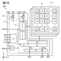
- FIG. 1A and 1B are diagrams showing an example of a storage device.
- FIG. 2A is a diagram showing a circuit configuration example of a memory cell.
- FIG. 2B is a graph showing the amount of polarization.
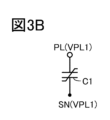
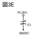
- 3A, 3B, 3C, 3D, and 3E are diagrams showing operation examples of the memory cell.
- FIG. 4 is a diagram showing an operation example of a memory cell.
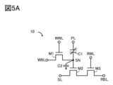
- 5A, 5B, and 5C are diagrams showing operation examples of the memory cell.
- 6A, 6B, and 6C are diagrams showing operation examples of the memory cell.
- FIG. 7 is a diagram showing an operation example of a memory cell.
- FIG. 8 is a cross-sectional view showing a configuration example of a semiconductor device.
- FIG. 8 is a cross-sectional view showing a configuration example of a semiconductor device.
- FIG. 9 is a cross-sectional view showing a configuration example of a semiconductor device.
- FIG. 10A is a cross-sectional view showing a configuration example of a semiconductor device.
- FIG. 10B is a cross-sectional view showing a configuration example of a transistor.
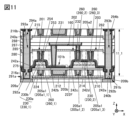
- FIG. 11 is a cross-sectional view showing a configuration example of a semiconductor device.
- FIG. 12 is a cross-sectional view showing a configuration example of a semiconductor device.
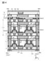
- FIG. 13 is a diagram showing a configuration example of a semiconductor device.
- FIG. 14 is a diagram showing a configuration example of a semiconductor device.
- FIG. 15 is a cross-sectional view showing a configuration example of a semiconductor device.
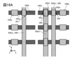
- 16A and 16B are plan views showing configuration examples of semiconductor devices.
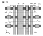
- 17A and 17B are plan views showing configuration examples of the semiconductor device.
- 18A and 18B are diagrams showing an example of a semiconductor device.
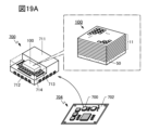
- 19A and 19B are diagrams showing an example of an electronic component.
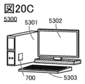
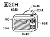
- 20A to 20J are diagrams illustrating examples of electronic devices.
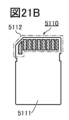
- 21A to 21E are diagrams illustrating examples of electronic devices.
- 22A to 22C are diagrams illustrating examples of electronic devices.
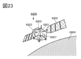
- FIG. 23 is a diagram showing an example of space equipment.
- the ordinal numbers “first” and “second” are used for convenience, and limit the number of constituent elements or the order of constituent elements (for example, the order of steps or the order of stacking). not something to do. Also, the ordinal number given to an element in one place in this specification may not match the ordinal number given to that element elsewhere in the specification or in the claims.
- film and “layer” can be interchanged depending on the case or circumstances.
- conductive layer can be changed to the term “conductive film.”
- insulating film can be changed to the term “insulating layer”.
- FIG. 1A shows a perspective schematic view of a storage device of one embodiment of the present invention.
- FIG. 1B shows a block diagram of a storage device of one embodiment of the present invention.
- the memory device 100 shown in FIGS. 1A and 1B has a drive circuit layer 50 and n memory layers 11 .
- the memory layers 11 each have a memory cell array 15 .
- a memory cell array 15 has a plurality of memory cells 10 .
- the n-layer memory layer 11 is provided on the drive circuit layer 50 .
- the area occupied by the memory device 100 can be reduced. Also, the storage capacity per unit area can be increased.
- the first memory layer 11 is indicated as a memory layer 11_1, the second memory layer 11 is indicated as a memory layer 11_2, and the third memory layer 11 is indicated as a memory layer 11_3.
- the k-th layer (k is an integer of 1 or more and n or less) is indicated as a memory layer 11_k
- the n-th layer 11 is indicated as a memory layer 11_n.
- the term "storage layer 11" is simply used. sometimes.
- the drive circuit layer 50 has a PSW 22 (power switch), a PSW 23 and a peripheral circuit 31 .
- the peripheral circuit 31 has a peripheral circuit 41 , a control circuit 32 and a voltage generation circuit 33 .
- each circuit, each signal, and each voltage can be omitted as appropriate. Alternatively, other circuits or other signals may be added.
- Signal BW, signal CE, signal GW, signal CLK, signal WAKE, signal ADDR, signal WDA, signal PON1, and signal PON2 are input signals from the outside, and signal RDA is an output signal to the outside.
- Signal CLK is a clock signal.
- Signal BW, signal CE, and signal GW are control signals.
- Signal CE is a chip enable signal
- signal GW is a global write enable signal
- signal BW is a byte write enable signal.
- Signal ADDR is an address signal.
- the signal WDA is write data and the signal RDA is read data.
- a signal PON1 and a signal PON2 are power gating control signals. The signal PON1 and the signal PON2 may be generated by the control circuit 32.
- the control circuit 32 is a logic circuit having a function of controlling the overall operation of the storage device 100 .
- the control circuit logically operates the signal CE, the signal GW, and the signal BW to determine the operation mode (for example, write operation, read operation) of the memory device 100 .
- the control circuit 32 generates a control signal for the peripheral circuit 41 so that this operation mode is executed.
- the voltage generation circuit 33 has a function of generating a negative voltage.
- the signal WAKE has a function of controlling the input of the signal CLK to the voltage generation circuit 33 . For example, when an H level signal is applied to signal WAKE, signal CLK is input to voltage generation circuit 33, and voltage generation circuit 33 generates a negative voltage.
- the peripheral circuit 41 is a circuit for writing data to and reading data from the memory cell 10 .
- the peripheral circuit 41 has a row decoder 42 , a column decoder 44 , a row driver 43 , a column driver 45 , an input circuit 47 , an output circuit 48 and a sense amplifier 46 .
- Row decoder 42 and column decoder 44 have the function of decoding signal ADDR.
- Row decoder 42 is a circuit for specifying a row to be accessed
- column decoder 44 is a circuit for specifying a column to be accessed.
- the row driver 43 has a function of selecting the wiring WWL (write word line) or the wiring RWL (read word line) specified by the row decoder 42 .
- the column driver 45 has a function of writing data to the memory cells 10, a function of reading data from the memory cells 10, a function of holding the read data, and the like.
- the column driver 45 has a function of selecting the wiring WBL (write bit line) and the wiring RBL (read bit line) specified by the column decoder 44 .
- Input circuit 47 has a function of holding signal WDA. Data held by the input circuit 47 is output to the column driver 45 . Output data of the input circuit 47 is data (Din) to be written to the memory cell 10 . Data (Dout) read from the memory cells 10 by the column driver 45 is output to the output circuit 48 .
- the output circuit 48 has a function of holding Dout. Also, the output circuit 48 has a function of outputting Dout to the outside of the storage device 100 . Data output from the output circuit 48 is the signal RDA.
- PSW 22 has a function of controlling the supply of VDD to peripheral circuit 31 .
- PSW 23 has the function of controlling the supply of VHM to row driver 43 .
- the high power supply voltage of the memory device 100 is VDD
- the low power supply voltage is GND (ground potential).
- VHM is a high power supply voltage used to drive word lines to a high level and is higher than VDD.
- the signal PON1 controls ON/OFF of the PSW22, and the signal PON2 controls ON/OFF of the PSW23.
- the number of power supply domains to which VDD is supplied is set to one, but may be set to a plurality. In this case, a power switch may be provided for each power domain.
- FIG. 1B shows an example in which a memory cell array 15 has a plurality of memory cells 10 arranged in a matrix of p rows and q columns (p and q are integers of 2 or more).
- rows and columns extend in directions orthogonal to each other.
- the X direction is the “row” and the Y direction is the “column”, but the X direction may be the “column” and the Y direction the "row”.
- the memory cell 10 provided in the 1st row and the 1st column is indicated as memory cell 10[1,1] and the memory cell 10 provided in the pth row and qth column is indicated as memory cell 10[p,q]. showing.
- the memory cell 10 provided in the i-th row and the j-th column (i is an integer of 1 to p and j is an integer of 1 to q) is denoted as memory cell 10[i,j].
- FIG. 2A shows a circuit configuration example of a memory cell.
- the memory cell 10 has a transistor M1, a transistor M2, a transistor M3, and a capacitor C1.
- a memory cell including three transistors and one capacitor is also called a 3Tr1C memory cell. Therefore, the memory cell 10 described in this embodiment is a 3Tr1C memory cell.
- the gate of the transistor M1 is electrically connected to the wiring WWL[j], and one of the source and the drain is electrically connected to the wiring WBL[i,s].
- the wiring WBL[i,s] is electrically connected to one of the source and drain of the transistor M1 included in the memory cell 10[i,j] of the other stacked memory layer 11 .
- FIG. 2A shows a configuration example in which the wiring WWL[j] has a function of applying the gate potential of the transistor M1.
- Capacitor C1 has a pair of electrodes. One electrode of the capacitor C1 is electrically connected to the wiring PL[j], and the other electrode is electrically connected to the other of the source and the drain of the transistor M1.
- FIG. 2A shows a configuration example in which the wiring PL[j] has a function of applying a potential to one electrode of the capacitor C1.
- the gate of the transistor M2 is electrically connected to the other electrode of the capacitor C1
- one of the source and the drain is electrically connected to one of the source and the drain of the transistor M3, and the other of the source and the drain is connected to the wiring SL[ i, s].
- the wiring SL[i,s] is electrically connected to the other of the source and the drain of the transistor M2 included in the memory cell 10[i,j] of the other stacked memory layer 11 .
- the gate of the transistor M3 is electrically connected to the wiring RWL[j], and the other of the source and the drain is electrically connected to the wiring RBL[i,s].
- the wiring RBL[i,s] is electrically connected to the other of the source and drain of the transistor M3 included in the memory cell 10[i,j] of the other stacked memory layer 11 .
- the other electrode of the capacitor C, the other of the source or drain of the transistor M1, and the gate of the transistor M2 are electrically connected to each other, and a region always having the same potential is referred to as a “node SN”. call.
- the gate of the transistor M1 is electrically connected to the wiring WWL[j+1], and one of the source and the drain is electrically connected to the wiring WBL[i, s+1].
- the wiring WBL[i, s+1] is electrically connected to either the source or the drain of the transistor M1 included in the memory cell 10[i, j+1] of the other stacked memory layer 11 .
- FIG. 2A shows a configuration example in which the wiring WWL[j+1] has a function of applying the gate potential of the transistor M1.
- One electrode of the capacitor C1 is electrically connected to the wiring PL[j+1], and the other electrode is electrically connected to the other of the source and the drain of the transistor M1. Note that, for example, FIG.
- the wiring PL[j+1] has a function of applying a potential to one electrode of the capacitor C1.
- the gate of the transistor M2 is electrically connected to the other electrode of the capacitor C1
- one of the source and the drain is electrically connected to one of the source and the drain of the transistor M3
- the other of the source and the drain is connected to the wiring SL[ i, s+1].
- the wiring SL[i, s+1] is electrically connected to the other of the source and the drain of the transistor M2 included in the memory cell 10[i, j+1] of the other stacked memory layer 11 .
- the gate of the transistor M3 is electrically connected to the wiring RWL[j+1], and the other of the source and the drain is electrically connected to the wiring RBL[i,s].
- the wiring RBL[i,s] is electrically connected to the other of the source and the drain of the transistor M3 included in the memory cell 10[i,j+1] of the other stacked memory layer 11 .
- the wiring RBL[i,s] corresponds to the other of the source or drain of the transistor M3 included in the memory cell 10[i,j] and the other of the source or drain of the transistor M3 included in the memory cell 10[i,j+1]. is electrically connected to Therefore, the wiring RBL[i,s] functions as a wiring for transmitting signals to the memory cells 10 located in adjacent columns.
- the wiring RBL[i,s] functions as a wiring that transmits a signal to the memory cell 10[i,j] and the memory cell 10[i,j+1].
- the wiring WBL[i,s] supplies signals to the memory cells 10 located in adjacent columns, for example, the memory cells 10[i,j ⁇ 1] and 10[i,j].
- the wiring WBL[i,s+1] transmits signals to the memory cells 10 located in adjacent columns, for example, the memory cells 10[i,j+1] and 10[i,j+2]. functions as a wire to transmit the
- the wiring SL[i,s] supplies signals to the memory cells 10 located in adjacent columns, for example, the memory cells 10[i,j ⁇ 1] and 10[i,j].
- the wiring SL[i, s+1] transmits a signal to the memory cells 10 located in adjacent columns, for example, the memory cells 10 [i, j+1] and 10 [i, j+2]. functions as a wire to transmit the
- a region in which the other electrode of the capacitor C1, the other of the source or drain of the transistor M1, and the gate of the transistor M2 are electrically connected to each other and always at the same potential is called a node SN. .
- transistors each having a back gate may be used as the transistor M1, the transistor M2, and the transistor M3.
- the gate and the back gate are arranged so as to sandwich the semiconductor channel forming region between the gate and the back gate.
- the gate and back gate are made of conductors.
- a back gate can function like a gate. Further, by changing the potential of the back gate, the threshold voltage of the transistor can be changed.
- the potential of the back gate may be the same potential as that of the gate, the ground potential, or an arbitrary potential.
- each of the transistor M1, the transistor M2, and the transistor M3 does not have to have a back gate.
- the gate and back gate are made of conductors, they also have a function of preventing an electric field generated outside the transistor from acting on the semiconductor in which the channel is formed (particularly, an electrostatic shielding function against static electricity). That is, it is possible to suppress fluctuations in the electrical characteristics of the transistor due to the influence of an external electric field such as static electricity.
- the amount of change in the threshold voltage of the transistor before and after a BT (Bias Temperature) test can be reduced by providing the back gate.
- the transistor M1 By using a transistor having a back gate as the transistor M1, the influence of an external electric field is reduced and the transistor M1 can be stably kept off. Therefore, the data written to the node SN can be held stably.
- the back gate By providing the back gate, the operation of the memory cell 10 is stabilized, and the reliability of the memory device including the memory cell 10 can be improved.
- the transistor M3 by using a transistor having a back gate as the transistor M3, the influence of an external electric field is reduced, and the transistor M3 can be stably kept off. Therefore, leakage current between the wiring RBL and the wiring SL is reduced, and power consumption of the memory device including the memory cell 10 can be reduced.
- a semiconductor device of one embodiment of the present invention includes a transistor including an oxide semiconductor, which is a kind of metal oxide, in a semiconductor layer in which a channel is formed (also referred to as an “OS transistor”).
- An OS transistor has a higher withstand voltage between a source and a drain than a transistor using silicon for a semiconductor layer in which a channel is formed (also referred to as a Si transistor).
- the memory cell 10 has sufficient resistance to the inversion polarization voltage of the ferroelectric layer, and the rewrite resistance of the memory cell 10 can be improved.
- the OS transistor since the OS transistor has high frequency characteristics, the semiconductor device can read and write data at high speed.
- OS transistors are preferably used as the transistor M1, the transistor M2, and the transistor M3.
- An oxide semiconductor has a bandgap of 2 eV or more, and thus has a significantly low off-state current. Therefore, power consumption of the memory cell 10 can be reduced. Therefore, the power consumption of the memory device 100 including the memory cells 10 can be reduced.
- a semiconductor layer in which channels of the transistors M1, M2, and M3 are formed a single crystal semiconductor, a polycrystalline semiconductor, a microcrystalline semiconductor, an amorphous semiconductor, or the like may be used alone or in combination.
- Silicon or germanium for example, can be used as the semiconductor material.
- Compound semiconductors such as silicon germanium, silicon carbide, gallium arsenide, oxide semiconductors, or nitride semiconductors may also be used.
- a memory cell including an OS transistor can also be called an "OS memory.” Further, the memory device 100 including the memory cell can also be called an "OS memory”.
- the OS transistor operates stably even in a high-temperature environment and has little characteristic variation.
- the off current hardly increases even in a high temperature environment.
- the off current hardly increases even under an environmental temperature of room temperature or higher and 200° C. or lower.
- the on-current is less likely to decrease even in a high-temperature environment. Therefore, the OS memory can operate stably even in a high-temperature environment and obtain high reliability.
- OS transistors have better electrical characteristics than Si transistors in high-temperature environments. Specifically, even at a high temperature of 100° C. to 200° C., preferably 125° C. to 150° C., the ratio of the on-current to the off-current is large, so that good switching operation can be performed.
- a ferroelectric is preferably used as the dielectric of the capacitor C1.
- the storage device of one embodiment of the present invention can retain data for a long time. Accordingly, the frequency of refreshing (rewriting data to cells) can be reduced, so that power consumption of the memory device of one embodiment of the present invention can be reduced.
- the capacitor provided with the ferroelectric layer between the first electrode and the second electrode retains data for a long time without adopting a structure for increasing the capacitance, such as a trench structure. be able to. As a result, a storage device having an easy-to-manufacture structure can be obtained.
- Capacitors with ferroelectric layers are sometimes called ferroelectric capacitors.
- a capacitor with a ferroelectric layer when a voltage (electric field or electric field) is applied between two electrodes sandwiching the ferroelectric layer, the ferroelectric layer changes depending on the direction and amount of voltage application. The direction of polarization and the amount of polarization change. Signals (data) are stored (written) between two electrodes sandwiching the ferroelectric layer using the change in the polarization state of the ferroelectric layer. After data is stored (written) into the capacitor, polarization remains in the ferroelectric layer (residual polarization) even when the voltage between the two electrodes sandwiching the ferroelectric layer is reduced to zero. In order to rewrite the polarization, a voltage for reversing the polarization (polarization reversal voltage) is applied.
- FIG. 2B is a graph showing the magnitude of polarization (polarization amount) according to the electric field applied to the ferroelectric layer.
- the horizontal axis indicates the electric field E applied to the ferroelectric layer.
- the vertical axis indicates the amount of polarization P of the ferroelectric layer.
- the polarization of the ferroelectric layer increases.
- the electric field applied to the ferroelectric layer is lowered after the electric field EH is applied to the ferroelectric layer, positive charges are biased toward one electrode side of the capacitor, and negative charges are biased toward the other electrode side of the capacitor. Because of the bias, positive polarization remains when the electric field becomes zero.
- the electric field applied to the ferroelectric layer is lowered, the polarization of the ferroelectric layer becomes smaller.
- the electric field applied to the ferroelectric layer is increased after the electric field EL is applied to the ferroelectric layer, the positive charges are biased toward the other electrode side of the capacitor C1, and the negative charges are biased toward the one electrode side of the capacitor.
- a voltage for applying the electric field EH and the electric field EL to the ferroelectric layer can be called a polarization reversal voltage.
- Data can be written to the memory cell 10 by applying a polarization inversion voltage to the capacitor C1.
- the electric field E R can be, for example, an electric field (coercive electric field) in which the polarization becomes zero.
- the voltage for applying the electric field E R to the ferroelectric layer can be said to be the voltage that does not cause polarization reversal.
- a voltage that does not cause polarization inversion to the capacitor C1 it is possible to read out data from the memory cell 10 by amplifying the change in potential corresponding to the amount of change in polarization (P H , P L ).
- a negative electric field is shown as the electric field ER , but it may be a positive electric field.
- the memory device including the memory cell 10 is excellent in reliability of read data.
- the memory device including the memory cell 10 can achieve low power consumption.
- the area of the capacitor can be reduced as compared with a capacitor having a paraelectric.
- Materials that can be used for the ferroelectric layer and can have ferroelectricity include hafnium oxide, zirconium oxide, HfZrO x (X is a real number greater than 0), hafnium oxide and element J1 (here, The element J1 is a material to which zirconium (Zr), silicon (Si), aluminum (Al), gadolinium (Gd), yttrium (Y), lanthanum (La), strontium (Sr), etc.) is added, and an element to zirconium oxide.
- element J2 here is hafnium (Hf), silicon (Si), aluminum (Al), gadolinium (Gd), yttrium (Y), lanthanum (La), strontium (Sr), etc.) added material , and so on.
- the atomic ratio of the hafnium atoms and the element J1 can be appropriately set.
- the ratio of hafnium atoms and zirconium atoms may be 1:1 or in the vicinity thereof.
- the ratio of the number of atoms of the zirconium atoms and the element J2 can be set as appropriate.
- Materials that can have ferroelectricity include PbTiO x , barium strontium titanate (BST), strontium titanate, lead zirconate titanate (PZT), strontium bismuthate tantalate (SBT), and bismuth ferrite (BFO). , barium titanate, and other piezoelectric ceramics having a perovskite structure may also be used.
- a material that can have ferroelectricity for example, a plurality of materials selected from the materials listed above, or a laminated structure composed of a plurality of materials selected from the materials listed above can be used. can.
- hafnium oxide, zirconium oxide, HfZrO x , and materials obtained by adding the element J1 to hafnium oxide may change their crystal structures (characteristics) depending not only on film formation conditions but also on various processes.
- materials exhibiting ferroelectricity are called ferroelectrics, but also materials capable of having ferroelectricity or materials having ferroelectricity are called.
- Materials that can have ferroelectricity include scandium aluminum nitride (Al1 - aScaNb (a is a real number greater than 0 and less than 0.5, and b is 1 or a value in the vicinity thereof ). hereinafter simply referred to as AlScN)), Al--Ga--Sc nitrides, Ga--Sc nitrides, and the like can be used.
- AlScN scandium aluminum nitride
- Al-Ga--Sc nitrides Al--Ga--Sc nitrides
- Ga--Sc nitrides and the like
- a metal nitride containing an element M1, an element M2, and nitrogen can be used as a material that can have ferroelectricity.
- the element M1 is one or more selected from aluminum (Al), gallium (Ga), indium (In), and the like.
- Element M2 includes boron (B), scandium (Sc), yttrium (Y), lanthanides (lanthanum (La), cerium (Ce), praseodymium (Pr), neodymium (Nd), promethium (Pm), samarium ( Sm), europium (Eu), gadolinium (Gd), terbium (Tb), dysprosium (Dy), holmium (Ho), erbium (Er), thulium (Tm), ytterbium (Yb), and lutetium (Lu)), Actinide (15 elements from actinium (Ac) to lawrencium (Lr)), titanium (Ti), zirconium (Zr), hafnium (Hf), vanadium (V), niobium (Nb), tantalum (Ta), chromium ( Cr) and the like.
- Actinide (15 elements from actinium (Ac) to lawrencium (Lr)),
- the ratio between the number of atoms of the element M1 and the number of atoms of the element M2 can be set as appropriate.
- a metal oxide containing the element M1 and nitrogen may have ferroelectricity even if it does not contain the element M2.
- a material that can have ferroelectricity a material obtained by adding an element M3 to the metal nitride can be used.
- Element M3 is one or more selected from magnesium (Mg), calcium (Ca), strontium (Sr), zinc (Zn), cadmium (Cd), and the like.
- the ratio of the number of atoms of the element M1, the number of atoms of the element M2, and the number of atoms of the element M3 can be set as appropriate.
- the metal nitride contains at least a group 13 element and nitrogen, which is a group 15 element
- the metal nitride is used as a group 13-15 ferroelectric and a strong material of a group 13 nitride. They are sometimes called dielectrics.
- perovskite-type oxynitrides such as SrTaO 2 N and BaTaO 2 N, GaFeO 3 with a ⁇ -alumina structure, and the like can be used.
- the material that can have ferroelectricity can be, for example, a mixture or a compound composed of a plurality of materials selected from the materials listed above.
- the material that can have ferroelectricity can have a laminated structure composed of a plurality of materials selected from the materials listed above.
- the materials listed above may also be called materials capable of having ferroelectricity or materials having ferroelectricity.
- a hafnium oxide layer or a layer containing hafnium oxide and zirconium oxide is preferable as a ferroelectric layer because it can have ferroelectricity even if it is processed into a thin film of several nm.
- a ferroelectric layer that can be thinned a memory device combined with a miniaturized transistor can be obtained.
- HfZrO X when used as a material capable of having ferroelectricity, it is preferable to use an atomic layer deposition (ALD) method, particularly a thermal ALD method, for film formation. Further, in the case of forming a film of a material that can have ferroelectricity by using the thermal ALD method, it is preferable to use a material that does not contain hydrocarbon (hydrocarbon, also called HC) as a precursor. When one or both of hydrogen and carbon are contained in the material that can have ferroelectricity, crystallization of the material that can have ferroelectricity may be inhibited.
- ALD atomic layer deposition
- hydrocarbon-free precursors include chlorine-based materials.
- HfZrO x hafnium oxide and zirconium oxide
- one or both of HfCl 4 and ZrCl 4 may be used as the precursor.
- the ALD method is a film forming method in which a precursor and a reactant (for example, an oxidizing agent) are alternately introduced, and since the film thickness can be adjusted by the number of times this cycle is repeated, precise film thickness adjustment is possible. be.
- heat treatment for example, an RTA (Rapid Thermal Anneal) device, a resistance heating furnace, or a microwave heating device can be used.
- RTA Rapid Thermal Anneal
- a resistance heating furnace for example, a resistance heating furnace, or a microwave heating device.
- a film having particularly excellent ferroelectricity may be obtained, which is preferable.
- impurities in the film here at least one of hydrogen, hydrocarbon, and carbon, are thoroughly eliminated to obtain a highly pure intrinsic film. It is possible to form a film having good ferroelectricity. Note that a highly purified intrinsic ferroelectric film and a highly purified intrinsic oxide semiconductor described in an embodiment described later have very high compatibility in manufacturing processes. Therefore, a method for manufacturing a memory device with high productivity can be provided.
- HfZrO 2 X when used as a material capable of having ferroelectricity, it is preferable to alternately deposit hafnium oxide and zirconium oxide so as to have a composition of 1:1 using thermal ALD.
- H 2 O or O 3 can be used as an oxidizing agent.
- the oxidizing agent for the thermal ALD method is not limited to this.
- the oxidizing agent for the thermal ALD method may include any one or more selected from O2 , O3 , N2O , NO2 , H2O , and H2O2 .
- the crystal structure of the material that can have ferroelectricity is not particularly limited.
- the crystal structure of a material that can have ferroelectricity may be one or more selected from a cubic system, a tetragonal system, a rectangular system, and a monoclinic system.
- a material that can have ferroelectricity it is preferable to have a cubic crystal structure because ferroelectricity is exhibited.
- a composite structure having an amorphous structure and a crystalline structure may be used as a material capable of having ferroelectricity.
- the wiring WBL is a wiring to which a signal (data signal) corresponding to data written to the memory cell 10 is supplied.
- the wiring WBL may also be called a write bit line.
- the wiring WBL can be a wiring shared with another wiring, for example, the wiring RBL.
- the wiring WWL is a wiring supplied with a signal (selection signal) for writing data to the memory cell 10 .
- the wiring WWL may also be called a write word line.
- the wiring PL is supplied with a signal (control signal) for writing data to the memory cell 10 and a signal (control signal) for reading data from the memory cell 10 .
- the wiring PL has a function of controlling the polarization state of the ferroelectric layer of the capacitor C1, and is sometimes referred to as a polarization control line.
- the wiring SL is a wiring supplied with a constant potential for reading data from the memory cell 10 .
- the wiring SL has a function of allowing current to flow between it and the wiring RBL according to data stored in the memory cell 10, and is sometimes called a source line.
- the wiring RBL is a wiring supplied with a signal according to data read from the memory cell 10 .
- the wiring RBL may also be called a read bit line.
- the wiring RBL can be a wiring shared with another wiring, for example, the wiring WBL.
- each transistor is described as an n-channel transistor.
- the transistor M1 can be turned on by setting the wiring WWL to a high potential (also referred to as an H-level potential or H-level).
- the wiring WWL is set to a low potential (also referred to as an L-level potential or an L-level)
- the transistor M1 can be turned off. The same is true for the transistor M3.
- Data is written to the memory cell 10 according to the direction of the electric field applied to the ferroelectric layer of the capacitor C1 given by the potential of the node SN and the potential of the wiring PL.
- the data signal to be written applies a polarization inversion voltage to the capacitor C1.
- the ferroelectric layer of the capacitor C1 can assume different polarization states depending on the data signal.
- the capacitance value of the capacitor C1 can be varied according to this polarization state. This polarization state and the difference in the capacitance value of the capacitor C1 are maintained even when the electric field to the capacitor C1 is zero.
- Data is read from the memory cell 10 using capacitive coupling at the capacitor C1 when the potential of the wiring PL is changed.
- the potential of the wiring PL is set so that the voltage applied to the capacitor C1 does not reverse the polarization of the ferroelectric layer.
- capacitive coupling occurs in the capacitor C1. Therefore, the potential of the node SN changes according to a change in the potential of the wiring PL.
- a change in the potential of the node SN differs depending on the state of the capacitance value of the capacitor C1. Therefore, the potential of the gate of the transistor M2 can be varied according to the stored data.
- the different potentials of the gates of the transistors result in different amounts of current flowing between the source and drain of the transistor M2. Data can be read from the memory cell 10 based on the difference in current amount.
- FIG. 3A is a timing chart for explaining the data write operation in the memory cell 10 shown in FIG. 2A.
- FIG. 3A shows signals or potentials of the wiring WWL, the wiring WBL, the wiring PL, the node SN, the wiring RBL, the wiring RWL, and the wiring SL in the memory cell 10 .
- FIG. 3A also shows “data1” and “data0” as data to be written in the memory cell 10 .
- “data1” is shown as an H level signal
- “data0” is shown as an L level signal.
- the wiring WWL is set to H level.
- a signal corresponding to data data1 or data0 to be written to the memory cell 10 is applied to the wiring WBL, and a potential corresponding to the signal is applied to the node SN.
- the wiring PL is set to H level.
- the wiring RBL, the wiring RWL, and the wiring SL are set to L level.
- An H-level signal applied to the wiring WBL, the wiring PL, and the node SN is indicated as a potential VPL1, and an L-level signal is indicated as a potential 0V.
- the potential VPL1 is a potential at which the potential VPL1 is applied to one electrode of the capacitor C1 and a potential of 0 V is applied to the other electrode, thereby applying a reverse polarization voltage to the ferroelectric layer of the capacitor C1.
- Potential VPL1 is preferably 2.5 V or higher.
- the transistors M1 to M3 are preferably transistors with high resistance (withstand voltage) to high voltage.
- the rewrite resistance of the memory cell 10 can be improved by forming the transistors M1 to M3 with OS transistors having higher withstand voltage characteristics than Si transistors.
- the potential shown in FIG. 3B is applied to the electrode of the capacitor C1.
- the electrodes at both ends of the capacitor C1 are both at the same potential as the potential VPL1, so that no voltage exceeding the inversion polarization voltage is applied and no electric field is generated on the ferroelectric layer.
- the potential shown in FIG. 3C is applied to the electrode of the capacitor C1. As shown in FIG.
- a voltage VPL1 which is an inversion polarization voltage, is applied to the electrodes of the capacitor C1, and an electric field EL is generated in the ferroelectric layer. Therefore, the polarization state corresponding to data0 is written into the capacitor C1.
- the wiring WWL is set to the H level following the period P11.
- a signal corresponding to data data1 or data0 to be written to the memory cell 10 is applied to the wiring WBL in the period P11, and a potential corresponding to the signal is applied to the node SN.
- the wiring PL is set to L level.
- the wiring RBL, the wiring RWL, and the wiring SL are set to L level.
- the potential shown in FIG. 3D is applied to the electrode of the capacitor C1.
- an electric field opposite to the period P11 is applied to the pair of electrodes of the capacitor C1
- a voltage VPL1 that is an inversion polarization voltage is applied to the electrodes of the capacitor C1
- the electric field is applied to the ferroelectric layer. EH is produced. Therefore, the polarization state corresponding to data1 is written into the capacitor C1.
- the electrodes of the capacitor C1 are both at the same potential as the potential 0 V, as shown in FIG. 3E. It is not applied and does not create an electric field on the ferroelectric layer.
- FIG. 4 is a timing chart for explaining the data read operation in the memory cell 10 shown in FIG.
- FIG. 4 shows signals or potentials of the wiring WWL, the wiring WBL, the wiring PL, the node SN, the wiring RBL, the wiring RWL, and the wiring SL in the memory cell 10 .
- FIG. 4 also shows “data1” and “data0” as data read from the memory cell 10 .
- "data1" and “data0” correspond to the data stored as the polarization state of the ferroelectric layer of the capacitor C1 in the data write operation.
- the wiring WWL is at L level. Node SN is in an electrically floating state.
- the wiring PL is set to the potential VPL2.
- the wiring WBL, the wiring RWL, and the wiring SL are set to L level.
- the wiring RBL is precharged to a potential that varies depending on the currents flowing through the transistors M2 and M3 in a period before the period P21. For example, it is precharged to a potential lower than the potential VPL1.
- the node SN in the memory cell 10 has a capacitance C2 that is a parasitic capacitance such as the gate capacitance of the transistor M2.
- C2 a parasitic capacitance such as the gate capacitance of the transistor M2.
- the amount of change ⁇ V SN in the potential V SN of the node SN is determined by the capacitance value C FE of the capacitor C1, the capacitance value C S of the capacitor C2, and the amount of change ⁇ VPL2 in the voltage VPL2 corresponding to the voltage of the capacitor C1. can be represented.
- the capacitance value CFE of the capacitor C1 is determined by the polarization state of the ferroelectric layer of the capacitor C1. This polarization state differs according to the written data "data1" or “data0". Therefore, the potential VSN of the node SN can be changed depending on the written data "data1" or "data0".
- the capacitance value CS of the parasitic capacitance (capacitor C2) of the node SN is smaller than the capacitance value CFE of the capacitance C1 having the ferroelectric layer.
- a potential difference due to a difference in capacitance value according to the polarization state of the capacitor C1 appears as Vdata0 or Vdata1 in the potential VSN of the node SN.
- the wiring RWL is set to H level. Conduction is established between the source and the drain of the transistor M3. A current corresponding to the potential of the node SN flows through the transistor M2.
- the potential of the node SN can take two states of potential Vdata0 and potential Vdata1 (>Vdata0) as illustrated in FIGS. 5B and 5C.
- a current Idata0 or Idata1 (>Idata0) according to the potential Vdata0 or Vdata1 flows through the transistor M2.
- the potential of the precharged wiring RBL changes due to the flow of the current Idata0 or Idata1.
- the potential of the wiring RBL after the change is determined according to the magnitude of the current (Idata0 or Idata1) flowing through the transistor M2.
- Whether the written data is “data1” or “data0” is determined by comparing the magnitude relationship between the potential of the wiring RBL after the change and the reference voltage VREF , and data is read from the memory cell 10 . can be done.
- the potential of the wiring RBL becomes higher than the reference voltage VREF . lower than the voltage V - - REF .
- the potential of the wiring RBL to be precharged is preferably lower than the potential VPL1. With this structure, fluctuation in the potential of the wiring RBL can be reduced. Therefore, even if a circuit including a transistor electrically connected to the wiring RBL is a miniaturized transistor such as a Si transistor and has a low withstand voltage, the circuit can be operated without problems.
- the operation of reading data from the memory cell 10 in FIG. 2A can be configured differently. For example, it may be operated as shown in the timing chart of FIG. 6A.
- the potential of the wiring SL is increased, and a current corresponding to the potential of the node SN is flowed while the wiring RBL is precharged to 0V. That is, as illustrated in FIGS. 6B and 6C, a current Idata0 or Idata1 (>Idata0) corresponding to the potential Vdata0 or Vdata1 flows through the transistor M2 from the wiring SL toward the wiring RBL.
- Data can be read from the memory cell 10 by comparing the magnitude relationship between the potential of the wiring RBL and the reference voltage VREF .
- the potential of the wiring RBL becomes lower than the reference voltage VREF . higher than the voltage V-- REF .
- the operation of reading data from the memory cell 10 of FIG. 2A can be performed in another operation method. For example, it may be operated as shown in the timing chart of FIG.
- FIG. 7 corresponds to the operation method in which the operation of setting the potential of the node SN is added to FIG.
- the potential of the wiring WBL is set to a desired potential VPRE_SN
- the potential of the wiring WWL is set to H level.
- the potential of the node SN becomes the potential VPRE_SN .
- the wiring WWL is set to L level, and the node SN is kept in an electrically floating state.
- the potential of the node SN which changes when the potential of the wiring PL is changed in the period P21, can be easily set to the current that the transistor M2 flows.
- One embodiment of the present invention relates to a semiconductor device in which a memory layer is provided over a substrate.
- the memory layer has a first transistor, a second transistor, a third transistor, and a capacitor, which can constitute a memory cell. Since a semiconductor device of one embodiment of the present invention includes memory cells, it has a function of storing data. Therefore, a semiconductor device of one embodiment of the present invention can be called a memory device.
- a plurality of memory layers having the above structure are stacked.
- a plurality of memory layers having the above structure are provided, for example, in a direction perpendicular to the substrate surface.
- the OS transistor a semiconductor layer in which a channel is formed can be formed by a thin film method such as a sputtering method.
- the OS transistor can be formed at a low temperature, for example, a temperature of 750° C. or lower. Therefore, a plurality of layers each including an OS transistor can be stacked.
- An OS transistor can be preferably used for a plurality of stacked memory layers.
- the OS transistor can be freely arranged by stacking it on a circuit using a Si transistor or the like, integration can be easily performed.
- silicon for example, amorphous silicon (sometimes referred to as hydrogenated amorphous silicon), microcrystalline silicon, polycrystalline silicon, monocrystalline silicon, or the like can be used.
- an OS transistor can be manufactured using a manufacturing apparatus similar to that of a Si transistor, it can be manufactured at low cost.
- a gain cell type memory cell requires at least two transistors per memory cell, and it is difficult to increase the number of memory cells that can be arranged per unit area. , a plurality of memory cell arrays 15 can be stacked. That is, the amount of data that can be stored per unit area can be increased.
- the write bit line and the read bit line can be provided, for example, in a direction perpendicular to the substrate surface.
- n is an integer of 2 or more
- an opening is provided to penetrate the n storage layers, and a conductor is formed inside the opening.
- write bit lines, and read bit lines can be formed.
- a conductor having regions functioning as write bit lines is provided so as to have regions in contact with the top surface and side surfaces of the first conductor.
- FIG. 8 is a cross-sectional view illustrating a structural example of a semiconductor device of one embodiment of the present invention.
- the semiconductor device shown in FIG. 8 can be applied to the circuit configuration of the memory cell shown in the above embodiment.
- insulator 8 includes an insulator 210 over a substrate (not shown), conductors 209a and 209b embedded in the insulator 210, an insulator 212 over the insulator 210, and an insulator
- the insulator 214 on the insulator 212, the n-layer storage layer 11 on the insulator 214, and the n-layer extending in the Z direction are provided so as to be conductive.
- the components included in the semiconductor device of this embodiment may each have a single-layer structure or a laminated structure.
- the conductor 209 may be used when describing items common to the conductor 209a and the conductor 209b.
- a memory cell array having a plurality of memory cells is provided in each of the memory layers 11_1 to 11_n.
- a memory cell includes a transistor 201 , a transistor 202 , a transistor 203 , and a capacitor 101 .
- the conductor 240a has a region that functions as a write bit line
- the conductor 240b has a region that functions as a read bit line.
- the transistor 201, the transistor 202, the transistor 203, and the capacitor 101 can correspond to the transistor M1, the transistor M2, the transistor M3, and the capacitor C1 included in the memory cell 10 described in the above embodiment, respectively.
- the conductor 240a and the conductor 240b can correspond to the wiring WBL and the wiring RBL, respectively.
- the direction parallel to the channel length direction of the illustrated transistor is defined as the X direction
- the direction parallel to the channel width direction of the illustrated transistor is defined as the Y direction.
- the X and Y directions may be directions perpendicular to each other.
- the direction perpendicular to both the X direction and the Y direction ie, the direction perpendicular to the XY plane, is defined as the Z direction.
- the X direction and Y direction can be, for example, parallel to the substrate surface, and the Z direction can be perpendicular to the substrate surface.
- the conductors 209a and 209b function as parts of circuit elements such as switches, transistors, capacitors, inductors, resistors, and diodes, wirings, electrodes, or terminals.
- FIG. 8 shows a memory layer 11_1 as the lowest layer, a memory layer 11_2 above the memory layer 11_1, and a memory layer 11_n as the top layer among the n memory layers.
- the conductors 209 a and 209 b are electrically connected to a driver circuit for driving memory cells provided in the memory layer 11 .
- the driver circuit is provided below the conductors 209a and 209b.
- the transistors 201 , 202 , and 203 are provided over the insulator 214 . Here, the transistors 202 and 203 share some layers.
- a capacitor 101 is provided above the transistors 201 to 203 .
- FIG. 9 shows an example having connection electrodes 240c and 240d instead of the conductors 240a and 240b.
- the memory layer 11 is electrically connected to a conductor 233a electrically connected to a conductor 242a (detailed in FIG. 10) included in the transistor 201 and a conductor 242e (detailed in FIG. 10) included in the transistor 203. and a conductor 233b connected to the .
- the conductor 233a and the conductor 233b included in the memory layer 11 — k which is the k-th memory layer 11 (k is an integer of 1 or more and n or less), are represented as a conductor 233a[k] and a conductor 233b[k], respectively. .
- connection electrode 240c has conductors 233a[1] to 233a[n] (not shown), which are electrically connected.
- connection electrode 240d includes conductors 233b[1] to 233b[n] (not shown), which are electrically connected.
- FIG. 10A is a cross-sectional view showing a structural example of the conductor 209a, the conductor 209b, the insulator 210, the insulator 212, the insulator 214, and the memory layer 11_1.
- an insulator 282 is provided over the transistors 201 to 203 and an insulator 285 is provided over the insulator 282 .
- the transistor 201, the transistor 202, and the transistor 203 include a conductor 205a1 over the insulator 214, an insulator 222 over the conductor 205a1, an insulator 224 over the insulator 222, and a metal oxide over the insulator 224, respectively.
- 230 metal oxide 230a and metal oxide 230b
- the transistor 201 includes conductors 242a and 242b as the conductors 242
- the transistor 202 includes conductors 242c and 242d as the conductors 242
- the transistor 203 includes the conductors 242a and 242d.
- a conductor 242d and a conductor 242e are indicated as a conductor 205a1_1, a conductor 205a1_2, and a conductor 205a1_3, respectively.
- the conductors 260 included in the transistors 201, 202, and 203 are denoted as conductors 260_1, 260_2, and 260_3, respectively.
- the metal oxide 230 included in the transistor 201 is denoted by 230_1, and the metal oxide 230 shared between the transistors 202 and 202 is denoted by 230_2.
- the insulator 222 is sandwiched between the conductor 205 a 1 of the transistor 201 and the metal oxide 230 , is sandwiched between the conductor 205 a 1 of the transistor 202 and the metal oxide 230 , and is sandwiched between the conductor 205 a 1 of the transistor 202 and the metal oxide 230 .
- the conductor 205a1 preferably has a region in contact with the lower surface of the insulator 222. In the structure shown in FIG.
- An insulator 216a having an opening is provided over the insulator 214, and the conductor 205a1 is embedded in the opening.
- An insulator 222 is provided over the conductor 205a1 and the insulator 216a.
- An insulator 275 is provided over the conductors 242 a to 242 e , and an insulator 280 is provided over the insulator 275 .
- the insulator 253 , the insulator 254 , and the conductor 260 are embedded inside openings provided in the insulator 280 and the insulator 275 .
- An insulator 282 is provided over the insulator 280 and the conductor 260 .
- the conductor 205a1 can have a region in contact with the side surface of the insulator 216a.
- the insulator 253 may have a region contacting at least part of the side surfaces of the conductor 242 , the insulator 275 , and the insulator 280 .
- the metal oxide 230 has regions that function as channel formation regions of the transistor 201 , the transistor 202 , or the transistor 203 .
- a semiconductor such as single crystal silicon, polycrystalline silicon, or amorphous silicon may be used instead of the metal oxide 230.
- LTPS low temperature polysilicon
- : Low Temperature Poly Silicon may be used.
- the conductor 242 a has a region that functions as one of the source and drain electrodes of the transistor 201 .
- the conductor 242b has a region that functions as the other of the source and drain electrodes of the transistor 201 .
- Conductor 242 c has a region that functions as one of the source and drain electrodes of transistor 202 .
- the conductor 242 d has regions that function as the other of the source and drain electrodes of the transistor 202 and one of the source and drain electrodes of the transistor 203 .
- the conductor 242 e has a region that functions as the other of the source and drain electrodes of the transistor 203 .
- Conductor 260 has a region that functions as a first gate electrode of transistor 201 , transistor 202 , or transistor 203 .
- Insulators 253 and 254 have regions that function as first gate insulators of transistor 201, transistor 202, or transistor 203, respectively.
- the conductor 205 a 1 has a region functioning as a second gate electrode of the transistor 201 , the transistor 202 , or the transistor 203 .
- Insulator 222 includes a region that functions as a second gate insulator for transistor 201, a region that functions as a second gate insulator for transistor 202, a region that functions as a second gate insulator for transistor 203, have Insulator 224 has a region that functions as a second gate insulator for transistor 201 , transistor 202 , or transistor 203 .
- the first gate electrode can be called a front gate electrode or simply a gate electrode
- the second gate electrode can be called a back gate electrode.
- the first gate electrode may be called a back gate electrode
- the second gate electrode may be called a front gate electrode or simply a gate electrode.
- Transistors 202 and 203 are adjacent and share metal oxide 230 and conductor 242d, respectively, as previously described. Accordingly, two transistors (transistor 202 and transistor 203) can be formed in an area smaller than the area of two transistors (for example, the area of 1.5 transistors). Therefore, compared to the case where the transistor 202 and the transistor 203 do not share the metal oxide 230 and the conductor 242d, the transistors can be arranged at a higher density, and high integration of the semiconductor device can be achieved.
- a conductor 242 d is provided in a region between the conductor 260 of the transistor 202 and the conductor 260 of the transistor 203 . Therefore, an n-type region (low-resistance region) can be formed in a region of the metal oxide 230 which overlaps with the conductor 242d. In particular, an n-type region can be formed in the region of metal oxide 230b that overlaps conductor 242d. In addition, current can flow between the transistor 202 and the transistor 203 through the conductor 242d. Therefore, the resistance component between the transistor 202 and the transistor 203 can be significantly reduced compared to the configuration in which two Si transistors are connected in series.
- the conductor 242 d partially covers the side surface of the metal oxide 230 .
- the conductor 242d covers side surfaces of the metal oxide 230 in a cross section of the transistor 202 in the channel width direction including the conductor 242d.
- An insulator 285 is provided over the insulator 282 .
- the insulator 280, the insulator 282, and the insulator 285 are provided with openings reaching the conductor 242b, and the conductor 231 is embedded inside the openings.
- the insulators 282 and 285 are provided with openings reaching the conductor 260 of the transistor 202, and the conductor 232 is provided inside the openings.
- the capacitor 101 includes an insulator 285 , a conductor 231 , a conductor 161 over the conductor 232 , an insulator 163 over the conductor 161 , and a conductor 162 over the insulator 163 .
- the insulator 163 has a region sandwiched between the conductors 161 and 162 .
- the conductor 161 has a region that functions as one electrode (also referred to as a lower electrode) of the capacitor 101 .
- Insulator 163 has a region that functions as a dielectric for capacitor 101 .
- the conductor 162 has a region that functions as the other electrode (also referred to as an upper electrode) of the capacitor 101 .
- a capacitor 101 constitutes an MIM capacitor.
- the conductor 231 electrically connects the conductor 242 b and the conductor 161 .
- the conductor 232 electrically connects the conductor 260 included in the transistor 202 and the conductor 161 .
- the conductor 242b having a region functioning as the other of the source electrode and the drain electrode of the transistor 201 has a region functioning as the gate electrode of the transistor 202 with the conductors 231, 161, and 232 interposed therebetween. It is electrically connected to the conductor 260 provided.
- An insulator 287 is provided over the conductor 162 and the insulator 163 .
- An insulator 215 is provided over the insulator 287 .
- An insulator 216b having an opening is provided over the insulator 215, and the conductor 205a2 is embedded in the opening.
- the conductor 205a may be referred to as the conductor 205a when items common to the conductor 205a1 and the conductor 205a2 are described.
- the conductors 242 a , 242 b , 242 c , and 242 e extend beyond the metal oxide 230 functioning as a semiconductor layer and cover part of the top surface and side surfaces of the metal oxide 230 . Therefore, the conductors 242a, 242b, 242c, and 242e also function as wirings.
- a conductor 240a is provided having regions that function as write bit lines, such that it has regions that contact portions of the top, side, and bottom surfaces of conductor 242a.
- a conductor 240b having a region functioning as a read bit line is provided so as to have a region in contact with part of the top surface, side surfaces, and bottom surface of the conductor 242e.
- the conductor 242d can also function as a wiring. Other wires may also function as wires.
- the conductor 240a functioning as a write bit line has a region in contact with part of the top surface, the side surface, and the bottom surface of the conductor 242a, a separate electrode for connection is provided between the write bit line and the conductor 242a. no longer needed.
- the conductor 240b functioning as a read bit line has a region in contact with part of the upper surface, the side surface, and the lower surface of the conductor 242e, a separate electrode for connection is provided between the read bit line and the conductor 242e. no longer need to be set. Therefore, the area occupied by the memory cell array can be reduced. Also, the degree of integration of memory cells is improved, and the storage capacity can be increased.
- the conductor 240a has a region in contact with one or more, preferably two or more, top, side, and bottom surfaces of the conductor 242a, and the conductor 240b has one of the top, side, and bottom surfaces of the conductor 242e. It has a region that contacts more than one, more preferably two or more. Contact resistance between the conductor 240a and the conductor 242a can be reduced by bringing the conductor 240a into contact with multiple surfaces of the conductor 242a. Contact resistance between the conductors 242e can be reduced.
- the insulators 212 and 214 are provided with an opening 291a having a region overlapping with the conductor 209a and an opening 291b having a region overlapping with the conductor 209b.
- the insulator 222 is provided with an opening 292a having a region overlapping with the conductor 209a and the opening 291a and an opening 292b having a region overlapping with the conductor 209b and the opening 291b.
- the insulator 282 is provided with an opening 293a having a region overlapping with the conductor 209a, the opening 291a, and the opening 292a, and an opening 293b having a region overlapping with the conductor 209b, the opening 291b, and the opening 292b.
- the insulator 215 includes an opening 294a having a region overlapping with the conductor 209a, the opening 291a, the opening 292a, and the opening 293a, and an opening 294b having a region overlapping with the conductor 209b, the opening 291b, the opening 292b, and the opening 293b. is provided.
- a conductor 240a is provided inside the openings 291a to 294a, and a conductor 240a is provided inside the openings 291b to 294b. Note that the insulator 212 does not have to have the opening 291a.
- the side surfaces of the insulator 212 and the side surfaces of the insulator 214 are covered with the insulator 216a.
- the side surface of the insulator 222 is covered with the conductor 242a at the opening 292a, and the side surface of the insulator 222 is covered with the conductor 242b at the opening 292b.
- the side surfaces of the insulator 282 are covered with the insulator 285 in the openings 293a and 293b.
- the side surfaces of the insulator 215 are covered with the insulator 216b at the openings 294a and 294b.
- the insulator 216 a is provided so as to cover the upper surface and part of the side surface of the insulator 214 . Further, it can be said that the conductor 242 a and the conductor 242 e are provided so as to cover the top surface and part of the side surface of the insulator 222 . Furthermore, it can be said that the insulator 285 is provided so as to cover part of the top surface and side surfaces of the insulator 282 , and the insulator 216 b is provided so as to cover part of the top surface and side surfaces of the insulator 215 .
- a conductor 240a and a conductor 240b are provided so as to have a region in contact with at least part of the side surface. Further, as described above, the conductor 240a and the conductor 240b are provided so as to have regions in contact with the side surface of the conductor 242a and the side surface of the conductor 242e. Further, conductors 240 a and 240 b are provided so as not to be in contact with the insulators 212 , 214 , 282 , and 215 .
- the semiconductor device of one embodiment of the present invention having the above structure, after the memory layer 11_n illustrated in FIG. 8 is formed, openings that penetrate the memory layers 11_1 to 11_n and reach the conductor 209a are provided.
- the insulator 212, the insulator 282, and the insulator 215 need not be processed. Therefore, even if the insulator 212, the insulator 282, and the insulator 215 are made of materials that are easily processed under different conditions from those of the other insulators, the opening can be formed under one condition. As described above, the range of selection of materials that can be used for the insulator can be widened.
- the conductor 240a and the conductor 240b can be formed by embedding a conductive film in the opening.
- FIG. 10B is a cross-sectional view showing a configuration example of the transistor shown in FIG. 10A in the channel width direction, that is, the Y direction.
- an insulator 212 is provided on the insulator 210, an insulator 214 is provided on the insulator 212, an insulator 216a is provided on the insulator 214, and an insulator 216a is provided.
- a conductor 205a1 is provided inside the opening.
- the insulator 222 is provided over the conductor 205al and the insulator 216a, the insulator 224 and the insulator 275 are provided over the insulator 222, and the metal oxide 230 is provided over the insulator 224.
- Insulator 253 , 254 , and conductors 260 are covered with insulators 253 , 254 , and conductors 260 .
- Insulator 253 , insulator 254 , and conductor 260 are provided inside opening 258 of insulator 280 provided over insulator 275 .
- An insulator 282 is provided over the insulator 253 , the insulator 254 , the conductor 260 , and the insulator 280 , and an insulator 285 is provided over the insulator 282 .
- a transistor structure in which a channel formation region is electrically surrounded by an electric field of at least a first gate electrode is referred to as a surrounded channel (S-channel) structure.
- the S-channel structure disclosed in this specification and the like has a structure different from the Fin type structure and the planar type structure.
- the S-channel structure disclosed in this specification etc. can also be regarded as a type of Fin structure.
- a Fin structure indicates a structure in which a gate electrode is arranged so as to cover at least two sides (specifically, two sides, three sides, or four sides) of a channel.
- the channel formation region can be electrically surrounded. Since the S-channel structure is a structure that electrically surrounds the channel forming region, it is substantially equivalent to a GAA (Gate All Around) structure or a LGAA (Lateral Gate All Around) structure. It can also be said.
- the transistor has an S-channel structure, a GAA structure, or an LGAA structure, a channel formation region formed at or near the interface between the oxide and the gate insulator can be the entire bulk of the oxide. Therefore, since the density of the current flowing through the transistor can be increased, an increase in the on-state current of the transistor or an increase in the field-effect mobility of the transistor can be expected.
- a transistor with an S-channel structure is exemplified as the transistor illustrated in FIG. 10B
- the semiconductor device of one embodiment of the present invention is not limited thereto.
- a transistor structure that can be used in one embodiment of the present invention may be one or more selected from a planar structure, a Fin structure, and a GAA structure.
- metal oxide 230 is not limited to the configuration shown in FIG. 10B.
- metal oxide 230 may have curved surfaces between the sides and the top. Thereby, the coverage of the film formed on the metal oxide 230 can be improved.
- Metal oxide 230 preferably comprises metal oxide 230a over insulator 224 and metal oxide 230b over metal oxide 230a. Having the metal oxide 230a under the metal oxide 230b can suppress the diffusion of impurities from the structure formed below the metal oxide 230a to the metal oxide 230b.
- the metal oxide 230 has a two-layer structure of the metal oxide 230a and the metal oxide 230b is shown, but the present invention is not limited to this.
- the metal oxide 230 may have, for example, a single-layer structure of the metal oxide 230b, or may have a laminated structure of three or more layers.
- the metal oxide 230b includes a channel formation region and a source region and a drain region provided to sandwich the channel formation region in the transistor. At least part of the channel formation region overlaps the conductor 260 .
- the source region overlaps one of the pair of conductors 242 and the drain region overlaps the other of the pair of conductors 242 .
- the channel formation region is a high-resistance region with a low carrier concentration because it has less oxygen vacancies or a lower impurity concentration than the source and drain regions. Therefore, the channel forming region can be said to be i-type (intrinsic) or substantially i-type.
- the source region and the drain region are low-resistance regions with high carrier concentration because they have many oxygen vacancies or have high impurity concentrations such as hydrogen, nitrogen, and metal elements. That is, the source region and the drain region are n-type regions (low resistance regions) having a higher carrier concentration than the channel forming region.
- the carrier concentration of the channel formation region is 1 ⁇ 10 18 cm ⁇ 3 or less, less than 1 ⁇ 10 17 cm ⁇ 3 , less than 1 ⁇ 10 16 cm ⁇ 3 , less than 1 ⁇ 10 15 cm ⁇ 3 , and 1 ⁇ 10 14 .
- cm ⁇ 3 less than 1 ⁇ 10 13 cm ⁇ 3 , less than 1 ⁇ 10 12 cm ⁇ 3 , less than 1 ⁇ 10 11 cm ⁇ 3 , or less than 1 ⁇ 10 10 cm ⁇ 3 .
- the lower limit of the carrier concentration in the channel forming region is not particularly limited, but can be, for example, 1 ⁇ 10 ⁇ 9 cm ⁇ 3 .
- the impurity concentration in the metal oxide 230b is lowered to lower the defect level density.
- a low impurity concentration and a low defect level density are referred to as high-purity intrinsic or substantially high-purity intrinsic.
- an oxide semiconductor (or metal oxide) with a low carrier concentration is sometimes referred to as a highly purified intrinsic or substantially highly purified intrinsic oxide semiconductor (or metal oxide).
- Reducing the impurity concentration in the metal oxide 230b is effective in stabilizing the electrical characteristics of the transistor. Moreover, in order to reduce the impurity concentration of the metal oxide 230b, it is preferable to reduce the impurity concentration in adjacent films.
- Impurities include hydrogen, nitrogen, alkali metals, alkaline earth metals, iron, nickel, and silicon.
- the impurities in the metal oxide 230b refer to, for example, substances other than the main components forming the metal oxide 230b. For example, an element with a concentration of less than 0.1 atomic percent can be considered an impurity.
- the channel formation region, the source region, and the drain region may each be formed up to the metal oxide 230a instead of the metal oxide 230b.
- concentrations of metal elements and impurity elements such as hydrogen and nitrogen detected in each region are not limited to stepwise changes for each region, and may change continuously within each region. That is, the closer the region is to the channel formation region, the lower the concentrations of the metal element and the impurity element such as hydrogen and nitrogen may be.
- a metal oxide that functions as a semiconductor (hereinafter also referred to as an oxide semiconductor) is preferably used as the metal oxide 230 .
- the bandgap of the metal oxide functioning as a semiconductor is preferably 2 eV or more, more preferably 2.5 eV or more.
- the off-state current of the transistor can be reduced by using a metal oxide with a large bandgap.
- metal oxide 230 it is preferable to use, for example, metal oxides such as indium oxide, gallium oxide, and zinc oxide. Moreover, as the metal oxide 230, it is preferable to use, for example, a metal oxide containing two or three elements selected from indium, the element M, and zinc.
- Element M includes gallium, aluminum, silicon, boron, yttrium, tin, copper, vanadium, beryllium, titanium, iron, nickel, germanium, zirconium, molybdenum, lanthanum, cerium, neodymium, hafnium, tantalum, tungsten, and magnesium.
- the element M is preferably one or more selected from aluminum, gallium, yttrium, and tin.
- a metal oxide containing indium, the element M, and zinc is sometimes referred to as an In-M-Zn oxide.
- the metal oxide 230 preferably has a laminated structure of multiple oxide layers with different chemical compositions.
- the atomic ratio of the element M to the metal element as the main component in the metal oxide used for the metal oxide 230b is the number of atoms of the element M to the metal element as the main component. It is preferable to be larger than the numerical ratio.
- the atomic ratio of the element M to In is preferably higher than the atomic ratio of the element M to In in the metal oxide used for the metal oxide 230b. With this structure, diffusion of impurities and oxygen from the structure formed below the metal oxide 230a to the metal oxide 230b can be suppressed.
- the atomic ratio of In to the element M in the metal oxide used for the metal oxide 230b is higher than the atomic ratio of In to the element M in the metal oxide used for the metal oxide 230a.
- the metal oxide 230a and the metal oxide 230b have a common element other than oxygen as a main component, the defect level density at the interface between the metal oxide 230a and the metal oxide 230b can be reduced.
- the defect level density at the interface between the metal oxide 230a and the metal oxide 230b can be reduced. Therefore, the influence of interface scattering on carrier conduction is reduced, and the transistor can obtain a large on-current and high frequency characteristics.
- the neighboring composition includes a range of ⁇ 30% of the desired atomic number ratio.
- the element M it is preferable to use gallium.
- a metal oxide that can be used for the metal oxide 230a may be used as the metal oxide 230b.
- the above atomic ratio is not limited to the atomic ratio of the deposited metal oxide, and the atomic ratio of the sputtering target used for the deposition of the metal oxide. may be
- the metal oxide 230b preferably has crystallinity.
- CAAC-OS c-axis aligned crystal oxide semiconductor
- CAAC-OS is a metal oxide that has a dense structure with high crystallinity and few impurities and defects (eg, oxygen vacancies).
- heat treatment is performed at a temperature at which the metal oxide is not polycrystallized (for example, 400° C. or more and 600° C. or less), so that the CAAC-OS has a dense structure with higher crystallinity.
- a temperature at which the metal oxide is not polycrystallized for example, 400° C. or more and 600° C. or less
- CAAC-OS since it is difficult to confirm a clear crystal grain boundary in CAAC-OS, it can be said that a decrease in electron mobility due to a crystal grain boundary is unlikely to occur. Therefore, metal oxides with CAAC-OS have stable physical properties. Therefore, a metal oxide including CAAC-OS is heat resistant and highly reliable.
- the metal oxide 230b by using a crystalline oxide such as CAAC-OS as the metal oxide 230b, extraction of oxygen from the metal oxide 230b by the source electrode or the drain electrode can be suppressed. As a result, even if heat treatment is performed, the extraction of oxygen from the metal oxide 230b can be reduced, so the transistor is stable against high temperatures (so-called thermal budget) in the manufacturing process.
- a crystalline oxide such as CAAC-OS
- a transistor including an oxide semiconductor if impurities and oxygen vacancies are present in a region where a channel is formed in the oxide semiconductor, electrical characteristics are likely to vary, and reliability may be degraded.
- hydrogen in the vicinity of oxygen vacancies may form defects in which hydrogen enters oxygen vacancies (hereinafter sometimes referred to as V OH ) to generate electrons serving as carriers. Therefore, if oxygen vacancies are included in the region where the channel is formed in the oxide semiconductor, the transistor has normally-on characteristics (a channel exists even if no voltage is applied to the gate electrode, and current flows through the transistor). flow characteristics). Therefore, impurities, oxygen vacancies, and VOH are preferably reduced as much as possible in a region where a channel is formed in the oxide semiconductor. In other words, the region in which the channel is formed in the oxide semiconductor preferably has a reduced carrier concentration and is i-type (intrinsic) or substantially i-type.
- an insulator containing oxygen that is released by heating (hereinafter sometimes referred to as excess oxygen) is provided in the vicinity of the oxide semiconductor, and heat treatment is performed so that the oxide semiconductor is converted from the insulator.
- Oxygen can be supplied and oxygen vacancies and VOH can be reduced.
- the on-state current or the field-effect mobility of the transistor might be lowered.
- variations in the amount of oxygen supplied to the source region or the drain region within the substrate surface cause variations in the characteristics of the semiconductor device having transistors.
- the conductor when oxygen supplied from the insulator to the oxide semiconductor diffuses into a conductor such as a gate electrode, a source electrode, or a drain electrode, the conductor is oxidized and the conductivity is impaired.
- the electrical characteristics and reliability of the transistor may be adversely affected.
- the channel formation region preferably has a reduced carrier concentration and is i-type or substantially i-type, whereas the source region and the drain region have a high carrier concentration and are n-type. is preferred.
- oxygen vacancies and V OH in the channel formation region of the oxide semiconductor are preferably reduced.
- the semiconductor device is configured such that the hydrogen concentration in the channel formation region is reduced, the oxidation of the conductors 242 and 260 is suppressed, and the hydrogen concentration in the source and drain regions is reduced. It is configured to suppress the reduction.
- the insulator 253 in contact with the channel formation region in the metal oxide 230b preferably has a function of capturing hydrogen and fixing hydrogen. Thereby, the hydrogen concentration in the channel formation region of the metal oxide 230b can be reduced. Therefore, V OH in the channel formation region can be reduced, and the channel formation region can be i-type or substantially i-type.
- a metal oxide having an amorphous structure is given as an insulator having a function of trapping and fixing hydrogen.
- the insulator 253 for example, it is preferable to use a metal oxide such as magnesium oxide or an oxide containing one or both of aluminum and hafnium.
- metal oxides having such an amorphous structure oxygen atoms have dangling bonds, and the dangling bonds sometimes have the property of capturing or fixing hydrogen. That is, it can be said that a metal oxide having an amorphous structure has a high ability to capture or fix hydrogen.
- a high dielectric constant (high-k) material for the insulator 253 .
- An example of a high-k material is an oxide containing one or both of aluminum and hafnium.
- an oxide containing one or both of aluminum and hafnium is preferably used as the insulator 253, and an oxide having an amorphous structure and containing one or both of aluminum and hafnium is more preferably used. It is more preferable to use hafnium oxide having a structure.
- hafnium oxide is used as the insulator 253 .
- the insulator 253 is an insulator containing at least oxygen and hafnium.
- the hafnium oxide has an amorphous structure.
- insulator 253 has an amorphous structure.
- an insulator having a structure stable against heat such as silicon oxide or silicon oxynitride
- a stacked structure including aluminum oxide and silicon oxide or silicon oxynitride over the aluminum oxide may be used as the insulator 253 .
- the insulator 253 may be a stacked-layer structure including aluminum oxide, silicon oxide or silicon oxynitride over aluminum oxide, and hafnium oxide over silicon oxide or silicon oxynitride.
- barrier insulators against oxygen are preferably provided near the conductors 242 and 260, respectively.
- the insulators are the insulators 253, 254, and 275, for example.
- a barrier insulator refers to an insulator having a barrier property.
- the term "barrier property” refers to a function of suppressing diffusion of a corresponding substance (also referred to as low permeability).
- the corresponding substance has the function of capturing and fixing (also called gettering).
- Barrier insulators against oxygen include, for example, oxides containing one or both of aluminum and hafnium, magnesium oxide, gallium oxide, indium gallium zinc oxide, silicon nitride, and silicon oxynitride.
- oxides containing one or both of aluminum and hafnium include aluminum oxide, hafnium oxide, oxides containing aluminum and hafnium (hafnium aluminate), and oxides containing hafnium and silicon (hafnium silicate). mentioned.
- each of the insulator 253, the insulator 254, and the insulator 275 preferably has a single-layer structure or a laminated structure of the barrier insulators against oxygen.
- the insulator 253 preferably has a barrier property against oxygen. It is preferable that the insulator 253 is at least less permeable to oxygen than the insulator 280 .
- the insulator 253 has a region in contact with the side surface of the conductor 242 . Since the insulator 253 has a barrier property against oxygen, the side surfaces of the conductor 242 can be prevented from being oxidized and forming an oxide film on the side surfaces. Accordingly, a decrease in on-state current or a decrease in field-effect mobility of the transistor can be suppressed.
- the insulator 253 is provided in contact with the top surface and side surfaces of the metal oxide 230b, the side surfaces of the metal oxide 230a, the side surface of the insulator 224, and the top surface of the insulator 222. Since the insulator 253 has a barrier property against oxygen, desorption of oxygen from the channel formation region of the metal oxide 230b can be suppressed when heat treatment is performed, for example. Therefore, formation of oxygen vacancies in the metal oxide 230a and the metal oxide 230b can be reduced.
- the insulator 280 contains an excessive amount of oxygen, excessive supply of the oxygen to the metal oxides 230a and 230b can be suppressed. Therefore, excessive oxidation of the source region and the drain region can be suppressed from causing a decrease in on-current of the transistor or a decrease in field-effect mobility.
- An oxide containing one or both of aluminum and hafnium can be suitably used as the insulator 253 because it has a barrier property against oxygen.
- the insulator 254 preferably has a barrier property against oxygen.
- the insulator 254 is provided between the channel formation region of the metal oxide 230 and the conductor 260 and between the insulator 280 and the conductor 260 .
- oxygen contained in the channel formation region of the metal oxide 230 can be prevented from diffusing into the conductor 260 and the formation of oxygen vacancies in the channel formation region of the metal oxide 230 can be suppressed.
- oxygen contained in the metal oxide 230 and oxygen contained in the insulator 280 can be prevented from diffusing into the conductor 260 and oxidation of the conductor 260 can be suppressed.
- the insulator 254 is preferably at least less permeable to oxygen than the insulator 280 .
- silicon nitride is preferably used as the insulator 254 .
- the insulator 254 is an insulator containing at least nitrogen and silicon.
- the insulator 254 preferably has a barrier property against hydrogen. Accordingly, impurities such as hydrogen contained in the conductor 260 can be prevented from diffusing into the metal oxide 230b.
- the insulator 275 preferably has a barrier property against oxygen. Insulator 275 is provided between insulator 280 and conductor 242 . With this structure, diffusion of oxygen contained in the insulator 280 to the conductor 242 can be suppressed. Therefore, it is possible to prevent the conductor 242 from being oxidized by oxygen contained in the insulator 280 to increase the resistivity and reduce the on-current. It is preferable that the insulator 275 is at least less permeable to oxygen than the insulator 280 . For example, silicon nitride is preferably used as the insulator 275 . In this case, the insulator 275 is an insulator containing at least nitrogen and silicon.
- the barrier insulator against hydrogen is the insulator 275, for example. Since the insulator 275 has a barrier property against hydrogen, the insulator 253 can suppress capture and fixation of hydrogen in the source and drain regions. Therefore, the source and drain regions can be n-type.
- the channel formation region can be i-type or substantially i-type
- the source region and the drain region can be n-type
- a semiconductor device having good electrical characteristics can be provided. Further, with the above structure, even if the semiconductor device is miniaturized or highly integrated, it can have good electrical characteristics. Further, by miniaturizing the transistor, high frequency characteristics can be improved. Specifically, the cutoff frequency can be improved.
- Barrier insulators to hydrogen include oxides such as aluminum oxide, hafnium oxide, tantalum oxide, and nitrides such as silicon nitride.
- the insulator 275 preferably has a single-layer structure or a laminated structure of the barrier insulator against hydrogen.
- Insulator 253 and insulator 254 each function as part of the gate insulator.
- the insulators 253 and 254 are provided in openings formed in the insulator 280 and the like together with the conductor 260 .
- the thickness of the insulator 253 and the thickness of the insulator 254 are preferably small.
- the thickness of the insulator 253 is preferably 0.1 nm or more and 5.0 nm or less, more preferably 0.5 nm or more and 5.0 nm or less, more preferably 1.0 nm or more and less than 5.0 nm, and 1.0 nm or more and 3.0 nm.
- the thickness of the insulator 254 is preferably 0.1 nm to 5.0 nm, more preferably 0.5 nm to 3.0 nm, even more preferably 1.0 nm to 3.0 nm. Note that each of the insulators 253 and 254 may have at least a part of the region with the thickness as described above.
- the ALD method includes a thermal ALD (thermal ALD) method in which reaction of a precursor and a reactant is performed only with thermal energy, a PEALD (plasma enhanced ALD) method using a plasma-excited reactant, and the like.
- thermal ALD thermal ALD
- PEALD plasma enhanced ALD
- film formation can be performed at a lower temperature by using plasma, which is preferable in some cases.
- the ALD method can deposit atoms one layer at a time, it is possible to deposit ultra-thin films, to form films with high aspect ratio structures, to form films with few defects such as pinholes, and to improve coverage. It has effects such as enabling excellent film formation and enabling film formation at a low temperature. Therefore, the insulator 253 can be formed with a thin film thickness as described above with good coverage on the side surfaces of the opening formed in the insulator 280 and the like, the side ends of the conductor 242, and the like.
- a film formed by the ALD method may contain more impurities such as carbon than films formed by other film forming methods.
- quantification of impurities can be performed using secondary ion mass spectrometry (SIMS: Secondary Ion Mass Spectrometry), X-ray photoelectron spectroscopy (XPS: X-ray Photoelectron Spectroscopy), or Auger electron spectroscopy (AES: Auger Electron Spectroscopy) can be performed using
- silicon nitride deposited by a PEALD method can be used as the insulator 254 .
- the insulator 253 can also function as the insulator 254 .
- the structure without the insulator 254 can simplify the manufacturing process of the semiconductor device and improve productivity.
- the semiconductor device preferably has a structure in which entry of hydrogen into the transistor is suppressed.
- an insulator having a function of suppressing diffusion of hydrogen is preferably provided so as to cover one or both of the top and bottom of the transistor.
- the insulator is the insulator 212, for example.
- An insulator having a function of suppressing diffusion of hydrogen is preferably used as the insulator 212 . Accordingly, diffusion of hydrogen into the transistor from below the insulator 212 can be suppressed.
- the insulator 212 any of the insulators that can be used for the insulator 275 can be used.
- One or more of the insulators 212, 214, and 282 serves as a barrier insulating film that suppresses diffusion of impurities such as water and hydrogen from the substrate side or from above the transistor into the transistor. It is preferred that it works. Accordingly, one or more of insulator 212, insulator 214, and insulator 282 may contain hydrogen atoms, hydrogen molecules, water molecules, nitrogen atoms, nitrogen molecules, nitrogen oxide molecules ( N2O , NO, NO2 , etc.). ), it is preferable to have an insulating material that has a function of suppressing the diffusion of impurities such as copper atoms (that is, the impurities are less likely to permeate). Alternatively, it is preferable to use an insulating material that has a function of suppressing the diffusion of oxygen (for example, at least one of oxygen atoms and oxygen molecules) (the oxygen hardly permeates).
- Each of the insulators 212, 214, and 282 preferably has an insulator that has a function of suppressing diffusion of water, impurities such as hydrogen, and oxygen.
- Hafnium, gallium oxide, indium gallium zinc oxide, silicon nitride, silicon nitride oxide, or the like can be used.
- silicon nitride which has a higher hydrogen barrier property, is preferably used as the insulator 212 .
- the insulator 212, the insulator 214, and the insulator 282 preferably include aluminum oxide, magnesium oxide, or the like, which have high functions of capturing and fixing hydrogen, respectively.
- impurities such as water and hydrogen can be prevented from diffusing from the substrate side to the transistor side through the insulators 212 and 214 .
- impurities such as water and hydrogen can be prevented from diffusing from the interlayer insulating film or the like provided outside the insulator 282 to the transistor side.
- diffusion of oxygen contained in the insulator 224 or the like to the substrate side can be suppressed.
- oxygen contained in the insulator 280 or the like can be prevented from diffusing upward from the transistor through the insulator 282 or the like. In this way, it is preferable to surround the transistor with an insulator having a function of suppressing diffusion of impurities such as water and hydrogen, and oxygen.
- the conductor 205 a is arranged so as to overlap with the metal oxide 230 and the conductor 260 .
- the conductor 205a is preferably embedded in an opening formed in the insulator 216a.
- part of the conductor 205a is embedded in the insulator 214 in some cases.
- the conductor 205a may have a single-layer structure or a laminated structure.
- FIG. 10A shows an example in which the conductor 205a has a two-layer structure of a first conductor and a second conductor.
- a first conductor of the conductor 205a is provided in contact with the bottom surface and sidewalls of the opening provided in the insulator 216a.
- a second conductor of the conductor 205a is provided so as to be embedded in a recess formed in the first conductor of the conductor 205a.
- the height of the top surface of the second conductor of the conductor 205a substantially matches the height of the top surface of the first conductor of the conductor 205a and the height of the top surface of the insulator 216a.
- the first conductor of the conductor 205a is a hydrogen atom, a hydrogen molecule, a water molecule, a nitrogen atom, a nitrogen molecule, a nitrogen oxide molecule (N 2 O, NO, NO 2 or the like), a copper atom, or the like. It is preferable to have a conductive material having a function of suppressing diffusion of impurities. Alternatively, a conductive material having a function of suppressing diffusion of oxygen (eg, at least one of oxygen atoms and oxygen molecules) is preferably included.
- a conductive material having a function of reducing diffusion of hydrogen for the first conductor of the conductor 205a impurities such as hydrogen contained in the second conductor of the conductor 205a are removed from the insulator 216a and the second conductor. Diffusion into the metal oxide 230 can be prevented through the insulator 224 or the like. Further, by using a conductive material having a function of suppressing the diffusion of oxygen for the first conductor of the conductor 205a, the second conductor of the conductor 205a is oxidized to reduce the conductivity. can be suppressed.
- a first conductor of the conductor 205a can have a single-layer structure or a laminated structure of the above conductive materials.
- the first conductor of conductor 205a preferably comprises titanium nitride.
- a conductive material containing tungsten, copper, or aluminum as its main component is preferably used for the second conductor of the conductor 205a.
- the second conductor of conductor 205a preferably comprises tungsten.
- the conductor 205a can function as a second gate electrode.
- the potential applied to the conductor 205a is changed independently of the potential applied to the conductor 260, so that the threshold voltage (Vth) of the transistor can be controlled.
- Vth threshold voltage
- Vth of the transistor can be increased and off-state current can be reduced. Therefore, applying a negative potential to the conductor 205a can make the drain current smaller when the potential applied to the conductor 260 is 0 V than when no potential is applied.
- the electric resistivity of the conductor 205a is designed in consideration of the potential applied to the conductor 205a, and the film thickness of the conductor 205a is set according to the electric resistivity.
- the thickness of the insulator 216a is almost the same as the thickness of the conductor 205a.
- Insulator 222 and insulator 224 function as gate insulators.
- the insulator 222 preferably has a function of suppressing diffusion of hydrogen (eg, at least one of hydrogen atoms and hydrogen molecules). Further, the insulator 222 preferably has a function of suppressing diffusion of oxygen (eg, at least one of oxygen atoms and oxygen molecules). For example, the insulator 222 preferably has a function of suppressing diffusion of one or both of hydrogen and oxygen more than the insulator 224 does.
- hydrogen eg, at least one of hydrogen atoms and hydrogen molecules
- oxygen eg, at least one of oxygen atoms and oxygen molecules
- the insulator 222 preferably has a function of suppressing diffusion of one or both of hydrogen and oxygen more than the insulator 224 does.
- Insulator 222 preferably includes an oxide of one or both of aluminum and hafnium, which are insulating materials.
- aluminum oxide, hafnium oxide, an oxide containing aluminum and hafnium (hafnium aluminate), or the like is preferably used.
- the insulator 222 functions as a layer that suppresses the diffusion of Therefore, by providing the insulator 222, diffusion of impurities such as hydrogen into the transistor can be suppressed, and generation of oxygen vacancies in the metal oxide 230 can be suppressed.
- the first conductor of the conductor 205 a can be prevented from reacting with oxygen contained in the insulator 224 and the metal oxide 230 .
- aluminum oxide, bismuth oxide, germanium oxide, niobium oxide, silicon oxide, titanium oxide, tungsten oxide, yttrium oxide, or zirconium oxide may be added to the insulator.
- these insulators may be nitrided.
- the insulator 222 may be formed by stacking silicon oxide, silicon oxynitride, or silicon nitride on the above insulator.
- the insulator 222 may have a single-layer structure or a laminated structure of insulators containing so-called high-k materials such as aluminum oxide, hafnium oxide, tantalum oxide, zirconium oxide, and hafnium zirconium oxide.
- high-k materials such as aluminum oxide, hafnium oxide, tantalum oxide, zirconium oxide, and hafnium zirconium oxide.
- thinning of gate insulators may cause problems such as leakage current.
- a high-k material for an insulator that functions as a gate insulator it is possible to reduce the gate potential during transistor operation while maintaining the physical film thickness.
- the insulator 222 can be made of a material with a high dielectric constant, such as lead zirconate titanate (PZT), strontium titanate (SrTiO 3 ), or (Ba, Sr)TiO 3 (BST). .
- PZT lead zirconate titanate
- SrTiO 3 strontium titanate
- BST Ba, SrTiO 3
- Insulator 224 in contact with metal oxide 230 preferably comprises, for example, silicon oxide or silicon oxynitride.
- each of the insulators 222 and 224 may have a stacked structure of two or more layers. In that case, it is not limited to a laminated structure made of the same material, and a laminated structure made of different materials may be used.
- a conductive material that is difficult to oxidize or a conductive material that has a function of suppressing diffusion of oxygen is preferably used for each of the conductors 242 and 260 .
- the conductive material include a conductive material containing nitrogen and a conductive material containing oxygen. Accordingly, a decrease in the conductivity of the conductors 242 and 260 can be suppressed.
- the conductors 242 and 260 are conductors containing at least metal and nitrogen.
- the conductor 242 may have a single-layer structure or a laminated structure. Further, the conductor 260 may have a single-layer structure or a laminated structure.
- conductor 242 is shown in a two-layer structure, a first conductor and a second conductor over the first conductor.
- the first conductor of the conductor 242 in contact with the metal oxide 230b it is preferable to use a conductive material that is difficult to oxidize or a conductive material that has a function of suppressing diffusion of oxygen. Thereby, it is possible to suppress the decrease in the conductivity of the conductor 242 .
- the second conductor of the conductor 242 preferably has higher conductivity than the first conductor of the conductor 242 .
- the thickness of the second conductor of the conductor 242 is preferably larger than the thickness of the first conductor of the conductor 242 .
- the first conductor of the conductor 242 can be tantalum nitride or titanium nitride, and the second conductor of the conductor 242 can be tungsten.
- a crystalline oxide such as CAAC-OS is preferably used as the metal oxide 230b in order to suppress a decrease in the conductivity of the conductor 242 .
- a metal oxide containing indium, zinc, and one or more selected from gallium, aluminum, and tin is preferable to use.
- CAAC-OS extraction of oxygen from the metal oxide 230b by the conductor 242 can be suppressed.
- a nitride containing tantalum, a nitride containing titanium, a nitride containing molybdenum, a nitride containing tungsten, a nitride containing tantalum and aluminum, a nitride containing titanium and aluminum, or the like is used. is preferred. In one aspect of the present invention, nitrides containing tantalum are particularly preferred. Alternatively, for example, ruthenium oxide, ruthenium nitride, an oxide containing strontium and ruthenium, an oxide containing lanthanum and nickel, or the like may be used. These materials are preferable because they are conductive materials that are difficult to oxidize or materials that maintain conductivity even after absorbing oxygen.
- hydrogen contained in the metal oxide 230b may diffuse into the conductor 242 in some cases.
- hydrogen contained in the metal oxide 230b for example, easily diffuses into the conductor 242, and the diffused hydrogen bonds with nitrogen contained in the conductor 242.
- hydrogen contained in the metal oxide 230b or the like may be absorbed by the conductor 242, for example.
- Conductor 260 is arranged such that its top surface is approximately level with the top of insulator 254 , the top of insulator 253 , and the top of insulator 280 .
- Conductor 260 functions as the first gate electrode of the transistor.
- Conductor 260 preferably comprises a first conductor and a second conductor over the first conductor.
- the first conductor of conductor 260 is preferably arranged to wrap around the bottom and sides of the second conductor of conductor 260 .
- FIG. 10A shows conductor 260 in a two-layer structure.
- a conductive material that is difficult to oxidize or a conductive material that has a function of suppressing diffusion of oxygen is preferably used as the first conductor of the conductor 260.
- a conductive material having a function of suppressing diffusion of impurities such as hydrogen atoms, hydrogen molecules, water molecules, nitrogen atoms, nitrogen molecules, nitrogen oxide molecules, or copper atoms is used. is preferred.
- a conductive material having a function of suppressing diffusion of oxygen eg, at least one of oxygen atoms and oxygen molecules is preferably used.
- the second conductor of the conductor 260 is oxidized by oxygen contained in the insulator 280, for example, and the conductivity decreases. You can suppress the decline.
- the conductive material having a function of suppressing diffusion of oxygen titanium, titanium nitride, tantalum, tantalum nitride, ruthenium, ruthenium oxide, or the like is preferably used, for example.
- a conductor with high conductivity is preferably used for the conductor 260 .
- the second conductor of conductor 260 can use a conductive material whose main component is tungsten, copper, or aluminum.
- the second conductor of the conductor 260 may have a layered structure, for example, a layered structure of titanium or titanium nitride and any of the above conductive materials.
- the conductor 260 is formed in a self-aligned manner so as to fill an opening formed in the insulator 280, for example.
- the conductor 260 can be reliably arranged in the region between the pair of conductors 242 without being aligned.
- top surfaces of the insulator 216a, the insulator 280, the insulator 285, the insulator 287, the insulator 216b, the insulator 181, and the insulator 185 may be planarized.
- insulator 280 preferably comprises silicon oxide or an oxide containing silicon, such as silicon oxynitride.
- the side wall of the insulator 280 may be substantially perpendicular to the upper surface of the insulator 222, or may have a tapered shape.
- tapering the side wall for example, the coverage of the insulator 253 provided in the opening of the insulator 280 is improved, and defects such as voids can be reduced.
- a tapered shape refers to a shape in which at least part of a side surface of a structure is inclined with respect to a substrate surface or a formation surface.
- a taper angle the angle formed by the inclined side surface and the substrate surface or the formation surface.
- the side surfaces of the structure and the substrate surface are not necessarily completely flat, and may be substantially planar with a fine curvature or substantially planar with fine unevenness.
- the materials that can be used for the conductor 205a, the conductor 242, or the conductor 260 can be used.
- Each of the conductor 161 and the conductor 162 is preferably formed by a film formation method with good coverage, such as an ALD method or a CVD method.
- the conductors 161 and 162 include metals such as aluminum, titanium, chromium, nickel, copper, yttrium, zirconium, molybdenum, silver, tantalum, and tungsten, alloys containing these metals as main components, and the like.
- metals such as aluminum, titanium, chromium, nickel, copper, yttrium, zirconium, molybdenum, silver, tantalum, and tungsten, alloys containing these metals as main components, and the like.
- a metal nitride film titanium nitride film, molybdenum nitride film, tungsten nitride film
- a film containing these materials can be used as a single layer or as a laminated structure.
- ferroelectricity of the insulator 163 can be improved in some cases, which is preferable.
- heat treatment for example, an RTA apparatus, a resistance heating furnace, or a microwave heating apparatus can be used.
- RTA apparatus a film having particularly excellent ferroelectricity may be obtained, which is preferable.
- a GRTA (Gas Rapid Thermal Anneal) device and an LRTA (Lamp Rapid Thermal Anneal) device can be used as the RTA device.
- Titanium nitride is preferably used for each of the conductors 161 and 162 .
- Titanium nitride is preferably used for the surface of the conductor 161 that is in contact with the insulator 163 (for example, the upper surface in the structure of FIG. 10). That is, when the conductor 161 has a laminated structure, the uppermost layer is preferably a titanium nitride layer.
- Titanium nitride is preferably used for the surface of the conductor 162 that is in contact with the insulator 163 (for example, the lower surface in the structure of FIG. 10). That is, when the conductor 162 has a laminated structure, the bottom layer is preferably a titanium nitride layer.
- a material that can have ferroelectricity is preferably used for the insulator 163 included in the capacitor 101 .
- the materials described in the previous embodiments can be used.
- the thickness of the ferroelectric layer is preferably 200 nm or less, more preferably 150 nm or less.
- the thickness of the ferroelectric layer is, for example, 100 nm or less, preferably 50 nm or less, more preferably 20 nm or less, and still more preferably 15 nm.
- the thickness can be, for example, 2 nm or more and 15 nm or less, or, for example, 8 nm or more and 12 nm or less.
- the insulator 163 is preferably formed by a film formation method with good coverage such as an ALD method or a CVD method, and particularly preferably by a thermal ALD method.
- the conductor 240 preferably has a laminated structure of a first conductor and a second conductor.
- the conductor 240 can have a structure in which a first conductor is provided in contact with the inner wall of the opening and a second conductor is provided inside.
- the first conductor of the conductor 240 includes the top surface of the conductor 209, the side surface of the insulator 212, the side surface of the insulator 216a, the top and side surfaces of the conductor 242, the side surface of the insulator 280, the side surface of the insulator 285, and the insulator 285. It has a region in contact with at least part of the side surface of the body 287 and the side surface of the insulator 216b.
- the first conductor of the conductor 240 a conductive material having a function of suppressing permeation of impurities such as water and hydrogen is preferably used.
- the first conductor of conductor 240 can be a single layer structure or a laminated structure using, for example, one or more of tantalum, tantalum nitride, titanium, titanium nitride, ruthenium, and ruthenium oxide. . This can prevent water and impurities such as hydrogen from entering the metal oxide 230 through the conductor 240 .
- the conductor 240 also functions as a wiring, a conductor with high conductivity is preferably used.
- a conductor with high conductivity is preferably used.
- a conductive material containing tungsten, copper, or aluminum as its main component can be used for the second conductor of the conductor 240 .
- the first conductor of conductor 240 is a conductor containing titanium and nitrogen
- the second conductor of conductor 240 is a conductor containing tungsten
- the conductor 240 may have a single-layer structure or a laminated structure of three or more layers.
- FIG. 8 shows an example in which the height of the top surface of the conductor 240 is the same as the height of the top surface of the insulator 181. It can be taller than the height.
- the insulator 216 a , the insulator 280 , the insulator 285 , the insulator 287 , the insulator 216 b , the insulator 181 , and the insulator 185 each preferably have a dielectric constant lower than that of the insulator 163 . Further, the insulator 222 preferably has a higher dielectric constant than the insulators 216a, 280, 285, 287, 216b, 181, and 185, for example.
- a material with a low dielectric constant is used as an interlayer film for the insulator 216a, the insulator 280, the insulator 285, the insulator 287, the insulator 216b, the insulator 181, and the insulator 185, thereby reducing parasitic capacitance generated between wirings. can.
- the dielectric constant of the insulator using a material that can have ferroelectricity is preferably higher than the dielectric constant of the insulator 222 .
- the dielectric constant of insulator 163 is preferably higher than that of insulator 222 .
- the insulator 216a, the insulator 280, the insulator 285, the insulator 287, the insulator 216b, the insulator 181, and the insulator 185 contain silicon oxide, silicon oxynitride, silicon oxide to which fluorine is added, and carbon, respectively. It is preferable to have one or more of doped silicon oxide, carbon and nitrogen doped silicon oxide, and vacant silicon oxide.
- silicon oxide and silicon oxynitride are preferable because they are thermally stable.
- materials such as silicon oxide, silicon oxynitride, and silicon oxide having vacancies are preferable because a region containing oxygen released by heating can be easily formed.
- the memory layer 11 illustrated in FIG. 11 includes a capacitor 101b, a transistor 201, a transistor 202, and a transistor 203. 11 differs from FIG. 10 in that the memory layer 11 has the conductor 205b, the conductor 160, and the insulator 222F instead of the insulator 222.
- FIG. 11 has the conductor 205b, the conductor 160, and the insulator 222F instead of the insulator 222.
- Capacitor 101b can correspond to capacitor C1 described in the previous embodiment.
- the transistors 201, 202, and 203 can correspond to the transistors M1, M2, and M3 included in the memory cell 10 described in the above embodiment, respectively.
- 240a and the conductor 240b can correspond to the wiring WBL and the wiring RBL, respectively.
- the conductor 205b is embedded in the opening of the insulator 216a.
- the conductor 205b has a region overlapping with the conductor 242b with the insulator 222F interposed therebetween.
- the insulator 222F has a region sandwiched between the conductors 205b and 242b.
- the conductor 205b preferably has a region in contact with the lower surface of the insulator 222F.
- the conductor 205b has a region that functions as one electrode (also referred to as a lower electrode) of the capacitor 101b.
- the insulator 222F has a region functioning as a dielectric of the capacitor 101.
- the conductor 242b has a region that functions as the other electrode (also referred to as an upper electrode) of the capacitor 101b.
- a material that can have ferroelectricity is preferably used for the insulator 222F.
- the above description of the insulator 163 can be referred to.
- An insulator 287 is provided over the insulator 285 .
- An opening is provided in the insulator 287, and the conductor 160 is embedded in the opening.
- An insulator 288 is provided over the conductor 160 and the insulator 287 .
- An insulator 215 is provided over the insulator 288 .
- An insulator 216b having openings is provided over the insulator 215, and the conductors 205a2 and 205b are embedded in the openings.
- the conductor 160 can have regions that contact the sides of the insulator 288 .
- the conductor 205a2 and the conductor 205b can have regions in contact with the side surface of the insulator 216b.
- Insulator 288 preferably has a lower dielectric constant than insulator 163 .
- Insulator 214 preferably has a higher dielectric constant than insulator 288, for example.
- the parasitic capacitance generated between wirings can be reduced, and the influence on the operation performance of the memory cell 10 can be suppressed.
- the description of the insulator 216a, the insulator 280, the insulator 285, the insulator 287, the insulator 216b, the insulator 181, and the insulator 185 can be referred to.
- the conductor 205a may be referred to as the conductor 205a when items common to the conductor 205a1 and the conductor 205a2 are described.
- the conductor 205 may be referred to as the conductor 205 when describing matters common to the conductor 205a and the conductor 205b.
- the conductor 231 electrically connects the conductor 242 b and the conductor 160 .
- the conductor 232 electrically connects the conductor 260 included in the transistor 202 and the conductor 160 .
- the conductor 242b having a region functioning as the other of the source electrode and the drain electrode of the transistor 201 has a region functioning as the gate electrode of the transistor 202 with the conductors 231, 160, and 232 interposed therebetween. It is electrically connected to the conductor 260 provided.
- Conductor 160 has a first conductor and a second conductor over the first conductor.
- titanium nitride deposited by an ALD method can be used as the first conductor of the conductor 160
- tungsten deposited by a CVD method can be used as the second conductor of the conductor 160.
- the conductor 160 may have a single-layer structure of tungsten deposited by a CVD method.
- one of the insulator 288 and the insulator 215 may not be provided in some cases.
- the memory layer 11 shown in FIG. 12 has the insulator 215F instead of the insulator 215, the insulator 222 instead of the insulator 222F, and the lack of the insulator 288. different from
- a material that can have ferroelectricity is preferably used for the insulator 215F.
- the above description of the insulator 163 can be referred to.
- the thickness of the insulator 222 may preferably be equal to or greater than the thickness of the insulator 215F. Note that an insulator 222F may be used instead of the insulator 222 in some cases.
- FIG. 13 and 14 each show an example of a configuration in which the memory layers 11 shown in FIG. 12 are stacked in n stages.
- FIG. 13 shows a configuration to which the conductors 240a and 240b shown in FIG. 8 are applied.
- 14 shows a configuration to which the connection electrodes 240c and 240d shown in FIG. 9 are applied.
- the conductor 205b, the conductor 242b, and the insulator 222 sandwiched between the conductor 205b and the conductor 242b form a second capacitor.
- Conductors 205b and 242b can each function as electrodes of the second capacitor, and insulator 222 can function as a dielectric.
- a combined capacitance of the capacitance 101 and the second capacitance may be formed.
- the upper electrode of the capacitor 101 is shared with the lower electrode of the second capacitor of the memory layer 11 one layer above.
- the wirings RBL[i, s] shown in FIG. is not shared, it may be possible to reduce the influence of the second capacitance.
- two wirings RBL[i, s] are provided (for example, wirings RBL [i, s, A] and wirings RBL [i, s, B]), and a plurality of stacked memory layers.
- the wiring RBL[i, s, A] is connected to the memory layers 11 of odd-numbered layers
- the wiring RBL[i, s, B] is connected to the memory layers 11 of even-numbered layers.
- the wiring RBL[i, s, B] may be connected to the memory layers 11 of odd-numbered layers
- the wiring RBL[i, s, A] may be connected to the memory layers 11 of even-numbered layers.
- the memory cell 10[i,j] included in the memory layer 11_h is electrically connected to the wiring WBL[i,s] and to the wiring RBL[i,s,A].
- a wiring WBL[i, s+1] and a wiring RBL[i, s, A] are electrically connected to the memory cell 10[i, j+1] included in the memory layer 11_h.
- the memory cell 10[i,j] included in the memory layer 11_h+1 is electrically connected to the wiring WBL[i,s] and to the wiring RBL[i,s,B].
- a wiring WBL[i, s+1] and a wiring RBL[i, s, B] are electrically connected to the memory cell 10[i, j+1] included in the memory layer 11_h+1.
- the conductors of the odd-numbered memory layers 11 233b can be used, in which the conductors 233b of the odd-numbered storage layers 11 are electrically connected to each other.
- the conductors of the even memory layers 11 233b can be used, in which the conductors 233b of the even-numbered storage layers 11 are electrically connected to each other.
- FIG. 15 is a cross-sectional view illustrating a structural example of a semiconductor device of one embodiment of the present invention.
- the semiconductor device shown in FIG. 15 shows an example in which a layer having, for example, a transistor 300 is provided below the structure shown in FIG.
- the transistor 300 can be provided in a memory cell driver circuit formed in a layer above the insulator 210, for example. Note that the configuration of the layers above the insulator 210 in FIG. 15 is the same as in FIG. 8, so detailed description thereof will be omitted.
- FIG. 15 illustrates transistor 300 .
- Transistor 300 is provided on substrate 311 and includes a conductor 316 functioning as a gate, an insulator 315 functioning as a gate insulator, a semiconductor region 313 comprising a portion of substrate 311, and a low region functioning as a source or drain region. It has a resistance region 314a and a low resistance region 314b.
- Transistor 300 may be either a p-channel transistor or an n-channel transistor.
- the substrate 311 for example, a single crystal silicon substrate can be used.
- the semiconductor region 313 (part of the substrate 311) in which the channel is formed has a convex shape.
- a conductor 316 is provided so as to cover side surfaces and a top surface of the semiconductor region 313 with an insulator 315 interposed therebetween.
- the conductor 316 may be made of a material that adjusts the work function.
- Such a transistor 300 is also called a FIN transistor because it utilizes the projections of the semiconductor substrate.
- an insulator that functions as a mask for forming the protrusion may be provided in contact with the upper portion of the protrusion.
- SOI Silicon Insulator
- transistor 300 illustrated in FIGS. 15A and 15B is an example, and the structure thereof is not limited, and an appropriate transistor can be used depending on the circuit structure or driving method.
- a wiring layer provided with an interlayer film, a wiring, a plug, and the like may be provided between each structure.
- the wiring layer can be provided in a plurality of layers depending on the design.
- the wiring and the plug electrically connected to the wiring may be integrated. That is, part of the conductor may function as wiring, and part of the conductor may function as a plug.
- an insulator 320 , an insulator 322 , an insulator 324 , and an insulator 326 are stacked in this order over the transistor 300 as interlayer films.
- a conductor 328 or the like is embedded in the insulator 320 and the insulator 322 .
- a conductor 330 or the like is embedded in the insulators 324 and 326 . Note that the conductor 328 and the conductor 330 function as contact plugs or wirings.
- the insulator functioning as an interlayer film may function as a planarization film covering the uneven shape thereunder.
- the top surface of the insulator 322 may be planarized by planarization using, for example, a chemical mechanical polishing (CMP) method to improve planarity.
- CMP chemical mechanical polishing
- 16A and 16B are plan views showing an example of the semiconductor device having the configuration shown in FIG. 10A, showing configuration examples on the XY plane.
- FIG. 16A shows transistor 201, transistor 202, transistor 203, conductor 240a, and conductor 240b.
- FIG. 16B shows the addition of capacitance 101 to FIG. 16A.
- the memory cell 10 is configured with the transistor 201, the transistor 202, the transistor 203, and the capacitor 101.
- components other than the conductor are omitted.
- the conductor 260 included in the transistor 201 has a region sandwiched between the conductors 242a and 242b.
- a conductor 260 included in the transistor 202 has a region sandwiched between the conductor 242c and the conductor 242d.
- the conductor 260 included in the transistor 203 has a region sandwiched between the conductors 242d and 242e.
- FIG. 17A and 17B each show an example in which the shape of the conductor 162 is different from that of FIG. 16B.
- the conductor 162 illustrated in FIG. 17A can reduce the area overlapping with the conductor 205a1. Therefore, for example, parasitic capacitance between the conductor 162 and the conductor 205a1 can be reduced.
- the width of the conductor 162 changes in plan view, whereas in FIG. 16B, the width of the conductor 162 can be increased and the wiring resistance can be reduced.
- the width of the conductor 162 may be reduced to reduce the area where the conductor 162 and the conductor 205a1 overlap each other.
- An insulating material for forming an insulator, a conductive material for forming a conductor, or a semiconductor material for forming a semiconductor can be formed by a sputtering method, a CVD method, an MBE method, a PLD method, an ALD method, or the like as appropriate. can be used to form a film.
- Sputtering methods include an RF sputtering method using a high-frequency power source as a power source for sputtering, a DC sputtering method using a DC power source, and a pulse DC sputtering method in which a voltage applied to electrodes is varied in a pulsed manner.
- the RF sputtering method is mainly used for forming an insulating film
- the DC sputtering method is mainly used for forming a metal conductive film.
- the pulsed DC sputtering method is mainly used when forming a film of a compound such as an oxide, a nitride, or a carbide by a reactive sputtering method.
- the CVD method can be classified into a plasma CVD (PECVD) method using plasma, a thermal CVD (TCVD) method using heat, a photo CVD (Photo CVD) method using light, and the like. Furthermore, it can be divided into a metal CVD (MCVD) method and an organic metal CVD (MOCVD) method depending on the raw material gas used.
- PECVD plasma CVD
- TCVD thermal CVD
- Photo CVD photo CVD
- MCVD metal CVD
- MOCVD organic metal CVD
- the plasma CVD method can obtain high quality films at relatively low temperatures.
- the thermal CVD method does not use plasma, it is a film formation method capable of reducing plasma damage to the object to be processed.
- wirings, electrodes, elements (transistors, capacitors, etc.) included in a semiconductor device may be charged up by receiving charges from plasma. At this time, wirings, electrodes, elements, or the like included in the semiconductor device may be destroyed by the accumulated charges.
- a thermal CVD method that does not use plasma does not cause such plasma damage, so that the yield of semiconductor devices can be increased.
- the thermal CVD method does not cause plasma damage during film formation, a film with few defects can be obtained.
- a thermal ALD method in which the reaction between the precursor and the reactant is performed only by thermal energy, a PEALD method using a plasma-excited reactant, or the like can be used.
- the CVD method and the ALD method are different from the sputtering method in which particles emitted from a target or the like are deposited. Therefore, it is a film forming method which is not easily affected by the shape of the object to be processed and which has good step coverage.
- the ALD method has excellent step coverage and excellent thickness uniformity, so it is suitable for coating the surface of an opening with a high aspect ratio, for example.
- the ALD method since the ALD method has a relatively slow film formation rate, it may be preferable to use it in combination with another film formation method, such as the CVD method, which has a high film formation rate.
- a film having an arbitrary composition can be formed by controlling the flow rate ratio of the raw material gases.
- the CVD method it is possible to form a film whose composition is continuously changed by changing the flow rate ratio of source gases while forming a film.
- the time required for film formation is shortened by the amount that the time required for transportation or pressure adjustment is not required compared to the case where film is formed using a plurality of film formation chambers. can do. Therefore, productivity of semiconductor devices can be improved in some cases.
- a film having an arbitrary composition can be formed by simultaneously introducing different kinds of precursors.
- a film of any composition can be formed by controlling the number of cycles for each precursor.
- the insulator 222 can be deposited using a sputtering method, a CVD method, an MBE method, a PLD method, or an ALD method, for example.
- the insulator 222 is formed using hafnium oxide by an ALD method.
- the insulator 222 may have a stacked structure of silicon nitride deposited by a PEALD method and hafnium oxide deposited by an ALD method.
- Heat treatment may be performed after the insulator 222 is formed.
- the temperature of the heat treatment is preferably 250° C. or higher and 650° C. or lower, more preferably 300° C. or higher and 500° C. or lower, and even more preferably 320° C. or higher and 450° C. or lower.
- the heat treatment is preferably performed in a nitrogen gas atmosphere, an inert gas atmosphere, or an atmosphere containing 10 ppm or more, 1% or more, or 10% or more of an oxidizing gas.
- the metal oxide 230a and the metal oxide 230b can each be deposited using, for example, a sputtering method, a CVD method, an MBE method, a PLD method, or an ALD method.
- the metal oxide 230a and the metal oxide 230b are formed by a sputtering method.
- the metal oxide 230a and the metal oxide 230b are formed by a sputtering method
- oxygen or a mixed gas of oxygen and noble gas is used as the sputtering gas.
- an In-M-Zn oxide target can be used, for example.
- the insulator 253 can be deposited using an ALD method, a sputtering method, a CVD method, an MBE method, or a PLD method, for example.
- ozone (O 3 ), oxygen (O 2 ), water (H 2 O), or the like can be used as an oxidant.
- oxygen (O 2 ), or the like that does not contain hydrogen as an oxidizing agent hydrogen that diffuses into the metal oxide 230b can be reduced.
- SoC System on Chip
- the chip 1200 includes a CPU 1211, a GPU 1212, one or more analog operation units 1213, one or more memory controllers 1214, one or more interfaces 1215, one or more network circuits 1216, and the like.
- the chip 1200 is provided with bumps (not shown) to connect with the first side of the package substrate 1201 as shown in FIG. 18B.
- a plurality of bumps 1202 are provided on the rear surface of the first surface of the package substrate 1201 and connected to the motherboard 1203 .
- the mother board 1203 may be provided with storage devices such as a DRAM 1221 and a flash memory 1222 .
- storage devices such as a DRAM 1221 and a flash memory 1222 .
- the memory circuit described in any of the above embodiments can be used for the DRAM 1221 . This allows the DRAM 1221 to have a large capacity, high speed, and low power consumption.
- the CPU 1211 preferably has multiple CPU cores.
- the GPU 1212 preferably has multiple GPU cores.
- the CPU 1211 and GPU 1212 may each have a memory for temporarily storing data.
- a memory common to the CPU 1211 and the GPU 1212 may be provided in the chip 1200 .
- the memory circuit described above can be used for the memory.
- the GPU 1212 is suitable for parallel computation of a large amount of data, and can be used for image processing or sum-of-products operations. By providing an image processing circuit using an OS transistor or a product-sum operation circuit in the GPU 1212, image processing or product-sum operation can be performed with low power consumption.
- the CPU 1211 and the GPU 1212 are provided on the same chip, the wiring between the CPU 1211 and the GPU 1212 can be shortened. , and after the calculation by the GPU 1212, transfer of the calculation result from the GPU 1212 to the CPU 1211 can be performed at high speed.
- the analog computation unit 1213 has one or both of an A/D (analog/digital) conversion circuit and a D/A (digital/analog) conversion circuit. Further, the analog calculation unit 1213 may be provided with the sum-of-products calculation circuit.
- the memory controller 1214 has a circuit functioning as a controller for the DRAM 1221 and a circuit functioning as an interface for the flash memory 1222 .
- the interface 1215 has an interface circuit with externally connected devices such as a display device, a speaker, a microphone, a camera, and a controller. Controllers include mice, keyboards, game controllers, and the like. As such an interface, USB (Universal Serial Bus), HDMI (registered trademark) (High-Definition Multimedia Interface), or the like can be used.
- USB Universal Serial Bus
- HDMI registered trademark
- HDMI High-Definition Multimedia Interface
- the network circuit 1216 has a network circuit such as a LAN (Local Area Network). It may also have circuitry for network security.
- LAN Local Area Network
- the circuit (system) can be formed in the chip 1200 by the same manufacturing process. Therefore, even if the number of circuits required for the chip 1200 increases, there is no need to increase the number of manufacturing processes, and the chip 1200 can be manufactured at low cost.
- a package substrate 1201 provided with a chip 1200 having a GPU 1212 , a motherboard 1203 provided with a DRAM 1221 and a flash memory 1222 can be called a GPU module 1204 .
- the GPU module 1204 Since the GPU module 1204 has the chip 1200 using SoC technology, its size can be reduced. Moreover, since it excels in image processing, it is suitable for use in portable electronic devices such as smart phones, tablet terminals, laptop PCs, or portable (portable) game machines.
- a product-sum operation circuit using the GPU 1212 enables a deep neural network (DNN), a convolutional neural network (CNN), a recurrent neural network (RNN), an autoencoder, a deep Boltzmann machine (DBM), a deep belief network ( DBN), the chip 1200 can be used as an AI chip, or the GPU module 1204 can be used as an AI system module.
- DNN deep neural network
- CNN convolutional neural network
- RNN recurrent neural network
- DBM deep Boltzmann machine
- DBN deep belief network
- FIG. 19A shows a perspective view of an electronic component 700 and a substrate (mounting substrate 704) on which the electronic component 700 is mounted.
- An electronic component 700 illustrated in FIG. 19A includes a memory device 100, which is one embodiment of the present invention, in a mold 711.
- FIG. FIG. 19A omits part of the description to show the inside of electronic component 700 .
- Electronic component 700 has lands 712 outside mold 711 . Land 712 is electrically connected to electrode pad 713 , and electrode pad 713 is electrically connected to storage device 100 via wire 714 .
- the electronic component 700 is mounted on a printed circuit board 702, for example.
- a mounting board 704 is completed by combining a plurality of such electronic components and electrically connecting them on the printed board 702 .
- the memory device 100 has the driver circuit layer 50 and the memory layer 11 (including the memory cell array 15).
- FIG. 19B shows a perspective view of electronic component 730 .
- Electronic component 730 is an example of SiP (System in Package) or MCM (Multi Chip Module).
- An electronic component 730 has an interposer 731 provided on a package substrate 732 (printed circuit board), and a semiconductor device 735 and a plurality of storage devices 100 provided on the interposer 731 .
- Electronic component 730 shows an example in which storage device 100 is used as a high bandwidth memory (HBM).
- HBM high bandwidth memory
- an integrated circuit semiconductor device
- a CPU, GPU, or FPGA can be used for the semiconductor device 735.
- the package substrate 732 can use, for example, a ceramic substrate, a plastic substrate, or a glass epoxy substrate.
- the interposer 731 can use, for example, a silicon interposer or a resin interposer.
- the interposer 731 has a plurality of wirings and has a function of electrically connecting a plurality of integrated circuits with different terminal pitches. A plurality of wirings are provided in a single layer or multiple layers.
- the interposer 731 also has a function of electrically connecting the integrated circuit provided over the interposer 731 to electrodes provided over the package substrate 732 . For these reasons, the interposer is sometimes called a "rewiring board” or an "intermediate board".
- through electrodes are provided in the interposer 731 and the integrated circuit and the package substrate 732 are electrically connected using the through electrodes. Also, in the silicon interposer, a TSV (Through Silicon Via) can be used as a through electrode.
- a silicon interposer is preferably used as the interposer 731 . Since silicon interposers do not require active elements, they can be manufactured at a lower cost than integrated circuits. On the other hand, since the wiring of the silicon interposer can be formed by a semiconductor process, it is easy to form fine wiring, which is difficult with the resin interposer.
- HBM requires many interconnects to achieve a wide memory bandwidth. Therefore, an interposer for mounting an HBM is required to form fine and high-density wiring. Therefore, it is preferable to use a silicon interposer for the interposer that mounts the HBM.
- a heat sink may be provided overlapping with the electronic component 730 .
- a heat sink it is preferable that the heights of the integrated circuits provided over the interposer 731 be uniform.
- the memory device 100 and the semiconductor device 735 have the same height.
- Electrodes 733 may be provided on the bottom of the package substrate 732 in order to mount the electronic component 730 on another substrate.
- FIG. 19B shows an example of forming the electrodes 733 with solder balls.
- BGA All Grid Array
- the electrodes 733 may be formed of conductive pins.
- PGA Peripheral Component Interconnect
- the electronic component 730 can be mounted on other substrates using various mounting methods, not limited to BGA and PGA. Examples of implementation methods include SPGA (Staggered Pin Grid Array), LGA (Land Grid Array), QFP (Quad Flat Package), QFJ (Quad Flat J-leaded package), and QFN (Quad Flat Non-leaded package). receipt) is mentioned.
- SPGA Stablgered Pin Grid Array
- LGA Land Grid Array
- QFP Quad Flat Package
- QFJ Quad Flat J-leaded package
- QFN Quad Flat Non-leaded package
- the storage device of one embodiment of the present invention is a storage device of various electronic devices (for example, information terminals, computers, smartphones, e-book terminals, digital still cameras, video cameras, recording/playback devices, navigation systems, and game machines). Applicable. It can also be used for image sensors, IoT (Internet of Things), healthcare-related equipment, and the like.
- the computer includes a tablet computer, a notebook computer, a desktop computer, and a large computer such as a server system.
- 20A to 20J and 21A to 21E show how each electronic device includes the electronic component 700 or the electronic component 730 having the storage device described in the previous embodiment. showing.
- An information terminal 5500 shown in FIG. 20A is a mobile phone (smartphone), which is a type of information terminal.
- the information terminal 5500 includes a housing 5510 and a display portion 5511.
- the display portion 5511 is provided with a touch panel, and the housing 5510 is provided with buttons.
- the information terminal 5500 can hold temporary files generated when an application is executed (for example, cache when using a web browser).
- FIG. 20B shows an information terminal 5900 that is an example of a wearable terminal.
- An information terminal 5900 includes a housing 5901 , a display portion 5902 , operation switches 5903 and 5904 , and a band 5905 .
- the wearable terminal can hold temporary files generated when an application is executed, like the information terminal 5500 described above.
- a desktop information terminal 5300 is shown in FIG. 20C.
- a desktop information terminal 5300 includes an information terminal main body 5301 , a display section 5302 , and a keyboard 5303 .
- the desktop information terminal 5300 can hold temporary files generated when an application is executed by applying the storage device of one embodiment of the present invention.
- smartphones, wearable terminals, and desktop information terminals have been described as electronic devices, but other information terminals include, for example, a PDA (Personal Digital Assistant), a notebook information terminal, and workstations.
- PDA Personal Digital Assistant
- FIG. 20D shows an electric refrigerator-freezer 5800 as an example of an appliance.
- An electric refrigerator-freezer 5800 includes a housing 5801, a refrigerator compartment door 5802, a freezer compartment door 5803, and the like.
- the electric freezer-refrigerator 5800 is an electric freezer-refrigerator compatible with IoT (Internet of Things).
- the storage device of one embodiment of the present invention can be applied to the electric refrigerator-freezer 5800 .
- the electric freezer-refrigerator 5800 can transmit and receive information such as food items stored in the electric freezer-refrigerator 5800 and the expiration date of the food items to and from an information terminal via the Internet, for example.
- Electric refrigerator-freezer 5800 can hold a temporary file generated when transmitting the information in the storage device of one embodiment of the present invention.
- an electric refrigerator-freezer is described as an electric appliance, but other electric appliances include, for example, a vacuum cleaner, a microwave oven, an electric oven, a rice cooker, a water heater, an IH cooker, a water server, and an air conditioner. Appliances, washers, dryers, and audiovisual equipment.
- FIG. 20E shows a portable game machine 5200, which is an example of a game machine.
- a portable game machine 5200 includes a housing 5201, a display portion 5202, buttons 5203, and the like.
- FIG. 20F shows a stationary game machine 7500, which is an example of a game machine.
- the stationary game machine 7500 can be said to be a household stationary game machine in particular.
- a stationary game machine 7500 has a main body 7520 and a controller 7522 .
- a controller 7522 can be connected to the main body 7520 wirelessly or by wire.
- the controller 7522 can include a display unit for displaying game images, a touch panel, a stick, a rotary knob, a slide knob, or the like that serves as an input interface other than buttons.
- the shape of the controller 7522 is not limited to that shown in FIG. 20F, and the shape of the controller 7522 may be changed variously according to the genre of the game.
- a button can be used as a trigger and a controller shaped like a gun can be used.
- a controller shaped like a musical instrument or musical equipment can be used.
- the stationary game machine may not use a controller, but may instead include one or more of a camera, a depth sensor, and a microphone, and be operated by the game player's gestures or voice.
- the video of the game machine described above can be output by a display device such as a television device, a personal computer display, a game display, or a head-mounted display.
- a display device such as a television device, a personal computer display, a game display, or a head-mounted display.
- the storage device of one embodiment of the present invention By applying the storage device of one embodiment of the present invention to the portable game machine 5200 or the stationary game machine 7500, power consumption can be reduced. In addition, due to the low power consumption, heat generation from the circuit can be reduced, and the influence of the heat generation on the circuit itself, the peripheral circuits, and the module can be reduced.
- a portable game machine and a home-use stationary game machine are described as examples of game machines, but other game machines may be installed in amusement facilities (game centers, amusement parks, etc.), for example. and arcade game machines installed in sports facilities, and pitching machines for batting practice installed in sports facilities.
- the storage device of one embodiment of the present invention can be applied to automobiles, which are mobile objects, and to the vicinity of the driver's seat of automobiles.
- FIG. 20G shows an automobile 5700, which is an example of a mobile object.
- a driver's seat of the automobile 5700 is an instrument panel that displays various information such as a speedometer, tachometer, mileage, fuel gauge, gear status, air conditioner settings, and the like. Further, a storage device showing such information may be provided around the driver's seat.
- the storage device of one embodiment of the present invention can temporarily hold information, for example, the storage device can be used for necessary temporary storage in a system that performs automatic driving of the automobile 5700, road guidance, danger prediction, or the like. It can be used to hold general information. Further, the storage device of one embodiment of the present invention may be configured to hold images recorded by a driving recorder installed in automobile 5700 .
- moving objects include trains, monorails, ships, and flying objects (helicopters, unmanned aerial vehicles (drone), airplanes, and rockets).
- a storage device of one embodiment of the present invention can be applied to a camera.
- FIG. 20H shows a digital camera 6240, which is an example of an imaging device.
- the digital camera 6240 has a housing 6241, a display unit 6242, an operation switch 6243, and a shutter button 6244, and a detachable lens 6246 is attached to the digital camera 6240.
- the digital camera 6240 has a configuration in which the lens 6246 can be removed from the housing 6241 and replaced, the lens 6246 and the housing 6241 may be integrated.
- the digital camera 6240 may have a configuration in which a strobe device, a viewfinder, or the like can be attached separately.
- the storage device of one embodiment of the present invention By applying the storage device of one embodiment of the present invention to the digital camera 6240, power consumption can be reduced. In addition, due to the low power consumption, heat generation from the circuit can be reduced, and the influence of the heat generation on the circuit itself, the peripheral circuits, and the module can be reduced.
- a storage device of one embodiment of the present invention can be applied to a video camera.
- FIG. 20I shows a video camera 6300 as an example of an imaging device.
- the video camera 6300 has a first housing 6301 , a second housing 6302 , a display portion 6303 , operation switches 6304 , a lens 6305 and a connection portion 6306 .
- the operation switch 6304 and the lens 6305 are provided on the first housing 6301 and the display section 6303 is provided on the second housing 6302 .
- the first housing 6301 and the second housing 6302 are connected by a connecting portion 6306, and the angle between the first housing 6301 and the second housing 6302 can be changed by the connecting portion 6306. be.
- the image on the display unit 6303 may be switched according to the angle between the first housing 6301 and the second housing 6302 on the connection unit 6306 .
- the video camera 6300 can temporarily hold files generated during encoding.
- a storage device of one aspect of the present invention can be applied to an implantable cardioverter-defibrillator (ICD).
- ICD implantable cardioverter-defibrillator
- FIG. 20J is a schematic cross-sectional view showing an example of an ICD.
- the ICD body 5400 has at least a battery 5401, an electronic component 700, a regulator, a control circuit, an antenna 5404, a wire 5402 to the right atrium, and a wire 5403 to the right ventricle.
- the ICD body 5400 is surgically placed in the body, and two wires are passed through the subclavian vein 5405 and the superior vena cava 5406 of the human body with one wire tip placed in the right ventricle and the other wire tip placed in the right atrium. be done.
- the ICD main body 5400 has a function as a pacemaker, and paces the heart when the heart rate deviates from the specified range. Also, if the heart rate is not improved by pacing (fast ventricular tachycardia, ventricular fibrillation, etc.), treatment with electric shocks is performed.
- pacing fast ventricular tachycardia, ventricular fibrillation, etc.
- the ICD body 5400 must constantly monitor heart rate in order to properly pace and deliver shocks. Therefore, the ICD main body 5400 has a sensor for detecting heart rate. In addition, the ICD main body 5400 can store, in the electronic component 700, for example, heart rate data acquired by the sensor, the number of times of pacing therapy, time, or the like.
- the ICD main body 5400 has a plurality of batteries, so that safety can be enhanced. Specifically, even if some of the batteries in the ICD main body 5400 become unusable, the rest of the batteries can still function, so the ICD also functions as an auxiliary power source.
- an antenna capable of transmitting physiological signals may be provided.
- physiological signals such as pulse, respiration rate, heart rate, and body temperature can be checked with an external monitor device.
- a system for monitoring cardiac activity may be constructed.
- a storage device of one embodiment of the present invention can be applied to computers such as PCs (Personal Computers) and expansion devices for information terminals.
- FIG. 21A shows an expansion device 6100 externally attached to a PC, mounted with a portable chip capable of storing information, as an example of the expansion device.
- a portable chip capable of storing information
- information can be stored by the chip.
- FIG. 21A illustrates the expansion device 6100 in a portable form, the expansion device of one aspect of the present invention is not limited to this. It may be an expansion device.
- the expansion device 6100 has a housing 6101 , a cap 6102 , a USB connector 6103 and a substrate 6104 .
- a substrate 6104 is housed in a housing 6101 .
- the substrate 6104 is provided with, for example, a circuit that drives the memory device of one embodiment of the present invention.
- substrate 6104 has electronic component 700 and controller chip 6106 mounted thereon.
- a USB connector 6103 functions as an interface for connecting with an external device.
- SD card A storage device of one embodiment of the present invention can be applied to an SD card that can be attached to an electronic device such as an information terminal or a digital camera.
- FIG. 21B is a schematic diagram of the appearance of the SD card
- FIG. 21C is a schematic diagram of the internal structure of the SD card.
- the SD card 5110 has a housing 5111 , a connector 5112 and a substrate 5113 .
- a connector 5112 functions as an interface for connecting with an external device.
- a substrate 5113 is housed in a housing 5111 .
- a substrate 5113 is provided with a memory device and a circuit for driving the memory device.
- the electronic component 700 and the controller chip 5115 are attached to the substrate 5113 .
- the circuit configurations of the electronic component 700 and the controller chip 5115 are not limited to those described above, and the circuit configurations may be changed as appropriate according to circumstances. For example, a write circuit, a row driver, a read circuit, or the like included in the electronic component may be incorporated in the controller chip 5115 instead of the electronic component 700 .
- the capacity of the SD card 5110 can be increased.
- a wireless chip having a wireless communication function may be provided over the substrate 5113 .
- wireless communication can be performed between the external device and the SD card 5110, and data can be read from and written to the electronic component 700.
- SSD Solid State Drive
- electronic device such as an information terminal
- FIG. 21D is a schematic diagram of the appearance of the SSD
- FIG. 21E is a schematic diagram of the internal structure of the SSD.
- the SSD 5150 has a housing 5151 , a connector 5152 and a substrate 5153 .
- a connector 5152 functions as an interface for connecting with an external device.
- a substrate 5153 is housed in a housing 5151 .
- a substrate 5153 is provided with a memory device and a circuit for driving the memory device.
- substrate 5153 has electronic component 700 , memory chip 5155 and controller chip 5156 mounted thereon. By providing the electronic component 700 also on the back side of the substrate 5153, the capacity of the SSD 5150 can be increased.
- the memory chip 5155 incorporates a work memory.
- the memory chip 5155 may be a DRAM chip.
- the controller chip 5156 incorporates a processor, an ECC (Error-Correcting Code) circuit, and the like. Note that the circuit configurations of the electronic component 700, the memory chip 5155, and the controller chip 5115 are not limited to those described above, and the circuit configurations may be changed as appropriate according to circumstances. For example, the controller chip 5156 may also be provided with a memory functioning as a work memory.
- ECC Error-Correcting Code
- a computer 5600 shown in FIG. 22A is an example of a large computer.
- a rack 5610 stores a plurality of rack-mounted computers 5620 .
- Calculator 5620 may, for example, have the configuration of the perspective view shown in FIG. 22B.
- a computer 5620 has a motherboard 5630, and the motherboard 5630 has multiple slots 5631 and multiple connection terminals.
- a PC card 5621 is inserted into the slot 5631 .
- the PC card 5621 has a connection terminal 5623, a connection terminal 5624, and a connection terminal 5625, which are connected to the mother board 5630 respectively.
- a PC card 5621 shown in FIG. 22C is an example of a processing board including a CPU, a GPU, a storage device, and the like.
- the PC card 5621 has a board 5622 .
- the board 5622 has a connection terminal 5623 , a connection terminal 5624 , a connection terminal 5625 , a semiconductor device 5626 , a semiconductor device 5627 , a semiconductor device 5628 , and a connection terminal 5629 .
- FIG. 22C illustrates semiconductor devices other than the semiconductor devices 5626, 5627, and 5628; The description of the semiconductor device 5628 can be referred to.
- connection terminal 5629 has a shape that can be inserted into the slot 5631 of the mother board 5630 , and the connection terminal 5629 functions as an interface for connecting the PC card 5621 and the mother board 5630 .
- Examples of standards for the connection terminal 5629 include PCIe.
- connection terminals 5623 , 5624 , and 5625 can be interfaces for supplying power or inputting signals to the PC card 5621 , for example. Also, for example, it can be an interface for outputting a signal calculated by the PC card 5621 .
- Standards for the connection terminals 5623, 5624, and 5625 include, for example, USB (Universal Serial Bus), SATA (Serial ATA), and SCSI (Small Computer System Interface). Also, when video signals are output from the connection terminals 5623, 5624, and 5625, HDMI (registered trademark), for example, can be used as the respective standards.
- the semiconductor device 5626 has a terminal (not shown) for signal input/output, and by inserting the terminal into a socket (not shown) provided on the board 5622, the semiconductor device 5626 and the board 5622 are electrically connected. can be connected to
- the semiconductor device 5627 has a plurality of terminals, and the terminals are electrically connected to the wiring of the board 5622 by, for example, reflow soldering. be able to.
- Examples of the semiconductor device 5627 include an FPGA (Field Programmable Gate Array), a GPU, and a CPU.
- the electronic component 730 can be used, for example.
- the semiconductor device 5628 has a plurality of terminals, and the terminals are electrically connected to the wiring of the board 5622 by, for example, reflow soldering. be able to.
- Examples of the semiconductor device 5628 include a memory device.
- the semiconductor device 5628 the electronic component 700 can be used, for example.
- Computer 5600 can also function as a parallel computer. By using the computer 5600 as a parallel computer, for example, it is possible to perform large-scale calculations necessary for artificial intelligence learning and inference.
- the electronic devices can be made smaller and consume less power. Further, since the memory device of one embodiment of the present invention consumes less power, heat generation from the circuit can be reduced. Therefore, adverse effects on the circuit itself, peripheral circuits, and modules due to the heat generation can be reduced. Further, by using the memory device of one embodiment of the present invention, an electronic device that operates stably even in a high-temperature environment can be realized. Therefore, the reliability of electronic equipment can be improved.
- a semiconductor device of one embodiment of the present invention includes an OS transistor.
- An OS transistor has little change in electrical characteristics due to irradiation with radiation. In other words, since it has high resistance to radiation, it can be suitably used in an environment where radiation may be incident. For example, OS transistors can be suitably used when used in outer space.
- FIG. 23 shows an artificial satellite 6800 as an example of space equipment.
- Artificial satellite 6800 has fuselage 6801 , solar panel 6802 , antenna 6803 , secondary battery 6805 , and controller 6807 .
- FIG. 23 illustrates a planet 6804 in outer space.
- Outer space refers to, for example, an altitude of 100 km or more, but the outer space described in this specification may include one or more of the thermosphere, the mesosphere, and the stratosphere.
- outer space is an environment with a radiation dose that is more than 100 times higher than that on the ground.
- radiation include electromagnetic radiation (electromagnetic radiation) typified by X-rays and gamma rays, and particle radiation typified by alpha rays, beta rays, neutron rays, proton rays, heavy ion rays, and meson rays. be done.
- Solar panel 6802 is irradiated with sunlight to generate power necessary for satellite 6800 to operate. However, less power is generated, for example, in situations where the solar panel is not illuminated by sunlight, or where the amount of sunlight illuminated by the solar panel is low. Thus, the power required for satellite 6800 to operate may not be generated.
- a secondary battery 6805 may be provided in the satellite 6800 so that the satellite 6800 can operate even when the generated power is low. Note that the solar panel is sometimes called a solar cell module.
- Satellite 6800 may generate a signal.
- the signal is transmitted via antenna 6803 and can be received by, for example, a receiver located on the ground or other satellite.
- a receiver located on the ground or other satellite.
- the position of the receiver that received the signal can be determined.
- artificial satellite 6800 can constitute a satellite positioning system.
- control device 6807 has a function of controlling the artificial satellite 6800 .
- the control device 6807 is configured using, for example, one or more selected from a CPU, a GPU, and a storage device.
- a semiconductor device including an OS transistor that is one embodiment of the present invention is preferably used for the control device 6807 .
- An OS transistor has less variation in electrical characteristics due to radiation irradiation than a Si transistor. In other words, it has high reliability and can be suitably used even in an environment where radiation may be incident.
- the artificial satellite 6800 can be configured to have a sensor.
- the artificial satellite 6800 can have a function of detecting sunlight that hits an object on the ground and is reflected.
- the artificial satellite 6800 can have a function of detecting thermal infrared rays emitted from the earth's surface by adopting a configuration having a thermal infrared sensor.
- the artificial satellite 6800 can function as an earth observation satellite, for example.
- an artificial satellite is used as an example of space equipment, but the present invention is not limited to this.
- the semiconductor device of one embodiment of the present invention can be suitably used for space equipment such as spacecraft, space capsules, and space probes.
Landscapes
- Engineering & Computer Science (AREA)
- Microelectronics & Electronic Packaging (AREA)
- Power Engineering (AREA)
- Computer Hardware Design (AREA)
- Physics & Mathematics (AREA)
- Ceramic Engineering (AREA)
- Condensed Matter Physics & Semiconductors (AREA)
- General Physics & Mathematics (AREA)
- Manufacturing & Machinery (AREA)
- Semiconductor Memories (AREA)
Abstract
微細化又は高集積化が可能な半導体装置を提供する。 第1のトランジスタは、下から順に積層される第1の導電体、第1の絶縁体、第1の金属酸化物、 第2の絶縁体、および第2の導電体と、第1の金属酸化物の上面および側面の一部を覆う第3の導 電体と第4の導電体とを有し、第2のトランジスタは、下から順に積層される第5の導電体、第1 の絶縁体、第2の金属酸化物、第3の絶縁体、および第6の導電体と、第2の金属酸化物の上面お よび側面の一部を覆う第7の導電体と第8の導電体と有し、第3のトランジスタは、下から順に積 層される第9の導電体、第1の絶縁体、第2の金属酸化物、第4の絶縁体、および第10の導電体 と、第8の導電体と、第2の金属酸化物の上面および側面の一部を覆う第11の導電体とを有し、 強誘電性を有しうる材料を含む容量の一方の電極が第3の導電体および第6の導電体と電気的に接 続される半導体装置。
Description
本発明の一態様は、半導体装置、記憶装置、及び電子機器に関する。また、本発明の一態様は、半導体装置の作製方法に関する。
なお、本発明の一態様は、上記の技術分野に限定されない。本発明の一態様の技術分野としては、半導体装置、表示装置、発光装置、蓄電装置、記憶装置、電子機器、照明装置、入力装置(例えば、タッチセンサ)、入出力装置(例えば、タッチパネル)、それらの駆動方法、又はそれらの製造方法を一例として挙げることができる。
なお、本明細書等において半導体装置とは、半導体特性を利用することで機能し得る装置全般を指す。トランジスタ等の半導体素子をはじめ、半導体回路、演算装置、記憶装置は、半導体装置の一態様である。表示装置(液晶表示装置、発光表示装置等)、投影装置、照明装置、電気光学装置、蓄電装置、記憶装置、半導体回路、撮像装置、電子機器等は、半導体装置を有するといえる場合がある。
近年、LSI(Large Scale Integration)、CPU(Central Processing Unit)、メモリ(記憶装置)等の半導体装置の開発が進められている。これらの半導体装置は、コンピュータ、携帯情報端末等様々な電子機器に使用されている。また、演算処理実行時の一時記憶、データの長期記憶等、用途に応じて様々な記憶方式のメモリが開発されている。代表的な記憶方式のメモリとして、例えば、DRAM(Dynamic Random Access Memory)、SRAM(Static Random Access Memory)、及び、フラッシュメモリが挙げられる。
また、扱われるデータ量の増大に伴って、より大きな記憶容量を有する半導体装置が求められている。特許文献1及び非特許文献1では、トランジスタを積層して形成したメモリセルが開示されている。
M.Oota et.al,"3D−Stacked CAAC−In−Ga−Zn Oxide FETs with Gate Length of 72nm",IEDM Tech.Dig.,2019,pp.50−53
本発明の一態様は、微細化又は高集積化が可能な半導体装置を提供することを課題の一とする。本発明の一態様は、動作速度が速い半導体装置を提供することを課題の一とする。本発明の一態様は、良好な電気特性を有する半導体装置を提供することを課題の一とする。本発明の一態様は、トランジスタの電気特性のばらつきが少ない半導体装置を提供することを課題の一とする。本発明の一態様は、信頼性が高い半導体装置を提供することを課題の一とする。本発明の一態様は、オン電流が大きい半導体装置を提供することを課題の一とする。本発明の一態様は、消費電力が少ない半導体装置を提供することを課題の一とする。本発明の一態様は、新規の半導体装置を提供することを課題の一とする。
本発明の一態様は、工程数が少ない半導体装置の作製方法を提供することを課題の一とする。
本発明の一態様は、記憶容量が大きい記憶装置を提供することを課題の一とする。本発明の一態様は、占有面積が小さい記憶装置を提供することを課題の一とする。本発明の一態様は、信頼性が高い記憶装置を提供することを課題の一とする。本発明の一態様は、消費電力が少ない記憶装置を提供することを課題の一とする。本発明の一態様は、新規な記憶装置を提供することを課題の一つとする。
なお、これらの課題の記載は、他の課題の存在を妨げるものではない。本発明の一態様は、これらの課題の一以上を解決するものであって、課題の全てを解決する必要はない。明細書、図面、請求項の記載から、これら以外の課題を抽出することが可能である。
本発明の一態様は、第1のトランジスタと、第2のトランジスタと、容量と、を有し、第1のトランジスタは、第1の絶縁体と、第1の絶縁体上の第1の金属酸化物と、第1の金属酸化物上の第2の絶縁体と、第2の絶縁体上の第1の導電体と、第1の金属酸化物の上面の一部および側面の一部を覆う第2の導電体と、第1の金属酸化物の上面の一部および側面の一部を覆う第3の導電体と、を有し、第2のトランジスタは、第1の絶縁体と、第1の絶縁体上の第1の金属酸化物と、第1の金属酸化物上の第3の絶縁体と、第3の絶縁体上の第4の導電体と、第3の導電体と、第1の金属酸化物の上面の一部および側面の一部を覆う第5の導電体と、を有し、第3の導電体は、第1のトランジスタと、第2のトランジスタと、で共有され、第1の金属酸化物は、第1のトランジスタと、前記第2のトランジスタと、で共有され、第1の金属酸化物は、第1のトランジスタのチャネル形成領域と、第2のトランジスタのチャネル形成領域と、を有し、第1の絶縁体は、第1の金属酸化物と重畳する領域を有し、容量は、第6の導電体と、第7の導電体と、第6の導電体と第7の導電体の間に位置する強誘電性を有しうる材料と、を有し、第1の導電体と、第6の導電体は、電気的に接続される半導体装置である。
また上記構成において、強誘電性を有しうる材料は、酸化ハフニウム、酸化ジルコニウム、およびHfZrOX(Xは0よりも大きい実数)から選ばれる一以上であることが好ましい。
また上記構成において、強誘電性を有しうる材料は、酸素、ハフニウム、およびジルコニウムを有する材料であることが好ましい。
また上記構成において、強誘電性を有しうる材料は、酸化ハフニウムにジルコニウム、シリコン、アルミニウム、ガドリニウム、イットリウム、ランタン、ストロンチウムから選ばれる一以上を添加した材料であることが好ましい。
また上記構成において、強誘電性を有しうる材料は、酸化ジルコニウムにハフニウム、シリコン、アルミニウム、ガドリニウム、イットリウム、ランタン、ストロンチウムから選ばれる一以上を添加した材料であることが好ましい。
また上記構成において、第8の導電体は、平面視において、第6の導電体と第10の導電体に挟まれる領域を有することが好ましい。
また上記構成において、第3のトランジスタを有し、第1の絶縁体は、強誘電性を有しうる材料を有し、第3のトランジスタは、第8の導電体と、第8の導電体上の第1の絶縁体と、第1の絶縁体上の第2の金属酸化物と、第2の金属酸化物上の第5の絶縁体と、第5の絶縁体上の第9の導電体と、第2の金属酸化物の上面の一部および側面の一部を覆う第6の導電体と、を有し、第6の導電体は、第1の絶縁体の上面と接する領域を有し、第7の導電体は、第1の絶縁体の下面と接する領域を有し、第8の導電体は、第1の絶縁体の下面と接する領域を有し、第1の絶縁体は、第2の金属酸化物と重畳する領域と、第7の導電体と重畳する領域と、を有することが好ましい。
また上記構成において、第7の導電体と、第8の導電体は、窒化チタンを有することが好ましい。
また上記構成において、順に積層された複数の記憶層を有し、複数の記憶層のそれぞれは、第1のトランジスタ、第2のトランジスタ、および容量を有し、複数の記憶層のそれぞれが有する第2のトランジスタの第5の導電体は、互いに電気的に接続されることが好ましい。
本発明の一態様により、微細化又は高集積化が可能な半導体装置を提供できる。本発明の一態様により、動作速度が速い半導体装置を提供できる。本発明の一態様により、良好な電気特性を有する半導体装置を提供できる。本発明の一態様により、トランジスタの電気特性のばらつきが少ない半導体装置を提供できる。本発明の一態様により、信頼性が高い半導体装置を提供できる。本発明の一態様により、オン電流が大きい半導体装置を提供できる。本発明の一態様により、消費電力が少ない半導体装置を提供できる。本発明の一態様により、新規の半導体装置を提供できる。
本発明の一態様により、工程数が少ない半導体装置の作製方法を提供できる。
本発明の一態様により、記憶容量が大きい記憶装置を提供できる。本発明の一態様により、占有面積が小さい記憶装置を提供できる。本発明の一態様により、信頼性が高い記憶装置を提供できる。本発明の一態様により、消費電力が少ない記憶装置を提供できる。本発明の一態様により、新規な記憶装置を提供できる。
なお、これらの効果の記載は、他の効果の存在を妨げるものではない。本発明の一態様は、これらの効果の一以上を解決するものであって、必ずしも、これらの効果の全てを有する必要はない。明細書、図面、請求項の記載から、これら以外の効果を抽出することが可能である。
図1A及び図1Bは、記憶装置の一例を示す図である。
図2Aは、メモリセルの回路構成例を示す図である。図2Bは、分極量を示すグラフである。
図3A、図3B、図3C、図3D、図3Eは、メモリセルの動作例を示す図である。
図4は、メモリセルの動作例を示す図である。
図5A、図5B、図5Cは、メモリセルの動作例を示す図である。
図6A、図6B、図6Cは、メモリセルの動作例を示す図である。
図7は、メモリセルの動作例を示す図である。
図8は、半導体装置の構成例を示す断面図である。
図9は、半導体装置の構成例を示す断面図である。
図10Aは、半導体装置の構成例を示す断面図である。図10Bは、トランジスタの構成例を示す断面図である。
図11は、半導体装置の構成例を示す断面図である。
図12は、半導体装置の構成例を示す断面図である。
図13は、半導体装置の構成例を示す図である。
図14は、半導体装置の構成例を示す図である。
図15は、半導体装置の構成例を示す断面図である。
図16A、及び図16Bは、半導体装置の構成例を示す平面図である。
図17A、及び図17Bは、半導体装置の構成例を示す平面図である。
図18A及び図18Bは半導体装置の一例を示す図である。
図19A及び図19Bは電子部品の一例を示す図である。
図20A乃至図20Jは、電子機器の一例を示す図である。
図21A乃至図21Eは、電子機器の一例を示す図である。
図22A乃至図22Cは、電子機器の一例を示す図である。
図23は、宇宙用機器の一例を示す図である。
実施の形態について、図面を用いて詳細に説明する。但し、本発明は以下の説明に限定されず、本発明の趣旨及びその範囲から逸脱することなくその形態及び詳細を様々に変更し得ることは当業者であれば容易に理解される。従って、本発明は以下に示す実施の形態の記載内容に限定して解釈されるものではない。
なお、以下に説明する発明の構成において、同一部分又は同様な機能を有する部分には同一の符号を異なる図面間で共通して用い、その繰り返しの説明は省略する。また、同様の機能を指す場合には、ハッチングパターンを同じくし、特に符号を付さない場合がある。
また、図面において示す各構成の、位置、大きさ、及び、範囲等は、理解の簡単のため、実際の位置、大きさ、及び、範囲等を表していない場合がある。このため、開示する発明は、必ずしも、図面に開示された位置、大きさ、及び、範囲等に限定されない。
なお、本明細書等において、「第1」、「第2」という序数詞は、便宜上用いるものであり、構成要素の数、又は、構成要素の順序(例えば、工程順、又は積層順)を限定するものではない。また、本明細書のある箇所において構成要素に付す序数詞と、本明細書の他の箇所、又は特許請求の範囲において、当該構成要素に付す序数詞と、が一致しない場合がある。
なお、「膜」という言葉と、「層」という言葉とは、場合によっては、又は、状況に応じて、互いに入れ替えることが可能である。例えば、「導電層」という用語を、「導電膜」という用語に変更することが可能である。又は、例えば、「絶縁膜」という用語を、「絶縁層」という用語に変更することが可能である。
本明細書等において、「上に」、「下に」、「上方に」、又は「下方に」等の配置を示す語句は、構成要素同士の位置関係を、図面を参照して説明するために、便宜上用いている場合がある。また、構成要素同士の位置関係は、各構成を描写する方向に応じて適宜変化するものである。従って、本明細書等で説明した語句に限定されず、状況に応じて適切に言い換えることができる。例えば、「導電体の上に位置する絶縁体」の表現では、示している図面の向きを180度回転することによって、「導電体の下に位置する絶縁体」と言い換えることができる。
(実施の形態1)
本実施の形態では、本発明の一態様の記憶装置について図面を用いて説明する。
本実施の形態では、本発明の一態様の記憶装置について図面を用いて説明する。
図1Aに、本発明の一態様の記憶装置の斜視概略図を示す。図1Bに、本発明の一態様の記憶装置のブロック図を示す。
図1A及び図1Bに示す記憶装置100は、駆動回路層50と、n層の記憶層11と、を有する。記憶層11は、それぞれ、メモリセルアレイ15を有する。メモリセルアレイ15は、複数のメモリセル10を有する。
n層の記憶層11は駆動回路層50上に設けられる。n層の記憶層11を駆動回路層50上に設けることで、記憶装置100の占有面積を低減できる。また、単位面積当たりの記憶容量を高めることができる。
本実施の形態では、1層目の記憶層11を記憶層11_1と示し、2層目の記憶層11を記憶層11_2と示し、3層目の記憶層11を記憶層11_3と示す。また、k層目(kは1以上n以下の整数。)の記憶層11を記憶層11_kと示し、n層目の記憶層11を記憶層11_nと示す。なお、本実施の形態等において、n層の記憶層11全体に係る事柄を説明する場合、又はn層ある記憶層11の各層に共通の事柄を示す場合に、単に「記憶層11」と表記する場合がある。
<駆動回路層50の構成例>
駆動回路層50は、PSW22(パワースイッチ)、PSW23、及び周辺回路31を有する。周辺回路31は、周辺回路41、コントロール回路32、及び電圧生成回路33を有する。
駆動回路層50は、PSW22(パワースイッチ)、PSW23、及び周辺回路31を有する。周辺回路31は、周辺回路41、コントロール回路32、及び電圧生成回路33を有する。
記憶装置100において、各回路、各信号及び各電圧は、必要に応じて、適宜取捨することができる。或いは、他の回路又は他の信号を追加してもよい。信号BW、信号CE、信号GW、信号CLK、信号WAKE、信号ADDR、信号WDA、信号PON1、及び信号PON2は外部からの入力信号であり、信号RDAは外部への出力信号である。
信号CLKはクロック信号である。信号BW、信号CE、及び信号GWは制御信号である。信号CEはチップイネーブル信号であり、信号GWはグローバル書き込みイネーブル信号であり、信号BWはバイト書き込みイネーブル信号である。信号ADDRはアドレス信号である。信号WDAは書き込みデータであり、信号RDAは読み出しデータである。信号PON1、及び信号PON2は、パワーゲーティング制御用信号である。なお、信号PON1、及び信号PON2は、コントロール回路32で生成してもよい。
コントロール回路32は、記憶装置100の動作全般を制御する機能を有するロジック回路である。例えば、コントロール回路は、信号CE、信号GW及び信号BWを論理演算して、記憶装置100の動作モード(例えば、書き込み動作、読み出し動作)を決定する。又は、コントロール回路32は、この動作モードが実行されるように、周辺回路41の制御信号を生成する。
電圧生成回路33は負電圧を生成する機能を有する。信号WAKEは、信号CLKの電圧生成回路33への入力を制御する機能を有する。例えば、信号WAKEにHレベルの信号が与えられると、信号CLKが電圧生成回路33へ入力され、電圧生成回路33は負電圧を生成する。
周辺回路41は、メモリセル10に対するデータの書き込み及び読み出しをするための回路である。周辺回路41は、行デコーダ42、列デコーダ44、行ドライバ43、列ドライバ45、入力回路47、出力回路48、センスアンプ46を有する。
行デコーダ42及び列デコーダ44は、信号ADDRをデコードする機能を有する。行デコーダ42は、アクセスする行を指定するための回路であり、列デコーダ44は、アクセスする列を指定するための回路である。行ドライバ43は、行デコーダ42が指定する配線WWL(書き込みワード線)又は配線RWL(読み出しワード線)を選択する機能を有する。列ドライバ45は、データをメモリセル10に書き込む機能、メモリセル10からデータを読み出す機能、及び読み出したデータを保持する機能等を有する。列ドライバ45は、列デコーダ44が指定する配線WBL(書き込みビット線)、及び配線RBL(読み出しビット線)を選択する機能を有する。
入力回路47は、信号WDAを保持する機能を有する。入力回路47が保持するデータは、列ドライバ45に出力される。入力回路47の出力データが、メモリセル10に書き込むデータ(Din)である。列ドライバ45がメモリセル10から読み出したデータ(Dout)は、出力回路48に出力される。出力回路48は、Doutを保持する機能を有する。また、出力回路48は、Doutを記憶装置100の外部に出力する機能を有する。出力回路48から出力されるデータが信号RDAである。
PSW22は周辺回路31へのVDDの供給を制御する機能を有する。PSW23は、行ドライバ43へのVHMの供給を制御する機能を有する。ここでは、記憶装置100の高電源電圧がVDDであり、低電源電圧はGND(接地電位)である。また、VHMは、ワード線を高レベルにするために用いられる高電源電圧であり、VDDよりも高い。信号PON1によってPSW22のオン・オフが制御され、信号PON2によってPSW23のオン・オフが制御される。図1Bでは、周辺回路31において、VDDが供給される電源ドメインの数を1としているが、複数にすることもできる。この場合、各電源ドメインに対してパワースイッチを設ければよい。
<記憶層11の構成例>
n層ある記憶層11の構成例について説明する。n層ある記憶層11は、それぞれがメモリセルアレイ15を有する。また、メモリセルアレイ15は、複数のメモリセル10を有する。図1(B)では、メモリセルアレイ15がp行q列(p及びqは2以上の整数。)のマトリクス状に配置された複数のメモリセル10を有する例を示している。
n層ある記憶層11の構成例について説明する。n層ある記憶層11は、それぞれがメモリセルアレイ15を有する。また、メモリセルアレイ15は、複数のメモリセル10を有する。図1(B)では、メモリセルアレイ15がp行q列(p及びqは2以上の整数。)のマトリクス状に配置された複数のメモリセル10を有する例を示している。
なお、行と列は互いに直交する方向に延在する。本実施の形態では、X方向を「行」とし、Y方向を「列」としているが、X方向を「列」とし、Y方向を「行」としてもよい。
図1Bでは、1行1列目に設けられたメモリセル10をメモリセル10[1,1]と示し、p行q列目に設けられたメモリセル10をメモリセル10[p,q]と示している。また、i行j列目(iは1以上p以下の整数。jは1以上q以下の整数。)に設けられたメモリセル10をメモリセル10[i,j]と示している。
メモリセルの回路構成例を図2Aに示す。
メモリセル10は、トランジスタM1、トランジスタM2、トランジスタM3、及び容量C1を有する。3つのトランジスタと1つの容量で構成されるメモリセルを、3Tr1C型のメモリセルともいう。よって、本実施の形態に示すメモリセル10は、3Tr1C型のメモリセルである。ここで容量C1の誘電体として、強誘電体を用いる構成とすることが好ましい。
メモリセル10[i,j]において、トランジスタM1のゲートは配線WWL[j]と電気的に接続され、ソース又はドレインの一方は配線WBL[i,s]と電気的に接続される。配線WBL[i,s]は、積層された他の記憶層11のメモリセル10[i,j]が有するトランジスタM1のソース又はドレインの一方と電気的に接続される。なお、図2Aでは、配線WWL[j]のがトランジスタM1のゲート電位を与える機能を有する場合の構成例を示している。容量C1は一対の電極を有する。容量C1の一方の電極は配線PL[j]と電気的に接続され、他方の電極はトランジスタM1のソース又はドレインの他方と電気的に接続される。なお、例えば図2Aでは、配線PL[j]が容量C1の一方の電極に電位を与える機能を有する場合の構成例を示している。また、トランジスタM2のゲートは容量C1の他方の電極と電気的に接続され、ソース又はドレインの一方はトランジスタM3のソース又はドレインの一方と電気的に接続され、ソース又はドレインの他方は配線SL[i,s]と電気的に接続される。配線SL[i,s]は、積層された他の記憶層11のメモリセル10[i,j]が有するトランジスタM2のソース又はドレインの他方と電気的に接続される。また、トランジスタM3のゲートは配線RWL[j]と電気的に接続され、ソース又はドレインの他方は配線RBL[i,s]と電気的に接続される。配線RBL[i,s]は、積層された他の記憶層11のメモリセル10[i,j]が有するトランジスタM3のソース又はドレインの他方と電気的に接続される。
メモリセル10[i,j]において、容量Cの他方の電極、トランジスタM1のソース又はドレインの他方、及びトランジスタM2のゲートが互いに電気的に接続され、常に同電位となる領域を「ノードSN」と呼ぶ。
メモリセル10[i,j+1]において、トランジスタM1のゲートは配線WWL[j+1]と電気的に接続され、ソース又はドレインの一方は配線WBL[i,s+1]と電気的に接続される。配線WBL[i,s+1]は、積層された他の記憶層11のメモリセル10[i,j+1]が有するトランジスタM1のソース又はドレインの一方と電気的に接続される。なお、図2Aでは、配線WWL[j+1]がトランジスタM1のゲート電位を与える機能を有する場合の構成例を示している。容量C1の一方の電極は配線PL[j+1]と電気的に接続され、他方の電極はトランジスタM1のソース又はドレインの他方と電気的に接続される。なお、例えば図2Aでは、配線PL[j+1]が容量C1の一方の電極に電位を与える機能を有する場合の構成例を示している。また、トランジスタM2のゲートは容量C1の他方の電極と電気的に接続され、ソース又はドレインの一方はトランジスタM3のソース又はドレインの一方と電気的に接続され、ソース又はドレインの他方は配線SL[i,s+1]と電気的に接続される。配線SL[i,s+1]は、積層された他の記憶層11のメモリセル10[i,j+1]が有するトランジスタM2のソース又はドレインの他方と電気的に接続される。また、トランジスタM3のゲートは配線RWL[j+1]と電気的に接続され、ソース又はドレインの他方は配線RBL[i,s]と電気的に接続される。配線RBL[i,s]は、積層された他の記憶層11のメモリセル10[i,j+1]が有するトランジスタM3のソース又はドレインの他方と電気的に接続される。
以上より、配線RBL[i,s]は、メモリセル10[i,j]が有するトランジスタM3のソース又はドレインの他方、及びメモリセル10[i,j+1]が有するトランジスタM3のソース又はドレインの他方と電気的に接続される。よって、配線RBL[i,s]は、隣り合う列同士に位置するメモリセル10に信号を送信する配線として機能する。図2Aにおいて、配線RBL[i,s]は、メモリセル10[i,j]とメモリセル10[i,j+1]に信号を送信する配線として機能する。また、図示しないが、配線WBL[i,s]は、隣り合う列同士に位置するメモリセル10、ここでは例えばメモリセル10[i,j−1]とメモリセル10[i,j]に信号を送信する配線として機能し、配線WBL[i,s+1]は、隣り合う列同士に位置するメモリセル10、ここでは例えばメモリセル10[i,j+1]とメモリセル10[i,j+2]に信号を送信する配線として機能する。また、図示しないが、配線SL[i,s]は、隣り合う列同士に位置するメモリセル10、ここでは例えばメモリセル10[i,j−1]とメモリセル10[i,j]に信号を送信する配線として機能し、配線SL[i,s+1]は、隣り合う列同士に位置するメモリセル10、ここでは例えばメモリセル10[i,j+1]とメモリセル10[i,j+2]に信号を送信する配線として機能する。
メモリセル10[i,j+1]において、容量C1の他方の電極、トランジスタM1のソース又はドレインの他方、及びトランジスタM2のゲートが互いに電気的に接続され、常に同電位となる領域をノードSNと呼ぶ。
また、図2Aに示すように、トランジスタM1、トランジスタM2、及びトランジスタM3として、それぞれ、バックゲートを有するトランジスタを用いてもよい。ゲートとバックゲートは、ゲートとバックゲートで半導体のチャネル形成領域を挟むように配置される。ゲートとバックゲートは導電体で形成される。バックゲートはゲートと同様に機能させることができる。また、バックゲートの電位を変化させることで、トランジスタのしきい値電圧を変化させることができる。バックゲートの電位は、ゲートと同電位としてもよく、接地電位若しくは任意の電位としてもよい。
なお、トランジスタM1、トランジスタM2、及びトランジスタM3は、それぞれ、バックゲートを有していなくてもよい。
また、ゲートとバックゲートは導電体で形成されるため、トランジスタの外部で生じる電場が、チャネルが形成される半導体に作用しないようにする機能(特に静電気に対する静電遮蔽機能)も有する。すなわち、静電気等の外部の電場の影響によりトランジスタの電気的な特性が変動することを抑制できる。また、バックゲートを設けることで、BT(Bias Temperature)試験前後におけるトランジスタのしきい値電圧の変化量を低減できる。
例えば、トランジスタM1にバックゲートを有するトランジスタを用いることで、外部の電場の影響が軽減され、トランジスタM1は安定してオフ状態を維持できる。よって、ノードSNに書き込まれたデータを安定して保持できる。バックゲートを設けることで、メモリセル10の動作が安定し、メモリセル10を含む記憶装置の信頼性を高めることができる。
同様に、トランジスタM3にバックゲートを有するトランジスタを用いることで、外部の電場の影響が軽減され、トランジスタM3は安定してオフ状態を維持できる。よって、配線RBLと配線SLの間の漏れ電流が低減され、メモリセル10を含む記憶装置の消費電力を低減できる。
本発明の一態様の半導体装置は、チャネルが形成される半導体層に金属酸化物の一種である酸化物半導体を用いたトランジスタ(「OSトランジスタ」ともいう。)を有する。OSトランジスタは、チャネルが形成される半導体層にシリコンを用いるトランジスタ(Siトランジスタともいう)と比べてソースとドレインの間の絶縁耐圧が高い。トランジスタM1にOSトランジスタを用いることにより、強誘電体層の反転分極電圧に対して、充分な耐性を有し、メモリセル10の書き換え耐性を向上させることができる。また、OSトランジスタの周波数特性は高いため、半導体装置はデータの読み出し、及び書き込みを高速に行うことができる。
トランジスタM1、トランジスタM2、及びトランジスタM3として、OSトランジスタを用いることが好ましい。酸化物半導体はバンドギャップが2eV以上であるため、オフ電流が著しく少ない。よって、メモリセル10の消費電力を低減できる。よって、メモリセル10を含む記憶装置100の消費電力を低減できる。
なおトランジスタM1、トランジスタM2、及びトランジスタM3のチャネルが形成される半導体層としては、単結晶半導体、多結晶半導体、微結晶半導体、又は非晶質半導体等を、単体で又は組み合わせて用いてもよい。半導体材料としては、例えば、シリコン、又はゲルマニウムを用いることができる。また、シリコンゲルマニウム、炭化シリコン、ヒ化ガリウム、酸化物半導体、又は窒化物半導体といった化合物半導体を用いてもよい。
また、OSトランジスタを含むメモリセルを「OSメモリ」と呼ぶことができる。また、当該メモリセルを含む記憶装置100も「OSメモリ」と呼ぶことができる。
また、OSトランジスタは高温環境下においても動作が安定し、特性変動が少ない。例えば、高温環境下でもオフ電流がほとんど増加しない。具体的には、室温以上200℃以下の環境温度下でもオフ電流がほとんど増加しない。また、高温環境下でもオン電流が低下しにくい。よって、OSメモリは、高温環境下においても動作が安定し、高い信頼性が得られる。
またOSトランジスタは、高温環境下において、Siトランジスタよりも優れた電気特性を有する。具体的には、100℃以上200℃以下、好ましくは125℃以上150℃以下といった高温下においてもオン電流とオフ電流の比が大きいため、良好なスイッチング動作を行うことができる。
本発明の一態様の記憶装置において、容量C1の誘電体として強誘電体を用いる構成とすることが好ましい。
容量C1の誘電体として強誘電体を用いることにより、容量C1に保持できる電荷量を、誘電体として常誘電体を用いる場合に比べて大きくすることができる。よって、本発明の一態様の記憶装置は、データを長期間保持することができる。これにより、リフレッシュ(セルへのデータの再書き込み)の頻度を低減することができるため、本発明の一態様の記憶装置の消費電力を低減することができる。また、第1の電極と、第2の電極と、の間に強誘電体層が設けられた容量は、容量を大きくするための構造、例えばトレンチ構造を取ることなく、データを長時間保持することができる。これにより、作りやすい構造の記憶装置とすることができる。強誘電体層を備えた容量を、強誘電体容量(強誘電体キャパシタ)という場合がある。
強誘電体層を備えた容量は、強誘電体層を挟む2つの電極の間に電圧(電界あるいは電場)が印加されると、その電圧の印加方向および印加量に応じて強誘電体層の分極方向および分極量が変化する。強誘電体層の分極状態の変化を利用して、強誘電体層を挟む2つの電極の間に信号(データ)が記憶される(書きこまれる)。容量への記憶(書き込み)が行われた後、強誘電体層を挟む2つの電極の間の電圧をゼロにしても強誘電体層内に分極が残る(残留分極)。分極を書き換えるためには、分極を反転するための電圧(分極反転電圧)を印加する。
図2Bは、強誘電体層への電界に応じた分極の大きさ(分極量)を示すグラフである。図2Bにおいて、横軸は強誘電体層に印加する電界Eを示している。また、縦軸は強誘電体層の分極量Pを示している。
強誘電体層に印加する電界を高くしていくと、強誘電体層の分極は大きくなる。強誘電体層に電界EHを印加した後に、強誘電体層に印加する電界を低くしていくと、正電荷が容量の一方の電極側に偏り、負電荷が容量の他方の電極側に偏るため、電界が0になった際に正の分極が残る。強誘電体層に印加する電界を低くしていくと、強誘電体層の分極は小さくなる。強誘電体層に電界ELを印加した後に、強誘電体層に印加する電界を高くしていくと、正電荷が容量C1の他方の電極側に偏り、負電荷が容量の一方の電極側に偏るため、電界が0になった際に負の分極が残る。強誘電体層に電界EH及び電界ELを与えるための電圧は、分極反転電圧ということができる。分極反転電圧を容量C1に印加することで、メモリセル10にデータを書き込むことができる。
メモリセル10からデータを読み出す際、分極反転電圧を超える電圧を容量C1に印加すると、強誘電体層の分極状態(残留分極の分極方向)が変わるため、再度分極状態を戻すための動作が必要になる。つまり分極反転電圧を超える電圧を容量C1に印加してメモリセル10からデータを読み出す場合、データのリフレッシュが必要となる。
本発明の一態様では、メモリセル10からデータを読み出す際、容量101に分極反転電圧を超えない電圧を印加し、強誘電体層の分極の状態が電界0に戻しても元の状態となるよう動作させる。具体的には、メモリセル10からデータを読み出す際、強誘電体層が分極反転しない電界ERを印加し、当該電界ERとした際の分極の変化量(PH、PL)を利用してメモリセル10からデータを読み出す構成とする。電界ERは、例えば分極が0になる電界(抗電界)とすることができる。
強誘電体層に電界ERを与えるための電圧は、分極反転させない電圧ということができる。分極反転させない電圧を容量C1に印加することで、分極の変化量(PH、PL)に応じた電位の変化を増幅してメモリセル10からデータを読み出すことができる。なお図2Bにおいて、電界ERとして負の電界を図示しているが、正の電界であってもよい。
つまり本発明の一態様では、データを長期間保持することができるといった強誘電体容量の利点に加え、メモリセル10からデータを読み出す際、所謂、破壊読出しとすることなく行うことができる。換言すれば、データの読み出しの前後において、分極の状態の変化が生じないため、データのリフレッシュが必要なく、データの長時間の保持が可能となる。そのためメモリセル10を備えた記憶装置は、読み出すデータの信頼性に優れる。またメモリセル10を備えた記憶装置は、低消費電力化を図ることができる。また、常誘電体を有する容量などと比べて、容量の面積を小さくすることができる。
強誘電体層に用いることのできる、強誘電性を有しうる材料としては、酸化ハフニウム、酸化ジルコニウム、HfZrOX(Xは0よりも大きい実数とする)、酸化ハフニウムに元素J1(ここでの元素J1は、ジルコニウム(Zr)、シリコン(Si)、アルミニウム(Al)、ガドリニウム(Gd)、イットリウム(Y)、ランタン(La)、ストロンチウム(Sr)など。)を添加した材料、酸化ジルコニウムに元素J2(ここでの元素J2は、ハフニウム(Hf)、シリコン(Si)、アルミニウム(Al)、ガドリニウム(Gd)、イットリウム(Y)、ランタン(La)、ストロンチウム(Sr)など。)を添加した材料、などが挙げられる。
ここで、ハフニウム原子と元素J1の原子数の比は適宜設定することができる。例えば、ハフニウム原子とジルコニウム原子の原子数を1:1またはその近傍にすればよい。また、ジルコニウム原子と元素J2の原子数の比は適宜設定することができ、例えば、ジルコニウム原子と元素J2の原子数を1:1またはその近傍にすればよい。
また、強誘電性を有しうる材料として、PbTiOX、チタン酸バリウムストロンチウム(BST)、チタン酸ストロンチウム、チタン酸ジルコン酸鉛(PZT)、タンタル酸ビスマス酸ストロンチウム(SBT)、ビスマスフェライト(BFO)、チタン酸バリウム、などのペロブスカイト構造を有する圧電性セラミックスを用いてもよい。また、強誘電性を有しうる材料としては、例えば、上記に列挙した材料から選ばれた複数の材料、又は、上記に列挙した材料から選ばれた複数の材料からなる積層構造とすることができる。ところで、酸化ハフニウム、酸化ジルコニウム、HfZrOX、および酸化ハフニウムに元素J1を添加した材料などは、成膜条件だけでなく、各種プロセスなどによっても結晶構造(特性)が変わり得る可能性があるため、本明細書等では強誘電性を発現する材料のみを強誘電体と呼ぶだけでなく、強誘電性を有しうる材料または強誘電性を有せしめる材料とも呼んでいる。
また、強誘電性を有しうる材料としては、窒化アルミニウムスカンジウム(Al1−aScaNb(aは0より大きく、0.5より小さい実数であり、bは1またはその近傍の値である。以下、単にAlScNとして示す。))、Al−Ga−Sc窒化物、Ga−Sc窒化物などを用いることができる。また、強誘電性を有しうる材料としては、元素M1と、元素M2と、窒素と、を有する金属窒化物を用いることができる。ここで、元素M1は、アルミニウム(Al)、ガリウム(Ga)、インジウム(In)などから選ばれた一つまたは複数である。また、元素M2は、ホウ素(B)、スカンジウム(Sc)、イットリウム(Y)、ランタノイド(ランタン(La)、セリウム(Ce)、プラセオジム(Pr)、ネオジム(Nd)、プロメチウム(Pm)、サマリウム(Sm)、ユウロピウム(Eu)、ガドリニウム(Gd)、テルビウム(Tb)、ジスプロシウム(Dy)、ホルミウム(Ho)、エルビウム(Er)、ツリウム(Tm)、イッテルビウム(Yb)、及びルテチウム(Lu))、アクチノイド(アクチニウム(Ac)からローレンシウム(Lr)までの15の元素)、チタン(Ti)、ジルコニウム(Zr)、ハフニウム(Hf)、バナジウム(V)、ニオブ(Nb)、タンタル(Ta)、クロム(Cr)などから選ばれた一つまたは複数である。なお、元素M1の原子数と元素M2の原子数の比は適宜設定することができる。また、元素M1と、窒素と、を有する金属酸化物は、元素M2を含まなくても、強誘電性を有する場合がある。また、強誘電性を有しうる材料としては、上記金属窒化物に元素M3が添加された材料を用いることができる。なお、元素M3は、マグネシウム(Mg)、カルシウム(Ca)、ストロンチウム(Sr)、亜鉛(Zn)、カドミウム(Cd)などから選ばれた一つまたは複数である。ここで、元素M1の原子数、元素M2の原子数、および元素M3の原子数の比は適宜設定することができる。なお、上記の金属窒化物は、少なくとも、第13族元素と、第15族元素である窒素とを含むため、当該金属窒化物を、13−15族の強誘電体、13族窒化物の強誘電体などと呼ぶ場合がある。
また、強誘電性を有しうる材料としては、SrTaO2N、BaTaO2Nなどのペロブスカイト型酸窒化物、κアルミナ型構造のGaFeO3などを用いることができる。
また、強誘電性を有しうる材料としては、例えば、上記に列挙した材料から選ばれた複数の材料からなる混合物又は化合物とすることができる。又は、強誘電性を有しうる材料としては、上記に列挙した材料から選ばれた複数の材料からなる積層構造とすることができる。ところで、上記に列挙した材料も、強誘電性を有しうる材料または強誘電性を有せしめる材料と呼ぶ場合がある。
中でも強誘電体層として、酸化ハフニウム層、あるいは酸化ハフニウムおよび酸化ジルコニウムを有する層は、数nmといった薄膜に加工しても強誘電性を有しうることができるため、好ましい。薄膜化することができる強誘電体層とすることで、微細化されたトランジスタと組み合わされた記憶装置とすることができる。
また、強誘電性を有しうる材料としてHfZrOXを用いる場合、原子層堆積(ALD:Atomic Layer Deposition)法、特に熱ALD法を用いて成膜することが好ましい。また、熱ALD法を用いて、強誘電性を有しうる材料を成膜する場合、プリカーサとして炭化水素(Hydro Carbon、HCともいう)を含まない材料を用いると好適である。強誘電性を有しうる材料中に、水素、及び炭素の一方または双方が含まれる場合、強誘電性を有しうる材料の結晶化を阻害する場合がある。このため、上記のように、炭化水素を含まないプリカーサを用いることで、強誘電性を有しうる材料中の、水素、及び炭素の一方または双方の濃度を低減することが好ましい。例えば、炭化水素を含まないプリカーサとしては、塩素系材料があげられる。なお、強誘電性を有しうる材料として、酸化ハフニウムおよび酸化ジルコニウムを有する材料(HfZrOx)を用いる場合、プリカーサとしては、HfCl4、及びZrCl4の一方又は双方を用いればよい。ALD法は、プリカーサと、リアクタント(例えば酸化剤)を交互に導入して行う成膜方法であり、このサイクルを繰り返す回数によって膜厚を調節することができるため、精密な膜厚調節が可能である。
また、ALD法により成膜した膜に加熱処理を施すことが好ましい。加熱処理は例えば、RTA(Rapid Thermal Anneal)装置、抵抗加熱炉、マイクロ波加熱装置を用いることができる。特に、RTA装置を用いることにより、強誘電性に特に優れた膜が得られる場合があり、好ましい。
なお、強誘電性を有しうる材料を用いた膜を成膜する場合、膜中の不純物、ここでは水素、炭化水素、及び炭素の少なくとも一つを徹底的に排除することで、高純度真性な強誘電性を有する膜を形成することができる。なお、高純度真性な強誘電性を有する膜と、後述する実施の形態に示す高純度真性な酸化物半導体とは、製造プロセスの整合性が非常に高い。よって、生産性が高い記憶装置の作製方法を提供することができる。
また、強誘電性を有しうる材料としてHfZrOXを用いる場合、熱ALD法を用いて酸化ハフニウムと酸化ジルコニウムとを1:1の組成になるように交互に成膜すると好ましい。
また、熱ALD法を用いて、強誘電性を有しうる材料を成膜する場合、酸化剤はH2OまたはO3を用いることができる。ただし、熱ALD法の酸化剤としては、これに限定されない。例えば、熱ALD法の酸化剤としては、O2、O3、N2O、NO2、H2O、及びH2O2の中から選ばれるいずれか一または複数を含んでもよい。
また、強誘電性を有しうる材料の結晶構造は、特に限定されない。例えば、強誘電性を有しうる材料の結晶構造としては、立方晶系、正方晶系、直方晶系、及び単斜晶系の中から選ばれるいずれか一または複数とすればよい。特に強誘電性を有しうる材料としては、直方晶系の結晶構造を有すると、強誘電性が発現するため好ましい。または、強誘電性を有しうる材料として、アモルファス構造と、結晶構造とを有する複合構造としてもよい。
配線WBLは、メモリセル10に書き込まれるデータに応じた信号(データ信号)が与えられる配線である。配線WBLは、書き込みビット線という場合もある。配線WBLは、他の配線、例えば配線RBLと共通の配線とすることができる。
配線WWLは、メモリセル10にデータを書き込むための信号(選択信号)が与えられる配線である。配線WWLは、書き込みワード線という場合もある。
配線PLは、メモリセル10にデータを書き込むための信号(制御信号)およびメモリセル10からデータを読み出すための信号(制御信号)が与えられる配線である。配線PLは、容量C1が有する強誘電体を有する層の分極状態を制御する機能を有し、分極制御線という場合がある。
配線SLは、メモリセル10からデータを読み出すための定電位が与えられる配線である。配線SLは、メモリセル10に記憶されたデータに応じて配線RBLとの間で電流を流すための機能を有し、ソース線という場合がある。
配線RBLは、メモリセル10から読み出されるデータに応じた信号が与えられる配線である。配線RBLは、読み出しビット線という場合もある。配線RBLは、他の配線、例えば配線WBLと共通の配線とすることができる。
図2Aに示すメモリセル10において、各トランジスタは、nチャネル型のトランジスタであるとして説明する。例えば、トランジスタM1がnチャネル型トランジスタである場合、配線WWLを高電位(Hレベル電位、Hレベルともいう)とすると、トランジスタM1をオン状態(オン)とすることができる。また配線WWLを低電位(Lレベル電位、Lレベルともいう)とすると、トランジスタM1をオフ状態(オフ)とすることができる。トランジスタM3についても同様である。
メモリセル10へのデータの書き込みは、ノードSNの電位と配線PLの電位とによって与えられる容量C1が有する強誘電体を有する層への電界の向きに応じて行われる。詳細は後述するが、書きこまれるデータ信号は、容量C1に分極反転電圧を印加する。容量C1が有する強誘電体層では、データ信号に応じて、異なる状態の分極状態を取り得る。この分極状態によって、容量C1の容量値を異ならせることができる。この分極状態および容量C1の容量値の違いは、容量C1への電界が0の状態であっても維持される。
メモリセル10からのデータの読み出しは、配線PLの電位を変化させた際の容量C1での容量結合を利用して行われる。配線PLの電位は、容量C1に印加される電圧が強誘電体層を分極反転させない電圧となるようにする。ノードSNを電気的に浮遊状態として、配線PLの電位を変化させることにより、容量C1で容量結合が生じる。そのため、配線PLの電位の変化に応じてノードSNの電位が変化する。ノードSNの電位の変化は、容量C1の容量値の状態に応じて異なる。そのため記憶したデータに応じてトランジスタM2のゲートの電位が異ならせることができる。トランジスタのゲートの電位が異なることで、トランジスタM2のソースとドレインとの間を流れる電流量が異なることになる。当該電流量の違いによりメモリセル10からデータを読み出すことができる。
図3Aは、図2Aに示すメモリセル10におけるデータの書き込みの動作を説明するためのタイミングチャートである。図3Aでは、メモリセル10における配線WWL、配線WBL、配線PL、ノードSN、配線RBL、配線RWLおよび配線SLの信号または電位を示している。また図3Aでは、メモリセル10に書き込むデータとして「data1」および「data0」を示している。「data1」はHレベルの信号、「data0」はLレベルの信号として示している。
図3Aに示す期間P11では、配線WWLをHレベルとする。配線WBLには、メモリセル10に書き込むデータdata1またはdata0に応じた信号が与えられており、当該信号に応じた電位がノードSNに与えられる。配線PLは、Hレベルとする。配線RBL、配線RWLおよび配線SLは、Lレベルとする。
配線WBL、配線PL、およびノードSNに与えるHレベルの信号は、電位VPL1、Lレベルの信号は電位0Vとして示している。電位VPL1は、容量C1の電極の一方に電位VPL1が印加され、電極の他方に電位0Vが印加されることで、容量C1の強誘電体層に反転分極電圧が印加される電位とする。電位VPL1は、2.5V以上であることが好ましい。
なお電位VPL1を与えて、反転分極電圧を超える電圧を容量C1に印加する場合、トランジスタM1乃至トランジスタM3は、高い電圧に対する耐性(耐圧)に優れたトランジスタが好ましい。トランジスタM1乃至トランジスタM3をSiトランジスタと比べて耐圧に優れた特性を有するOSトランジスタで構成することにより、メモリセル10の書き換え耐性を向上させることができる。
期間P11において、配線PLがHレベル、ノードSNがHレベルのとき、容量C1の電極には、図3Bに示す電位が印加される。図3Bに図示するように、容量C1の両端の電極は共に電位VPL1と等電位となるため、反転分極電圧を超える電圧は印加されず、強誘電体層に対する電界が生じない。一方、期間P11において、配線PLがHレベル、ノードSNがLレベルのとき、容量C1の電極には、図3Cに示す電位が印加される。図3Cに図示するように、容量C1の電極は反転分極電圧となる電圧VPL1が印加され、強誘電体層に電界ELが生じる。そのため容量C1は、data0に応じた分極状態が書きこまれる。
図3Aに示す期間P12では、期間P11に引き続き、配線WWLをHレベルとする。配線WBLには、期間P11に引き続き、メモリセル10に書き込むデータdata1またはdata0に応じた信号が与えられており、当該信号に応じた電位がノードSNに与えられる。配線PLは、Lレベルとする。配線RBL、配線RWLおよび配線SLは、Lレベルとする。
期間P12において、配線PLがLレベル、ノードSNがHレベルのとき、容量C1の電極には、図3Dに示す電位が印加される。図3Dに図示するように、期間P11とは逆向きの電界が容量C1の一対の電極に印加され、容量C1の電極には反転分極電圧となる電圧VPL1が印加され、強誘電体層に電界EHが生じる。そのため容量C1は、data1に応じた分極状態が書きこまれる。一方、期間P12において、配線PLがLレベル、ノードSNがLレベルのとき、図3Eに図示するように、容量C1の電極は共に電位0Vと等電位となるため、反転分極電圧を超える電圧は印加されず、強誘電体層に対する電界が生じない。
図4は、図2に示すメモリセル10におけるデータの読み出しの動作を説明するためのタイミングチャートである。図4では、メモリセル10における配線WWL、配線WBL、配線PL、ノードSN、配線RBL、配線RWLおよび配線SLの信号または電位を示している。また図4では、メモリセル10から読み出されるデータとして「data1」および「data0」を示している。「data1」および「data0」はデータの書き込み動作で容量C1の強誘電体層の分極状態として記憶されたデータに相当する。
図4に示す期間P21では、配線WWLは、Lレベルとする。またノードSNは電気的に浮遊状態となっている。配線PLを電位VPL2にする。配線WBL、配線RWLおよび配線SLは、Lレベルとする。配線RBLは、期間P21よりも前の期間において、トランジスタM2およびトランジスタM3を流れる電流によって電位が変動する電位にプリチャージしておく。例えば、電位VPL1よりも小さい電位にプリチャージしておく。
図5Aに図示するように、メモリセル10におけるノードSNには、トランジスタM2のゲート容量などの寄生容量である容量C2が存在する。ノードSNが電気的に浮遊状態で、容量C1の一方の電極の電位を変化させると、容量C1と容量C2の容量結合によって、ノードSNの電位が変動する状態となる。
ノードSNの電位VSNの変化量ΔVSNは、容量C1の容量値CFE、容量C2の容量値CS、容量C1の電圧に相当する電圧VPL2の変化量ΔVPL2によって決まり、式(1)で表すことができる。

容量C1の容量値CFEは、容量C1が有する強誘電体層の分極状態によって決まる。この分極状態は、書きこんだデータ「data1」、または「data0」に応じて異なる。そのため、書きこんだデータ「data1」または「data0」によって、ノードSNの電位VSNを異ならせることができる。ノードSNの寄生容量(容量C2)の容量値CSは、強誘電体層を有する容量C1の容量値CFEと比べて小さい。容量C1の分極状態に応じた容量値の違いによる電位の差が、Vdata0またはVdata1として、ノードSNの電位VSNに現れる。
図4に示す期間P22では、配線RWLをHレベルとする。トランジスタM3のソースとドレインとの間が導通状態となる。トランジスタM2には、ノードSNの電位に応じた電流が流れる。
配線PLを電圧VPL2とすることにより、ノードSNの電位は、図5Bおよび図5Cに図示するように電位Vdata0または電位Vdata1(>Vdata0)の2つの状態を取り得る。トランジスタM2には、電位Vdata0またはVdata1に応じた電流Idata0またはIdata1(>Idata0)が流れる。電流Idata0またはIdata1が流れることにより、プリチャージされた配線RBLの電位が変化する。変化後の配線RBLの電位は、トランジスタM2に流れた電流(Idata0またはIdata1)の大きさに応じて決まる。変化後の配線RBLの電位と、参照電圧VREFとの大小関係を比較することによって、書きこんだデータが「data1」と「data0」のいずれかを判定し、メモリセル10からデータを読み出すことができる。図4において、トランジスタM2に電流Idata0が流れる場合には例えば、配線RBLの電位は参照電圧VREFより高くなり、電流Idata1が流れる場合には例えば、配線RBLの電位は一定時間が経過した後に参照電圧VREFより低くなる。
なおプリチャージされる配線RBLの電位は、電位VPL1よりも小さいことが好ましい。当該構成とすることで、配線RBLの電位の変動を小さくすることができる。そのため、配線RBLに電気的に接続されるトランジスタを有する回路がSiトランジスタなどの微細化されたトランジスタであって耐圧が小さい場合であっても問題なく動作させることができる。
なお図2Aのメモリセル10のデータの読み出しの動作は、別の構成とすることもできる。例えば、図6Aのタイミングチャートのように動作させてもよい。図6Aでは、図4と異なり、配線SLの電位を高くし、配線RBLを0Vにプリチャージした状態でノードSNの電位に応じた電流を流す構成となる。つまり、図6Bおよび図6Cに図示するように、トランジスタM2には、配線SLから配線RBLに向けて、電位Vdata0またはVdata1に応じた電流Idata0またはIdata1(>Idata0)が流れる。配線RBLの電位と、参照電圧VREFとの大小関係を比較することによってメモリセル10から読み出すことができる。図6Aにおいて、トランジスタM2に電流Idata0が流れる場合には例えば、配線RBLの電位は参照電圧VREFより低くなり、電流Idata1が流れる場合には例えば、配線RBLの電位は一定時間が経過した後に参照電圧VREFより高くなる。
また図2Aのメモリセル10のデータの読み出しの動作は、別の動作方法とすることもできる。例えば、図7のタイミングチャートのように動作させてもよい。
図7は、図4に、ノードSNの電位を設定する動作を追加した動作方法に相当する。図7の期間P20では、配線WBLの電位を設定したい電位VPRE_SNとし、配線WWLをHレベルとする。ノードSNの電位は、電位VPRE_SNとなる。その後、配線WWLをLレベルとし、ノードSNを電気的に浮遊状態としておく。このようにすることで、期間P21で配線PLの電位を変化させた際に変動するノードSNの電位を、トランジスタM2が電流を流す電流に設定しやすくすることができる。
本実施の形態は、他の実施の形態と適宜組み合わせることができる。
(実施の形態2)
本実施の形態では、本発明の一態様の半導体装置について図面を用いて説明する。
本実施の形態では、本発明の一態様の半導体装置について図面を用いて説明する。
本発明の一態様は、基板上に記憶層が設けられる半導体装置に関する。記憶層は、第1のトランジスタと、第2のトランジスタと、第3のトランジスタと、容量と、を有し、これらによりメモリセルを構成することができる。本発明の一態様の半導体装置は、メモリセルを有することから、データを記憶する機能を有する。よって、本発明の一態様の半導体装置は、記憶装置ということができる。
本発明の一態様の半導体装置では、上記構成を有する記憶層が、複数積層して設けられる。つまり、上記構成を有する記憶層が、例えば基板面に対して垂直な方向に複数設けられる。これにより、記憶層を1層とする場合より、メモリセルの占有面積を増やさずに、半導体装置の記憶容量を増やすことができる。よって、1ビット当たりの占有面積が低減され、小型で記憶容量の大きな半導体装置を実現できる。OSトランジスタは、チャネルが形成される半導体層を、スパッタリング法などの薄膜法により形成できる。また、OSトランジスタは低い温度、例えば750℃以下の温度において形成することができる。よってOSトランジスタを有する層を複数、積層して設けることができる。複数積層して設けられる記憶層には、OSトランジスタを好適に用いることができる。
OSトランジスタは、Siトランジスタを用いた回路上などに積層することで自由に配置可能であるため、集積化を容易に行うことができる。シリコンとしては、例えば、非晶質シリコン(水素化アモルファスシリコンという場合がある)、微結晶シリコン、多結晶シリコン、単結晶シリコン等を用いることができる。またOSトランジスタは、Siトランジスタと同様の製造装置を用いて作製することが可能であるため、低コストで作製可能である。
ゲインセル型のメモリセルは、1メモリセルあたり少なくとも2つのトランジスタが必要であり、単位面積あたりに配置できるメモリセルの数を増やすことが難しいが、メモリセル10を構成するトランジスタにOSトランジスタを用いることで、メモリセルアレイ15を複数積層して設けることができる。すなわち、単位面積あたりに記憶できるデータ量を増やすことができる。
記憶層を複数積層して設ける場合、書き込みビット線、及び読み出しビット線は、例えば基板面に対して垂直な方向に設けることができる。例えば、n層(nは2以上の整数)の記憶層を有する半導体装置を形成する場合、n層の記憶層を貫通するように開口を設け、当該開口の内部に導電体を形成することにより、書き込みビット線、及び読み出しビット線を形成することができる。ここで、本発明の一態様の半導体装置では、第1の導電体の上面及び側面と接する領域を有するように、書き込みビット線として機能する領域を有する導電体が設けられる。
<半導体装置の構成例>
以下では、本発明の一態様の半導体装置の構成例について説明する。
以下では、本発明の一態様の半導体装置の構成例について説明する。
図8は、本発明の一態様の半導体装置の構成例を示す断面図である。図8に示す半導体装置は、先の実施の形態に示すメモリセルの回路構成に適用することができる。
図8に示す半導体装置は、基板(図示せず)上の絶縁体210と、絶縁体210に埋め込まれた導電体209a、及び導電体209bと、絶縁体210上の絶縁体212と、絶縁体212上の絶縁体214と、絶縁体214上のn層の記憶層11と、n層の層を貫通するようにZ方向(Z方向の説明は後述する)に延在して設けられ、導電体209aと電気的に接続された導電体240aと、導電体209bと電気的に接続された導電体240bと、記憶層11_n上の絶縁体181と、絶縁体181上、導電体240a上及び導電体240b上の絶縁体183と、絶縁体183上の絶縁体185と、を有する。なお、本実施の形態の半導体装置が有する構成要素は、それぞれ、単層構造であってもよく、積層構造であってもよい。
以降において、アルファベットで区別する構成要素について、これらに共通する事項を説明する場合には、アルファベットを省略した符号を用いて説明する場合がある。例えば、導電体209aと導電体209bに共通する事項を説明する場合には、導電体209と記載する場合がある。
記憶層11_1乃至記憶層11_nにはそれぞれ、複数のメモリセルを有するメモリセルアレイが設けられる。メモリセルは、トランジスタ201、トランジスタ202、トランジスタ203、及び容量101を有する。また、導電体240aは、書き込みビット線として機能する領域を有し、導電体240bは、読み出しビット線として機能する領域を有する。トランジスタ201、トランジスタ202、トランジスタ203、及び容量101はそれぞれ、先の実施の形態に示すメモリセル10が有するトランジスタM1、トランジスタM2、トランジスタM3、及び容量C1と対応させることができる。また、導電体240a及び導電体240bはそれぞれ、配線WBL及び配線RBLと対応させることができる。
本明細書等において、図示するトランジスタのチャネル長方向と平行な方向をX方向とし、図示するトランジスタのチャネル幅方向と平行な方向をY方向とする。X方向とY方向は、互いに垂直な方向とすることができる。さらに、X方向及びY方向の両方と垂直な方向、つまりXY面と垂直な方向を、Z方向とする。X方向、及びY方向は、例えば基板面に対して平行な方向とし、Z方向は、基板面に対して垂直な方向とすることができる。
導電体209a、及び導電体209bは、スイッチ、トランジスタ、容量、インダクタ、抵抗素子、及びダイオードといった回路素子の一部、配線、電極、又は、端子として機能する。
図8では、n層の記憶層のうち、最下層である記憶層11_1と、記憶層11_1上の記憶層11_2と、最上層である記憶層11_nと、を示している。
導電体209a、及び導電体209bは、記憶層11に設けられるメモリセルを駆動するための駆動回路と電気的に接続される。当該駆動回路は、導電体209a、及び導電体209bよりも下に設けられる。記憶層11の積層数(nの数)を増やすことで、メモリセルの占有面積を増やさずに、記憶装置の記憶容量を増やすことができる。よって、1ビット当たりの占有面積が低減され、小型で記憶容量の大きな半導体装置を実現できる。
トランジスタ201、トランジスタ202、及びトランジスタ203は、絶縁体214上に設けられる。ここで、トランジスタ202とトランジスタ203は、一部の層を共有している。トランジスタ201乃至トランジスタ203の上方には、容量101が設けられる。
図9は、導電体240a及び導電体240bに替えて、接続電極240c及び接続電極240dを有する例を示す。記憶層11は、トランジスタ201が有する導電体242a(図10にて詳述)と電気的に接続される導電体233aと、トランジスタ203が有する導電体242e(図10にて詳述)と電気的に接続される導電体233bと、を有する。k層目(kは1以上n以下の整数。)の記憶層11である記憶層11_kが有する導電体233a及び導電体233bをそれぞれ、導電体233a[k]及び導電体233b[k]と表す。接続電極240cは導電体233a[1]乃至導電体233a[n](図示しない)を有し、これらは電気的に接続される。また、接続電極240dは導電体233b[1]乃至導電体233b[n](図示しない)を有し、これらは電気的に接続される。
図10Aは、導電体209a、導電体209b、絶縁体210、絶縁体212、絶縁体214、及び記憶層11_1の構成例を示す断面図である。図10Aに示すように、トランジスタ201乃至トランジスタ203上に絶縁体282が設けられ、絶縁体282上に絶縁体285が設けられる。
トランジスタ201、トランジスタ202、及びトランジスタ203はそれぞれ、絶縁体214上の導電体205a1と、導電体205a1上の絶縁体222と、絶縁体222上の絶縁体224と、絶縁体224上の金属酸化物230(金属酸化物230a、及び金属酸化物230b)と、絶縁体224の側面の一部、並びに、金属酸化物230の上面の一部及び側面の一部を覆う、導電体242と、金属酸化物230上の絶縁体253と、絶縁体253上の絶縁体254と、絶縁体254上の導電体260と、を有する。ここで、トランジスタ201は、導電体242として導電体242a、及び導電体242bを有し、トランジスタ202は、導電体242として導電体242c、及び導電体242dを有し、トランジスタ203は、導電体242として導電体242d、及び導電体242eを有する。トランジスタ202、及びトランジスタ203は、金属酸化物230、及び導電体242dをそれぞれ共有する。図10等において、トランジスタ201、トランジスタ202、及びトランジスタ203が有する導電体205a1をそれぞれ、導電体205a1_1、導電体205a1_2、及び導電体205a1_3と示す。また、トランジスタ201、トランジスタ202、及びトランジスタ203が有する導電体260をそれぞれ、導電体260_1、導電体260_2、及び導電体260_3と示す。また、トランジスタ201が有する金属酸化物230を230_1と示し、トランジスタ202及びトランジスタ202において共有される金属酸化物230を230_2と示す。絶縁体222は、トランジスタ201の導電体205a1と金属酸化物230に挟まれ、トランジスタ201の導電体260と重畳する領域と、トランジスタ202の導電体205a1と金属酸化物230に挟まれ、トランジスタ202の導電体260と重畳する領域と、トランジスタ203の導電体205a1と金属酸化物230に挟まれ、トランジスタ203の導電体260と重畳する領域と、を有する。また図10Aに示す構成において、導電体205a1は、絶縁体222の下面と接する領域を有することが好ましい。
絶縁体214上には開口が設けられた絶縁体216aが設けられ、当該開口の内部に導電体205a1が埋め込まれる。そして、導電体205a1上、及び絶縁体216a上に絶縁体222が設けられる。また、導電体242a乃至導電体242e上には絶縁体275が設けられ、絶縁体275上には絶縁体280が設けられている。絶縁体253、絶縁体254、及び導電体260は、絶縁体280及び絶縁体275に設けられた開口の内部に埋め込まれている。絶縁体280上及び導電体260上に絶縁体282が設けられている。導電体205a1は、絶縁体216aの側面と接する領域を有することができる。また、絶縁体253は、導電体242の側面、絶縁体275の側面、及び絶縁体280の側面のうち少なくとも一部と接する領域を有することができる。
金属酸化物230は、トランジスタ201、トランジスタ202、又はトランジスタ203のチャネル形成領域として機能する領域を有する。なお、トランジスタ201、トランジスタ202、及びトランジスタ203には、金属酸化物230の代わりに、単結晶シリコン、多結晶シリコン、又は非晶質シリコン等の半導体を用いてもよく、例えば低温ポリシリコン(LTPS:Low Temperature Poly Silicon)を用いてもよい。
導電体242aは、トランジスタ201のソース電極又はドレイン電極の一方として機能する領域を有する。導電体242bは、トランジスタ201のソース電極又はドレイン電極の他方として機能する領域を有する。導電体242cは、トランジスタ202のソース電極又はドレイン電極の一方として機能する領域を有する。導電体242dは、トランジスタ202のソース電極又はドレイン電極の他方、及びトランジスタ203のソース電極又はドレイン電極の一方として機能する領域を有する。導電体242eは、トランジスタ203のソース電極又はドレイン電極の他方として機能する領域を有する。
導電体260は、トランジスタ201、トランジスタ202、又はトランジスタ203の第1のゲート電極として機能する領域を有する。絶縁体253、及び絶縁体254は、それぞれ、トランジスタ201、トランジスタ202、又はトランジスタ203の第1のゲート絶縁体として機能する領域を有する。
導電体205a1は、トランジスタ201、トランジスタ202、又はトランジスタ203の第2のゲート電極として機能する領域を有する。絶縁体222は、トランジスタ201の第2のゲート絶縁体として機能する領域と、トランジスタ202の第2のゲート絶縁体として機能する領域と、トランジスタ203の第2のゲート絶縁体として機能する領域と、を有する。絶縁体224は、トランジスタ201、トランジスタ202、又はトランジスタ203の第2のゲート絶縁体として機能する領域を有する。
本明細書等において、第1のゲート電極はフロントゲート電極、又は単にゲート電極ということができ、第2のゲート電極はバックゲート電極ということができる。なお、第1のゲート電極をバックゲート電極といい、第2のゲート電極をフロントゲート電極、又は単にゲート電極といってもよい。
トランジスタ202とトランジスタ203とは隣接し、前述のように金属酸化物230と、導電体242dと、をそれぞれ共有している。これにより、トランジスタ2個分の面積よりも小さい面積(例えば、1.5個分の面積)に2つのトランジスタ(トランジスタ202とトランジスタ203)を形成することができる。よって、トランジスタ202とトランジスタ203が金属酸化物230及び導電体242dを共有しない場合より、トランジスタを高密度に配置でき、半導体装置における高集積化を実現できる。
また、トランジスタ202が有する導電体260と、トランジスタ203が有する導電体260と、の間の領域に、導電体242dが配置される。よって、金属酸化物230の導電体242dと重なる領域にn型の領域(低抵抗領域)を形成することができる。特に、金属酸化物230bの導電体242dと重なる領域にn型の領域を形成することができる。また、導電体242dを介して、トランジスタ202とトランジスタ203との間に電流を流すこともできる。したがって、Siトランジスタを2つ直列で接続する構成に比べて、トランジスタ202とトランジスタ203との間の抵抗成分を極めて少なくすることができる。
なお導電体242dは、金属酸化物230の側面の一部を覆う。例えば、図示しないが、導電体242dを含む、トランジスタ202のチャネル幅方向の断面において、導電体242dは金属酸化物230の側面を覆う。
絶縁体282上には絶縁体285が設けられる。絶縁体280、絶縁体282、及び絶縁体285には、導電体242bに達する開口が設けられ、当該開口の内部に導電体231が埋め込まれる。また、絶縁体282、及び絶縁体285には、トランジスタ202が有する導電体260に達する開口が設けられ、当該開口の内部に導電体232が設けられる。
容量101は、絶縁体285、導電体231、及び導電体232上の導電体161と、導電体161上の絶縁体163と、絶縁体163上の導電体162と、を有する。
絶縁体163は、導電体161と導電体162に挟まれる領域を有する。
導電体161は容量101の一方の電極(下部電極ともいう。)として機能する領域を有する。絶縁体163は、容量101の誘電体として機能する領域を有する。導電体162は容量101の他方の電極(上部電極ともいう。)として機能する領域を有する。容量101は、MIM容量を構成している。
導電体231により、導電体242bと、導電体161と、が電気的に接続される。また、導電体232により、トランジスタ202が有する導電体260と、導電体161と、が電気的に接続される。以上より、トランジスタ201のソース電極又はドレイン電極の他方として機能する領域を有する導電体242bは、導電体231、導電体161、及び導電体232を介して、トランジスタ202のゲート電極として機能する領域を有する導電体260と電気的に接続される。
導電体162、及び絶縁体163上に、絶縁体287が設けられる。絶縁体287上に絶縁体215が設けられる。絶縁体215上には開口が設けられた絶縁体216bが設けられ、当該開口の内部に導電体205a2が埋め込まれる。
以降において、導電体205a1、及び導電体205a2に共通する事項を説明する場合には、導電体205aと記載する場合がある。
導電体242a、導電体242b、導電体242c、及び導電体242eは、半導体層として機能する金属酸化物230を越えて延在しており、金属酸化物230の上面及び側面の一部を覆う。よって、導電体242a、導電体242b、導電体242c、及び導電体242eは、配線としても機能する。例えば、導電体242aの上面、側面、及び下面の一部と接する領域を有するように、書き込みビット線として機能する領域を有する導電体240aが設けられる。また、導電体242eの上面、側面、及び下面の一部と接する領域を有するように、読み出しビット線として機能する領域を有する導電体240bが設けられる。なお、導電体242dも、配線として機能することができる。また、他の配線も、配線として機能することができる場合がある。
書き込みビット線として機能する導電体240aが導電体242aの上面、側面、及び下面の一部と接する領域を有することにより、書き込みビット線と導電体242aとの間に、別途接続用の電極を設ける必要が無くなる。また、読み出しビット線として機能する導電体240bが導電体242eの上面、側面、及び下面の一部と接する領域を有することにより、読み出しビット線と導電体242eとの間に、別途接続用の電極を設ける必要が無くなる。よって、メモリセルアレイの占有面積を低減できる。また、メモリセルの集積度が向上し、記憶容量を増大できる。なお、導電体240aは、導電体242aの上面、側面、及び下面の一以上、より好ましくは二以上と接する領域を有し、導電体240bは、導電体242eの上面、側面、及び下面の一以上、より好ましくは二以上と接する領域を有する。導電体240aが導電体242aの複数面と接することで、導電体240aと導電体242aの間の接触抵抗を低減でき、導電体240bが導電体242eの複数面と接することで、導電体240bと導電体242eの間の接触抵抗を低減できる。
ここで、絶縁体212、及び絶縁体214には、導電体209aと重なる領域を有する開口291a、及び導電体209bと重なる領域を有する開口291bが設けられる。また、絶縁体222には、導電体209a、及び開口291aと重なる領域を有する開口292a、並びに導電体209b、及び開口291bと重なる領域を有する開口292bが設けられる。また、絶縁体282には、導電体209a、開口291a、及び開口292aと重なる領域を有する開口293a、並びに導電体209b、開口291b、及び開口292bと重なる領域を有する開口293bが設けられる。さらに、絶縁体215には、導電体209a、開口291a、開口292a、及び開口293aと重なる領域を有する開口294a、並びに導電体209b、開口291b、開口292b、及び開口293bと重なる領域を有する開口294bが設けられる。そして、開口291a乃至開口294aの内部には導電体240aが設けられ、開口291b乃至開口294bの内部には導電体240aが設けられる。なお、絶縁体212には開口291aを設けなくてもよい。
また、開口291a、及び開口291bにおいて、絶縁体212の側面、及び絶縁体214の側面は絶縁体216aに覆われる。また、開口292aにおいて、絶縁体222の側面は導電体242aに覆われ、開口292bにおいて、絶縁体222の側面は導電体242bに覆われる。また、開口293a、及び開口293bにおいて、絶縁体282の側面は絶縁体285に覆われる。さらに、開口294a、及び開口294bにおいて、絶縁体215の側面は絶縁体216bに覆われる。
以上より、絶縁体214の上面及び側面の一部を覆うように絶縁体216aが設けられるということができる。また、絶縁体222の上面及び側面の一部を覆うように導電体242a、及び導電体242eが設けられるということができる。さらに、絶縁体282の上面及び側面の一部を覆うように絶縁体285が設けられ、絶縁体215の上面及び側面の一部を覆うように絶縁体216bが設けられるということができる。
本発明の一態様の半導体装置を上記構成とする場合、絶縁体212の側面、絶縁体216aの側面、絶縁体275の側面、絶縁体285の側面、絶縁体287の側面、及び絶縁体216bの側面のうち少なくとも一部と接する領域を有するように、導電体240a、及び導電体240bが設けられる。また、前述のように、導電体242aの側面、及び導電体242eの側面と接する領域を有するように、導電体240a、及び導電体240bが設けられる。さらに、絶縁体212、絶縁体214、絶縁体282、及び絶縁体215とは接しないように、導電体240a、及び導電体240bが設けられる。
本発明の一態様の半導体装置を以上のような構成とすることにより、図8に示す記憶層11_nを形成した後に、記憶層11_1乃至記憶層11_nを貫通し、導電体209aに達する開口を設ける際に、絶縁体212、絶縁体282、及び絶縁体215を加工する必要が無くなる。よって、絶縁体212、絶縁体282、及び絶縁体215に、加工されやすい条件が他の絶縁体と異なる材料を用いても、上記開口を1つの条件で形成することができる。以上により、絶縁体に用いることができる材料選択の幅を広げることができる。なお、上記開口の内部に導電膜を埋め込むことにより、導電体240a、及び導電体240bを形成することができる。
図10Bは、図10Aに示すトランジスタのチャネル幅方向、つまりY方向の構成例を示す断面図である。
図10Bに示す例では、絶縁体210上に絶縁体212が設けられ、絶縁体212上に絶縁体214が設けられ、絶縁体214上に絶縁体216aが設けられ、絶縁体216aに設けられた開口の内部に導電体205a1が設けられる。また、導電体205a1上、及び絶縁体216a上に絶縁体222が設けられ、絶縁体222上に絶縁体224、及び絶縁体275が設けられ、絶縁体224上に金属酸化物230が設けられている。絶縁体224の側面、並びに、金属酸化物230の上面及び側面は、絶縁体253、絶縁体254、及び導電体260によって覆われている。絶縁体253、絶縁体254、及び導電体260は、絶縁体275上に設けられた絶縁体280の開口258の内部に設けられている。絶縁体253上、絶縁体254上、導電体260上、及び絶縁体280上には絶縁体282が設けられ、絶縁体282上には絶縁体285が設けられる。
ここで、金属酸化物230は、第1のゲート電極として機能する領域を有する導電体260によって、上面だけでなく、側面も覆われているといえる。
本明細書等において、少なくとも第1のゲート電極の電界によって、チャネル形成領域を電気的に取り囲むトランジスタの構造を、surrounded channel(S−channel)構造とよぶ。また、本明細書等で開示するS−channel構造は、Fin型構造及びプレーナ型構造とは異なる構造を有する。一方で、本明細書等で開示するS−channel構造は、Fin型構造の一種として捉えることも可能である。なお、本明細書等において、Fin型構造とは、ゲート電極が少なくともチャネルの2面以上(具体的には、2面、3面、又は4面)を包むように配置される構造を示す。Fin型構造、及びS−channel構造を採用することで、短チャネル効果に対する耐性を高める、別言すると短チャネル効果が発生し難いトランジスタとすることができる。
本実施の形態の半導体装置が有するトランジスタを、上記のS−channel構造とすることで、チャネル形成領域を電気的に取り囲むことができる。なお、S−channel構造は、チャネル形成領域を電気的に取り囲んでいる構造であるため、実質的にGAA(Gate All Around)構造、又はLGAA(Lateral Gate All Around)構造と、同等の構造であるともいえる。トランジスタをS−channel構造、GAA構造、又はLGAA構造とすることで、酸化物とゲート絶縁体との界面又は界面近傍に形成されるチャネル形成領域を、酸化物のバルク全体とすることができる。したがって、トランジスタに流れる電流密度を向上させることが可能となるため、トランジスタのオン電流の向上、又はトランジスタの電界効果移動度を高めることが期待できる。
なお、図10Bに示すトランジスタについては、S−channel構造のトランジスタを例示したが、本発明の一態様の半導体装置はこれに限定されない。例えば、本発明の一態様に用いることができるトランジスタ構造としては、プレーナ型構造、Fin型構造、及びGAA構造の中から選ばれるいずれか一又は複数としてもよい。
なお、金属酸化物230の断面形状は、図10Bに示す構成に限られない。例えば、金属酸化物230は側面と上面との間に湾曲面を有していてもよい。これにより、金属酸化物230上に形成される膜の被覆性を高めることができる。
次に、本実施の形態の半導体装置が有するトランジスタについて詳細に説明する。
金属酸化物230は、絶縁体224上の金属酸化物230aと、金属酸化物230a上の金属酸化物230bと、を有することが好ましい。金属酸化物230b下に金属酸化物230aを有することで、金属酸化物230aよりも下方に形成された構造物から、金属酸化物230bへの不純物の拡散を抑制することができる。
なお、本実施の形態では、金属酸化物230が、金属酸化物230a及び金属酸化物230bの2層構造である例を示すが、これに限定されない。金属酸化物230は、例えば、金属酸化物230bの単層構造であってもよく、3層以上の積層構造としてもよい。
金属酸化物230bは、トランジスタにおける、チャネル形成領域と、チャネル形成領域を挟むように設けられるソース領域及びドレイン領域と、を有する。チャネル形成領域の少なくとも一部は、導電体260と重なる。ソース領域は、一対の導電体242の一方と重なり、ドレイン領域は、一対の導電体242の他方と重なる。
チャネル形成領域は、ソース領域及びドレイン領域よりも、酸素欠損が少ない、又は不純物濃度が低いため、キャリア濃度が低い高抵抗領域である。よって、チャネル形成領域は、i型(真性)又は実質的にi型であるということができる。
また、ソース領域及びドレイン領域は、酸素欠損が多い、又は水素、窒素、金属元素等の不純物濃度が高いため、キャリア濃度が高い低抵抗領域である。すなわち、ソース領域及びドレイン領域は、チャネル形成領域と比較してキャリア濃度が高い、n型の領域(低抵抗領域)である。
なお、チャネル形成領域のキャリア濃度は、1×1018cm−3以下、1×1017cm−3未満、1×1016cm−3未満、1×1015cm−3未満、1×1014cm−3未満、1×1013cm−3未満、1×1012cm−3未満、1×1011cm−3未満、又は、1×1010cm−3未満であることが好ましい。また、チャネル形成領域のキャリア濃度の下限値については、特に限定は無いが、例えば、1×10⁻⁹cm−3とすることができる。
なお、金属酸化物230bのキャリア濃度を低くする場合においては、金属酸化物230b中の不純物濃度を低くし、欠陥準位密度を低くする。本明細書等において、不純物濃度が低く、欠陥準位密度が低いことを高純度真性又は実質的に高純度真性という。なお、キャリア濃度の低い酸化物半導体(又は金属酸化物)を、高純度真性又は実質的に高純度真性な酸化物半導体(又は金属酸化物)と呼ぶ場合がある。
トランジスタの電気特性を安定にするためには、金属酸化物230b中の不純物濃度を低減することが有効である。また、金属酸化物230bの不純物濃度を低減するためには、近接する膜中の不純物濃度も低減することが好ましい。不純物としては、水素、窒素、アルカリ金属、アルカリ土類金属、鉄、ニッケル、及びシリコン等がある。なお、金属酸化物230b中の不純物とは、例えば、金属酸化物230bを構成する主成分以外をいう。例えば、濃度が0.1原子%未満の元素は不純物といえる。
なお、チャネル形成領域、ソース領域、及び、ドレイン領域は、それぞれ、金属酸化物230bだけでなく、金属酸化物230aまで形成されていてもよい。
また、金属酸化物230において、各領域の境界を明確に検出することが困難な場合がある。各領域内で検出される金属元素、並びに、水素、及び窒素等の不純物元素の濃度は、領域ごとの段階的な変化に限らず、各領域内でも連続的に変化していてもよい。つまり、チャネル形成領域に近い領域であるほど、金属元素、並びに、水素、及び窒素等の不純物元素の濃度が減少していてもよい。
金属酸化物230には、半導体として機能する金属酸化物(以下、酸化物半導体ともいう)を用いることが好ましい。
半導体として機能する金属酸化物のバンドギャップは、2eV以上が好ましく、2.5eV以上がより好ましい。バンドギャップの大きい金属酸化物を用いることで、トランジスタのオフ電流を低減できる。
金属酸化物230として、例えば、インジウム酸化物、ガリウム酸化物、及び亜鉛酸化物等の金属酸化物を用いることが好ましい。また、金属酸化物230として、例えば、インジウムと、元素Mと、亜鉛と、の中から選ばれる二又は三を有する金属酸化物を用いることが好ましい。なお、元素Mは、ガリウム、アルミニウム、シリコン、ホウ素、イットリウム、スズ、銅、バナジウム、ベリリウム、チタン、鉄、ニッケル、ゲルマニウム、ジルコニウム、モリブデン、ランタン、セリウム、ネオジム、ハフニウム、タンタル、タングステン、及びマグネシウムから選ばれた一種又は複数種である。特に、元素Mは、アルミニウム、ガリウム、イットリウム、及びスズから選ばれた一種又は複数種であることが好ましい。なお、インジウム、元素M及び亜鉛を有する金属酸化物を、In−M−Zn酸化物と表記することがある。
金属酸化物230は、化学組成が異なる複数の酸化物層の積層構造を有することが好ましい。例えば、金属酸化物230aに用いる金属酸化物において、主成分である金属元素に対する元素Mの原子数比が、金属酸化物230bに用いる金属酸化物における、主成分である金属元素に対する元素Mの原子数比より、大きいことが好ましい。また、金属酸化物230aに用いる金属酸化物において、Inに対する元素Mの原子数比が、金属酸化物230bに用いる金属酸化物における、Inに対する元素Mの原子数比より大きいことが好ましい。当該構成にすることで、金属酸化物230aよりも下方に形成された構造物からの、金属酸化物230bに対する、不純物及び酸素の拡散を抑制できる。
また、金属酸化物230bに用いる金属酸化物において、元素Mに対するInの原子数比が、金属酸化物230aに用いる金属酸化物における、元素Mに対するInの原子数比より大きいことが好ましい。当該構成することで、トランジスタは大きいオン電流、及び高い周波数特性を得ることができる。
また、金属酸化物230a及び金属酸化物230bが、酸素以外に共通の元素を主成分として有することで、金属酸化物230a及び金属酸化物230bの界面における欠陥準位密度を低減できる。金属酸化物230a及び金属酸化物230bの界面における欠陥準位密度を低減できる。そのため、界面散乱によるキャリア伝導への影響が小さくなり、トランジスタは大きいオン電流、及び高い周波数特性を得ることができる。
具体的には、金属酸化物230aとして、In:M:Zn=1:3:4[原子数比]若しくはその近傍の組成、又はIn:M:Zn=1:1:0.5[原子数比]若しくはその近傍の組成の金属酸化物を用いることができる。また、金属酸化物230bとして、In:M:Zn=1:1:1[原子数比]若しくはその近傍の組成、In:M:Zn=1:1:1.2[原子数比]若しくはその近傍の組成、In:M:Zn=1:1:2[原子数比]若しくはその近傍の組成、又はIn:M:Zn=4:2:3[原子数比]若しくはその近傍の組成の金属酸化物を用いることができる。なお、近傍の組成とは、所望の原子数比の±30%の範囲を含む。また、元素Mとして、ガリウムを用いることが好ましい。また、金属酸化物230として金属酸化物230bの単層を設ける場合、金属酸化物230bとして、金属酸化物230aに用いることができる金属酸化物を適用してもよい。
なお、金属酸化物をスパッタリング法により成膜する場合、上記の原子数比は、成膜された金属酸化物の原子数比に限られず、金属酸化物の成膜に用いるスパッタリングターゲットの原子数比であってもよい。
金属酸化物230bは、結晶性を有することが好ましい。特に、金属酸化物230bとして、CAAC−OS(c−axis aligned crystalline oxide semiconductor)を用いることが好ましい。
CAAC−OSは、結晶性の高い、緻密な構造を有しており、不純物及び欠陥(例えば、酸素欠損)が少ない金属酸化物である。特に、金属酸化物の形成後に、金属酸化物が多結晶化しない程度の温度(例えば、400℃以上600℃以下)で加熱処理することで、CAAC−OSをより結晶性の高い、緻密な構造にすることができる。このようにして、CAAC−OSの密度をより高めることで、当該CAAC−OS中の不純物又は酸素の拡散をより低減することができる。
また、CAAC−OSは、明確な結晶粒界を確認することが難しいため、結晶粒界に起因する電子移動度の低下が起こりにくいといえる。したがって、CAAC−OSを有する金属酸化物は、物理的性質が安定する。そのため、CAAC−OSを有する金属酸化物は熱に強く、信頼性が高い。
また、金属酸化物230bとしてCAAC−OS等の結晶性を有する酸化物を用いることで、ソース電極又はドレイン電極による、金属酸化物230bからの酸素の引き抜きを抑制することができる。これにより、熱処理を行っても、金属酸化物230bから酸素が引き抜かれることを低減できるため、トランジスタは、製造工程における高い温度(所謂サーマルバジェット)に対して安定である。
酸化物半導体を用いたトランジスタは、酸化物半導体中のチャネルが形成される領域に不純物及び酸素欠損が存在すると、電気特性が変動しやすく、信頼性が悪くなる場合がある。また、酸素欠損近傍の水素が、酸素欠損に水素が入った欠陥(以下、VOHと呼ぶ場合がある)を形成し、キャリアとなる電子を生成する場合がある。このため、酸化物半導体中のチャネルが形成される領域に酸素欠損が含まれていると、トランジスタはノーマリーオン特性(ゲート電極に電圧を印加しなくてもチャネルが存在し、トランジスタに電流が流れる特性)となりやすい。したがって、酸化物半導体中のチャネルが形成される領域では、不純物、酸素欠損、及びVOHはできる限り低減されていることが好ましい。言い換えると、酸化物半導体中のチャネルが形成される領域は、キャリア濃度が低減され、i型(真性化)又は実質的にi型であることが好ましい。
これに対して、酸化物半導体の近傍に、加熱により脱離する酸素(以下、過剰酸素と呼ぶ場合がある)を含む絶縁体を設け、熱処理を行うことで、当該絶縁体から酸化物半導体に酸素を供給し、酸素欠損、及びVOHを低減することができる。ただし、ソース領域又はドレイン領域に過剰な量の酸素が供給されると、トランジスタのオン電流の低下、又は電界効果移動度の低下を引き起こすおそれがある。さらに、ソース領域又はドレイン領域に供給される酸素の量が基板面内でばらつくことで、トランジスタを有する半導体装置の特性にばらつきが出ることになる。また、当該絶縁体から酸化物半導体に供給する酸素が、ゲート電極、ソース電極、及びドレイン電極等の導電体に拡散すると、当該導電体が酸化してしまい、導電性が損なわれること等により、トランジスタの電気特性及び信頼性に悪影響を及ぼす場合がある。
よって、酸化物半導体中において、チャネル形成領域は、キャリア濃度が低減され、i型又は実質的にi型であることが好ましいが、ソース領域及びドレイン領域は、キャリア濃度が高く、n型であることが好ましい。つまり、酸化物半導体のチャネル形成領域の酸素欠損、及びVOHを低減することが好ましい。また、ソース領域及びドレイン領域には過剰な量の酸素が供給されないようにすること、及びソース領域及びドレイン領域のVOHの量が過剰に低減しないようにすることが好ましい。また、導電体260、及び導電体242等の導電率が低下することを抑制する構成にすることが好ましい。例えば、導電体260、及び導電体242等の酸化を抑制する構成にすることが好ましい。なお、酸化物半導体中の水素はVOHを形成しうるため、VOHの量を低減するには、水素濃度を低減する必要がある。
そこで、本実施の形態では、半導体装置を、チャネル形成領域の水素濃度を低減し、かつ、導電体242、及び導電体260の酸化を抑制し、さらに、ソース領域及びドレイン領域中の水素濃度が低減することを抑制する構成とする。
金属酸化物230bにおけるチャネル形成領域と接する絶縁体253は、水素を捕獲及び水素を固着する機能を有することが好ましい。これにより、金属酸化物230bのチャネル形成領域中の水素濃度を低減できる。よって、チャネル形成領域中のVOHを低減し、チャネル形成領域をi型又は実質的にi型とすることができる。
水素を捕獲及び水素を固着する機能を有する絶縁体として、アモルファス構造を有する金属酸化物が挙げられる。絶縁体253として、例えば、酸化マグネシウム、又はアルミニウム及びハフニウムの一方又は双方を含む酸化物等の金属酸化物を用いることが好ましい。このようなアモルファス構造を有する金属酸化物では、酸素原子がダングリングボンドを有しており、当該ダングリングボンドで水素を捕獲又は固着する性質を有する場合がある。つまり、アモルファス構造を有する金属酸化物は、水素を捕獲又は固着する能力が高いといえる。
また、絶縁体253に、高誘電率(high−k)材料を用いることが好ましい。なお、high−k材料の一例として、アルミニウム及びハフニウムの一方又は双方を含む酸化物がある。絶縁体253としてhigh−k材料を用いることで、ゲート絶縁体の物理膜厚を保持したまま、トランジスタ動作時に印加するゲート電位の低減化が可能となる。また、ゲート絶縁体として機能する絶縁体の等価酸化膜厚(EOT)の薄膜化が可能となる。
以上より、絶縁体253として、アルミニウム及びハフニウムの一方又は双方を含む酸化物を用いることが好ましく、アモルファス構造を有し、アルミニウム及びハフニウムの一方又は双方を含む酸化物を用いることがより好ましく、アモルファス構造を有する酸化ハフニウムを用いることがさらに好ましい。本実施の形態では、絶縁体253として、酸化ハフニウムを用いる。この場合、絶縁体253は、少なくとも酸素と、ハフニウムと、を有する絶縁体となる。また、当該酸化ハフニムは、アモルファス構造を有する。この場合、絶縁体253は、アモルファス構造を有する。
そのほか、絶縁体253には、酸化シリコン又は酸化窒化シリコン等の、熱に対し安定な構造の絶縁体を用いてもよい。例えば、絶縁体253として、酸化アルミニウムと、酸化アルミニウム上の酸化シリコン又は酸化窒化シリコンと、を有する積層構造を用いてもよい。また、例えば、絶縁体253として、酸化アルミニウムと、酸化アルミニウム上の酸化シリコン又は酸化窒化シリコンと、酸化シリコン又は酸化窒化シリコン上の酸化ハフニウムを有する積層構造を用いてもよい。
導電体242、及び導電体260の酸化を抑制するために、導電体242、及び導電体260それぞれの近傍に酸素に対するバリア絶縁体を設けることが好ましい。本実施の形態で説明する半導体装置において、当該絶縁体は、例えば、絶縁体253、絶縁体254、及び絶縁体275である。
なお、本明細書等において、バリア絶縁体とは、バリア性を有する絶縁体のことを指す。本明細書等において、バリア性とは、対応する物質の拡散を抑制する機能(透過性が低いともいう)とする。又は、対応する物質を、捕獲、及び固着する(ゲッタリングともいう)機能とする。
酸素に対するバリア絶縁体としては、例えば、アルミニウム及びハフニウムの一方又は双方を含む酸化物、酸化マグネシウム、酸化ガリウム、インジウムガリウム亜鉛酸化物、窒化シリコン、及び窒化酸化シリコンが挙げられる。また、アルミニウム及びハフニウムの一方又は双方を含む酸化物として、例えば、酸化アルミニウム、酸化ハフニウム、アルミニウム及びハフニウムを含む酸化物(ハフニウムアルミネート)、並びに、ハフニウム及びシリコンを含む酸化物(ハフニウムシリケート)が挙げられる。例えば、絶縁体253、絶縁体254、及び絶縁体275はそれぞれ、上記酸素に対するバリア絶縁体の単層構造又は積層構造であると好ましい。
絶縁体253は、酸素に対するバリア性を有することが好ましい。絶縁体253は、少なくとも絶縁体280よりも酸素を透過しにくいことが好ましい。絶縁体253は、導電体242の側面と接する領域を有する。絶縁体253が酸素に対するバリア性を有することで、導電体242の側面が酸化され、当該側面に酸化膜が形成されることを抑制できる。これにより、トランジスタのオン電流の低下、又は電界効果移動度の低下を起こすことを抑制できる。
また、絶縁体253は、金属酸化物230bの上面及び側面、金属酸化物230aの側面、絶縁体224の側面、及び絶縁体222の上面に接して設けられる。絶縁体253が酸素に対するバリア性を有することで、例えば熱処理を行った際に、金属酸化物230bのチャネル形成領域から酸素が脱離することを抑制できる。よって、金属酸化物230a及び金属酸化物230bに酸素欠損が形成されることを低減できる。
また、逆に、絶縁体280に過剰な量の酸素が含まれていても、当該酸素が金属酸化物230a及び金属酸化物230bに過剰に供給されることを抑制できる。よって、ソース領域及びドレイン領域が過剰に酸化され、トランジスタのオン電流の低下、又は電界効果移動度の低下を起こすことを抑制できる。
アルミニウム及びハフニウムの一方又は双方を含む酸化物は酸素に対するバリア性を有するため、絶縁体253として好適に用いることができる。
絶縁体254は、酸素に対するバリア性を有することが好ましい。絶縁体254は金属酸化物230のチャネル形成領域と導電体260との間、及び絶縁体280と導電体260との間に設けられている。当該構成にすることで、金属酸化物230のチャネル形成領域に含まれる酸素が導電体260へ拡散し、金属酸化物230のチャネル形成領域に酸素欠損が形成されることを抑制できる。また、金属酸化物230に含まれる酸素及び絶縁体280に含まれる酸素が導電体260へ拡散し、導電体260が酸化することを抑制できる。絶縁体254は、少なくとも絶縁体280よりも酸素を透過しにくいことが好ましい。例えば、絶縁体254として、窒化シリコンを用いることが好ましい。この場合、絶縁体254は、少なくとも窒素と、シリコンと、を有する絶縁体となる。
また、絶縁体254は、水素に対するバリア性を有することが好ましい。これにより、導電体260に含まれる水素等の不純物が、金属酸化物230bに拡散することを防ぐことができる。
絶縁体275は、酸素に対するバリア性を有することが好ましい。絶縁体275は、絶縁体280と導電体242との間に設けられている。当該構成にすることで、絶縁体280に含まれる酸素が導電体242に拡散することを抑制できる。したがって、絶縁体280に含まれる酸素によって、導電体242が酸化されて抵抗率が増大し、オン電流が低減することを抑制できる。絶縁体275は、少なくとも絶縁体280よりも酸素を透過しにくいことが好ましい。例えば、絶縁体275として、窒化シリコンを用いることが好ましい。この場合、絶縁体275は、少なくとも窒素と、シリコンと、を有する絶縁体となる。
金属酸化物230におけるソース領域及びドレイン領域の水素濃度が低減することを抑制するために、ソース領域及びドレイン領域それぞれの近傍に水素に対するバリア絶縁体を設けることが好ましい。本実施の形態で説明する半導体装置において、当該水素に対するバリア絶縁体は、例えば、絶縁体275である。絶縁体275が水素に対するバリア性を有することで、絶縁体253がソース領域及びドレイン領域中の水素を捕獲及び固着することを抑制できる。したがって、ソース領域及びドレイン領域をn型とすることができる。
上記構成にすることで、チャネル形成領域をi型又は実質的にi型とし、ソース領域及びドレイン領域をn型とすることができ、良好な電気特性を有する半導体装置を提供できる。また、上記構成にすることで、半導体装置を微細化又は高集積化しても良好な電気特性を有することができる。また、トランジスタを微細化することで高周波特性を向上することができる。具体的には、遮断周波数を向上することができる。
水素に対するバリア絶縁体として、酸化アルミニウム、酸化ハフニウム、酸化タンタル等の酸化物、及び窒化シリコン等の窒化物が挙げられる。例えば、絶縁体275は、上記水素に対するバリア絶縁体の単層構造又は積層構造であると好ましい。
絶縁体253及び絶縁体254は、それぞれ、ゲート絶縁体の一部として機能する。絶縁体253及び絶縁体254は、導電体260とともに、絶縁体280等に形成された開口に設ける。トランジスタの微細化を図るにあたって、絶縁体253の膜厚及び絶縁体254の膜厚はそれぞれ薄いことが好ましい。絶縁体253の膜厚は、0.1nm以上5.0nm以下が好ましく、0.5nm以上5.0nm以下がより好ましく、1.0nm以上5.0nm未満がより好ましく、1.0nm以上3.0nm以下がさらに好ましい。絶縁体254の膜厚は、0.1nm以上5.0nm以下が好ましく、0.5nm以上3.0nm以下がより好ましく、1.0nm以上3.0nm以下がさらに好ましい。なお、絶縁体253及び絶縁体254は、それぞれ、少なくとも一部において、上記のような膜厚の領域を有していればよい。
絶縁体253の膜厚を上記のように薄くするには、原子層堆積(ALD:Atomic Layer Deposition)法を用いて成膜することが好ましい。ALD法は、プリカーサ及びリアクタントの反応を熱エネルギーのみで行う熱ALD(Thermal ALD)法、プラズマ励起されたリアクタントを用いるPEALD(Plasma Enhanced ALD)法等がある。PEALD法では、プラズマを利用することで、より低温での成膜が可能となり好ましい場合がある。
ALD法は、一層ずつ原子を堆積することができるため、極薄の成膜が可能、アスペクト比の高い構造への成膜が可能、ピンホール等の欠陥の少ない成膜が可能、被覆性に優れた成膜が可能、及び低温での成膜が可能等の効果がある。よって、絶縁体253を、絶縁体280等に形成された開口部の側面、及び導電体242の側端部等に被覆性良く、上記のような薄い膜厚で成膜することができる。
なお、ALD法で用いるプリカーサには例えば炭素を含むものがある。このため、ALD法により設けられた膜は、他の成膜法により設けられた膜と比較して、炭素等の不純物を多く含む場合がある。なお、不純物の定量は、二次イオン質量分析法(SIMS:Secondary Ion Mass Spectrometry)、X線光電子分光法(XPS:X−ray Photoelectron Spectroscopy)、又はオージェ電子分光法(AES:Auger Electron Spectroscopy)を用いて行うことができる。
例えば、絶縁体254としてPEALD法で成膜した窒化シリコンを用いることができる。
なお、絶縁体253として、酸化ハフニウム等の水素等の不純物及び酸素の透過を抑制する機能を有する絶縁体を用いることで、絶縁体253は、絶縁体254が有する機能を兼ねることができる。このような場合、絶縁体254を設けない構成にすることで、半導体装置の作製工程を簡略化し、生産性の向上を図ることができる。
また、本実施の形態では、半導体装置を、上記構成に加えて、水素がトランジスタに混入することを抑制する構成とすることが好ましい。例えば、水素の拡散を抑制する機能を有する絶縁体を、トランジスタの上下の一方又は双方を覆うように設けることが好ましい。本実施の形態で説明する半導体装置において、当該絶縁体は、例えば、絶縁体212である。
絶縁体212として、水素の拡散を抑制する機能を有する絶縁体を用いることが好ましい。これにより、絶縁体212の下方からトランジスタに水素が拡散することを抑制できる。絶縁体212としては、上述の絶縁体275に用いることができる絶縁体を用いることができる。
絶縁体212、絶縁体214、及び絶縁体282のうち一つ又は複数は、水、水素等の不純物が、基板側から、又は、トランジスタの上方からトランジスタに拡散することを抑制するバリア絶縁膜として機能することが好ましい。したがって、絶縁体212、絶縁体214、及び絶縁体282のうち一つ又は複数は、水素原子、水素分子、水分子、窒素原子、窒素分子、酸化窒素分子(N2O、NO、NO2等)、銅原子等の不純物の拡散を抑制する機能を有する(上記不純物が透過しにくい)絶縁性材料を有することが好ましい。又は、酸素(例えば、酸素原子、及び酸素分子等の少なくとも一)の拡散を抑制する機能を有する(上記酸素が透過しにくい)絶縁性材料を有することが好ましい。
絶縁体212、絶縁体214、及び絶縁体282は、それぞれ、水、水素等の不純物、及び酸素の拡散を抑制する機能を有する絶縁体を有することが好ましく、例えば、酸化アルミニウム、酸化マグネシウム、酸化ハフニウム、酸化ガリウム、インジウムガリウム亜鉛酸化物、窒化シリコン、又は窒化酸化シリコン等を用いることができる。例えば、絶縁体212として、より水素バリア性が高い、窒化シリコンを用いることが好ましい。また、例えば、絶縁体212、絶縁体214、及び絶縁体282は、それぞれ、水素を捕獲及び水素を固着する機能が高い、酸化アルミニウム又は酸化マグネシウム等を有することが好ましい。これにより、水、水素等の不純物が絶縁体212及び絶縁体214を介して、基板側からトランジスタ側に拡散することを抑制できる。又は、水、水素等の不純物が絶縁体282よりも外側に配置されている層間絶縁膜等から、トランジスタ側に拡散することを抑制できる。又は、絶縁体224等に含まれる酸素が、基板側に拡散することを抑制できる。又は、絶縁体280等に含まれる酸素が、絶縁体282等を介してトランジスタより上方に拡散することを抑制ができる。この様に、トランジスタの上下を、水、水素等の不純物、及び酸素の拡散を抑制する機能を有する絶縁体で取り囲む構造とすることが好ましい。
導電体205aは、金属酸化物230及び導電体260と重なるように配置する。ここで、導電体205aは、絶縁体216aに形成された開口部に埋め込まれて設けることが好ましい。また、導電体205aの一部が絶縁体214に埋め込まれる場合がある。
導電体205aは、単層構造であってもよく、積層構造であってもよい。例えば図10Aでは、導電体205aが、第1の導電体と、第2の導電体と、の2層積層構造である例を示している。導電体205aの第1の導電体は、絶縁体216aに設けられた開口部の底面及び側壁に接して設けられる。導電体205aの第2の導電体は、導電体205aの第1の導電体に形成された凹部に埋め込まれるように設けられる。ここで、導電体205aの第2の導電体の上面の高さは、導電体205aの第1の導電体の上面の高さ及び絶縁体216aの上面の高さと概略一致する。
ここで、導電体205aの第1の導電体は、水素原子、水素分子、水分子、窒素原子、窒素分子、酸化窒素分子(N2O、NO、又はNO2等)、又は銅原子等の不純物の拡散を抑制する機能を有する導電性材料を有することが好ましい。又は、酸素(例えば、酸素原子、及び酸素分子等の少なくとも一)の拡散を抑制する機能を有する導電性材料を有することが好ましい。
導電体205aの第1の導電体に、水素の拡散を低減する機能を有する導電性材料を用いることにより、導電体205aの第2の導電体に含まれる水素等の不純物が、絶縁体216a及び絶縁体224等を介して、金属酸化物230に拡散することを防ぐことができる。また、導電体205aの第1の導電体に、酸素の拡散を抑制する機能を有する導電性材料を用いることにより、導電体205aの第2の導電体が酸化して導電率が低下することを抑制できる。酸素の拡散を抑制する機能を有する導電性材料としては、例えば、チタン、窒化チタン、タンタル、窒化タンタル、ルテニウム、及び、酸化ルテニウムが挙げられる。導電体205aの第1の導電体は、上記導電性材料の単層構造又は積層構造とすることができる。例えば、導電体205aの第1の導電体は、窒化チタンを有することが好ましい。
また、導電体205aの第2の導電体は、タングステン、銅、又はアルミニウムを主成分とする導電性材料を用いることが好ましい。例えば、導電体205aの第2の導電体は、タングステンを有することが好ましい。
導電体205aは、第2のゲート電極として機能することができる。その場合、導電体205aに印加する電位を、導電体260に印加する電位と連動させず、独立して変化させることで、トランジスタのしきい値電圧(Vth)を制御することができる。特に、導電体205aに負の電位を印加することにより、トランジスタのVthをより大きくし、オフ電流を低減することが可能となる。したがって、導電体205aに負の電位を印加したほうが、印加しない場合よりも、導電体260に印加する電位が0Vのときのドレイン電流を小さくすることができる。
また、導電体205aの電気抵抗率は、上記の導電体205aに印加する電位を考慮して設計され、導電体205aの膜厚は当該電気抵抗率に合わせて設定される。また、絶縁体216aの膜厚は、導電体205aの膜厚とほぼ同じになる。ここで、導電体205aの設計が許す範囲で導電体205a及び絶縁体216aの膜厚を薄くすることが好ましい。絶縁体216aの膜厚を薄くすることで、絶縁体216a中に含まれる水素等の不純物の絶対量を低減することができるので、当該不純物が金属酸化物230に拡散することを低減することができる。
絶縁体222及び絶縁体224は、ゲート絶縁体として機能する。
絶縁体222は、水素(例えば、水素原子、及び水素分子等の少なくとも一)の拡散を抑制する機能を有することが好ましい。また、絶縁体222は、酸素(例えば、酸素原子、及び酸素分子等の少なくとも一)の拡散を抑制する機能を有することが好ましい。例えば、絶縁体222は、絶縁体224よりも水素及び酸素の一方又は双方の拡散を抑制する機能を有することが好ましい。
絶縁体222は、絶縁性材料であるアルミニウム及びハフニウムの一方又は双方の酸化物を含む絶縁体を有することが好ましい。当該絶縁体として、酸化アルミニウム、酸化ハフニウム、アルミニウム及びハフニウムを含む酸化物(ハフニウムアルミネート)等を用いることが好ましい。又は、ハフニウム及びジルコニウムを含む酸化物、例えばハフニウムジルコニウム酸化物を用いることが好ましい。このような材料を用いて絶縁体222を形成した場合、絶縁体222は、金属酸化物230から基板側への酸素の放出、及び、トランジスタの周辺部から金属酸化物230への水素等の不純物の拡散を抑制する層として機能する。よって、絶縁体222を設けることで、水素等の不純物が、トランジスタの内側へ拡散することを抑制し、金属酸化物230中の酸素欠損の生成を抑制できる。また、導電体205aの第1の導電体が、絶縁体224、及び、金属酸化物230が有する酸素と反応することを抑制できる。
又は、上記絶縁体に、例えば、酸化アルミニウム、酸化ビスマス、酸化ゲルマニウム、酸化ニオブ、酸化シリコン、酸化チタン、酸化タングステン、酸化イットリウム、又は酸化ジルコニウムを添加してもよい。又は、これらの絶縁体を窒化処理してもよい。また、絶縁体222は、上記絶縁体に酸化シリコン、酸化窒化シリコン又は窒化シリコンを積層して用いてもよい。
また、絶縁体222は、例えば、酸化アルミニウム、酸化ハフニウム、酸化タンタル、酸化ジルコニウム、ハフニウムジルコニウム酸化物等の、いわゆるhigh−k材料を含む絶縁体の単層構造又は積層構造としてもよい。トランジスタの微細化、及び高集積化が進むと、ゲート絶縁体の薄膜化により、リーク電流等の問題が生じる場合がある。ゲート絶縁体として機能する絶縁体にhigh−k材料を用いることで、物理膜厚を保ちながら、トランジスタ動作時のゲート電位の低減が可能となる。また、絶縁体222として、チタン酸ジルコン酸鉛(PZT)、チタン酸ストロンチウム(SrTiO3)、又は(Ba,Sr)TiO3(BST)等の誘電率が高い物質を用いることができる場合もある。
金属酸化物230と接する絶縁体224は、例えば、酸化シリコン又は酸化窒化シリコンを有することが好ましい。
なお、絶縁体222及び絶縁体224は、それぞれ、2層以上の積層構造を有していてもよい。その場合、同じ材料からなる積層構造に限定されず、異なる材料からなる積層構造でもよい。
導電体242、及び導電体260として、それぞれ、酸化しにくい導電性材料、又は、酸素の拡散を抑制する機能を有する導電性材料を用いることが好ましい。当該導電性材料として、例えば、窒素を含む導電性材料、及び酸素を含む導電性材料が挙げられる。これにより、導電体242、及び導電体260の導電率が低下することを抑制できる。導電体242、及び導電体260として、金属及び窒素を含む導電性材料を用いる場合、導電体242、及び導電体260は、少なくとも金属と、窒素と、を有する導電体となる。
導電体242は、単層構造であってもよく、積層構造であってもよい。また、導電体260は単層構造であってもよく、積層構造であってもよい。
例えば図10Aでは、導電体242を、第1の導電体と、第1の導電体上の第2の導電体と、の2層構造で示す。このとき、金属酸化物230bに接する、導電体242の第1の導電体として、酸化しにくい導電性材料、又は、酸素の拡散を抑制する機能を有する導電性材料を用いることが好ましい。これにより、導電体242の導電率が低下することを抑制できる。また、導電体242の第1の導電体として、水素を吸い取りやすい(抜き取りやすい)材料を用いると、金属酸化物230の水素濃度を低減でき、好ましい。
また、導電体242の第2の導電体は、導電体242の第1の導電体よりも、導電性が高いことが好ましい。例えば、導電体242の第2の導電体の膜厚を、導電体242の第1の導電体の膜厚より大きくすることが好ましい。
例えば、導電体242の第1の導電体として、窒化タンタル又は窒化チタンを用い、導電体242の第2の導電体として、タングステンを用いることができる。
導電体242の導電率が低下することを抑制するために、金属酸化物230bとして、CAAC−OS等の結晶性を有する酸化物を用いることが好ましい。特に、インジウムと、亜鉛と、ガリウム、アルミニウム、及び錫から選ばれる一又は複数と、を有する金属酸化物を用いることが好ましい。CAAC−OSを用いることで、導電体242による、金属酸化物230bからの酸素の引き抜きを抑制できる。また、導電体242の導電率が低下することを抑制できる。
導電体242としては、例えば、タンタルを含む窒化物、チタンを含む窒化物、モリブデンを含む窒化物、タングステンを含む窒化物、タンタル及びアルミニウムを含む窒化物、チタン及びアルミニウムを含む窒化物等を用いることが好ましい。本発明の一態様においては、タンタルを含む窒化物が特に好ましい。また、例えば、酸化ルテニウム、窒化ルテニウム、ストロンチウムとルテニウムを含む酸化物、又はランタンとニッケルを含む酸化物等を用いてもよい。これらの材料は、酸化しにくい導電性材料、又は、酸素を吸収しても導電性を維持する材料であるため、好ましい。
なお、例えば金属酸化物230bに含まれる水素が、導電体242に拡散する場合がある。特に、導電体242に、タンタルを含む窒化物を用いることで、例えば金属酸化物230bに含まれる水素は、導電体242に拡散しやすく、拡散した水素は、導電体242が有する窒素と結合することがある。つまり、例えば金属酸化物230b等に含まれる水素は、導電体242に吸い取られる場合がある。
導電体260は、その上面が、絶縁体254の最上部、絶縁体253の最上部、及び絶縁体280の上面と高さが概略一致するように配置される。
導電体260は、トランジスタの第1のゲート電極として機能する。導電体260は、第1の導電体と、第1の導電体上の第2の導電体と、を有することが好ましい。例えば、導電体260の第1の導電体は、導電体260の第2の導電体の底面及び側面を包むように配置されることが好ましい。
例えば図10Aでは、導電体260を2層構造で示す。このとき、導電体260の第1の導電体として、酸化しにくい導電性材料、又は、酸素の拡散を抑制する機能を有する導電性材料を用いることが好ましい。
導電体260の第1の導電体は、水素原子、水素分子、水分子、窒素原子、窒素分子、酸化窒素分子、又は銅原子等の不純物の拡散を抑制する機能を有する導電性材料を用いることが好ましい。又は、酸素(例えば、酸素原子、及び酸素分子等の少なくとも一)の拡散を抑制する機能を有する導電性材料を用いることが好ましい。
また、導電体260の第1の導電体が酸素の拡散を抑制する機能を有することで、例えば絶縁体280に含まれる酸素により導電体260の第2の導電体が酸化して、導電率が低下することを抑制できる。酸素の拡散を抑制する機能を有する導電性材料としては、例えば、チタン、窒化チタン、タンタル、窒化タンタル、ルテニウム、又は酸化ルテニウム等を用いることが好ましい。
また、導電体260は、導電性が高い導電体を用いることが好ましい。例えば、導電体260の第2の導電体は、タングステン、銅、又はアルミニウムを主成分とする導電性材料を用いることができる。また、導電体260の第2の導電体は積層構造としてもよく、例えば、チタン、又は窒化チタンと上記導電性材料との積層構造としてもよい。
また、トランジスタでは、導電体260は、例えば絶縁体280に形成されている開口を埋めるように自己整合的に形成される。導電体260をこのように形成することにより、一対の導電体242の間の領域に、導電体260を位置合わせすることなく確実に配置することができる。
また、絶縁体216a、絶縁体280、絶縁体285、絶縁体287、絶縁体216b、絶縁体181、及び絶縁体185の上面は、それぞれ、平坦化されていてもよい。
絶縁体280中の水、及び水素等の不純物濃度は低減されていることが好ましい。例えば、絶縁体280は、酸化シリコン、又は酸化窒化シリコン等のシリコンを含む酸化物を有することが好ましい。
なお、絶縁体280の開口部において、絶縁体280の側壁は、絶縁体222の上面に対して概略垂直であってもよく、テーパー形状であってもよい。側壁をテーパー形状にすることで、例えば絶縁体280の開口部に設ける絶縁体253の被覆性が向上し、鬆等の欠陥を低減できる。
なお、本明細書等において、テーパー形状とは、構造の側面の少なくとも一部が、基板面又は被形成面に対して傾斜して設けられている形状のことを指す。例えば、傾斜した側面と基板面又は被形成面とがなす角(以下、テーパー角と呼ぶ場合がある)が90°未満である領域を有すると好ましい。なお、構造の側面及び基板面は、必ずしも完全に平坦である必要はなく、微細な曲率を有する略平面状、又は微細な凹凸を有する略平面状であってもよい。
容量101が有する導電体161及び導電体162はそれぞれ、導電体205a、導電体242、又は導電体260に用いることができる材料を用いることができる。
導電体161及び導電体162はそれぞれ、ALD法又はCVD法等の被覆性の良好な成膜法を用いて成膜することが好ましい。
導電体161および導電体162として、アルミニウム、チタン、クロム、ニッケル、銅、イットリウム、ジルコニウム、モリブデン、銀、タンタル、及びタングステンなどの金属、並びに、当該金属を主成分とする合金などが挙げられる。又は上述した元素を成分とする金属窒化物膜(窒化チタン膜、窒化モリブデン膜、窒化タングステン膜)等を用いることができる。また、これらの材料を含む膜を単層で、または積層構造として用いることができる。
強誘電体材料に導電体が接することにより、強誘電体材料に分極が生じやすくなるため、好ましい。導電体161及び導電体162として、強誘電体材料に分極が生じやすい材料を用いることが好ましい。
また、導電体161、絶縁体163、及び導電体162を順に積層した後、加熱処理を施すことにより、絶縁体163の強誘電性を向上させることができる場合があり、好ましい。加熱処理は例えば、RTA装置、抵抗加熱炉、マイクロ波加熱装置を用いることができる。特に、RTA装置を用いることにより、強誘電性に特に優れた膜が得られる場合があり、好ましい。RTA装置には、GRTA(Gas Rapid Thermal Anneal)装置、LRTA(Lamp Rapid Thermal Anneal)装置を用いることができる。
導電体161及び導電体162にはそれぞれ、窒化チタンを用いることが好ましい。
導電体161において、絶縁体163と接する面(例えば図10の構成においては上面)には、窒化チタンを用いることが好ましい。すなわち、導電体161を積層構造とする場合には、最上層は窒化チタン層であることが好ましい。
導電体162において、絶縁体163と接する面(例えば図10の構成においては下面)には、窒化チタンを用いることが好ましい。すなわち、導電体162を積層構造とする場合には、最下層は窒化チタン層であることが好ましい。
容量101が有する絶縁体163には、強誘電性を有しうる材料を用いることが好ましい。強誘電性を有しうる材料として、先の実施の形態に示す材料を用いることができる。
ここで、強誘電体層の膜厚は、200nm以下であることが好ましく、150nm以下であることがより好ましい。
また、ハフニウム、ジルコニウム、及び酸素を有する層を強誘電体層として用いる場合には、強誘電体層の膜厚は例えば、100nm以下、好ましくは50nm以下、より好ましくは20nm以下、さらに好ましくは15nm以下、例えば2nm以上15nm以下、あるいは例えば8nm以上12nm以下、とすることができる。
絶縁体163は、ALD法又はCVD法等の被覆性の良好な成膜法を用いて成膜することが好ましく、特に熱ALD法を用いて形成することが好ましい。
導電体240は、第1の導電体と、第2の導電体との積層構造とすることが好ましい。例えば、図10Aに示すように、導電体240は、第1の導電体が上記開口部の内壁に接して設けられ、さらに内側に第2の導電体が設けられる構造にすることができる。導電体240の第1の導電体は、導電体209の上面、絶縁体212の側面、絶縁体216aの側面、導電体242の上面及び側面、絶縁体280の側面、絶縁体285の側面、絶縁体287の側面、及び絶縁体216bの側面のうち少なくとも一部と接する領域を有する。
導電体240の第1の導電体としては、水、及び水素等の不純物の透過を抑制する機能を有する導電性材料を用いることが好ましい。導電体240の第1の導電体は、例えば、タンタル、窒化タンタル、チタン、窒化チタン、ルテニウム、及び、酸化ルテニウムのうち一つ又は複数を用いた、単層構造又は積層構造とすることができる。これにより、水、及び水素等の不純物が、導電体240を通じて金属酸化物230に混入することを抑制できる。
また、導電体240は、配線としても機能するため、導電性が高い導電体を用いることが好ましい。例えば、導電体240の第2の導電体には、タングステン、銅、又はアルミニウムを主成分とする導電性材料を用いることができる。
例えば、導電体240の第1の導電体として窒化チタンを用い、導電体240の第2の導電体としてタングステンを用いることが好ましい。この場合、導電体240の第1の導電体は、チタンと、窒素とを有する導電体となり、導電体240の第2の導電体は、タングステンを有する導電体となる。
なお、導電体240は、単層構造であってもよく、3層以上の積層構造であってもよい。また、例えば図8では、導電体240の上面の高さが、絶縁体181の上面の高さと揃っている例を示すが、導電体240の上面の高さは、例えば絶縁体181の上面の高さより高くてもよい。
絶縁体216a、絶縁体280、絶縁体285、絶縁体287、絶縁体216b、絶縁体181、及び絶縁体185は、それぞれ、絶縁体163よりも誘電率が低いことが好ましい。また、絶縁体222は例えば、絶縁体216a、絶縁体280、絶縁体285、絶縁体287、絶縁体216b、絶縁体181、及び絶縁体185よりも誘電率が高いことが好ましい。絶縁体216a、絶縁体280、絶縁体285、絶縁体287、絶縁体216b、絶縁体181、及び絶縁体185として誘電率が低い材料を層間膜とすることで、配線間に生じる寄生容量を低減できる。
強誘電性を有しうる材料を用いた絶縁体の誘電率は、絶縁体222の誘電率よりも高いことが好ましい。例えば、絶縁体163の誘電率は、絶縁体222の誘電率よりも高いことが好ましい。
例えば、絶縁体216a、絶縁体280、絶縁体285、絶縁体287、絶縁体216b、絶縁体181、及び絶縁体185は、それぞれ、酸化シリコン、酸化窒化シリコン、フッ素を添加した酸化シリコン、炭素を添加した酸化シリコン、炭素及び窒素を添加した酸化シリコン、及び、空孔を有する酸化シリコンのうち一つ又は複数を有することが好ましい。
特に、酸化シリコン及び酸化窒化シリコンは、熱的に安定であるため好ましい。特に、酸化シリコン、酸化窒化シリコン、及び空孔を有する酸化シリコン等の材料は、加熱により脱離する酸素を含む領域を容易に形成することができるため好ましい。
図11に示す記憶層11は、容量101b、トランジスタ201、トランジスタ202、及びトランジスタ203を有する。図11は、記憶層11が導電体205bを有する点、導電体160を有する点、絶縁体222に替えて絶縁体222Fを有する点、などが図10と異なる。
容量101bは、先の実施の形態に示す容量C1と対応させることができる。また、図10と同様に、トランジスタ201、トランジスタ202、及びトランジスタ203はそれぞれ、先の実施の形態に示すメモリセル10が有するトランジスタM1、トランジスタM2、及びトランジスタM3と対応させることができ、導電体240a及び導電体240bはそれぞれ、配線WBL及び配線RBLと対応させることができる。
図11において、導電体205bは、絶縁体216aの開口部に埋め込まれる。導電体205bは、絶縁体222Fを挟んで導電体242bと重畳する領域を有する。絶縁体222Fは、導電体205bと導電体242bに挟まれる領域を有する。また図11に示す構成において、導電体205bは、絶縁体222Fの下面と接する領域を有することが好ましい。
導電体205bは、容量101bの一方の電極(下部電極ともいう。)として機能する領域を有する。絶縁体222Fは、容量101の誘電体として機能する領域を有する。導電体242bは、容量101bの他方の電極(上部電極ともいう。)として機能する領域を有する。
絶縁体222Fには、強誘電性を有しうる材料を用いることが好ましい。また、絶縁体222Fとして、上記の絶縁体163の記載を参照することができる。
絶縁体285上には絶縁体287が設けられる。絶縁体287には開口が設けられ、当該開口の内部に導電体160が埋め込まれる。そして、導電体160上、及び絶縁体287に絶縁体288が設けられる。絶縁体288上に絶縁体215が設けられる。絶縁体215上には開口が設けられた絶縁体216bが設けられ、当該開口の内部に導電体205a2、及び導電体205bが埋め込まれる。導電体160は、絶縁体288の側面と接する領域を有することができる。また、導電体205a2、及び導電体205bは、絶縁体216bの側面と接する領域を有することができる。
絶縁体288は、絶縁体163よりも誘電率が低いことが好ましい。また、絶縁体214は例えば、絶縁体288よりも誘電率が高いことが好ましい。絶縁体288として誘電率が低い材料を層間膜とすることで、配線間に生じる寄生容量を低減し、メモリセル10の動作性能への影響を抑制することができる。絶縁体288として例えば、絶縁体216a、絶縁体280、絶縁体285、絶縁体287、絶縁体216b、絶縁体181、及び絶縁体185の記載を参照することができる。
以降において、導電体205a1、及び導電体205a2に共通する事項を説明する場合には、導電体205aと記載する場合がある。また、導電体205a、及び導電体205bに共通する事項を説明する場合には、導電体205と記載する場合がある。
導電体231により、導電体242bと、導電体160と、が電気的に接続される。また、導電体232により、トランジスタ202が有する導電体260と、導電体160と、が電気的に接続される。以上より、トランジスタ201のソース電極又はドレイン電極の他方として機能する領域を有する導電体242bは、導電体231、導電体160、及び導電体232を介して、トランジスタ202のゲート電極として機能する領域を有する導電体260と電気的に接続される。
導電体160は、第1の導電体と、第1の導電体上の第2の導電体と、を有する。例えば、導電体160の第1の導電体として、ALD法を用いて成膜した窒化チタンを用い、導電体160の第2の導電体として、CVD法を用いて成膜したタングステンを用いることができる。なお、絶縁体285に対するタングステンの密着性が十分高い場合は、導電体160として、CVD法を用いて成膜したタングステンの単層構造を用いてもよい。
なお、絶縁体288または絶縁体215の一方を設けなくてもよい場合がある。
図12に示す記憶層11は、絶縁体215に替えて絶縁体215Fを有する点、絶縁体222Fに替えて絶縁体222を有する点、及び、絶縁体288を有さない点、などが図11と異なる。
絶縁体215Fには、強誘電性を有しうる材料を用いることが好ましい。また、絶縁体215Fとして、上記の絶縁体163の記載を参照することができる。
なお図12において例えば、絶縁体222の膜厚は、絶縁体215Fの膜厚以上であることが好ましい場合がある。なお、絶縁体222に替えて絶縁体222Fを用いてもよい場合がある。
図13及び図14にはそれぞれ、図12に示す記憶層11をn段積層する構成の一例を示す。図13には、図8に示す導電体240a及び導電体240bを適用した構成を示す。また図14には、図9に示す接続電極240c及び接続電極240dを適用した構成を示す。
図12及び図13に示す記憶層11は、容量101に加えて、導電体205bと、導電体242bと、導電体205bと導電体242bに挟まれる絶縁体222と、が第2の容量を形成する場合がある。導電体205b及び導電体242bはそれぞれ、該第2の容量の電極として機能することができ、絶縁体222は誘電体として機能することができる。記憶層11において、容量101と該第2の容量の合成容量が形成される場合がある。また記憶層11において、容量101の上部電極は、ひとつ上の層の記憶層11が有する該第2の容量の下部電極と共用される、とみなすことができる場合がある。
容量101と該第2の容量の合成容量が形成される場合においては例えば、積層された複数層の記憶層11において、上下に隣接する記憶層では、図2に示す配線RBL[i,s]を共用しない構成とすることにより、該第2の容量の影響を小さくすることができる場合がある。
具体的には例えば、配線RBL[i,s]を2本設け(例えば配線RBL[i,s,A]及び配線RBL[i,s,B]とする)、積層された複数層の記憶層11のうち、奇数層の記憶層11に配線RBL[i,s,A]を接続し、偶数層の記憶層11に配線RBL[i,s,B]を接続する構成とすることができる。あるいは、奇数層の記憶層11に配線RBL[i,s,B]を接続し、偶数層の記憶層11に配線RBL[i,s,A]を接続する構成とすることができる。
例えば、記憶層11_hが有するメモリセル10[i,j]には、配線WBL[i,s]が電気的に接続され、配線RBL[i,s,A]が電気的に接続される。また、記憶層11_hが有するメモリセル10[i,j+1]には、配線WBL[i,s+1]が電気的に接続され、配線RBL[i,s,A]が電気的に接続される。また、記憶層11_h+1が有するメモリセル10[i,j]には、配線WBL[i,s]が電気的に接続され、配線RBL[i,s,B]が電気的に接続される。また、記憶層11_h+1が有するメモリセル10[i,j+1]には、配線WBL[i,s+1]が電気的に接続され、配線RBL[i,s,B]が電気的に接続される。
また、配線RBL[i,s,A]及び配線RBL[i,s,B]の一方として例えば、n層の記憶層11のそれぞれの導電体233bのうち、奇数層の記憶層11の導電体233bが含まれる接続電極を用いることができ、該接続電極において、奇数層の記憶層11の導電体233bは、互いに電気的に接続される。また、配線RBL[i,s,A]及び配線RBL[i,s,B]の他方として例えば、n層の記憶層11のそれぞれの導電体233bのうち、偶数層の記憶層11の導電体233bが含まれる接続電極を用いることができ、該接続電極において、偶数層の記憶層11の導電体233bは、互いに電気的に接続される。
図15は、本発明の一態様の半導体装置の構成例を示す断面図である。図15に示す半導体装置は、図8に示す構成の下に、例えばトランジスタ300を有する層が設けられる例を示している。トランジスタ300は、例えば絶縁体210よりも上層に形成されたメモリセルの駆動回路に設けることができる。なお、図15における絶縁体210よりも上層の構成は、図8と同様のため、詳細な説明は省略する。
図15では、トランジスタ300を例示している。トランジスタ300は、基板311上に設けられ、ゲートとして機能する導電体316、ゲート絶縁体として機能する絶縁体315、基板311の一部を含む半導体領域313、及びソース領域又はドレイン領域として機能する低抵抗領域314a、及び低抵抗領域314bを有する。トランジスタ300は、pチャネル型のトランジスタ、或いはnチャネル型のトランジスタのいずれでもよい。基板311としては、例えば単結晶シリコン基板を用いることができる。
ここで、図15に示すトランジスタ300はチャネルが形成される半導体領域313(基板311の一部)が凸形状を有する。また、半導体領域313の側面及び上面を、絶縁体315を介して、導電体316が覆うように設けられている。なお、導電体316は仕事関数を調整する材料を用いてもよい。このようなトランジスタ300は半導体基板の凸部を利用していることからFIN型トランジスタとも呼ばれる。なお、凸部の上部に接して、凸部を形成するためのマスクとして機能する絶縁体を有していてもよい。また、ここでは半導体基板の一部を加工して凸部を形成する場合を示したが、SOI(Silicon on Insulator)基板を加工して凸形状を有する半導体膜を形成してもよい。
なお、図15に示すトランジスタ300は一例であり、その構造に限定されず、回路構成又は駆動方法に応じて適切なトランジスタを用いることができる。
各構造体の間には、層間膜、配線、及びプラグ等が設けられた配線層が設けられていてもよい。また、配線層は、設計に応じて複数層設けることができる。また、本明細書等において、配線と、配線と電気的に接続するプラグとが一体物であってもよい。すなわち、導電体の一部が配線として機能する場合、及び導電体の一部がプラグとして機能する場合もある。
例えば、トランジスタ300上には、層間膜として、絶縁体320、絶縁体322、絶縁体324、及び絶縁体326が順に積層して設けられている。また、絶縁体320及び絶縁体322には導電体328等が埋め込まれている。また、絶縁体324及び絶縁体326には導電体330等が埋め込まれている。なお、導電体328及び導電体330はコンタクトプラグ又は配線として機能する。
また、層間膜として機能する絶縁体は、その下方の凹凸形状を被覆する平坦化膜として機能してもよい。例えば、絶縁体322の上面は、平坦性を高めるために例えば化学機械研磨(CMP:Chemical Mechanical Polishing)法を用いた平坦化処理により平坦化されていてもよい。
図16A、及び図16Bは、図10Aに示す構成を有する半導体装置の一例を示す平面図であり、XY平面の構成例を示している。
図16Aには、トランジスタ201、トランジスタ202、トランジスタ203、導電体240a、及び導電体240bを示している。図16Bは、図16Aに容量101を追加して示している。図16Bでは、トランジスタ201、トランジスタ202、トランジスタ203、及び容量101によりメモリセル10が構成されるとしている。なお、図16A、及び図16Bにおいて、導電体以外の構成要素は省略している。
図16Aにおいて、トランジスタ201が有する導電体260は、導電体242aと導電体242bに挟まれる領域を有する。また、トランジスタ202が有する導電体260は、導電体242cと導電体242dに挟まれる領域を有する。また、トランジスタ203が有する導電体260は、導電体242dと導電体242eに挟まれる領域を有する。
また、図17A及び図17Bにはそれぞれ、図16Bにおいて、導電体162の形状が異なる例を示す。図17Aに示す導電体162は、導電体205a1と重畳する面積を削減することができる。よって例えば、導電体162と導電体205a1との寄生容量を低減できる。また、図17Aにおいては、導電体162が平面視において、幅が変化するのに対し、図16Bにおいては、導電体162の幅を太くすることができ、配線抵抗を低減することができる。また、図17Bに示すように、導電体162の幅を細くして導電体162と導電体205a1の重畳する領域を小さくする構成としてもよい。
<半導体装置の作製方法>
絶縁体を形成するための絶縁性材料、導電体を形成するための導電性材料、又は半導体を形成するための半導体材料は、スパッタリング法、CVD法、MBE法、PLD法、ALD法等を適宜用いて成膜することができる。
絶縁体を形成するための絶縁性材料、導電体を形成するための導電性材料、又は半導体を形成するための半導体材料は、スパッタリング法、CVD法、MBE法、PLD法、ALD法等を適宜用いて成膜することができる。
なお、スパッタリング法にはスパッタリング用電源に高周波電源を用いるRFスパッタリング法、直流電源を用いるDCスパッタリング法、さらにパルス的に電極に印加する電圧を変化させるパルスDCスパッタリング法がある。RFスパッタリング法は主に絶縁膜を成膜する場合に用いられ、DCスパッタリング法は主に金属導電膜を成膜する場合に用いられる。また、パルスDCスパッタリング法は、主に、酸化物、窒化物、又は炭化物等の化合物をリアクティブスパッタリング法で成膜する際に用いられる。
なお、CVD法は、プラズマを利用するプラズマCVD(PECVD)法、熱を利用する熱CVD(TCVD:Thermal CVD)法、及び光を利用する光CVD(Photo CVD)法等に分類できる。さらに用いる原料ガスによって金属CVD(MCVD:Metal CVD)法、有機金属CVD(MOCVD:Metal Organic CVD)法に分けることができる。
プラズマCVD法は、比較的低温で高品質の膜が得られる。また、熱CVD法は、プラズマを用いないため、被処理物へのプラズマダメージを小さくすることが可能な成膜方法である。例えば、半導体装置に含まれる配線、電極、及び素子(トランジスタ、及び容量等)等は、プラズマから電荷を受け取ることでチャージアップする場合がある。このとき、蓄積した電荷によって、半導体装置に含まれる配線、電極、又は素子等が破壊される場合がある。一方、プラズマを用いない熱CVD法の場合、こういったプラズマダメージが生じないため、半導体装置の歩留まりを高くすることができる。また、熱CVD法では、成膜中のプラズマダメージが生じないため、欠陥の少ない膜が得られる。
また、ALD法としては、プリカーサ及びリアクタントの反応を熱エネルギーのみで行う熱ALD法、プラズマ励起されたリアクタントを用いるPEALD法等を用いることができる。
CVD法及びALD法は、ターゲット等から放出される粒子が堆積するスパッタリング法とは異なる。したがって、被処理物の形状の影響を受けにくく、良好な段差被覆性を有する成膜方法である。特に、ALD法は、優れた段差被覆性と、優れた厚さの均一性と、を有するため、例えばアスペクト比の高い開口部の表面を被覆する場合に好適である。ただし、ALD法は、比較的成膜速度が遅いため、成膜速度の速いCVD法等の他の成膜方法と組み合わせて用いることが好ましい場合もある。
また、CVD法では、原料ガスの流量比によって、任意の組成の膜を成膜することができる。例えば、CVD法では、成膜しながら原料ガスの流量比を変化させることによって、組成が連続的に変化した膜を成膜することができる。原料ガスの流量比を変化させながら成膜する場合、複数の成膜室を用いて成膜する場合と比べて、搬送又は圧力調整に掛かる時間を要さない分、成膜に掛かる時間を短くすることができる。したがって、半導体装置の生産性を高めることができる場合がある。
また、ALD法では、異なる複数種のプリカーサを同時に導入することで任意の組成の膜を成膜することができる。又は、異なる複数種のプリカーサを導入する場合、各プリカーサのサイクル数を制御することで任意の組成の膜を成膜することができる。
絶縁体222は、例えば、スパッタリング法、CVD法、MBE法、PLD法、又は、ALD法を用いて成膜することができる。本実施の形態では、絶縁体222として、ALD法を用いて、酸化ハフニウムを成膜する。又は、絶縁体222を、PEALD法を用いて成膜した窒化シリコンと、ALD法を用いて成膜した酸化ハフニウムと、の積層構造としてもよい。
絶縁体222の成膜後に加熱処理を行ってもよい。加熱処理の温度は、250℃以上650℃以下が好ましく、300℃以上500℃以下がより好ましく、320℃以上450℃以下がさらに好ましい。なお、加熱処理は、窒素ガス若しくは不活性ガスの雰囲気、又は酸化性ガスを10ppm以上、1%以上、若しくは10%以上含む雰囲気で行うことが好ましい。
金属酸化物230a及び金属酸化物230bは、それぞれ、例えば、スパッタリング法、CVD法、MBE法、PLD法、又は、ALD法を用いて成膜することができる。本実施の形態では、金属酸化物230a及び金属酸化物230bの成膜はスパッタリング法を用いる。
例えば、金属酸化物230a及び金属酸化物230bをスパッタリング法によって成膜する場合は、スパッタリングガスとして、酸素、又は、酸素と貴ガスの混合ガスを用いる。スパッタリングガスに含まれる酸素の割合を高めることで、成膜される酸化膜中の過剰酸素を増やすことができる。また、金属酸化物230a及び金属酸化物230bをスパッタリング法によって成膜する場合は、例えばIn−M−Zn酸化物ターゲットを用いることができる。
絶縁体253は例えば、ALD法、スパッタリング法、CVD法、MBE法、又はPLD法を用いて成膜することができる。
また、絶縁体253となる絶縁膜をALD法で成膜する場合、酸化剤として、オゾン(O3)、酸素(O2)、又は水(H2O)等を用いることができる。水素を含まない、オゾン(O3)、又は酸素(O2)等を酸化剤として用いることで、金属酸化物230bに拡散する水素を低減できる。
本実施の形態は、他の実施の形態と適宜組み合わせることができる。また、本明細書において、1つの実施の形態の中に、複数の構成例が示される場合は、構成例を適宜組み合わせることが可能である。
(実施の形態3)
本実施の形態では、本発明の一態様の記憶装置が実装されたチップの一例について図面を用いて説明する。
本実施の形態では、本発明の一態様の記憶装置が実装されたチップの一例について図面を用いて説明する。
図18A及び図18Bに示すチップ1200には、複数の回路(システム)が実装されている。このように、複数の回路(システム)を一つのチップに集積する技術を、システムオンチップ(System on Chip:SoC)と呼ぶ場合がある。
図18Aに示すように、チップ1200は、CPU1211、GPU1212、一又は複数のアナログ演算部1213、一又は複数のメモリコントローラ1214、一又は複数のインターフェース1215、一又は複数のネットワーク回路1216等を有する。
チップ1200には、バンプ(図示しない)が設けられ、図18Bに示すように、パッケージ基板1201の第1の面と接続する。また、パッケージ基板1201の第1の面の裏面には、複数のバンプ1202が設けられており、マザーボード1203と接続する。
マザーボード1203には、DRAM1221、及びフラッシュメモリ1222等の記憶装置が設けられていてもよい。例えば、DRAM1221に先の実施の形態に示す記憶回路を用いることができる。これにより、DRAM1221を、大容量化、高速化、及び低消費電力化させることができる。
CPU1211は、複数のCPUコアを有することが好ましい。また、GPU1212は、複数のGPUコアを有することが好ましい。また、CPU1211、及びGPU1212は、それぞれ一時的にデータを格納するメモリを有していてもよい。又は、CPU1211、及びGPU1212に共通のメモリが、チップ1200に設けられていてもよい。該メモリには、前述した記憶回路を用いることができる。また、GPU1212は、多数のデータの並列計算に適しており、画像処理又は積和演算に用いることができる。GPU1212に、OSトランジスタを用いた画像処理回路、又は、積和演算回路を設けることで、画像処理、又は積和演算を低消費電力で実行することが可能になる。
また、CPU1211、及びGPU1212が同一チップに設けられていることで、CPU1211とGPU1212の間の配線を短くすることができ、CPU1211からGPU1212へのデータ転送、CPU1211、及びGPU1212が有するメモリ間のデータ転送、及びGPU1212での演算後に、GPU1212からCPU1211への演算結果の転送を高速に行うことができる。
アナログ演算部1213はA/D(アナログ/デジタル)変換回路、及びD/A(デジタル/アナログ)変換回路の一、又は両方を有する。また、アナログ演算部1213に上記積和演算回路を設けてもよい。
メモリコントローラ1214は、DRAM1221のコントローラとして機能する回路、及びフラッシュメモリ1222のインターフェースとして機能する回路を有する。
インターフェース1215は、表示装置、スピーカー、マイクロフォン、カメラ、及びコントローラ等の外部接続機器とのインターフェース回路を有する。コントローラとは、マウス、キーボード、及びゲーム用コントローラ等を含む。このようなインターフェースとして、USB(Universal Serial Bus)、又はHDMI(登録商標)(High−Definition Multimedia Interface)等を用いることができる。
ネットワーク回路1216は、LAN(Local Area Network)等のネットワーク回路を有する。また、ネットワークセキュリティー用の回路を有してもよい。
チップ1200には、上記回路(システム)を同一の製造プロセスで形成することが可能である。そのため、チップ1200に必要な回路の数が増えても、製造プロセスを増やす必要が無く、チップ1200を低コストで作製することができる。
GPU1212を有するチップ1200が設けられたパッケージ基板1201、DRAM1221、及びフラッシュメモリ1222が設けられたマザーボード1203は、GPUモジュール1204と呼ぶことができる。
GPUモジュール1204は、SoC技術を用いたチップ1200を有しているため、そのサイズを小さくすることができる。また、画像処理に優れていることから、スマートフォン、タブレット端末、ラップトップPC、又は携帯型(持ち出し可能な)ゲーム機等の携帯型電子機器に用いることが好適である。また、GPU1212を用いた積和演算回路により、ディープニューラルネットワーク(DNN)、畳み込みニューラルネットワーク(CNN)、再帰型ニューラルネットワーク(RNN)、自己符号化器、深層ボルツマンマシン(DBM)、深層信念ネットワーク(DBN)等の手法を実行できるため、チップ1200をAIチップ、又はGPUモジュール1204をAIシステムモジュールとして用いることができる。
本実施の形態は、他の実施の形態と適宜組み合わせることができる。
(実施の形態4)
本実施の形態では、本発明の一態様の記憶装置が組み込まれた電子部品の一例を示す。
本実施の形態では、本発明の一態様の記憶装置が組み込まれた電子部品の一例を示す。
[電子部品]
図19Aに電子部品700及び電子部品700が実装された基板(実装基板704)の斜視図を示す。図19Aに示す電子部品700は、モールド711内に本発明の一態様の記憶装置である記憶装置100を有している。図19Aは、電子部品700の内部を示すために、一部の記載を省略している。電子部品700は、モールド711の外側にランド712を有する。ランド712は電極パッド713と電気的に接続され、電極パッド713は記憶装置100とワイヤ714を介して電気的に接続されている。電子部品700は、例えばプリント基板702に実装される。このような電子部品が複数組み合わされて、それぞれがプリント基板702上で電気的に接続されることで実装基板704が完成する。
図19Aに電子部品700及び電子部品700が実装された基板(実装基板704)の斜視図を示す。図19Aに示す電子部品700は、モールド711内に本発明の一態様の記憶装置である記憶装置100を有している。図19Aは、電子部品700の内部を示すために、一部の記載を省略している。電子部品700は、モールド711の外側にランド712を有する。ランド712は電極パッド713と電気的に接続され、電極パッド713は記憶装置100とワイヤ714を介して電気的に接続されている。電子部品700は、例えばプリント基板702に実装される。このような電子部品が複数組み合わされて、それぞれがプリント基板702上で電気的に接続されることで実装基板704が完成する。
上記実施の形態で示した通り、記憶装置100は、駆動回路層50と、記憶層11(メモリセルアレイ15を含む)と、を有する。
図19Bに電子部品730の斜視図を示す。電子部品730は、SiP(System in Package)又はMCM(Multi Chip Module)の一例である。電子部品730は、パッケージ基板732(プリント基板)上にインターポーザ731が設けられ、インターポーザ731上に半導体装置735、及び複数の記憶装置100が設けられている。
電子部品730では、記憶装置100を広帯域メモリ(HBM:High Bandwidth Memory)として用いる例を示している。また、半導体装置735は、CPU、GPU、又はFPGA等の集積回路(半導体装置)を用いることができる。
パッケージ基板732は、例えば、セラミックス基板、プラスチック基板、又は、ガラスエポキシ基板を用いることができる。インターポーザ731は、例えば、シリコンインターポーザ、又は樹脂インターポーザを用いることができる。
インターポーザ731は、複数の配線を有し、端子ピッチの異なる複数の集積回路を電気的に接続する機能を有する。複数の配線は、単層又は多層で設けられる。また、インターポーザ731は、インターポーザ731上に設けられた集積回路をパッケージ基板732に設けられた電極と電気的に接続する機能を有する。これらのことから、インターポーザを「再配線基板」又は「中間基板」と呼ぶ場合がある。また、インターポーザ731に貫通電極を設けて、当該貫通電極を用いて集積回路とパッケージ基板732を電気的に接続する場合もある。また、シリコンインターポーザでは、貫通電極として、TSV(Through Silicon Via)を用いることもできる。
インターポーザ731としてシリコンインターポーザを用いることが好ましい。シリコンインターポーザでは能動素子を設ける必要が無いため、集積回路よりも低コストで作製することができる。一方で、シリコンインターポーザの配線形成は半導体プロセスで行うことができるため、樹脂インターポーザでは難しい微細配線の形成が容易である。
HBMでは、広いメモリバンド幅を実現するために多くの配線を接続する必要がある。このため、HBMを実装するインターポーザには、微細かつ高密度の配線形成が求められる。よって、HBMを実装するインターポーザには、シリコンインターポーザを用いることが好ましい。
また、シリコンインターポーザを用いた、SiP及びMCM等では、集積回路とインターポーザ間の膨張係数の違いによる信頼性の低下が生じにくい。また、シリコンインターポーザは表面の平坦性が高いため、シリコンインターポーザ上に設ける集積回路とシリコンインターポーザ間の接続不良が生じにくい。特に、インターポーザ上に複数の集積回路を横に並べて配置する2.5Dパッケージ(2.5次元実装)では、シリコンインターポーザを用いることが好ましい。
また、電子部品730と重ねてヒートシンク(放熱板)を設けてもよい。ヒートシンクを設ける場合は、インターポーザ731上に設ける集積回路の高さを揃えることが好ましい。例えば、本実施の形態に示す電子部品730では、記憶装置100と半導体装置735の高さを揃えることが好ましい。
電子部品730を他の基板に実装するため、パッケージ基板732の底部に電極733を設けてもよい。図19Bでは、電極733を半田ボールで形成する例を示している。パッケージ基板732の底部に半田ボールをマトリクス状に設けることで、BGA(Ball Grid Array)実装を実現できる。また、電極733を導電性のピンで形成してもよい。パッケージ基板732の底部に導電性のピンをマトリクス状に設けることで、PGA(Pin Grid Array)実装を実現できる。
電子部品730は、BGA及びPGAに限らず様々な実装方法を用いて他の基板に実装することができる。実装方法としては、例えば、SPGA(Staggered Pin Grid Array)、LGA(Land Grid Array)、QFP(Quad Flat Package)、QFJ(Quad Flat J−leaded package)、及び、QFN(Quad Flat Non−leaded package)が挙げられる。
本実施の形態は、他の実施の形態と適宜組み合わせることができる。
(実施の形態5)
本実施の形態では、本発明の一態様の記憶装置の応用例について説明する。
本実施の形態では、本発明の一態様の記憶装置の応用例について説明する。
本発明の一態様の記憶装置は、各種電子機器(例えば、情報端末、コンピュータ、スマートフォン、電子書籍端末、デジタルスチルカメラ、ビデオカメラ、録画再生装置、ナビゲーションシステム、及び、ゲーム機)の記憶装置に適用できる。また、イメージセンサ、IoT(Internet of Things)、又はヘルスケア関連機器等に用いることもできる。なお、ここで、コンピュータとは、タブレット型のコンピュータ、ノート型のコンピュータ、及び、デスクトップ型のコンピュータの他、サーバシステムのような大型のコンピュータを含むものである。
本発明の一態様の記憶装置を有する電子機器の一例について説明する。なお、図20A乃至図20J、及び図21A乃至図21Eには、先の実施の形態で説明した、当該記憶装置を有する電子部品700又は電子部品730が各電子機器に含まれている様子を図示している。
[携帯電話]
図20Aに示す情報端末5500は、情報端末の一種である携帯電話(スマートフォン)である。情報端末5500は、筐体5510と、表示部5511と、を有しており、入力用インターフェースとして、タッチパネルが表示部5511に備えられ、ボタンが筐体5510に備えられている。
図20Aに示す情報端末5500は、情報端末の一種である携帯電話(スマートフォン)である。情報端末5500は、筐体5510と、表示部5511と、を有しており、入力用インターフェースとして、タッチパネルが表示部5511に備えられ、ボタンが筐体5510に備えられている。
情報端末5500は、本発明の一態様の記憶装置を適用することで、アプリケーションの実行時に生成される一時的なファイル(例えば、ウェブブラウザの使用時のキャッシュ)を保持することができる。
[ウェアラブル端末]
図20Bに、ウェアラブル端末の一例である情報端末5900を示す。情報端末5900は、筐体5901、表示部5902、操作スイッチ5903、操作スイッチ5904、及びバンド5905を有する。
図20Bに、ウェアラブル端末の一例である情報端末5900を示す。情報端末5900は、筐体5901、表示部5902、操作スイッチ5903、操作スイッチ5904、及びバンド5905を有する。
ウェアラブル端末は、先述した情報端末5500と同様に、本発明の一態様の記憶装置を適用することで、アプリケーションの実行時に生成される一時的なファイルを保持することができる。
[情報端末]
図20Cに、デスクトップ型情報端末5300を示す。デスクトップ型情報端末5300は、情報端末の本体5301と、表示部5302と、キーボード5303と、を有する。
図20Cに、デスクトップ型情報端末5300を示す。デスクトップ型情報端末5300は、情報端末の本体5301と、表示部5302と、キーボード5303と、を有する。
デスクトップ型情報端末5300は、先述した情報端末5500と同様に、本発明の一態様の記憶装置を適用することで、アプリケーションの実行時に生成される一時的なファイルを保持することができる。
図20A乃至図20Cでは、電子機器として、スマートフォン、ウェアラブル端末、及び、デスクトップ用情報端末について説明したが、他の情報端末としては、例えば、PDA(Personal Digital Assistant)、ノート型情報端末、及び、ワークステーションが挙げられる。
[電化製品]
図20Dに、電化製品の一例として電気冷凍冷蔵庫5800を示す。電気冷凍冷蔵庫5800は、筐体5801、冷蔵室用扉5802、及び冷凍室用扉5803等を有する。例えば、電気冷凍冷蔵庫5800は、IoT(Internet of Things)に対応した電気冷凍冷蔵庫である。
図20Dに、電化製品の一例として電気冷凍冷蔵庫5800を示す。電気冷凍冷蔵庫5800は、筐体5801、冷蔵室用扉5802、及び冷凍室用扉5803等を有する。例えば、電気冷凍冷蔵庫5800は、IoT(Internet of Things)に対応した電気冷凍冷蔵庫である。
電気冷凍冷蔵庫5800に本発明の一態様の記憶装置を適用することができる。電気冷凍冷蔵庫5800は、電気冷凍冷蔵庫5800に保存されている食材、及びその食材の消費期限等の情報を、例えばインターネットを通じて情報端末に送受信することができる。電気冷凍冷蔵庫5800は、当該情報を送信する際に生成される一時的なファイルを、本発明の一態様の記憶装置に保持することができる。
図20Dでは、電化製品として電気冷凍冷蔵庫について説明したが、その他の電化製品としては、例えば、掃除機、電子レンジ、電気オーブン、炊飯器、湯沸かし器、IH調理器、ウォーターサーバ、エアーコンディショナーを含む冷暖房器具、洗濯機、乾燥機、及び、オーディオビジュアル機器が挙げられる。
[ゲーム機]
図20Eには、ゲーム機の一例である携帯ゲーム機5200を示す。携帯ゲーム機5200は、筐体5201、表示部5202、及びボタン5203等を有する。
図20Eには、ゲーム機の一例である携帯ゲーム機5200を示す。携帯ゲーム機5200は、筐体5201、表示部5202、及びボタン5203等を有する。
また、図20Fには、ゲーム機の一例である据え置き型ゲーム機7500を示す。据え置き型ゲーム機7500は、特に、家庭用の据え置き型ゲーム機ということができる。据え置き型ゲーム機7500は、本体7520と、コントローラ7522を有する。なお、本体7520には、無線又は有線によってコントローラ7522を接続することができる。また、図20Fには示していないが、コントローラ7522は、ゲームの画像を表示する表示部、ボタン以外の入力インターフェースとなる、タッチパネル、スティック、回転式つまみ、又はスライド式つまみ等を備えることができる。また、コントローラ7522は、図20Fに示す形状に限定されず、ゲームのジャンルに応じて、コントローラ7522の形状を様々に変更してもよい。例えば、FPS(First Person Shooter)等のシューティングゲームでは、トリガーをボタンとし、銃を模した形状のコントローラを用いることができる。また、例えば、音楽ゲームでは、楽器、又は音楽機器等を模した形状のコントローラを用いることができる。さらに、据え置き型ゲーム機は、コントローラを使わず、代わりにカメラ、深度センサ、及び、マイクロフォンの一つ又は複数を備えて、ゲームプレイヤーのジェスチャー、又は音声によって操作する形式としてもよい。
また、上述したゲーム機の映像は、テレビジョン装置、パーソナルコンピュータ用ディスプレイ、ゲーム用ディスプレイ、又はヘッドマウントディスプレイ等の表示装置によって出力することができる。
携帯ゲーム機5200又は据え置き型ゲーム機7500に本発明の一態様の記憶装置を適用することによって、消費電力を低減できる。また、低消費電力化により、回路からの発熱を低減でき、発熱によるその回路自体、周辺回路、及びモジュールへの影響を少なくすることができる。
さらに、携帯ゲーム機5200又は据え置き型ゲーム機7500に本発明の一態様の記憶装置を適用することによって、ゲームの実行中に発生する演算に必要な一時ファイル等の保持を行うことができる。
図20E及び図20Fでは、ゲーム機の一例として、携帯ゲーム機及び家庭用の据え置き型ゲーム機について説明したが、その他のゲーム機としては、例えば、娯楽施設(ゲームセンター、遊園地等)に設置されるアーケードゲーム機、及び、スポーツ施設に設置されるバッティング練習用の投球マシンが挙げられる。
[移動体]
本発明の一態様の記憶装置は、移動体である自動車、及び自動車の運転席周辺に適用することができる。
本発明の一態様の記憶装置は、移動体である自動車、及び自動車の運転席周辺に適用することができる。
図20Gには移動体の一例である自動車5700が図示されている。
自動車5700の運転席周辺には、スピードメーター、タコメーター、走行距離、燃料計、ギア状態、又はエアコンの設定等などの様々な情報を表示するインストゥルメントパネルが備えられている。また、運転席周辺には、それらの情報を示す記憶装置が備えられていてもよい。
特に当該表示装置には、自動車5700に設けられた撮像装置(図示しない)からの映像を映し出すことによって、例えばピラーで遮られた視界、又は運転席の死角等を補うことができ、安全性を高めることができる。すなわち、自動車5700の外側に設けられた撮像装置からの画像を表示することによって、死角を補い、安全性を高めることができる。
本発明の一態様の記憶装置は、情報を一時的に保持することができるため、例えば、当該記憶装置を、自動車5700の自動運転、道路案内、又は危険予測等を行うシステムにおける、必要な一時的な情報の保持に用いることができる。また、本発明の一態様の記憶装置は、自動車5700に備え付けられたドライビングレコーダの映像を保持する構成としてもよい。
なお、上述では、移動体の一例として自動車について説明しているが、移動体は自動車に限定されない。例えば、移動体としては、電車、モノレール、船、及び、飛行体(ヘリコプター、無人航空機(ドローン)、飛行機、ロケット)も挙げることができる。
[カメラ]
本発明の一態様の記憶装置は、カメラに適用することができる。
本発明の一態様の記憶装置は、カメラに適用することができる。
図20Hに、撮像装置の一例であるデジタルカメラ6240を示す。デジタルカメラ6240は、筐体6241、表示部6242、操作スイッチ6243、及びシャッターボタン6244を有し、また、デジタルカメラ6240には、着脱可能なレンズ6246が取り付けられている。なお、ここではデジタルカメラ6240を、レンズ6246を筐体6241から取り外して交換することが可能な構成としたが、レンズ6246と筐体6241とが一体となっていてもよい。また、デジタルカメラ6240は、ストロボ装置、又はビューファインダー等を別途装着することができる構成としてもよい。
デジタルカメラ6240に本発明の一態様の記憶装置を適用することによって、消費電力を低減することができる。また、低消費電力化により、回路からの発熱を低減でき、発熱によるその回路自体、周辺回路、及びモジュールへの影響を少なくすることができる。
[ビデオカメラ]
本発明の一態様の記憶装置は、ビデオカメラに適用することができる。
本発明の一態様の記憶装置は、ビデオカメラに適用することができる。
図20Iに、撮像装置の一例であるビデオカメラ6300を示す。ビデオカメラ6300は、第1筐体6301、第2筐体6302、表示部6303、操作スイッチ6304、レンズ6305、及び接続部6306を有する。操作スイッチ6304及びレンズ6305は第1筐体6301に設けられており、表示部6303は第2筐体6302に設けられている。そして、第1筐体6301と第2筐体6302とは、接続部6306により接続されており、第1筐体6301と第2筐体6302の間の角度は、接続部6306により変更が可能である。表示部6303における映像を、接続部6306における第1筐体6301と第2筐体6302との間の角度に従って切り替える構成としてもよい。
ビデオカメラ6300で撮影した映像を記録する際、データの記録形式に応じたエンコードを行う必要がある。本発明の一態様の記憶装置を利用することによって、ビデオカメラ6300は、エンコードの際に発生する一時的なファイルの保持を行うことができる。
[ICD]
本発明の一態様の記憶装置は、植え込み型除細動器(ICD)に適用できる。
本発明の一態様の記憶装置は、植え込み型除細動器(ICD)に適用できる。
図20Jは、ICDの一例を示す断面模式図である。ICD本体5400は、バッテリー5401と、電子部品700と、レギュレータと、制御回路と、アンテナ5404と、右心房へのワイヤ5402と、右心室へのワイヤ5403とを少なくとも有している。
ICD本体5400は手術により体内に設置され、二本のワイヤは、人体の鎖骨下静脈5405及び上大静脈5406を通過させて一方のワイヤ先端が右心室、もう一方のワイヤ先端が右心房に設置されるようにする。
ICD本体5400は、ペースメーカとしての機能を有し、心拍数が規定の範囲から外れた場合に心臓に対してペーシングを行う。また、ペーシングによって心拍数が改善しない場合(速い心室頻拍、又は心室細動等)、電気ショックによる治療が行われる。
ICD本体5400は、ペーシング及び電気ショックを適切に行うため、心拍数を常に監視する必要がある。そのため、ICD本体5400は、心拍数を検知するためのセンサを有する。また、ICD本体5400は、例えば当該センサによって取得した心拍数のデータ、ペーシングによる治療を行った回数、又は時間等を電子部品700に記憶することができる。
また、アンテナ5404で電力が受信でき、その電力はバッテリー5401に充電される。また、ICD本体5400は複数のバッテリーを有することにより、安全性を高くすることができる。具体的には、ICD本体5400の一部のバッテリーが使えなくなったとしても残りのバッテリーが機能させることができるため、補助電源としても機能する。
また、電力を受信できるアンテナ5404とは別に、生理信号を送信できるアンテナを有していてもよく、例えば、脈拍、呼吸数、心拍数、及び体温等の生理信号を外部のモニタ装置で確認できるような心臓活動を監視するシステムを構成してもよい。
[PC用の拡張デバイス]
本発明の一態様の記憶装置は、PC(Personal Computer)等の計算機、及び情報端末用の拡張デバイスに適用することができる。
本発明の一態様の記憶装置は、PC(Personal Computer)等の計算機、及び情報端末用の拡張デバイスに適用することができる。
図21Aは、当該拡張デバイスの一例として、持ち運びのできる、情報の記憶が可能なチップが搭載された、PCに外付けする拡張デバイス6100を示している。拡張デバイス6100は、例えばUSB(Universal Serial Bus)でPCに接続することで、当該チップによる情報の記憶を行うことができる。なお、図21Aは、持ち運びが可能な形態の拡張デバイス6100を図示しているが、本発明の一態様の拡張デバイスは、これに限定されず、例えば冷却用ファンを搭載した比較的大きい形態の拡張デバイスとしてもよい。
拡張デバイス6100は、筐体6101、キャップ6102、USBコネクタ6103及び基板6104を有する。基板6104は、筐体6101に収納されている。基板6104には、例えば本発明の一態様の記憶装置を駆動する回路が設けられている。例えば、基板6104には、電子部品700、コントローラチップ6106が取り付けられている。USBコネクタ6103は、外部装置と接続するためのインターフェースとして機能する。
[SDカード]
本発明の一態様の記憶装置は、情報端末、又はデジタルカメラ等の電子機器に取り付けが可能なSDカードに適用することができる。
本発明の一態様の記憶装置は、情報端末、又はデジタルカメラ等の電子機器に取り付けが可能なSDカードに適用することができる。
図21BはSDカードの外観の模式図であり、図21Cは、SDカードの内部構造の模式図である。SDカード5110は、筐体5111、コネクタ5112及び基板5113を有する。コネクタ5112が外部装置と接続するためのインターフェースとして機能する。基板5113は筐体5111に収納されている。基板5113には、記憶装置及び記憶装置を駆動する回路が設けられている。例えば、基板5113には、電子部品700、コントローラチップ5115が取り付けられている。なお、電子部品700とコントローラチップ5115とのそれぞれの回路構成は、上述の記載に限定せず、状況に応じて、適宜回路構成を変更してもよい。例えば、電子部品に備えられている書き込み回路、ロードライバ、又は読み出し回路等は、電子部品700でなく、コントローラチップ5115に組み込んだ構成としてもよい。
基板5113の裏面側にも電子部品700を設けることで、SDカード5110の容量を増やすことができる。また、無線通信機能を備えた無線チップを基板5113に設けてもよい。これによって、外部装置とSDカード5110との間で無線通信を行うことができ、電子部品700のデータの読み出し及び書き込みが可能となる。
[SSD]
本発明の一態様の記憶装置は、情報端末等の電子機器に取り付けが可能なSSD(Solid State Drive)に適用することができる。
本発明の一態様の記憶装置は、情報端末等の電子機器に取り付けが可能なSSD(Solid State Drive)に適用することができる。
図21DはSSDの外観の模式図であり、図21Eは、SSDの内部構造の模式図である。SSD5150は、筐体5151、コネクタ5152及び基板5153を有する。コネクタ5152が外部装置と接続するためのインターフェースとして機能する。基板5153は筐体5151に収納されている。基板5153には、記憶装置及び記憶装置を駆動する回路が設けられている。例えば、基板5153には、電子部品700、メモリチップ5155、コントローラチップ5156が取り付けられている。基板5153の裏面側にも電子部品700を設けることで、SSD5150の容量を増やすことができる。メモリチップ5155にはワークメモリが組み込まれている。例えば、メモリチップ5155には、DRAMチップを用いればよい。コントローラチップ5156には、プロセッサ、及びECC(Error−Correcting Code)回路等が組み込まれている。なお、電子部品700と、メモリチップ5155と、コントローラチップ5115と、のそれぞれの回路構成は、上述の記載に限定せず、状況に応じて、適宜回路構成を変更してもよい。例えば、コントローラチップ5156にも、ワークメモリとして機能するメモリを設けてもよい。
[計算機]
図22Aに示す計算機5600は、大型の計算機の例である。計算機5600には、ラック5610にラックマウント型の計算機5620が複数格納されている。
図22Aに示す計算機5600は、大型の計算機の例である。計算機5600には、ラック5610にラックマウント型の計算機5620が複数格納されている。
計算機5620は、例えば、図22Bに示す斜視図の構成とすることができる。図22Bにおいて、計算機5620は、マザーボード5630を有し、マザーボード5630は、複数のスロット5631、複数の接続端子を有する。スロット5631には、PCカード5621が挿されている。加えて、PCカード5621は、接続端子5623、接続端子5624、接続端子5625を有し、それぞれ、マザーボード5630に接続されている。
図22Cに示すPCカード5621は、CPU、GPU、及び記憶装置等を備えた処理ボードの一例である。PCカード5621は、ボード5622を有する。また、ボード5622は、接続端子5623と、接続端子5624と、接続端子5625と、半導体装置5626と、半導体装置5627と、半導体装置5628と、接続端子5629と、を有する。なお、図22Cには、半導体装置5626、半導体装置5627、及び半導体装置5628以外の半導体装置を図示しているが、それらの半導体装置については、以下に記載する半導体装置5626、半導体装置5627、及び半導体装置5628の説明を参照すればよい。
接続端子5629は、マザーボード5630のスロット5631に挿すことができる形状を有しており、接続端子5629は、PCカード5621とマザーボード5630とを接続するためのインターフェースとして機能する。接続端子5629の規格としては、例えばPCIeが挙げられる。
接続端子5623、接続端子5624、及び接続端子5625は、例えば、PCカード5621に対して電力供給、又は信号入力等を行うためのインターフェースとすることができる。また、例えば、PCカード5621によって計算された信号の出力を行うためのインターフェースとすることができる。接続端子5623、接続端子5624、接続端子5625のそれぞれの規格としては、例えば、USB(Universal Serial Bus)、SATA(Serial ATA)、及び、SCSI(Small Computer System Interface)が挙げられる。また、接続端子5623、接続端子5624、及び接続端子5625から映像信号を出力する場合、それぞれの規格としては、例えばHDMI(登録商標)が挙げられる。
半導体装置5626は、信号の入出力を行う端子(図示しない)を有しており、当該端子をボード5622が備えるソケット(図示しない)に対して差し込むことで、半導体装置5626とボード5622を電気的に接続することができる。
半導体装置5627は、複数の端子を有しており、当該端子をボード5622が備える配線に対して、例えば、リフロー方式のはんだ付けを行うことで、半導体装置5627とボード5622を電気的に接続することができる。半導体装置5627としては、例えば、FPGA(Field Programmable Gate Array)、GPU、及びCPU等が挙げられる。半導体装置5627として、例えば、電子部品730を用いることができる。
半導体装置5628は、複数の端子を有しており、当該端子をボード5622が備える配線に対して、例えば、リフロー方式のはんだ付けを行うことで、半導体装置5628とボード5622を電気的に接続することができる。半導体装置5628としては、例えば、記憶装置が挙げられる。半導体装置5628として、例えば、電子部品700を用いることができる。
計算機5600は並列計算機としても機能できる。計算機5600を並列計算機として用いることで、例えば、人工知能の学習、及び推論に必要な大規模の計算を行うことができる。
上記の各種電子機器等に、本発明の一態様の記憶装置を用いることにより、電子機器の小型化、及び低消費電力化を図ることができる。また、本発明の一態様の記憶装置は消費電力が少ないため、回路からの発熱を低減することができる。よって、当該発熱によるその回路自体、周辺回路、及びモジュールへの悪影響を低減できる。また、本発明の一態様の記憶装置を用いることにより、高温環境下においても動作が安定した電子機器を実現できる。よって、電子機器の信頼性を高めることができる。
本実施の形態は、他の実施の形態と適宜組み合わせることができる。
(実施の形態6)
本実施の形態では、本発明の一態様の半導体装置を宇宙用機器に適用する場合の具体例について、図23を用いて説明する。
本実施の形態では、本発明の一態様の半導体装置を宇宙用機器に適用する場合の具体例について、図23を用いて説明する。
本発明の一態様の半導体装置は、OSトランジスタを含む。OSトランジスタは、放射線照射による電気特性の変動が小さい。つまり放射線に対する耐性が高いため、放射線が入射しうる環境において好適に用いることができる。例えば、OSトランジスタは、宇宙空間にて使用する場合に好適に用いることができる。
図23には、宇宙用機器の一例として、人工衛星6800を示している。人工衛星6800は、機体6801と、ソーラーパネル6802と、アンテナ6803と、二次電池6805と、制御装置6807と、を有する。なお、図23においては、宇宙空間に惑星6804を例示している。なお、宇宙空間とは、例えば、高度100km以上を指すが、本明細書に記載の宇宙空間は、熱圏、中間圏、及び成層圏のうち一つ又は複数を含んでもよい。
また、宇宙空間は、地上に比べて100倍以上、放射線量の高い環境である。なお、放射線として、例えば、X線、及びガンマ線に代表される電磁波(電磁放射線)、並びにアルファ線、ベータ線、中性子線、陽子線、重イオン線、中間子線等に代表される粒子放射線が挙げられる。
ソーラーパネル6802に太陽光が照射されることにより、人工衛星6800が動作するために必要な電力が生成される。しかしながら、例えばソーラーパネルに太陽光が照射されない状況、又はソーラーパネルに照射される太陽光の光量が少ない状況では、生成される電力が少なくなる。よって、人工衛星6800が動作するために必要な電力が生成されない可能性がある。生成される電力が少ない状況下であっても人工衛星6800を動作させるために、人工衛星6800に二次電池6805を設けるとよい。なお、ソーラーパネルは、太陽電池モジュールと呼ばれる場合がある。
人工衛星6800は、信号を生成することができる。当該信号は、アンテナ6803を介して送信され、例えば地上に設けられた受信機、又は他の人工衛星が当該信号を受信することができる。人工衛星6800が送信した信号を受信することにより、当該信号を受信した受信機の位置を測定することができる。以上より、人工衛星6800は、衛星測位システムを構成することができる。
また、制御装置6807は、人工衛星6800を制御する機能を有する。制御装置6807としては、例えば、CPU、GPU、及び記憶装置の中から選ばれるいずれか一又は複数を用いて構成される。なお、制御装置6807には、本発明の一態様であるOSトランジスタを含む半導体装置を用いると好適である。OSトランジスタは、Siトランジスタと比較し、放射線照射による電気特性の変動が小さい。つまり放射線が入射しうる環境においても信頼性が高く、好適に用いることができる。
また、人工衛星6800は、センサを有する構成とすることができる。例えば、可視光センサを有する構成とすることにより、人工衛星6800は、地上に設けられている物体に当たって反射された太陽光を検出する機能を有することができる。又は、熱赤外センサを有する構成とすることにより、人工衛星6800は、地表から放出される熱赤外線を検出する機能を有することができる。以上より、人工衛星6800は、例えば地球観測衛星としての機能を有することができる。
なお、本実施の形態においては、宇宙用機器の一例として、人工衛星について例示したがこれに限定されない。例えば、本発明の一態様の半導体装置は、宇宙船、宇宙カプセル、及び宇宙探査機等の宇宙用機器に好適に用いることができる。
10:メモリセル、11:記憶層、15:メモリセルアレイ、22:PSW、23:PSW、31:周辺回路、32:コントロール回路、33:電圧生成回路、41:周辺回路、42:行デコーダ、43:行ドライバ、44:列デコーダ、45:列ドライバ、46:センスアンプ、47:入力回路、48:出力回路、50:駆動回路層、100:記憶装置、101:容量、101b:容量、160:導電体、161:導電体、162:導電体、163:絶縁体、181:絶縁体、183:絶縁体、185:絶縁体、201:トランジスタ、202:トランジスタ、203:トランジスタ、205a:導電体、205b:導電体、205:導電体、209a:導電体、209b:導電体、209:導電体、210:絶縁体、212:絶縁体、214:絶縁体、215:絶縁体、215F:絶縁体、216a:絶縁体、216b:絶縁体、222:絶縁体、222F:絶縁体、224:絶縁体、230a:金属酸化物、230b:金属酸化物、230:金属酸化物、231:導電体、232:導電体、233a:導電体、233b:導電体、240a:導電体、240b:導電体、240c:接続電極、240d:接続電極、240:導電体、242a:導電体、242b:導電体、242c:導電体、242d:導電体、242e:導電体、242:導電体、253:絶縁体、254:絶縁体、258:開口、260:導電体、275:絶縁体、280:絶縁体、282:絶縁体、285:絶縁体、287:絶縁体、288:絶縁体、291a:開口、291b:開口、292a:開口、292b:開口、293a:開口、293b:開口、294a:開口、294b:開口、300:トランジスタ、311:基板、313:半導体領域、314a:低抵抗領域、314b:低抵抗領域、315:絶縁体、316:導電体、320:絶縁体、322:絶縁体、324:絶縁体、326:絶縁体、328:導電体、330:導電体、700:電子部品、702:プリント基板、704:実装基板、711:モールド、712:ランド、713:電極パッド、714:ワイヤ、730:電子部品、731:インターポーザ、732:パッケージ基板、733:電極、735:半導体装置、1200:チップ、1201:パッケージ基板、1202:バンプ、1203:マザーボード、1204:GPUモジュール、1211:CPU、1212:GPU、1213:アナログ演算部、1214:メモリコントローラ、1215:インターフェース、1216:ネットワーク回路、1221:DRAM、1222:フラッシュメモリ、5110:SDカード、5111:筐体、5112:コネクタ、5113:基板、5115:コントローラチップ、5150:SSD、5151:筐体、5152:コネクタ、5153:基板、5155:メモリチップ、5156:コントローラチップ、5200:携帯ゲーム機、5201:筐体、5202:表示部、5203:ボタン、5300:デスクトップ型情報端末、5301:本体、5302:表示部、5303:キーボード、5400:ICD本体、5401:バッテリー、5402:ワイヤ、5403:ワイヤ、5404:アンテナ、5405:鎖骨下静脈、5406:上大静脈、5500:情報端末、5510:筐体、5511:表示部、5600:計算機、5610:ラック、5620:計算機、5621:PCカード、5622:ボード、5623:接続端子、5624:接続端子、5625:接続端子、5626:半導体装置、5627:半導体装置、5628:半導体装置、5629:接続端子、5630:マザーボード、5631:スロット、5700:自動車、5800:電気冷凍冷蔵庫、5801:筐体、5802:冷蔵室用扉、5803:冷凍室用扉、5900:情報端末、5901:筐体、5902:表示部、5903:操作スイッチ、5904:操作スイッチ、5905:バンド、6100:拡張デバイス、6101:筐体、6102:キャップ、6103:USBコネクタ、6104:基板、6106:コントローラチップ、6240:デジタルカメラ、6241:筐体、6242:表示部、6243:操作スイッチ、6244:シャッターボタン、6246:レンズ、6300:ビデオカメラ、6301:第1筐体、6302:第2筐体、6303:表示部、6304:操作スイッチ、6305:レンズ、6306:接続部、6800:人工衛星、6801:機体、6802:ソーラーパネル、6803:アンテナ、6804:惑星、6805:二次電池、6807:制御装置、7500:据え置き型ゲーム機、7520:本体、7522:コントローラ
Claims (10)
- 第1のトランジスタと、第2のトランジスタと、容量と、を有し、
前記第1のトランジスタは、第1の絶縁体と、前記第1の絶縁体上の第1の金属酸化物と、前記第1の金属酸化物上の第2の絶縁体と、前記第2の絶縁体上の第1の導電体と、前記第1の金属酸化物の上面の一部および側面の一部を覆う第2の導電体と、前記第1の金属酸化物の上面の一部および側面の一部を覆う第3の導電体と、を有し、
前記第2のトランジスタは、前記第1の絶縁体と、前記第1の絶縁体上の前記第1の金属酸化物と、前記第1の金属酸化物上の第3の絶縁体と、前記第3の絶縁体上の第4の導電体と、前記第3の導電体と、前記第1の金属酸化物の上面の一部および側面の一部を覆う第5の導電体と、を有し、
前記第3の導電体は、前記第1のトランジスタと、前記第2のトランジスタと、で共有され、
前記第1の金属酸化物は、前記第1のトランジスタと、前記第2のトランジスタと、で共有され、
前記第1の金属酸化物は、前記第1のトランジスタのチャネル形成領域と、前記第2のトランジスタのチャネル形成領域と、を有し、
前記第1の絶縁体は、前記第1の金属酸化物と重畳する領域を有し、
前記容量は、第6の導電体と、第7の導電体と、前記第6の導電体と前記第7の導電体の間に位置する強誘電性を有しうる材料と、を有し、
前記第1の導電体と、前記第6の導電体は、電気的に接続される半導体装置。 - 請求項1において、
強誘電性を有しうる前記材料は、酸化ハフニウム、酸化ジルコニウム、およびHfZrOX(Xは0よりも大きい実数)から選ばれる一以上である半導体装置。 - 請求項1において、
強誘電性を有しうる前記材料は、酸素、ハフニウム、およびジルコニウムを有する材料である半導体装置。 - 請求項1において、
強誘電性を有しうる前記材料は、酸化ハフニウムにジルコニウム、シリコン、アルミニウム、ガドリニウム、イットリウム、ランタン、ストロンチウムから選ばれる一以上を添加した材料である半導体装置。 - 請求項1において、
強誘電性を有しうる前記材料は、酸化ジルコニウムにハフニウム、シリコン、アルミニウム、ガドリニウム、イットリウム、ランタン、ストロンチウムから選ばれる一以上を添加した材料である半導体装置。 - 請求項1乃至請求項5のいずれか一において、
前記第6の導電体および前記第7の導電体の少なくとも一は、窒化チタンを有する半導体装置。 - 請求項1乃至請求項5のいずれか一において、
前記第3の導電体は、平面視において、前記第1の導電体と前記第4の導電体に挟まれる領域を有する半導体装置。 - 請求項1乃至請求項5のいずれか一において、
第3のトランジスタを有し、
前記第1の絶縁体は、強誘電性を有しうる材料を有し、
前記第3のトランジスタは、第8の導電体と、前記第8の導電体上の前記第1の絶縁体と、前記第1の絶縁体上の第2の金属酸化物と、前記第2の金属酸化物上の第5の絶縁体と、前記第5の絶縁体上の第9の導電体と、前記第2の金属酸化物の上面の一部および側面の一部を覆う前記第6の導電体と、を有し、
前記第6の導電体は、前記第1の絶縁体の上面と接する領域を有し、
前記第7の導電体は、前記第1の絶縁体の下面と接する領域を有し、
前記第8の導電体は、前記第1の絶縁体の下面と接する領域を有し、
前記第1の絶縁体は、前記第2の金属酸化物と重畳する領域と、前記第7の導電体と重畳する領域と、を有する半導体装置。 - 請求項8において、
前記第7の導電体と、前記第8の導電体は、窒化チタンを有する半導体装置。 - 請求項1において、
順に積層された複数の記憶層を有し、
前記複数の記憶層のそれぞれは、前記第1のトランジスタ、前記第2のトランジスタ、および前記容量を有し、
前記複数の記憶層のそれぞれが有する前記第2のトランジスタの前記第5の導電体は、互いに電気的に接続される半導体装置。
Applications Claiming Priority (2)
| Application Number | Priority Date | Filing Date | Title |
|---|---|---|---|
| JP2022028041 | 2022-02-25 | ||
| JP2022-028041 | 2022-02-25 |
Publications (1)
| Publication Number | Publication Date |
|---|---|
| WO2023161757A1 true WO2023161757A1 (ja) | 2023-08-31 |
Family
ID=87764926
Family Applications (1)
| Application Number | Title | Priority Date | Filing Date |
|---|---|---|---|
| PCT/IB2023/051253 WO2023161757A1 (ja) | 2022-02-25 | 2023-02-13 | 半導体装置 |
Country Status (1)
| Country | Link |
|---|---|
| WO (1) | WO2023161757A1 (ja) |
Citations (3)
| Publication number | Priority date | Publication date | Assignee | Title |
|---|---|---|---|---|
| JP2015222807A (ja) * | 2014-03-14 | 2015-12-10 | 株式会社半導体エネルギー研究所 | 半導体装置 |
| JP2019029666A (ja) * | 2017-07-26 | 2019-02-21 | 株式会社半導体エネルギー研究所 | 半導体装置、および半導体装置の作製方法 |
| WO2021229373A1 (ja) * | 2020-05-15 | 2021-11-18 | 株式会社半導体エネルギー研究所 | 半導体装置、及び電子機器 |
-
2023
- 2023-02-13 WO PCT/IB2023/051253 patent/WO2023161757A1/ja unknown
Patent Citations (3)
| Publication number | Priority date | Publication date | Assignee | Title |
|---|---|---|---|---|
| JP2015222807A (ja) * | 2014-03-14 | 2015-12-10 | 株式会社半導体エネルギー研究所 | 半導体装置 |
| JP2019029666A (ja) * | 2017-07-26 | 2019-02-21 | 株式会社半導体エネルギー研究所 | 半導体装置、および半導体装置の作製方法 |
| WO2021229373A1 (ja) * | 2020-05-15 | 2021-11-18 | 株式会社半導体エネルギー研究所 | 半導体装置、及び電子機器 |
Similar Documents
| Publication | Publication Date | Title |
|---|---|---|
| US11961916B2 (en) | Memory device | |
| WO2022049448A1 (ja) | 半導体装置、及び電子機器 | |
| WO2023161757A1 (ja) | 半導体装置 | |
| WO2023156866A1 (ja) | 記憶装置 | |
| WO2023156883A1 (ja) | 半導体装置、及び半導体装置の作製方法 | |
| WO2023156869A1 (ja) | 半導体装置 | |
| WO2023047224A1 (ja) | 半導体装置 | |
| WO2023152586A1 (ja) | 半導体装置、及び半導体装置の作製方法 | |
| WO2024042404A1 (ja) | 半導体装置 | |
| WO2022084802A1 (ja) | 半導体装置、および半導体装置の駆動方法 | |
| WO2023089440A1 (ja) | 記憶素子、記憶装置 | |
| WO2023148571A1 (ja) | 半導体装置 | |
| WO2023144652A1 (ja) | 記憶装置 | |
| WO2023144653A1 (ja) | 記憶装置 | |
| WO2023152588A1 (ja) | 半導体装置 | |
| WO2023175422A1 (ja) | 半導体装置 | |
| WO2022106956A1 (ja) | 半導体装置 | |
| WO2022064308A1 (ja) | 半導体装置の駆動方法 | |
| WO2022084785A1 (ja) | 半導体装置の駆動方法 | |
| WO2023156877A1 (ja) | 半導体装置 | |
| WO2023199181A1 (ja) | 積層体の作製方法、及び半導体装置の作製方法 | |
| WO2023180859A1 (ja) | 半導体装置及び半導体装置の作製方法 | |
| WO2022064304A1 (ja) | 半導体装置の駆動方法 | |
| WO2023242664A1 (ja) | 半導体装置、記憶装置 | |
| WO2023180849A1 (ja) | 半導体装置 |
Legal Events
| Date | Code | Title | Description |
|---|---|---|---|
| 121 | Ep: the epo has been informed by wipo that ep was designated in this application |
Ref document number: 23759381 Country of ref document: EP Kind code of ref document: A1 |