WO2023152588A1 - 半導体装置 - Google Patents
半導体装置 Download PDFInfo
- Publication number
- WO2023152588A1 WO2023152588A1 PCT/IB2023/050702 IB2023050702W WO2023152588A1 WO 2023152588 A1 WO2023152588 A1 WO 2023152588A1 IB 2023050702 W IB2023050702 W IB 2023050702W WO 2023152588 A1 WO2023152588 A1 WO 2023152588A1
- Authority
- WO
- WIPO (PCT)
- Prior art keywords
- insulator
- conductor
- oxide
- transistor
- oxygen
- Prior art date
Links
- 239000004065 semiconductor Substances 0.000 title claims abstract description 269
- 239000012212 insulator Substances 0.000 claims abstract description 963
- 239000004020 conductor Substances 0.000 claims abstract description 818
- 150000004706 metal oxides Chemical class 0.000 claims abstract description 99
- 229910044991 metal oxide Inorganic materials 0.000 claims abstract description 98
- 239000003990 capacitor Substances 0.000 claims description 48
- TWNQGVIAIRXVLR-UHFFFAOYSA-N oxo(oxoalumanyloxy)alumane Chemical compound O=[Al]O[Al]=O TWNQGVIAIRXVLR-UHFFFAOYSA-N 0.000 claims description 35
- RVTZCBVAJQQJTK-UHFFFAOYSA-N oxygen(2-);zirconium(4+) Chemical compound [O-2].[O-2].[Zr+4] RVTZCBVAJQQJTK-UHFFFAOYSA-N 0.000 claims description 11
- 229910001928 zirconium oxide Inorganic materials 0.000 claims description 11
- 239000010408 film Substances 0.000 description 273
- 238000000034 method Methods 0.000 description 178
- 229910052760 oxygen Inorganic materials 0.000 description 170
- 239000001301 oxygen Substances 0.000 description 168
- QVGXLLKOCUKJST-UHFFFAOYSA-N atomic oxygen Chemical compound [O] QVGXLLKOCUKJST-UHFFFAOYSA-N 0.000 description 162
- 230000006870 function Effects 0.000 description 155
- 239000010410 layer Substances 0.000 description 151
- 230000015654 memory Effects 0.000 description 151
- 239000007789 gas Substances 0.000 description 119
- 229910052739 hydrogen Inorganic materials 0.000 description 115
- 239000001257 hydrogen Substances 0.000 description 115
- 239000000758 substrate Substances 0.000 description 109
- UFHFLCQGNIYNRP-UHFFFAOYSA-N Hydrogen Chemical compound [H][H] UFHFLCQGNIYNRP-UHFFFAOYSA-N 0.000 description 106
- 239000000463 material Substances 0.000 description 78
- 230000015572 biosynthetic process Effects 0.000 description 75
- 239000012535 impurity Substances 0.000 description 69
- IJGRMHOSHXDMSA-UHFFFAOYSA-N Atomic nitrogen Chemical compound N#N IJGRMHOSHXDMSA-UHFFFAOYSA-N 0.000 description 66
- 238000010438 heat treatment Methods 0.000 description 65
- 238000005530 etching Methods 0.000 description 64
- 238000004544 sputter deposition Methods 0.000 description 63
- 238000003860 storage Methods 0.000 description 63
- XUIMIQQOPSSXEZ-UHFFFAOYSA-N Silicon Chemical compound [Si] XUIMIQQOPSSXEZ-UHFFFAOYSA-N 0.000 description 61
- 229910052710 silicon Inorganic materials 0.000 description 61
- 239000010703 silicon Substances 0.000 description 61
- 238000000231 atomic layer deposition Methods 0.000 description 51
- 229910052782 aluminium Inorganic materials 0.000 description 47
- XAGFODPZIPBFFR-UHFFFAOYSA-N aluminium Chemical compound [Al] XAGFODPZIPBFFR-UHFFFAOYSA-N 0.000 description 47
- 238000012545 processing Methods 0.000 description 47
- 238000009792 diffusion process Methods 0.000 description 42
- 229910052735 hafnium Inorganic materials 0.000 description 40
- VBJZVLUMGGDVMO-UHFFFAOYSA-N hafnium atom Chemical compound [Hf] VBJZVLUMGGDVMO-UHFFFAOYSA-N 0.000 description 39
- XLYOFNOQVPJJNP-UHFFFAOYSA-N water Substances O XLYOFNOQVPJJNP-UHFFFAOYSA-N 0.000 description 39
- 229910001868 water Inorganic materials 0.000 description 39
- 229910052751 metal Inorganic materials 0.000 description 37
- 238000004519 manufacturing process Methods 0.000 description 36
- 238000005229 chemical vapour deposition Methods 0.000 description 33
- 239000002184 metal Substances 0.000 description 30
- VYPSYNLAJGMNEJ-UHFFFAOYSA-N Silicium dioxide Chemical compound O=[Si]=O VYPSYNLAJGMNEJ-UHFFFAOYSA-N 0.000 description 29
- 239000013078 crystal Substances 0.000 description 29
- 238000001312 dry etching Methods 0.000 description 28
- 229910052814 silicon oxide Inorganic materials 0.000 description 28
- 230000004888 barrier function Effects 0.000 description 27
- 239000012298 atmosphere Substances 0.000 description 26
- 229910052757 nitrogen Inorganic materials 0.000 description 26
- 229910052581 Si3N4 Inorganic materials 0.000 description 25
- HQVNEWCFYHHQES-UHFFFAOYSA-N silicon nitride Chemical compound N12[Si]34N5[Si]62N3[Si]51N64 HQVNEWCFYHHQES-UHFFFAOYSA-N 0.000 description 25
- 229910052721 tungsten Inorganic materials 0.000 description 25
- 239000010937 tungsten Substances 0.000 description 25
- 239000011701 zinc Substances 0.000 description 25
- 150000004767 nitrides Chemical class 0.000 description 24
- WFKWXMTUELFFGS-UHFFFAOYSA-N tungsten Chemical compound [W] WFKWXMTUELFFGS-UHFFFAOYSA-N 0.000 description 24
- 229910000449 hafnium oxide Inorganic materials 0.000 description 23
- WIHZLLGSGQNAGK-UHFFFAOYSA-N hafnium(4+);oxygen(2-) Chemical compound [O-2].[O-2].[Hf+4] WIHZLLGSGQNAGK-UHFFFAOYSA-N 0.000 description 21
- 239000000203 mixture Substances 0.000 description 21
- NRTOMJZYCJJWKI-UHFFFAOYSA-N Titanium nitride Chemical compound [Ti]#N NRTOMJZYCJJWKI-UHFFFAOYSA-N 0.000 description 18
- 238000010586 diagram Methods 0.000 description 18
- 229910001882 dioxygen Inorganic materials 0.000 description 18
- MYMOFIZGZYHOMD-UHFFFAOYSA-N Dioxygen Chemical compound O=O MYMOFIZGZYHOMD-UHFFFAOYSA-N 0.000 description 17
- 238000004140 cleaning Methods 0.000 description 17
- 229910052715 tantalum Inorganic materials 0.000 description 17
- GUVRBAGPIYLISA-UHFFFAOYSA-N tantalum atom Chemical compound [Ta] GUVRBAGPIYLISA-UHFFFAOYSA-N 0.000 description 17
- PXHVJJICTQNCMI-UHFFFAOYSA-N Nickel Chemical compound [Ni] PXHVJJICTQNCMI-UHFFFAOYSA-N 0.000 description 16
- 230000007423 decrease Effects 0.000 description 16
- 239000002356 single layer Substances 0.000 description 16
- RTAQQCXQSZGOHL-UHFFFAOYSA-N Titanium Chemical compound [Ti] RTAQQCXQSZGOHL-UHFFFAOYSA-N 0.000 description 15
- 229910052733 gallium Inorganic materials 0.000 description 15
- -1 hafnium aluminate Chemical class 0.000 description 15
- 229910052719 titanium Inorganic materials 0.000 description 15
- 239000010936 titanium Substances 0.000 description 15
- XKRFYHLGVUSROY-UHFFFAOYSA-N Argon Chemical compound [Ar] XKRFYHLGVUSROY-UHFFFAOYSA-N 0.000 description 14
- RYGMFSIKBFXOCR-UHFFFAOYSA-N Copper Chemical compound [Cu] RYGMFSIKBFXOCR-UHFFFAOYSA-N 0.000 description 14
- GYHNNYVSQQEPJS-UHFFFAOYSA-N Gallium Chemical compound [Ga] GYHNNYVSQQEPJS-UHFFFAOYSA-N 0.000 description 14
- 150000002431 hydrogen Chemical class 0.000 description 14
- 229910052738 indium Inorganic materials 0.000 description 14
- 230000002093 peripheral effect Effects 0.000 description 14
- 238000004549 pulsed laser deposition Methods 0.000 description 14
- APFVFJFRJDLVQX-UHFFFAOYSA-N indium atom Chemical compound [In] APFVFJFRJDLVQX-UHFFFAOYSA-N 0.000 description 13
- 238000001451 molecular beam epitaxy Methods 0.000 description 13
- 238000001039 wet etching Methods 0.000 description 13
- 229910001873 dinitrogen Inorganic materials 0.000 description 12
- 230000010354 integration Effects 0.000 description 12
- 230000008569 process Effects 0.000 description 12
- MZLGASXMSKOWSE-UHFFFAOYSA-N tantalum nitride Chemical compound [Ta]#N MZLGASXMSKOWSE-UHFFFAOYSA-N 0.000 description 12
- KRHYYFGTRYWZRS-UHFFFAOYSA-N Fluorane Chemical compound F KRHYYFGTRYWZRS-UHFFFAOYSA-N 0.000 description 11
- QCWXUUIWCKQGHC-UHFFFAOYSA-N Zirconium Chemical compound [Zr] QCWXUUIWCKQGHC-UHFFFAOYSA-N 0.000 description 11
- 229910052802 copper Inorganic materials 0.000 description 11
- 239000010949 copper Substances 0.000 description 11
- 230000007547 defect Effects 0.000 description 11
- 230000000694 effects Effects 0.000 description 11
- 229910052726 zirconium Inorganic materials 0.000 description 11
- MWUXSHHQAYIFBG-UHFFFAOYSA-N Nitric oxide Chemical compound O=[N] MWUXSHHQAYIFBG-UHFFFAOYSA-N 0.000 description 10
- XLOMVQKBTHCTTD-UHFFFAOYSA-N Zinc monoxide Chemical compound [Zn]=O XLOMVQKBTHCTTD-UHFFFAOYSA-N 0.000 description 10
- 238000001459 lithography Methods 0.000 description 10
- 230000003647 oxidation Effects 0.000 description 10
- 238000007254 oxidation reaction Methods 0.000 description 10
- 229910052707 ruthenium Inorganic materials 0.000 description 10
- OKTJSMMVPCPJKN-UHFFFAOYSA-N Carbon Chemical compound [C] OKTJSMMVPCPJKN-UHFFFAOYSA-N 0.000 description 9
- ZOKXTWBITQBERF-UHFFFAOYSA-N Molybdenum Chemical compound [Mo] ZOKXTWBITQBERF-UHFFFAOYSA-N 0.000 description 9
- 229910052750 molybdenum Inorganic materials 0.000 description 9
- 239000011733 molybdenum Substances 0.000 description 9
- 230000005855 radiation Effects 0.000 description 9
- CURLTUGMZLYLDI-UHFFFAOYSA-N Carbon dioxide Chemical compound O=C=O CURLTUGMZLYLDI-UHFFFAOYSA-N 0.000 description 8
- XEEYBQQBJWHFJM-UHFFFAOYSA-N Iron Chemical compound [Fe] XEEYBQQBJWHFJM-UHFFFAOYSA-N 0.000 description 8
- 229910052799 carbon Inorganic materials 0.000 description 8
- 238000000151 deposition Methods 0.000 description 8
- 229910052746 lanthanum Inorganic materials 0.000 description 8
- FZLIPJUXYLNCLC-UHFFFAOYSA-N lanthanum atom Chemical compound [La] FZLIPJUXYLNCLC-UHFFFAOYSA-N 0.000 description 8
- 229910052759 nickel Inorganic materials 0.000 description 8
- PXGOKWXKJXAPGV-UHFFFAOYSA-N Fluorine Chemical compound FF PXGOKWXKJXAPGV-UHFFFAOYSA-N 0.000 description 7
- KJTLSVCANCCWHF-UHFFFAOYSA-N Ruthenium Chemical compound [Ru] KJTLSVCANCCWHF-UHFFFAOYSA-N 0.000 description 7
- 229910052786 argon Inorganic materials 0.000 description 7
- 230000008859 change Effects 0.000 description 7
- 230000008021 deposition Effects 0.000 description 7
- 230000005669 field effect Effects 0.000 description 7
- 229910052731 fluorine Inorganic materials 0.000 description 7
- 239000011737 fluorine Substances 0.000 description 7
- 239000011229 interlayer Substances 0.000 description 7
- 239000002243 precursor Substances 0.000 description 7
- 230000009467 reduction Effects 0.000 description 7
- 239000000126 substance Substances 0.000 description 7
- 229910052725 zinc Inorganic materials 0.000 description 7
- VHUUQVKOLVNVRT-UHFFFAOYSA-N Ammonium hydroxide Chemical compound [NH4+].[OH-] VHUUQVKOLVNVRT-UHFFFAOYSA-N 0.000 description 6
- ZAMOUSCENKQFHK-UHFFFAOYSA-N Chlorine atom Chemical compound [Cl] ZAMOUSCENKQFHK-UHFFFAOYSA-N 0.000 description 6
- ATJFFYVFTNAWJD-UHFFFAOYSA-N Tin Chemical compound [Sn] ATJFFYVFTNAWJD-UHFFFAOYSA-N 0.000 description 6
- HCHKCACWOHOZIP-UHFFFAOYSA-N Zinc Chemical compound [Zn] HCHKCACWOHOZIP-UHFFFAOYSA-N 0.000 description 6
- 235000011114 ammonium hydroxide Nutrition 0.000 description 6
- 238000004364 calculation method Methods 0.000 description 6
- 229910052801 chlorine Inorganic materials 0.000 description 6
- 239000000460 chlorine Substances 0.000 description 6
- 230000006378 damage Effects 0.000 description 6
- AJNVQOSZGJRYEI-UHFFFAOYSA-N digallium;oxygen(2-) Chemical compound [O-2].[O-2].[O-2].[Ga+3].[Ga+3] AJNVQOSZGJRYEI-UHFFFAOYSA-N 0.000 description 6
- 229910001195 gallium oxide Inorganic materials 0.000 description 6
- 229910052732 germanium Inorganic materials 0.000 description 6
- GNPVGFCGXDBREM-UHFFFAOYSA-N germanium atom Chemical compound [Ge] GNPVGFCGXDBREM-UHFFFAOYSA-N 0.000 description 6
- 230000020169 heat generation Effects 0.000 description 6
- 125000004430 oxygen atom Chemical group O* 0.000 description 6
- 229910001925 ruthenium oxide Inorganic materials 0.000 description 6
- WOCIAKWEIIZHES-UHFFFAOYSA-N ruthenium(iv) oxide Chemical compound O=[Ru]=O WOCIAKWEIIZHES-UHFFFAOYSA-N 0.000 description 6
- 229910052718 tin Inorganic materials 0.000 description 6
- 229910052727 yttrium Inorganic materials 0.000 description 6
- VWQVUPCCIRVNHF-UHFFFAOYSA-N yttrium atom Chemical compound [Y] VWQVUPCCIRVNHF-UHFFFAOYSA-N 0.000 description 6
- FYYHWMGAXLPEAU-UHFFFAOYSA-N Magnesium Chemical compound [Mg] FYYHWMGAXLPEAU-UHFFFAOYSA-N 0.000 description 5
- 239000007864 aqueous solution Substances 0.000 description 5
- 230000005684 electric field Effects 0.000 description 5
- 230000002349 favourable effect Effects 0.000 description 5
- KQHQLIAOAVMAOW-UHFFFAOYSA-N hafnium(4+) oxygen(2-) zirconium(4+) Chemical compound [O--].[O--].[O--].[O--].[Zr+4].[Hf+4] KQHQLIAOAVMAOW-UHFFFAOYSA-N 0.000 description 5
- 239000011810 insulating material Substances 0.000 description 5
- 229910052749 magnesium Inorganic materials 0.000 description 5
- 239000011777 magnesium Substances 0.000 description 5
- CPLXHLVBOLITMK-UHFFFAOYSA-N magnesium oxide Inorganic materials [Mg]=O CPLXHLVBOLITMK-UHFFFAOYSA-N 0.000 description 5
- 239000000395 magnesium oxide Substances 0.000 description 5
- AXZKOIWUVFPNLO-UHFFFAOYSA-N magnesium;oxygen(2-) Chemical compound [O-2].[Mg+2] AXZKOIWUVFPNLO-UHFFFAOYSA-N 0.000 description 5
- 239000000376 reactant Substances 0.000 description 5
- 239000011347 resin Substances 0.000 description 5
- 229920005989 resin Polymers 0.000 description 5
- 229910052712 strontium Inorganic materials 0.000 description 5
- 238000002230 thermal chemical vapour deposition Methods 0.000 description 5
- 239000011787 zinc oxide Substances 0.000 description 5
- 229910015844 BCl3 Inorganic materials 0.000 description 4
- ZOXJGFHDIHLPTG-UHFFFAOYSA-N Boron Chemical compound [B] ZOXJGFHDIHLPTG-UHFFFAOYSA-N 0.000 description 4
- WKBOTKDWSSQWDR-UHFFFAOYSA-N Bromine atom Chemical compound [Br] WKBOTKDWSSQWDR-UHFFFAOYSA-N 0.000 description 4
- 239000004215 Carbon black (E152) Substances 0.000 description 4
- KZBUYRJDOAKODT-UHFFFAOYSA-N Chlorine Chemical compound ClCl KZBUYRJDOAKODT-UHFFFAOYSA-N 0.000 description 4
- XPDWGBQVDMORPB-UHFFFAOYSA-N Fluoroform Chemical compound FC(F)F XPDWGBQVDMORPB-UHFFFAOYSA-N 0.000 description 4
- 101001094647 Homo sapiens Serum paraoxonase/arylesterase 1 Proteins 0.000 description 4
- 101000621061 Homo sapiens Serum paraoxonase/arylesterase 2 Proteins 0.000 description 4
- 229910052779 Neodymium Inorganic materials 0.000 description 4
- 102100035476 Serum paraoxonase/arylesterase 1 Human genes 0.000 description 4
- 102100022824 Serum paraoxonase/arylesterase 2 Human genes 0.000 description 4
- 229910003910 SiCl4 Inorganic materials 0.000 description 4
- 238000000137 annealing Methods 0.000 description 4
- 229910052796 boron Inorganic materials 0.000 description 4
- GDTBXPJZTBHREO-UHFFFAOYSA-N bromine Substances BrBr GDTBXPJZTBHREO-UHFFFAOYSA-N 0.000 description 4
- 229910052794 bromium Inorganic materials 0.000 description 4
- 239000001569 carbon dioxide Substances 0.000 description 4
- 229910002092 carbon dioxide Inorganic materials 0.000 description 4
- 150000001875 compounds Chemical class 0.000 description 4
- 239000000470 constituent Substances 0.000 description 4
- 238000009826 distribution Methods 0.000 description 4
- 238000007667 floating Methods 0.000 description 4
- 229910052736 halogen Inorganic materials 0.000 description 4
- 150000002367 halogens Chemical class 0.000 description 4
- 239000001307 helium Substances 0.000 description 4
- 229910052734 helium Inorganic materials 0.000 description 4
- SWQJXJOGLNCZEY-UHFFFAOYSA-N helium atom Chemical compound [He] SWQJXJOGLNCZEY-UHFFFAOYSA-N 0.000 description 4
- 229930195733 hydrocarbon Natural products 0.000 description 4
- 150000002430 hydrocarbons Chemical class 0.000 description 4
- 125000004435 hydrogen atom Chemical group [H]* 0.000 description 4
- 238000003384 imaging method Methods 0.000 description 4
- 239000011261 inert gas Substances 0.000 description 4
- 229910052742 iron Inorganic materials 0.000 description 4
- 239000007788 liquid Substances 0.000 description 4
- QEFYFXOXNSNQGX-UHFFFAOYSA-N neodymium atom Chemical compound [Nd] QEFYFXOXNSNQGX-UHFFFAOYSA-N 0.000 description 4
- 230000001590 oxidative effect Effects 0.000 description 4
- 239000012466 permeate Substances 0.000 description 4
- FDNAPBUWERUEDA-UHFFFAOYSA-N silicon tetrachloride Chemical compound Cl[Si](Cl)(Cl)Cl FDNAPBUWERUEDA-UHFFFAOYSA-N 0.000 description 4
- CIOAGBVUUVVLOB-UHFFFAOYSA-N strontium atom Chemical compound [Sr] CIOAGBVUUVVLOB-UHFFFAOYSA-N 0.000 description 4
- OGIDPMRJRNCKJF-UHFFFAOYSA-N titanium oxide Inorganic materials [Ti]=O OGIDPMRJRNCKJF-UHFFFAOYSA-N 0.000 description 4
- FAQYAMRNWDIXMY-UHFFFAOYSA-N trichloroborane Chemical compound ClB(Cl)Cl FAQYAMRNWDIXMY-UHFFFAOYSA-N 0.000 description 4
- JBRZTFJDHDCESZ-UHFFFAOYSA-N AsGa Chemical compound [As]#[Ga] JBRZTFJDHDCESZ-UHFFFAOYSA-N 0.000 description 3
- 229910052684 Cerium Inorganic materials 0.000 description 3
- 229910001218 Gallium arsenide Inorganic materials 0.000 description 3
- MUBZPKHOEPUJKR-UHFFFAOYSA-N Oxalic acid Chemical compound OC(=O)C(O)=O MUBZPKHOEPUJKR-UHFFFAOYSA-N 0.000 description 3
- GWEVSGVZZGPLCZ-UHFFFAOYSA-N Titan oxide Chemical compound O=[Ti]=O GWEVSGVZZGPLCZ-UHFFFAOYSA-N 0.000 description 3
- 238000004833 X-ray photoelectron spectroscopy Methods 0.000 description 3
- 229910045601 alloy Inorganic materials 0.000 description 3
- 239000000956 alloy Substances 0.000 description 3
- ZMIGMASIKSOYAM-UHFFFAOYSA-N cerium Chemical compound [Ce][Ce][Ce][Ce][Ce][Ce][Ce][Ce][Ce][Ce][Ce][Ce][Ce][Ce][Ce][Ce][Ce][Ce][Ce][Ce][Ce][Ce][Ce][Ce][Ce][Ce][Ce][Ce][Ce][Ce][Ce][Ce][Ce][Ce][Ce][Ce][Ce][Ce] ZMIGMASIKSOYAM-UHFFFAOYSA-N 0.000 description 3
- 238000006243 chemical reaction Methods 0.000 description 3
- 238000007865 diluting Methods 0.000 description 3
- 238000010894 electron beam technology Methods 0.000 description 3
- 238000000605 extraction Methods 0.000 description 3
- 229910003437 indium oxide Inorganic materials 0.000 description 3
- PJXISJQVUVHSOJ-UHFFFAOYSA-N indium(iii) oxide Chemical compound [O-2].[O-2].[O-2].[In+3].[In+3] PJXISJQVUVHSOJ-UHFFFAOYSA-N 0.000 description 3
- AMGQUBHHOARCQH-UHFFFAOYSA-N indium;oxotin Chemical compound [In].[Sn]=O AMGQUBHHOARCQH-UHFFFAOYSA-N 0.000 description 3
- 239000011159 matrix material Substances 0.000 description 3
- 230000004048 modification Effects 0.000 description 3
- 238000012986 modification Methods 0.000 description 3
- 125000004433 nitrogen atom Chemical group N* 0.000 description 3
- QGLKJKCYBOYXKC-UHFFFAOYSA-N nonaoxidotritungsten Chemical compound O=[W]1(=O)O[W](=O)(=O)O[W](=O)(=O)O1 QGLKJKCYBOYXKC-UHFFFAOYSA-N 0.000 description 3
- 239000007800 oxidant agent Substances 0.000 description 3
- BPUBBGLMJRNUCC-UHFFFAOYSA-N oxygen(2-);tantalum(5+) Chemical compound [O-2].[O-2].[O-2].[O-2].[O-2].[Ta+5].[Ta+5] BPUBBGLMJRNUCC-UHFFFAOYSA-N 0.000 description 3
- 230000003071 parasitic effect Effects 0.000 description 3
- 239000002245 particle Substances 0.000 description 3
- 239000002994 raw material Substances 0.000 description 3
- 230000003068 static effect Effects 0.000 description 3
- 229910001936 tantalum oxide Inorganic materials 0.000 description 3
- JBQYATWDVHIOAR-UHFFFAOYSA-N tellanylidenegermanium Chemical compound [Te]=[Ge] JBQYATWDVHIOAR-UHFFFAOYSA-N 0.000 description 3
- 239000010409 thin film Substances 0.000 description 3
- 229910052723 transition metal Inorganic materials 0.000 description 3
- 229910001930 tungsten oxide Inorganic materials 0.000 description 3
- QGZKDVFQNNGYKY-UHFFFAOYSA-N Ammonia Chemical compound N QGZKDVFQNNGYKY-UHFFFAOYSA-N 0.000 description 2
- CBENFWSGALASAD-UHFFFAOYSA-N Ozone Chemical compound [O-][O+]=O CBENFWSGALASAD-UHFFFAOYSA-N 0.000 description 2
- NBIIXXVUZAFLBC-UHFFFAOYSA-N Phosphoric acid Chemical compound OP(O)(O)=O NBIIXXVUZAFLBC-UHFFFAOYSA-N 0.000 description 2
- OAICVXFJPJFONN-UHFFFAOYSA-N Phosphorus Chemical compound [P] OAICVXFJPJFONN-UHFFFAOYSA-N 0.000 description 2
- 229910000577 Silicon-germanium Inorganic materials 0.000 description 2
- 229910001080 W alloy Inorganic materials 0.000 description 2
- LEVVHYCKPQWKOP-UHFFFAOYSA-N [Si].[Ge] Chemical compound [Si].[Ge] LEVVHYCKPQWKOP-UHFFFAOYSA-N 0.000 description 2
- 230000009471 action Effects 0.000 description 2
- 230000002411 adverse Effects 0.000 description 2
- 238000013528 artificial neural network Methods 0.000 description 2
- 125000004429 atom Chemical group 0.000 description 2
- 229910052790 beryllium Inorganic materials 0.000 description 2
- ATBAMAFKBVZNFJ-UHFFFAOYSA-N beryllium atom Chemical compound [Be] ATBAMAFKBVZNFJ-UHFFFAOYSA-N 0.000 description 2
- 239000000969 carrier Substances 0.000 description 2
- 230000015556 catabolic process Effects 0.000 description 2
- 229910017052 cobalt Inorganic materials 0.000 description 2
- 239000010941 cobalt Substances 0.000 description 2
- GUTLYIVDDKVIGB-UHFFFAOYSA-N cobalt atom Chemical compound [Co] GUTLYIVDDKVIGB-UHFFFAOYSA-N 0.000 description 2
- 238000004891 communication Methods 0.000 description 2
- 239000002131 composite material Substances 0.000 description 2
- 238000013527 convolutional neural network Methods 0.000 description 2
- 230000002950 deficient Effects 0.000 description 2
- 238000013461 design Methods 0.000 description 2
- 230000006866 deterioration Effects 0.000 description 2
- 230000005611 electricity Effects 0.000 description 2
- 230000005670 electromagnetic radiation Effects 0.000 description 2
- 239000000446 fuel Substances 0.000 description 2
- YBMRDBCBODYGJE-UHFFFAOYSA-N germanium oxide Inorganic materials O=[Ge]=O YBMRDBCBODYGJE-UHFFFAOYSA-N 0.000 description 2
- 239000011521 glass Substances 0.000 description 2
- 238000009413 insulation Methods 0.000 description 2
- 238000010884 ion-beam technique Methods 0.000 description 2
- 150000002500 ions Chemical class 0.000 description 2
- MRELNEQAGSRDBK-UHFFFAOYSA-N lanthanum(3+);oxygen(2-) Chemical compound [O-2].[O-2].[O-2].[La+3].[La+3] MRELNEQAGSRDBK-UHFFFAOYSA-N 0.000 description 2
- 229910052451 lead zirconate titanate Inorganic materials 0.000 description 2
- MGRWKWACZDFZJT-UHFFFAOYSA-N molybdenum tungsten Chemical compound [Mo].[W] MGRWKWACZDFZJT-UHFFFAOYSA-N 0.000 description 2
- 239000002159 nanocrystal Substances 0.000 description 2
- PLDDOISOJJCEMH-UHFFFAOYSA-N neodymium(3+);oxygen(2-) Chemical compound [O-2].[O-2].[O-2].[Nd+3].[Nd+3] PLDDOISOJJCEMH-UHFFFAOYSA-N 0.000 description 2
- 239000012299 nitrogen atmosphere Substances 0.000 description 2
- SIWVEOZUMHYXCS-UHFFFAOYSA-N oxo(oxoyttriooxy)yttrium Chemical compound O=[Y]O[Y]=O SIWVEOZUMHYXCS-UHFFFAOYSA-N 0.000 description 2
- PVADDRMAFCOOPC-UHFFFAOYSA-N oxogermanium Chemical compound [Ge]=O PVADDRMAFCOOPC-UHFFFAOYSA-N 0.000 description 2
- 229910052698 phosphorus Inorganic materials 0.000 description 2
- 239000011574 phosphorus Substances 0.000 description 2
- 230000000704 physical effect Effects 0.000 description 2
- 238000005268 plasma chemical vapour deposition Methods 0.000 description 2
- 238000009832 plasma treatment Methods 0.000 description 2
- BASFCYQUMIYNBI-UHFFFAOYSA-N platinum Chemical compound [Pt] BASFCYQUMIYNBI-UHFFFAOYSA-N 0.000 description 2
- 239000000047 product Substances 0.000 description 2
- 238000001552 radio frequency sputter deposition Methods 0.000 description 2
- 210000005245 right atrium Anatomy 0.000 description 2
- 210000005241 right ventricle Anatomy 0.000 description 2
- 239000000523 sample Substances 0.000 description 2
- 238000000682 scanning probe acoustic microscopy Methods 0.000 description 2
- 238000001004 secondary ion mass spectrometry Methods 0.000 description 2
- HBMJWWWQQXIZIP-UHFFFAOYSA-N silicon carbide Chemical compound [Si+]#[C-] HBMJWWWQQXIZIP-UHFFFAOYSA-N 0.000 description 2
- 229910010271 silicon carbide Inorganic materials 0.000 description 2
- 229910000679 solder Inorganic materials 0.000 description 2
- 238000005476 soldering Methods 0.000 description 2
- 229910052714 tellurium Inorganic materials 0.000 description 2
- PORWMNRCUJJQNO-UHFFFAOYSA-N tellurium atom Chemical compound [Te] PORWMNRCUJJQNO-UHFFFAOYSA-N 0.000 description 2
- 238000004506 ultrasonic cleaning Methods 0.000 description 2
- 229910052720 vanadium Inorganic materials 0.000 description 2
- GPPXJZIENCGNKB-UHFFFAOYSA-N vanadium Chemical compound [V]#[V] GPPXJZIENCGNKB-UHFFFAOYSA-N 0.000 description 2
- 210000002620 vena cava superior Anatomy 0.000 description 2
- YVTHLONGBIQYBO-UHFFFAOYSA-N zinc indium(3+) oxygen(2-) Chemical compound [O--].[Zn++].[In+3] YVTHLONGBIQYBO-UHFFFAOYSA-N 0.000 description 2
- SDDGNMXIOGQCCH-UHFFFAOYSA-N 3-fluoro-n,n-dimethylaniline Chemical compound CN(C)C1=CC=CC(F)=C1 SDDGNMXIOGQCCH-UHFFFAOYSA-N 0.000 description 1
- VYZAMTAEIAYCRO-UHFFFAOYSA-N Chromium Chemical compound [Cr] VYZAMTAEIAYCRO-UHFFFAOYSA-N 0.000 description 1
- 239000004593 Epoxy Substances 0.000 description 1
- 235000015842 Hesperis Nutrition 0.000 description 1
- 235000012633 Iberis amara Nutrition 0.000 description 1
- GPXJNWSHGFTCBW-UHFFFAOYSA-N Indium phosphide Chemical compound [In]#P GPXJNWSHGFTCBW-UHFFFAOYSA-N 0.000 description 1
- 229910016001 MoSe Inorganic materials 0.000 description 1
- 241000699670 Mus sp. Species 0.000 description 1
- BPQQTUXANYXVAA-UHFFFAOYSA-N Orthosilicate Chemical compound [O-][Si]([O-])([O-])[O-] BPQQTUXANYXVAA-UHFFFAOYSA-N 0.000 description 1
- 240000007594 Oryza sativa Species 0.000 description 1
- 235000007164 Oryza sativa Nutrition 0.000 description 1
- BQCADISMDOOEFD-UHFFFAOYSA-N Silver Chemical compound [Ag] BQCADISMDOOEFD-UHFFFAOYSA-N 0.000 description 1
- 230000003213 activating effect Effects 0.000 description 1
- 230000004913 activation Effects 0.000 description 1
- 229910052783 alkali metal Inorganic materials 0.000 description 1
- 150000001340 alkali metals Chemical class 0.000 description 1
- 229910052784 alkaline earth metal Inorganic materials 0.000 description 1
- 150000001342 alkaline earth metals Chemical class 0.000 description 1
- AZDRQVAHHNSJOQ-UHFFFAOYSA-N alumane Chemical group [AlH3] AZDRQVAHHNSJOQ-UHFFFAOYSA-N 0.000 description 1
- 229910000147 aluminium phosphate Inorganic materials 0.000 description 1
- 229910021529 ammonia Inorganic materials 0.000 description 1
- 238000004458 analytical method Methods 0.000 description 1
- 238000003491 array Methods 0.000 description 1
- 238000013473 artificial intelligence Methods 0.000 description 1
- 238000004380 ashing Methods 0.000 description 1
- 229910052788 barium Inorganic materials 0.000 description 1
- LNMGXZOOXVAITI-UHFFFAOYSA-N bis(selanylidene)hafnium Chemical compound [Se]=[Hf]=[Se] LNMGXZOOXVAITI-UHFFFAOYSA-N 0.000 description 1
- WVMYSOZCZHQCSG-UHFFFAOYSA-N bis(sulfanylidene)zirconium Chemical compound S=[Zr]=S WVMYSOZCZHQCSG-UHFFFAOYSA-N 0.000 description 1
- 229910000416 bismuth oxide Inorganic materials 0.000 description 1
- 239000002775 capsule Substances 0.000 description 1
- 230000000747 cardiac effect Effects 0.000 description 1
- 239000000919 ceramic Substances 0.000 description 1
- 229910052804 chromium Inorganic materials 0.000 description 1
- 239000011651 chromium Substances 0.000 description 1
- 210000003109 clavicle Anatomy 0.000 description 1
- 230000000295 complement effect Effects 0.000 description 1
- 238000011109 contamination Methods 0.000 description 1
- PMHQVHHXPFUNSP-UHFFFAOYSA-M copper(1+);methylsulfanylmethane;bromide Chemical compound Br[Cu].CSC PMHQVHHXPFUNSP-UHFFFAOYSA-M 0.000 description 1
- TYIXMATWDRGMPF-UHFFFAOYSA-N dibismuth;oxygen(2-) Chemical compound [O-2].[O-2].[O-2].[Bi+3].[Bi+3] TYIXMATWDRGMPF-UHFFFAOYSA-N 0.000 description 1
- 230000009977 dual effect Effects 0.000 description 1
- 238000010893 electron trap Methods 0.000 description 1
- 238000005516 engineering process Methods 0.000 description 1
- 230000007613 environmental effect Effects 0.000 description 1
- 239000000284 extract Substances 0.000 description 1
- 238000005247 gettering Methods 0.000 description 1
- PCHJSUWPFVWCPO-UHFFFAOYSA-N gold Chemical compound [Au] PCHJSUWPFVWCPO-UHFFFAOYSA-N 0.000 description 1
- 229910052737 gold Inorganic materials 0.000 description 1
- 239000010931 gold Substances 0.000 description 1
- 229910002804 graphite Inorganic materials 0.000 description 1
- 239000010439 graphite Substances 0.000 description 1
- NRJVMVHUISHHQB-UHFFFAOYSA-N hafnium(4+);disulfide Chemical compound [S-2].[S-2].[Hf+4] NRJVMVHUISHHQB-UHFFFAOYSA-N 0.000 description 1
- 230000012447 hatching Effects 0.000 description 1
- 229910000040 hydrogen fluoride Inorganic materials 0.000 description 1
- 238000007654 immersion Methods 0.000 description 1
- 230000001771 impaired effect Effects 0.000 description 1
- 238000009616 inductively coupled plasma Methods 0.000 description 1
- 230000003993 interaction Effects 0.000 description 1
- 229910052741 iridium Inorganic materials 0.000 description 1
- GKOZUEZYRPOHIO-UHFFFAOYSA-N iridium atom Chemical compound [Ir] GKOZUEZYRPOHIO-UHFFFAOYSA-N 0.000 description 1
- HFGPZNIAWCZYJU-UHFFFAOYSA-N lead zirconate titanate Chemical compound [O-2].[O-2].[O-2].[O-2].[O-2].[Ti+4].[Zr+4].[Pb+2] HFGPZNIAWCZYJU-UHFFFAOYSA-N 0.000 description 1
- 239000004973 liquid crystal related substance Substances 0.000 description 1
- 230000007774 longterm Effects 0.000 description 1
- WPBNNNQJVZRUHP-UHFFFAOYSA-L manganese(2+);methyl n-[[2-(methoxycarbonylcarbamothioylamino)phenyl]carbamothioyl]carbamate;n-[2-(sulfidocarbothioylamino)ethyl]carbamodithioate Chemical compound [Mn+2].[S-]C(=S)NCCNC([S-])=S.COC(=O)NC(=S)NC1=CC=CC=C1NC(=S)NC(=O)OC WPBNNNQJVZRUHP-UHFFFAOYSA-L 0.000 description 1
- 239000005435 mesosphere Substances 0.000 description 1
- MHWZQNGIEIYAQJ-UHFFFAOYSA-N molybdenum diselenide Chemical compound [Se]=[Mo]=[Se] MHWZQNGIEIYAQJ-UHFFFAOYSA-N 0.000 description 1
- CWQXQMHSOZUFJS-UHFFFAOYSA-N molybdenum disulfide Chemical compound S=[Mo]=S CWQXQMHSOZUFJS-UHFFFAOYSA-N 0.000 description 1
- 229910021421 monocrystalline silicon Inorganic materials 0.000 description 1
- RUFLMLWJRZAWLJ-UHFFFAOYSA-N nickel silicide Chemical compound [Ni]=[Si]=[Ni] RUFLMLWJRZAWLJ-UHFFFAOYSA-N 0.000 description 1
- 229910021334 nickel silicide Inorganic materials 0.000 description 1
- 229910052758 niobium Inorganic materials 0.000 description 1
- 239000010955 niobium Substances 0.000 description 1
- GUCVJGMIXFAOAE-UHFFFAOYSA-N niobium atom Chemical compound [Nb] GUCVJGMIXFAOAE-UHFFFAOYSA-N 0.000 description 1
- 229910000484 niobium oxide Inorganic materials 0.000 description 1
- URLJKFSTXLNXLG-UHFFFAOYSA-N niobium(5+);oxygen(2-) Chemical compound [O-2].[O-2].[O-2].[O-2].[O-2].[Nb+5].[Nb+5] URLJKFSTXLNXLG-UHFFFAOYSA-N 0.000 description 1
- 229910052756 noble gas Inorganic materials 0.000 description 1
- 239000003758 nuclear fuel Substances 0.000 description 1
- 230000001151 other effect Effects 0.000 description 1
- 235000006408 oxalic acid Nutrition 0.000 description 1
- 238000004806 packaging method and process Methods 0.000 description 1
- 230000000737 periodic effect Effects 0.000 description 1
- 230000035699 permeability Effects 0.000 description 1
- 235000011007 phosphoric acid Nutrition 0.000 description 1
- 239000011295 pitch Substances 0.000 description 1
- 238000001020 plasma etching Methods 0.000 description 1
- 238000000623 plasma-assisted chemical vapour deposition Methods 0.000 description 1
- 239000004033 plastic Substances 0.000 description 1
- 238000007747 plating Methods 0.000 description 1
- 229910052697 platinum Inorganic materials 0.000 description 1
- 238000005498 polishing Methods 0.000 description 1
- 229910021420 polycrystalline silicon Inorganic materials 0.000 description 1
- 239000011148 porous material Substances 0.000 description 1
- 238000011002 quantification Methods 0.000 description 1
- 239000010453 quartz Substances 0.000 description 1
- 239000012857 radioactive material Substances 0.000 description 1
- 239000002901 radioactive waste Substances 0.000 description 1
- 238000005546 reactive sputtering Methods 0.000 description 1
- 230000000306 recurrent effect Effects 0.000 description 1
- 230000000717 retained effect Effects 0.000 description 1
- 235000009566 rice Nutrition 0.000 description 1
- 239000010980 sapphire Substances 0.000 description 1
- 229910052594 sapphire Inorganic materials 0.000 description 1
- 229920006395 saturated elastomer Polymers 0.000 description 1
- HVEIXSLGUCQTMP-UHFFFAOYSA-N selenium(2-);zirconium(4+) Chemical compound [Se-2].[Se-2].[Zr+4] HVEIXSLGUCQTMP-UHFFFAOYSA-N 0.000 description 1
- 230000035939 shock Effects 0.000 description 1
- 229910021332 silicide Inorganic materials 0.000 description 1
- FVBUAEGBCNSCDD-UHFFFAOYSA-N silicide(4-) Chemical compound [Si-4] FVBUAEGBCNSCDD-UHFFFAOYSA-N 0.000 description 1
- 229910052709 silver Inorganic materials 0.000 description 1
- 239000004332 silver Substances 0.000 description 1
- 238000009751 slip forming Methods 0.000 description 1
- 239000007787 solid Substances 0.000 description 1
- 239000000243 solution Substances 0.000 description 1
- 241000894007 species Species 0.000 description 1
- 230000007480 spreading Effects 0.000 description 1
- 238000003892 spreading Methods 0.000 description 1
- 238000005477 sputtering target Methods 0.000 description 1
- 229910002076 stabilized zirconia Inorganic materials 0.000 description 1
- 230000000087 stabilizing effect Effects 0.000 description 1
- 239000005437 stratosphere Substances 0.000 description 1
- VEALVRVVWBQVSL-UHFFFAOYSA-N strontium titanate Chemical compound [Sr+2].[O-][Ti]([O-])=O VEALVRVVWBQVSL-UHFFFAOYSA-N 0.000 description 1
- 210000001321 subclavian vein Anatomy 0.000 description 1
- 230000003746 surface roughness Effects 0.000 description 1
- 238000012360 testing method Methods 0.000 description 1
- 239000005439 thermosphere Substances 0.000 description 1
- 238000012546 transfer Methods 0.000 description 1
- ITRNXVSDJBHYNJ-UHFFFAOYSA-N tungsten disulfide Chemical compound S=[W]=S ITRNXVSDJBHYNJ-UHFFFAOYSA-N 0.000 description 1
- 210000003462 vein Anatomy 0.000 description 1
- 208000003663 ventricular fibrillation Diseases 0.000 description 1
- 206010047302 ventricular tachycardia Diseases 0.000 description 1
- 239000011800 void material Substances 0.000 description 1
- 238000005406 washing Methods 0.000 description 1
- 229910001233 yttria-stabilized zirconia Inorganic materials 0.000 description 1
Images


Classifications
-
- H—ELECTRICITY
- H01—ELECTRIC ELEMENTS
- H01L—SEMICONDUCTOR DEVICES NOT COVERED BY CLASS H10
- H01L21/00—Processes or apparatus adapted for the manufacture or treatment of semiconductor or solid state devices or of parts thereof
- H01L21/02—Manufacture or treatment of semiconductor devices or of parts thereof
- H01L21/04—Manufacture or treatment of semiconductor devices or of parts thereof the devices having at least one potential-jump barrier or surface barrier, e.g. PN junction, depletion layer or carrier concentration layer
- H01L21/18—Manufacture or treatment of semiconductor devices or of parts thereof the devices having at least one potential-jump barrier or surface barrier, e.g. PN junction, depletion layer or carrier concentration layer the devices having semiconductor bodies comprising elements of Group IV of the Periodic System or AIIIBV compounds with or without impurities, e.g. doping materials
- H01L21/28—Manufacture of electrodes on semiconductor bodies using processes or apparatus not provided for in groups H01L21/20 - H01L21/268
-
- H—ELECTRICITY
- H01—ELECTRIC ELEMENTS
- H01L—SEMICONDUCTOR DEVICES NOT COVERED BY CLASS H10
- H01L21/00—Processes or apparatus adapted for the manufacture or treatment of semiconductor or solid state devices or of parts thereof
- H01L21/70—Manufacture or treatment of devices consisting of a plurality of solid state components formed in or on a common substrate or of parts thereof; Manufacture of integrated circuit devices or of parts thereof
- H01L21/71—Manufacture of specific parts of devices defined in group H01L21/70
- H01L21/768—Applying interconnections to be used for carrying current between separate components within a device comprising conductors and dielectrics
-
- H—ELECTRICITY
- H01—ELECTRIC ELEMENTS
- H01L—SEMICONDUCTOR DEVICES NOT COVERED BY CLASS H10
- H01L21/00—Processes or apparatus adapted for the manufacture or treatment of semiconductor or solid state devices or of parts thereof
- H01L21/70—Manufacture or treatment of devices consisting of a plurality of solid state components formed in or on a common substrate or of parts thereof; Manufacture of integrated circuit devices or of parts thereof
- H01L21/77—Manufacture or treatment of devices consisting of a plurality of solid state components or integrated circuits formed in, or on, a common substrate
- H01L21/78—Manufacture or treatment of devices consisting of a plurality of solid state components or integrated circuits formed in, or on, a common substrate with subsequent division of the substrate into plural individual devices
- H01L21/82—Manufacture or treatment of devices consisting of a plurality of solid state components or integrated circuits formed in, or on, a common substrate with subsequent division of the substrate into plural individual devices to produce devices, e.g. integrated circuits, each consisting of a plurality of components
- H01L21/822—Manufacture or treatment of devices consisting of a plurality of solid state components or integrated circuits formed in, or on, a common substrate with subsequent division of the substrate into plural individual devices to produce devices, e.g. integrated circuits, each consisting of a plurality of components the substrate being a semiconductor, using silicon technology
- H01L21/8232—Field-effect technology
- H01L21/8234—MIS technology, i.e. integration processes of field effect transistors of the conductor-insulator-semiconductor type
-
- H—ELECTRICITY
- H01—ELECTRIC ELEMENTS
- H01L—SEMICONDUCTOR DEVICES NOT COVERED BY CLASS H10
- H01L23/00—Details of semiconductor or other solid state devices
- H01L23/52—Arrangements for conducting electric current within the device in operation from one component to another, i.e. interconnections, e.g. wires, lead frames
- H01L23/522—Arrangements for conducting electric current within the device in operation from one component to another, i.e. interconnections, e.g. wires, lead frames including external interconnections consisting of a multilayer structure of conductive and insulating layers inseparably formed on the semiconductor body
-
- H—ELECTRICITY
- H01—ELECTRIC ELEMENTS
- H01L—SEMICONDUCTOR DEVICES NOT COVERED BY CLASS H10
- H01L27/00—Devices consisting of a plurality of semiconductor or other solid-state components formed in or on a common substrate
- H01L27/02—Devices consisting of a plurality of semiconductor or other solid-state components formed in or on a common substrate including semiconductor components specially adapted for rectifying, oscillating, amplifying or switching and having at least one potential-jump barrier or surface barrier; including integrated passive circuit elements with at least one potential-jump barrier or surface barrier
- H01L27/04—Devices consisting of a plurality of semiconductor or other solid-state components formed in or on a common substrate including semiconductor components specially adapted for rectifying, oscillating, amplifying or switching and having at least one potential-jump barrier or surface barrier; including integrated passive circuit elements with at least one potential-jump barrier or surface barrier the substrate being a semiconductor body
- H01L27/08—Devices consisting of a plurality of semiconductor or other solid-state components formed in or on a common substrate including semiconductor components specially adapted for rectifying, oscillating, amplifying or switching and having at least one potential-jump barrier or surface barrier; including integrated passive circuit elements with at least one potential-jump barrier or surface barrier the substrate being a semiconductor body including only semiconductor components of a single kind
- H01L27/085—Devices consisting of a plurality of semiconductor or other solid-state components formed in or on a common substrate including semiconductor components specially adapted for rectifying, oscillating, amplifying or switching and having at least one potential-jump barrier or surface barrier; including integrated passive circuit elements with at least one potential-jump barrier or surface barrier the substrate being a semiconductor body including only semiconductor components of a single kind including field-effect components only
- H01L27/088—Devices consisting of a plurality of semiconductor or other solid-state components formed in or on a common substrate including semiconductor components specially adapted for rectifying, oscillating, amplifying or switching and having at least one potential-jump barrier or surface barrier; including integrated passive circuit elements with at least one potential-jump barrier or surface barrier the substrate being a semiconductor body including only semiconductor components of a single kind including field-effect components only the components being field-effect transistors with insulated gate
-
- H—ELECTRICITY
- H01—ELECTRIC ELEMENTS
- H01L—SEMICONDUCTOR DEVICES NOT COVERED BY CLASS H10
- H01L29/00—Semiconductor devices adapted for rectifying, amplifying, oscillating or switching, or capacitors or resistors with at least one potential-jump barrier or surface barrier, e.g. PN junction depletion layer or carrier concentration layer; Details of semiconductor bodies or of electrodes thereof ; Multistep manufacturing processes therefor
- H01L29/40—Electrodes ; Multistep manufacturing processes therefor
- H01L29/41—Electrodes ; Multistep manufacturing processes therefor characterised by their shape, relative sizes or dispositions
- H01L29/417—Electrodes ; Multistep manufacturing processes therefor characterised by their shape, relative sizes or dispositions carrying the current to be rectified, amplified or switched
-
- H—ELECTRICITY
- H01—ELECTRIC ELEMENTS
- H01L—SEMICONDUCTOR DEVICES NOT COVERED BY CLASS H10
- H01L29/00—Semiconductor devices adapted for rectifying, amplifying, oscillating or switching, or capacitors or resistors with at least one potential-jump barrier or surface barrier, e.g. PN junction depletion layer or carrier concentration layer; Details of semiconductor bodies or of electrodes thereof ; Multistep manufacturing processes therefor
- H01L29/66—Types of semiconductor device ; Multistep manufacturing processes therefor
- H01L29/66007—Multistep manufacturing processes
- H01L29/66075—Multistep manufacturing processes of devices having semiconductor bodies comprising group 14 or group 13/15 materials
- H01L29/66227—Multistep manufacturing processes of devices having semiconductor bodies comprising group 14 or group 13/15 materials the devices being controllable only by the electric current supplied or the electric potential applied, to an electrode which does not carry the current to be rectified, amplified or switched, e.g. three-terminal devices
- H01L29/66409—Unipolar field-effect transistors
- H01L29/66477—Unipolar field-effect transistors with an insulated gate, i.e. MISFET
-
- H—ELECTRICITY
- H01—ELECTRIC ELEMENTS
- H01L—SEMICONDUCTOR DEVICES NOT COVERED BY CLASS H10
- H01L29/00—Semiconductor devices adapted for rectifying, amplifying, oscillating or switching, or capacitors or resistors with at least one potential-jump barrier or surface barrier, e.g. PN junction depletion layer or carrier concentration layer; Details of semiconductor bodies or of electrodes thereof ; Multistep manufacturing processes therefor
- H01L29/66—Types of semiconductor device ; Multistep manufacturing processes therefor
- H01L29/68—Types of semiconductor device ; Multistep manufacturing processes therefor controllable by only the electric current supplied, or only the electric potential applied, to an electrode which does not carry the current to be rectified, amplified or switched
- H01L29/76—Unipolar devices, e.g. field effect transistors
- H01L29/772—Field effect transistors
- H01L29/78—Field effect transistors with field effect produced by an insulated gate
- H01L29/786—Thin film transistors, i.e. transistors with a channel being at least partly a thin film
-
- H—ELECTRICITY
- H01—ELECTRIC ELEMENTS
- H01L—SEMICONDUCTOR DEVICES NOT COVERED BY CLASS H10
- H01L29/00—Semiconductor devices adapted for rectifying, amplifying, oscillating or switching, or capacitors or resistors with at least one potential-jump barrier or surface barrier, e.g. PN junction depletion layer or carrier concentration layer; Details of semiconductor bodies or of electrodes thereof ; Multistep manufacturing processes therefor
- H01L29/66—Types of semiconductor device ; Multistep manufacturing processes therefor
- H01L29/68—Types of semiconductor device ; Multistep manufacturing processes therefor controllable by only the electric current supplied, or only the electric potential applied, to an electrode which does not carry the current to be rectified, amplified or switched
- H01L29/76—Unipolar devices, e.g. field effect transistors
- H01L29/772—Field effect transistors
- H01L29/78—Field effect transistors with field effect produced by an insulated gate
- H01L29/788—Field effect transistors with field effect produced by an insulated gate with floating gate
-
- H—ELECTRICITY
- H01—ELECTRIC ELEMENTS
- H01L—SEMICONDUCTOR DEVICES NOT COVERED BY CLASS H10
- H01L29/00—Semiconductor devices adapted for rectifying, amplifying, oscillating or switching, or capacitors or resistors with at least one potential-jump barrier or surface barrier, e.g. PN junction depletion layer or carrier concentration layer; Details of semiconductor bodies or of electrodes thereof ; Multistep manufacturing processes therefor
- H01L29/66—Types of semiconductor device ; Multistep manufacturing processes therefor
- H01L29/68—Types of semiconductor device ; Multistep manufacturing processes therefor controllable by only the electric current supplied, or only the electric potential applied, to an electrode which does not carry the current to be rectified, amplified or switched
- H01L29/76—Unipolar devices, e.g. field effect transistors
- H01L29/772—Field effect transistors
- H01L29/78—Field effect transistors with field effect produced by an insulated gate
- H01L29/792—Field effect transistors with field effect produced by an insulated gate with charge trapping gate insulator, e.g. MNOS-memory transistors
-
- H—ELECTRICITY
- H10—SEMICONDUCTOR DEVICES; ELECTRIC SOLID-STATE DEVICES NOT OTHERWISE PROVIDED FOR
- H10B—ELECTRONIC MEMORY DEVICES
- H10B12/00—Dynamic random access memory [DRAM] devices
-
- H—ELECTRICITY
- H10—SEMICONDUCTOR DEVICES; ELECTRIC SOLID-STATE DEVICES NOT OTHERWISE PROVIDED FOR
- H10B—ELECTRONIC MEMORY DEVICES
- H10B41/00—Electrically erasable-and-programmable ROM [EEPROM] devices comprising floating gates
- H10B41/70—Electrically erasable-and-programmable ROM [EEPROM] devices comprising floating gates the floating gate being an electrode shared by two or more components
Definitions
- One embodiment of the present invention relates to semiconductor devices, memory devices, and electronic devices. Another embodiment of the present invention relates to a method for manufacturing a semiconductor device.
- one embodiment of the present invention is not limited to the above technical field.
- Technical fields of one embodiment of the present invention include semiconductor devices, display devices, light-emitting devices, power storage devices, storage devices, electronic devices, lighting devices, input devices (e.g., touch sensors), input/output devices (e.g., touch panels), Their driving method or their manufacturing method can be mentioned as an example.
- a semiconductor device in this specification and the like refers to all devices that can function by utilizing semiconductor characteristics.
- a semiconductor element such as a transistor, a semiconductor circuit, an arithmetic device, and a memory device are examples of semiconductor devices.
- a display device (such as a liquid crystal display device or a light-emitting display device), a projection device, a lighting device, an electro-optical device, a power storage device, a memory device, a semiconductor circuit, an imaging device, an electronic device, or the like can be said to include a semiconductor device in some cases.
- LSIs Large Scale Integration
- CPUs Central Processing Units
- GPUs Graphic Processing Units
- memories storage devices
- These semiconductor devices are used in various electronic devices such as computers and personal digital assistants.
- memories of various storage methods have been developed according to their uses, such as temporary storage during execution of arithmetic processing and long-term storage of data. Examples of typical memory systems include DRAM (Dynamic Random Access Memory), SRAM (Static Random Access Memory), and flash memory.
- Patent Document 1 and Non-Patent Document 1 disclose a memory cell formed by stacking transistors.
- An object of one embodiment of the present invention is to provide a semiconductor device that can be miniaturized or highly integrated.
- An object of one embodiment of the present invention is to provide a semiconductor device that operates at high speed.
- An object of one embodiment of the present invention is to provide a semiconductor device with favorable electrical characteristics.
- An object of one embodiment of the present invention is to provide a semiconductor device in which variations in electrical characteristics of transistors are small.
- An object of one embodiment of the present invention is to provide a highly reliable semiconductor device.
- An object of one embodiment of the present invention is to provide a semiconductor device with high on-state current.
- An object of one embodiment of the present invention is to provide a semiconductor device with low power consumption.
- An object of one embodiment of the present invention is to provide a novel semiconductor device.
- An object of one embodiment of the present invention is to provide a storage device with a large storage capacity.
- An object of one embodiment of the present invention is to provide a memory device that occupies a small area.
- An object of one embodiment of the present invention is to provide a highly reliable storage device.
- An object of one embodiment of the present invention is to provide a memory device with low power consumption.
- An object of one embodiment of the present invention is to provide a novel storage device.
- One aspect of the present invention has a first transistor, a second transistor, and a first insulator over an insulating surface, and the first transistor and the second transistor are over the first insulator.
- a first metal oxide and a first conductor over the first metal oxide are shared, respectively, and the first transistor is a second conductor over the first metal oxide. and a second insulator and a third conductor over the second insulator, the second transistor comprising a fourth conductor over the first metal oxide and the third insulator.
- a body is a semiconductor device that overlaps with a third insulator interposed therebetween.
- One embodiment of the present invention includes a first transistor, a second transistor, a third transistor, a first insulator, a second insulator, a third insulator, and a capacitor; and the second transistor each share a first metal oxide on the first insulator and a first conductor on the first metal oxide, and the first
- the transistor has a second conductor and a fourth insulator over the first metal oxide and a third conductor over the fourth insulator, the second transistor overlying the first a fourth conductor and a fifth insulator on the metal oxide of and a fifth conductor on the fifth insulator, the third transistor comprising the second metal oxide and the , a sixth conductor, a seventh conductor, and a sixth insulator on the second metal oxide, and an eighth conductor on the sixth insulator, wherein the capacitive element is , a ninth conductor, a seventh insulator on the ninth conductor, and a tenth conductor on the seventh insulator; 4 conductors, the end of
- the end of the fourth conductor preferably has a portion located outside the end of the second insulator.
- the end of the second insulator preferably has a portion located outside the end of the first insulator.
- the end of the seventh conductor preferably has a portion located outside the end of the second insulator.
- the end of the third insulator preferably has a portion located outside the end of the first insulator.
- Each of the above semiconductor devices has a portion in contact with a portion of the top surface of the fourth conductor, a portion in contact with a portion of the side surface of the fourth conductor, a portion in contact with a portion of the top surface of the seventh conductor, and a portion in contact with a portion of the top surface of the seventh conductor. It is preferable to have an eleventh conductor having a portion in contact with a portion of the side surface of the conductor 7.
- the eleventh conductor preferably has a portion in contact with a portion of the lower surface of the fourth conductor and a portion in contact with a portion of the lower surface of the seventh conductor.
- the seventh insulator preferably comprises one or both of zirconium oxide and aluminum oxide.
- a semiconductor device that can be miniaturized or highly integrated can be provided.
- a semiconductor device with high operating speed can be provided.
- a semiconductor device with favorable electrical characteristics can be provided.
- a semiconductor device with little variation in electrical characteristics of transistors can be provided.
- a highly reliable semiconductor device can be provided.
- a semiconductor device with high on-state current can be provided.
- a semiconductor device with low power consumption can be provided.
- One embodiment of the present invention can provide a novel semiconductor device.
- a storage device with a large storage capacity can be provided.
- a memory device that occupies a small area can be provided.
- a highly reliable storage device can be provided.
- a memory device with low power consumption can be provided.
- An aspect of the present invention can provide a novel storage device.
- FIG. 1 is a cross-sectional view showing an example of a semiconductor device.
- FIG. 2 is a cross-sectional view showing an example of a semiconductor device.
- FIG. 3 is a cross-sectional view showing an example of a semiconductor device.
- FIG. 4 is a cross-sectional view showing an example of a semiconductor device.
- FIG. 5 is a cross-sectional view showing an example of a semiconductor device.
- FIG. 6 is a cross-sectional view showing an example of a semiconductor device.
- FIG. 7 is a cross-sectional view showing an example of a semiconductor device.
- FIG. 8 is a cross-sectional view showing an example of a semiconductor device.
- FIG. 9 is a cross-sectional view showing an example of a semiconductor device.
- FIG. 1 is a cross-sectional view showing an example of a semiconductor device.
- FIG. 2 is a cross-sectional view showing an example of a semiconductor device.
- FIG. 3 is a cross-sectional view showing
- FIG. 10 is a cross-sectional view showing an example of a semiconductor device.
- FIG. 11 is a cross-sectional view showing an example of a semiconductor device.
- 12A and 12B are top views showing examples of semiconductor devices.
- 13A to 13D are cross-sectional views illustrating an example of a method for manufacturing a semiconductor device.
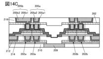
- 14A to 14C are cross-sectional views illustrating an example of a method for manufacturing a semiconductor device.
- 15A and 15B are cross-sectional views illustrating an example of a method for manufacturing a semiconductor device.
- 16A and 16B are cross-sectional views illustrating an example of a method for manufacturing a semiconductor device.
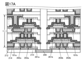
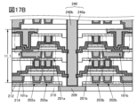
- 17A and 17B are cross-sectional views illustrating an example of a method for manufacturing a semiconductor device.
- 18A and 18B are cross-sectional views illustrating an example of a method for manufacturing a semiconductor device.
- 19A and 19B are diagrams illustrating examples of storage devices.
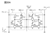
- 20A and 20B are circuit diagrams showing examples of memory layers.
- FIG. 21 is a timing chart for explaining an operation example of a memory cell.
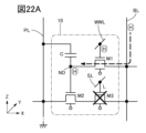
- 22A and 22B are circuit diagrams for explaining an operation example of the memory cell.
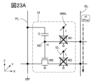
- 23A and 23B are circuit diagrams for explaining an operation example of the memory cell.
- FIG. 24 is a circuit diagram for explaining a configuration example of a semiconductor device.
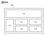
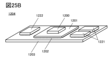
- 25A and 25B are diagrams showing an example of a semiconductor device.
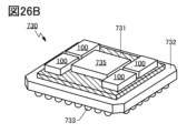
- 26A and 26B are diagrams showing an example of an electronic component.
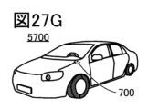
- 27A to 27J are diagrams illustrating examples of electronic devices.
- 28A to 28E are diagrams illustrating examples of electronic devices.
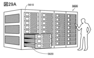
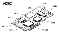
- 29A to 29C are diagrams illustrating examples of electronic devices.
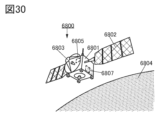
- FIG. 30 is a diagram showing an example of space equipment.
- the ordinal numbers “first” and “second” are used for convenience, and limit the number of constituent elements or the order of constituent elements (for example, the order of steps or the order of stacking). not something to do. Also, the ordinal number given to an element in one place in this specification may not match the ordinal number given to that element elsewhere in the specification or in the claims.
- film and “layer” can be interchanged depending on the case or situation.
- conductive layer can be changed to the term “conductive film.”
- insulating film can be changed to the term “insulating layer”.
- a semiconductor device of one embodiment of the present invention includes a first transistor, a second transistor, and a first insulator over an insulating surface; a first metal oxide on the body and a first conductor on the first metal oxide, the first transistor sharing a second metal oxide on the first metal oxide; and a third conductor on the second insulator, and the second transistor comprises a fourth conductor on the first metal oxide and a third conductor on the second insulator.
- the metal oxide functions as a channel formation region of the first transistor and also functions as a channel formation region of the second transistor.
- the first conductor functions as the source or drain of the first transistor and also functions as the source or drain of the second transistor.
- the transistors can be arranged with high density, and high integration of the semiconductor device can be realized. For example, it can be used for high integration of storage devices such as various memories.
- a semiconductor device of one embodiment of the present invention includes a transistor (OS transistor) including a metal oxide in a channel formation region. Since an OS transistor has a low off-state current, memory content can be retained for a long time by using the OS transistor for a memory device. That is, since the refresh operation is not required or the frequency of the refresh operation is extremely low, the power consumption of the memory device can be sufficiently reduced. Further, since the frequency characteristics of the OS transistor are high, reading from and writing to the memory device can be performed at high speed.
- OS transistor transistor
- a semiconductor device of one embodiment of the present invention includes a first transistor, a second transistor, a third transistor, a first insulator, a second insulator, a third insulator, and a capacitor.
- the first transistor and the second transistor each share a first metal oxide on the first insulator and a first conductor on the first metal oxide;
- the first transistor has a second conductor and a fourth insulator over the first metal oxide and a third conductor over the fourth insulator
- the second transistor has a , a fourth conductor and a fifth insulator on the first metal oxide, and a fifth conductor on the fifth insulator, the third transistor comprising the second metal an oxide, a sixth conductor, a seventh conductor, a sixth insulator over the second metal oxide, and an eighth conductor over the sixth insulator;
- the capacitive element has a ninth conductor, a seventh insulator on the ninth conductor, a tenth conductor on the seventh insulator, and a side surface
- the second conductor and the sixth conductor are electrically connected to each other through openings provided in the second insulator, which are located over the first transistor and the second transistor.
- a third insulator is located over the third transistor, and overlapping portions of the ninth conductor, the seventh insulator, and the tenth conductor are located over the third insulator.
- the sixth conductor and the ninth conductor are electrically connected through an opening provided in the third insulator.
- Openings include, for example, grooves and slits. Also, a region in which an opening is formed may be referred to as an opening.
- drawings used in this embodiment mode show the case where the sidewall of the insulator in the opening of the insulator is substantially perpendicular to the substrate surface or the formation surface, but it may be tapered.
- a tapered shape refers to a shape in which at least part of a side surface of a structure is inclined with respect to a substrate surface or a formation surface.
- a taper angle the angle formed by the inclined side surface and the substrate surface or the formation surface.
- the side surfaces of the structure and the substrate surface are not necessarily completely flat, and may be substantially planar with a fine curvature or substantially planar with fine unevenness.
- a semiconductor device of one embodiment of the present invention is not limited to a structure in which all transistors included in one circuit are formed on the same plane, and for example, a two-stage structure in which the remaining transistors are provided over some of the transistors. can be As a result, the transistors can be arranged with high density, and high integration of the semiconductor device can be realized. For example, it can be used for high integration of storage devices such as various memories.
- a structure in which part of the top surface and part of the side surface of the fourth conductor are directly in contact with the write and read bit lines can be applied.
- a structure in which part of the top surface and part of the side surface of the ninth conductor are directly in contact with the write and read bit lines can be applied.
- the X direction is parallel to the channel length direction of the illustrated transistor
- the Y direction is perpendicular to the X direction
- the Z direction is perpendicular to the X and Y directions.
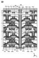
- the semiconductor device shown in FIG. A conductor is provided extending in the Z direction so as to penetrate through n layers (n is an integer of 1 or more) layers 11 (first layer 11_1 to n-th layer 11_n). 209, an insulator 281 over the n-th layer 11_n, an insulator 283 over the insulators 281 and 240, and an insulator and an insulator 285 on the body 283 .
- the components included in the semiconductor device of this embodiment may each have a single-layer structure or a laminated structure.
- the conductor 209 functions as part of circuit elements such as switches, transistors, capacitors, inductors, resistors, and diodes, wirings, electrodes, or terminals.
- FIG. 1 shows a first layer 11_1 that is the bottom layer, a second layer 11_2 on the first layer 11_1, and an nth layer 11_n that is the top layer among the n layers 11. ing.
- the semiconductor device of this embodiment can be used as a memory cell (or memory cell array) of a memory device.
- Each layer of the n layers 11 corresponds to the memory layer 60 in the memory device described in the second embodiment.
- Each layer of the n layers 11 is provided with a memory cell array having a plurality of memory cells.
- the conductor 209 is electrically connected to a driver circuit provided below the conductor 209 for driving the memory cell.
- the first layer 11_1 will be mainly described as an example in the present embodiment.
- the first layer 11_1 includes transistors 201a, 201b, 202a, 202b, 203a, and 203b and capacitors 101a and 101b.
- the configuration on the right side and the configuration on the left side of the conductor 240 are symmetrical. That is, in FIG. 1, the transistors 201a and 201b are symmetrical, the transistors 202a and 202b are symmetrical, the transistors 203a and 203b are symmetrical, and the capacitors 101a and 101b are symmetrical.
- the structure on the left side of the first layer 11_1 (the transistors 201a, 202a, and 203a, and the capacitor 101a) is mainly described as an example.
- the transistor 202a and the transistor 203a are provided over the insulator 214 and share some layers.
- a gate of the transistor 202a and a source or a drain of the transistor 201a are electrically connected to each other through a conductor provided over the transistor 202a.
- One electrode (lower electrode) of the capacitor 101a is physically and electrically connected to the source or drain of the transistor 201a.
- the other electrode (upper electrode) of the capacitor 101a included in the first layer 11_1 is electrically connected to the source or drain of the transistor 202a included in the second layer 11_2.
- the first layer 11_1 has a structure in which two layers provided with transistors are stacked. Specifically, the first layer 11_1 has the transistors 202a and 203a in the first stage (lower stage) and the transistor 201a and the capacitor 101a in the second stage (upper stage). By stacking two layers provided with transistors, the degree of integration can be increased.
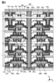
- the semiconductor device shown in FIG. 2 is a modification of the semiconductor device shown in FIG. FIG. 1 shows an example in which the source or drain of the transistor 202a is electrically connected to the conductor 265c; however, as shown in FIG. 2, the conductor 265c may not be provided. In this case, it is preferable that the source or the drain of the transistor 202a is routed in the Y direction so that a desired potential (eg, ground potential) can be easily supplied.
- a desired potential eg, ground potential
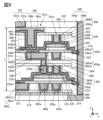
- the semiconductor device shown in FIG. 3 is a modification of the semiconductor device shown in FIG. Specifically, in FIG. 3, the conductor 263 functioning as a contact plug for electrically connecting the gate of the transistor 202a and the source or drain of the transistor 201a is used. In FIG. 3, a contact for electrically connecting the other electrode (upper electrode) of the capacitor 101a included in the first layer 11_1 and the source or drain of the transistor 202a included in the second layer 11_2. A conductor 231 that functions as a plug is used. The conductor 231 is embedded inside an opening provided in an insulator 232 located over the capacitor 101a. Thus, the method of electrically connecting two conductors positioned above and below each other is not particularly limited, and various configurations can be applied.
- FIG. 3 shows an example in which the insulator 212 and the insulator 214 are in contact with the conductor 240.
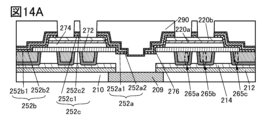
- transistors 202a and 203a are described in detail with reference to FIG.
- the transistor 202a includes a conductor 265b (a conductor 265b1 and a conductor 265b2) provided over the insulator 214, an insulator 272 over the conductor 265b, an insulator 274 over the insulator 272, and an insulator 274 over the insulator 274.
- a conductor 265b (a conductor 265b1 and a conductor 265b2) provided over the insulator 214, an insulator 272 over the conductor 265b, an insulator 274 over the insulator 272, and an insulator 274 over the insulator 274.
- oxide 220 oxide 220 (oxide 220 a and oxide 220 b ), a portion of the side surface of the insulator 274 , and a conductor 252 b (a conductor 252 b 1 and a conductive a conductor 252c (a conductor 252c1 and a conductor 252c2) over oxide 220; an insulator 243b over oxide 220; an insulator 244b over insulator 243b; and a body 270b (a conductor 270b1 and a conductor 270b2).
- the transistor 203a includes a conductor 265a (a conductor 265a1 and a conductor 265a2) provided over the insulator 214, an insulator 272 over the conductor 265a, an insulator 274 over the insulator 272, and a conductor over the insulator 274.
- a conductor 265a (a conductor 265a1 and a conductor 265a2) provided over the insulator 214, an insulator 272 over the conductor 265a, an insulator 274 over the insulator 272, and a conductor over the insulator 274.
- a conductor 252a (a conductor 252a1 and a conductor 252a2) covering part of the side surface of the insulator 274, part of the top surface and part of the side surface of the oxide 220, and an insulator 243a over the oxide 220, an insulator 244a over the insulator 243a, and a conductor 270a (a conductor 270a1 and a conductor 270a2) over the insulator 244a.
- Conductors 265 a and 265 b are embedded inside openings provided in insulator 266 .
- An insulator 276 is provided over the conductors 252 a , 252 b , and 252 c , and an insulator 290 is provided over the insulator 276 .
- Insulators 243 a , 243 b , 244 a , 244 b and conductors 270 a , 270 b are embedded inside openings provided in insulators 290 and 276 .
- the oxide 220 has a region functioning as a channel formation region of the transistor 202a and a region functioning as a channel formation region of the transistor 203a.
- the conductor 252a has a region that functions as one of the source and drain electrodes of the transistor 203a.
- Conductor 252b has a region that functions as one of the source and drain electrodes of transistor 202a.
- the conductor 252c has a region functioning as the other of the source electrode and the drain electrode of the transistor 202a and a region functioning as the other of the source electrode and the drain electrode of the transistor 203a. It can be said that the conductor 252c functions as the other of the source and drain electrodes of the transistor 202a and the other of the source and drain electrodes of the transistor 203a.
- Conductor 270a has a region that functions as a first gate electrode of transistor 203a.
- Insulators 243a and 244a each have a region that functions as a first gate insulator for transistor 203a.
- Conductor 270b has a region that functions as the first gate electrode of transistor 202a.
- Insulators 243b, 244b each have a region that functions as a first gate insulator for transistor 202a.
- Conductor 265a has a region that functions as a second gate electrode of transistor 203a.
- Conductor 265b has a region that functions as a second gate electrode of transistor 202a.
- Insulators 272 and 274 each have a region that functions as a second gate insulator for transistor 202a and a region that functions as a second gate insulator for transistor 203a.
- Transistors 202a and 203a are adjacent and share oxide 220 and conductor 252c, respectively. Accordingly, two transistors (transistor 202a and transistor 203a) can be formed in an area smaller than the area of two transistors (for example, the area of 1.5 transistors). As a result, the transistors can be arranged with high density, and high integration of the semiconductor device can be realized.
- a conductor 252c is arranged in a region between conductors 270a and 270b. Therefore, an n-type region (low-resistance region) can be formed in a region of the oxide 220 (especially the oxide 220b) which overlaps with the conductor 252c.
- current can flow between the transistor 202a and the transistor 203a through the conductor 252c. Therefore, the resistance component between the transistor 202a and the transistor 203a can be significantly reduced compared to a structure in which two transistors (also referred to as Si transistors) using silicon for a semiconductor layer in which a channel is formed are connected in series. .
- the structures of the transistor 202a and the transistor 203a are similar to that of the transistor 201a except that the oxide 220 and the conductor 252c are shared. Materials and manufacturing methods that can be applied to the transistors 202a and 203a are also the same as those of the transistor 201a. Therefore, the material and manufacturing method of the transistor included in the semiconductor device of this embodiment will be collectively described when the transistor 201a is described later.
- FIG. 5 shows an enlarged view of the configuration of the left half of the first layer 11_1 in FIG. 3 (the conductor 240 and the configuration shown to the left thereof).
- the transistor 202 a and the transistor 203 a are provided over the insulator 214 .
- a conductor 252b included in the transistor 202a is electrically connected to the conductor 265c (the conductor 265c1 and the conductor 265c2).
- An insulator 262 is provided over the insulator 290 , the transistor 202 a , and the transistor 203 a , and an insulator 264 is provided over the insulator 262 .
- Conductors 263 (conductors 263 a and 263 b ) are provided inside openings provided in the insulators 262 and 264 .
- a transistor 201 a and a capacitor 101 a are provided over the insulator 264 .
- the transistor 201a includes the conductor 205a (the conductor 205a1 and the conductor 205a2) provided over the insulator 264, the insulator 222 over the conductor 205a, the insulator 224 over the insulator 222, and the insulator 224 over the insulator 224.
- oxide 230 oxide 230a and oxide 230b
- a conductor 242a conductor 242a1 and conductor 242a2 and conductor 242b
- conductor 242b conductor 242b1 and conductor 242b2
- insulator 253 on oxide 230 insulator 254 on insulator 253, conductor 260 on insulator 254 ( a conductor 260a and a conductor 260b).
- Conductors 205 a and 205 b are embedded inside openings provided in insulator 216 .
- An insulator 275 is provided over the conductors 242 a and 242 b
- an insulator 280 is provided over the insulator 275 .
- the insulators 253 and 254 and the conductor 260 are embedded inside openings provided in the insulator 280 and the insulator 275 .
- An insulator 282 is provided over the insulator 280 and the conductor 260 .
- Oxide 230 has a region that functions as a channel formation region of transistor 201a.
- the conductor 242a has a region that functions as one of the source and drain electrodes of the transistor 201a.
- the conductor 242b has a region that functions as the other of the source and drain electrodes of the transistor 201a.
- Conductor 260 has a region that functions as a first gate electrode of transistor 201a.
- Insulators 253, 254 each have a region that functions as a first gate insulator for transistor 201a.
- Conductor 205a has a region that functions as a second gate electrode of transistor 201a.
- Insulators 222, 224 each have a region that functions as a second gate insulator for transistor 201a.
- a conductor 242b included in the transistor 201a is electrically connected to a conductor 270b included in the transistor 202a.
- the conductor 242 b is electrically connected to the conductor 270 b through the conductor 205 b (the conductor 205 b 1 and the conductor 205 b 2 ) and the conductor 263 .
- the capacitor 101a includes the conductor 153 over the conductor 242b, the insulator 154 over the conductor 153, and the conductor 160 over the insulator 154 (the conductor 160a and the conductor 160b).
- At least part of the conductor 153 , the insulator 154 , and the conductor 160 are arranged inside openings provided in the insulators 275 , 280 , and 282 .
- Each end of conductor 153 , insulator 154 , and conductor 160 rests on insulator 282 .
- the insulator 154 is provided so as to cover the end of the conductor 153 .
- the conductor 153 and the conductor 160 can be electrically insulated.
- the capacitance element 101a increases. can increase the capacitance of By increasing the capacitance per unit area of the capacitor 101a, miniaturization or high integration of the semiconductor device can be achieved.
- a conductor 231 (a conductor 231a and a conductor 231b) is provided over the conductor 160 to electrically connect the conductor 160 and the source or drain of the upper transistor 202a. can be connected. Note that as shown in FIG. 1, the conductor 160 can be electrically connected to the source or drain of the upper transistor 202a without the conductor 231 interposed therebetween.
- the conductor 153 has a region functioning as one electrode (lower electrode) of the capacitor 101a.
- the insulator 154 has a region functioning as a dielectric of the capacitor 101a.
- the conductor 160 has a region that functions as the other electrode (upper electrode) of the capacitor 101a.
- the capacitive element 101a constitutes an MIM (Metal-Insulator-Metal) capacitor.
- Conductor 242a which includes a region that functions as one of the source or drain electrodes of transistor 201a, extends beyond oxide 230, which functions as a semiconductor layer. Therefore, the conductor 242a also functions as a wiring. For example, in FIG. 5, a portion of each of the top, side, and bottom surfaces of conductor 242a is electrically connected to conductor 240 extending in the Z direction.
- conductor 252a which includes a region that functions as one of the source or drain electrodes of transistor 203a, extends beyond oxide 220, which functions as a semiconductor layer. Therefore, the conductor 252a also functions as a wiring. For example, in FIG. 5, a portion of each of the top, side, and bottom surfaces of conductor 252a is electrically connected to conductor 240 extending in the Z direction.
- the conductor 240 is in direct contact with at least one of the top surface, the side surface, and the bottom surface of the conductor 242a and at least one of the top surface, the side surface, and the bottom surface of the conductor 252a, so that an electrode for connection is separately provided. Since it is not necessary, the area occupied by the memory cell array can be reduced. Also, the degree of integration of memory cells is improved, and the storage capacity can be increased. Note that the conductor 240 is preferably in contact with two or more of the top surface, the side surface, and the bottom surface of the conductor 242a. Similarly, conductor 240 preferably contacts two or more of the top, side, and bottom surfaces of conductor 252a. The contact resistance between the conductor 240 and the conductor 242a or the conductor 252a can be reduced when the conductor 240 is in contact with the conductor 242a or multiple surfaces of the conductor 252a.
- FIG. 6 shows an enlarged view of a region where the conductor 240 and the conductor 242a are in contact with each other and its vicinity.
- conductor 240 has a region with width W1 and a region with width W2.
- the width W1 corresponds to the distance between the conductor 242a of the transistor 201a and the conductor 242a of the transistor 201b.
- the width W2 corresponds to, for example, the distance between the interface between the insulator 280 and the conductor 240a on the transistor 201a side and the interface between the insulator 280 and the conductor 240a on the transistor 201b side.
- width W2 is preferably greater than width W1.
- the conductor 240 is in contact with at least part of the top surface and part of the side surface of the conductor 242a. Therefore, the area of the region where the conductor 240 and the conductor 242a are in contact can be increased. Note that in this specification and the like, the contact between the conductor 240 and the conductor 242a is sometimes called a topside contact. Also, as shown in FIG. 6, the conductor 240 may contact a portion of the lower surface of the conductor 242a. With this structure, the area of the region where the conductor 240 and the conductor 242a are in contact can be further increased.
- the ends of insulator 262 are positioned inwardly of the respective ends of insulators 266, 290, 264, 216, 280, 284, and 232.
- the ends of insulator 282 are positioned inwardly of the respective ends of insulators 266, 290, 264, 216, 280, 284, and 232.
- the ends of insulator 262 and the ends of insulator 282 may be closer than one or more of insulators 266, 290, 264, 216, 280, 284, 232, respectively. can also be applied inwardly.
- insulators 266, 290, 264, 216, 280, 284 and 232 respectively function as interlayer films.
- insulators 266, 290, 264, 216, 280, 284, and 232 each preferably comprise one or both of silicon oxide and silicon oxynitride.
- oxynitride refers to a material whose composition contains more oxygen than nitrogen
- nitride oxide refers to a material whose composition contains more nitrogen than oxygen. point to the material.
- silicon oxynitride refers to a material whose composition contains more oxygen than nitrogen
- silicon nitride oxide refers to a material whose composition contains more nitrogen than oxygen. indicates
- the insulator 262 and the insulator 282 preferably function as barrier insulators of the transistor.
- insulator 262 and insulator 282 preferably comprise one or both of aluminum oxide and hafnium oxide, respectively.
- a barrier insulator refers to an insulator having a barrier property.
- the term "barrier property” refers to a function of suppressing diffusion of a corresponding substance (also referred to as low permeability).
- the corresponding substance has the function of capturing and fixing (also called gettering).
- aluminum oxide and hafnium oxide may be more difficult to etch than silicon oxide or silicon oxynitride. It can also be said that aluminum oxide and hafnium oxide are each difficult-to-etch materials.
- an opening needs to be provided in the stacked structure of the insulators before the conductor 240 is provided.
- the insulators 266, 290, 264, 216, 280, and 284 are made of materials that are easier to etch than the insulators 262 and 282.
- An opening is provided in an insulator using In this way, the insulator using the hard-to-etch material is opened in advance, and the other insulators are opened together before the conductor 240 is provided, so that the process margin can be increased. Moreover, the yield in forming each opening can be increased, and the productivity of the semiconductor device can be improved.
- recesses are provided in a region of the insulator 280 that does not overlap with the insulator 282 and a region of the insulator 290 that does not overlap with the insulator 262 .
- part of the insulator 280 or the insulator 290 may be removed during processing of the insulator 282 or the insulator 262 to form a recess. Note that the insulators 280 and 290 do not have to have recesses.
- the ends of the insulator 262 are located outside the respective ends of the insulators 266 , 290 , 264 , 216 , 280 , 284 and 232 .
- the ends of insulator 282 are located outside the respective ends of insulators 266 , 290 , 264 , 216 , 280 , 284 , 232 .
- the ends of insulator 262 and the ends of insulator 282 are positioned outwardly from the ends of one or more of insulators 266, 290, 264, 216, 280, 284, and 232, respectively. configuration can be applied.
- the opening when an opening for providing the conductor 240 is provided in the laminated structure of the insulator after n layers of memory cells are stacked, the opening must be deep. It may be difficult to keep the width of (also referred to as the opening diameter, corresponding to the length in the X-axis direction in FIG. 1 and the like) constant. For example, the width of the upper side (nth layer side) of the opening tends to be wide, and the width of the lower side (first layer side) of the opening tends to be narrow.
- the end portion of the insulator 262 and the end portion of the insulator 282 are provided so as to protrude into the opening, excessive etching of the opening can be suppressed in some cases. As a result, variations in opening diameter can be suppressed. In addition, it is possible to secure a sufficient width at the bottom of the opening while preventing the width of the top of the opening from being too wide.
- FIGS. 7 and 8 show examples in which the ends of the insulator 262 and the ends of the insulator 282 are aligned or substantially aligned with the ends of the conductor 242a and the conductor 252a. . Also, FIG. 8 shows an example in which the ends of the insulator 272 and the ends of the insulator 222 are substantially aligned with the ends of the conductor 242a and the conductor 252a.
- the semiconductor device of one embodiment of the present invention is not limited to these structures.
- the ends of each of the insulators 272, 222, 262, 282 may be positioned more outwardly than the ends of the conductors 242a and/or the ends of the conductors 252a, and may be positioned inwardly. good too.
- the contours between the laminated layers are in a top view. It can be said that some overlap.
- Such a case includes, for example, the case where the upper layer and the lower layer are processed with the same mask pattern or partially with the same mask pattern. Strictly speaking, however, the contours do not overlap, and part of the top layer may be located inside the bottom layer, or part of the top layer may be located outside the bottom layer. or that the top surface shapes are substantially the same.
- the ends of the insulators 222 and 272 are located inside the ends of the insulators 266, 290, 264, 216, 280, 284, and 232, respectively.
- the configurations of the insulator 222 and the insulator 272 are not limited to this.
- the ends of insulator 222 and the ends of insulator 272 are located outside the respective ends of insulators 266, 290, 264, 216, 280, 284, and 232, respectively.
- the conductor 240 when the end portion of the insulator 272 is located inside the end portion of the conductor 252a, the conductor 240 may be in contact with the top surface, side surfaces, and bottom surface of the conductor 252a. Therefore, the contact resistance between the conductor 240 and the conductor 252a can be reduced. Similarly, when the end of the insulator 222 is located inside the end of the conductor 242a, the conductor 240 can be in contact with the top surface, the side surface, and the bottom surface of the conductor 242a. The contact resistance between 240 and conductor 242a can be reduced.
- recesses are provided in a region of the insulator 216 that does not overlap with the insulator 222 and a region of the insulator 266 that does not overlap with the insulator 272 .
- part of the insulator 216 or the insulator 266 may be removed and a recess may be formed when the insulator 222 or the insulator 272 is processed. Note that the insulators 216 and 266 do not have to have recesses.
- the insulator 266 can be configured without a recess.
- the edge of insulator 222 is generally aligned with the edge of conductor 242a or positioned outside the edge of conductor 242a, insulator 216 will be recessed in the completed semiconductor device. can be configured without In some cases, the shape of the concave portion provided in the insulator tends to vary. Therefore, by leaving no recesses in the insulators 266 and 216, variation in the shape of the semiconductor device can be reduced.
- the method for realizing the configurations shown in FIGS. 5, 7, and 8 is not limited to this.
- the insulator 282 and the insulator 280 have different etching rates, even if the insulator 282 and the insulator 280 are opened together, the edges of the insulator 282 and the insulator 280 may not be aligned in a cross-sectional view.
- insulators 282 and 280 may be opened together to form insulators 280 and 282 having the shape shown in FIG.
- a semiconductor device manufactured by such a method is also included in one embodiment of the present invention.
- insulators 262, 282, 266, 290, 264, 216, 280, and 284 are also described below.
- the components of the transistor 201a are mainly described as an example, but the components of the transistors 202a and 203a can also be applied.
- the descriptions of conductor 205, insulator 222, insulator 224, oxide 230, conductor 242, insulator 253, insulator 254, and conductor 260 refer to conductor 265, insulator 272, insulator 274, oxide 220, conductor 252, insulator 243, insulator 244, and conductor 270.
- Oxide 230 preferably comprises oxide 230a over insulator 224 and oxide 230b over oxide 230a. By providing the oxide 230a under the oxide 230b, diffusion of impurities from a structure formed below the oxide 230a to the oxide 230b can be suppressed.
- the oxide 230 has a two-layer structure of the oxide 230a and the oxide 230b is described in this embodiment, the structure is not limited to this.
- the oxide 230 may have, for example, a single-layer structure of the oxide 230b or a stacked structure of three or more layers.
- the oxide 230b includes a channel formation region and source and drain regions provided to sandwich the channel formation region in the transistor 201a. At least part of the channel formation region overlaps the conductor 260 . One of the source and drain regions overlaps the conductor 242a and the other overlaps the conductor 242b.
- the channel formation region is a high-resistance region with a low carrier concentration because it has less oxygen vacancies or a lower impurity concentration than the source and drain regions. Therefore, the channel forming region can be said to be i-type (intrinsic) or substantially i-type.
- the source region and the drain region are low-resistance regions with high carrier concentration because they have many oxygen vacancies or have a high concentration of impurities such as hydrogen, nitrogen, and metal elements. That is, the source region and the drain region are n-type regions (low resistance regions) having a higher carrier concentration than the channel forming region.
- the carrier concentration of the channel formation region is 1 ⁇ 10 18 cm ⁇ 3 or less, less than 1 ⁇ 10 17 cm ⁇ 3 , less than 1 ⁇ 10 16 cm ⁇ 3 , less than 1 ⁇ 10 15 cm ⁇ 3 , and 1 ⁇ 10 14 .
- cm ⁇ 3 less than 1 ⁇ 10 13 cm ⁇ 3 , less than 1 ⁇ 10 12 cm ⁇ 3 , less than 1 ⁇ 10 11 cm ⁇ 3 , or less than 1 ⁇ 10 10 cm ⁇ 3 .
- the lower limit of the carrier concentration in the channel forming region is not particularly limited, but can be, for example, 1 ⁇ 10 ⁇ 9 cm ⁇ 3 .
- the impurity concentration in the oxide 230b is lowered to lower the defect level density.
- a low impurity concentration and a low defect level density are referred to as high-purity intrinsic or substantially high-purity intrinsic.
- an oxide semiconductor (or metal oxide) with a low carrier concentration is sometimes referred to as a highly purified intrinsic or substantially highly purified intrinsic oxide semiconductor (or metal oxide).
- Reducing the impurity concentration in the oxide 230b is effective in stabilizing the electrical characteristics of the transistor 201a. Moreover, in order to reduce the impurity concentration of the oxide 230b, it is preferable to reduce the impurity concentration in adjacent films as well.
- Impurities include hydrogen, nitrogen, alkali metals, alkaline earth metals, iron, nickel, silicon, and the like.
- the impurities in the oxide 230b refer to, for example, substances other than the main components of the oxide 230b. For example, an element with a concentration of less than 0.1 atomic percent can be considered an impurity.
- the channel formation region, the source region, and the drain region may each be formed up to the oxide 230a in addition to the oxide 230b.
- concentrations of metal elements and impurity elements such as hydrogen and nitrogen detected in each region are not limited to stepwise changes for each region, and may change continuously within each region. That is, the closer the region is to the channel formation region, the lower the concentrations of the metal element and the impurity element such as hydrogen and nitrogen may be.
- a metal oxide that functions as a semiconductor (hereinafter also referred to as an oxide semiconductor) is preferably used for the oxide 230 (the oxide 230a and the oxide 230b).
- the bandgap of the metal oxide functioning as a semiconductor is preferably 2 eV or more, more preferably 2.5 eV or more.
- the off-state current of the transistor can be reduced by using a metal oxide with a large bandgap.
- Metal oxides such as indium oxide, gallium oxide, and zinc oxide are preferably used as the oxide 230 .
- the oxide 230 it is preferable to use, for example, a metal oxide containing two or three elements selected from indium, the element M, and zinc.
- Element M includes gallium, aluminum, silicon, boron, yttrium, tin, copper, vanadium, beryllium, titanium, iron, nickel, germanium, zirconium, molybdenum, lanthanum, cerium, neodymium, hafnium, tantalum, tungsten, and magnesium.
- the element M is preferably one or more selected from aluminum, gallium, yttrium, and tin.
- a metal oxide containing indium, the element M, and zinc is sometimes referred to as an In-M-Zn oxide.
- the oxide 230 preferably has a laminated structure of multiple oxide layers with different chemical compositions.
- the atomic ratio of the element M to the main component metal element is the same as the atomic ratio of the element M to the main component metal element in the metal oxide used for the oxide 230b. Larger is preferable.
- the atomic ratio of the element M to In is preferably higher than the atomic ratio of the element M to In in the metal oxide used for the oxide 230b. With this structure, diffusion of impurities and oxygen from structures formed below the oxide 230a to the oxide 230b can be suppressed.
- the atomic ratio of In to the element M in the metal oxide used for the oxide 230b is preferably higher than the atomic ratio of In to the element M in the metal oxide used for the oxide 230a.
- the transistor 201a can have high on-state current and high frequency characteristics.
- the oxide 230a and the oxide 230b contain a common element other than oxygen as a main component, the defect level density at the interface between the oxide 230a and the oxide 230b can be reduced. Therefore, the influence of interface scattering on carrier conduction is reduced, and the transistor 201a can obtain a large on-state current and high frequency characteristics.
- the neighboring composition includes a range of ⁇ 30% of the desired atomic number ratio.
- the element M it is preferable to use gallium.
- a metal oxide that can be used for the oxide 230a may be used as the oxide 230b.
- the above atomic ratio is not limited to the atomic ratio of the deposited metal oxide, and the atomic ratio of the sputtering target used for the deposition of the metal oxide. may be
- the oxide 230b preferably has crystallinity.
- CAAC-OS c-axis aligned crystal oxide semiconductor
- CAAC-OS is a metal oxide that has a dense structure with high crystallinity and few impurities and defects (eg, oxygen vacancies).
- heat treatment is performed at a temperature at which the metal oxide is not polycrystallized (for example, 400° C. or more and 600° C. or less), so that the CAAC-OS has a dense structure with higher crystallinity.
- a temperature at which the metal oxide is not polycrystallized for example, 400° C. or more and 600° C. or less
- CAAC-OS since it is difficult to confirm a clear crystal grain boundary in CAAC-OS, it can be said that a decrease in electron mobility due to a crystal grain boundary is unlikely to occur. Therefore, metal oxides with CAAC-OS have stable physical properties. Therefore, a metal oxide including CAAC-OS is heat resistant and highly reliable.
- the oxide 230b by using a crystalline oxide such as CAAC-OS as the oxide 230b, extraction of oxygen from the oxide 230b by the source electrode or the drain electrode can be suppressed. Accordingly, extraction of oxygen from the oxide 230b can be reduced even if heat treatment is performed, so that the transistor 201a is stable against high temperatures (so-called thermal budget) in the manufacturing process.
- a crystalline oxide such as CAAC-OS
- a transistor including an oxide semiconductor if impurities and oxygen vacancies are present in a region where a channel is formed in the oxide semiconductor, electrical characteristics are likely to vary, and reliability may be degraded.
- hydrogen in the vicinity of oxygen vacancies may form defects in which hydrogen enters oxygen vacancies (hereinafter sometimes referred to as V OH ) to generate electrons serving as carriers. Therefore, if oxygen vacancies are included in the region where the channel is formed in the oxide semiconductor, the transistor has normally-on characteristics (a channel exists even if no voltage is applied to the gate electrode, and current flows through the transistor). flow characteristics). Therefore, impurities, oxygen vacancies, and VOH are preferably reduced as much as possible in a region where a channel is formed in the oxide semiconductor. In other words, the region in which the channel is formed in the oxide semiconductor preferably has a reduced carrier concentration and is i-type (intrinsic) or substantially i-type.
- an insulator containing oxygen that is released by heating (hereinafter sometimes referred to as excess oxygen) is provided in the vicinity of the oxide semiconductor, and heat treatment is performed so that the oxide semiconductor is converted from the insulator.
- Oxygen can be supplied and oxygen vacancies and VOH can be reduced.
- the on-state current or the field-effect mobility of the transistor 201a might decrease.
- variations in the amount of oxygen supplied to the source region or the drain region within the substrate surface cause variations in the characteristics of the semiconductor device having transistors.
- the conductor when oxygen supplied from the insulator to the oxide semiconductor diffuses into a conductor such as a gate electrode, a source electrode, or a drain electrode, the conductor is oxidized and the conductivity is impaired.
- the electrical characteristics and reliability of the transistor may be adversely affected.
- the channel formation region preferably has a reduced carrier concentration and is i-type or substantially i-type, while the source region and the drain region have a high carrier concentration and are n-type. is preferred.
- oxygen vacancies and V OH in the channel formation region of the oxide semiconductor are preferably reduced.
- the semiconductor device is configured such that the hydrogen concentration in the channel formation region is reduced, the oxidation of the conductors 242a, 242b, and 260 is suppressed, and the It is configured to suppress the decrease in the hydrogen concentration of.
- the insulator 253 in contact with the channel formation region in the oxide 230b preferably has a function of trapping hydrogen and fixing hydrogen. Thereby, the hydrogen concentration in the channel formation region of the oxide 230b can be reduced. Therefore, V OH in the channel formation region can be reduced, and the channel formation region can be i-type or substantially i-type.
- a metal oxide having an amorphous structure is given as an insulator having a function of trapping and fixing hydrogen.
- the insulator 253 for example, magnesium oxide or a metal oxide such as an oxide containing one or both of aluminum and hafnium is preferably used. Oxygen atoms in metal oxides having such an amorphous structure have dangling bonds, and the dangling bonds sometimes have the property of capturing or fixing hydrogen. That is, it can be said that a metal oxide having an amorphous structure has a high ability to capture or fix hydrogen.
- a high dielectric constant (high-k) material for the insulator 253 .
- An example of a high-k material is an oxide containing one or both of aluminum and hafnium.
- an oxide containing one or both of aluminum and hafnium is preferably used as the insulator 253, and an oxide having an amorphous structure and containing one or both of aluminum and hafnium is more preferably used. It is more preferable to use hafnium oxide having a structure.
- hafnium oxide is used as the insulator 253 .
- the insulator 253 is an insulator containing at least oxygen and hafnium.
- the hafnium oxide has an amorphous structure.
- insulator 253 has an amorphous structure.
- an insulator having a structure stable against heat such as silicon oxide or silicon oxynitride
- the insulator 253 may be a stacked structure including aluminum oxide and silicon oxide or silicon oxynitride over the aluminum oxide.
- the insulator 253 may be a stacked-layer structure including aluminum oxide, silicon oxide or silicon oxynitride over aluminum oxide, and hafnium oxide over silicon oxide or silicon oxynitride.
- barrier insulators against oxygen are preferably provided near the conductors 242a, 242b, and 260, respectively.
- the insulators are the insulators 253, 254, and 275, for example.
- Barrier insulators against oxygen include, for example, oxides containing one or both of aluminum and hafnium, magnesium oxide, gallium oxide, indium gallium zinc oxide, silicon nitride, and silicon oxynitride.
- oxides containing one or both of aluminum and hafnium include aluminum oxide, hafnium oxide, oxides containing aluminum and hafnium (hafnium aluminate), and oxides containing hafnium and silicon (hafnium silicate). mentioned.
- each of the insulator 253, the insulator 254, and the insulator 275 preferably has a single-layer structure or a laminated structure of barrier insulators against oxygen.
- the insulator 253 preferably has a barrier property against oxygen. It is preferable that the insulator 253 is at least less permeable to oxygen than the insulator 280 .
- the insulator 253 has regions in contact with the side surface of the conductor 242a and the side surface of the conductor 242b. Since the insulator 253 has a barrier property against oxygen, the side surfaces of the conductors 242a and 242b are oxidized and formation of an oxide film on the side surfaces can be suppressed. Accordingly, reduction in on-state current or reduction in field-effect mobility of the transistor 201a can be suppressed.
- the insulator 253 is provided in contact with the top surface and side surfaces of the oxide 230b, the side surfaces of the oxide 230a, the side surface of the insulator 224, and the top surface of the insulator 222. Since the insulator 253 has a barrier property against oxygen, oxygen can be prevented from being released from the channel formation region of the oxide 230b when heat treatment or the like is performed. Therefore, formation of oxygen vacancies in the oxides 230a and 230b can be reduced.
- the insulator 280 contains an excessive amount of oxygen, excessive supply of the oxygen to the oxides 230a and 230b can be suppressed. Therefore, excessive oxidation of the source region and the drain region and reduction in on-state current or reduction in field-effect mobility of the transistor 201a can be suppressed.
- An oxide containing one or both of aluminum and hafnium can be suitably used as the insulator 253 because it has a barrier property against oxygen.
- the insulator 254 preferably has a barrier property against oxygen.
- the insulator 254 is provided between the channel forming region of the oxide 230 and the conductor 260 and between the insulator 280 and the conductor 260 . With this structure, diffusion of oxygen contained in the channel formation region of the oxide 230 into the conductor 260 and formation of oxygen vacancies in the channel formation region of the oxide 230 can be suppressed. In addition, oxygen contained in the oxide 230 and oxygen contained in the insulator 280 diffuse into the conductor 260, so that oxidation of the conductor 260 can be suppressed.
- the insulator 254 is preferably at least less permeable to oxygen than the insulator 280 .
- silicon nitride is preferably used as the insulator 254 .
- the insulator 254 is an insulator containing at least nitrogen and silicon.
- the insulator 254 preferably has a barrier property against hydrogen. Accordingly, impurities such as hydrogen contained in the conductor 260 can be prevented from diffusing into the oxide 230b.
- the insulator 275 preferably has a barrier property against oxygen.
- the insulator 275 is provided between the insulator 280 and the conductor 242a and between the insulator 280 and the conductor 242b. With this structure, diffusion of oxygen contained in the insulator 280 to the conductors 242a and 242b can be suppressed. Therefore, it is possible to prevent the conductors 242a and 242b from being oxidized by oxygen contained in the insulator 280 to increase the resistivity and reduce the on-state current. It is preferable that the insulator 275 is at least less permeable to oxygen than the insulator 280 .
- silicon nitride is preferably used as the insulator 275 .
- the insulator 275 is an insulator containing at least nitrogen and silicon.
- the barrier insulator against hydrogen is the insulator 275, for example.
- Barrier insulators to hydrogen include oxides such as aluminum oxide, hafnium oxide, tantalum oxide, and nitrides such as silicon nitride.
- the insulator 275 preferably has a single-layer structure or a laminated structure of the barrier insulator against hydrogen.
- the insulator 275 preferably has a barrier property against hydrogen. Since the insulator 275 has a barrier property against hydrogen, the insulator 253 can suppress capture and fixation of hydrogen in the source and drain regions. Therefore, the source and drain regions can be n-type.
- the channel formation region can be i-type or substantially i-type
- the source region and the drain region can be n-type
- a semiconductor device having good electrical characteristics can be provided. Further, with the above structure, even if the semiconductor device is miniaturized or highly integrated, it can have good electrical characteristics. Further, by miniaturizing the transistor 201a, high frequency characteristics can be improved. Specifically, the cutoff frequency can be improved.
- Insulator 253 and insulator 254 each function as part of the gate insulator.
- the insulators 253 and 254 are provided in openings formed in the insulator 280 or the like together with the conductor 260 . It is preferable that the thickness of the insulator 253 and the thickness of the insulator 254 be small in order to miniaturize the transistor 201a.
- the thickness of the insulator 253 is preferably 0.1 nm or more and 5.0 nm or less, more preferably 0.5 nm or more and 5.0 nm or less, more preferably 1.0 nm or more and less than 5.0 nm, and 1.0 nm or more and 3.0 nm.
- the thickness of the insulator 254 is preferably 0.1 nm to 5.0 nm, more preferably 0.5 nm to 3.0 nm, even more preferably 1.0 nm to 3.0 nm. Note that each of the insulators 253 and 254 may have at least a part of the region with the thickness as described above.
- the ALD method includes a thermal ALD (thermal ALD) method in which a precursor and a reactant react with only thermal energy, a PEALD (plasma enhanced ALD) method using a plasma-excited reactant, and the like.
- thermal ALD thermal ALD
- PEALD plasma enhanced ALD
- film formation can be performed at a lower temperature by using plasma, which is preferable in some cases.
- the ALD method can deposit atoms one layer at a time, it is possible to form extremely thin films, to form structures with a high aspect ratio, to form films with few defects such as pinholes, and to improve coverage. There are effects such as excellent film formation and low temperature film formation. Therefore, the insulator 253 can be formed with a thin film thickness as described above with good coverage on the side surfaces of the opening formed in the insulator 280 and the like, the side ends of the conductors 242a and 242b, and the like. .
- a film formed by the ALD method may contain more impurities such as carbon than films formed by other film formation methods.
- quantification of impurities secondary ion mass spectrometry (SIMS: Secondary Ion Mass Spectrometry), X-ray photoelectron spectroscopy (XPS: X-ray Photoelectron Spectroscopy), or Auger electron spectroscopy (AES: Auger Electron Spectroscopy) can be performed using
- silicon nitride deposited by a PEALD method can be used as the insulator 254 .
- the insulator 253 can also function as the insulator 254 .
- the structure without the insulator 254 can simplify the manufacturing process of the semiconductor device and improve productivity.
- the semiconductor device preferably has a structure in which entry of hydrogen into the transistor 201a is suppressed.
- an insulator having a function of suppressing diffusion of hydrogen is preferably provided so as to cover one or both of the top and bottom of the transistor 201a.
- the insulator is the insulator 212, for example.
- An insulator having a function of suppressing diffusion of hydrogen is preferably used as the insulator 212 . Accordingly, diffusion of hydrogen from below the insulator 212 to the transistor 201a can be suppressed.
- the insulator 212 any of the insulators that can be used for the insulator 275 can be used.
- One or more of the insulator 212, the insulator 214, the insulator 262, the insulator 282, the insulator 283, the insulator 284, and the insulator 285 is exposed to impurities such as water and hydrogen from the substrate side or It preferably functions as a barrier insulator that suppresses diffusion from above the transistor 201a to the transistor 201a.
- one or more of insulator 212, insulator 214, insulator 262, insulator 282, insulator 283, insulator 284, and insulator 285 are hydrogen atoms, hydrogen molecules, water molecules, nitrogen atoms. It is preferable to have an insulating material that has a function of suppressing the diffusion of impurities such as nitrogen molecules, nitrogen oxide molecules (N 2 O, NO, NO 2 , etc.), and copper atoms (the above impurities are difficult to permeate). Alternatively, it is preferable to use an insulating material that has a function of suppressing diffusion of oxygen (eg, at least one of oxygen atoms and oxygen molecules) (through which oxygen hardly permeates).
- oxygen eg, at least one of oxygen atoms and oxygen molecules
- the insulator 212, the insulator 214, the insulator 262, the insulator 282, the insulator 283, the insulator 284, and the insulator 285 are insulators each having a function of suppressing diffusion of water, impurities such as hydrogen, and oxygen. It preferably has a body, and for example, aluminum oxide, magnesium oxide, hafnium oxide, gallium oxide, indium gallium zinc oxide, silicon nitride, or silicon nitride oxide can be used.
- the insulator 212 is preferably made of silicon nitride or the like, which has a higher hydrogen barrier property.
- the insulator 214, the insulator 262, the insulator 282, the insulator 283, the insulator 284, and the insulator 285 are aluminum oxide, magnesium oxide, or the like, each of which has a high function of capturing hydrogen and fixing hydrogen. It is preferred to have Accordingly, diffusion of impurities such as water and hydrogen from the substrate side to the transistor 201a side through the insulators 212 and 214 can be suppressed. Alternatively, impurities such as water and hydrogen can be prevented from diffusing toward the transistor 201a from an interlayer insulating film or the like arranged outside the insulator 284 . Alternatively, diffusion of oxygen contained in the insulator 224 or the like to the substrate side can be suppressed.
- oxygen contained in the insulator 280 or the like can be prevented from diffusing upward from the transistor 201a through the insulator 282 or the like.
- the conductor 205 a is arranged to overlap with the oxide 230 and the conductor 260 .
- the conductor 205a is preferably embedded in an opening formed in the insulator 216 .
- part of the conductor 205a is embedded in the insulator 214 in some cases.
- the conductor 205a may have a single-layer structure or a laminated structure.
- the conductor 205a has a conductor 205a1 and a conductor 205a2.
- the conductor 205a1 is provided in contact with the bottom surface and side walls of the opening.
- the conductor 205a2 is provided so as to be embedded in the recess of the conductor 205a1.
- the height of the top surface of the conductor 205 a 2 approximately matches the height of the top surface of the conductor 205 a 1 and the height of the top surface of the insulator 216 .
- the conductor 205a1 has a function of suppressing diffusion of impurities such as hydrogen atoms, hydrogen molecules, water molecules, nitrogen atoms, nitrogen molecules, nitrogen oxide molecules (such as N 2 O, NO, NO 2 ), and copper atoms. It is preferable to have a conductive material with Alternatively, a conductive material having a function of suppressing diffusion of oxygen (eg, at least one of oxygen atoms and oxygen molecules) is preferably included.
- a conductive material having a function of reducing diffusion of hydrogen When a conductive material having a function of reducing diffusion of hydrogen is used for the conductor 205a1, impurities such as hydrogen contained in the conductor 205a2 enter the oxide 230 through the insulators 216, 224, and the like. You can prevent it from spreading.
- a conductive material having a function of suppressing diffusion of oxygen for the conductor 205a1, it is possible to suppress oxidation of the conductor 205a2 and a decrease in conductivity.
- Examples of conductive materials having a function of suppressing diffusion of oxygen include titanium, titanium nitride, tantalum, tantalum nitride, ruthenium, and ruthenium oxide.
- the conductor 205a1 can have a single-layer structure or a laminated structure of any of the above conductive materials.
- conductor 205a1 preferably comprises titanium nitride.
- a conductive material containing tungsten, copper, or aluminum as its main component is preferably used for the conductor 205a2.
- conductor 205a2 preferably comprises tungsten.
- the conductor 205a can function as a second gate electrode.
- the potential applied to the conductor 205a is changed independently of the potential applied to the conductor 260, so that the threshold voltage (Vth) of the transistor 201a can be controlled.
- Vth threshold voltage
- the Vth of the transistor 201a can be increased and the off current can be reduced. Therefore, applying a negative potential to the conductor 205a can make the drain current smaller when the potential applied to the conductor 260 is 0 V than when no potential is applied.
- the electric resistivity of the conductor 205a is designed in consideration of the potential applied to the conductor 205a, and the film thickness of the conductor 205a is set according to the electric resistivity.
- the film thickness of the insulator 216 is almost the same as that of the conductor 205a.
- Insulator 222 and insulator 224 function as gate insulators.
- the insulator 222 preferably has a function of suppressing diffusion of hydrogen (eg, at least one of hydrogen atoms and hydrogen molecules). Further, the insulator 222 preferably has a function of suppressing diffusion of oxygen (eg, at least one of oxygen atoms and oxygen molecules). For example, the insulator 222 preferably has a function of suppressing diffusion of one or both of hydrogen and oxygen more than the insulator 224 does.
- hydrogen eg, at least one of hydrogen atoms and hydrogen molecules
- oxygen eg, at least one of oxygen atoms and oxygen molecules
- the insulator 222 preferably has a function of suppressing diffusion of one or both of hydrogen and oxygen more than the insulator 224 does.
- Insulator 222 preferably comprises an insulator containing oxides of one or both of aluminum and hafnium, which are insulating materials.
- the insulator aluminum oxide, hafnium oxide, an oxide containing aluminum and hafnium (hafnium aluminate), or the like is preferably used.
- the insulator 222 releases oxygen from the oxide 230 to the substrate side and allows impurities such as hydrogen to enter the oxide 230 from the peripheral portion of the transistor 201a. It functions as a layer that suppresses diffusion.
- the conductor 205a can be prevented from reacting with oxygen contained in the insulator 224 and the oxide 230 .
- aluminum oxide, bismuth oxide, germanium oxide, niobium oxide, silicon oxide, titanium oxide, tungsten oxide, yttrium oxide, or zirconium oxide may be added to the insulator.
- these insulators may be nitrided.
- the insulator 222 may be formed by stacking silicon oxide, silicon oxynitride, or silicon nitride on the above insulator.
- the insulator 222 may have a single-layer structure or a laminated structure of insulators containing so-called high-k materials such as aluminum oxide, hafnium oxide, tantalum oxide, zirconium oxide, and hafnium zirconium oxide.
- high-k materials such as aluminum oxide, hafnium oxide, tantalum oxide, zirconium oxide, and hafnium zirconium oxide.
- thinning of gate insulators may cause problems such as leakage current.
- a high-k material for an insulator that functions as a gate insulator it is possible to reduce the gate potential during transistor operation while maintaining the physical film thickness.
- a substance with a high dielectric constant such as lead zirconate titanate (PZT), strontium titanate (SrTiO 3 ), (Ba, Sr)TiO 3 (BST) may be used in some cases.
- Insulator 224 in contact with oxide 230 preferably comprises, for example, silicon oxide or silicon oxynitride.
- each of the insulators 222 and 224 may have a stacked structure of two or more layers. In that case, it is not limited to a laminated structure made of the same material, and a laminated structure made of different materials may be used.
- the conductors 242a, 242b, and 260 are preferably made of a conductive material that is difficult to oxidize or a conductive material that has a function of suppressing diffusion of oxygen.
- the conductive material include a conductive material containing nitrogen and a conductive material containing oxygen. Accordingly, a decrease in the conductivity of the conductors 242a, 242b, and 260 can be suppressed.
- the conductors 242a, 242b, and 260 are conductive materials containing at least metal and nitrogen. become a body.
- the conductors 242a and 242b may have a single-layer structure or a laminated structure. Further, the conductor 260 may have a single-layer structure or a laminated structure.
- FIG. 5 shows conductors 242a and 242b in a two-layer structure.
- a conductive material that is difficult to oxidize or a conductive material that has a function of suppressing diffusion of oxygen is preferably used for the layers (the conductors 242a1 and 242b1) in contact with the oxide 230b.
- a material that easily absorbs (or extracts) hydrogen for the layers (the conductors 242a1 and 242b1) that are in contact with the oxide 230b, because the concentration of hydrogen in the oxide 230 can be reduced.
- the conductors 242a2 and 242b2 preferably have higher conductivity than the conductors 242a1 and 242b1.
- the conductors 242a2 and 242b2 are preferably thicker than the conductors 242a1 and 242b1.
- tantalum nitride or titanium nitride can be used for the conductors 242a1 and 242b1, and tungsten can be used for the conductors 242a2 and 242b2.
- a crystalline oxide such as CAAC-OS is preferably used as the oxide 230b in order to suppress a decrease in the conductivity of the conductors 242a and 242b.
- a metal oxide containing indium, zinc, and one or more selected from gallium, aluminum, and tin is preferable to use.
- CAAC-OS extraction of oxygen from the oxide 230b by the conductor 242a or the conductor 242b can be suppressed.
- Examples of the conductors 242a and 242b include a nitride containing tantalum, a nitride containing titanium, a nitride containing molybdenum, a nitride containing tungsten, a nitride containing tantalum and aluminum, a nitride containing titanium and aluminum, and the like. is preferably used. In one aspect of the present invention, nitrides containing tantalum are particularly preferred. Alternatively, for example, ruthenium oxide, ruthenium nitride, an oxide containing strontium and ruthenium, an oxide containing lanthanum and nickel, or the like may be used. These materials are preferable because they are conductive materials that are difficult to oxidize or materials that maintain conductivity even after absorbing oxygen.
- hydrogen contained in the oxide 230b or the like might diffuse into the conductor 242a or the conductor 242b.
- hydrogen contained in the oxide 230b or the like easily diffuses into the conductor 242a or the conductor 242b, and the diffused hydrogen 242a or the conductor 242b. That is, hydrogen contained in the oxide 230b or the like might be absorbed by the conductor 242a or the conductor 242b.
- Conductor 260 is arranged such that its top surface is approximately level with the top of insulator 254 , the top of insulator 253 , and the top of insulator 280 .
- Conductor 260 functions as a first gate electrode of transistor 201a.
- the conductor 260 preferably has a conductor 260a and a conductor 260b disposed over the conductor 260a.
- the conductor 260a is preferably arranged to wrap the bottom and side surfaces of the conductor 260b.
- conductor 260 is shown in a two-layer structure. At this time, a conductive material that is difficult to oxidize or a conductive material that has a function of suppressing diffusion of oxygen is preferably used as the conductor 260a.
- a conductive material having a function of suppressing diffusion of impurities such as hydrogen atoms, hydrogen molecules, water molecules, nitrogen atoms, nitrogen molecules, nitrogen oxide molecules, and copper atoms is preferably used.
- a conductive material having a function of suppressing diffusion of oxygen eg, at least one of oxygen atoms and oxygen molecules is preferably used.
- the conductor 260a has a function of suppressing the diffusion of oxygen, it is possible to suppress oxidation of the conductor 260b due to oxygen contained in the insulator 280 or the like and a decrease in conductivity.
- the conductive material having a function of suppressing diffusion of oxygen titanium, titanium nitride, tantalum, tantalum nitride, ruthenium, ruthenium oxide, or the like is preferably used, for example.
- a conductor with high conductivity is preferably used for the conductor 260 .
- the conductor 260b can use a conductive material whose main component is tungsten, copper, or aluminum.
- the conductor 260b may have a layered structure, for example, a layered structure of titanium or titanium nitride and any of the above conductive materials.
- the conductor 260 is formed in a self-aligned manner so as to fill an opening formed in the insulator 280 or the like.
- the conductor 260 can be reliably placed in the region between the conductors 242a and 242b without being aligned.
- Insulator 266 , insulator 290 , insulator 264 , insulator 216 , insulator 280 , insulator 284 , insulator 232 , and insulator 281 each preferably have a lower dielectric constant than insulator 214 .
- the parasitic capacitance generated between wirings can be reduced.
- the insulator 266, the insulator 290, the insulator 264, the insulator 216, the insulator 280, the insulator 284, the insulator 232, and the insulator 281 are silicon oxide, silicon oxynitride, and fluorine-added oxide, respectively. It is preferable to have one or more of silicon, silicon oxide doped with carbon, silicon oxide doped with carbon and nitrogen, and silicon oxide with vacancies.
- silicon oxide and silicon oxynitride are preferable because they are thermally stable.
- a material such as silicon oxide, silicon oxynitride, or silicon oxide having vacancies is preferable because a region containing oxygen released by heating can be easily formed.
- top surfaces of the insulators 266, 290, 264, 216, 280, 284, 232, and 281 may be planarized.
- insulator 280 preferably comprises an oxide containing silicon, such as silicon oxide or silicon oxynitride.
- the side wall of the insulator 280 may be substantially perpendicular to the upper surface of the insulator 222, or may have a tapered shape. By tapering the side wall, coverage of the insulator 253 provided in the opening of the insulator 280 is improved, and defects such as voids can be reduced.
- the conductor 153 and the conductor 160 included in the capacitor 101a can be formed using any of the conductors that can be used for the conductor 205, the conductor 242, or the conductor 260, respectively.
- the conductors 153 and 160 are preferably formed by a film formation method with good coverage, such as an ALD method or a CVD method.
- the lower surface of the conductor 153 is in contact with the upper surface of the conductor 242b.
- the contact resistance between the conductor 153 and the conductor 242b can be reduced.
- titanium nitride or tantalum nitride deposited by an ALD method can be used as the conductor 153.
- the conductor 160a titanium nitride deposited by ALD can be used as the conductor 160a, and tungsten deposited by CVD can be used as the conductor 160b. Note that when the adhesion of tungsten to the insulator 154 is sufficiently high, the conductor 160 may have a single-layer structure of tungsten deposited by a CVD method.
- a high dielectric constant (high-k) material (a material with a high relative dielectric constant) is preferably used for the insulator 154 included in the capacitor 101a.
- the insulator 154 is preferably formed by a film formation method with good coverage, such as an ALD method or a CVD method.
- Insulators of high dielectric constant (high-k) materials include, for example, oxides, oxynitrides, nitride oxides, and nitrides containing one or more metal elements selected from aluminum, hafnium, zirconium, and gallium. things are mentioned.
- the oxide, oxynitride, nitride oxide, or nitride may contain silicon. Insulators made of the above materials can also be laminated and used.
- insulators of high-k materials such as aluminum oxide, hafnium oxide, zirconium oxide, oxides containing aluminum and hafnium, oxynitrides containing aluminum and hafnium, oxides containing silicon and hafnium, oxynitrides with silicon and hafnium, oxides with silicon and zirconium, oxynitrides with silicon and zirconium, oxides with hafnium and zirconium, and oxynitrides with hafnium and zirconium.
- the insulator 154 can be thick enough to suppress leakage current and the capacitance of the capacitor 101a can be sufficiently secured.
- a laminated insulator composed of the above materials, and a laminated structure of a high dielectric constant (high-k) material and a material having a higher dielectric strength than the high dielectric constant (high-k) material is used.
- high-k high dielectric constant
- high-k high dielectric constant
- an insulator in which zirconium oxide, aluminum oxide, and zirconium oxide are stacked in this order can be used as the insulator 154 .
- an insulator in which zirconium oxide, aluminum oxide, zirconium oxide, and aluminum oxide are stacked in this order can be used.
- an insulating film in which hafnium zirconium oxide, aluminum oxide, hafnium zirconium oxide, and aluminum oxide are stacked in this order can be used.
- a stack of insulators having relatively high dielectric strength such as aluminum oxide dielectric strength is improved and electrostatic breakdown of the capacitor 101a can be suppressed.
- Conductor 240 includes insulator 212, insulator 214, insulator 266, insulator 272, insulator 290, insulator 262, insulator 264, insulator 216, insulator 275, insulator 280, insulator 282, insulator It is provided in contact with the inner walls of the openings of the body 284 , the insulator 232 , and the insulator 281 . In addition, the conductor 240 is in contact with the top surface and side surfaces of the conductor 252 a, the top surface and side surfaces of the conductor 242 a, and the top surface of the conductor 209 .
- the conductor 240 is a plug or wiring for electrically connecting circuit elements such as switches, transistors, capacitors, inductors, resistors, and diodes, wirings, electrodes, or terminals to the transistors 201a and 203a. function as
- the conductor 240 functions as a write and read bit line.
- the conductor 240 preferably has a laminated structure of a conductor 240a and a conductor 240b.
- the conductor 240 can have a structure in which a conductor 240a is provided in contact with the inner wall of the opening, and a conductor 240b is provided inside.
- the conductor 240a has the insulator 212, the insulator 214, the insulator 266, the insulator 272, the insulator 290, the insulator 262, the insulator 264, the insulator 216, the insulator 275, It is arranged near the insulator 280 , the insulator 282 , the insulator 284 , the insulator 232 , and the insulator 281 .
- the conductor 240 a is in contact with the top surface and side surfaces of the conductor 252 a , the top surface and side surfaces of the conductor 242 a , and the top surface of the conductor 209 .
- a conductive material having a function of suppressing permeation of impurities such as water and hydrogen is preferably used.
- the conductor 240a can have a single-layer structure or a stacked structure using one or more of tantalum, tantalum nitride, titanium, titanium nitride, ruthenium, and ruthenium oxide, for example. Accordingly, impurities such as water and hydrogen can be prevented from entering the oxides 230 and 220 through the conductor 240 .
- the conductor 240 also functions as a wiring, a conductor with high conductivity is preferably used.
- a conductor with high conductivity is preferably used.
- a conductive material containing tungsten, copper, or aluminum as its main component can be used for the conductor 240b.
- the conductor 240a is a conductor containing titanium and nitrogen
- the conductor 240b is a conductor containing tungsten.
- the conductor 240 may have a single-layer structure or a laminated structure of three or more layers. 1 and the like show an example in which the height of the top surface of the conductor 240 is the same as the height of the top surface of the insulator 281. can be higher.
- the X direction is parallel to the channel length direction of the illustrated transistor
- the Y direction is perpendicular to the X direction
- the Z direction is perpendicular to the X and Y directions.
- the Y direction is parallel to the channel width direction of the illustrated transistor
- the X direction is perpendicular to the Y direction
- the Z direction is perpendicular to the X and Y directions.
- FIG. 9 is a modification of the semiconductor device shown in FIG. Specifically, in FIG. 9, the channel length of the transistor 202a is longer than the channel length of the transistor 203a.
- the channel length of the transistor 203a and the channel length of the transistor 202a are equal; however, the present invention is not limited to this.
- the channel length of the transistor 203a and the channel length of the transistor 202a can be determined independently.
- the transistor 202a and the capacitor 101a may have overlapping portions.
- the layered structure of the conductor 265b, the oxide 220, and the conductor 270b in the transistor 202a, the layered structure of the conductor 153, the insulator 154, and the conductor 160 in the capacitor 101a may have an overlapping portion.
- FIG. 10 shows a cross-sectional view in the Y direction between the dashed-dotted line X1-X2 in FIG.
- FIG. 10 can also be said to be a cross-sectional view of the transistor 202a in the channel width direction.
- 9 can also be said to be a cross-sectional view in the Y direction between the dashed-dotted line X1-X2 in FIG.
- the insulator 212 is provided over the insulator 210
- the insulator 214 is provided over the insulator 212
- the conductor 265 b is provided over the insulator 214 .
- An insulator 272 is provided over the conductor 265 b
- an insulator 274 is provided over the insulator 272
- an oxide 220 is provided over the insulator 274 .
- the side surfaces of the insulator 274 and the top and side surfaces of the oxide 220 are covered with the insulator 243b, the insulator 244b, and the conductor 270b.
- the insulator 243 b , the insulator 244 b , and the conductor 270 b are provided inside an opening of the insulator 290 provided over the insulator 272 .
- a transistor structure in which a channel formation region is electrically surrounded by an electric field of at least a first gate electrode is referred to as a surrounded channel (S-channel) structure.
- the S-channel structure disclosed in this specification and the like has a structure different from the Fin type structure and the planar type structure.
- the S-channel structure disclosed in this specification etc. can also be regarded as a type of Fin structure.
- a Fin structure indicates a structure in which a gate electrode is arranged so as to cover at least two sides (specifically, two sides, three sides, or four sides) of a channel.
- the channel formation region can be electrically surrounded. Since the S-channel structure is a structure that electrically surrounds the channel forming region, it is substantially equivalent to a GAA (Gate All Around) structure or a LGAA (Lateral Gate All Around) structure. It can also be said.
- the transistor has an S-channel structure, a GAA structure, or an LGAA structure, a channel formation region formed at or near the interface between the oxide and the gate insulator can be the entire bulk of the oxide. Therefore, since the density of the current flowing through the transistor can be increased, it can be expected that the on-state current of the transistor or the field-effect mobility of the transistor can be increased.
- transistor 202a in FIG. 10 has an S-channel structure as an example, the semiconductor device of one embodiment of the present invention is not limited thereto.
- a transistor structure that can be used in one embodiment of the present invention may be one or more selected from a planar structure, a Fin structure, and a GAA structure.
- oxide 220 is not limited to the configuration shown in FIG.
- oxide 220 may have curved surfaces between the sides and the top. Accordingly, coverage of a film formed over the oxide 220 can be improved.
- the insulator 262 is provided over the insulator 272 and the insulator 216 is provided over the insulator 262 .
- the conductor 205b is embedded in the openings provided in the insulator 262 and the insulator 216, and the conductor 205b and the conductor 270b are electrically connected.
- the insulator 222 is provided over the insulator 216
- the conductor 242b is provided over the insulator 222
- the insulator 275 is provided over the conductor 242b
- the insulator 280 is provided over the insulator 275.
- an insulator 282 is provided on the insulator 280 .
- a conductor 153 is provided over the insulator 282 , an insulator 154 is provided over the conductor 153 , and a conductor 160 is provided over the insulator 154 .
- the conductor 205 b and the conductor 242 b are electrically connected through an opening provided in the insulator 222 .
- the conductor 242 b and the conductor 153 are electrically connected through openings provided in the insulators 275 , 280 , and 282 .
- the conductor 160 is electrically connected to the conductor 265c provided in the upper layer (the second layer 11_2 for the first layer 11_1).
- a layer including a transistor 300 and the like (described in Embodiment 2) has a stacked structure similar to that shown in FIG. corresponding to the drive circuit layer 50) is provided. Since the configuration of the layers above the insulator 212 in FIG. 11 is the same as in FIG. 1, detailed description thereof will be omitted.
- FIG. Transistor 300 is provided over substrate 311 and includes a conductor 316 functioning as a gate, an insulator 315 functioning as a gate insulator, a semiconductor region 313 comprising a portion of substrate 311, and a low region functioning as a source or drain region. It has a resistance region 314a and a low resistance region 314b. Transistor 300 can be either a p-channel transistor or an n-channel transistor. As the substrate 311, for example, a single crystal silicon substrate can be used.
- a semiconductor region 313 (part of the substrate 311) in which a channel is formed has a convex shape.
- a conductor 316 is provided so as to cover side surfaces and a top surface of the semiconductor region 313 with an insulator 315 interposed therebetween.
- the conductor 316 may be made of a material that adjusts the work function.
- Such a transistor 300 is also called a FIN transistor because it utilizes the projections of the semiconductor substrate.
- an insulator that functions as a mask for forming the protrusion may be provided in contact with the upper portion of the protrusion.
- SOI Silicon Insulator
- transistor 300 illustrated in FIGS. 11A and 11B is an example, and the structure thereof is not limited, and an appropriate transistor can be used depending on the circuit configuration or driving method.
- a wiring layer provided with an interlayer film, a wiring, a plug, and the like may be provided between each structure.
- the wiring layer can be provided in a plurality of layers depending on the design.
- the wiring and the plug electrically connected to the wiring may be integrated. That is, part of the conductor may function as wiring, and part of the conductor may function as a plug.
- an insulator 320 , an insulator 322 , an insulator 324 , and an insulator 326 are stacked in this order over the transistor 300 as interlayer films.
- a conductor 328 or the like is embedded in the insulators 320 and 322 .
- a conductor 330 or the like is embedded in the insulators 324 and 326 . Note that the conductor 328 and the conductor 330 function as contact plugs or wirings.
- the insulator functioning as an interlayer film may function as a planarization film covering the uneven shape thereunder.
- the top surface of the insulator 322 may be planarized by planarization treatment using a chemical mechanical polishing (CMP) method or the like in order to improve planarity.
- CMP chemical mechanical polishing
- a wiring layer may be provided over the insulator 326 and the conductor 330 .
- an insulator 350 , an insulator 357 , an insulator 210 a , and an insulator 210 b are stacked in this order over the insulator 326 and the conductor 330 .
- a conductor 209 is embedded in the insulator 350, the insulator 357, the insulator 210a, and the insulator 210b. Conductors 209 function as contact plugs or wires.
- conductor 240 and transistor 300 are electrically connected through conductor 209, conductor 330, conductor 328, and the like.
- FIGS. 12A and 12B An example of a top view structure of a semiconductor device of one embodiment of the present invention will be described with reference to FIGS. 12A and 12B.
- the X direction is parallel to the channel length direction of the illustrated transistor
- the Y direction is parallel to the channel width direction of the illustrated transistor
- the Z direction is the X direction and the Y direction. is perpendicular to Note that in FIGS. 12A and 12B, illustration of some components such as an insulator is omitted for the sake of simplification.
- FIG. 12A is an upper layout in each layer such as the first layer 11_1, showing transistors 201a and 201b, capacitive elements 101a and 101b, and the like.
- FIG. 12B is a lower layout in each layer, such as the first layer 11_1, showing transistors 202a, 202b, 203a, 203b, and so on.
- FIGS. 12A and 12B are formed in a line-and-space pattern.
- the margin of the portion where the two patterns are overlapped is 10 nm
- the conductor 240 is designed with 25 nm ⁇ 25 nm with a margin for misalignment of 5 nm added
- the cell density is 412 cells/ ⁇ m 2 .
- the margin of the portion where the two patterns are overlapped is set to 5 nm and the potential is supplied by routing the conductor 252b in the Y direction (that is, the configuration without the conductor 265c, see FIG. 2)
- the cell density is 593 cells/ ⁇ m 2 .
- the conductor 240 is shown as a square when viewed from above, but is not limited to this.
- the conductor 240 may have a circular shape, a substantially circular shape such as an ellipse, a polygonal shape such as a square, or a polygonal shape such as a square with rounded corners when viewed from above.
- each layer constituting the semiconductor device may have a single-layer structure or a laminated structure.
- a substrate for forming a transistor for example, an insulator substrate, a semiconductor substrate, or a conductor substrate can be used.
- insulator substrates include glass substrates, quartz substrates, sapphire substrates, stabilized zirconia substrates (yttria stabilized zirconia substrates, etc.), and resin substrates.
- semiconductor substrates include semiconductor substrates made of silicon or germanium, and compound semiconductor substrates made of silicon carbide, silicon germanium, gallium arsenide, indium phosphide, zinc oxide, or gallium oxide.
- a semiconductor substrate having an insulator region inside the above-described semiconductor substrate such as an SOI (Silicon On Insulator) substrate, etc.
- conductive substrates include graphite substrates, metal substrates, alloy substrates, and conductive resin substrates.
- Substrates and substrates in which a semiconductor or insulator is provided on a conductive substrate are included.
- those substrates provided with one or more types of elements may be used.
- Elements provided on the substrate include, for example, capacitive elements, resistive elements, switch elements, light emitting elements, and memory elements.
- insulator>> Examples of insulators include insulating oxides, nitrides, oxynitrides, oxynitrides, metal oxides, metal oxynitrides, and metal oxynitrides.
- thinning of gate insulators may cause problems such as leakage current.
- a high-k material for an insulator functioning as a gate insulator voltage reduction during transistor operation can be achieved while maintaining a physical film thickness.
- a material with a low dielectric constant for the insulator functioning as an interlayer film parasitic capacitance generated between wirings can be reduced. Therefore, the material should be selected according to the function of the insulator.
- Examples of insulators with a high dielectric constant include gallium oxide, hafnium oxide, zirconium oxide, oxides containing aluminum and hafnium, oxynitrides containing aluminum and hafnium, oxides containing silicon and hafnium, and silicon and hafnium. and oxynitrides with silicon, and nitrides with silicon and hafnium.
- Examples of insulators with a low dielectric constant include silicon oxide, silicon oxynitride, silicon nitride oxide, silicon nitride, silicon oxide to which fluorine is added, silicon oxide to which carbon is added, silicon oxide to which carbon and nitrogen are added, and air. Examples include silicon oxide having pores and resin.
- insulators having a function of suppressing permeation of impurities such as hydrogen and oxygen include boron, carbon, nitrogen, oxygen, fluorine, magnesium, aluminum, silicon, phosphorus, chlorine, argon, gallium, germanium, yttrium, and zirconium. Insulators including one or more of lanthanum, neodymium, hafnium, and tantalum can be used in single layers or in stacks.
- examples of insulators having a function of suppressing permeation of impurities such as hydrogen and oxygen include aluminum oxide, magnesium oxide, gallium oxide, germanium oxide, yttrium oxide, zirconium oxide, lanthanum oxide, neodymium oxide, and oxide.
- Metal oxides such as hafnium and tantalum oxide, and metal nitrides such as aluminum nitride, silicon oxynitride, and silicon nitride are included.
- An insulator that functions as a gate insulator preferably has a region containing oxygen that is released by heating.
- a structure in which silicon oxide or silicon oxynitride having a region containing oxygen released by heating is in contact with the oxide 220 or the oxide 230 can compensate for oxygen vacancies in the oxide 220 or the oxide 230. can be done.
- Conductors include aluminum, chromium, copper, silver, gold, platinum, tantalum, nickel, titanium, molybdenum, tungsten, hafnium, vanadium, niobium, manganese, magnesium, zirconium, beryllium, indium, ruthenium, iridium, strontium, and lanthanum. It is preferable to use a metal element selected from among the above, an alloy containing the above-described metal elements as a component, or an alloy or the like in which the above-described metal elements are combined.
- Conductors include, for example, tantalum nitride, titanium nitride, tungsten, nitrides containing titanium and aluminum, nitrides containing tantalum and aluminum, ruthenium oxide, ruthenium nitride, oxides containing strontium and ruthenium, and lanthanum and nickel.
- tantalum nitride, titanium nitride, nitrides containing titanium and aluminum, nitrides containing tantalum and aluminum, ruthenium oxide, ruthenium nitride, oxides containing strontium and ruthenium, and oxides containing lanthanum and nickel, respectively is a conductive material that is difficult to oxidize, or a material that maintains conductivity even if it absorbs oxygen.
- a semiconductor with high electrical conductivity typified by polycrystalline silicon containing an impurity element such as phosphorus, or a silicide such as nickel silicide may be used.
- a conductor having a laminated structure for example, a laminated structure in which a material containing the metal element described above and a conductive material containing oxygen are combined, or a material containing the metal element described above and a conductive material containing nitrogen. , or a laminated structure in which the material containing the metal element described above, the conductive material containing oxygen, and the conductive material containing nitrogen are combined.
- a stacked-layer structure in which the above-described material containing the metal element and a conductive material containing oxygen are combined is used for a conductor functioning as a gate electrode.
- a conductive material containing oxygen is preferably provided on the channel formation region side.
- a conductive material containing oxygen and a metal element contained in a metal oxide in which a channel is formed is preferably used as a conductor functioning as a gate electrode.
- a conductive material containing the metal element and nitrogen described above may be used.
- a conductive material containing nitrogen such as titanium nitride or tantalum nitride may be used.
- Indium tin oxides may be used.
- indium gallium zinc oxide containing nitrogen may be used.
- Metal oxides (oxide semiconductors) functioning as semiconductors are preferably used for the oxides 220 and 230, respectively. Metal oxides that can be applied to the oxides 220 and 230 according to one embodiment of the present invention are described below.
- the metal oxide preferably contains at least indium or zinc. In particular, it preferably contains indium and zinc. In addition to these, it is preferable that aluminum, gallium, yttrium, tin, and the like are contained. Further, one or more selected from boron, titanium, iron, nickel, germanium, zirconium, molybdenum, lanthanum, cerium, neodymium, hafnium, tantalum, tungsten, magnesium, cobalt, etc. may be contained.
- the metal oxide is an In-M-Zn oxide with indium, the element M and zinc.
- the element M is aluminum, gallium, yttrium, or tin.
- Other elements applicable to element M include boron, titanium, iron, nickel, germanium, zirconium, molybdenum, lanthanum, cerium, neodymium, hafnium, tantalum, tungsten, magnesium, and cobalt.
- the element M there are cases where a plurality of the above elements may be combined.
- the element M is preferably one or more selected from gallium, aluminum, yttrium, and tin.
- an oxide containing indium (In), gallium (Ga), and zinc (Zn) (also referred to as In—Ga—Zn oxide, IGZO) is preferably used for a semiconductor layer of a transistor.
- an oxide containing indium (In), aluminum (Al), and zinc (Zn) (also referred to as IAZO) may be used for the semiconductor layer of the transistor.
- an oxide (IAGZO or IGAZO) containing indium (In), aluminum (Al), gallium (Ga), and zinc (Zn) may be used as the semiconductor layer.
- metal oxides containing nitrogen may also be collectively referred to as metal oxides.
- a metal oxide containing nitrogen may also be referred to as a metal oxynitride.
- Crystal structures of oxide semiconductors include amorphous (including completely amorphous), CAAC (c-axis-aligned crystalline), nc (nano crystalline), CAC (cloud-aligned composite), single crystal, and many others.
- a crystal (polycrystal) etc. are mentioned.
- oxide semiconductors may be classified differently from the above when their structures are focused. For example, oxide semiconductors are classified into single-crystal oxide semiconductors and non-single-crystal oxide semiconductors. Examples of non-single-crystal oxide semiconductors include the above CAAC-OS and nc-OS. Non-single-crystal oxide semiconductors include polycrystalline oxide semiconductors, amorphous-like oxide semiconductors (a-like OS), amorphous oxide semiconductors, and the like.
- CAAC-OS is an oxide semiconductor that includes a plurality of crystal regions, and the c-axes of the plurality of crystal regions are oriented in a specific direction. Note that the specific direction is the thickness direction of the CAAC-OS film, the normal direction to the formation surface of the CAAC-OS film, or the normal direction to the surface of the CAAC-OS film.
- a crystalline region is a region having periodicity in atomic arrangement. If the atomic arrangement is regarded as a lattice arrangement, the crystalline region is also a region with a uniform lattice arrangement.
- CAAC-OS has a region where a plurality of crystal regions are connected in the a-b plane direction, and the region may have strain.
- the strain refers to a portion where the orientation of the lattice arrangement changes between a region with a uniform lattice arrangement and another region with a uniform lattice arrangement in a region where a plurality of crystal regions are connected. That is, CAAC-OS is an oxide semiconductor that is c-axis oriented and has no obvious orientation in the ab plane direction.
- each of the plurality of crystal regions is composed of one or a plurality of minute crystals (crystals having a maximum diameter of less than 10 nm).
- the maximum diameter of the crystalline region is less than 10 nm.
- the maximum diameter of the crystal region may be about several tens of nanometers.
- a CAAC-OS is an oxide semiconductor with high crystallinity and no clear grain boundaries. Therefore, it can be said that the decrease in electron mobility due to grain boundaries is less likely to occur in CAAC-OS.
- a CAAC-OS can be said to be an oxide semiconductor with few impurities and defects (such as oxygen vacancies). Therefore, an oxide semiconductor including CAAC-OS has stable physical properties. Therefore, an oxide semiconductor including CAAC-OS is resistant to heat and has high reliability.
- CAAC-OS is also stable against high temperatures (so-called thermal budget) in the manufacturing process. Therefore, the use of the CAAC-OS for the OS transistor can increase the degree of freedom in the manufacturing process.
- nc-OS has periodic atomic arrangement in a minute region (eg, a region of 1 nm to 10 nm, particularly a region of 1 nm to 3 nm).
- the nc-OS has minute crystals.
- the size of the minute crystal is, for example, 1 nm or more and 10 nm or less, particularly 1 nm or more and 3 nm or less, the minute crystal is also called a nanocrystal.
- nc-OS does not show regularity in crystal orientation between different nanocrystals. Therefore, no orientation is observed in the entire film. Therefore, an nc-OS may be indistinguishable from an a-like OS or an amorphous oxide semiconductor depending on the analysis method.
- An a-like OS is an oxide semiconductor having a structure between an nc-OS and an amorphous oxide semiconductor.
- An a-like OS has void or low density regions. That is, the a-like OS has lower crystallinity than the nc-OS and CAAC-OS. In addition, the a-like OS has a higher hydrogen concentration in the film than the nc-OS and the CAAC-OS.
- CAC-OS relates to material composition.
- CAC-OS is, for example, one structure of a material in which elements constituting a metal oxide are unevenly distributed with a size of 0.5 nm or more and 10 nm or less, preferably 1 nm or more and 3 nm or less, or in the vicinity thereof.
- the metal oxide one or more metal elements are unevenly distributed, and the region having the metal element has a size of 0.5 nm or more and 10 nm or less, preferably 1 nm or more and 3 nm or less, or a size in the vicinity thereof.
- the mixed state is also called mosaic or patch.
- CAC-OS is a structure in which the material is separated into a first region and a second region to form a mosaic shape, and the first region is distributed in the film (hereinafter, also referred to as a cloud shape). is called). That is, CAC-OS is a composite metal oxide in which the first region and the second region are mixed.
- the CAC-OS in the In—Ga—Zn oxide refers to a material structure containing In, Ga, Zn, and O, in which a region containing In as a main component (first region) and a region containing In as a main component (first region) and A region (second region) containing Ga as a main component is a mosaic shape, and the configuration is such that these regions are randomly present. Therefore, CAC-OS is presumed to have a structure in which metal elements are unevenly distributed.
- a CAC-OS can be formed, for example, by a sputtering method under conditions in which the substrate is not heated. Further, when the CAC-OS is formed by a sputtering method, one or more selected from an inert gas (typically argon), an oxygen gas, and a nitrogen gas is used as a deposition gas. can be done. Further, the flow rate ratio of the oxygen gas to the total flow rate of the film forming gas during film formation is preferably as low as possible. For example, the flow ratio of the oxygen gas to the total flow rate of the film forming gas during film formation is 0% or more and less than 30%, preferably 0% or more and 10% or less.
- the first region is a region with higher conductivity than the second region. That is, when carriers flow through the first region, conductivity as a metal oxide is developed. Therefore, by distributing the first region in the form of a cloud in the metal oxide, a high field effect mobility ( ⁇ ) can be realized.
- the second region is a region with higher insulation than the first region.
- the leakage current can be suppressed by distributing the second region in the metal oxide.
- CAC-OS when used for a transistor, the conductivity caused by the first region and the insulation caused by the second region act complementarily to provide a switching function (on/off). functions) can be given to the CAC-OS.
- a part of the material has a conductive function
- a part of the material has an insulating function
- the whole material has a semiconductor function.
- CAC-OS is most suitable for various semiconductor devices including display devices.
- Oxide semiconductors have various structures and each has different characteristics.
- An oxide semiconductor of one embodiment of the present invention includes two or more of an amorphous oxide semiconductor, a polycrystalline oxide semiconductor, an a-like OS, a CAC-OS, an nc-OS, and a CAAC-OS. may
- a semiconductor material having a bandgap (a semiconductor material that is not a zero-gap semiconductor) may be used for the semiconductor layer of the transistor.
- a single element semiconductor such as silicon or a compound semiconductor such as gallium arsenide may be used.
- a transition metal chalcogenide that functions as a semiconductor is preferably used for a semiconductor layer of a transistor, for example.
- Specific examples of transition metal chalcogenides applicable to semiconductor layers of transistors include molybdenum sulfide (typically MoS 2 ), molybdenum selenide (typically MoSe 2 ), molybdenum tellurium (typically MoTe 2 ), tungsten sulfide (typically WS 2 ), tungsten selenide (typically WSe 2 ), tungsten tellurium (typically WTe 2 ), hafnium sulfide (typically HfS 2 ), hafnium selenide (typically HfSe 2 ), zirconium sulfide (typically ZrS 2 ), zirconium selenide (typically ZrSe 2 ), and the like.
- Example of a method for manufacturing a semiconductor device An example of a method for manufacturing a semiconductor device of one embodiment of the present invention will be described with reference to FIGS. Here, the case of manufacturing the semiconductor device illustrated in FIG. 1 will be described as an example.
- insulating materials for forming insulators, conductive materials for forming conductors, or semiconductor materials for forming semiconductors are referred to as sputtering methods, chemical vapor deposition (CVD) method, molecular beam epitaxy (MBE) method, pulsed laser deposition (PLD) method, ALD method, or the like can be used as appropriate.
- CVD chemical vapor deposition
- MBE molecular beam epitaxy
- PLD pulsed laser deposition
- ALD method atomic layer deposition
- Sputtering methods include an RF sputtering method using a high-frequency power source as a power source for sputtering, a DC sputtering method using a DC power source, and a pulse DC sputtering method in which a voltage applied to electrodes is varied in a pulsed manner.
- the RF sputtering method is mainly used for forming an insulating film
- the DC sputtering method is mainly used for forming a metal conductive film.
- the pulse DC sputtering method is mainly used when forming a film of a compound such as an oxide, a nitride, or a carbide by a reactive sputtering method.
- the CVD method can be classified into a plasma CVD (PECVD) method using plasma, a thermal CVD (TCVD) method using heat, a photo CVD (Photo CVD) method using light, and the like. Furthermore, it can be divided into a metal CVD (MCVD) method and an organic metal CVD (MOCVD) method depending on the raw material gas used.
- PECVD plasma CVD
- TCVD thermal CVD
- Photo CVD photo CVD
- MCVD metal CVD
- MOCVD organic metal CVD
- the plasma CVD method can obtain high quality films at relatively low temperatures.
- the thermal CVD method does not use plasma, it is a film formation method capable of reducing plasma damage to the object to be processed.
- wiring, electrodes, elements (transistors, capacitive elements, etc.) included in a semiconductor device may be charged up by receiving charges from plasma. At this time, the accumulated charges may destroy wiring, electrodes, elements, and the like included in the semiconductor device.
- a thermal CVD method that does not use plasma does not cause such plasma damage, so that the yield of semiconductor devices can be increased.
- the thermal CVD method does not cause plasma damage during film formation, a film with few defects can be obtained.
- a thermal ALD method in which the reaction between the precursor and the reactant is performed only by thermal energy, a PEALD method using a plasma-excited reactant, or the like can be used.
- CVD and ALD methods differ from sputtering methods in which particles emitted from a target or the like are deposited. Therefore, it is a film forming method which is not easily affected by the shape of the object to be processed and which has good step coverage.
- the ALD method has excellent step coverage and excellent thickness uniformity, and is therefore suitable for covering the surface of an opening with a high aspect ratio.
- the ALD method since the ALD method has a relatively slow film formation rate, it may be preferable to use it in combination with another film formation method, such as the CVD method, which has a high film formation rate.
- a film having an arbitrary composition can be formed by controlling the flow rate ratio of the raw material gases.
- the CVD method it is possible to form a film whose composition is continuously changed by changing the flow rate ratio of source gases while forming a film.
- the time required for film formation is reduced compared to film formation using a plurality of film formation chambers, as the time required for transportation or pressure adjustment is not required. can do. Therefore, productivity of semiconductor devices can be improved in some cases.
- a film having an arbitrary composition can be formed by simultaneously introducing different kinds of precursors.
- a film of any composition can be formed by controlling the number of cycles for each precursor.
- a substrate (not shown) is prepared, and insulators 210 and conductors 209 are formed over the substrate.
- an insulator 212 is formed over the insulator 210 and the conductor 209, an insulator 214 is formed over the insulator 212, and an insulator 266 is formed over the insulator 214 (FIG. 13A). .
- the insulators 212, 214, and 266 are each preferably deposited by a sputtering method.
- the concentration of hydrogen in the insulator 212, the insulator 214, or the insulator 266 can be reduced by using a sputtering method that does not require molecules containing hydrogen in the deposition gas.
- the method for forming the insulator 212, the insulator 214, and the insulator 266 is not limited to the sputtering method. good.
- silicon nitride is deposited as the insulator 212 by a pulse DC sputtering method using a silicon target in an atmosphere containing nitrogen gas.
- a pulse DC sputtering method it is possible to suppress the generation of particles due to arcing on the target surface, so that the film thickness distribution can be made more uniform.
- the rise and fall of the discharge can be steeper than the high-frequency voltage. As a result, power can be supplied to the electrodes more efficiently, and the sputtering rate and film quality can be improved.
- an insulator such as silicon nitride
- impurities such as water and hydrogen
- diffusion of impurities such as water and hydrogen contained in a layer below the insulator 212 can be suppressed.
- an insulator such as silicon nitride through which copper is difficult to permeate as the insulator 212, even if a metal such as copper that is easily diffused is used as a conductor in a layer (not shown) below the insulator 212, the metal does not easily pass through. The upward diffusion through the insulator 212 can be suppressed.
- RF Radio Frequency
- the amount of oxygen injected into layers below insulator 214 can be controlled by the amount of RF power applied to the substrate.
- RF power is, for example, 0 W/cm 2 or more and 1.86 W/cm 2 or less.
- the amount of oxygen suitable for the characteristics of the transistor can be changed and implanted according to the RF power when the insulator 214 is formed. Therefore, the amount of oxygen suitable for improving the reliability of the transistor can be implanted.
- the RF frequency is preferably 10 MHz or higher. It is typically 13.56 MHz. The higher the RF frequency, the smaller the damage to the substrate.
- the insulator 214 it is preferable to use a metal oxide having an amorphous structure, such as aluminum oxide, which has a high function of trapping hydrogen and a function of fixing hydrogen. Accordingly, hydrogen contained in the insulator 266 or the like can be captured or fixed, and diffusion of the hydrogen to the oxide 220 can be prevented.
- a metal oxide having an amorphous structure such as aluminum oxide
- aluminum oxide having an amorphous structure aluminum oxide having an amorphous structure as the insulator 214 because hydrogen can be captured or fixed more effectively in some cases. Accordingly, a highly reliable transistor and a semiconductor device having favorable characteristics can be manufactured.
- this embodiment mode shows an example in which portions of the insulators 212 and 214 that overlap with positions where the conductors 240 are provided later are opened in advance.
- the width of the opening is not particularly limited. They may be aligned.
- the insulator 212 may be opened in the processing step described with reference to FIG. 17A.
- impurities such as water and hydrogen tend to diffuse from the substrate side into the transistor during the manufacturing process in some cases. Delaying the timing of opening the insulator 212 can further enhance the function of the insulator 212 as a barrier insulator, which is preferable.
- insulator 214 may also be opened during the processing steps described in FIG. 17A. In the processing step illustrated in FIG. 17A, when opening the insulator 212 and the insulator 214, the insulator 212 and the insulator 214 can have the shape shown in FIG. 3, for example.
- the insulator 212 and the insulator 214 may be opened in the processing step described with reference to FIG. 17A.
- impurities such as water and hydrogen tend to diffuse from the substrate side into the transistor in some cases during the manufacturing process.
- the functions of the insulators 212 and 214 as barrier insulators can be further enhanced, which is preferable.
- the insulator 212 and the insulator 214 can have the shape shown in FIG. 3, for example.
- a dry etching method or a wet etching method can be used to form the opening. Since processing by a dry etching method is suitable for fine processing, it is preferable to use a dry etching method.
- an etching gas an etching gas containing halogen can be used. Specifically, an etching gas containing one or more of fluorine, chlorine, and bromine can be used.
- an etching gas C4F6 gas, C5F6 gas , C4F8 gas , CF4 gas , SF6 gas, CHF3 gas, Cl2 gas , BCl3 gas, SiCl4 gas, or BBr 3 gas etc. can be used individually or in mixture of 2 or more gases.
- oxygen gas, carbon dioxide gas, nitrogen gas, helium gas, argon gas, hydrogen gas, hydrocarbon gas, or the like can be added as appropriate to the above etching gas.
- a mixed gas of CHF 3 and Ar can be used as an etching gas.
- the etching conditions can be appropriately set according to the object to be etched.
- a capacitively coupled plasma (CCP) etching device having parallel plate electrodes can be used as a dry etching device.
- a capacitively coupled plasma etching apparatus having parallel plate electrodes may be configured to apply a high frequency voltage to one electrode of the parallel plate electrodes. Alternatively, a plurality of different high-frequency voltages may be applied to one of the parallel plate electrodes. Alternatively, a high-frequency voltage having the same frequency may be applied to each of the parallel plate electrodes. Alternatively, high-frequency voltages having different frequencies may be applied to parallel plate electrodes.
- a dry etching apparatus having a high density plasma source can be used.
- a dry etching apparatus having a high-density plasma source can be, for example, an inductively coupled plasma (ICP) etching apparatus.
- ICP inductively coupled plasma
- silicon oxide is deposited as the insulator 266 by a pulse DC sputtering method using a silicon target in an atmosphere containing an oxygen gas.
- a pulse DC sputtering method By using the pulse DC sputtering method, the film thickness distribution can be made more uniform, and the sputtering rate and film quality can be improved.
- an opening is formed in insulator 266 to reach insulator 214 .
- an insulator that functions as an etching stopper film when the insulator 266 is etched to form a groove is preferably selected.
- silicon oxide or silicon oxynitride is used for the insulator 266 forming the trench
- silicon nitride, aluminum oxide, or hafnium oxide is preferably used for the insulator 214 .
- a conductive film to be the conductors 265a1, 265b1, and 265c1 is formed (FIG. 13A).
- the conductive films to be the conductors 265a1, 265b1, and 265c1 preferably contain a conductor having a function of suppressing permeation of oxygen.
- the conductive film preferably includes one or more of tantalum nitride, tungsten nitride, and titanium nitride, for example.
- the conductive film can be a stacked film of a conductor having a function of suppressing permeation of oxygen and tantalum, tungsten, titanium, molybdenum, aluminum, copper, or a molybdenum-tungsten alloy.
- a conductive film to be the conductors 265a1, 265b1, and 265c1 can be formed by, for example, a sputtering method, a CVD method, an MBE method, a PLD method, or an ALD method.
- titanium nitride is formed as a conductive film to be the conductors 265a1, 265b1, and 265c1.
- a metal nitride as a lower layer of the conductors 265a, 265b, and 265c, oxidation of the conductors 265a2, 265b2, and 265c2 by the insulator 266 or the like can be suppressed.
- the metal can be prevented from diffusing out from the conductors 265a1, 265b1, and 265c1.
- a conductive film to be the conductors 265a2, 265b2, and 265c2 preferably contains one or more of tantalum, tungsten, titanium, molybdenum, aluminum, copper, and a molybdenum-tungsten alloy, for example.
- the conductive film can be formed using, for example, a plating method, a sputtering method, a CVD method, an MBE method, a PLD method, or an ALD method. In this embodiment mode, tungsten is deposited as the conductive film to be the conductors 265a2, 265b2, and 265c2.
- part of the conductive film to be the conductors 265a1, 265b1, and 265c1 and part of the conductive film to be the conductors 265a2, 265b2, and 265c2 are removed, and the insulator 266 is exposed.
- conductors 265a1, 265b1, 265c1 and conductors 265a2, 265b2, 265c2 remain only in the openings of the insulator 266 (FIG. 13A). Note that part of the insulator 266 may be removed by the CMP treatment.
- an insulator 272 is formed over the insulator 266 and the conductors 265a, 265b, and 265c (FIG. 13A).
- an insulator containing an oxide of one or both of aluminum and hafnium is preferably deposited.
- the insulator containing oxides of one or both of aluminum and hafnium for example, aluminum oxide, hafnium oxide, or an oxide containing aluminum and hafnium (hafnium aluminate) is preferably used.
- hafnium-zirconium oxide is preferably used.
- An insulator containing oxides of one or both of aluminum and hafnium has barrier properties against oxygen, hydrogen, and water.
- the insulator 272 Since the insulator 272 has a barrier property against hydrogen and water, diffusion of hydrogen and water contained in a structure provided around the transistor into the transistor through the insulator 272 is suppressed, and oxidation is prevented. The generation of oxygen vacancies in the substance 220 can be suppressed.
- the insulator 272 can be a stacked film of an insulator containing oxides of one or both of aluminum and hafnium and silicon oxide, silicon oxynitride, silicon nitride, or silicon nitride oxide.
- the insulator 272 can be deposited using a sputtering method, a CVD method, an MBE method, a PLD method, or an ALD method, for example.
- the insulator 272 is formed using hafnium oxide by an ALD method.
- a stacked body of silicon nitride deposited by a PEALD method and hafnium oxide deposited by an ALD method may be used.
- heat treatment is preferably performed.
- the temperature of the heat treatment is preferably 250° C. or higher and 650° C. or lower, more preferably 300° C. or higher and 500° C. or lower, and even more preferably 320° C. or higher and 450° C. or lower.
- the heat treatment is performed in a nitrogen gas atmosphere, an inert gas atmosphere, or an atmosphere containing 10 ppm or more, 1% or more, or 10% or more of an oxidizing gas.
- oxygen gas is preferably about 20%.
- heat treatment may be performed in an atmosphere containing 10 ppm or more, 1% or more, or 10% or more of an oxidizing gas in order to compensate for desorbed oxygen.
- the gas used in the heat treatment is preferably highly purified.
- the amount of water contained in the gas used in the heat treatment is preferably 1 ppb or less, more preferably 0.1 ppb or less, and even more preferably 0.05 ppb or less.
- heat treatment is performed at a temperature of 400° C. for 1 hour at a flow ratio of nitrogen gas to oxygen gas of 4:1 after the insulator 272 is formed. Impurities such as water and hydrogen contained in the insulator 272 can be removed by the heat treatment. In the case where an oxide containing hafnium is used as the insulator 272, the insulator 272 may be partly crystallized by the heat treatment. Alternatively, the heat treatment can be performed at a timing such as after the insulator 274 is formed.
- an insulating film 274f is formed over the insulator 272 (FIG. 13A).
- the insulating film 274f can be formed using, for example, a sputtering method, a CVD method, an MBE method, a PLD method, or an ALD method.
- the insulating film 274f is formed using silicon oxide by a sputtering method.
- the hydrogen concentration in the insulating film 274f can be reduced by using a sputtering method that does not require the use of molecules containing hydrogen in the deposition gas. Since the insulating film 274f is in contact with the oxide 220a in a later step, it is preferable that the hydrogen concentration is reduced in this manner.
- an oxide film 220af is formed on the insulating film 274f, and an oxide film 220bf is formed on the oxide film 220af (FIG. 13A).
- the oxide film 220af and the oxide film 220bf are preferably formed continuously without being exposed to the atmospheric environment. By forming the film without exposure to the atmosphere, it is possible to prevent impurities or moisture from the atmospheric environment from adhering to the oxide film 220af and the oxide film 220bf. can be kept clean.
- the oxide film 220af and the oxide film 220bf can each be formed using, for example, a sputtering method, a CVD method, an MBE method, a PLD method, or an ALD method.
- the oxide film 220af and the oxide film 220bf are formed by sputtering.
- the oxide film 220af and the oxide film 220bf are formed by sputtering
- oxygen or a mixed gas of oxygen and noble gas is used as the sputtering gas.
- the sputtering gas By increasing the proportion of oxygen contained in the sputtering gas, excess oxygen in the formed oxide film can be increased.
- an In-M-Zn oxide target or the like can be used.
- part of the oxygen contained in the sputtering gas may be supplied to the insulating film 274f during the formation of the oxide film 220af. Therefore, the percentage of oxygen contained in the sputtering gas is preferably 70% or more, more preferably 80% or more, and even more preferably 100%.
- the oxide film 220bf is formed by a sputtering method, if the percentage of oxygen contained in the sputtering gas is more than 30% and 100% or less, preferably 70% or more and 100% or less, oxygen-excess oxidation occurs. A material semiconductor is formed. A transistor in which an oxygen-excess oxide semiconductor is used for a channel formation region has relatively high reliability. However, one embodiment of the present invention is not limited to this.
- an oxygen-deficient oxide semiconductor is formed by setting the oxygen content in the sputtering gas to 1% to 30%, preferably 5% to 20%. be.
- a transistor in which an oxygen-deficient oxide semiconductor is used for a channel formation region has relatively high field-effect mobility.
- the crystallinity of the oxide film can be improved by forming the film while heating the substrate.
- a film is formed using Note that each oxide film is preferably formed in accordance with characteristics required for the oxide 220a and the oxide 220b by appropriately selecting the film formation conditions and the atomic ratio.
- the insulating film 274f, the oxide film 220af, and the oxide film 220bf are preferably formed by sputtering without exposure to the air.
- An ALD method may be used to form the oxide film 220af and the oxide film 220bf.
- the ALD method for forming the oxide films 220af and 220bf, films having a uniform thickness can be formed even in trenches or openings with a large aspect ratio.
- the oxide films 220af and 220bf can be formed at a lower temperature than the thermal ALD method.
- heat treatment is preferably performed.
- the heat treatment may be performed within a temperature range in which the oxide film 220af and the oxide film 220bf are not polycrystallized.
- the temperature of the heat treatment is preferably 100° C. or higher, 250° C. or higher, or 350° C. or higher and 650° C. or lower, 600° C. or lower, or 550° C. or lower.
- the atmosphere for the heat treatment is similar to the atmosphere that can be applied to the heat treatment after the insulator 272 is formed.
- the gas used for the heat treatment is preferably highly purified.
- moisture or the like can be prevented from being taken into the oxide films 220af, 220bf, and the like as much as possible.
- heat treatment is performed at a temperature of 400° C. for 1 hour at a flow ratio of nitrogen gas to oxygen gas of 4:1.
- Such heat treatment including oxygen gas can reduce impurities such as carbon, water, and hydrogen in the oxide films 220af and 220bf.
- impurities such as carbon, water, and hydrogen in the oxide films 220af and 220bf.
- the crystallinity of the oxide film 220bf can be improved, and a denser structure can be obtained.
- the crystal regions in the oxide films 220af and 220bf can be increased, and the in-plane variation of the crystal regions in the oxide films 220af and 220bf can be reduced. Therefore, in-plane variations in electrical characteristics of the transistor can be reduced.
- hydrogen in the insulator 266, the insulating film 274f, the oxide film 220af, and the oxide film 220bf moves to the insulator 272 and is absorbed into the insulator 272.
- FIG. 1 hydrogen in the insulator 266 , the insulating film 274 f, the oxide film 220 af, and the oxide film 220 bf diffuses into the insulator 272 . Therefore, the hydrogen concentration in the insulator 272 increases, but the hydrogen concentrations in the insulator 266, the insulating film 274f, the oxide film 220af, and the oxide film 220bf decrease.
- insulating film 274f (later insulator 274) serves as a gate insulator for transistors 202a and 203a
- oxide film 220af and oxide film 220bf (later oxide 220a and oxide 220b) serve as gate insulators for transistors 202a and 203a.
- function as a channel forming region of The transistors 202a and 203a formed using the insulating film 274f, the oxide film 220af, and the oxide film 220bf with reduced hydrogen concentration are preferable because they have high reliability.
- the insulating film 274f, the oxide film 220af, and the oxide film 220bf are processed into an island shape by lithography to form the insulator 274, the oxide 220a, and the oxide 220b (FIG. 13B).
- the insulator 274, the oxide 220a, and the oxide 220b are formed so that at least part of them overlaps with the conductors 265a and 265b.
- the insulator 274, the oxide 220a, and the oxide 220b are formed so as not to overlap with the conductor 265c.
- insulator 274, oxide 220a, and oxide 220b may have tapered side surfaces.
- the taper angles of the side surfaces of the insulator 274, the oxide 220a, and the oxide 220b may be, for example, 60° or more and less than 90°.
- the structure is not limited to the above, and side surfaces of the insulator 274 and the oxides 220 a and 220 b may be substantially perpendicular to the top surface of the insulator 272 .
- the area can be reduced and the density can be increased when a plurality of transistors are provided.
- a dry etching method or a wet etching method can be used for the above processing. Processing by the dry etching method is suitable for fine processing. Further, the insulating film 274f, the oxide film 220af, and the oxide film 220bf may be processed under different conditions.
- a resist mask can be formed by exposing a resist using KrF excimer laser light, ArF excimer laser light, EUV (Extreme Ultraviolet) light, or the like.
- a liquid immersion technique may be used in which a liquid (for example, water) is filled between the substrate and the projection lens for exposure.
- an electron beam or an ion beam may be used instead of the light described above.
- the resist mask can be removed by dry etching treatment such as ashing, wet etching treatment, dry etching treatment followed by wet etching treatment, or wet etching treatment followed by dry etching treatment.
- a hard mask made of an insulator or a conductor may be used under the resist mask.
- an insulating film or a conductive film serving as a hard mask material is formed on the oxide film 220bf, a resist mask is formed thereon, and the hard mask material is etched to form a hard mask having a desired shape. can do.
- the etching of the oxide film 220bf or the like may be performed after removing the resist mask, or may be performed with the resist mask left. In the latter case, the resist mask may disappear during etching.
- the hard mask may be removed by etching after etching the oxide film 220bf.
- the hard mask material does not affect the post-process, or if it can be used in the post-process, it is not always necessary to remove the hard mask.
- the insulator 272 is processed by lithography to expose the top surface of the conductor 265c and the top surface of the insulator 266 overlapping with the conductor 209 (FIG. 13C). Note that here, the insulator 272 should be processed so as to expose at least the upper surface of the conductor 265c. can reduce the number of In addition, as described above, materials that are preferably used for the insulator 272 include materials that are difficult to etch, so forming an opening in advance is preferable because the range of selection of processing conditions in FIG. 17A can be expanded.
- a dry etching method or a wet etching method can be used for the above processing. Since processing by a dry etching method is suitable for fine processing, it is preferable to use a dry etching method.
- an etching gas an etching gas containing halogen can be used. Specifically, an etching gas containing one or more of fluorine, chlorine, and bromine can be used.
- an etching gas C4F6 gas, C5F6 gas, C4F8 gas , CF4 gas , SF6 gas, CHF3 gas, Cl2 gas , BCl3 gas, SiCl4 gas, or BBr 3 gas etc. can be used individually or in mixture of 2 or more gases.
- oxygen gas, carbon dioxide gas, nitrogen gas, helium gas, argon gas, hydrogen gas, hydrocarbon gas, or the like can be added as appropriate to the above etching gas.
- a mixed gas of C 4 F 8 , H 2 , and Ar can be used as an etching gas.
- the etching conditions can be appropriately set according to the object to be etched.
- a recess may be formed in a region of the top surface of the insulator 266 that overlaps with the conductor 209 as shown in FIG. 13C.
- a conductive film to be the conductor 252_1 is formed over the insulator 272, the conductor 265c, and the oxide 220b, and a conductive film to be the conductor 252_2 is formed over the conductive film ( Figure 13D).
- the conductive film to be the conductor 252_1 and the conductive film to be the conductor 252_2 can be formed by a sputtering method, a CVD method, an MBE method, a PLD method, or an ALD method, respectively, for example.
- the conductive film to be the conductor 252_1 is formed using tantalum nitride by a sputtering method, and the conductive film to be the conductor 252_2 is formed using tungsten.
- heat treatment may be performed before the conductive film to be the conductor 252_1 is formed.
- the heat treatment may be performed under reduced pressure, and a conductive film to be the conductor 252_1 may be continuously formed without exposure to the air.
- moisture and hydrogen adsorbed to the surface of the oxide 220b can be removed, and the moisture concentration and hydrogen concentration in the oxides 220a and 220b can be reduced.
- the temperature of the heat treatment is preferably 100° C. or higher and 400° C. or lower. In this embodiment mode, the temperature of the heat treatment is set to 200.degree.
- each of the two conductors 252_1 illustrated in FIG. 13D may be provided in an island shape, or may be one island-shaped film having an opening overlapping with the conductor 209 .
- the two conductors 252_2 illustrated in FIG. 13D may each be provided in an island shape, or may be one island-shaped film having openings overlapping with the conductors 209 .
- the conductors 252_1 and 252_2 are formed so that at least part of them overlaps with the conductors 265a, 265b, and 265c.
- the conductors 252_1 and 252_2 are provided in part of the opening provided in the insulator 272 and part of the recessed portion of the insulator 266 . By forming the conductors 252_1 and 252_2, part of the region of the insulator 272 overlapping with the conductor 209 is exposed.
- a dry etching method or a wet etching method can be used for the above processing. Further, the conductive film to be the conductor 252_1 and the conductive film to be the conductor 252_2 may be processed under different conditions.
- an insulator 276 is formed to cover the insulator 274, the oxide 220a, the oxide 220b, the conductors 252_1, and 252_2, and the insulator 290 is formed over the insulator 276.
- the conductor 252_1, the conductor 252_2, the insulator 276, and the insulator 290 are processed to form an opening reaching the oxide 220b (FIG. 14A).
- the insulator 276 preferably contacts the top surface of the insulator 272 and the side surface of the insulator 274 .
- an insulator with a flat top surface is preferably formed by forming an insulating film to be the insulator 290 and performing CMP treatment on the insulating film.
- a silicon nitride film may be formed over the insulator 290 by a sputtering method, for example, and CMP treatment may be performed until the silicon nitride reaches the insulator 290 .
- the openings reaching the oxide 220b are provided in two regions: a region where the oxide 220b and the conductor 265a overlap and a region where the oxide 220b and the conductor 265b overlap.
- the insulators 276 and 290 can each be deposited using a sputtering method, a CVD method, an MBE method, a PLD method, or an ALD method, for example.
- An insulator having a function of suppressing permeation of oxygen is preferably used for the insulator 276 .
- silicon nitride is preferably deposited by ALD.
- the insulator 276 it is preferable to deposit aluminum oxide by a sputtering method and deposit silicon nitride thereover by a PEALD method.
- the function of suppressing the diffusion of water, impurities such as hydrogen, and oxygen can be improved.
- the oxide 220a, the oxide 220b, the conductor 252_1, and the conductor 252_2 can be covered with the insulator 276 which has a function of suppressing diffusion of oxygen. Accordingly, direct diffusion of oxygen from the insulator 290 or the like to the insulator 274, the oxide 220a, the oxide 220b, the conductor 252_1, and the conductor 252_2 in a later step can be suppressed.
- the insulator 290 is preferably formed using silicon oxide by a sputtering method.
- the insulator 290 containing excess oxygen can be formed.
- the hydrogen concentration in the insulator 290 can be reduced by using a sputtering method that does not require molecules containing hydrogen in the deposition gas. Note that heat treatment may be performed before the insulating film is formed. The heat treatment may be performed under reduced pressure, and the insulating film may be formed continuously without exposure to the air.
- a dry etching method or a wet etching method can be used for the above processing. Further, the processing of the conductor 252_1, the conductor 252_2, the insulator 276, and the insulator 290 may be performed under different conditions.
- the conductor 252_1 is divided into island-shaped conductors 252a1, 252b1, and 252c1.
- the conductor 252_2 is divided into island-shaped conductors 252a2, 252b2, and 252c2.
- the two conductors 252 a 1 illustrated in FIG. 14A may each be provided in an island shape, or may be one island-shaped film having an opening overlapping with the conductor 209 .
- the two conductors 252 a 2 shown in FIG. 14A may each be provided in an island shape, or may be one island-shaped film having an opening overlapping with the conductor 209 .
- impurities adhere to the side surface of the oxide 220a, the top surface and side surface of the oxide 220b, the side surfaces of the conductors 252a, 252b, and 252c, the side surface of the insulator 276, the side surface of the insulator 290, and the like, or to the inside thereof. Diffusion of the impurity into may occur. A step of removing such impurities may be performed. Also, the dry etching may form a damaged region on the surface of the oxide 220b. Such damaged areas may be removed.
- the impurities include, for example, components contained in the insulator 290, the insulator 276, and the conductors 252a, 252b, and 252c, components contained in members of an apparatus used for forming the opening, and impurities used for etching. Examples include those caused by components contained in gas or liquid. Such impurities include, for example, hafnium, aluminum, silicon, tantalum, fluorine, and chlorine.
- impurities such as aluminum and silicon may reduce the crystallinity of the oxide 220b. Therefore, impurities such as aluminum and silicon are preferably removed from the surface of the oxide 220b and its vicinity. Further, it is preferable that the concentration of the impurity is reduced.
- the concentration of aluminum atoms on and near the surface of the oxide 220b is preferably 5.0 atomic % or less, more preferably 2.0 atomic % or less, more preferably 1.5 atomic % or less, and 1.0 atomic %. % or less, and more preferably less than 0.3 atomic %.
- the regions with low crystallinity of the oxide 220b are preferably reduced or removed.
- oxide 220b preferably has a layered CAAC structure.
- the CAAC structure up to the lower end of the drain of the oxide 220b.
- the conductor 252a, the conductor 252b, or the conductor 252c and its vicinity function as a drain.
- the oxide 220b near the lower ends of the conductors 252a, 252b, or 252c preferably has a CAAC structure. In this way, even at the drain edge, which significantly affects the drain breakdown voltage, the low-crystallinity region of the oxide 220b is removed, and the CAAC structure can further suppress variations in the electrical characteristics of the transistor. . In addition, reliability of the transistor can be improved.
- a cleaning process is performed to remove impurities attached to the surface of the oxide 220b in the etching process.
- a cleaning method there are wet cleaning using a cleaning solution (also referred to as wet etching treatment), plasma treatment using plasma, cleaning by heat treatment, and the like, and the above cleaning may be performed in combination as appropriate. Note that the cleaning process may deepen the groove.
- Wet cleaning may be performed using an aqueous solution obtained by diluting one or more of ammonia water, oxalic acid, phosphoric acid, and hydrofluoric acid with carbonated water or pure water, pure water, carbonated water, or the like.
- aqueous solution obtained by diluting one or more of ammonia water, oxalic acid, phosphoric acid, and hydrofluoric acid with carbonated water or pure water, pure water, carbonated water, or the like.
- ultrasonic cleaning may be performed using these aqueous solutions, pure water, or carbonated water.
- these washings may be appropriately combined.
- an aqueous solution obtained by diluting hydrofluoric acid with pure water may be referred to as diluted hydrofluoric acid
- an aqueous solution obtained by diluting ammonia water with pure water may be referred to as diluted ammonia water.
- concentration, temperature, and the like of the aqueous solution are appropriately adjusted depending on impurities to be removed, the structure of the semiconductor device to be cleaned, and the like.
- the ammonia concentration of the diluted ammonia water is preferably 0.01% or more and 5% or less, more preferably 0.1% or more and 0.5% or less.
- the hydrogen fluoride concentration of diluted hydrofluoric acid is preferably 0.01 ppm or more and 100 ppm or less, more preferably 0.1 ppm or more and 10 ppm or less.
- a frequency of 200 kHz or higher is preferably used, and a frequency of 900 kHz or higher is more preferably used. By using the frequency, damage to the oxide 220b and the like can be reduced.
- the cleaning treatment may be performed multiple times, and the cleaning liquid may be changed for each cleaning treatment.
- a treatment using diluted hydrofluoric acid or diluted ammonia water may be performed as the first cleaning treatment
- a treatment using pure water or carbonated water may be performed as the second cleaning treatment.
- wet cleaning is performed using diluted ammonia water.
- impurities attached to the surfaces of the oxides 220a and 220b or diffused inside can be removed. Furthermore, the crystallinity of the oxide 220b can be improved.
- Heat treatment may be performed after the etching or after the cleaning.
- the temperature of the heat treatment is preferably 100° C. or higher, 250° C. or higher, or 350° C. or higher and 650° C. or lower, 600° C. or lower, 550° C. or lower, or 400° C. or lower.
- the heat treatment is performed in a nitrogen gas atmosphere, an inert gas atmosphere, or an atmosphere containing 10 ppm or more, 1% or more, or 10% or more of an oxidizing gas.
- heat treatment is preferably performed in an oxygen atmosphere. Accordingly, oxygen can be supplied to the oxides 220a and 220b, and oxygen vacancies can be reduced. Further, by performing such heat treatment, the crystallinity of the oxide 220b can be improved.
- the supplied oxygen reacts with the hydrogen remaining in the oxides 220a and 220b, so that the hydrogen can be removed as H 2 O (dehydrated). Accordingly, hydrogen remaining in the oxides 220a and 220b can be suppressed from being recombined with oxygen vacancies to form VOH .
- heat treatment may be continuously performed in a nitrogen atmosphere without exposure to the air.
- the sheet resistance of a region of the oxide 220b overlapping with the conductor 242a and a region of the oxide 220b overlapping with the conductor 242b decreases.
- the carrier concentration may increase. Therefore, the resistance of the region of the oxide 220b overlapping with the conductor 242a and the region of the oxide 220b overlapping with the conductor 242b can be reduced in a self-aligning manner.
- an insulating film and a conductive film are formed and processed so as to fill the openings, so that the insulator 243a, the insulator 244a, the conductor 270a1, and the conductor 270a2 are provided to overlap with the conductor 265a.
- an insulator 243b, an insulator 244b, a conductor 270b1, and a conductor 270b2 are provided at positions overlapping with the conductor 265b (FIG. 14B).
- insulating films to be the insulators 243a and 243b are formed.
- the insulating film can be formed using, for example, a sputtering method, a CVD method, an MBE method, a PLD method, or an ALD method.
- the insulating film is preferably formed using an ALD method.
- the insulators 243a and 243b are preferably formed with a small thickness, and it is necessary to reduce variation in thickness.
- the ALD method is a method of forming a film by alternately introducing a precursor and a reactant (for example, an oxidizing agent). Film thickness can be adjusted. Also, as shown in FIG.
- the insulators 243a and 243b need to be deposited on the bottom and side surfaces of the opening with good coverage.
- atomic layers can be deposited one by one on the bottom and side surfaces of the opening, so that the insulators 243a and 243b can be formed with good coverage over the opening.
- ozone (O 3 ), oxygen (O 2 ), water (H 2 O), or the like can be used as an oxidant.
- oxygen (O 2 ), or the like that does not contain hydrogen as an oxidizing agent the amount of hydrogen that diffuses into the oxide 220b can be reduced.
- the insulating films to be the insulators 243a and 243b are formed using hafnium oxide by a thermal ALD method.
- microwave treatment refers to treatment using an apparatus having a power supply for generating high-density plasma using microwaves, for example.
- microwaves refer to electromagnetic waves having a frequency of 300 MHz or more and 300 GHz or less.
- the frequency of the microwave processing device is preferably 300 MHz or more and 300 GHz or less, more preferably 2.4 GHz or more and 2.5 GHz or less, and can be set to 2.45 GHz, for example.
- High-density oxygen radicals can be generated by using high-density plasma.
- the power of the power source for applying microwaves in the microwave processing apparatus is preferably 1000 W or more and 10000 W or less, more preferably 2000 W or more and 5000 W or less.
- the microwave processing apparatus may have a power supply for applying RF to the substrate side. Further, by applying RF to the substrate side, oxygen ions generated by high-density plasma can be efficiently guided into the oxide 220b.
- the microwave treatment is preferably performed under reduced pressure, and the pressure is preferably 10 Pa or more and 1000 Pa or less, more preferably 300 Pa or more and 700 Pa or less.
- the treatment temperature is preferably 750°C or lower, more preferably 500°C or lower, and can be set to, for example, about 250°C.
- heat treatment may be continuously performed without exposure to the outside air.
- the temperature of the heat treatment is, for example, preferably 100° C. or higher and 750° C. or lower, more preferably 300° C. or higher and 500° C. or lower.
- the microwave treatment can be performed using oxygen gas and argon gas.
- the oxygen flow rate ratio (O 2 /(O 2 +Ar)) is greater than 0% and less than or equal to 100%.
- the oxygen flow ratio (O 2 /(O 2 +Ar)) is greater than 0% and less than or equal to 50%.
- the oxygen flow ratio (O 2 /(O 2 +Ar)) is 10% or more and 40% or less.
- the oxygen flow rate ratio (O 2 /(O 2 +Ar)) is 10% or more and 30% or less.
- oxygen gas is plasmatized using microwaves or high frequencies such as RF, and the oxygen plasma is generated between the conductors 252a and 252c of the oxide 220b. region and the region between conductors 252b and 252c.
- V OH in the region can be split into oxygen vacancies and hydrogen, and hydrogen can be removed from the region. That is, VOH contained in the channel formation region can be reduced. Therefore, oxygen vacancies and VOH in the channel formation region can be reduced, and the carrier concentration can be lowered.
- the oxygen vacancies in the channel formation region can be further reduced and the carrier concentration can be lowered.
- Oxygen implanted into the channel formation region has various forms such as oxygen atoms, oxygen molecules, oxygen ions, and oxygen radicals (also called O radicals, atoms, molecules, or ions having unpaired electrons). Note that oxygen to be implanted into the channel forming region may be one or more of the above forms, and oxygen radicals are particularly preferable. In addition, since the film quality of the insulator 243 can be improved, the reliability of the transistor is improved.
- oxide 220b has regions that overlap with any of conductors 252a, 252b, and 252c.
- the region can function as a source region or a drain region.
- the conductors 252a, 252b, and 252c preferably function as shielding films against the action of microwaves, high frequencies such as RF, and oxygen plasma when performing microwave treatment in an oxygen-containing atmosphere. Therefore, the conductors 252a, 252b, and 252c preferably have a function of shielding electromagnetic waves of 300 MHz or more and 300 GHz or less, for example, 2.4 GHz or more and 2.5 GHz or less.
- the conductors 252a, 252b, 252c shield the effects of microwaves or high frequency waves such as RF, oxygen plasma, etc., these effects are blocked by the regions of the oxide 220b overlapping any of the conductors 252a, 252b, 252c. not reach. As a result, reduction of V OH and supply of an excessive amount of oxygen do not occur in the source region and the drain region due to microwave treatment, so that a decrease in carrier concentration can be prevented.
- An insulator 243 having a barrier property against oxygen is provided in contact with side surfaces of the conductors 252a, 252b, and 252c. Accordingly, formation of an oxide film on the side surfaces of the conductors 252a, 252b, and 252c due to microwave treatment can be suppressed.
- the film quality of the insulator 243 can be improved, the reliability of the transistor is improved.
- oxygen vacancies and VOH can be selectively removed from the channel formation region of the oxide semiconductor to make the channel formation region i-type or substantially i-type. Furthermore, excessive supply of oxygen to a region functioning as a source region or a drain region can be suppressed, and conductivity (a state of a low-resistance region) before microwave treatment can be maintained. As a result, variations in the electrical characteristics of the transistors can be suppressed, and variation in the electrical characteristics of the transistors within the substrate surface can be suppressed.
- thermal energy may be directly transferred to the oxide 220b due to electromagnetic interaction between the microwave and the molecules in the oxide 220b. This thermal energy may heat the oxide 220b.
- Such heat treatment is sometimes called microwave annealing. By performing the microwave treatment in an atmosphere containing oxygen, an effect equivalent to that of oxygen annealing may be obtained. Further, when hydrogen is contained in the oxide 220b, it is conceivable that this thermal energy is transmitted to hydrogen in the oxide 220b and thus activated hydrogen is released from the oxide 220b.
- the microwave treatment may not be performed after the insulating films to be the insulators 243a and 243b are formed, and the microwave treatment may be performed before the insulating films are formed.
- heat treatment may be performed while the reduced pressure state is maintained after the microwave treatment after the insulating films to be the insulators 243a and 243b are formed.
- the microwave treatment may be performed while the reduced pressure state is maintained after the microwave treatment after the insulating films to be the insulators 243a and 243b are formed.
- hydrogen in the insulating film, the oxide 220b, and the oxide 220a can be removed efficiently.
- part of the hydrogen may be gettered by the conductors 252 (conductors 252a, 252b, and 252c).
- the step of performing the heat treatment may be repeated a plurality of times while the reduced pressure state is maintained.
- the heat treatment temperature is preferably 300° C. or higher and 500° C. or lower.
- the above-described microwave treatment that is, microwave annealing may serve as the heat treatment. When the oxide 220b and the like are sufficiently heated by microwave annealing, the heat treatment may not be performed.
- diffusion of hydrogen, water, impurities, or the like can be suppressed by modifying the insulating films to be the insulators 243a and 243b by microwave treatment. Therefore, in a post-process such as formation of a conductive film to be the conductor 270 or a post-treatment such as heat treatment, hydrogen, water, an impurity, or the like diffuses into the oxide 220b, the oxide 220a, or the like through the insulator 243. can be suppressed.
- insulating films to be the insulators 244a and 244b are formed.
- the insulating film can be formed using, for example, a sputtering method, a CVD method, an MBE method, a PLD method, or an ALD method.
- the insulating film is preferably formed by an ALD method similarly to the insulating films to be the insulators 243a and 243b.
- the insulating films to be the insulators 244a and 244b can be formed with a thin film thickness and good coverage.
- silicon nitride is deposited as the insulating film by the PEALD method.
- conductive films to be the conductors 270a1 and 270b1 and conductive films to be the conductors 270a2 and 270b2 are formed in this order.
- the conductive films to be the conductors 270a1 and 270b1 and the conductive films to be the conductors 270a2 and 270b2 can be formed using, for example, a sputtering method, a CVD method, an MBE method, a PLD method, or an ALD method. .
- titanium nitride is deposited as a conductive film to be the conductors 270a1 and 270b1 by an ALD method
- tungsten is deposited as a conductive film to be the conductors 270a2 and 270b2 by a CVD method.
- insulating films to be the insulators 243a and 243b, insulating films to be the insulators 244a and 244b, conductive films to be the conductors 270a1 and 270b1, and conductive films to be the conductors 270a2 and 270b2 are formed. Polish until insulator 290 is exposed. That is, the portions of the insulating films to be the insulators 243a and 243b, the insulating films to be the insulators 244a and 244b, the conductive films to be the conductors 270a1 and 270b1, and the conductive films to be the conductors 270a2 and 270b2 are exposed from the openings.
- an insulator 243a, an insulator 244a, and a conductor 270a are formed in the opening overlapping with the conductor 265a, and an insulating material is formed in the opening overlapping with the conductor 265b.
- Body 243b, insulator 244b, and conductor 270b are formed (FIG. 14B).
- the insulators 243a and 243b are provided in contact with the inner walls and side surfaces of the openings overlapping with the oxide 220b. Insulators 244a and 244b are also provided along the inner walls and side surfaces of the openings that overlap the oxide 220b.
- the conductor 270a is arranged to fill the opening through the insulators 243a and 244a
- the conductor 270b is arranged to fill the opening through the insulators 243b and 244b.
- transistors 202a, 202b, 203a, 203b are formed. As described above, the transistors 202a, 202b, 203a, and 203b can be manufactured in parallel in the same process.
- heat treatment may be performed under the same conditions as the above heat treatment.
- the treatment is performed at a temperature of 400° C. for one hour in a nitrogen atmosphere.
- the concentration of moisture and the concentration of hydrogen in the insulator 290 can be reduced.
- the insulator 262 may be formed continuously without exposure to the air.
- an insulator 262 is formed over the insulators 243a, 243b, 244a, and 244b, the conductors 270a and 270b, and the insulator 290 (FIG. 14B).
- the insulator 262 can be deposited by a sputtering method, a CVD method, an MBE method, a PLD method, or an ALD method, for example.
- the insulator 262 is preferably deposited by a sputtering method.
- the concentration of hydrogen in the insulator 262 can be reduced by using a sputtering method that does not require molecules containing hydrogen in the deposition gas.
- the insulator 262 aluminum oxide is deposited as the insulator 262 by a pulse DC sputtering method using an aluminum target in an atmosphere containing an oxygen gas.
- the pulse DC sputtering method By using the pulse DC sputtering method, the film thickness distribution can be made more uniform, and the sputtering rate and film quality can be improved.
- the RF power applied to the substrate is 1.86 W/cm 2 or less. Preferably, it is 0 W/cm 2 or more and 0.62 W/cm 2 or less. Note that the RF power of 0 W/cm 2 is synonymous with applying no RF power to the substrate.
- the amount of oxygen injected into layers below the insulator 282 can be controlled by the amount of RF power applied to the substrate.
- the insulator 262 may be formed to have a two-layer structure.
- the lower layer of the insulator 262 is formed with an RF power of 0 W/cm 2 applied to the substrate, and the upper layer of the insulator 262 is formed with an RF power of 0.62 W/cm 2 applied to the substrate. film.
- the RF frequency is preferably 10 MHz or higher. It is typically 13.56 MHz. The higher the RF frequency, the smaller the damage to the substrate.
- the insulator 262 in an oxygen-containing atmosphere by a sputtering method, oxygen can be added to the insulator 290 while the insulator 262 is being deposited.
- the insulator 290 can contain excess oxygen.
- the insulator 262 is preferably formed while heating the substrate.
- the insulator 262 is processed by lithography to expose the top surface of the insulator 290 overlapping with the conductor 209 (FIG. 14B). By removing the portion of the insulator 262 which overlaps with the conductor 209, the number of films to be processed in the processing step in FIG. 17A can be reduced.
- materials that are preferably used for the insulator 262 include materials that are difficult to etch, so opening in advance is preferable because the range of selection of processing conditions in FIG. 17A can be expanded.
- a dry etching method or a wet etching method can be used to form the opening. Since processing by a dry etching method is suitable for fine processing, it is preferable to use a dry etching method.
- an etching gas an etching gas containing halogen can be used. Specifically, an etching gas containing one or more of fluorine, chlorine, and bromine can be used.
- an etching gas C4F6 gas, C5F6 gas , C4F8 gas , CF4 gas , SF6 gas, CHF3 gas, Cl2 gas , BCl3 gas, SiCl4 gas, or BBr 3 gas etc. can be used individually or in mixture of 2 or more gases.
- oxygen gas, carbon dioxide gas, nitrogen gas, helium gas, argon gas, hydrogen gas, hydrocarbon gas, or the like can be added as appropriate to the above etching gas.
- a mixed gas of CHF 3 and Ar can be used as an etching gas.
- the etching conditions can be appropriately set according to the object to be etched.
- a recess may be formed in a region of the top surface of the insulator 290 that overlaps with the conductor 209 as shown in FIG. 14B.
- the insulator 216 is formed over the insulator 262, and an opening reaching the insulator 262 and an opening reaching the conductor 270b are formed in the insulator 216.
- conductors 205a and 205b are formed so as to fill the openings (FIG. 14C).
- the conductor 205 b is physically and electrically connected to the conductor 270 b through an opening provided in the insulator 262 .
- the timing of forming the opening reaching the conductor 270 b in the insulator 262 may be before the insulator 216 is formed or after the insulator 216 is formed.
- the insulator 216 is provided so as to fill the opening provided in the insulator 262 and the concave portion of the insulator 290 .
- the material and manufacturing method of the insulator 216 the material and manufacturing method that can be used for the insulator 266 can be referred to.
- materials and manufacturing methods of the conductors 205a1 and 205b1 materials and manufacturing methods that can be used for the conductors 265a1 and 265b1 can be referred to.
- materials and manufacturing methods of the conductors 205a2 and 205b2 materials and manufacturing methods that can be used for the conductors 265a2 and 265b2 can be referred to.
- a dual damascene method is preferably used as a method for forming the conductors 205a and 205b.
- a conductor 263 may be used to electrically connect the conductor 205b and the conductor 270b as shown in FIG. 5 and the like.
- transistors 201a and 201b are formed.
- the materials and manufacturing methods of the layers of the insulator 222 to the insulator 282 the materials and manufacturing methods of the layers of the insulator 272 to the insulator 262 can be referred to.
- the insulators 275, 280, and 282 are processed to form openings reaching the conductors 242b.
- the width of the opening formed in this step is preferably fine.
- the width of the opening is 60 nm or less, 50 nm or less, 40 nm or less, 30 nm or less, 20 nm or less, or 10 nm or less, and preferably 1 nm or more, or 5 nm or more.
- the opening provided in this step has a large aspect ratio, it is preferable to process part of the insulator 282, part of the insulator 280, and part of the insulator 275 by anisotropic etching.
- processing by dry etching is preferable because it is suitable for fine processing. Further, the processing may be performed under different conditions.
- capacitive elements 101a and 101b are formed to fill the openings. Specifically, the conductor 153, the insulator 154, the conductor 160a, and the conductor 160b are formed.
- a conductive film to be the conductor 153 is formed so as to cover the opening and the insulator 282 .
- a conductive film to be the conductor 153 is preferably formed in contact with the side and bottom surfaces of the opening. Therefore, the conductive film to be the conductor 153 is preferably formed by a film formation method with good coverage, such as an ALD method or a CVD method. For example, it is preferable to deposit titanium nitride or tantalum nitride using the ALD method.
- the conductive film to be the conductor 153 is processed by a lithography method to form the conductor 153 .
- a portion of the conductor 153 is formed inside the opening and is in contact with a portion of the top surface of the insulator 282 .
- the conductive film to be the conductor 153 may be processed by a CMP method.
- the top of the conductor 153 can be shaped to substantially match the top surface of the insulator 282 .
- an insulating film to be the insulator 154 is formed over the conductor 153 .
- An insulating film to be the insulator 154 is preferably formed in contact with the conductor 153 provided inside the opening. Therefore, the insulating film to be the insulator 154 is preferably formed by a film formation method with good coverage, such as an ALD method or a CVD method.
- the insulating film to be the insulator 154 is preferably formed using the above high-k material.
- a conductive film to be the conductor 160a and a conductive film to be the conductor 160b are formed in this order.
- the conductive film to be the conductor 160a is preferably formed in contact with the insulating film to be the insulator 154 provided inside the opening, and the conductive film to be the conductor 160b is formed so as to fill the opening. is preferred. Therefore, the conductive film to be the conductor 160a and the conductive film to be the conductor 160b are preferably formed by a deposition method with good coverage, such as an ALD method or a CVD method. For example, it is preferable to deposit titanium nitride as a conductive film to be the conductor 160a by ALD, and deposit tungsten as a conductive film to be the conductor 160b by CVD.
- the conductive film to be the conductor 160b is formed by a CVD method, the average surface roughness of the top surface of the conductive film is increased in some cases.
- the conductive film is preferably planarized by a CMP method.
- the insulating film to be the insulator 154, the conductive film to be the conductor 160a, and the conductive film to be the conductor 160b are processed by a lithography method to form the insulator 154, the conductor 160a, and the conductor 160b. form (FIG. 16A).
- the insulator 154 , the conductor 160 a , and the conductor 160 b are preferably formed so as to cover side end portions of the conductor 153 .
- the conductor 160 and the conductor 153 can be separated by the insulator 154, and short-circuiting between the conductor 160 and the conductor 153 can be suppressed.
- the present invention is not limited to this.
- a configuration may be adopted in which only the conductor is processed and the insulating film is left as it is without being processed. Thereby, the processing steps of the insulator 154 can be reduced, and the productivity can be improved.
- a plurality of transistors 201, 202, and 203 and a plurality of capacitors 101, which constitute one memory layer, can be formed.
- the insulator 282 is processed by lithography to expose the top surface of the insulator 280 overlapping with the conductor 209 (FIG. 16B). By removing the portion of the insulator 282 which overlaps with the conductor 209, the number of films processed in the processing step in FIG. 17A can be reduced.
- materials that are preferably used for the insulator 282 include materials that are difficult to etch. Therefore, by forming an opening in advance, it is possible to expand the range of selection of processing conditions in FIG. 17A, which is preferable.
- a dry etching method or a wet etching method can be used to form the opening. Since processing by a dry etching method is suitable for fine processing, it is preferable to use a dry etching method.
- an etching gas an etching gas containing halogen can be used. Specifically, an etching gas containing one or more of fluorine, chlorine, and bromine can be used.
- an etching gas C4F6 gas, C5F6 gas , C4F8 gas , CF4 gas , SF6 gas, CHF3 gas, Cl2 gas , BCl3 gas, SiCl4 gas, or BBr 3 gas etc. can be used individually or in mixture of 2 or more gases.
- oxygen gas, carbon dioxide gas, nitrogen gas, helium gas, argon gas, hydrogen gas, hydrocarbon gas, or the like can be added as appropriate to the above etching gas.
- a mixed gas of CHF 3 and Ar can be used as an etching gas.
- the etching conditions can be appropriately set according to the object to be etched.
- a recess may be formed in a region of the top surface of the insulator 280 overlapping with the conductor 209 as shown in FIG. 16B.
- the above-described manufacturing of the transistors 201, 202, and 203 and the capacitor 101 is repeated, whereby a multi-layer memory layer can be formed (FIG. 16B).
- N is an integer of 1 or more
- the above-described manufacturing steps are repeated N times.
- the process proceeds to the step of providing the conductor 240 .
- insulator 212, insulator 214, insulator 266, insulator 272, insulator 276, insulator 290, insulator 262, insulator 216, insulator 222, insulator 275, insulator 280, insulator 282 , and insulator 284 are formed with openings down to conductor 209 (FIG. 17A). Formation of the opening is preferably performed using a lithographic method. Here, parts of the conductors 242a, 242b, 252a, and 252b protrude inside the openings. Therefore, in the openings, the sides of the conductors 242a, 242b, 252a, 252b are formed to protrude from at least one side of the insulator forming the openings here.
- 17A can be performed with high yield and the productivity of the semiconductor device can be improved by opening the insulators using a difficult-to-etch material such as the insulators 282, 272, and 262 in advance. can.
- Openings are preferably formed in insulator 280 , insulator 282 , and insulator 284 .
- the width of the opening can be approximately the same as one or both of the width between the two conductors 252a and the width between the two conductors 242a.
- a dry etching method is preferably used for the anisotropic etching.
- the width of the opening by isotropic etching.
- the width between the two conductors 252a and the width between the two conductors 242a are maintained.
- Insulator 212, Insulator 214, Insulator 266, Insulator 272, Insulator 276, Insulator 290, Insulator 262, Insulator 216, Insulator 222, Insulator 275, Insulator 280, Insulator 282, and Insulator The width of the opening in body 284 can be increased.
- a dry etching method or a wet etching method can be used for the isotropic etching.
- Anisotropic etching and isotropic etching are preferably performed continuously without exposure to the atmosphere by using the same etching apparatus under different conditions.
- dry etching is used for both anisotropic etching and isotropic etching, one or more of conditions such as power supply power, bias power, etching gas flow rate, etching gas species, and pressure It is possible to switch from anisotropic etching to isotropic etching by changing .
- etching methods may be used for anisotropic etching and isotropic etching.
- a dry etching method can be used for anisotropic etching
- a wet etching method can be used for isotropic etching.
- a conductive film to be the conductor 240a and a conductive film to be the conductor 240b are formed in this order.
- the conductive film to be the conductor 240a preferably has a function of suppressing permeation of impurities such as water and hydrogen.
- impurities such as water and hydrogen.
- tantalum nitride or titanium nitride can be used for the conductive film to be the conductor 240a.
- tungsten, molybdenum, or copper can be used, for example.
- These conductive films can be formed using, for example, a sputtering method, a CVD method, an MBE method, a PLD method, or an ALD method.
- conductor 240 is electrically connected to conductors 209, 242a, 242b, 252a, and 252b.
- the semiconductor device illustrated in FIG. 1 can be manufactured.
- the insulator 262 is processed so that the width of the opening provided in the insulator 262 in FIG. 14B is narrower than the width of the conductor 240 (for example, , see FIG. 18A).
- the insulator 282 is processed so that the width of the opening provided in the insulator 282 in FIG. 16B is narrower than the width of the conductor 240 . Accordingly, as shown in FIG. 18B, after forming an opening reaching the conductor 209, the end of the insulator 262 and the end of the insulator 282 can be protruded in the opening.
- two transistors share a metal oxide and a conductor on the metal oxide, so that two transistors are formed in an area smaller than the area of two transistors. can.
- miniaturization or high integration of the semiconductor device can be realized.
- a memory device with a large memory capacity can be realized by using the semiconductor device of this embodiment.
- a memory device with a small occupation area can be realized.
- the semiconductor device of this embodiment includes an OS transistor. Since an OS transistor has low off-state current, a semiconductor device or a memory device with low power consumption can be realized. In addition, since the OS transistor has high frequency characteristics, a semiconductor device or a memory device with high operating speed can be realized. In addition, by using an OS transistor, a semiconductor device with favorable electrical characteristics, a semiconductor device with little variation in electrical characteristics of transistors, a semiconductor device with large on-state current, and a highly reliable semiconductor device or memory device can be realized.
- FIG. 19A shows a perspective schematic view of a storage device of one embodiment of the present invention.
- FIG. 19B shows a block diagram of a storage device of one embodiment of the present invention.
- the memory device 100 shown in FIGS. 19A and 19B has a drive circuit layer 50 and N memory layers 60 (N is an integer equal to or greater than 1).
- the memory layers 60 each have a memory cell array 15 .
- the memory cell array 15 has a plurality of memory cells 10 (also called memory elements).
- the N memory layers 60 are provided on the drive circuit layer 50 .
- the area occupied by the memory device 100 can be reduced. Also, the storage capacity per unit area can be increased.
- the first memory layer 60 is indicated as a memory layer 60_1, the second memory layer 60 is indicated as a memory layer 60_2, and the third memory layer 60 is indicated as a memory layer 60_3.
- the k-th layer (k is an integer of 1 or more and N or less) is indicated as a memory layer 60_k
- the N-th layer 60 is indicated as a memory layer 60_N. Note that in the present embodiment and the like, when describing matters relating to the entirety of the N storage layers 60, or when indicating matters common to each layer of the N storage layers 60, the term "storage layer 60" is used simply. sometimes.
- the drive circuit layer 50 has a PSW 22 (power switch), a PSW 23 and a peripheral circuit 31 .
- the peripheral circuit 31 has a peripheral circuit 41 , a control circuit 32 and a voltage generation circuit 33 .
- each circuit, each signal, and each voltage can be omitted as appropriate. Alternatively, other circuits or other signals may be added.
- Signal BW, signal CE, signal GW, signal CLK, signal WAKE, signal ADDR, signal WDA, signal PON1, and signal PON2 are input signals from the outside, and signal RDA is an output signal to the outside.
- Signal CLK is a clock signal.
- Signal BW, signal CE, and signal GW are control signals.
- Signal CE is a chip enable signal
- signal GW is a global write enable signal
- signal BW is a byte write enable signal.
- Signal ADDR is an address signal.
- the signal WDA is write data and the signal RDA is read data.
- a signal PON1 and a signal PON2 are power gating control signals. The signal PON1 and the signal PON2 may be generated by the control circuit 32.
- the control circuit 32 is a logic circuit having a function of controlling the overall operation of the storage device 100 .
- the control circuit logically operates the signal CE, the signal GW, and the signal BW to determine the operation mode (for example, write operation, read operation) of the memory device 100 .
- control circuit 32 generates a control signal for peripheral circuit 41 so that this operation mode is executed.
- the voltage generation circuit 33 has a function of generating a negative voltage.
- the signal WAKE has a function of controlling the input of the signal CLK to the voltage generation circuit 33 . For example, when an H level signal is applied to signal WAKE, signal CLK is input to voltage generation circuit 33, and voltage generation circuit 33 generates a negative voltage.
- the peripheral circuit 41 is a circuit for writing data to and reading data from the memory cell 10 .
- the peripheral circuit 41 includes a row decoder 42 (Row Decoder), a column decoder 44 (Column Decoder), a row driver 43 (Row Driver), a column driver 45 (Column Driver), an input circuit 47 (Input Circuit), an output circuit 48 ( Output Circuit) and a sense amplifier circuit 46 (Sense Amplifier).
- Row decoder 42 and column decoder 44 have the function of decoding signal ADDR.
- Row decoder 42 is a circuit for specifying a row to be accessed
- column decoder 44 is a circuit for specifying a column to be accessed.
- the row driver 43 has a function of selecting the wiring WWL (write word line) or the wiring SL (read word line) specified by the row decoder 42 .
- the column driver 45 has a function of writing data to the memory cells 10, a function of reading data from the memory cells 10, a function of holding the read data, and the like.
- the column driver 45 has a function of selecting the wiring BL (write and read bit lines) specified by the column decoder 44 .
- Input circuit 47 has a function of holding signal WDA. Data held by the input circuit 47 is output to the column driver 45 . Output data of the input circuit 47 is data (Din) to be written to the memory cell 10 . Data (Dout) read from the memory cells 10 by the column driver 45 is output to the output circuit 48 .
- the output circuit 48 has a function of holding Dout. Also, the output circuit 48 has a function of outputting Dout to the outside of the storage device 100 . Data output from the output circuit 48 is the signal RDA.
- PSW 22 has a function of controlling the supply of VDD to peripheral circuit 31 .
- PSW 23 has the function of controlling the supply of VHM to row driver 43 .
- the high power supply voltage of the memory device 100 is VDD
- the low power supply voltage is GND (ground potential).
- VHM is a high power supply voltage used to drive word lines to a high level and is higher than VDD.
- the signal PON1 controls ON/OFF of the PSW22, and the signal PON2 controls ON/OFF of the PSW23.
- the number of power supply domains to which VDD is supplied is set to one, but it can be set to a plurality. In this case, a power switch may be provided for each power domain.
- FIGS. 19A and 19B show an example in which the memory cell array 15 has a plurality of memory cells 10 arranged in a matrix of m rows and n columns (where m and n are integers equal to or greater than 2).
- rows and columns extend in directions orthogonal to each other.
- the X direction is the “row” and the Y direction is the “column”, but the X direction may be the “column” and the Y direction the "row”.
- the memory cell 10 provided in the 1st row and 1st column is indicated as memory cell 10[1,1] and the memory cell 10 provided in the mth row and nth column is indicated as memory cell 10[m,n]. showing.
- the memory cell 10 provided in the i-th row and the j-th column (i is an integer of 1 to m and j is an integer of 1 to n) is denoted by memory cell 10[i,j].
- FIGS. 20A and 20B A circuit configuration example of a memory cell is shown in FIGS. 20A and 20B.
- Embodiment 1 can be referred to for a cross-sectional configuration example of the memory cell 10 corresponding to the circuit configuration.
- the wiring BL[i, s] (s is an integer greater than or equal to 1 and less than or equal to n/2 when n is an even number; is an integer of 1 or more and (n+1)/2 or less.)
- the conductor 240 directly functions as one of the source electrode and the drain electrode of the transistor M1 (the transistor 201a). , the side surface, and the bottom surface, and at least one of the top surface, the side surface, and the bottom surface of the conductor 252a including the region functioning as one of the source electrode and the drain electrode of the transistor M3 (transistor 203a).
- the degree of integration of the memory cells 10 is improved, and the storage capacity of the storage device 100 can be increased.
- the memory cell 10 has a transistor M1, a transistor M2, a transistor M3, and a capacitor C.
- FIG. A memory cell including three transistors and one capacitor is also called a 3Tr1C memory cell. Therefore, the memory cell 10 described in this embodiment is a 3Tr1C memory cell.
- the memory cell 10 can be called NOSRAM (registered trademark, Nonvolatile Oxide Semiconductor Random Access Memory).
- the transistor M1 corresponds to the transistor 201a or the transistor 201b described in Embodiment 1.
- the transistor M2 corresponds to the transistor 202a or the transistor 202b described in Embodiment 1.
- the transistor M3 corresponds to the transistor 203a or the transistor 203b described in Embodiment 1.
- the capacitor C corresponds to the capacitor 101a or the capacitor 101b described in Embodiment 1.
- the wiring BL corresponds to the conductor 240 described in Embodiment 1.
- FIG. 20A illustrates a configuration example in which part of the wiring WWL[j] functions as the gate of the transistor M1.
- One electrode of the capacitor C is electrically connected to the wiring PL[i,s], and the other electrode is electrically connected to the other of the source and the drain of the transistor M1.
- FIG. 20A and the like show a configuration example in which part of the wiring PL[i, s] functions as one electrode of the capacitor C.
- the gate of the transistor M2 is electrically connected to the other electrode of the capacitor C, one of the source and the drain is electrically connected to one of the source and the drain of the transistor M3, and the other of the source and the drain is connected to the wiring PL. electrically connected to [i, s]. Further, the gate of the transistor M3 is electrically connected to the wiring SL[j], and the other of the source and the drain is electrically connected to the wiring BL[i,s].
- a “node ND” is a region where the other electrode of the capacitor C, the other of the source or drain of the transistor M1, and the gate of the transistor M2 are electrically connected and always have the same potential. call.
- FIG. 20A illustrates a configuration example in which part of the wiring WWL[j+1] functions as the gate of the transistor M1.
- One electrode of the capacitor C is electrically connected to the wiring PL[i, s+1], and the other electrode is electrically connected to the other of the source and the drain of the transistor M1.
- FIG. 20A and the like a configuration example in which part of the wiring PL[i, s+1] functions as one electrode of the capacitor C is shown.
- the gate of the transistor M2 is electrically connected to the other electrode of the capacitor C, one of the source and the drain is electrically connected to one of the source and the drain of the transistor M3, and the other of the source and the drain is connected to the wiring PL. It is electrically connected to [i, s+1]. Further, the gate of the transistor M3 is electrically connected to the wiring SL[j+1], and the other of the source and the drain is electrically connected to the wiring BL[i,s].
- a region where the other electrode of the capacitor C, the other of the source or the drain of the transistor M1, and the gate of the transistor M2 are electrically connected and always at the same potential is called a node ND. .
- transistors each having a back gate may be used as the transistor M1, the transistor M2, and the transistor M3.
- the gate and the back gate are arranged so as to sandwich the semiconductor channel forming region between the gate and the back gate.
- the gate and back gate are made of conductors.
- a back gate can function like a gate. Further, by changing the potential of the back gate, the threshold voltage of the transistor can be changed.
- the potential of the back gate may be the same as that of the gate, the ground potential, or any other potential.
- each of the transistor M1, the transistor M2, and the transistor M3 does not have to have a back gate.
- a transistor having a back gate may be used as the transistor M1
- a transistor without a back gate may be used as the transistor M2 and the transistor M3.
- the gate and back gate are made of conductors, they also have a function of preventing an electric field generated outside the transistor from acting on the semiconductor in which the channel is formed (particularly, an electrostatic shielding function against static electricity). That is, it is possible to prevent the electrical characteristics of the transistor from varying due to the influence of an external electric field such as static electricity. Further, by providing the back gate, the amount of change in the threshold voltage of the transistor before and after the BT test can be reduced.
- the influence of an external electric field is reduced and the off state can be stably maintained. Therefore, data written to the node ND can be stably held.
- the back gate By providing the back gate, the operation of the memory cell 10 is stabilized, and the reliability of the memory device including the memory cell 10 can be improved.
- the influence of an external electric field is reduced and the off state can be stably maintained. Therefore, leakage current between the wiring BL and the wiring PL is reduced, and power consumption of the memory device including the memory cell 10 can be reduced.
- a single crystal semiconductor, a polycrystalline semiconductor, a microcrystalline semiconductor, an amorphous semiconductor, or the like can be used alone or in combination.
- silicon, germanium, or the like can be used as the semiconductor material.
- Compound semiconductors such as silicon germanium, silicon carbide, gallium arsenide, oxide semiconductors, and nitride semiconductors may also be used.
- a transistor also referred to as an “OS transistor” in which an oxide semiconductor, which is a kind of metal oxide, is used in a semiconductor layer in which channels of the transistor M1, the transistor M2, and the transistor M3 are formed is preferable.
- An oxide semiconductor has a bandgap of 2 eV or more, and thus has a significantly low off-state current. Therefore, power consumption of the memory cell 10 can be reduced. Therefore, the power consumption of the memory device 100 including the memory cells 10 can be reduced.
- a memory cell including an OS transistor can also be called an "OS memory.” Further, the memory device 100 including the memory cell can also be called an "OS memory”.
- the OS transistor operates stably even in a high-temperature environment and has little characteristic variation.
- the off current hardly increases even in a high temperature environment.
- the off current hardly increases even under an environmental temperature of room temperature or higher and 200° C. or lower.
- the on-current is less likely to decrease even in a high-temperature environment. Therefore, the OS memory can operate stably even in a high-temperature environment and obtain high reliability.
- each of the transistor M1, the transistor M2, and the transistor M3 is preferably a normally-off transistor.
- normally-off n-channel transistors are used for the transistor M1, the transistor M2, and the transistor M3.
- FIG. 21 is a timing chart for explaining an operation example of the memory cell 10.
- FIG. 22A, 22B, 23A, and 23B are circuit diagrams for explaining an operation example of the memory cell 10.
- FIG. 22A, 22B, 23A, and 23B are circuit diagrams for explaining an operation example of the memory cell 10.
- H indicating potential H or “L” indicating potential L may be added adjacent to the wiring and the electrode in order to indicate the potential of the wiring and the electrode.
- H or L may be appended to the wiring and electrode in which the potential change occurs.
- an “x” symbol may be added over the transistor in some cases.
- the potential H when the potential H is supplied to the gate of the n-channel transistor, the transistor is turned on. Further, when the potential L is supplied to the gate of the n-channel transistor, the transistor is turned off. Therefore, the potential H is a potential higher than the potential L.
- the potential H may be the same potential as the high power supply potential VDD. Further, the potential L is a potential lower than the potential H.
- Potential L may be the same potential as ground potential GND. In this embodiment, the potential L is the same potential as the ground potential GND.
- the potentials of the wiring WWL, the wiring BL, the wiring SL, the wiring PL, and the node ND are assumed to be L (FIG. 21). Also, it is assumed that the ground potential GND is supplied to the back gates of the transistor M1, the transistor M2, and the transistor M3.
- the transistor M2 When the potential of the node ND reaches the potential H, the transistor M2 is turned on. Further, since the potential of the wiring SL is the potential L, the transistor M3 is off. By keeping the transistor M3 off, a short circuit between the wiring BL and the wiring PL can be prevented.
- the OS transistor has extremely low off-state current.
- data written to the node ND can be held for a long time. Therefore, there is no need to refresh the node ND, or the frequency of the refresh operation of the node ND can be extremely reduced, and the power consumption of the memory cell 10 can be reduced. Therefore, power consumption of the storage device 100 can be reduced.
- leakage current flowing between the wiring BL and the wiring PL can be significantly reduced in the writing operation and the holding operation.
- OS transistors have a higher withstand voltage between the source and drain than Si transistors.
- an OS transistor as the transistor M1
- a higher potential can be supplied to the node ND. Therefore, the potential range held at the node ND can be increased. By enlarging the potential range held in the node ND, it becomes easier to hold multilevel data or analog data.
- the potential H is precharged to the wiring BL. That is, after the potential of the wiring BL is set to the potential H, the wiring BL is brought into a floating state (FIGS. 21 and 23A).
- the potential H is supplied to the wiring SL to turn on the transistor M3 (FIGS. 21 and 23B).
- the transistor M2 is on, so that the wiring BL and the wiring PL are brought into electrical continuity through the transistors M2 and M3.
- the potential of the wiring BL which is in a floating state changes from the potential H to the potential L.
- data written to the memory cell 10 can be read by detecting a change in the potential of the wiring BL when the potential H is supplied to the wiring SL.
- the memory cell 10 using the OS transistor Since the memory cell 10 using the OS transistor writes electric charges to the node ND via the OS transistor, it does not require the high voltage required in the conventional flash memory, and high-speed write operation can be realized. In addition, unlike flash memory, no charge is injected into or extracted from the floating gate or charge trapping layer, so the memory cell 10 using the OS transistor can write and read data virtually unlimited times. Unlike a flash memory, the memory cell 10 using an OS transistor does not exhibit instability due to an increase in electron trapping centers even after repeated rewrite operations. The memory cell 10 using the OS transistor has less deterioration and higher reliability than the conventional flash memory.
- the memory cell 10 using an OS transistor does not involve structural changes at the atomic level, unlike magnetic memories or resistance change memories. Therefore, the memory cell 10 using the OS transistor has better rewrite endurance than the magnetic memory and the resistance change memory.
- Sense Amplifier Circuit 46 a configuration example of the sense amplifier circuit 46 will be described. Specifically, a configuration example of a write/read circuit for writing or reading a data signal, including the sense amplifier circuit 46, will be described.
- FIG. 24 is a circuit diagram showing a configuration example of a circuit 600 for writing and reading data signals, including the sense amplifier circuit 46. As shown in FIG. The wirings BL connected to the memory cells 10 are provided with the circuit 600 illustrated in FIG. 24 for each column.
- the circuit 600 has a switching circuit 601 , transistors 661 to 666 , a sense amplifier circuit 46 , an AND circuit 652 , analog switches 653 , and 654 .
- Circuit 600 operates according to signal R/W, signal SEN, signal SEP, signal BPR, signal RSEL, signal WSEL, signal GRSEL, and signal GWSEL.
- Data DIN input to the circuit 600 is written to the memory cell 10 by being transmitted to the wiring BL through the wiring WBL electrically connected to the node NS.
- the data DOUT written to the memory cell 10 is transmitted to the wiring RBL electrically connected to the node NSB through the wiring BL, and is output from the circuit 600 as the data DOUT.
- Data DIN and data DOUT are internal signals and correspond to signal WDA and signal RDA, respectively.
- Transistor 661 forms a precharge circuit.
- the wiring BL and the wiring RBL are precharged to the precharge potential Vpre by the transistor 661 .
- Vpre the precharge potential
- Signal BPR is a precharge signal and controls the conduction state of transistor 661 .
- the sense amplifier circuit 46 determines the high level or low level of data input to the wiring RBL through the wiring BL during a read operation. Also, the sense amplifier circuit 46 functions as a latch circuit that temporarily holds the data DIN input to the circuit 600 during a write operation.
- the sense amplifier circuit 46 shown in FIG. 24 is a latch type sense amplifier.
- Sense amplifier circuit 46 has two inverter circuits, and the input node of one inverter circuit is connected to the output node of the other inverter circuit. Assuming that the input node of one inverter circuit is node NS and the output node is node NSB, complementary data are held at node NS and node NSB.
- the signal R/W is a signal for switching the electrical continuity between the wiring BL and the wiring WBL or the electrical continuity between the wiring BL and the wiring RBL.
- the switching circuit 601 can switch an electrical connection state between the wiring BL and the wiring WBL or an electrical connection state between the wiring BL and the wiring RBL by controlling the analog switch with the signal R/W.
- the signal R/W can be a signal that can be switched at the same timing as the signal WSEL that is the write selection signal and the signal RSEL that is the read selection signal.
- the switching circuit 601 can bring electrical continuity between the wiring BL and the wiring WBL during data writing, and electrical continuity between the wiring BL and the wiring RBL during data reading.
- the wiring BL can function as both a wiring for writing data to the memory cell 10 and a wiring for reading data from the memory cell 10 . Therefore, the number of wirings between the memory cell 10 and the circuit 600 having the sense amplifier circuit 46 can be reduced.
- a signal SEN and a signal SEP are sense amplifier enable signals for activating the sense amplifier circuit 46, and a reference potential Vref is a read determination potential.
- Sense amplifier circuit 46 determines whether the potential of node NSB at the time of activation is at high level or low level, based on reference potential Vref.
- the AND circuit 652 controls electrical continuity between the node NS and the wiring WBL. Further, the analog switch 653 controls conduction between the node NSB and the wiring RBL, and the analog switch 654 controls conduction between the node NS and the wiring supplying the reference potential Vref.
- the wiring BL and the wiring RBL are brought into conduction, and the potential of the wiring RBL, which is the same as the potential of the wiring BL, is transmitted to the node NSB by the analog switch 653 .
- the sense amplifier circuit 46 determines that the wiring RBL is at low level. Further, when the potential of the wiring RBL, which is the same as the potential of the wiring BL, does not become lower than the reference potential Vref, the sense amplifier circuit 46 determines that the wiring RBL is at high level.
- a signal WSEL is a write selection signal and controls the AND circuit 652 .
- a signal RSEL is a read selection signal and controls the analog switches 653 and 654 .
- Transistors 662 and 663 form an output MUX (multiplexer) circuit.
- Signal GRSEL is the global read select signal and controls the output MUX circuit.
- the output MUX circuit has a function of selecting the wiring RBL from which data is read.
- the output MUX circuit has a function of outputting data DOUT read from the sense amplifier circuit 46 .
- Transistor 664, transistor 665, and transistor 666 form a write driver circuit.
- Signal GWSEL is the global write select signal and controls the write driver circuitry.
- the write driver circuit has a function of writing data DIN to the sense amplifier circuit 46 .
- the write driver circuit has the function of selecting the column to write the data DIN.
- the write driver circuit writes data in byte units, halfword units, or word units according to the signal GWSEL.
- a gain cell type memory cell requires at least two transistors per memory cell, and it is difficult to increase the number of memory cells that can be arranged per unit area. , a plurality of memory cell arrays 15 can be stacked. That is, the amount of data that can be stored per unit area can be increased. In addition, even when a gain cell type memory cell has a small capacity for storing charges, it can operate as a memory by amplifying the stored charges with a nearby transistor. Further, by using an OS transistor with extremely low off-state current as a transistor included in the memory cell 10, the capacitance of the capacitor can be reduced. Alternatively, one or both of gate capacitance of a transistor and parasitic capacitance of a wiring can be used as a capacitor, and the capacitor can be omitted. That is, the area of the memory cell 10 can be reduced.
- SoC System on Chip
- chip 1200 includes CPU 1211, GPU 1212, one or more analog operation units 1213, one or more memory controllers 1214, one or more interfaces 1215, one or more network circuits 1216, and the like.
- the chip 1200 is provided with bumps (not shown) to connect with the first surface of the package substrate 1201 as shown in FIG. 25B.
- a plurality of bumps 1202 are provided on the rear surface of the first surface of the package substrate 1201 and connected to the motherboard 1203 .
- the mother board 1203 may be provided with storage devices such as a DRAM 1221 and a flash memory 1222 .
- storage devices such as a DRAM 1221 and a flash memory 1222 .
- the NOSRAM shown in the previous embodiment can be used for the DRAM 1221 .
- the DRAM 1221 can be reduced in power consumption, increased in speed, and increased in capacity.
- the CPU 1211 preferably has multiple CPU cores.
- the GPU 1212 preferably has multiple GPU cores.
- the CPU 1211 and GPU 1212 may each have a memory for temporarily storing data.
- a memory common to the CPU 1211 and the GPU 1212 may be provided in the chip 1200 .
- the above-mentioned NOSRAM can be used for the memory.
- the GPU 1212 is suitable for parallel computation of a large amount of data, and can be used for image processing or sum-of-products operations. By providing an image processing circuit using an OS transistor or a product-sum operation circuit in the GPU 1212, image processing or product-sum operation can be performed with low power consumption.
- the CPU 1211 and the GPU 1212 are provided on the same chip, the wiring between the CPU 1211 and the GPU 1212 can be shortened. , and after the calculation by the GPU 1212, transfer of the calculation result from the GPU 1212 to the CPU 1211 can be performed at high speed.
- the analog computation unit 1213 has one or both of an A/D (analog/digital) conversion circuit and a D/A (digital/analog) conversion circuit. Further, the analog calculation unit 1213 may be provided with the sum-of-products calculation circuit.
- the memory controller 1214 has a circuit functioning as a controller for the DRAM 1221 and a circuit functioning as an interface for the flash memory 1222 .
- the interface 1215 has an interface circuit with externally connected devices such as a display device, speaker, microphone, camera, and controller. Controllers include mice, keyboards, game controllers, and the like. USB (Universal Serial Bus), HDMI (registered trademark) (High-Definition Multimedia Interface), etc. can be used as such an interface.
- USB Universal Serial Bus
- HDMI registered trademark
- the network circuit 1216 has a network circuit such as a LAN (Local Area Network). It may also have circuitry for network security.
- LAN Local Area Network
- the circuit (system) can be formed in the chip 1200 by the same manufacturing process. Therefore, even if the number of circuits required for the chip 1200 increases, there is no need to increase the number of manufacturing processes, and the chip 1200 can be manufactured at low cost.
- a package substrate 1201 provided with a chip 1200 having a GPU 1212 , a motherboard 1203 provided with a DRAM 1221 and a flash memory 1222 can be called a GPU module 1204 .
- the GPU module 1204 Since the GPU module 1204 has the chip 1200 using SoC technology, its size can be reduced. In addition, since it excels in image processing, it is suitable for use in portable electronic devices such as smartphones, tablet terminals, laptop PCs, and portable (portable) game machines.
- a product-sum operation circuit using the GPU 1212 enables a deep neural network (DNN), a convolutional neural network (CNN), a recurrent neural network (RNN), an autoencoder, a deep Boltzmann machine (DBM), a deep belief network ( DBN), the chip 1200 can be used as an AI chip, or the GPU module 1204 can be used as an AI system module.
- DNN deep neural network
- CNN convolutional neural network
- RNN recurrent neural network
- DBM deep Boltzmann machine
- DBN deep belief network
- FIG. 26A shows a perspective view of electronic component 700 and a substrate (mounting substrate 704) on which electronic component 700 is mounted.
- An electronic component 700 illustrated in FIG. 26A includes a memory device 100, which is one embodiment of the present invention, in a mold 711.
- FIG. FIG. 26A omits part of the description to show the inside of electronic component 700 .
- Electronic component 700 has lands 712 outside mold 711 . Land 712 is electrically connected to electrode pad 713 , and electrode pad 713 is electrically connected to storage device 100 via wire 714 .
- the electronic component 700 is mounted on a printed circuit board 702, for example.
- a mounting board 704 is completed by combining a plurality of such electronic components and electrically connecting them on the printed board 702 .
- the memory device 100 has the driver circuit layer 50 and the memory layer 60 (including the memory cell array 15).
- FIG. 26B shows a perspective view of electronic component 730 .
- Electronic component 730 is an example of SiP (System in package) or MCM (Multi Chip Module).
- An electronic component 730 has an interposer 731 provided on a package substrate 732 (printed circuit board), and a semiconductor device 735 and a plurality of storage devices 100 provided on the interposer 731 .
- Electronic component 730 shows an example in which storage device 100 is used as a high bandwidth memory (HBM).
- HBM high bandwidth memory
- an integrated circuit semiconductor device
- a CPU, GPU, or FPGA can be used for the semiconductor device 735.
- the package substrate 732 can use, for example, a ceramic substrate, a plastic substrate, or a glass epoxy substrate.
- the interposer 731 can use, for example, a silicon interposer or a resin interposer.
- the interposer 731 has a plurality of wirings and has a function of electrically connecting a plurality of integrated circuits with different terminal pitches. A plurality of wirings are provided in a single layer or multiple layers.
- the interposer 731 also has a function of electrically connecting the integrated circuit provided over the interposer 731 to electrodes provided over the package substrate 732 . For these reasons, the interposer is sometimes called a "rewiring board” or an "intermediate board".
- through electrodes are provided in the interposer 731 and the integrated circuit and the package substrate 732 are electrically connected using the through electrodes. Also, in the silicon interposer, a TSV (Through Silicon Via) can be used as a through electrode.
- a silicon interposer is preferably used as the interposer 731 . Since silicon interposers do not require active elements, they can be manufactured at a lower cost than integrated circuits. On the other hand, since the wiring of the silicon interposer can be formed by a semiconductor process, it is easy to form fine wiring, which is difficult with the resin interposer.
- HBM requires many interconnects to achieve a wide memory bandwidth. Therefore, an interposer for mounting an HBM is required to form fine and high-density wiring. Therefore, it is preferable to use a silicon interposer for the interposer that mounts the HBM.
- a heat sink may be provided overlapping with the electronic component 730 .
- a heat sink it is preferable that the heights of the integrated circuits provided over the interposer 731 be uniform.
- the memory device 100 and the semiconductor device 735 have the same height.
- Electrodes 733 may be provided on the bottom of the package substrate 732 in order to mount the electronic component 730 on another substrate.
- FIG. 26B shows an example in which the electrodes 733 are formed from solder balls.
- BGA All Grid Array
- the electrodes 733 may be formed of conductive pins.
- PGA Peripheral Component Interconnect
- the electronic component 730 can be mounted on other substrates using various mounting methods, not limited to BGA and PGA. Examples of implementation methods include SPGA (Staggered Pin Grid Array), LGA (Land Grid Array), QFP (Quad Flat Package), QFJ (Quad Flat J-leaded package), and QFN (Quad Flat Non-leaded package). receipt) is mentioned.
- SPGA Stablgered Pin Grid Array
- LGA Land Grid Array
- QFP Quad Flat Package
- QFJ Quad Flat J-leaded package
- QFN Quad Flat Non-leaded package
- the storage device of one embodiment of the present invention is a storage device of various electronic devices (for example, information terminals, computers, smartphones, e-book terminals, digital still cameras, video cameras, recording/playback devices, navigation systems, and game machines). Applicable. It can also be used for image sensors, IoT (Internet of Things), healthcare-related equipment, and the like. Thereby, power saving of the electronic device can be achieved.
- the computer includes a tablet computer, a notebook computer, a desktop computer, and a large computer such as a server system.
- 27A to 27J and 28A to 28E show how each electronic device includes the electronic component 700 or the electronic component 730 having the storage device described in the previous embodiment. Illustrated.
- An information terminal 5500 shown in FIG. 27A is a mobile phone (smartphone), which is a type of information terminal.
- the information terminal 5500 includes a housing 5510 and a display portion 5511.
- the display portion 5511 is provided with a touch panel, and the housing 5510 is provided with buttons.
- the information terminal 5500 can hold temporary files generated when an application is executed (for example, a cache when using a web browser).
- FIG. 27B shows an information terminal 5900 that is an example of a wearable terminal.
- An information terminal 5900 includes a housing 5901, a display portion 5902, operation switches 5903 and 5904, a band 5905, and the like.
- the wearable terminal can hold temporary files generated when an application is executed, like the information terminal 5500 described above.
- a desktop information terminal 5300 is shown in FIG. 27C.
- a desktop information terminal 5300 includes an information terminal main body 5301 , a display section 5302 , and a keyboard 5303 .
- the desktop information terminal 5300 can hold temporary files generated when an application is executed by applying the storage device of one embodiment of the present invention.
- smartphones, wearable terminals, and desktop information terminals have been described as electronic devices, but other information terminals include, for example, a PDA (Personal Digital Assistant), a notebook information terminal, and workstations.
- PDA Personal Digital Assistant
- FIG. 27D shows an electric refrigerator-freezer 5800 as an example of an appliance.
- the electric freezer-refrigerator 5800 has a housing 5801, a refrigerator compartment door 5802, a freezer compartment door 5803, and the like.
- the electric freezer-refrigerator 5800 is an electric freezer-refrigerator compatible with IoT (Internet of Things).
- the storage device of one embodiment of the present invention can be applied to the electric refrigerator-freezer 5800 .
- the electric freezer-refrigerator 5800 can transmit and receive information such as foodstuffs stored in the electric freezer-refrigerator 5800 and expiration dates of the foodstuffs to and from an information terminal or the like via the Internet or the like.
- Electric refrigerator-freezer 5800 can hold a temporary file generated when transmitting the information in the storage device of one embodiment of the present invention.
- an electric refrigerator-freezer was described as an electric appliance, but other electric appliances include, for example, a vacuum cleaner, a microwave oven, an electric oven, a rice cooker, a water heater, an IH cooker, a water server, and an air conditioner. Appliances, washers, dryers, and audiovisual equipment.
- FIG. 27E shows a portable game machine 5200, which is an example of a game machine.
- a portable game machine 5200 includes a housing 5201, a display portion 5202, buttons 5203, and the like.
- FIG. 27F shows a stationary game machine 7500, which is an example of a game machine.
- the stationary game machine 7500 can be said to be a household stationary game machine in particular.
- a stationary game machine 7500 has a main body 7520 and a controller 7522 .
- a controller 7522 can be connected to the main body 7520 wirelessly or by wire.
- the controller 7522 can include a display unit for displaying game images, a touch panel, a stick, a rotary knob, or a slide knob that serves as an input interface other than buttons.
- the shape of the controller 7522 is not limited to that shown in FIG. 27F, and the shape of the controller 7522 may be changed variously according to the genre of the game.
- a button can be used as a trigger and a controller shaped like a gun can be used.
- a controller shaped like a musical instrument, music equipment, or the like can be used.
- the stationary game machine may not use a controller, but may instead include one or more of a camera, a depth sensor, and a microphone, and be operated by the game player's gestures or voice.
- the video of the game machine described above can be output by a display device such as a television device, a personal computer display, a game display, or a head-mounted display.
- a display device such as a television device, a personal computer display, a game display, or a head-mounted display.
- the storage device of one embodiment of the present invention By applying the storage device of one embodiment of the present invention to the portable game machine 5200 or the stationary game machine 7500, power consumption can be reduced. In addition, due to the low power consumption, heat generation from the circuit can be reduced, and the influence of the heat generation on the circuit itself, the peripheral circuits, and the module can be reduced.
- FIGS. 27E and 27F a portable game machine and a home-use stationary game machine are described as examples of game machines, but other game machines are installed in entertainment facilities (game centers, amusement parks, etc.), for example. and arcade game machines installed in sports facilities, and pitching machines for batting practice installed in sports facilities.
- the storage device of one embodiment of the present invention can be applied to automobiles, which are mobile objects, and to the vicinity of the driver's seat of automobiles.
- FIG. 27G shows an automobile 5700, which is an example of a mobile object.
- a driver's seat of the automobile 5700 is an instrument panel that provides various information by displaying a speedometer, tachometer, mileage, fuel gauge, gear status, air conditioner settings, and the like. Further, a storage device showing such information may be provided around the driver's seat.
- the display device can compensate for the blind spots in the driver's seat and the visibility blocked by pillars, etc., and enhance safety. be able to. That is, by displaying an image from an imaging device provided outside the automobile 5700, blind spots can be compensated for and safety can be enhanced.
- the storage device of one embodiment of the present invention can temporarily store information. It can be used to hold general information.
- the display device may be configured to display temporary information such as road guidance and danger prediction. Also, a configuration may be adopted in which the image of the driving recorder installed in the automobile 5700 is held.
- moving objects include trains, monorails, ships, and flying objects (helicopters, unmanned aerial vehicles (drone), airplanes, and rockets).
- a storage device of one embodiment of the present invention can be applied to a camera.
- FIG. 27H shows a digital camera 6240, which is an example of an imaging device.
- the digital camera 6240 has a housing 6241, a display portion 6242, an operation switch 6243, a shutter button 6244, and the like, and a detachable lens 6246 is attached to the digital camera 6240.
- the digital camera 6240 has a configuration in which the lens 6246 can be removed from the housing 6241 and replaced, the lens 6246 and the housing 6241 may be integrated. Further, the digital camera 6240 may have a configuration in which a strobe device, a viewfinder, and the like can be attached separately.
- the storage device of one embodiment of the present invention By applying the storage device of one embodiment of the present invention to the digital camera 6240, power consumption can be reduced. In addition, due to the low power consumption, heat generation from the circuit can be reduced, and the influence of the heat generation on the circuit itself, the peripheral circuits, and the module can be reduced.
- a storage device of one embodiment of the present invention can be applied to a video camera.
- FIG. 27I shows a video camera 6300 as an example of an imaging device.
- a video camera 6300 includes a first housing 6301, a second housing 6302, a display portion 6303, operation switches 6304, a lens 6305, a connection portion 6306, and the like.
- the operation switch 6304 and the lens 6305 are provided on the first housing 6301 and the display section 6303 is provided on the second housing 6302 .
- the first housing 6301 and the second housing 6302 are connected by a connecting portion 6306, and the angle between the first housing 6301 and the second housing 6302 can be changed by the connecting portion 6306. be.
- the image on the display unit 6303 may be switched according to the angle between the first housing 6301 and the second housing 6302 on the connection unit 6306 .
- the video camera 6300 can temporarily hold files generated during encoding.
- a storage device of one aspect of the present invention can be applied to an implantable cardioverter-defibrillator (ICD).
- ICD implantable cardioverter-defibrillator
- FIG. 27J is a schematic cross-sectional view showing an example of an ICD.
- the ICD body 5400 has at least a battery 5401, an electronic component 700, a regulator, a control circuit, an antenna 5404, a wire 5402 to the right atrium, and a wire 5403 to the right ventricle.
- the ICD body 5400 is surgically placed in the body, and two wires are passed through the subclavian vein 5405 and the superior vena cava 5406 of the human body with one wire tip placed in the right ventricle and the other wire tip placed in the right atrium. be done.
- the ICD main body 5400 has a function as a pacemaker, and paces the heart when the heart rate deviates from the prescribed range. In addition, if pacing does not improve the heart rate (fast ventricular tachycardia, ventricular fibrillation, etc.), treatment with electric shocks is performed.
- the ICD body 5400 must constantly monitor heart rate in order to properly pace and deliver shocks. Therefore, the ICD main body 5400 has a sensor for detecting heart rate. In addition, the ICD main body 5400 can store heart rate data acquired by the sensor or the like, the number of times of pacing treatment, time, and the like in the electronic component 700 .
- the ICD main body 5400 has a plurality of batteries, so that safety can be enhanced. Specifically, even if some of the batteries in the ICD main body 5400 become unusable, the rest of the batteries can still function, so the ICD also functions as an auxiliary power source.
- an antenna capable of transmitting physiological signals may be provided.
- a system may be configured to monitor various cardiac activity.
- a storage device of one embodiment of the present invention can be applied to computers such as PCs (Personal Computers) and expansion devices for information terminals.
- FIG. 28A shows an expansion device 6100 externally attached to a PC, mounted with a portable chip capable of storing information, as an example of the expansion device.
- the expansion device 6100 can store information by the chip, for example, by connecting to a PC via a USB (Universal Serial Bus) or the like.
- FIG. 28A illustrates the expansion device 6100 in a portable form, the expansion device of one aspect of the present invention is not limited to this. It may also be an expansion device in the form of a
- the expansion device 6100 has a housing 6101 , a cap 6102 , a USB connector 6103 and a substrate 6104 .
- a substrate 6104 is housed in a housing 6101 .
- the substrate 6104 is provided with a circuit that drives the memory device or the like of one embodiment of the present invention.
- substrate 6104 has electronic component 700 and controller chip 6106 mounted thereon.
- a USB connector 6103 functions as an interface for connecting with an external device.
- SD card A storage device of one embodiment of the present invention can be applied to an SD card that can be attached to an electronic device such as an information terminal or a digital camera.
- FIG. 28B is a schematic diagram of the appearance of the SD card
- FIG. 28C is a schematic diagram of the internal structure of the SD card.
- the SD card 5110 has a housing 5111 , a connector 5112 and a substrate 5113 .
- a connector 5112 functions as an interface for connecting with an external device.
- a substrate 5113 is housed in a housing 5111 .
- a substrate 5113 is provided with a memory device and a circuit for driving the memory device.
- the electronic component 700 and the controller chip 5115 are attached to the substrate 5113 .
- the circuit configurations of the electronic component 700 and the controller chip 5115 are not limited to those described above, and the circuit configurations may be changed as appropriate according to circumstances. For example, a write circuit, a row driver, a read circuit, and the like included in the electronic component may be incorporated in the controller chip 5115 instead of the electronic component 700 .
- the capacity of the SD card 5110 can be increased.
- a wireless chip having a wireless communication function may be provided over the substrate 5113 .
- wireless communication can be performed between the external device and the SD card 5110, and data can be read from and written to the electronic component 700.
- SSD Solid State Drive
- electronic device such as an information terminal
- FIG. 28D is a schematic diagram of the appearance of the SSD
- FIG. 28E is a schematic diagram of the internal structure of the SSD.
- the SSD 5150 has a housing 5151 , a connector 5152 and a substrate 5153 .
- a connector 5152 functions as an interface for connecting with an external device.
- a substrate 5153 is housed in a housing 5151 .
- a substrate 5153 is provided with a memory device and a circuit for driving the memory device.
- substrate 5153 has electronic component 700 , memory chip 5155 and controller chip 5156 mounted thereon. By providing the electronic component 700 also on the back side of the substrate 5153, the capacity of the SSD 5150 can be increased.
- the memory chip 5155 incorporates a work memory.
- the memory chip 5155 can be a DRAM chip.
- the controller chip 5156 incorporates a processor, an ECC (Error Check and Correct) circuit, and the like. Note that the circuit configurations of the electronic component 700, the memory chip 5155, and the controller chip 5115 are not limited to those described above, and the circuit configurations may be changed as appropriate according to circumstances. For example, the controller chip 5156 may also be provided with a memory functioning as a work memory.
- ECC Error Check and Correct
- a computer 5600 shown in FIG. 29A is an example of a large computer.
- a rack 5610 stores a plurality of rack-mounted computers 5620 .
- Calculator 5620 may, for example, have the configuration of the perspective view shown in FIG. 29B.
- a computer 5620 has a motherboard 5630, and the motherboard 5630 has multiple slots 5631 and multiple connection terminals.
- a PC card 5621 is inserted into the slot 5631 .
- the PC card 5621 has a connection terminal 5623, a connection terminal 5624, and a connection terminal 5625, which are connected to the mother board 5630 respectively.
- a PC card 5621 shown in FIG. 29C is an example of a processing board including a CPU, GPU, storage device, and the like.
- the PC card 5621 has a board 5622 .
- the board 5622 has a connection terminal 5623 , a connection terminal 5624 , a connection terminal 5625 , a semiconductor device 5626 , a semiconductor device 5627 , a semiconductor device 5628 , and a connection terminal 5629 .
- FIG. 29C illustrates semiconductor devices other than the semiconductor devices 5626, 5627, and 5628; The description of the semiconductor device 5628 can be referred to.
- connection terminal 5629 has a shape that can be inserted into the slot 5631 of the mother board 5630 , and the connection terminal 5629 functions as an interface for connecting the PC card 5621 and the mother board 5630 .
- Examples of standards for the connection terminal 5629 include PCIe.
- connection terminals 5623 , 5624 , and 5625 can be interfaces for power supply and signal input to the PC card 5621 , for example. Also, for example, an interface for outputting a signal calculated by the PC card 5621 can be used.
- Standards for the connection terminals 5623, 5624, and 5625 include, for example, USB (Universal Serial Bus), SATA (Serial ATA), and SCSI (Small Computer System Interface).
- USB Universal Serial Bus
- SATA Serial ATA
- SCSI Serial Computer System Interface
- the semiconductor device 5626 has a terminal (not shown) for signal input/output, and by inserting the terminal into a socket (not shown) provided on the board 5622, the semiconductor device 5626 and the board 5622 are electrically connected. can be connected to
- the semiconductor device 5627 has a plurality of terminals, and the terminals are electrically connected to the wiring of the board 5622 by, for example, reflow soldering. be able to.
- Examples of the semiconductor device 5627 include FPGA (Field Programmable Gate Array), GPU, and CPU.
- the electronic component 730 can be used, for example.
- the semiconductor device 5628 has a plurality of terminals, and the terminals are electrically connected to the wiring of the board 5622 by, for example, reflow soldering. be able to.
- Examples of the semiconductor device 5628 include a memory device.
- the semiconductor device 5628 the electronic component 700 can be used, for example.
- Computer 5600 can also function as a parallel computer. By using the computer 5600 as a parallel computer, for example, it is possible to perform large-scale calculations necessary for artificial intelligence learning and inference.
- the electronic devices can be made smaller and consume less power. Further, since the memory device of one embodiment of the present invention consumes less power, heat generation from the circuit can be reduced. Therefore, adverse effects on the circuit itself, peripheral circuits, and modules due to the heat generation can be reduced. Further, by using the memory device of one embodiment of the present invention, an electronic device that operates stably even in a high-temperature environment can be realized. Therefore, the reliability of electronic equipment can be improved.
- a semiconductor device of one embodiment of the present invention includes an OS transistor.
- An OS transistor has little change in electrical characteristics due to irradiation with radiation. In other words, since it has high resistance to radiation, it can be suitably used in an environment where radiation may be incident.
- OS transistors can be suitably used when used in outer space.
- the OS transistor can be used for a transistor included in a semiconductor device provided in a space shuttle, an artificial satellite, or a space probe.
- Radiation includes, for example, X-rays, neutron beams, and the like.
- Outer space refers to, for example, an altitude of 100 km or more, but the outer space described in this specification may include one or more of the thermosphere, mesosphere, and stratosphere.
- FIG. 30 shows an artificial satellite 6800 as an example of space equipment.
- Artificial satellite 6800 has fuselage 6801 , solar panel 6802 , antenna 6803 , secondary battery 6805 , and controller 6807 .
- FIG. 30 illustrates a planet 6804 in outer space.
- outer space is an environment with a radiation dose that is more than 100 times higher than that on the ground.
- radiation include electromagnetic radiation (electromagnetic radiation) typified by X-rays and gamma rays, and particle radiation typified by alpha rays, beta rays, neutron rays, proton rays, heavy ion rays, and meson rays. be done.
- Solar panel 6802 is irradiated with sunlight to generate power necessary for satellite 6800 to operate. However, less power is generated, for example, in situations where the solar panel is not illuminated by sunlight, or where the amount of sunlight illuminated by the solar panel is low. Thus, the power required for satellite 6800 to operate may not be generated.
- a secondary battery 6805 may be provided in the satellite 6800 so that the satellite 6800 can operate even when the generated power is low. Note that the solar panel is sometimes called a solar cell module.
- Satellite 6800 may generate a signal.
- the signal is transmitted via antenna 6803 and can be received by, for example, a receiver located on the ground or other satellite.
- a receiver located on the ground or other satellite.
- the position of the receiver that received the signal can be determined.
- artificial satellite 6800 can constitute a satellite positioning system.
- control device 6807 has a function of controlling the artificial satellite 6800 .
- the control device 6807 is configured using, for example, one or more selected from a CPU, a GPU, and a storage device.
- a semiconductor device including an OS transistor that is one embodiment of the present invention is preferably used for the control device 6807 .
- An OS transistor has less variation in electrical characteristics due to radiation irradiation than a Si transistor. In other words, it has high reliability and can be suitably used even in an environment where radiation may be incident.
- the artificial satellite 6800 can be configured to have a sensor.
- the artificial satellite 6800 can have a function of detecting sunlight that hits an object on the ground and is reflected.
- the artificial satellite 6800 can have a function of detecting thermal infrared rays emitted from the earth's surface by adopting a configuration having a thermal infrared sensor.
- the artificial satellite 6800 can function as an earth observation satellite, for example.
- an artificial satellite is used as an example of space equipment, but the present invention is not limited to this.
- a semiconductor device of one embodiment of the present invention can be suitably used for space equipment such as a spacecraft, a space capsule, and a space probe.
- the OS transistor can be used as a transistor included in a semiconductor device provided in a nuclear power plant, a radioactive waste disposal site, or a working robot in a disposal site.
- it can be suitably used for a transistor that constitutes a semiconductor device provided in a remote-controlled robot that is remotely controlled for dismantling nuclear reactor facilities, retrieving nuclear fuel or fuel debris, and conducting field surveys in spaces with a large amount of radioactive materials.
- ADDR signal, BL[i,s]: wiring, BL: wiring, BPR: signal, BW: signal, CE: signal, CLK: signal, DIN: data, DOUT: data, GND: ground potential, GRSEL: signal, GW: signal, GWSEL: signal, ND: node, NS: node, NSB: node, PL[i,s+1]: wiring, PL[i,s]: wiring, PL: wiring, RBL: wiring, RDA: signal, RSEL: signal, SEN: signal, SEP: signal, SL[j+1]: wiring, SL[j]: wiring, SL: wiring, Vdd: potential, VDD: high power supply potential, Vref: reference potential, WAKE: signal, WBL : wire, WDA: signal, WSEL: signal, WWL[j+1]: wire, WWL[j]: wire, WWL: wire, 10[1,1]: memory cell, 10[i,j+1]: memory cell, 10 [i, j]:
Abstract
微細化または高集積化が可能な半導体装置を提供する。 第1乃至第2のトランジスタが、第1の絶縁体上の第1の金属酸化物と、第1の金属酸化物上の第 1の導電体と、をそれぞれ共有して有し、第1のトランジスタは、第1の金属酸化物上の第2の導 電体及び第2の絶縁体と、第2の絶縁体上の第3の導電体と、を有し、第2のトランジスタは、第 1の金属酸化物上の第4の導電体及び第3の絶縁体と、第3の絶縁体上の第5の導電体と、を有し、 第1の絶縁体の側面は、第4の導電体と接する部分を有し、第4の導電体の端部は、第1の絶縁体 の端部よりも外側に位置する部分を有し、第2の絶縁体は、第1の導電体と第2の導電体との間に 位置し、金属酸化物と第3の導電体とは第2の絶縁体を介して重なり、第3の絶縁体は、第1の導 電体と第4の導電体との間に位置し、金属酸化物と第5の導電体とは第3の絶縁体を介して重なる。
Description
本発明の一態様は、半導体装置、記憶装置、及び電子機器に関する。また、本発明の一態様は、半導体装置の作製方法に関する。
なお、本発明の一態様は、上記の技術分野に限定されない。本発明の一態様の技術分野としては、半導体装置、表示装置、発光装置、蓄電装置、記憶装置、電子機器、照明装置、入力装置(例えば、タッチセンサ)、入出力装置(例えば、タッチパネル)、それらの駆動方法、またはそれらの製造方法を一例として挙げることができる。
なお、本明細書等において半導体装置とは、半導体特性を利用することで機能し得る装置全般を指す。トランジスタなどの半導体素子をはじめ、半導体回路、演算装置、記憶装置は、半導体装置の一態様である。表示装置(液晶表示装置、発光表示装置など)、投影装置、照明装置、電気光学装置、蓄電装置、記憶装置、半導体回路、撮像装置、電子機器などは、半導体装置を有するといえる場合がある。
近年、LSI(Large Scale Integration)、CPU(Central Processing Unit)、GPU(Graphic Processing Unit)、メモリ(記憶装置)などの半導体装置の開発が進められている。これらの半導体装置は、コンピュータ、携帯情報端末など様々な電子機器に使用されている。また、演算処理実行時の一時記憶、データの長期記憶など、用途に応じて様々な記憶方式のメモリが開発されている。代表的な記憶方式のメモリとして、例えば、DRAM(Dynamic Random Access Memory)、SRAM(Static Random Access Memory)、及び、フラッシュメモリが挙げられる。
また、扱われるデータ量の増大に伴って、より大きな記憶容量を有する半導体装置が求められている。特許文献1及び非特許文献1では、トランジスタを積層して形成したメモリセルが開示されている。
M.Oota et.al,"3D−Stacked CAAC−In−Ga−Zn Oxide FETs with Gate Length of 72nm",IEDMTech.Dig.,2019,pp.50−53
本発明の一態様は、微細化または高集積化が可能な半導体装置を提供することを課題の一とする。本発明の一態様は、動作速度が速い半導体装置を提供することを課題の一とする。本発明の一態様は、良好な電気特性を有する半導体装置を提供することを課題の一とする。本発明の一態様は、トランジスタの電気特性のばらつきが少ない半導体装置を提供することを課題の一とする。本発明の一態様は、信頼性が高い半導体装置を提供することを課題の一とする。本発明の一態様は、オン電流が大きい半導体装置を提供することを課題の一とする。本発明の一態様は、消費電力が少ない半導体装置を提供することを課題の一とする。本発明の一態様は、新規の半導体装置を提供することを課題の一とする。
本発明の一態様は、記憶容量が大きい記憶装置を提供することを課題の一とする。本発明の一態様は、占有面積が小さい記憶装置を提供することを課題の一とする。本発明の一態様は、信頼性が高い記憶装置を提供することを課題の一とする。本発明の一態様は、消費電力が少ない記憶装置を提供することを課題の一とする。本発明の一態様は、新規な記憶装置を提供することを課題の一つとする。
なお、これらの課題の記載は、他の課題の存在を妨げるものではない。本発明の一態様は、必ずしも、これらの課題の全てを解決する必要はないものとする。明細書、図面、請求項の記載から、これら以外の課題を抽出することが可能である。
本発明の一態様は、絶縁表面上に、第1のトランジスタ、第2のトランジスタ、及び第1の絶縁体を有し、第1のトランジスタと第2のトランジスタは、第1の絶縁体上の第1の金属酸化物と、第1の金属酸化物上の第1の導電体と、をそれぞれ共有して有し、第1のトランジスタは、第1の金属酸化物上の第2の導電体及び第2の絶縁体と、第2の絶縁体上の第3の導電体と、を有し、第2のトランジスタは、第1の金属酸化物上の第4の導電体及び第3の絶縁体と、第3の絶縁体上の第5の導電体と、を有し、第1の絶縁体の側面は、第4の導電体と接する部分を有し、第4の導電体の端部は、第1の絶縁体の端部よりも外側に位置する部分を有し、第2の絶縁体は、第1の導電体と第2の導電体との間に位置し、金属酸化物と第3の導電体とは第2の絶縁体を介して重なり、第3の絶縁体は、第1の導電体と第4の導電体との間に位置し、金属酸化物と第5の導電体とは第3の絶縁体を介して重なる、半導体装置である。
本発明の一態様は、第1のトランジスタ、第2のトランジスタ、第3のトランジスタ、第1の絶縁体、第2の絶縁体、第3の絶縁体、及び、容量素子を有し、第1のトランジスタと第2のトランジスタは、第1の絶縁体上の第1の金属酸化物と、第1の金属酸化物上の第1の導電体と、をそれぞれ共有して有し、第1のトランジスタは、第1の金属酸化物上の第2の導電体及び第4の絶縁体と、第4の絶縁体上の第3の導電体と、を有し、第2のトランジスタは、第1の金属酸化物上の第4の導電体及び第5の絶縁体と、第5の絶縁体上の第5の導電体と、を有し、第3のトランジスタは、第2の金属酸化物と、第2の金属酸化物上の第6の導電体、第7の導電体、及び第6の絶縁体と、第6の絶縁体上の第8の導電体と、を有し、容量素子は、第9の導電体と、第9の導電体上の第7の絶縁体と、第7の絶縁体上の第10の導電体と、を有し、第1の絶縁体の側面は、第4の導電体と接する部分を有し、第4の導電体の端部は、第1の絶縁体の端部よりも外側に位置する部分を有し、第2の絶縁体は、第1のトランジスタ上、及び、第2のトランジスタ上に位置し、第2の絶縁体に設けられた開口を介して、第2の導電体と、第6の導電体と、が電気的に接続され、第3の絶縁体は、第3のトランジスタ上に位置し、第3の絶縁体上に、第9の導電体、第7の絶縁体、及び第10の導電体が重なる部分が位置し、第3の絶縁体に設けられた開口を介して、第6の導電体と、第9の導電体と、が電気的に接続される、半導体装置である。
第4の導電体の端部は、第2の絶縁体の端部よりも外側に位置する部分を有することが好ましい。
第2の絶縁体の端部は、第1の絶縁体の端部よりも外側に位置する部分を有することが好ましい。
第7の導電体の端部は、第2の絶縁体の端部よりも外側に位置する部分を有することが好ましい。
第3の絶縁体の端部は、第1の絶縁体の端部よりも外側に位置する部分を有することが好ましい。
上記の各半導体装置は第4の導電体の上面の一部と接する部分、第4の導電体の側面の一部と接する部分、第7の導電体の上面の一部と接する部分、及び第7の導電体の側面の一部と接する部分を有する第11の導電体を有することが好ましい。第11の導電体は、第4の導電体の下面の一部と接する部分、及び、第7の導電体の下面の一部と接する部分を有することが好ましい。
第7の絶縁体は、酸化ジルコニウム及び酸化アルミニウムのうち一方または双方を有することが好ましい。
本発明の一態様により、微細化または高集積化が可能な半導体装置を提供できる。本発明の一態様により、動作速度が速い半導体装置を提供できる。本発明の一態様により、良好な電気特性を有する半導体装置を提供できる。本発明の一態様により、トランジスタの電気特性のばらつきが少ない半導体装置を提供できる。本発明の一態様により、信頼性が高い半導体装置を提供できる。本発明の一態様により、オン電流が大きい半導体装置を提供できる。本発明の一態様により、消費電力が少ない半導体装置を提供できる。本発明の一態様により、新規の半導体装置を提供できる。
本発明の一態様により、記憶容量が大きい記憶装置を提供できる。本発明の一態様により、占有面積が小さい記憶装置を提供できる。本発明の一態様により、信頼性が高い記憶装置を提供できる。本発明の一態様により、消費電力が少ない記憶装置を提供できる。本発明の一態様により、新規な記憶装置を提供できる。
なお、これらの効果の記載は、他の効果の存在を妨げるものではない。本発明の一態様は、必ずしも、これらの効果の全てを有する必要はない。明細書、図面、請求項の記載から、これら以外の効果を抽出することが可能である。
図1は、半導体装置の一例を示す断面図である。
図2は、半導体装置の一例を示す断面図である。
図3は、半導体装置の一例を示す断面図である。
図4は、半導体装置の一例を示す断面図である。
図5は、半導体装置の一例を示す断面図である。
図6は、半導体装置の一例を示す断面図である。
図7は、半導体装置の一例を示す断面図である。
図8は、半導体装置の一例を示す断面図である。
図9は、半導体装置の一例を示す断面図である。
図10は、半導体装置の一例を示す断面図である。
図11は、半導体装置の一例を示す断面図である。
図12A及び図12Bは、半導体装置の一例を示す上面図である。
図13A乃至図13Dは、半導体装置の作製方法の一例を示す断面図である。
図14A乃至図14Cは、半導体装置の作製方法の一例を示す断面図である。
図15A及び図15Bは、半導体装置の作製方法の一例を示す断面図である。
図16A及び図16Bは、半導体装置の作製方法の一例を示す断面図である。
図17A及び図17Bは、半導体装置の作製方法の一例を示す断面図である。
図18A及び図18Bは、半導体装置の作製方法の一例を示す断面図である。
図19A及び図19Bは、記憶装置の一例を示す図である。
図20A及び図20Bは、記憶層の一例を示す回路図である。
図21は、メモリセルの動作例を説明するためのタイミングチャートである。
図22A及び図22Bは、メモリセルの動作例を説明するための回路図である。
図23A及び図23Bは、メモリセルの動作例を説明するための回路図である。
図24は、半導体装置の構成例を説明するための回路図である。
図25A及び図25Bは半導体装置の一例を示す図である。
図26A及び図26Bは電子部品の一例を示す図である。
図27A乃至図27Jは、電子機器の一例を示す図である。
図28A乃至図28Eは、電子機器の一例を示す図である。
図29A乃至図29Cは、電子機器の一例を示す図である。
図30は、宇宙用機器の一例を示す図である。
実施の形態について、図面を用いて詳細に説明する。但し、本発明は以下の説明に限定されず、本発明の趣旨及びその範囲から逸脱することなくその形態及び詳細を様々に変更し得ることは当業者であれば容易に理解される。従って、本発明は以下に示す実施の形態の記載内容に限定して解釈されるものではない。
なお、以下に説明する発明の構成において、同一部分または同様な機能を有する部分には同一の符号を異なる図面間で共通して用い、その繰り返しの説明は省略する。また、同様の機能を指す場合には、ハッチングパターンを同じくし、特に符号を付さない場合がある。
また、図面において示す各構成の、位置、大きさ、及び、範囲などは、理解の簡単のため、実際の位置、大きさ、及び、範囲などを表していない場合がある。このため、開示する発明は、必ずしも、図面に開示された位置、大きさ、及び、範囲などに限定されない。
なお、本明細書等において、「第1」、「第2」という序数詞は、便宜上用いるものであり、構成要素の数、または、構成要素の順序(例えば、工程順、または積層順)を限定するものではない。また、本明細書のある箇所において構成要素に付す序数詞と、本明細書の他の箇所、または特許請求の範囲において、当該構成要素に付す序数詞と、が一致しない場合がある。
なお、「膜」という言葉と、「層」という言葉とは、場合によっては、または、状況に応じて、互いに入れ替えることが可能である。例えば、「導電層」という用語を、「導電膜」という用語に変更することが可能である。または、例えば、「絶縁膜」という用語を、「絶縁層」という用語に変更することが可能である。
(実施の形態1)
本実施の形態では、本発明の一態様の半導体装置について図1乃至図18を用いて説明する。
本実施の形態では、本発明の一態様の半導体装置について図1乃至図18を用いて説明する。
本発明の一態様の半導体装置は、絶縁表面上に、第1のトランジスタ、第2のトランジスタ、及び第1の絶縁体を有し、第1のトランジスタと第2のトランジスタは、第1の絶縁体上の第1の金属酸化物と、第1の金属酸化物上の第1の導電体と、をそれぞれ共有して有し、第1のトランジスタは、第1の金属酸化物上の第2の導電体及び第2の絶縁体と、第2の絶縁体上の第3の導電体と、を有し、第2のトランジスタは、第1の金属酸化物上の第4の導電体及び第3の絶縁体と、第3の絶縁体上の第5の導電体と、を有し、第1の絶縁体の側面は、第4の導電体と接する部分を有し、第4の導電体の端部は、第1の絶縁体の端部よりも外側に位置する部分を有し、第2の絶縁体は、第1の導電体と第2の導電体との間に位置し、金属酸化物と第3の導電体とは第2の絶縁体を介して重なり、第3の絶縁体は、第1の導電体と第4の導電体との間に位置し、金属酸化物と第5の導電体とは第3の絶縁体を介して重なる。
金属酸化物は、第1のトランジスタのチャネル形成領域として機能し、また、第2のトランジスタのチャネル形成領域としても機能する。第1の導電体は、第1のトランジスタのソースまたはドレインとして機能し、また、第2のトランジスタのソースまたはドレインとしても機能する。
第1のトランジスタと第2のトランジスタとが隣接し、金属酸化物と、第1の導電体と、をそれぞれ共有することで、トランジスタ2個分の面積よりも小さい面積(例えば、1.5個分の面積)に2つのトランジスタを形成することができる。これにより、トランジスタを高密度に配置でき、半導体装置における高集積化を実現できる。例えば、各種メモリなどの記憶装置の高集積化に利用することもできる。
本発明の一態様の半導体装置は、チャネル形成領域に金属酸化物を有するトランジスタ(OSトランジスタ)を有する。OSトランジスタは、オフ電流が小さいため、記憶装置に用いることにより長期にわたり記憶内容を保持できる。つまり、リフレッシュ動作を必要としない、または、リフレッシュ動作の頻度が極めて少ないため、記憶装置の消費電力を十分に低減できる。また、OSトランジスタの周波数特性は高いため、記憶装置の読み出し、及び書き込みを高速に行うことができる。
本発明の一態様の半導体装置は、第1のトランジスタ、第2のトランジスタ、第3のトランジスタ、第1の絶縁体、第2の絶縁体、第3の絶縁体、及び、容量素子を有し、第1のトランジスタと第2のトランジスタは、第1の絶縁体上の第1の金属酸化物と、第1の金属酸化物上の第1の導電体と、をそれぞれ共有して有し、第1のトランジスタは、第1の金属酸化物上の第2の導電体及び第4の絶縁体と、第4の絶縁体上の第3の導電体と、を有し、第2のトランジスタは、第1の金属酸化物上の第4の導電体及び第5の絶縁体と、第5の絶縁体上の第5の導電体と、を有し、第3のトランジスタは、第2の金属酸化物と、第2の金属酸化物上の第6の導電体、第7の導電体、及び第6の絶縁体と、第6の絶縁体上の第8の導電体と、を有し、容量素子は、第9の導電体と、第9の導電体上の第7の絶縁体と、第7の絶縁体上の第10の導電体と、を有し、第1の絶縁体の側面は、第4の導電体と接する部分を有し、第4の導電体の端部は、第1の絶縁体の端部よりも外側に位置する部分を有し、第2の絶縁体は、第1のトランジスタ上、及び、第2のトランジスタ上に位置し、第2の絶縁体に設けられた開口を介して、第2の導電体と、第6の導電体と、が電気的に接続され、第3の絶縁体は、第3のトランジスタ上に位置し、第3の絶縁体上に、第9の導電体、第7の絶縁体、及び第10の導電体が重なる部分が位置し、第3の絶縁体に設けられた開口を介して、第6の導電体と、第9の導電体と、が電気的に接続される。
開口とは、例えば、溝、スリットなども含まれる。また、開口が形成された領域を開口部と記す場合がある。
また、本実施の形態で用いる図面において、絶縁体の開口部における、絶縁体の側壁が、基板面または被形成面に対して概略垂直である場合を示すが、テーパー形状であってもよい。
なお、本明細書等において、テーパー形状とは、構造の側面の少なくとも一部が、基板面または被形成面に対して傾斜して設けられている形状のことを指す。例えば、傾斜した側面と基板面または被形成面とがなす角(以下、テーパー角と呼ぶ場合がある)が90°未満である領域を有すると好ましい。なお、構造の側面及び基板面は、必ずしも完全に平坦である必要はなく、微細な曲率を有する略平面状、または微細な凹凸を有する略平面状であってもよい。
本発明の一態様の半導体装置は、一つの回路を構成するトランジスタの全てを同一平面上に形成する構成に限定されず、例えば、一部のトランジスタの上に残りのトランジスタを設ける、2段構造とすることができる。これにより、トランジスタを高密度に配置でき、半導体装置における高集積化を実現できる。例えば、各種メモリなどの記憶装置の高集積化に利用することもできる。
また、本発明の一態様が適用された記憶装置において、第4の導電体の上面の一部及び側面の一部が、直接、書き込み及び読み出しビット線と接する構成を適用できる。同様に、本発明の一態様の半導体装置では、第9の導電体の上面の一部及び側面の一部が、直接、書き込み及び読み出しビット線と接する構成を適用できる。このような構成とすることで、第4の導電体または第9の導電体と、書き込み及び読み出しビット線との間に、別途、接続用の電極を設ける必要がなく、メモリセルの集積度を高めることができる。
<半導体装置の断面構成例1>
図1乃至図8を用いて、本発明の一態様の半導体装置の断面構成例について説明する。
図1乃至図8を用いて、本発明の一態様の半導体装置の断面構成例について説明する。
なお、図1乃至図8において、X方向は、図示するトランジスタのチャネル長方向と平行であり、Y方向は、X方向に垂直であり、Z方向は、X方向及びY方向に垂直である。
図1に示す半導体装置は、絶縁体210と、絶縁体210に埋め込まれた導電体209と、絶縁体210上の絶縁体212と、絶縁体212上の絶縁体214と、絶縁体214上のn層(nは1以上の整数)の層11(第1の層11_1乃至第nの層11_n)と、n層の層11を貫通するようにZ方向に延在して設けられ、導電体209と電気的に接続された導電体240(導電体240a及び導電体240b)と、第nの層11_n上の絶縁体281と、絶縁体281上及び導電体240上の絶縁体283と、絶縁体283上の絶縁体285と、を有する。なお、本実施の形態の半導体装置が有する構成要素は、それぞれ、単層構造であってもよく、積層構造であってもよい。
導電体209は、スイッチ、トランジスタ、容量素子、インダクタ、抵抗素子、及びダイオードなどの回路素子の一部、配線、電極、または、端子として機能する。
図1では、n層の層11のうち、最下層である第1の層11_1と、第1の層11_1上の第2の層11_2と、最上層である第nの層11_nと、を示している。
本実施の形態の半導体装置は、記憶装置のメモリセル(またはメモリセルアレイ)として用いることができる。n層の層11の各層は、実施の形態2で説明する記憶装置における記憶層60に相当する。n層の層11の各層には複数のメモリセルを有するメモリセルアレイが設けられている。導電体209は、導電体209よりも下に設けられた、当該メモリセルを駆動するための駆動回路と電気的に接続する。記憶層60の積層数を増やすこと(nの値を大きくすること)で、メモリセルの占有面積を増やさずに、記憶装置の記憶容量を増やすことができる。よって、1ビット当たりの占有面積が低減され、小型で記憶容量の大きな記憶装置を実現できる。
n層の層11の各層は、同様の構成を有するため、本実施の形態では、主に、第1の層11_1を例に挙げて説明する。
第1の層11_1は、トランジスタ201a、201b、202a、202b、203a、203b、及び容量素子101a、101bを有する。
第1の層11_1は、導電体240を境に、右側の構成と左側の構成と、が対称である。つまり、図1において、トランジスタ201aとトランジスタ201bは対称であり、トランジスタ202aとトランジスタ202bは対称であり、トランジスタ203aとトランジスタ203bは対称であり、容量素子101aと容量素子101bは対称である。本実施の形態では、主に、第1の層11_1の左側の構成(トランジスタ201a、202a、203a、及び容量素子101a)を例に挙げて説明する。
トランジスタ202aとトランジスタ203aは、絶縁体214上に設けられており、一部の層を共有している。トランジスタ202a上に設けられた導電体を介して、トランジスタ202aのゲートとトランジスタ201aのソースまたはドレインが電気的に接続されている。また、当該トランジスタ201aのソースまたはドレインには、容量素子101aの一方の電極(下部電極)が物理的及び電気的に接続されている。また、第1の層11_1が有する容量素子101aの他方の電極(上部電極)は、第2の層11_2が有するトランジスタ202aのソースまたはドレインと電気的に接続されている。
このように、第1の層11_1は、トランジスタが設けられた層を2つ積層した構成を有するといえる。具体的には、第1の層11_1は、1段目(下段)に、トランジスタ202a、203aを有し、2段目(上段)に、トランジスタ201a及び容量素子101aを有する。トランジスタが設けられた層を2つ積層することで、集積度を高めることができる。
図2に示す半導体装置は、図1に示す半導体装置の変形例である。図1では、トランジスタ202aのソースまたはドレインと、導電体265cとが電気的に接続されている例を示すが、図2に示すように、導電体265cを設けない構成としてもよい。この場合、トランジスタ202aのソースまたはドレインは、Y方向に引き回して設けると、所望の電位(例えば、接地電位)を供給することが容易となり、好ましい。
図3に示す半導体装置は、図1に示す半導体装置の変形例である。具体的には、図3では、トランジスタ202aのゲートと、トランジスタ201aのソースまたはドレインと、を電気的に接続するためのコンタクトプラグとして機能する導電体263を用いている。また、図3では、第1の層11_1が有する容量素子101aの他方の電極(上部電極)と、第2の層11_2が有するトランジスタ202aのソースまたはドレインと、を電気的に接続するためのコンタクトプラグとして機能する導電体231を用いている。導電体231は、容量素子101a上に位置する絶縁体232に設けられた開口の内部に埋め込まれている。このように、互いに上下に位置する2つの導電体を電気的に接続する方法は特に限定されず、様々な構成を適用することができる。
また、図3では、絶縁体212及び絶縁体214が導電体240と接している例を示す。
次に、図4を用いて、トランジスタ202aとトランジスタ203aについて詳細に説明する。
トランジスタ202aは、絶縁体214上に設けられた導電体265b(導電体265b1及び導電体265b2)と、導電体265b上の絶縁体272と、絶縁体272上の絶縁体274と、絶縁体274上の酸化物220(酸化物220a及び酸化物220b)と、絶縁体274の側面の一部、並びに、酸化物220の上面の一部及び側面の一部を覆う導電体252b(導電体252b1及び導電体252b2)と、酸化物220上の導電体252c(導電体252c1及び導電体252c2)と、酸化物220上の絶縁体243bと、絶縁体243b上の絶縁体244bと、絶縁体244b上の導電体270b(導電体270b1及び導電体270b2)と、を有する。
トランジスタ203aは、絶縁体214上に設けられた導電体265a(導電体265a1及び導電体265a2)と、導電体265a上の絶縁体272と、絶縁体272上の絶縁体274と、絶縁体274上の酸化物220と、絶縁体274の側面の一部、並びに、酸化物220の上面の一部及び側面の一部を覆う導電体252a(導電体252a1及び導電体252a2)と、酸化物220上の導電体252cと、酸化物220上の絶縁体243aと、絶縁体243a上の絶縁体244aと、絶縁体244a上の導電体270a(導電体270a1及び導電体270a2)と、を有する。
導電体265a、265bは、絶縁体266に設けられた開口の内部に埋め込まれている。導電体252a、252b、252c上には、絶縁体276が設けられ、絶縁体276上には絶縁体290が設けられている。絶縁体243a、243b、244a、244b、及び導電体270a、270bは、絶縁体290及び絶縁体276に設けられた開口の内部に埋め込まれている。
酸化物220は、トランジスタ202aのチャネル形成領域として機能する領域と、トランジスタ203aのチャネル形成領域として機能する領域と、を有する。
導電体252aは、トランジスタ203aのソース電極またはドレイン電極の一方として機能する領域を有する。導電体252bは、トランジスタ202aのソース電極またはドレイン電極の一方として機能する領域を有する。導電体252cは、トランジスタ202aのソース電極またはドレイン電極の他方として機能する領域と、トランジスタ203aのソース電極またはドレイン電極の他方として機能する領域と、を有する。導電体252cは、トランジスタ202aのソース電極またはドレイン電極の他方として機能し、かつ、トランジスタ203aのソース電極またはドレイン電極の他方として機能する、ともいえる。
導電体270aは、トランジスタ203aの第1のゲート電極として機能する領域を有する。絶縁体243a、244aは、それぞれ、トランジスタ203aの第1のゲート絶縁体として機能する領域を有する。
導電体270bは、トランジスタ202aの第1のゲート電極として機能する領域を有する。絶縁体243b、244bは、それぞれ、トランジスタ202aの第1のゲート絶縁体として機能する領域を有する。
導電体265aは、トランジスタ203aの第2のゲート電極として機能する領域を有する。導電体265bは、トランジスタ202aの第2のゲート電極として機能する領域を有する。絶縁体272、274は、それぞれ、トランジスタ202aの第2のゲート絶縁体として機能する領域と、トランジスタ203aの第2のゲート絶縁体として機能する領域と、を有する。
トランジスタ202aとトランジスタ203aとは隣接し、酸化物220と、導電体252cと、をそれぞれ共有している。これにより、トランジスタ2個分の面積よりも小さい面積(例えば、1.5個分の面積)に2つのトランジスタ(トランジスタ202aとトランジスタ203a)を形成することができる。これにより、トランジスタを高密度に配置でき、半導体装置における高集積化を実現できる。
また、図4の領域250に示すように、導電体270aと導電体270bとの間の領域には、導電体252cが配置される。そのため、酸化物220(特に酸化物220b)の導電体252cと重なる領域にn型の領域(低抵抗領域)を形成することができる。また、導電体252cを介して、トランジスタ202aとトランジスタ203aとの間に電流を流すこともできる。したがって、チャネルが形成される半導体層にシリコンを用いるトランジスタ(Siトランジスタともいう)を2つ直列で接続する構成に比べて、トランジスタ202aとトランジスタ203aとの間の抵抗成分を極めて少なくすることができる。
なお、トランジスタ202aとトランジスタ203aの構成は、酸化物220と導電体252cとを共有している点以外は、トランジスタ201aと同様である。また、トランジスタ202aとトランジスタ203aに適用できる材料及び作製方法も、トランジスタ201aと同様である。そのため、本実施の形態の半導体装置が有するトランジスタの材料及び作製方法については、このあとのトランジスタ201aの説明の際にまとめて記載する。
図5に、図3における第1の層11_1の左半分の構成(導電体240とそれよりも左側に示す構成)の拡大図を示す。
図5に示すように、絶縁体214上に、トランジスタ202a及びトランジスタ203aが設けられている。トランジスタ202aが有する導電体252bは、導電体265c(導電体265c1及び導電体265c2)と電気的に接続されている。
また、絶縁体290上、トランジスタ202a上、及び、トランジスタ203a上に、絶縁体262が設けられ、絶縁体262上に絶縁体264が設けられている。絶縁体262及び絶縁体264に設けられた開口の内部に、導電体263(導電体263a及び導電体263b)が設けられている。そして、絶縁体264上に、トランジスタ201a及び容量素子101aが設けられている。
トランジスタ201aは、絶縁体264上に設けられた導電体205a(導電体205a1及び導電体205a2)と、導電体205a上の絶縁体222と、絶縁体222上の絶縁体224と、絶縁体224上の酸化物230(酸化物230a及び酸化物230b)と、それぞれ、絶縁体224の側面の一部、並びに、酸化物230の上面の一部及び側面の一部を覆う、導電体242a(導電体242a1及び導電体242a2)及び導電体242b(導電体242b1及び導電体242b2)と、酸化物230上の絶縁体253と、絶縁体253上の絶縁体254と、絶縁体254上の導電体260(導電体260a及び導電体260b)と、を有する。
導電体205a、205bは、絶縁体216に設けられた開口の内部に埋め込まれている。導電体242a、242b上には、絶縁体275が設けられ、絶縁体275上には絶縁体280が設けられている。絶縁体253、254、及び導電体260は、絶縁体280及び絶縁体275に設けられた開口の内部に埋め込まれている。絶縁体280上及び導電体260上に絶縁体282が設けられている。
酸化物230は、トランジスタ201aのチャネル形成領域として機能する領域を有する。
導電体242aは、トランジスタ201aのソース電極またはドレイン電極の一方として機能する領域を有する。導電体242bは、トランジスタ201aのソース電極またはドレイン電極の他方として機能する領域を有する。
導電体260は、トランジスタ201aの第1のゲート電極として機能する領域を有する。絶縁体253、254は、それぞれ、トランジスタ201aの第1のゲート絶縁体として機能する領域を有する。
導電体205aは、トランジスタ201aの第2のゲート電極として機能する領域を有する。絶縁体222、224は、それぞれ、トランジスタ201aの第2のゲート絶縁体として機能する領域を有する。
トランジスタ201aが有する導電体242bは、トランジスタ202aが有する導電体270bと電気的に接続されている。具体的には、導電体242bは、導電体205b(導電体205b1及び導電体205b2)、及び、導電体263を介して、導電体270bと電気的に接続されている。
容量素子101aは、導電体242b上の導電体153と、導電体153上の絶縁体154と、絶縁体154上の導電体160(導電体160a及び導電体160b)と、を有する。
導電体153、絶縁体154、及び、導電体160の少なくとも一部は、絶縁体275、絶縁体280、及び絶縁体282に設けられた開口の内部に配置されている。導電体153、絶縁体154、及び、導電体160のそれぞれの端部は、絶縁体282上に位置する。絶縁体154は、導電体153の端部を覆うように設けられる。これにより、導電体153と導電体160とを電気的に絶縁させることができる。絶縁体275、絶縁体280、及び絶縁体282に設けられる開口の深さを深くする(つまり、絶縁体275、280、282のうち一つまたは複数の厚さを厚くする)ほど、容量素子101aの静電容量を大きくすることができる。容量素子101aの単位面積当たりの静電容量を大きくすることで、半導体装置の微細化または高集積化を図ることができる。
導電体160上には、導電体231(導電体231a及び導電体231b)が設けられており、これにより、導電体160と、上の段のトランジスタ202aのソースまたはドレインと、を、電気的に接続することができる。なお、図1に示すように、導電体231を介さずに、導電体160と、上の段のトランジスタ202aのソースまたはドレインとを、電気的に接続することもできる。
導電体153は、容量素子101aの一方の電極(下部電極)として機能する領域を有する。絶縁体154は、容量素子101aの誘電体として機能する領域を有する。導電体160は、容量素子101aの他方の電極(上部電極)として機能する領域を有する。容量素子101aは、MIM(Metal−Insulator−Metal)容量を構成している。
トランジスタ201aのソース電極またはドレイン電極の一方として機能する領域を含む導電体242aは、半導体層として機能する酸化物230を越えて延在している。よって、導電体242aは配線としても機能する。例えば、図5では、導電体242aの上面、側面、及び下面それぞれの一部が、Z方向に延在する導電体240と電気的に接続している。
同様に、トランジスタ203aのソース電極またはドレイン電極の一方として機能する領域を含む導電体252aは、半導体層として機能する酸化物220を越えて延在している。よって、導電体252aは配線としても機能する。例えば、図5では、導電体252aの上面、側面、及び下面それぞれの一部が、Z方向に延在する導電体240と電気的に接続している。
導電体240が直接、導電体242aの上面、側面、及び下面の少なくとも一と、導電体252aの上面、側面、及び下面の少なくとも一と、の双方と接することで、別途接続用の電極を設ける必要がないため、メモリセルアレイの占有面積を低減できる。また、メモリセルの集積度が向上し、記憶容量を増大できる。なお、導電体240は、導電体242aの上面、側面、及び下面の二以上と接することが好ましい。同様に、導電体240は、導電体252aの上面、側面、及び下面の二以上と接することが好ましい。導電体240が導電体242aまたは導電体252aの複数面と接することで、導電体240と導電体242aまたは導電体252aの接触抵抗を低減できる。
図6に、導電体240と導電体242aとが接する領域及びその近傍の拡大図を示す。図6に示すように、導電体240は、幅W1を有する領域と、幅W2を有する領域と、を有する。幅W1は、トランジスタ201aが有する導電体242aと、トランジスタ201bが有する導電体242aと、の間の距離に対応する。幅W2は、例えば、絶縁体280と導電体240aのトランジスタ201a側の界面と、絶縁体280と導電体240aのトランジスタ201b側の界面の間の距離に対応する。
図6に示すように、幅W2は、幅W1より大きいことが好ましい。当該構成において、導電体240は、導電体242aの上面の一部及び側面の一部と少なくとも接する。したがって、導電体240と導電体242aが接する領域の面積を大きくすることができる。なお、本明細書等では、導電体240と導電体242aとのコンタクトを、トップサイドコンタクトと呼ぶことがある。また、図6に示すように、導電体240は、導電体242aの下面の一部と接してもよい。当該構成にすることで、導電体240と導電体242aが接する領域の面積をさらに大きくすることができる。
なお、図6を用いて説明する内容については、導電体240と導電体252aとが接する領域及びその近傍においても同様のことがいえる。
また、図5では、絶縁体262の端部は、絶縁体266、290、264、216、280、284、232のそれぞれの端部よりも内側に位置する。同様に、絶縁体282の端部は、絶縁体266、290、264、216、280、284、232のそれぞれの端部よりも内側に位置する。このように、断面視において、絶縁体262の端部及び絶縁体282の端部は、それぞれ、絶縁体266、290、264、216、280、284、232のうち一つまたは複数の端部よりも内側に位置する構成を適用することができる。
絶縁体266、290、264、216、280、284、232は、それぞれ、層間膜として機能する。例えば、絶縁体266、290、264、216、280、284、232は、それぞれ、酸化シリコン及び酸化窒化シリコンの一方または双方を有することが好ましい。
なお、本明細書等において、酸化窒化物とは、その組成として、窒素よりも酸素の含有量が多い材料を指し、窒化酸化物とは、その組成として、酸素よりも窒素の含有量が多い材料を指す。例えば、酸化窒化シリコンと記載した場合は、その組成として窒素よりも酸素の含有量が多い材料を指し、窒化酸化シリコンと記載した場合は、その組成として、酸素よりも窒素の含有量が多い材料を示す。
一方、絶縁体262及び絶縁体282は、トランジスタのバリア絶縁体として機能することが好ましい。例えば、絶縁体262及び絶縁体282は、それぞれ、酸化アルミニウム及び酸化ハフニウムの一方または双方を有することが好ましい。
なお、本明細書等において、バリア絶縁体とは、バリア性を有する絶縁体のことを指す。本明細書等において、バリア性とは、対応する物質の拡散を抑制する機能(透過性が低いともいう)とする。または、対応する物質を、捕獲、及び固着する(ゲッタリングともいう)機能とする。
ここで、酸化アルミニウム及び酸化ハフニウムは、酸化シリコンまたは酸化窒化シリコンに比べてエッチングが難しい場合がある。酸化アルミニウム及び酸化ハフニウムは、それぞれ、難エッチング材料である、ともいえる。
本実施の形態の半導体装置の作製工程において、導電体240を設ける前に、絶縁体の積層構造に開口部を設ける必要がある。このとき、絶縁体262及び絶縁体282は、絶縁体266、290、264、216、280、284と同じエッチングガスで加工することが難しい場合がある。そこで、本発明の一態様の半導体装置の作製方法では、絶縁体262の作製工程及び絶縁体282の作製工程として、それぞれ、成膜工程に続いて加工工程を行い、その後、次の層の作製工程(成膜工程など)に進む。そして、導電体240を設ける直前の絶縁体の積層構造に対する加工工程では、絶縁体266、290、264、216、280、284など、絶縁体262及び絶縁体282に比べて、エッチングが容易な材料を用いた絶縁体に開口を設ける。このように、難エッチング材料を用いた絶縁体は事前に開口し、他の絶縁体は導電体240を設ける前にまとめて開口することで、プロセスのマージンを高めることができる。また、各開口の形成における歩留まりを高め、半導体装置の生産性を向上させることができる。
また、図5等では、絶縁体280の絶縁体282と重ならない領域、及び、絶縁体290の絶縁体262と重ならない領域に、凹部が設けられている。絶縁体282または絶縁体262のエッチング条件によっては、絶縁体282または絶縁体262の加工時に、絶縁体280または絶縁体290の一部が除去され、凹部が形成されることがある。なお、絶縁体280及び絶縁体290は、それぞれ、凹部を有していなくてもよい。
なお、図7では、絶縁体262の端部は、絶縁体266、290、264、216、280、284、232のそれぞれの端部よりも外側に位置する。同様に、絶縁体282の端部は、絶縁体266、290、264、216、280、284、232のそれぞれの端部よりも外側に位置する。このように、絶縁体262の端部及び絶縁体282の端部は、それぞれ、絶縁体266、290、264、216、280、284、232のうち一つまたは複数の端部よりも外側に位置する構成を適用することができる。
ここで、図1等に示すように、メモリセルをn層積層した後に、導電体240を設けるための開口部を、絶縁体の積層構造に設ける場合、深く開口する必要があるため、開口部の幅(開口径ともいえる。図1等では、X軸方向の長さに相当する。)を一定に保つことが難しいことがある。例えば、開口部の上側(n層目側)の幅は広くなりやすく、開口部の下側(1層目側)の幅は狭くなりやすい。ここで、絶縁体262の端部及び絶縁体282の端部が、当該開口部の内部に突出するように設けられていることで、開口部が過剰にエッチングされることを抑制できることがある。これにより、開口径のばらつきを抑制することができる。また、開口部の上部の幅が広がり過ぎないようにしながら、開口部の底部においても十分な幅を確保することができる。
なお、図7及び図8では、絶縁体262の端部及び絶縁体282の端部は、導電体242aの端部及び導電体252aの端部と揃っている、または概略揃っている例を示す。また、図8では、絶縁体272の端部及び絶縁体222の端部は、導電体242aの端部及び導電体252aの端部と概略揃っている例を示す。本発明の一態様の半導体装置はこれらの構成に限定されない。例えば、絶縁体272、222、262、282のそれぞれの端部は、導電体242aの端部及び導電体252aの端部の一方または双方よりも外側に位置してもよく、内側に位置してもよい。
なお、断面視において、端部が揃っている、または概略揃っている場合、及び、上面形状が一致または概略一致している場合、上面視において、積層した層と層との間で少なくとも輪郭の一部が重なっているといえる。このような場合としては、例えば、上層と下層とが、同一のマスクパターン、または一部が同一のマスクパターンにより加工された場合を含む。ただし、厳密には輪郭が重なり合わず、上層の一部が下層の内側に位置すること、または、上層の一部が下層の外側に位置することもあり、この場合も端部が概略揃っている、または、上面形状が概略一致している、という。
なお、図5では、絶縁体222の端部及び絶縁体272の端部は、それぞれ、絶縁体266、290、264、216、280、284、232のそれぞれの端部よりも内側に位置する。絶縁体222及び絶縁体272の構成はこれに限られない。例えば、図8では、絶縁体222の端部及び絶縁体272の端部は、それぞれ、絶縁体266、290、264、216、280、284、232のそれぞれの端部よりも外側に位置する。
図5に示すように、絶縁体272の端部が導電体252aの端部よりも内側に位置する場合、導電体240が、導電体252aの上面、側面、及び下面と接する構成とすることができ、導電体240と導電体252aとの接触抵抗を低減できる。同様に、絶縁体222の端部が導電体242aの端部よりも内側に位置する場合、導電体240が、導電体242aの上面、側面、及び下面と接する構成とすることができ、導電体240と導電体242aとの接触抵抗を低減できる。
また、図5等では、絶縁体216の絶縁体222と重ならない領域、及び、絶縁体266の絶縁体272と重ならない領域に、凹部が設けられている。絶縁体222または絶縁体272のエッチング条件によっては、絶縁体222または絶縁体272の加工時に、絶縁体216または絶縁体266の一部が除去され、凹部が形成されることがある。なお、絶縁体216及び絶縁体266は、それぞれ、凹部を有していなくてもよい。
また、図8に示すように、絶縁体272の端部が導電体252aの端部と概略揃っている、または、導電体252aの端部よりも外側に位置する場合、完成後の半導体装置において、絶縁体266は凹部を有さない構成とすることができる。同様に、絶縁体222の端部が導電体242aの端部と概略揃っている、または、導電体242aの端部よりも外側に位置する場合、完成後の半導体装置において、絶縁体216は凹部を有さない構成とすることができる。絶縁体に設けられる凹部では、形状のばらつきが生じやすいことがある。したがって、絶縁体266及び絶縁体216に凹部を残存させないことで、半導体装置の形状のばらつきを低減することができる。
また、上記では、絶縁体282を事前に開口する構成について例示したが、図5、図7、及び図8に示す構成を実現するための方法は、これに限定されない。例えば、絶縁体282と絶縁体280とのエッチングレートが異なる場合、一括で開口しても、断面視において、絶縁体282と絶縁体280との端部が揃わない構成となる場合もある。例えば、絶縁体282と絶縁体280を一括で開口して、図7に示す形状の絶縁体280及び絶縁体282を形成できる場合がある。このような方法で作製された半導体装置も、本発明の一態様に含まれる。
また、絶縁体262、282、266、290、264、216、280、284に用いることができるその他の材料については後述する。
次に、本実施の形態の半導体装置が有するトランジスタについて詳細に説明する。
なお、以下では、主にトランジスタ201aの構成要素を例に挙げて説明するが、トランジスタ202a、203aの構成要素についても適用することができる。つまり、例えば、導電体205、絶縁体222、絶縁体224、酸化物230、導電体242、絶縁体253、絶縁体254、及び、導電体260についての説明は、それぞれ、導電体265、絶縁体272、絶縁体274、酸化物220、導電体252、絶縁体243、絶縁体244、及び、導電体270にも適用することができる。
酸化物230は、絶縁体224上の酸化物230aと、酸化物230a上の酸化物230bと、を有することが好ましい。酸化物230b下に酸化物230aを有することで、酸化物230aよりも下方に形成された構造物から、酸化物230bへの不純物の拡散を抑制することができる。
なお、本実施の形態では、酸化物230が、酸化物230a及び酸化物230bの2層構造である例を示すが、これに限定されない。酸化物230は、例えば、酸化物230bの単層構造であってもよく、3層以上の積層構造としてもよい。
酸化物230bは、トランジスタ201aにおける、チャネル形成領域と、チャネル形成領域を挟むように設けられるソース領域及びドレイン領域と、を有する。チャネル形成領域の少なくとも一部は、導電体260と重なる。ソース領域及びドレイン領域のうち、一方は導電体242aと重なり、他方は導電体242bに重なる。
チャネル形成領域は、ソース領域及びドレイン領域よりも、酸素欠損が少ない、または不純物濃度が低いため、キャリア濃度が低い高抵抗領域である。よって、チャネル形成領域は、i型(真性)または実質的にi型であるということができる。
また、ソース領域及びドレイン領域は、酸素欠損が多い、または水素、窒素、金属元素などの不純物濃度が高いため、キャリア濃度が高い低抵抗領域である。すなわち、ソース領域及びドレイン領域は、チャネル形成領域と比較してキャリア濃度が高い、n型の領域(低抵抗領域)である。
なお、チャネル形成領域のキャリア濃度は、1×1018cm−3以下、1×1017cm−3未満、1×1016cm−3未満、1×1015cm−3未満、1×1014cm−3未満、1×1013cm−3未満、1×1012cm−3未満、1×1011cm−3未満、または、1×1010cm−3未満であることが好ましい。また、チャネル形成領域のキャリア濃度の下限値については、特に限定は無いが、例えば、1×10⁻⁹cm−3とすることができる。
なお、酸化物230bのキャリア濃度を低くする場合においては、酸化物230b中の不純物濃度を低くし、欠陥準位密度を低くする。本明細書等において、不純物濃度が低く、欠陥準位密度の低いことを高純度真性または実質的に高純度真性という。なお、キャリア濃度の低い酸化物半導体(または金属酸化物)を、高純度真性または実質的に高純度真性な酸化物半導体(または金属酸化物)と呼ぶ場合がある。
トランジスタ201aの電気特性を安定にするためには、酸化物230b中の不純物濃度を低減することが有効である。また、酸化物230bの不純物濃度を低減するためには、近接する膜中の不純物濃度も低減することが好ましい。不純物としては、水素、窒素、アルカリ金属、アルカリ土類金属、鉄、ニッケル、シリコン等がある。なお、酸化物230b中の不純物とは、例えば、酸化物230bを構成する主成分以外をいう。例えば、濃度が0.1原子%未満の元素は不純物といえる。
なお、チャネル形成領域、ソース領域、及び、ドレイン領域は、それぞれ、酸化物230bだけでなく、酸化物230aまで形成されていてもよい。
また、酸化物230において、各領域の境界を明確に検出することが困難な場合がある。各領域内で検出される金属元素、並びに、水素、及び窒素などの不純物元素の濃度は、領域ごとの段階的な変化に限らず、各領域内でも連続的に変化していてもよい。つまり、チャネル形成領域に近い領域であるほど、金属元素、並びに、水素、及び窒素などの不純物元素の濃度が減少していてもよい。
酸化物230(酸化物230a及び酸化物230b)には、半導体として機能する金属酸化物(以下、酸化物半導体ともいう)を用いることが好ましい。
半導体として機能する金属酸化物のバンドギャップは、2eV以上が好ましく、2.5eV以上がより好ましい。バンドギャップの大きい金属酸化物を用いることで、トランジスタのオフ電流を低減できる。
酸化物230として、例えば、インジウム酸化物、ガリウム酸化物、及び亜鉛酸化物などの金属酸化物を用いることが好ましい。また、酸化物230として、例えば、インジウムと、元素Mと、亜鉛と、の中から選ばれる二または三を有する金属酸化物を用いることが好ましい。なお、元素Mは、ガリウム、アルミニウム、シリコン、ホウ素、イットリウム、スズ、銅、バナジウム、ベリリウム、チタン、鉄、ニッケル、ゲルマニウム、ジルコニウム、モリブデン、ランタン、セリウム、ネオジム、ハフニウム、タンタル、タングステン、及びマグネシウムから選ばれた一種または複数種である。特に、元素Mは、アルミニウム、ガリウム、イットリウム、及びスズから選ばれた一種または複数種であることが好ましい。なお、インジウム、元素M及び亜鉛を有する金属酸化物を、In−M−Zn酸化物と表記することがある。
酸化物230は、化学組成が異なる複数の酸化物層の積層構造を有することが好ましい。例えば、酸化物230aに用いる金属酸化物において、主成分である金属元素に対する元素Mの原子数比が、酸化物230bに用いる金属酸化物における、主成分である金属元素に対する元素Mの原子数比より、大きいことが好ましい。また、酸化物230aに用いる金属酸化物において、Inに対する元素Mの原子数比が、酸化物230bに用いる金属酸化物における、Inに対する元素Mの原子数比より大きいことが好ましい。当該構成にすることで、酸化物230aよりも下方に形成された構造物からの、酸化物230bに対する、不純物及び酸素の拡散を抑制できる。
また、酸化物230bに用いる金属酸化物において、元素Mに対するInの原子数比が、酸化物230aに用いる金属酸化物における、元素Mに対するInの原子数比より大きいことが好ましい。当該構成することで、トランジスタ201aは大きいオン電流、及び高い周波数特性を得ることができる。
また、酸化物230a及び酸化物230bが、酸素以外に共通の元素を主成分として有することで、酸化物230a及び酸化物230bの界面における欠陥準位密度を低減できる。そのため、界面散乱によるキャリア伝導への影響が小さくなり、トランジスタ201aは大きいオン電流、及び高い周波数特性を得ることができる。
具体的には、酸化物230aとして、In:M:Zn=1:3:4[原子数比]もしくはその近傍の組成、またはIn:M:Zn=1:1:0.5[原子数比]もしくはその近傍の組成の金属酸化物を用いることができる。また、酸化物230bとして、In:M:Zn=1:1:1[原子数比]もしくはその近傍の組成、In:M:Zn=1:1:1.2[原子数比]もしくはその近傍の組成、In:M:Zn=1:1:2[原子数比]もしくはその近傍の組成、またはIn:M:Zn=4:2:3[原子数比]もしくはその近傍の組成の金属酸化物を用いることができる。なお、近傍の組成とは、所望の原子数比の±30%の範囲を含む。また、元素Mとして、ガリウムを用いることが好ましい。また、酸化物230として酸化物230bの単層を設ける場合、酸化物230bとして、酸化物230aに用いることができる金属酸化物を適用してもよい。
なお、金属酸化物をスパッタリング法により成膜する場合、上記の原子数比は、成膜された金属酸化物の原子数比に限られず、金属酸化物の成膜に用いるスパッタリングターゲットの原子数比であってもよい。
酸化物230bは、結晶性を有することが好ましい。特に、酸化物230bとして、CAAC−OS(c−axis aligned crystalline oxide semiconductor)を用いることが好ましい。
CAAC−OSは、結晶性の高い、緻密な構造を有しており、不純物及び欠陥(例えば、酸素欠損)が少ない金属酸化物である。特に、金属酸化物の形成後に、金属酸化物が多結晶化しない程度の温度(例えば、400℃以上600℃以下)で加熱処理することで、CAAC−OSをより結晶性の高い、緻密な構造にすることができる。このようにして、CAAC−OSの密度をより高めることで、当該CAAC−OS中の不純物または酸素の拡散をより低減することができる。
また、CAAC−OSは、明確な結晶粒界を確認することが難しいため、結晶粒界に起因する電子移動度の低下が起こりにくいといえる。したがって、CAAC−OSを有する金属酸化物は、物理的性質が安定する。そのため、CAAC−OSを有する金属酸化物は熱に強く、信頼性が高い。
また、酸化物230bとしてCAAC−OSなどの結晶性を有する酸化物を用いることで、ソース電極またはドレイン電極による、酸化物230bからの酸素の引き抜きを抑制することができる。これにより、熱処理を行っても、酸化物230bから酸素が引き抜かれることを低減できるため、トランジスタ201aは、製造工程における高い温度(所謂サーマルバジェット)に対して安定である。
酸化物半導体を用いたトランジスタは、酸化物半導体中のチャネルが形成される領域に不純物及び酸素欠損が存在すると、電気特性が変動しやすく、信頼性が悪くなる場合がある。また、酸素欠損近傍の水素が、酸素欠損に水素が入った欠陥(以下、VOHと呼ぶ場合がある)を形成し、キャリアとなる電子を生成する場合がある。このため、酸化物半導体中のチャネルが形成される領域に酸素欠損が含まれていると、トランジスタはノーマリーオン特性(ゲート電極に電圧を印加しなくてもチャネルが存在し、トランジスタに電流が流れる特性)となりやすい。したがって、酸化物半導体中のチャネルが形成される領域では、不純物、酸素欠損、及びVOHはできる限り低減されていることが好ましい。言い換えると、酸化物半導体中のチャネルが形成される領域は、キャリア濃度が低減され、i型(真性化)または実質的にi型であることが好ましい。
これに対して、酸化物半導体の近傍に、加熱により脱離する酸素(以下、過剰酸素と呼ぶ場合がある)を含む絶縁体を設け、熱処理を行うことで、当該絶縁体から酸化物半導体に酸素を供給し、酸素欠損、及びVOHを低減することができる。ただし、ソース領域またはドレイン領域に過剰な量の酸素が供給されると、トランジスタ201aのオン電流の低下、または電界効果移動度の低下を引き起こすおそれがある。さらに、ソース領域またはドレイン領域に供給される酸素の量が基板面内でばらつくことで、トランジスタを有する半導体装置の特性にばらつきが出ることになる。また、当該絶縁体から酸化物半導体に供給する酸素が、ゲート電極、ソース電極、及びドレイン電極などの導電体に拡散すると、当該導電体が酸化してしまい、導電性が損なわれることなどにより、トランジスタの電気特性及び信頼性に悪影響を及ぼす場合がある。
よって、酸化物半導体中において、チャネル形成領域は、キャリア濃度が低減され、i型または実質的にi型であることが好ましいが、ソース領域及びドレイン領域は、キャリア濃度が高く、n型であることが好ましい。つまり、酸化物半導体のチャネル形成領域の酸素欠損、及びVOHを低減することが好ましい。また、ソース領域及びドレイン領域には過剰な量の酸素が供給されないようにすること、及びソース領域及びドレイン領域のVOHの量が過剰に低減しないようにすることが好ましい。また、導電体260、導電体242a、及び導電体242bなどの導電率が低下することを抑制する構成にすることが好ましい。例えば、導電体260、導電体242a、及び導電体242bなどの酸化を抑制する構成にすることが好ましい。なお、酸化物半導体中の水素はVOHを形成しうるため、VOHの量を低減するには、水素濃度を低減する必要がある。
そこで、本実施の形態では、半導体装置を、チャネル形成領域の水素濃度を低減し、かつ、導電体242a、導電体242b、及び導電体260の酸化を抑制し、かつ、ソース領域及びドレイン領域中の水素濃度が低減することを抑制する構成とする。
酸化物230bにおけるチャネル形成領域と接する絶縁体253は、水素を捕獲及び水素を固着する機能を有することが好ましい。これにより、酸化物230bのチャネル形成領域中の水素濃度を低減できる。よって、チャネル形成領域中のVOHを低減し、チャネル形成領域をi型または実質的にi型とすることができる。
水素を捕獲及び水素を固着する機能を有する絶縁体として、アモルファス構造を有する金属酸化物が挙げられる。絶縁体253として、例えば、酸化マグネシウム、またはアルミニウム及びハフニウムの一方または双方を含む酸化物などの金属酸化物を用いることが好ましい。このようなアモルファス構造を有する金属酸化物では、酸素原子がダングリングボンドを有しており、当該ダングリングボンドで水素を捕獲または固着する性質を有する場合がある。つまり、アモルファス構造を有する金属酸化物は、水素を捕獲または固着する能力が高いといえる。
また、絶縁体253に、高誘電率(high−k)材料を用いることが好ましい。なお、high−k材料の一例として、アルミニウム及びハフニウムの一方または双方を含む酸化物がある。絶縁体253としてhigh−k材料を用いることで、ゲート絶縁体の物理膜厚を保持したまま、トランジスタ動作時に印加するゲート電位の低減化が可能となる。また、ゲート絶縁体として機能する絶縁体の等価酸化膜厚(EOT)の薄膜化が可能となる。
以上より、絶縁体253として、アルミニウム及びハフニウムの一方または双方を含む酸化物を用いることが好ましく、アモルファス構造を有し、アルミニウム及びハフニウムの一方または双方を含む酸化物を用いることがより好ましく、アモルファス構造を有する酸化ハフニウムを用いることがさらに好ましい。本実施の形態では、絶縁体253として、酸化ハフニウムを用いる。この場合、絶縁体253は、少なくとも酸素と、ハフニウムと、を有する絶縁体となる。また、当該酸化ハフニウムは、アモルファス構造を有する。この場合、絶縁体253は、アモルファス構造を有する。
そのほか、絶縁体253には、酸化シリコンまたは酸化窒化シリコンなどの、熱に対し安定な構造の絶縁体を用いてもよい。例えば、絶縁体253として、酸化アルミニウムと、酸化アルミニウム上の酸化シリコンまたは酸化窒化シリコンと、を有する積層構造を用いてもよい。また、例えば、絶縁体253として、酸化アルミニウムと、酸化アルミニウム上の酸化シリコンまたは酸化窒化シリコンと、酸化シリコンまたは酸化窒化シリコン上の酸化ハフニウムを有する積層構造を用いてもよい。
導電体242a、導電体242b、及び導電体260の酸化を抑制するために、導電体242a、導電体242b、及び導電体260それぞれの近傍に酸素に対するバリア絶縁体を設けることが好ましい。本実施の形態で説明する半導体装置において、当該絶縁体は、例えば、絶縁体253、絶縁体254、及び絶縁体275である。
酸素に対するバリア絶縁体としては、例えば、アルミニウム及びハフニウムの一方または双方を含む酸化物、酸化マグネシウム、酸化ガリウム、インジウムガリウム亜鉛酸化物、窒化シリコン、及び窒化酸化シリコンが挙げられる。また、アルミニウム及びハフニウムの一方または双方を含む酸化物として、例えば、酸化アルミニウム、酸化ハフニウム、アルミニウム及びハフニウムを含む酸化物(ハフニウムアルミネート)、並びに、ハフニウム及びシリコンを含む酸化物(ハフニウムシリケート)が挙げられる。例えば、絶縁体253、絶縁体254、及び絶縁体275はそれぞれ、上記酸素に対するバリア絶縁体の単層構造または積層構造であると好ましい。
絶縁体253は、酸素に対するバリア性を有することが好ましい。絶縁体253は、少なくとも絶縁体280よりも酸素を透過しにくいことが好ましい。絶縁体253は、導電体242aの側面、及び導電体242bの側面と接する領域を有する。絶縁体253が酸素に対するバリア性を有することで、導電体242a及び導電体242bの側面が酸化され、当該側面に酸化膜が形成されることを抑制できる。これにより、トランジスタ201aのオン電流の低下、または電界効果移動度の低下を起こすことを抑制できる。
また、絶縁体253は、酸化物230bの上面及び側面、酸化物230aの側面、絶縁体224の側面、及び絶縁体222の上面に接して設けられる。絶縁体253が酸素に対するバリア性を有することで、熱処理などを行った際に、酸化物230bのチャネル形成領域から酸素が脱離することを抑制できる。よって、酸化物230a及び酸化物230bに酸素欠損が形成されることを低減できる。
また、逆に、絶縁体280に過剰な量の酸素が含まれていても、当該酸素が酸化物230a及び酸化物230bに過剰に供給されることを抑制できる。よって、ソース領域及びドレイン領域が過剰に酸化され、トランジスタ201aのオン電流の低下、または電界効果移動度の低下を起こすことを抑制できる。
アルミニウム及びハフニウムの一方または双方を含む酸化物は酸素に対するバリア性を有するため、絶縁体253として好適に用いることができる。
絶縁体254は、酸素に対するバリア性を有することが好ましい。絶縁体254は酸化物230のチャネル形成領域と導電体260との間、及び絶縁体280と導電体260との間に設けられている。当該構成にすることで、酸化物230のチャネル形成領域に含まれる酸素が導電体260へ拡散し、酸化物230のチャネル形成領域に酸素欠損が形成されることを抑制できる。また、酸化物230に含まれる酸素及び絶縁体280に含まれる酸素が導電体260へ拡散し、導電体260が酸化することを抑制できる。絶縁体254は、少なくとも絶縁体280よりも酸素を透過しにくいことが好ましい。例えば、絶縁体254として、窒化シリコンを用いることが好ましい。この場合、絶縁体254は、少なくとも窒素と、シリコンと、を有する絶縁体となる。
また、絶縁体254は、水素に対するバリア性を有することが好ましい。これにより、導電体260に含まれる水素などの不純物が、酸化物230bに拡散することを防ぐことができる。
絶縁体275は、酸素に対するバリア性を有することが好ましい。絶縁体275は、絶縁体280と導電体242aとの間、及び、絶縁体280と導電体242bとの間に設けられている。当該構成にすることで、絶縁体280に含まれる酸素が導電体242a及び導電体242bに拡散することを抑制できる。したがって、絶縁体280に含まれる酸素によって、導電体242a及び導電体242bが酸化されて抵抗率が増大し、オン電流が低減することを抑制できる。絶縁体275は、少なくとも絶縁体280よりも酸素を透過しにくいことが好ましい。例えば、絶縁体275として、窒化シリコンを用いることが好ましい。この場合、絶縁体275は、少なくとも窒素と、シリコンと、を有する絶縁体となる。
酸化物220におけるソース領域及びドレイン領域の水素濃度が低減することを抑制するために、ソース領域及びドレイン領域それぞれの近傍に水素に対するバリア絶縁体を設けることが好ましい。本実施の形態で説明する半導体装置において、当該水素に対するバリア絶縁体は、例えば、絶縁体275である。
水素に対するバリア絶縁体として、酸化アルミニウム、酸化ハフニウム、酸化タンタルなどの酸化物、及び窒化シリコンなどの窒化物が挙げられる。例えば、絶縁体275は、上記水素に対するバリア絶縁体の単層構造または積層構造であると好ましい。
絶縁体275は、水素に対するバリア性を有することが好ましい。絶縁体275が水素に対するバリア性を有することで、絶縁体253がソース領域及びドレイン領域中の水素を捕獲及び固着することを抑制できる。したがって、ソース領域及びドレイン領域をn型とすることができる。
上記構成にすることで、チャネル形成領域をi型または実質的にi型とし、ソース領域及びドレイン領域をn型とすることができ、良好な電気特性を有する半導体装置を提供できる。また、上記構成にすることで、半導体装置を微細化または高集積化しても良好な電気特性を有することができる。また、トランジスタ201aを微細化することで高周波特性を向上することができる。具体的には、遮断周波数を向上することができる。
絶縁体253及び絶縁体254は、それぞれ、ゲート絶縁体の一部として機能する。絶縁体253及び絶縁体254は、導電体260とともに、絶縁体280などに形成された開口に設ける。トランジスタ201aの微細化を図るにあたって、絶縁体253の膜厚及び絶縁体254の膜厚はそれぞれ薄いことが好ましい。絶縁体253の膜厚は、0.1nm以上5.0nm以下が好ましく、0.5nm以上5.0nm以下がより好ましく、1.0nm以上5.0nm未満がより好ましく、1.0nm以上3.0nm以下がさらに好ましい。絶縁体254の膜厚は、0.1nm以上5.0nm以下が好ましく、0.5nm以上3.0nm以下がより好ましく、1.0nm以上3.0nm以下がさらに好ましい。なお、絶縁体253及び絶縁体254は、それぞれ、少なくとも一部において、上記のような膜厚の領域を有していればよい。
絶縁体253の膜厚を上記のように薄くするには、原子層堆積(ALD:Atomic Layer Deposition)法を用いて成膜することが好ましい。ALD法は、プリカーサ及びリアクタントの反応を熱エネルギーのみで行う熱ALD(Thermal ALD)法、プラズマ励起されたリアクタントを用いるPEALD(Plasma Enhanced ALD)法などがある。PEALD法では、プラズマを利用することで、より低温での成膜が可能となり好ましい場合がある。
ALD法は、一層ずつ原子を堆積することができるため、極薄の成膜が可能、アスペクト比の高い構造への成膜が可能、ピンホールなどの欠陥の少ない成膜が可能、被覆性に優れた成膜が可能、低温での成膜が可能、などの効果がある。よって、絶縁体253を、絶縁体280などに形成された開口部の側面、及び導電体242a、242bの側端部などに被覆性良く、上記のような薄い膜厚で成膜することができる。
なお、ALD法で用いるプリカーサには炭素などを含むものがある。このため、ALD法により設けられた膜は、他の成膜法により設けられた膜と比較して、炭素などの不純物を多く含む場合がある。なお、不純物の定量は、二次イオン質量分析法(SIMS:Secondary Ion Mass Spectrometry)、X線光電子分光法(XPS:X−ray Photoelectron Spectroscopy)、またはオージェ電子分光法(AES:Auger Electron Spectroscopy)を用いて行うことができる。
例えば、絶縁体254としてPEALD法で成膜した窒化シリコンを用いることができる。
なお、絶縁体253として、酸化ハフニウムなどの水素などの不純物及び酸素の透過を抑制する機能を有する絶縁体を用いることで、絶縁体253は、絶縁体254が有する機能を兼ねることができる。このような場合、絶縁体254を設けない構成にすることで、半導体装置の作製工程を簡略化し、生産性の向上を図ることができる。
また、本実施の形態では、半導体装置を、上記構成に加えて、水素がトランジスタ201aに混入することを抑制する構成とすることが好ましい。例えば、水素の拡散を抑制する機能を有する絶縁体を、トランジスタ201aの上下の一方または双方を覆うように設けることが好ましい。本実施の形態で説明する半導体装置において、当該絶縁体は、例えば、絶縁体212である。
絶縁体212として、水素の拡散を抑制する機能を有する絶縁体を用いることが好ましい。これにより、絶縁体212の下方からトランジスタ201aに水素が拡散することを抑制できる。絶縁体212としては、上述の絶縁体275に用いることができる絶縁体を用いることができる。
絶縁体212、絶縁体214、絶縁体262、絶縁体282、絶縁体283、絶縁体284、及び絶縁体285のうち一つまたは複数は、水、水素などの不純物が、基板側から、または、トランジスタ201aの上方からトランジスタ201aに拡散することを抑制するバリア絶縁体として機能することが好ましい。したがって、絶縁体212、絶縁体214、絶縁体262、絶縁体282、絶縁体283、絶縁体284、及び絶縁体285のうち一つまたは複数は、水素原子、水素分子、水分子、窒素原子、窒素分子、酸化窒素分子(N2O、NO、NO2など)、銅原子などの不純物の拡散を抑制する機能を有する(上記不純物が透過しにくい)絶縁性材料を有することが好ましい。または、酸素(例えば、酸素原子、及び酸素分子などの少なくとも一)の拡散を抑制する機能を有する(上記酸素が透過しにくい)絶縁性材料を有することが好ましい。
絶縁体212、絶縁体214、絶縁体262、絶縁体282、絶縁体283、絶縁体284、及び絶縁体285は、それぞれ、水、水素などの不純物、及び酸素の拡散を抑制する機能を有する絶縁体を有することが好ましく、例えば、酸化アルミニウム、酸化マグネシウム、酸化ハフニウム、酸化ガリウム、インジウムガリウム亜鉛酸化物、窒化シリコン、または窒化酸化シリコンなどを用いることができる。例えば、絶縁体212として、より水素バリア性が高い、窒化シリコンなどを用いることが好ましい。また、例えば、絶縁体214、絶縁体262、絶縁体282、絶縁体283、絶縁体284、及び絶縁体285は、それぞれ、水素を捕獲及び水素を固着する機能が高い、酸化アルミニウムまたは酸化マグネシウムなどを有することが好ましい。これにより、水、水素などの不純物が絶縁体212及び絶縁体214を介して、基板側からトランジスタ201a側に拡散することを抑制できる。または、水、水素などの不純物が絶縁体284よりも外側に配置されている層間絶縁膜などから、トランジスタ201a側に拡散することを抑制できる。または、絶縁体224などに含まれる酸素が、基板側に拡散することを抑制できる。または、絶縁体280などに含まれる酸素が、絶縁体282などを介してトランジスタ201aより上方に拡散することを抑制できる。この様に、トランジスタ201aの上下を、水、水素などの不純物、及び酸素の拡散を抑制する機能を有する絶縁体で取り囲む構造とすることが好ましい。
導電体205aは、酸化物230及び導電体260と重なるように配置する。ここで、導電体205aは、絶縁体216に形成された開口部に埋め込まれて設けることが好ましい。また、導電体205aの一部が絶縁体214に埋め込まれる場合がある。
導電体205aは、単層構造であってもよく、積層構造であってもよい。図5において、導電体205aは、導電体205a1及び導電体205a2を有する。導電体205a1は、当該開口部の底面及び側壁に接して設けられる。導電体205a2は、導電体205a1の凹部に埋め込まれるように設けられる。ここで、導電体205a2の上面の高さは、導電体205a1の上面の高さ及び絶縁体216の上面の高さと概略一致する。
ここで、導電体205a1は、水素原子、水素分子、水分子、窒素原子、窒素分子、酸化窒素分子(N2O、NO、NO2など)、銅原子などの不純物の拡散を抑制する機能を有する導電性材料を有することが好ましい。または、酸素(例えば、酸素原子、及び酸素分子などの少なくとも一)の拡散を抑制する機能を有する導電性材料を有することが好ましい。
導電体205a1に、水素の拡散を低減する機能を有する導電性材料を用いることにより、導電体205a2に含まれる水素などの不純物が、絶縁体216及び絶縁体224等を介して、酸化物230に拡散することを防ぐことができる。また、導電体205a1に、酸素の拡散を抑制する機能を有する導電性材料を用いることにより、導電体205a2が酸化して導電率が低下することを抑制できる。酸素の拡散を抑制する機能を有する導電性材料としては、例えば、チタン、窒化チタン、タンタル、窒化タンタル、ルテニウム、及び、酸化ルテニウムが挙げられる。導電体205a1は、上記導電性材料の単層構造または積層構造とすることができる。例えば、導電体205a1は、窒化チタンを有することが好ましい。
また、導電体205a2は、タングステン、銅、またはアルミニウムを主成分とする導電性材料を用いることが好ましい。例えば、導電体205a2は、タングステンを有することが好ましい。
導電体205aは、第2のゲート電極として機能することができる。その場合、導電体205aに印加する電位を、導電体260に印加する電位と連動させず、独立して変化させることで、トランジスタ201aのしきい値電圧(Vth)を制御することができる。特に、導電体205aに負の電位を印加することにより、トランジスタ201aのVthをより大きくし、オフ電流を低減することが可能となる。したがって、導電体205aに負の電位を印加したほうが、印加しない場合よりも、導電体260に印加する電位が0Vのときのドレイン電流を小さくすることができる。
また、導電体205aの電気抵抗率は、上記の導電体205aに印加する電位を考慮して設計され、導電体205aの膜厚は当該電気抵抗率に合わせて設定される。また、絶縁体216の膜厚は、導電体205aとほぼ同じになる。ここで、導電体205aの設計が許す範囲で導電体205a及び絶縁体216の膜厚を薄くすることが好ましい。絶縁体216の膜厚を薄くすることで、絶縁体216中に含まれる水素などの不純物の絶対量を低減することができるため、当該不純物が酸化物230に拡散することを抑制できる。
絶縁体222及び絶縁体224は、ゲート絶縁体として機能する。
絶縁体222は、水素(例えば、水素原子、及び水素分子などの少なくとも一)の拡散を抑制する機能を有することが好ましい。また、絶縁体222は、酸素(例えば、酸素原子、及び酸素分子などの少なくとも一)の拡散を抑制する機能を有することが好ましい。例えば、絶縁体222は、絶縁体224よりも水素及び酸素の一方または双方の拡散を抑制する機能を有することが好ましい。
絶縁体222は、絶縁性材料であるアルミニウム及びハフニウムの一方または双方の酸化物を含む絶縁体を有することが好ましい。当該絶縁体として、酸化アルミニウム、酸化ハフニウム、アルミニウム及びハフニウムを含む酸化物(ハフニウムアルミネート)などを用いることが好ましい。または、ハフニウム及びジルコニウムを含む酸化物、例えばハフニウムジルコニウム酸化物を用いることが好ましい。このような材料を用いて絶縁体222を形成した場合、絶縁体222は、酸化物230から基板側への酸素の放出、及び、トランジスタ201aの周辺部から酸化物230への水素等の不純物の拡散を抑制する層として機能する。よって、絶縁体222を設けることで、水素等の不純物が、トランジスタ201aの内側へ拡散することを抑制し、酸化物230中の酸素欠損の生成を抑制できる。また、導電体205aが、絶縁体224、及び、酸化物230が有する酸素と反応することを抑制できる。
または、上記絶縁体に、例えば、酸化アルミニウム、酸化ビスマス、酸化ゲルマニウム、酸化ニオブ、酸化シリコン、酸化チタン、酸化タングステン、酸化イットリウム、または酸化ジルコニウムを添加してもよい。または、これらの絶縁体を窒化処理してもよい。また、絶縁体222は、上記絶縁体に酸化シリコン、酸化窒化シリコンまたは窒化シリコンを積層して用いてもよい。
また、絶縁体222は、例えば、酸化アルミニウム、酸化ハフニウム、酸化タンタル、酸化ジルコニウム、ハフニウムジルコニウム酸化物などの、いわゆるhigh−k材料を含む絶縁体の単層構造または積層構造としてもよい。トランジスタの微細化、及び高集積化が進むと、ゲート絶縁体の薄膜化により、リーク電流などの問題が生じる場合がある。ゲート絶縁体として機能する絶縁体にhigh−k材料を用いることで、物理膜厚を保ちながら、トランジスタ動作時のゲート電位の低減が可能となる。また、絶縁体222として、チタン酸ジルコン酸鉛(PZT)、チタン酸ストロンチウム(SrTiO3)、(Ba,Sr)TiO3(BST)などの誘電率が高い物質を用いることができる場合もある。
酸化物230と接する絶縁体224は、例えば、酸化シリコンまたは酸化窒化シリコンを有することが好ましい。
なお、絶縁体222及び絶縁体224は、それぞれ、2層以上の積層構造を有していてもよい。その場合、同じ材料からなる積層構造に限定されず、異なる材料からなる積層構造でもよい。
導電体242a、導電体242b、及び導電体260として、それぞれ、酸化しにくい導電性材料、または、酸素の拡散を抑制する機能を有する導電性材料を用いることが好ましい。当該導電性材料として、例えば、窒素を含む導電性材料、及び酸素を含む導電性材料が挙げられる。これにより、導電体242a、導電体242b、及び導電体260の導電率が低下することを抑制できる。導電体242a、導電体242b、及び導電体260として、金属及び窒素を含む導電性材料を用いる場合、導電体242a、導電体242b、及び導電体260は、少なくとも金属と、窒素と、を有する導電体となる。
導電体242a、242bは、単層構造であってもよく、積層構造であってもよい。また、導電体260は単層構造であってもよく、積層構造であってもよい。
図5では、導電体242a、242bを2層構造で示す。このとき、酸化物230bに接する層(導電体242a1及び導電体242b1)として、酸化しにくい導電性材料、または、酸素の拡散を抑制する機能を有する導電性材料を用いることが好ましい。これにより、導電体242a、242bの導電率が低下することを抑制できる。また、酸化物230bに接する層(導電体242a1及び導電体242b1)として、水素を吸い取りやすい(抜き取りやすい)材料を用いると、酸化物230の水素濃度を低減でき、好ましい。
また、導電体242a2及び導電体242b2は、導電体242a1及び導電体242b1よりも、導電性が高いことが好ましい。例えば、導電体242a2及び導電体242b2の膜厚を、導電体242a1及び導電体242b1の膜厚より大きくすることが好ましい。
例えば、導電体242a1及び導電体242b1として、窒化タンタルまたは窒化チタンを用い、導電体242a2及び導電体242b2として、タングステンを用いることができる。
導電体242a、242bの導電率が低下することを抑制するために、酸化物230bとして、CAAC−OSなどの結晶性を有する酸化物を用いることが好ましい。特に、インジウムと、亜鉛と、ガリウム、アルミニウム、及び錫から選ばれる一または複数と、を有する金属酸化物を用いることが好ましい。CAAC−OSを用いることで、導電体242aまたは導電体242bによる、酸化物230bからの酸素の引き抜きを抑制できる。また、導電体242a及び導電体242bの導電率が低下することを抑制できる。
導電体242a、242bとしては、例えば、タンタルを含む窒化物、チタンを含む窒化物、モリブデンを含む窒化物、タングステンを含む窒化物、タンタル及びアルミニウムを含む窒化物、チタン及びアルミニウムを含む窒化物などを用いることが好ましい。本発明の一態様においては、タンタルを含む窒化物が特に好ましい。また、例えば、酸化ルテニウム、窒化ルテニウム、ストロンチウムとルテニウムを含む酸化物、ランタンとニッケルを含む酸化物などを用いてもよい。これらの材料は、酸化しにくい導電性材料、または、酸素を吸収しても導電性を維持する材料であるため、好ましい。
なお、酸化物230bなどに含まれる水素が、導電体242aまたは導電体242bに拡散する場合がある。特に、導電体242a及び導電体242bに、タンタルを含む窒化物を用いることで、酸化物230bなどに含まれる水素は、導電体242aまたは導電体242bに拡散しやすく、拡散した水素は、導電体242aまたは導電体242bが有する窒素と結合することがある。つまり、酸化物230bなどに含まれる水素は、導電体242aまたは導電体242bに吸い取られる場合がある。
導電体260は、その上面が、絶縁体254の最上部、絶縁体253の最上部、及び絶縁体280の上面と高さが概略一致するように配置される。
導電体260は、トランジスタ201aの第1のゲート電極として機能する。導電体260は、導電体260aと、導電体260aの上に配置された導電体260bと、を有することが好ましい。例えば、導電体260aは、導電体260bの底面及び側面を包むように配置されることが好ましい。
図5では、導電体260を2層構造で示す。このとき、導電体260aとして、酸化しにくい導電性材料、または、酸素の拡散を抑制する機能を有する導電性材料を用いることが好ましい。
導電体260aは、水素原子、水素分子、水分子、窒素原子、窒素分子、酸化窒素分子、銅原子などの不純物の拡散を抑制する機能を有する導電性材料を用いることが好ましい。または、酸素(例えば、酸素原子、及び酸素分子などの少なくとも一)の拡散を抑制する機能を有する導電性材料を用いることが好ましい。
また、導電体260aが酸素の拡散を抑制する機能を有することにより、絶縁体280などに含まれる酸素により、導電体260bが酸化して導電率が低下することを抑制できる。酸素の拡散を抑制する機能を有する導電性材料としては、例えば、チタン、窒化チタン、タンタル、窒化タンタル、ルテニウム、酸化ルテニウムなどを用いることが好ましい。
また、導電体260は、導電性が高い導電体を用いることが好ましい。例えば、導電体260bは、タングステン、銅、またはアルミニウムを主成分とする導電性材料を用いることができる。また、導電体260bは積層構造としてもよく、例えば、チタン、または窒化チタンと上記導電性材料との積層構造としてもよい。
また、トランジスタ201aでは、導電体260は、絶縁体280などに形成されている開口を埋めるように自己整合的に形成される。導電体260をこのように形成することにより、導電体242aと導電体242bとの間の領域に、導電体260を位置合わせすることなく確実に配置することができる。
絶縁体266、絶縁体290、絶縁体264、絶縁体216、絶縁体280、絶縁体284、絶縁体232、及び絶縁体281は、それぞれ、絶縁体214よりも誘電率が低いことが好ましい。誘電率が低い材料を層間膜とすることで、配線間に生じる寄生容量を低減できる。
例えば、絶縁体266、絶縁体290、絶縁体264、絶縁体216、絶縁体280、絶縁体284、絶縁体232、及び絶縁体281は、それぞれ、酸化シリコン、酸化窒化シリコン、フッ素を添加した酸化シリコン、炭素を添加した酸化シリコン、炭素及び窒素を添加した酸化シリコン、及び、空孔を有する酸化シリコンのうち一つまたは複数を有することが好ましい。
特に、酸化シリコン及び酸化窒化シリコンは、熱的に安定であるため好ましい。特に、酸化シリコン、酸化窒化シリコン、空孔を有する酸化シリコンなどの材料は、加熱により脱離する酸素を含む領域を容易に形成することができるため好ましい。
また、絶縁体266、絶縁体290、絶縁体264、絶縁体216、絶縁体280、絶縁体284、絶縁体232、及び絶縁体281の上面は、それぞれ、平坦化されていてもよい。
絶縁体280中の水、水素などの不純物濃度は低減されていることが好ましい。例えば、絶縁体280は、酸化シリコン、酸化窒化シリコンなどのシリコンを含む酸化物を有することが好ましい。
なお、絶縁体280の開口部において、絶縁体280の側壁は、絶縁体222の上面に対して概略垂直であってもよく、テーパー形状であってもよい。側壁をテーパー形状にすることで、絶縁体280の開口部に設ける絶縁体253などの被覆性が向上し、鬆などの欠陥を低減できる。
容量素子101aが有する導電体153及び導電体160は、それぞれ、導電体205、導電体242、または導電体260に用いることができる各種導電体を用いて形成することができる。導電体153及び導電体160は、それぞれ、ALD法またはCVD法などの被覆性の良好な成膜法を用いて成膜することが好ましい。
導電体153の下面には、導電体242bの上面が接する。例えば、導電体153として、導電体242bと同じ導電性材料を用いることで、導電体153と導電体242bとの接触抵抗を低減することができる。例えば、導電体153として、ALD法を用いて成膜した窒化チタンまたは窒化タンタルを用いることができる。
例えば、導電体160aとして、ALD法を用いて成膜した窒化チタンを用い、導電体160bとして、CVD法を用いて成膜したタングステンを用いることができる。なお、絶縁体154に対するタングステンの密着性が十分高い場合は、導電体160として、CVD法を用いて成膜したタングステンの単層構造を用いてもよい。
容量素子101aが有する絶縁体154には、高誘電率(high−k)材料(高い比誘電率の材料)を用いることが好ましい。絶縁体154は、ALD法またはCVD法などの被覆性の良好な成膜法を用いて成膜することが好ましい。
高誘電率(high−k)材料の絶縁体としては、例えば、アルミニウム、ハフニウム、ジルコニウム、及びガリウムなどから選ばれた金属元素を一種以上含む、酸化物、酸化窒化物、窒化酸化物、及び窒化物が挙げられる。また、上記酸化物、酸化窒化物、窒化酸化物、または窒化物に、シリコンを含有させてもよい。また、上記の材料からなる絶縁体を積層して用いることもできる。
例えば、高誘電率(high−k)材料の絶縁体として、例えば、酸化アルミニウム、酸化ハフニウム、酸化ジルコニウム、アルミニウム及びハフニウムを有する酸化物、アルミニウム及びハフニウムを有する酸化窒化物、シリコン及びハフニウムを有する酸化物、シリコン及びハフニウムを有する酸化窒化物、シリコン及びジルコニウムを有する酸化物、シリコン及びジルコニウムを有する酸化窒化物、ハフニウム及びジルコニウムを有する酸化物、並びに、ハフニウム及びジルコニウムを有する酸化窒化物が挙げられる。このようなhigh−k材料を用いることで、リーク電流を抑制できる程度に絶縁体154を厚くし、且つ容量素子101aの静電容量を十分確保することができる。
また、上記の材料からなる絶縁体を積層して用いることが好ましく、高誘電率(high−k)材料と、当該高誘電率(high−k)材料より絶縁耐力が大きい材料との積層構造を用いることが好ましい。例えば、絶縁体154として、酸化ジルコニウム、酸化アルミニウム、酸化ジルコニウムの順番で積層された絶縁体を用いることができる。また、例えば、酸化ジルコニウム、酸化アルミニウム、酸化ジルコニウム、酸化アルミニウムの順番で積層された絶縁体を用いることができる。また、例えば、ハフニウムジルコニウム酸化物、酸化アルミニウム、ハフニウムジルコニウム酸化物、酸化アルミニウムの順番で積層された絶縁膜を用いることができる。酸化アルミニウムのような、比較的絶縁耐力が大きい絶縁体を積層して用いることで、絶縁耐力が向上し、容量素子101aの静電破壊を抑制することができる。
導電体240は、絶縁体212、絶縁体214、絶縁体266、絶縁体272、絶縁体290、絶縁体262、絶縁体264、絶縁体216、絶縁体275、絶縁体280、絶縁体282、絶縁体284、絶縁体232、及び、絶縁体281の開口部の内壁に接して設けられている。また、導電体240は、導電体252aの上面及び側面、導電体242aの上面及び側面、並びに、導電体209の上面と接する。
導電体240は、スイッチ、トランジスタ、容量素子、インダクタ、抵抗素子、及びダイオードなどの回路素子、配線、電極、または、端子と、トランジスタ201a、203aと、を電気的に接続するためのプラグまたは配線として機能する。
例えば、実施の形態2で説明する記憶装置において、導電体240は、書き込み及び読み出しビット線として機能する。
導電体240は、導電体240aと導電体240bとの積層構造とすることが好ましい。例えば、図5に示すように、導電体240は、導電体240aが上記開口部の内壁に接して設けられ、さらに内側に導電体240bが設けられる構造にすることができる。つまり、導電体240aは、導電体240bに比べて、絶縁体212、絶縁体214、絶縁体266、絶縁体272、絶縁体290、絶縁体262、絶縁体264、絶縁体216、絶縁体275、絶縁体280、絶縁体282、絶縁体284、絶縁体232、及び、絶縁体281の近傍に配置される。また、導電体240aは、導電体252aの上面及び側面、導電体242aの上面及び側面、並びに、導電体209の上面と接する。
導電体240aとしては、水、水素などの不純物の透過を抑制する機能を有する導電性材料を用いることが好ましい。導電体240aは、例えば、タンタル、窒化タンタル、チタン、窒化チタン、ルテニウム、及び、酸化ルテニウムのうち一つまたは複数を用いた、単層構造または積層構造とすることができる。これにより、水、水素などの不純物が、導電体240を通じて酸化物230、220に混入することを抑制できる。
また、導電体240は、配線としても機能するため、導電性が高い導電体を用いることが好ましい。例えば、導電体240bには、タングステン、銅、またはアルミニウムを主成分とする導電性材料を用いることができる。
例えば、導電体240aとして窒化チタンを用い、導電体240bとしてタングステンを用いることが好ましい。この場合、導電体240aは、チタンと、窒素とを有する導電体となり、導電体240bは、タングステンを有する導電体となる。
なお、導電体240は、単層構造であってもよく、3層以上の積層構造であってもよい。また、図1等では、導電体240の上面の高さが、絶縁体281の上面の高さと揃っている例を示すが、導電体240の上面の高さは、絶縁体281の上面の高さより高くてもよい。
<半導体装置の断面構成例2>
図9及び図10を用いて、本発明の一態様の半導体装置の断面構成例について説明する。
図9及び図10を用いて、本発明の一態様の半導体装置の断面構成例について説明する。
なお、図9において、X方向は、図示するトランジスタのチャネル長方向と平行であり、Y方向は、X方向に垂直であり、Z方向は、X方向及びY方向に垂直である。
また、図10において、Y方向は、図示するトランジスタのチャネル幅方向と平行であり、X方向は、Y方向に垂直であり、Z方向は、X方向及びY方向に垂直である。
図9は、図5に示す半導体装置の変形例である。具体的には、図9では、トランジスタ203aのチャネル長よりもトランジスタ202aのチャネル長が長い。
図5等では、トランジスタ203aのチャネル長とトランジスタ202aのチャネル長が等しい例を示すが、これに限られない。トランジスタ203aのチャネル長とトランジスタ202aのチャネル長はそれぞれ独立に決定することができる。
また、図9に示すように、トランジスタ202aと容量素子101aとは重なる部分を有していてもよい。具体的には、トランジスタ202aにおける、導電体265b、酸化物220、及び、導電体270bの積層構造と、容量素子101aにおける、導電体153、絶縁体154、及び、導電体160の積層構造と、が重なる部分を有していてもよい。
また、図9における一点鎖線X1−X2間のY方向の断面図を図10に示す。図10は、トランジスタ202aのチャネル幅方向の断面図ということもできる。また、図9は、図10における一点鎖線X1−X2間のY方向の断面図ということもできる。
図10では、絶縁体210上に絶縁体212が設けられ、絶縁体212上に絶縁体214が設けられ、絶縁体214上に導電体265bが設けられている。また、導電体265b上に絶縁体272が設けられ、絶縁体272上に絶縁体274が設けられ、絶縁体274上に酸化物220が設けられている。絶縁体274の側面、並びに、酸化物220の上面及び側面は、絶縁体243b、絶縁体244b、及び導電体270bによって覆われている。絶縁体243b、絶縁体244b、及び導電体270bは、絶縁体272上に設けられた絶縁体290の開口の内部に設けられている。
ここで、酸化物220は、第1のゲート電極として機能する領域を有する導電体270bによって、上面だけでなく、側面も覆われているといえる。
本明細書等において、少なくとも第1のゲート電極の電界によって、チャネル形成領域を電気的に取り囲むトランジスタの構造を、surrounded channel(S−channel)構造とよぶ。また、本明細書等で開示するS−channel構造は、Fin型構造及びプレーナ型構造とは異なる構造を有する。一方で、本明細書等で開示するS−channel構造は、Fin型構造の一種として捉えることも可能である。なお、本明細書等において、Fin型構造とは、ゲート電極が少なくともチャネルの2面以上(具体的には、2面、3面、または4面)を包むように配置される構造を示す。Fin型構造、及びS−channel構造を採用することで、短チャネル効果に対する耐性を高める、別言すると短チャネル効果が発生し難いトランジスタとすることができる。
本実施の形態の半導体装置が有するトランジスタを、上記のS−channel構造とすることで、チャネル形成領域を電気的に取り囲むことができる。なお、S−channel構造は、チャネル形成領域を電気的に取り囲んでいる構造であるため、実質的にGAA(Gate All Around)構造、またはLGAA(Lateral Gate All Around)構造と、同等の構造であるともいえる。トランジスタをS−channel構造、GAA構造、またはLGAA構造とすることで、酸化物とゲート絶縁体との界面または界面近傍に形成されるチャネル形成領域を、酸化物のバルク全体とすることができる。したがって、トランジスタに流れる電流密度を向上させることが可能となるため、トランジスタのオン電流の向上、またはトランジスタの電界効果移動度を高めることが期待できる。
なお、図10に示すトランジスタ202aについては、S−channel構造のトランジスタを例示したが、本発明の一態様の半導体装置はこれに限定されない。例えば、本発明の一態様に用いることができるトランジスタ構造としては、プレーナ型構造、Fin型構造、及びGAA構造の中から選ばれるいずれか一または複数としてもよい。
なお、酸化物220の断面形状は、図10に示す構成に限られない。例えば、酸化物220は側面と上面との間に湾曲面を有していてもよい。これにより、酸化物220上に形成される膜の被覆性を高めることができる。
また、図10では、絶縁体272上に絶縁体262が設けられ、絶縁体262上に絶縁体216が設けられている。絶縁体262及び絶縁体216に設けられた開口に導電体205bが埋め込まれており、導電体205bと導電体270bとが電気的に接続されている。また、絶縁体216上に絶縁体222が設けられ、絶縁体222上に、導電体242bが設けられ、導電体242b上に絶縁体275が設けられ、絶縁体275上に絶縁体280が設けられ、絶縁体280上に絶縁体282が設けられている。絶縁体282上に、導電体153が設けられ、導電体153上に絶縁体154が設けられ、絶縁体154上に導電体160が設けられている。絶縁体222に設けられた開口を介して、導電体205bと導電体242bとが電気的に接続されている。また、絶縁体275、絶縁体280、及び絶縁体282に設けられた開口を介して、導電体242bと導電体153とが電気的に接続されている。導電体160は、上の層(第1の層11_1にとっては、第2の層11_2)に設けられた導電体265cと電気的に接続されている。
<半導体装置の断面構成例3>
図11を用いて、本発明の一態様の半導体装置の断面構成例について説明する。
図11を用いて、本発明の一態様の半導体装置の断面構成例について説明する。
図11に示す半導体装置では、図1に示す積層構造と同様の積層構造(実施の形態2で説明する記憶層60に相当)の下に、トランジスタ300等を有する層(実施の形態2で説明する駆動回路層50に相当)が設けられている。図11における絶縁体212よりも上層の構成は、図1と同様のため、詳細な説明は省略する。
図11では、実施の形態2で説明する駆動回路層50が有するトランジスタ300を例示している。トランジスタ300は、基板311上に設けられ、ゲートとして機能する導電体316、ゲート絶縁体として機能する絶縁体315、基板311の一部を含む半導体領域313、及びソース領域またはドレイン領域として機能する低抵抗領域314a、及び低抵抗領域314bを有する。トランジスタ300は、pチャネル型のトランジスタ、あるいはnチャネル型のトランジスタのいずれでもよい。基板311としては、例えば単結晶シリコン基板を用いることができる。
ここで、図11に示すトランジスタ300はチャネルが形成される半導体領域313(基板311の一部)が凸形状を有する。また、半導体領域313の側面及び上面を、絶縁体315を介して、導電体316が覆うように設けられている。なお、導電体316は仕事関数を調整する材料を用いてもよい。このようなトランジスタ300は半導体基板の凸部を利用していることからFIN型トランジスタとも呼ばれる。なお、凸部の上部に接して、凸部を形成するためのマスクとして機能する絶縁体を有していてもよい。また、ここでは半導体基板の一部を加工して凸部を形成する場合を示したが、SOI(Silicon on Insulator)基板を加工して凸形状を有する半導体膜を形成してもよい。
なお、図11に示すトランジスタ300は一例であり、その構造に限定されず、回路構成または駆動方法に応じて適切なトランジスタを用いることができる。
各構造体の間には、層間膜、配線、及びプラグ等が設けられた配線層が設けられていてもよい。また、配線層は、設計に応じて複数層設けることができる。また、本明細書等において、配線と、配線と電気的に接続するプラグとが一体物であってもよい。すなわち、導電体の一部が配線として機能する場合、及び導電体の一部がプラグとして機能する場合もある。
例えば、トランジスタ300上には、層間膜として、絶縁体320、絶縁体322、絶縁体324、及び絶縁体326が順に積層して設けられている。また、絶縁体320及び絶縁体322には導電体328などが埋め込まれている。また、絶縁体324及び絶縁体326には導電体330などが埋め込まれている。なお、導電体328及び導電体330はコンタクトプラグまたは配線として機能する。
また、層間膜として機能する絶縁体は、その下方の凹凸形状を被覆する平坦化膜として機能してもよい。例えば、絶縁体322の上面は、平坦性を高めるために化学機械研磨(CMP:Chemical Mechanical Polishing)法等を用いた平坦化処理により平坦化されていてもよい。
絶縁体326及び導電体330上に、配線層を設けてもよい。例えば、図11において、絶縁体326及び導電体330上に、絶縁体350、絶縁体357、絶縁体210a、及び絶縁体210bが順に積層して設けられている。絶縁体350、絶縁体357、絶縁体210a、及び絶縁体210bには、導電体209が埋め込まれている。導電体209は、コンタクトプラグまたは配線として機能する。
例えば、導電体240とトランジスタ300は、導電体209、導電体330、及び導電体328などを介して電気的に接続される。
<半導体装置の上面構成例>
図12A及び図12Bを用いて、本発明の一態様の半導体装置の上面構成例について説明する。
図12A及び図12Bを用いて、本発明の一態様の半導体装置の上面構成例について説明する。
なお、図12A及び図12Bにおいて、X方向は、図示するトランジスタのチャネル長方向と平行であり、Y方向は、図示するトランジスタのチャネル幅方向と平行であり、Z方向は、X方向及びY方向に垂直である。なお、図12A及び図12Bでは、簡略化のため、絶縁体など、一部の構成要素の図示を省略している。
図12Aは、第1の層11_1などの各層における上段のレイアウトであり、トランジスタ201a、201b、及び、容量素子101a、101b等を示している。
図12Bは、第1の層11_1などの各層における下段のレイアウトであり、トランジスタ202a、202b、203a、203b等を示している。
図12A及び図12Bに示す各種導電体は、ラインアンドスペースパターンで形成されている。これら導電体を、ライン/スペース=20nm/20nmで設計し、2つのパターンを重ねる部分のマージンを10nmとし、導電体240については、合わせズレに対するマージンを5nm加えて25nm×25nmで設計した場合、1つのセルの面積(図12A及び図12Bにおいて二点鎖線で囲った領域の面積)は60nm×162.5nm=0.000975μm2となり、セル密度は103cell/μm2となる。例えば、セルを4層積層した場合(図1におけるn=4とした場合)、セル密度は412cell/μm2となる。
また、2つのパターンを重ねる部分のマージンを5nmとし、導電体252bをY方向に引き回すことで電位を供給する構成(つまり、導電体265cを設けない構成、図2参照)とした場合には、1つのセルの面積は50nm×135nm=0.00675μm2となり、セル密度は148cell/μm2となる。例えば、セルを4層積層した場合、セル密度は593cell/μm2となる。
なお、図12A及び図12Bでは、導電体240を、上面視において四角形で記しているが、これに限られるものではない。例えば、導電体240が、上面視において、円形状、楕円などの略円形状、四角形などの多角形状、または、四角形等の多角形の角部を丸めた形状になっていてもよい。
<半導体装置の構成材料>
以下では、半導体装置に用いることができる構成材料について説明する。なお、半導体装置を構成する各層は、単層構造であってもよく、積層構造であってもよい。
以下では、半導体装置に用いることができる構成材料について説明する。なお、半導体装置を構成する各層は、単層構造であってもよく、積層構造であってもよい。
<<基板>>
トランジスタを形成する基板としては、例えば、絶縁体基板、半導体基板、または導電体基板を用いることができる。絶縁体基板としては、例えば、ガラス基板、石英基板、サファイア基板、安定化ジルコニア基板(イットリア安定化ジルコニア基板など)、及び、樹脂基板が挙げられる。また、半導体基板としては、例えば、シリコンまたはゲルマニウムを材料とした半導体基板、及び、炭化シリコン、シリコンゲルマニウム、ヒ化ガリウム、リン化インジウム、酸化亜鉛、もしくは酸化ガリウムからなる化合物半導体基板が挙げられる。さらには、前述の半導体基板内部に絶縁体領域を有する半導体基板、例えば、SOI(Silicon On Insulator)基板などが挙げられる。導電体基板としては、例えば、黒鉛基板、金属基板、合金基板、及び導電性樹脂基板が挙げられる。また、基板としては、例えば、金属の窒化物を有する基板、金属の酸化物を有する基板、絶縁体基板に導電体または半導体が設けられた基板、半導体基板に導電体または絶縁体が設けられた基板、及び、導電体基板に半導体または絶縁体が設けられた基板が挙げられる。または、これらの基板に1種または複数種の素子が設けられたものを用いてもよい。基板に設けられる素子としては、例えば、容量素子、抵抗素子、スイッチ素子、発光素子、及び記憶素子が挙げられる。
トランジスタを形成する基板としては、例えば、絶縁体基板、半導体基板、または導電体基板を用いることができる。絶縁体基板としては、例えば、ガラス基板、石英基板、サファイア基板、安定化ジルコニア基板(イットリア安定化ジルコニア基板など)、及び、樹脂基板が挙げられる。また、半導体基板としては、例えば、シリコンまたはゲルマニウムを材料とした半導体基板、及び、炭化シリコン、シリコンゲルマニウム、ヒ化ガリウム、リン化インジウム、酸化亜鉛、もしくは酸化ガリウムからなる化合物半導体基板が挙げられる。さらには、前述の半導体基板内部に絶縁体領域を有する半導体基板、例えば、SOI(Silicon On Insulator)基板などが挙げられる。導電体基板としては、例えば、黒鉛基板、金属基板、合金基板、及び導電性樹脂基板が挙げられる。また、基板としては、例えば、金属の窒化物を有する基板、金属の酸化物を有する基板、絶縁体基板に導電体または半導体が設けられた基板、半導体基板に導電体または絶縁体が設けられた基板、及び、導電体基板に半導体または絶縁体が設けられた基板が挙げられる。または、これらの基板に1種または複数種の素子が設けられたものを用いてもよい。基板に設けられる素子としては、例えば、容量素子、抵抗素子、スイッチ素子、発光素子、及び記憶素子が挙げられる。
<<絶縁体>>
絶縁体としては、例えば、絶縁性を有する酸化物、窒化物、酸化窒化物、窒化酸化物、金属酸化物、金属酸化窒化物、及び、金属窒化酸化物が挙げられる。
絶縁体としては、例えば、絶縁性を有する酸化物、窒化物、酸化窒化物、窒化酸化物、金属酸化物、金属酸化窒化物、及び、金属窒化酸化物が挙げられる。
例えば、トランジスタの微細化、及び高集積化が進むと、ゲート絶縁体の薄膜化により、リーク電流などの問題が生じる場合がある。ゲート絶縁体として機能する絶縁体に、high−k材料を用いることで物理膜厚を保ちながら、トランジスタ動作時の低電圧化が可能となる。一方、層間膜として機能する絶縁体には、比誘電率が低い材料を用いることで、配線間に生じる寄生容量を低減することができる。したがって、絶縁体の機能に応じて、材料を選択するとよい。
比誘電率の高い絶縁体としては、例えば、酸化ガリウム、酸化ハフニウム、酸化ジルコニウム、アルミニウム及びハフニウムを有する酸化物、アルミニウム及びハフニウムを有する酸化窒化物、シリコン及びハフニウムを有する酸化物、シリコン及びハフニウムを有する酸化窒化物、並びに、シリコン及びハフニウムを有する窒化物が挙げられる。
比誘電率が低い絶縁体としては、例えば、酸化シリコン、酸化窒化シリコン、窒化酸化シリコン、窒化シリコン、フッ素を添加した酸化シリコン、炭素を添加した酸化シリコン、炭素及び窒素を添加した酸化シリコン、空孔を有する酸化シリコン、及び、樹脂が挙げられる。
また、金属酸化物を用いたトランジスタは、水素などの不純物及び酸素の透過を抑制する機能を有する絶縁体で囲むことによって、トランジスタの電気特性を安定にすることができる。水素などの不純物及び酸素の透過を抑制する機能を有する絶縁体としては、例えば、ホウ素、炭素、窒素、酸素、フッ素、マグネシウム、アルミニウム、シリコン、リン、塩素、アルゴン、ガリウム、ゲルマニウム、イットリウム、ジルコニウム、ランタン、ネオジム、ハフニウム、及びタンタルのうち一つまたは複数を含む絶縁体を、単層で、または積層で用いることができる。具体的には、水素などの不純物及び酸素の透過を抑制する機能を有する絶縁体として、例えば、酸化アルミニウム、酸化マグネシウム、酸化ガリウム、酸化ゲルマニウム、酸化イットリウム、酸化ジルコニウム、酸化ランタン、酸化ネオジム、酸化ハフニウム、酸化タンタルなどの金属酸化物、及び、窒化アルミニウム、窒化酸化シリコン、窒化シリコンなどの金属窒化物が挙げられる。
また、ゲート絶縁体として機能する絶縁体は、加熱により脱離する酸素を含む領域を有する絶縁体であることが好ましい。例えば、加熱により脱離する酸素を含む領域を有する酸化シリコンまたは酸化窒化シリコンを酸化物220または酸化物230と接する構造とすることで、酸化物220または酸化物230が有する酸素欠損を補償することができる。
<<導電体>>
導電体としては、アルミニウム、クロム、銅、銀、金、白金、タンタル、ニッケル、チタン、モリブデン、タングステン、ハフニウム、バナジウム、ニオブ、マンガン、マグネシウム、ジルコニウム、ベリリウム、インジウム、ルテニウム、イリジウム、ストロンチウム、ランタンなどから選ばれた金属元素、または上述した金属元素を成分とする合金か、上述した金属元素を組み合わせた合金等を用いることが好ましい。導電体としては、例えば、窒化タンタル、窒化チタン、タングステン、チタンとアルミニウムを含む窒化物、タンタルとアルミニウムを含む窒化物、酸化ルテニウム、窒化ルテニウム、ストロンチウムとルテニウムを含む酸化物、及び、ランタンとニッケルを含む酸化物が挙げられる。また、窒化タンタル、窒化チタン、チタンとアルミニウムを含む窒化物、タンタルとアルミニウムを含む窒化物、酸化ルテニウム、窒化ルテニウム、ストロンチウムとルテニウムを含む酸化物、及び、ランタンとニッケルを含む酸化物は、それぞれ、酸化しにくい導電性材料、または、酸素を吸収しても導電性を維持する材料であるため、好ましい。また、リン等の不純物元素を含有させた多結晶シリコンに代表される、電気伝導度が高い半導体、または、ニッケルシリサイドなどのシリサイドを用いてもよい。
導電体としては、アルミニウム、クロム、銅、銀、金、白金、タンタル、ニッケル、チタン、モリブデン、タングステン、ハフニウム、バナジウム、ニオブ、マンガン、マグネシウム、ジルコニウム、ベリリウム、インジウム、ルテニウム、イリジウム、ストロンチウム、ランタンなどから選ばれた金属元素、または上述した金属元素を成分とする合金か、上述した金属元素を組み合わせた合金等を用いることが好ましい。導電体としては、例えば、窒化タンタル、窒化チタン、タングステン、チタンとアルミニウムを含む窒化物、タンタルとアルミニウムを含む窒化物、酸化ルテニウム、窒化ルテニウム、ストロンチウムとルテニウムを含む酸化物、及び、ランタンとニッケルを含む酸化物が挙げられる。また、窒化タンタル、窒化チタン、チタンとアルミニウムを含む窒化物、タンタルとアルミニウムを含む窒化物、酸化ルテニウム、窒化ルテニウム、ストロンチウムとルテニウムを含む酸化物、及び、ランタンとニッケルを含む酸化物は、それぞれ、酸化しにくい導電性材料、または、酸素を吸収しても導電性を維持する材料であるため、好ましい。また、リン等の不純物元素を含有させた多結晶シリコンに代表される、電気伝導度が高い半導体、または、ニッケルシリサイドなどのシリサイドを用いてもよい。
積層構造の導電体を用いる場合、例えば、前述した金属元素を含む材料と、酸素を含む導電性材料と、を組み合わせた積層構造、前述した金属元素を含む材料と、窒素を含む導電性材料と、を組み合わせた積層構造、または、前述した金属元素を含む材料と、酸素を含む導電性材料と、窒素を含む導電性材料と、を組み合わせた積層構造を適用してもよい。
なお、トランジスタのチャネル形成領域に酸化物を用いる場合において、ゲート電極として機能する導電体には、前述した金属元素を含む材料と、酸素を含む導電性材料と、を組み合わせた積層構造を用いることが好ましい。この場合は、酸素を含む導電性材料をチャネル形成領域側に設けるとよい。酸素を含む導電性材料をチャネル形成領域側に設けることで、当該導電性材料から離脱した酸素がチャネル形成領域に供給されやすくなる。
特に、ゲート電極として機能する導電体として、チャネルが形成される金属酸化物に含まれる金属元素及び酸素を含む導電性材料を用いることが好ましい。また、前述した金属元素及び窒素を含む導電性材料を用いてもよい。例えば、窒化チタン、窒化タンタルなどの窒素を含む導電性材料を用いてもよい。また、インジウム錫酸化物、酸化タングステンを含むインジウム酸化物、酸化タングステンを含むインジウム亜鉛酸化物、酸化チタンを含むインジウム酸化物、酸化チタンを含むインジウム錫酸化物、インジウム亜鉛酸化物、及び、シリコンを添加したインジウム錫酸化物のうち一つまたは複数を用いてもよい。また、窒素を含むインジウムガリウム亜鉛酸化物を用いてもよい。このような材料を用いることで、チャネルが形成される金属酸化物に含まれる水素を捕獲することができる場合がある。または、外方の絶縁体などから混入する水素を捕獲することができる場合がある。
<<金属酸化物>>
酸化物220、230として、それぞれ、半導体として機能する金属酸化物(酸化物半導体)を用いることが好ましい。以下では、本発明の一態様に係る酸化物220、230に適用可能な金属酸化物について説明する。
酸化物220、230として、それぞれ、半導体として機能する金属酸化物(酸化物半導体)を用いることが好ましい。以下では、本発明の一態様に係る酸化物220、230に適用可能な金属酸化物について説明する。
金属酸化物は、少なくともインジウムまたは亜鉛を含むことが好ましい。特に、インジウム及び亜鉛を含むことが好ましい。また、それらに加えて、アルミニウム、ガリウム、イットリウム、錫などが含まれていることが好ましい。また、ホウ素、チタン、鉄、ニッケル、ゲルマニウム、ジルコニウム、モリブデン、ランタン、セリウム、ネオジム、ハフニウム、タンタル、タングステン、マグネシウム、コバルトなどから選ばれた一種、または複数種が含まれていてもよい。
ここでは、金属酸化物が、インジウム、元素M及び亜鉛を有するIn−M−Zn酸化物である場合を考える。なお、元素Mは、アルミニウム、ガリウム、イットリウム、または錫とする。その他、元素Mに適用可能な元素としては、ホウ素、チタン、鉄、ニッケル、ゲルマニウム、ジルコニウム、モリブデン、ランタン、セリウム、ネオジム、ハフニウム、タンタル、タングステン、マグネシウム、コバルトなどがある。ただし、元素Mとして、前述の元素を複数組み合わせても構わない場合がある。特に、元素Mは、ガリウム、アルミニウム、イットリウム、及びスズから選ばれた一種または複数種であることが好ましい。
特に、トランジスタの半導体層として、インジウム(In)、ガリウム(Ga)、及び亜鉛(Zn)を含む酸化物(In−Ga−Zn酸化物、IGZOとも記す)を用いることが好ましい。または、トランジスタの半導体層としては、インジウム(In)、アルミニウム(Al)、及び亜鉛(Zn)を含む酸化物(IAZOとも記す)を用いてもよい。または、半導体層としては、インジウム(In)、アルミニウム(Al)、ガリウム(Ga)、及び亜鉛(Zn)を含む酸化物(IAGZOまたはIGAZO)を用いてもよい。
なお、本明細書等において、窒素を有する金属酸化物も金属酸化物(metal oxide)と総称する場合がある。また、窒素を有する金属酸化物を、金属酸窒化物(metal oxynitride)と呼称してもよい。
以降では、金属酸化物の一例として、In−Ga−Zn酸化物について説明する。
酸化物半導体の結晶構造としては、アモルファス(completely amorphousを含む)、CAAC(c−axis−aligned crystalline)、nc(nano crystalline)、CAC(cloud−aligned composite)、単結晶(single crystal)、及び多結晶(polycrystal)等が挙げられる。
なお、酸化物半導体は、構造に着目した場合、上記とは異なる分類となる場合がある。例えば、酸化物半導体は、単結晶酸化物半導体と、それ以外の非単結晶酸化物半導体と、に分けられる。非単結晶酸化物半導体としては、例えば、上述のCAAC−OS、及びnc−OSがある。また、非単結晶酸化物半導体には、多結晶酸化物半導体、擬似非晶質酸化物半導体(a−like OS:amorphous−like oxide semiconductor)、非晶質酸化物半導体などが含まれる。
ここで、上述のCAAC−OS、nc−OS、及びa−like OSの詳細について、説明を行う。
[CAAC−OS]
CAAC−OSは、複数の結晶領域を有し、当該複数の結晶領域はc軸が特定の方向に配向している酸化物半導体である。なお、特定の方向とは、CAAC−OS膜の厚さ方向、CAAC−OS膜の被形成面の法線方向、またはCAAC−OS膜の表面の法線方向である。また、結晶領域とは、原子配列に周期性を有する領域である。なお、原子配列を格子配列とみなすと、結晶領域とは、格子配列の揃った領域でもある。さらに、CAAC−OSは、a−b面方向において複数の結晶領域が連結する領域を有し、当該領域は歪みを有する場合がある。なお、歪みとは、複数の結晶領域が連結する領域において、格子配列の揃った領域と、別の格子配列の揃った領域と、の間で格子配列の向きが変化している箇所を指す。つまり、CAAC−OSは、c軸配向し、a−b面方向には明らかな配向をしていない酸化物半導体である。
CAAC−OSは、複数の結晶領域を有し、当該複数の結晶領域はc軸が特定の方向に配向している酸化物半導体である。なお、特定の方向とは、CAAC−OS膜の厚さ方向、CAAC−OS膜の被形成面の法線方向、またはCAAC−OS膜の表面の法線方向である。また、結晶領域とは、原子配列に周期性を有する領域である。なお、原子配列を格子配列とみなすと、結晶領域とは、格子配列の揃った領域でもある。さらに、CAAC−OSは、a−b面方向において複数の結晶領域が連結する領域を有し、当該領域は歪みを有する場合がある。なお、歪みとは、複数の結晶領域が連結する領域において、格子配列の揃った領域と、別の格子配列の揃った領域と、の間で格子配列の向きが変化している箇所を指す。つまり、CAAC−OSは、c軸配向し、a−b面方向には明らかな配向をしていない酸化物半導体である。
なお、上記複数の結晶領域のそれぞれは、1つまたは複数の微小な結晶(最大径が10nm未満である結晶)で構成される。結晶領域が1つの微小な結晶で構成されている場合、当該結晶領域の最大径は10nm未満となる。また、結晶領域が多数の微小な結晶で構成されている場合、当該結晶領域の最大径は、数十nm程度となる場合がある。
CAAC−OSは、結晶性が高く、明確な結晶粒界が確認されない酸化物半導体である。よって、CAAC−OSは、結晶粒界に起因する電子移動度の低下が起こりにくいといえる。また、酸化物半導体の結晶性は不純物の混入、欠陥の生成などによって低下する場合があるため、CAAC−OSは不純物及び欠陥(酸素欠損など)の少ない酸化物半導体ともいえる。従って、CAAC−OSを有する酸化物半導体は、物理的性質が安定する。そのため、CAAC−OSを有する酸化物半導体は熱に強く、信頼性が高い。また、CAAC−OSは、製造工程における高い温度(所謂サーマルバジェット)に対しても安定である。したがって、OSトランジスタにCAAC−OSを用いると、製造工程の自由度を広げることが可能となる。
[nc−OS]
nc−OSは、微小な領域(例えば、1nm以上10nm以下の領域、特に1nm以上3nm以下の領域)において原子配列に周期性を有する。別言すると、nc−OSは、微小な結晶を有する。なお、当該微小な結晶の大きさは、例えば、1nm以上10nm以下、特に1nm以上3nm以下であることから、当該微小な結晶をナノ結晶ともいう。また、nc−OSは、異なるナノ結晶間で結晶方位に規則性が見られない。そのため、膜全体で配向性が見られない。したがって、nc−OSは、分析方法によっては、a−like OSまたは非晶質酸化物半導体と区別が付かない場合がある。
nc−OSは、微小な領域(例えば、1nm以上10nm以下の領域、特に1nm以上3nm以下の領域)において原子配列に周期性を有する。別言すると、nc−OSは、微小な結晶を有する。なお、当該微小な結晶の大きさは、例えば、1nm以上10nm以下、特に1nm以上3nm以下であることから、当該微小な結晶をナノ結晶ともいう。また、nc−OSは、異なるナノ結晶間で結晶方位に規則性が見られない。そのため、膜全体で配向性が見られない。したがって、nc−OSは、分析方法によっては、a−like OSまたは非晶質酸化物半導体と区別が付かない場合がある。
[a−like OS]
a−like OSは、nc−OSと非晶質酸化物半導体との間の構造を有する酸化物半導体である。a−like OSは、鬆または低密度領域を有する。即ち、a−like OSは、nc−OS及びCAAC−OSと比べて、結晶性が低い。また、a−like OSは、nc−OS及びCAAC−OSと比べて、膜中の水素濃度が高い。
a−like OSは、nc−OSと非晶質酸化物半導体との間の構造を有する酸化物半導体である。a−like OSは、鬆または低密度領域を有する。即ち、a−like OSは、nc−OS及びCAAC−OSと比べて、結晶性が低い。また、a−like OSは、nc−OS及びCAAC−OSと比べて、膜中の水素濃度が高い。
次に、上述のCAC−OSの詳細について、説明を行う。なお、CAC−OSは材料構成に関する。
[CAC−OS]
CAC−OSとは、例えば、金属酸化物を構成する元素が、0.5nm以上10nm以下、好ましくは、1nm以上3nm以下、またはその近傍のサイズで偏在した材料の一構成である。なお、以下では、金属酸化物において、一つまたは複数の金属元素が偏在し、該金属元素を有する領域が、0.5nm以上10nm以下、好ましくは、1nm以上3nm以下、またはその近傍のサイズで混合した状態をモザイク状、またはパッチ状ともいう。
CAC−OSとは、例えば、金属酸化物を構成する元素が、0.5nm以上10nm以下、好ましくは、1nm以上3nm以下、またはその近傍のサイズで偏在した材料の一構成である。なお、以下では、金属酸化物において、一つまたは複数の金属元素が偏在し、該金属元素を有する領域が、0.5nm以上10nm以下、好ましくは、1nm以上3nm以下、またはその近傍のサイズで混合した状態をモザイク状、またはパッチ状ともいう。
さらに、CAC−OSとは、第1の領域と、第2の領域と、に材料が分離することでモザイク状となり、当該第1の領域が、膜中に分布した構成(以下、クラウド状ともいう)である。つまり、CAC−OSは、当該第1の領域と、当該第2の領域とが、混合している構成を有する複合金属酸化物である。
また、In−Ga−Zn酸化物におけるCAC−OSとは、In、Ga、Zn、及びOを含む材料構成において、一部にInを主成分とする領域(第1の領域)と、一部にGaを主成分とする領域(第2の領域)とが、それぞれモザイク状であり、これらの領域がランダムに存在している構成をいう。よって、CAC−OSは、金属元素が不均一に分布した構造を有していると推測される。
CAC−OSは、例えば基板を加熱しない条件で、スパッタリング法により形成することができる。また、CAC−OSをスパッタリング法で形成する場合、成膜ガスとして、不活性ガス(代表的にはアルゴン)、酸素ガス、及び窒素ガスの中から選ばれたいずれか一つまたは複数を用いることができる。また、成膜時の成膜ガスの総流量に対する酸素ガスの流量比は低いほど好ましい。例えば、成膜時の成膜ガスの総流量に対する酸素ガスの流量比を0%以上30%未満、好ましくは0%以上10%以下とする。
ここで、第1の領域は、第2の領域と比較して、導電性が高い領域である。つまり、第1の領域を、キャリアが流れることにより、金属酸化物としての導電性が発現する。従って、第1の領域が、金属酸化物中にクラウド状に分布することで、高い電界効果移動度(μ)が実現できる。
一方、第2の領域は、第1の領域と比較して、絶縁性が高い領域である。つまり、第2の領域が、金属酸化物中に分布することで、リーク電流を抑制することができる。
したがって、CAC−OSをトランジスタに用いる場合、第1の領域に起因する導電性と、第2の領域に起因する絶縁性とが、相補的に作用することにより、スイッチングさせる機能(On/Offさせる機能)をCAC−OSに付与することができる。つまり、CAC−OSとは、材料の一部では導電性の機能と、材料の一部では絶縁性の機能とを有し、材料の全体では半導体としての機能を有する。導電性の機能と絶縁性の機能とを分離させることで、双方の機能を最大限に高めることができる。よって、CAC−OSをトランジスタに用いることで、高いオン電流(Ion)、高い電界効果移動度(μ)、及び良好なスイッチング動作を実現することができる。
また、CAC−OSを用いたトランジスタは、信頼性が高い。従って、CAC−OSは、表示装置をはじめとするさまざまな半導体装置に最適である。
酸化物半導体は、多様な構造をとり、それぞれが異なる特性を有する。本発明の一態様の酸化物半導体は、非晶質酸化物半導体、多結晶酸化物半導体、a−like OS、CAC−OS、nc−OS、CAAC−OSのうち、二種以上を有していてもよい。
<<その他の半導体材料>>
トランジスタの半導体層には、バンドギャップを有する半導体材料(ゼロギャップ半導体ではない半導体材料)を用いてもよい。例えば、シリコンなどの単体元素の半導体、ヒ化ガリウムなどの化合物半導体を用いてもよい。
トランジスタの半導体層には、バンドギャップを有する半導体材料(ゼロギャップ半導体ではない半導体材料)を用いてもよい。例えば、シリコンなどの単体元素の半導体、ヒ化ガリウムなどの化合物半導体を用いてもよい。
また、トランジスタの半導体層に、例えば、半導体として機能する遷移金属カルコゲナイドを用いることが好ましい。トランジスタの半導体層に適用可能な遷移金属カルコゲナイドとして、具体的には、硫化モリブデン(代表的にはMoS2)、セレン化モリブデン(代表的にはMoSe2)、モリブデンテルル(代表的にはMoTe2)、硫化タングステン(代表的にはWS2)、セレン化タングステン(代表的にはWSe2)、タングステンテルル(代表的にはWTe2)、硫化ハフニウム(代表的にはHfS2)、セレン化ハフニウム(代表的にはHfSe2)、硫化ジルコニウム(代表的にはZrS2)、セレン化ジルコニウム(代表的にはZrSe2)などが挙げられる。上述の遷移金属カルコゲナイドを、トランジスタの半導体層に適用することで、オン電流が大きい半導体装置を提供することができる。
<半導体装置の作製方法例>
図13乃至図18を用いて、本発明の一態様の半導体装置の作製方法例について説明する。ここでは、図1に示す半導体装置を作製する場合を例に挙げて説明する。
図13乃至図18を用いて、本発明の一態様の半導体装置の作製方法例について説明する。ここでは、図1に示す半導体装置を作製する場合を例に挙げて説明する。
以下において、絶縁体を形成するための絶縁性材料、導電体を形成するための導電性材料、または半導体を形成するための半導体材料は、スパッタリング法、化学気相成長(CVD:Chemical Vapor Deposition)法、分子線エピタキシー(MBE:Molecular Beam Epitaxy)法、パルスレーザ堆積(PLD:Pulsed Laser Deposition)法、ALD法などを適宜用いて成膜することができる。
なお、スパッタリング法にはスパッタリング用電源に高周波電源を用いるRFスパッタリング法、直流電源を用いるDCスパッタリング法、さらにパルス的に電極に印加する電圧を変化させるパルスDCスパッタリング法がある。RFスパッタリング法は主に絶縁膜を成膜する場合に用いられ、DCスパッタリング法は主に金属導電膜を成膜する場合に用いられる。また、パルスDCスパッタリング法は、主に、酸化物、窒化物、炭化物などの化合物をリアクティブスパッタリング法で成膜する際に用いられる。
なお、CVD法は、プラズマを利用するプラズマCVD(PECVD)法、熱を利用する熱CVD(TCVD:Thermal CVD)法、光を利用する光CVD(Photo CVD)法などに分類できる。さらに用いる原料ガスによって金属CVD(MCVD:Metal CVD)法、有機金属CVD(MOCVD:Metal Organic CVD)法に分けることができる。
プラズマCVD法は、比較的低温で高品質の膜が得られる。また、熱CVD法は、プラズマを用いないため、被処理物へのプラズマダメージを小さくすることが可能な成膜方法である。例えば、半導体装置に含まれる配線、電極、素子(トランジスタ、容量素子など)などは、プラズマから電荷を受け取ることでチャージアップする場合がある。このとき、蓄積した電荷によって、半導体装置に含まれる配線、電極、素子などが破壊される場合がある。一方、プラズマを用いない熱CVD法の場合、こういったプラズマダメージが生じないため、半導体装置の歩留まりを高くすることができる。また、熱CVD法では、成膜中のプラズマダメージが生じないため、欠陥の少ない膜が得られる。
また、ALD法としては、プリカーサ及びリアクタントの反応を熱エネルギーのみで行う熱ALD法、プラズマ励起されたリアクタントを用いるPEALD法などを用いることができる。
CVD法及びALD法は、ターゲットなどから放出される粒子が堆積するスパッタリング法とは異なる。したがって、被処理物の形状の影響を受けにくく、良好な段差被覆性を有する成膜方法である。特に、ALD法は、優れた段差被覆性と、優れた厚さの均一性と、を有するため、アスペクト比の高い開口部の表面を被覆する場合などに好適である。ただし、ALD法は、比較的成膜速度が遅いため、成膜速度の速いCVD法などの他の成膜方法と組み合わせて用いることが好ましい場合もある。
また、CVD法では、原料ガスの流量比によって、任意の組成の膜を成膜することができる。例えば、CVD法では、成膜しながら原料ガスの流量比を変化させることによって、組成が連続的に変化した膜を成膜することができる。原料ガスの流量比を変化させながら成膜する場合、複数の成膜室を用いて成膜する場合と比べて、搬送または圧力調整に掛かる時間を要さない分、成膜に掛かる時間を短くすることができる。したがって、半導体装置の生産性を高めることができる場合がある。
また、ALD法では、異なる複数種のプリカーサを同時に導入することで任意の組成の膜を成膜することができる。または、異なる複数種のプリカーサを導入する場合、各プリカーサのサイクル数を制御することで任意の組成の膜を成膜することができる。
まず、基板(図示しない)を準備し、当該基板上に絶縁体210及び導電体209を形成する。次に、絶縁体210上及び導電体209上に絶縁体212を成膜し、絶縁体212上に絶縁体214を成膜し、絶縁体214上に絶縁体266を成膜する(図13A)。
絶縁体212、絶縁体214、及び絶縁体266は、それぞれ、スパッタリング法を用いて成膜することが好ましい。成膜ガスに水素を含む分子を用いなくてもよいスパッタリング法を用いることで、絶縁体212中、絶縁体214中、または絶縁体266中の水素濃度を低減できる。ただし、絶縁体212、絶縁体214、及び絶縁体266の成膜方法は、それぞれ、スパッタリング法に限られるものではなく、例えば、CVD法、MBE法、PLD法、または、ALD法を用いてもよい。
本実施の形態では、絶縁体212として、窒素ガスを含む雰囲気でシリコンターゲットを用いて、パルスDCスパッタリング法で窒化シリコンを成膜する。パルスDCスパッタリング法を用いることで、ターゲット表面のアーキングによるパーティクルの発生を抑制できるため、膜厚分布をより均一にすることができる。また、パルス電圧を用いることで、高周波電圧より、放電の立ち上がり、立ち下がりを急峻にすることができる。これにより、電極に、電力をより効率的に供給しスパッタレート、及び膜質を向上することができる。
窒化シリコンのように水、水素などの不純物が透過しにくい絶縁体を用いることにより、絶縁体212より下層に含まれる水、水素などの不純物の拡散を抑制できる。また、絶縁体212として、窒化シリコンなどの銅が透過しにくい絶縁体を用いることにより、絶縁体212より下層(図示しない)の導電体に銅など拡散しやすい金属を用いても、当該金属が絶縁体212を介して上方に拡散することを抑制できる。
本実施の形態では、絶縁体214として、酸素ガスを含む雰囲気でアルミニウムターゲットを用いて、パルスDCスパッタリング法で酸化アルミニウムを成膜する。パルスDCスパッタリング法を用いることで、膜厚分布をより均一にし、スパッタレート、及び膜質を向上することができる。ここで、基板にRF(Radio Frequency)電力を印加してもよい。基板に印加するRF電力の大きさによって、絶縁体214より下層へ注入する酸素量を制御することができる。RF電力としては、例えば、0W/cm2以上、1.86W/cm2以下とする。つまり、絶縁体214の形成の際のRF電力によって、トランジスタの特性に適する酸素量を変化させて注入することができる。従って、トランジスタの信頼性向上に適する酸素量を注入することができる。また、RFの周波数は、10MHz以上が好ましい。代表的には、13.56MHzである。RFの周波数が高いほど基板へ与えるダメージを小さくすることができる。
絶縁体214として、水素を捕獲する機能及び水素を固着する機能が高い、アモルファス構造を有する金属酸化物、例えば酸化アルミニウムを用いること好ましい。これにより、絶縁体266などに含まれる水素を捕獲または固着し、当該水素が酸化物220に拡散することを防ぐことができる。特に、絶縁体214として、アモルファス構造を有する酸化アルミニウム、またはアモルファス構造の酸化アルミニウムを用いることで、より効果的に水素を捕獲または固着できる場合があるため好ましい。これにより、良好な特性を有し、信頼性の高いトランジスタ、及び半導体装置を作製できる。
なお、本実施の形態では、絶縁体212及び絶縁体214の、後に導電体240を設ける位置と重なる部分を、事前に開口する例を示す。また、開口の幅は特に限定されず、例えば、絶縁体212の端部、及び、絶縁体214の端部は、それぞれ、絶縁体272の端部及び導電体252の端部の一方または双方と揃っていてもよい。
なお、絶縁体212は、図17Aで説明する加工工程において、開口してもよい。絶縁体212を事前に開口すると、作製工程中に、水、水素などの不純物が、基板側からトランジスタに拡散しやすくなる場合がある。絶縁体212を開口するタイミングを後にすることで、絶縁体212のバリア絶縁体としての機能をより高めることができ、好ましい。同様に、絶縁体214も、図17Aで説明する加工工程において、開口してもよい。図17Aで説明する加工工程において、絶縁体212及び絶縁体214を開口する場合、絶縁体212及び絶縁体214は、例えば、図3に示す形状とすることができる。
なお、絶縁体212及び絶縁体214は、図17Aで説明する加工工程において、開口してもよい。絶縁体212及び絶縁体214を事前に開口すると、作製工程中に、水、水素などの不純物が、基板側からトランジスタに拡散しやすくなる場合がある。絶縁体212及び絶縁体214を開口するタイミングを後にすることで、絶縁体212及び絶縁体214のバリア絶縁体としての機能をより高めることができ、好ましい。図17Aで説明する加工工程において、絶縁体212及び絶縁体214を開口する場合、絶縁体212及び絶縁体214は、例えば、図3に示す形状とすることができる。
開口の形成にはドライエッチング法またはウェットエッチング法を用いることができる。ドライエッチング法による加工は微細加工に適しているため、ドライエッチング法を用いることが好ましい。エッチングガスとしては、ハロゲンを含むエッチングガスを用いることができ、具体的には、フッ素、塩素、及び臭素のうち、一または複数を含むエッチングガスを用いることができる。例えば、エッチングガスとして、C4F6ガス、C5F6ガス、C4F8ガス、CF4ガス、SF6ガス、CHF3ガス、Cl2ガス、BCl3ガス、SiCl4ガス、またはBBr3ガスなどを単独または2以上のガスを混合して用いることができる。また、上記のエッチングガスに酸素ガス、炭酸ガス、窒素ガス、ヘリウムガス、アルゴンガス、水素ガス、または炭化水素ガスなどを適宜添加することができる。例えば、絶縁体214に酸化アルミニウムを用いる場合、エッチングガスとして、CHF3、及びArの混合ガスを用いることができる。また、エッチング条件は、エッチングする対象に合わせて適宜設定することができる。
ドライエッチング装置としては、平行平板型電極を有する容量結合型プラズマ(CCP:Capacitively Coupled Plasma)エッチング装置を用いることができる。平行平板型電極を有する容量結合型プラズマエッチング装置は、平行平板型電極の一方の電極に高周波電圧を印加する構成でもよい。または平行平板型電極の一方の電極に複数の異なった高周波電圧を印加する構成でもよい。または平行平板型電極それぞれに同じ周波数の高周波電圧を印加する構成でもよい。または平行平板型電極それぞれに周波数の異なる高周波電圧を印加する構成でもよい。または高密度プラズマ源を有するドライエッチング装置を用いることができる。高密度プラズマ源を有するドライエッチング装置は、例えば、誘導結合型プラズマ(ICP:Inductively Coupled Plasma)エッチング装置などを用いることができる。
本実施の形態では、絶縁体266として、酸素ガスを含む雰囲気でシリコンターゲットを用いて、パルスDCスパッタリング法で酸化シリコンを成膜する。パルスDCスパッタリング法を用いることで、膜厚分布をより均一にし、スパッタレート、及び膜質を向上することができる。
次に、絶縁体266に絶縁体214に達する開口を形成する。絶縁体214は、絶縁体266をエッチングして溝を形成する際のエッチングストッパ膜として機能する絶縁体を選択することが好ましい。例えば、溝を形成する絶縁体266に酸化シリコンまたは酸化窒化シリコンを用いた場合は、絶縁体214には窒化シリコン、酸化アルミニウム、または酸化ハフニウムを用いるとよい。
開口の形成後に、導電体265a1、265b1、265c1となる導電膜を成膜する(図13A)。導電体265a1、265b1、265c1となる導電膜は、酸素の透過を抑制する機能を有する導電体を含むことが望ましい。当該導電膜は、例えば、窒化タンタル、窒化タングステン、及び、窒化チタンのうち一つまたは複数を有することが好ましい。または、当該導電膜は、酸素の透過を抑制する機能を有する導電体と、タンタル、タングステン、チタン、モリブデン、アルミニウム、銅、またはモリブデンタングステン合金と、の積層膜とすることができる。導電体265a1、265b1、265c1となる導電膜は、例えば、スパッタリング法、CVD法、MBE法、PLD法、または、ALD法を用いて成膜することができる。
本実施の形態では、導電体265a1、265b1、265c1となる導電膜として窒化チタンを成膜する。このような金属窒化物を導電体265a、265b、265cの下層に用いることにより、絶縁体266などによって、導電体265a2、265b2、265c2が酸化されることを抑制できる。また、導電体265a2、265b2、265c2として銅などの拡散しやすい金属を用いても、当該金属が導電体265a1、265b1、265c1から外に拡散することを防ぐことができる。
次に、導電体265a2、265b2、265c2となる導電膜を成膜する。導電体265a2、265b2、265c2となる導電膜は、例えば、タンタル、タングステン、チタン、モリブデン、アルミニウム、銅、及び、モリブデンタングステン合金のうち一つまたは複数を有することが好ましい。該導電膜は、例えば、メッキ法、スパッタリング法、CVD法、MBE法、PLD法、または、ALD法を用いて成膜することができる。本実施の形態では、導電体265a2、265b2、265c2となる導電膜として、タングステンを成膜する。
次に、CMP処理を行うことで、導電体265a1、265b1、265c1となる導電膜及び導電体265a2、265b2、265c2となる導電膜の一部を除去し、絶縁体266を露出する。その結果、絶縁体266の開口部のみに、導電体265a1、265b1、265c1及び導電体265a2、265b2、265c2が残存する(図13A)。なお、当該CMP処理により、絶縁体266の一部が除去される場合がある。
次に、絶縁体266上及び導電体265a、265b、265c上に絶縁体272を成膜する(図13A)。
絶縁体272として、アルミニウム及びハフニウムの一方または双方の酸化物を含む絶縁体を成膜するとよい。なお、アルミニウム及びハフニウムの一方または双方の酸化物を含む絶縁体として、例えば、酸化アルミニウム、酸化ハフニウム、または、アルミニウム及びハフニウムを含む酸化物(ハフニウムアルミネート)を用いることが好ましい。または、ハフニウムジルコニウム酸化物を用いることが好ましい。アルミニウム及びハフニウムの一方または双方の酸化物を含む絶縁体は、酸素、水素、及び水に対するバリア性を有する。絶縁体272が、水素及び水に対するバリア性を有することで、トランジスタの周辺に設けられた構造体に含まれる水素、及び水が、絶縁体272を通じてトランジスタの内側へ拡散することが抑制され、酸化物220中の酸素欠損の生成を抑制できる。
または、絶縁体272は、アルミニウム及びハフニウムの一方または双方の酸化物を含む絶縁体と、酸化シリコン、酸化窒化シリコン、窒化シリコン、または窒化酸化シリコンと、の積層膜とすることができる。
絶縁体272は、例えば、スパッタリング法、CVD法、MBE法、PLD法、または、ALD法を用いて成膜することができる。本実施の形態では、絶縁体272として、ALD法を用いて、酸化ハフニウムを成膜する。または、絶縁体272として、PEALD法を用いて成膜した窒化シリコンと、ALD法を用いて成膜した酸化ハフニウムと、の積層体を用いてもよい。
続いて、加熱処理を行うと好ましい。加熱処理の温度は、250℃以上650℃以下が好ましく、300℃以上500℃以下がより好ましく、320℃以上450℃以下がさらに好ましい。なお、加熱処理は、窒素ガスもしくは不活性ガスの雰囲気、または酸化性ガスを10ppm以上、1%以上、もしくは10%以上含む雰囲気で行う。例えば、窒素ガスと酸素ガスの混合雰囲気で加熱処理をする場合、酸素ガスを20%程度にすることが好ましい。また、加熱処理は減圧状態で行ってもよい。または、窒素ガスもしくは不活性ガスの雰囲気で加熱処理した後に、脱離した酸素を補うために酸化性ガスを10ppm以上、1%以上、または10%以上含む雰囲気で加熱処理を行ってもよい。
また、上記加熱処理で用いるガスは、高純度化されていることが好ましい。例えば、上記加熱処理で用いるガスに含まれる水分量は、1ppb以下が好ましく、0.1ppb以下がより好ましく、0.05ppb以下がさらに好ましい。高純度化されたガスを用いて加熱処理を行うことで、絶縁体272などに水分等が取り込まれることを可能な限り防ぐことができる。
本実施の形態では、加熱処理として、絶縁体272の成膜後に、窒素ガスと酸素ガスの流量比を4:1として、400℃の温度で1時間の処理を行う。当該加熱処理によって、絶縁体272に含まれる水、水素などの不純物を除去することなどができる。また、絶縁体272として、ハフニウムを含む酸化物を用いる場合、当該加熱処理によって、絶縁体272の一部が結晶化する場合がある。また、加熱処理は、絶縁体274の成膜後などのタイミングで行うこともできる。
次に、絶縁体272上に絶縁膜274fを成膜する(図13A)。
絶縁膜274fは、例えば、スパッタリング法、CVD法、MBE法、PLD法、または、ALD法を用いて成膜することができる。本実施の形態では、絶縁膜274fとして、スパッタリング法を用いて、酸化シリコンを成膜する。成膜ガスに水素を含む分子を用いなくてもよいスパッタリング法を用いることで、絶縁膜274f中の水素濃度を低減できる。絶縁膜274fは、後の工程で酸化物220aと接するため、このように水素濃度が低減されていることが好適である。
次に、絶縁膜274f上に、酸化膜220afを成膜し、酸化膜220af上に、酸化膜220bfを成膜する(図13A)。なお、酸化膜220af及び酸化膜220bfは、大気環境にさらさずに連続して成膜することが好ましい。大気開放せずに成膜することで、酸化膜220af上及び酸化膜220bf上に大気環境からの不純物または水分が付着することを防ぐことができ、酸化膜220afと酸化膜220bfとの界面近傍を清浄に保つことができる。
酸化膜220af及び酸化膜220bfは、それぞれ、例えば、スパッタリング法、CVD法、MBE法、PLD法、または、ALD法を用いて成膜することができる。本実施の形態では、酸化膜220af及び酸化膜220bfの成膜はスパッタリング法を用いる。
例えば、酸化膜220af及び酸化膜220bfをスパッタリング法によって成膜する場合は、スパッタリングガスとして、酸素、または、酸素と貴ガスの混合ガスを用いる。スパッタリングガスに含まれる酸素の割合を高めることで、成膜される酸化膜中の過剰酸素を増やすことができる。また、上記の酸化膜をスパッタリング法によって成膜する場合は、In−M−Zn酸化物ターゲットなどを用いることができる。
特に、酸化膜220afの成膜時に、スパッタリングガスに含まれる酸素の一部が絶縁膜274fに供給される場合がある。したがって、当該スパッタリングガスに含まれる酸素の割合は70%以上が好ましく、80%以上がより好ましく、100%がさらに好ましい。
また、酸化膜220bfをスパッタリング法で形成する場合、スパッタリングガスに含まれる酸素の割合を、30%を超えて100%以下、好ましくは70%以上100%以下として成膜すると、酸素過剰型の酸化物半導体が形成される。酸素過剰型の酸化物半導体をチャネル形成領域に用いたトランジスタは、比較的高い信頼性が得られる。ただし、本発明の一態様はこれに限定されない。酸化膜220bfをスパッタリング法で形成する場合、スパッタリングガスに含まれる酸素の割合を1%以上30%以下、好ましくは5%以上20%以下として成膜すると、酸素欠乏型の酸化物半導体が形成される。酸素欠乏型の酸化物半導体をチャネル形成領域に用いたトランジスタは、比較的高い電界効果移動度が得られる。また、基板を加熱しながら成膜を行うことによって、当該酸化膜の結晶性を向上させることができる。
本実施の形態では、酸化膜220afを、スパッタリング法によって、In:Ga:Zn=1:3:4[原子数比]の酸化物ターゲットを用いて成膜する。また、酸化膜220bfを、スパッタリング法によって、In:Ga:Zn=4:2:4.1[原子数比]の酸化物ターゲット、In:Ga:Zn=1:1:1[原子数比]の酸化物ターゲット、In:Ga:Zn=1:1:1.2[原子数比]の酸化物ターゲット、またはIn:Ga:Zn=1:1:2[原子数比]の酸化物ターゲットを用いて成膜する。なお、各酸化膜は、成膜条件、及び原子数比を適宜選択することで、酸化物220a、及び酸化物220bに求める特性に合わせて形成するとよい。
なお、絶縁膜274f、酸化膜220af、及び酸化膜220bfを、大気に暴露することなく、スパッタリング法で成膜することが好ましい。例えば、マルチチャンバー方式の成膜装置を用いることが好ましい。これにより、絶縁膜274f、酸化膜220af、及び酸化膜220bfについて、各成膜工程の合間に膜中に水素が混入することを低減できる。
なお、酸化膜220af及び酸化膜220bfの成膜に、ALD法を用いてもよい。酸化膜220af及び酸化膜220bfの成膜にALD法を用いることで、アスペクト比の大きい溝または開口部に対しても、厚さの均一な膜を形成できる。また、PEALD法を用いることで、熱ALD法に比べて低温で酸化膜220af及び酸化膜220bfを形成できる。
次に、加熱処理を行うことが好ましい。加熱処理は、酸化膜220af、及び酸化膜220bfが多結晶化しない温度範囲で行えばよい。加熱処理の温度は、100℃以上、250℃以上、または350℃以上であり、かつ、650℃以下、600℃以下、または550℃以下であると好ましい。
なお、加熱処理の雰囲気としては、絶縁体272の成膜後に行う加熱処理に適用できる雰囲気と同様の雰囲気が挙げられる。
また、絶縁体272の成膜後に行う加熱処理と同様に、加熱処理で用いるガスは高純度化されていることが好ましい。高純度化されたガスを用いて加熱処理を行うことで、酸化膜220af、及び酸化膜220bfなどに水分等が取り込まれることを可能な限り防ぐことができる。
本実施の形態では、加熱処理として、窒素ガスと酸素ガスの流量比を4:1として、400℃の温度で1時間の処理を行う。このような酸素ガスを含む加熱処理によって、酸化膜220af及び酸化膜220bf中の炭素、水、水素などの不純物を低減できる。このように膜中の不純物を低減することで、酸化膜220bfの結晶性を向上させ、より密度の高い、緻密な構造にすることができる。これにより、酸化膜220af及び酸化膜220bf中の結晶領域を増大させ、酸化膜220af及び酸化膜220bf中における、結晶領域の面内ばらつきを低減できる。よって、トランジスタの電気特性の面内ばらつきを低減できる。
また、加熱処理を行うことで、絶縁体266、絶縁膜274f、酸化膜220af、及び酸化膜220bf中の水素が絶縁体272に移動し、絶縁体272内に吸い取られる。別言すると、絶縁体266、絶縁膜274f、酸化膜220af、及び酸化膜220bf中の水素が絶縁体272に拡散する。従って、絶縁体272の水素濃度は高くなるが、絶縁体266、絶縁膜274f、酸化膜220af、及び酸化膜220bf中のそれぞれの水素濃度は低下する。
特に、絶縁膜274f(後の絶縁体274)は、トランジスタ202a、203aのゲート絶縁体として機能し、酸化膜220af及び酸化膜220bf(後の酸化物220a及び酸化物220b)は、トランジスタ202a、203aのチャネル形成領域として機能する。水素濃度が低減された絶縁膜274f、酸化膜220af及び酸化膜220bfを用いて形成されたトランジスタ202a、203aは、良好な信頼性を有するため好ましい。
次に、リソグラフィ法を用いて、絶縁膜274f、酸化膜220af、及び酸化膜220bfを島状に加工して、絶縁体274、酸化物220a、及び酸化物220bを形成する(図13B)。
ここで、絶縁体274、酸化物220a、及び酸化物220bは、少なくとも一部が導電体265a、265bと重なるように形成する。また、絶縁体274、酸化物220a、及び酸化物220bは、導電体265cとは重ならないように形成する。
また、図13Bに示すように、絶縁体274、酸化物220a、及び、酸化物220bの側面がテーパー形状になっていてもよい。絶縁体274、酸化物220a、及び、酸化物220bの側面のテーパー角は、例えば、60°以上90°未満であってもよい。このように側面をテーパー形状にすることで、これより後の工程において、絶縁体276などの被覆性が向上し、鬆などの欠陥を低減できる。
ただし、上記に限られず、絶縁体274、酸化物220a、及び、酸化物220bの側面が、絶縁体272の上面に対し、概略垂直になる構成にしてもよい。このような構成にすることで、複数のトランジスタを設ける際に、小面積化、高密度化が可能となる。
上記加工には、ドライエッチング法またはウェットエッチング法を用いることができる。ドライエッチング法による加工は微細加工に適している。また、絶縁膜274f、酸化膜220af、及び酸化膜220bfの加工は、それぞれ異なる条件で行ってもよい。
なお、リソグラフィ法では、まず、マスクを介してレジストを露光する。次に、露光された領域を、現像液を用いて除去または残存させてレジストマスクを形成する。次に、当該レジストマスクを介してエッチング処理することで、導電体、半導体、または絶縁体などを所望の形状に加工することができる。例えば、KrFエキシマレーザ光、ArFエキシマレーザ光、EUV(Extreme Ultraviolet)光などを用いて、レジストを露光することでレジストマスクを形成することができる。また、基板と投影レンズとの間に液体(例えば水)を満たして露光する、液浸技術を用いてもよい。また、前述した光に代えて、電子ビームまたはイオンビームを用いてもよい。なお、電子ビームまたはイオンビームを用いる場合には、マスクは不要となる。なお、レジストマスクは、アッシングなどのドライエッチング処理を行う、ウェットエッチング処理を行う、ドライエッチング処理後にウェットエッチング処理を行う、またはウェットエッチング処理後にドライエッチング処理を行うことで、除去することができる。
さらに、レジストマスクの下に絶縁体または導電体からなるハードマスクを用いてもよい。ハードマスクを用いる場合、酸化膜220bf上にハードマスク材料となる絶縁膜または導電膜を形成し、その上にレジストマスクを形成し、ハードマスク材料をエッチングすることで所望の形状のハードマスクを形成することができる。酸化膜220bfなどのエッチングは、レジストマスクを除去してから行ってもよいし、レジストマスクを残したまま行ってもよい。後者の場合、エッチング中にレジストマスクが消失することがある。酸化膜220bfなどのエッチング後にハードマスクをエッチングにより除去してもよい。一方、ハードマスクの材料が後工程に影響が無い、あるいは後工程で利用できる場合、必ずしもハードマスクを除去する必要は無い。
次に、リソグラフィ法を用いて、絶縁体272を加工し、導電体265cの上面を露出させ、また、絶縁体266の導電体209と重なる部分の上面を露出させる(図13C)。なお、ここでは、少なくとも導電体265cの上面を露出させるよう、絶縁体272を加工できればよいが、絶縁体272の導電体209と重なる部分を除去することで、図17Aにおける加工工程において加工する膜の数を減らすことができる。また、上述の通り、絶縁体272に用いることが好ましい材料には、難エッチング材料も含まれるため、事前に開口することで、図17Aにおける加工条件の選択の幅を広げることができ、好ましい。
上記加工には、ドライエッチング法またはウェットエッチング法を用いることができる。ドライエッチング法による加工は微細加工に適しているため、ドライエッチング法を用いることが好ましい。エッチングガスとしては、ハロゲンを含むエッチングガスを用いることができ、具体的には、フッ素、塩素、及び臭素のうち、一または複数を含むエッチングガスを用いることができる。例えば、エッチングガスとして、C4F6ガス、C5F6ガス、C4F8ガス、CF4ガス、SF6ガス、CHF3ガス、Cl2ガス、BCl3ガス、SiCl4ガス、またはBBr3ガスなどを単独または2以上のガスを混合して用いることができる。また、上記のエッチングガスに酸素ガス、炭酸ガス、窒素ガス、ヘリウムガス、アルゴンガス、水素ガス、または炭化水素ガスなどを適宜添加することができる。例えば、絶縁体272に酸化ハフニウムを用いる場合、エッチングガスとして、C4F8、H2、及びArの混合ガスを用いることができる。また、エッチング条件は、エッチングする対象に合わせて適宜設定することができる。
また、絶縁体272を加工した際に、図13Cに示すように、絶縁体266の上面の、導電体209と重なる領域に凹部が形成される場合がある。
次に、絶縁体272上、導電体265c上、及び酸化物220b上に、導電体252_1となる導電膜を成膜し、当該導電膜上に、導電体252_2となる導電膜を成膜する(図13D)。
導電体252_1となる導電膜、及び、導電体252_2となる導電膜は、それぞれ、例えば、スパッタリング法、CVD法、MBE法、PLD法、またはALD法を用いて成膜することができる。
本実施の形態では、導電体252_1となる導電膜としてスパッタリング法を用いて窒化タンタルを成膜し、導電体252_2となる導電膜としてタングステンを成膜する。なお、導電体252_1となる導電膜の成膜前に、加熱処理を行ってもよい。当該加熱処理は、減圧下で行い、大気に暴露することなく、連続して導電体252_1となる導電膜を成膜してもよい。このような処理を行うことによって、酸化物220bの表面に吸着している水分及び水素を除去し、さらに酸化物220a、及び酸化物220b中の水分濃度及び水素濃度を低減させることができる。加熱処理の温度は、100℃以上400℃以下が好ましい。本実施の形態では、加熱処理の温度を200℃とする。
次に、リソグラフィ法を用いて、導電体252_1となる導電膜、及び導電体252_2となる導電膜を加工して、それぞれ島状の、導電体252_1及び導電体252_2を形成する(図13D)。なお、図13Dに示す2つの導電体252_1は、それぞれ島状に設けられていてもよく、導電体209と重なる位置に開口を有する1つの島状の膜であってもよい。同様に、図13Dに示す2つの導電体252_2は、それぞれ島状に設けられていてもよく、導電体209と重なる位置に開口を有する1つの島状の膜であってもよい。
ここで、導電体252_1及び導電体252_2は、少なくとも一部が導電体265a、265b、265cと重なるように形成する。また、導電体252_1及び導電体252_2は、絶縁体272に設けられた開口の一部、及び、絶縁体266の凹部の一部に設けられる。また、導電体252_1及び導電体252_2を形成することで、絶縁体272の導電体209と重なる領域の一部が露出する。
上記加工はドライエッチング法またはウェットエッチング法を用いることができる。また、導電体252_1となる導電膜、及び導電体252_2となる導電膜の加工は、それぞれ異なる条件で行ってもよい。
次に、絶縁体274、酸化物220a、酸化物220b、導電体252_1、及び導電体252_2を覆って、絶縁体276を成膜し、絶縁体276上に絶縁体290を成膜する。その後、リソグラフィ法を用いて、導電体252_1、導電体252_2、絶縁体276、及び絶縁体290を加工して、酸化物220bに達する開口を形成する(図14A)。
ここで、絶縁体276は、絶縁体272の上面及び絶縁体274の側面に接することが好ましい。
絶縁体290としては、絶縁体290となる絶縁膜を形成し、当該絶縁膜にCMP処理を行うことで、上面が平坦な絶縁体を形成することが好ましい。なお、絶縁体290上に、例えば、スパッタリング法によって窒化シリコンを成膜し、該窒化シリコンを絶縁体290に達するまで、CMP処理を行ってもよい。
酸化物220bに達する開口は、酸化物220bと導電体265aとが重なる領域、及び、酸化物220bと導電体265bとが重なる領域の2箇所に設ける。
絶縁体276及び絶縁体290は、それぞれ、例えば、スパッタリング法、CVD法、MBE法、PLD法、またはALD法を用いて成膜することができる。
絶縁体276には、酸素の透過を抑制する機能を有する絶縁体を用いることが好ましい。例えば、絶縁体276として、ALD法を用いて窒化シリコンを成膜することが好ましい。または、絶縁体276として、スパッタリング法を用いて、酸化アルミニウムを成膜し、その上にPEALD法を用いて窒化シリコンを成膜することが好ましい。絶縁体276をこのような積層構造とすることで、水、水素などの不純物、及び酸素の拡散を抑制する機能の向上を図ることができる。
このようにして、酸化物220a、酸化物220b、導電体252_1、及び導電体252_2を、酸素の拡散を抑制する機能を有する絶縁体276で覆うことができる。これにより、のちの工程で、絶縁体274、酸化物220a、酸化物220b、導電体252_1、及び導電体252_2に、絶縁体290などから酸素が直接拡散することを抑制できる。
例えば、絶縁体290として、スパッタリング法を用いて酸化シリコンを成膜することが好ましい。絶縁体290となる絶縁膜を、酸素を含む雰囲気で、スパッタリング法で成膜することで、過剰酸素を含む絶縁体290を形成することができる。また、成膜ガスに水素を含む分子を用いなくてもよいスパッタリング法を用いることで、絶縁体290中の水素濃度を低減できる。なお、当該絶縁膜の成膜前に、加熱処理を行ってもよい。加熱処理は、減圧下で行い、大気に暴露することなく、連続して当該絶縁膜を成膜してもよい。このような処理を行うことによって、絶縁体276の表面などに吸着している水分及び水素を除去し、さらに酸化物220a、酸化物220b、及び絶縁体274中の水分濃度及び水素濃度を低減できる。当該加熱処理には、上述した加熱処理条件を用いることができる。
上記加工はドライエッチング法またはウェットエッチング法を用いることができる。また、導電体252_1、導電体252_2、絶縁体276、及び絶縁体290の加工は、それぞれ異なる条件で行ってもよい。
当該加工により、導電体252_1は、それぞれ島状の、導電体252a1、252b1、252c1に分断される。同様に、導電体252_2は、それぞれ島状の、導電体252a2、252b2、252c2に分断される。なお、図14Aに示す2つの導電体252a1は、それぞれ島状に設けられていてもよく、導電体209と重なる位置に開口を有する1つの島状の膜であってもよい。同様に、図14Aに示す2つの導電体252a2は、それぞれ島状に設けられていてもよく、導電体209と重なる位置に開口を有する1つの島状の膜であってもよい。
上記エッチング処理によって、酸化物220aの側面、酸化物220bの上面及び側面、導電体252a、252b、252cの側面、絶縁体276の側面、絶縁体290の側面などへの不純物の付着またはこれらの内部への該不純物の拡散が生じる場合がある。このような不純物を除去する工程を行ってもよい。また、上記ドライエッチングで酸化物220bの表面に損傷領域が形成される場合がある。このような損傷領域を除去してもよい。当該不純物としては、例えば、絶縁体290、絶縁体276、導電体252a、252b、252cに含まれる成分、上記開口を形成する際に用いられる装置の部材に含まれる成分、及び、エッチングに使用するガスまたは液体に含まれる成分に起因したものが挙げられる。当該不純物としては、例えば、ハフニウム、アルミニウム、シリコン、タンタル、フッ素、及び、塩素が挙げられる。
特に、アルミニウム、シリコンなどの不純物は、酸化物220bの結晶性を低下させる場合がある。よって、酸化物220bの表面及びその近傍において、アルミニウム、シリコンなどの不純物は除去されることが好ましい。また、当該不純物の濃度は低減されていることが好ましい。例えば、酸化物220b表面及びその近傍における、アルミニウム原子の濃度が、5.0原子%以下が好ましく、2.0原子%以下がより好ましく、1.5原子%以下がより好ましく、1.0原子%以下がさらに好ましく、0.3原子%未満がさらに好ましい。
なお、アルミニウム、シリコンなどの不純物により、酸化物220bの結晶性が低い領域では、結晶構造の緻密さが低下しているため、VOHが多量に形成され、トランジスタがノーマリーオン化しやすくなる。よって、酸化物220bの結晶性が低い領域は、低減または除去されていることが好ましい。
これに対して、酸化物220bは層状のCAAC構造を有していることが好ましい。特に、酸化物220bのドレイン下端部までCAAC構造を有することが好ましい。ここで、トランジスタにおいて、導電体252a、導電体252b、または導電体252c、及びその近傍がドレインとして機能する。つまり、導電体252a、導電体252b、または導電体252cの下端部近傍の、酸化物220bが、CAAC構造を有することが好ましい。このように、ドレイン耐圧に顕著に影響するドレイン端部においても、酸化物220bの結晶性の低い領域が除去され、CAAC構造を有することで、トランジスタの電気特性の変動をさらに抑制することができる。また、トランジスタの信頼性を向上させることができる。
上記エッチング工程で酸化物220b表面に付着した不純物などを除去するために、洗浄処理を行う。洗浄方法としては、洗浄液など用いたウェット洗浄(ウェットエッチング処理ということもできる)、プラズマを用いたプラズマ処理、熱処理による洗浄などがあり、上記洗浄を適宜組み合わせて行ってもよい。なお、当該洗浄処理によって、上記溝部が深くなる場合がある。
ウェット洗浄としては、アンモニア水、シュウ酸、リン酸、及びフッ化水素酸のうち一つまたは複数を炭酸水または純水で希釈した水溶液、純水、炭酸水などを用いて行ってもよい。または、これらの水溶液、純水、または炭酸水を用いた超音波洗浄を行ってもよい。または、これらの洗浄を適宜組み合わせて行ってもよい。
なお、本明細書等では、フッ化水素酸を純水で希釈した水溶液を希釈フッ化水素酸と呼び、アンモニア水を純水で希釈した水溶液を希釈アンモニア水と呼ぶ場合がある。また、当該水溶液の濃度、温度などは、除去したい不純物、洗浄される半導体装置の構成などによって、適宜調整する。希釈アンモニア水のアンモニア濃度は0.01%以上5%以下が好ましく、0.1%以上0.5%以下がより好ましい。また、希釈フッ化水素酸のフッ化水素濃度は0.01ppm以上100ppm以下が好ましく、0.1ppm以上10ppm以下がより好ましい。
なお、超音波洗浄には、200kHz以上の周波数を用いることが好ましく、900kHz以上の周波数を用いることがより好ましい。当該周波数を用いることで、酸化物220bなどへのダメージを低減することができる。
また、上記洗浄処理を複数回行ってもよく、洗浄処理毎に洗浄液を変更してもよい。例えば、第1の洗浄処理として希釈フッ化水素酸、または希釈アンモニア水を用いた処理を行い、第2の洗浄処理として純水、または炭酸水を用いた処理を行ってもよい。
上記洗浄処理として、本実施の形態では、希釈アンモニア水を用いてウェット洗浄を行う。当該洗浄処理を行うことで、酸化物220a、酸化物220bなどの表面に付着または内部に拡散した不純物を除去することができる。さらに、酸化物220bの結晶性を高めることができる。
上記エッチング後、または上記洗浄後に加熱処理を行ってもよい。加熱処理の温度は、100℃以上、250℃以上、または350℃以上であり、かつ、650℃以下、600℃以下、550℃以下、または400℃以下であると好ましい。なお、加熱処理は、窒素ガスもしくは不活性ガスの雰囲気、または酸化性ガスを10ppm以上、1%以上、もしくは10%以上含む雰囲気で行う。例えば、加熱処理は酸素雰囲気で行うことが好ましい。これにより、酸化物220a及び酸化物220bに酸素を供給して、酸素欠損の低減を図ることができる。また、このような熱処理を行うことで、酸化物220bの結晶性を向上させることができる。さらに、酸化物220a及び酸化物220b中に残存した水素に供給された酸素が反応することで、当該水素をH2Oとして除去する(脱水化する)ことができる。これにより、酸化物220a及び酸化物220b中に残存していた水素が酸素欠損に再結合してVOHが形成されることを抑制できる。また、加熱処理は減圧状態で行ってもよい。または、酸素雰囲気で加熱処理した後に、大気に露出せずに連続して窒素雰囲気で加熱処理を行ってもよい。
酸化物220bに、導電体252a及び導電体242bが接した状態で加熱処理を行う場合、酸化物220bにおける導電体242aと重なる領域、及び、導電体242bと重なる領域は、それぞれシート抵抗が低下することがある。また、キャリア濃度が増加することがある。したがって、酸化物220bにおける導電体242aと重なる領域、及び、導電体242bと重なる領域を、自己整合的に低抵抗化することができる。
次に、開口を埋めるように、絶縁膜及び導電膜を成膜し、加工することで、導電体265aと重なる位置に、絶縁体243a、絶縁体244a、導電体270a1、及び導電体270a2を設け、導電体265bと重なる位置に、絶縁体243b、絶縁体244b、導電体270b1、及び導電体270b2を設ける(図14B)。
まず、絶縁体243a、243bとなる絶縁膜を成膜する。当該絶縁膜は、例えば、スパッタリング法、CVD法、MBE法、PLD法、または、ALD法を用いて成膜することができる。当該絶縁膜はALD法を用いて成膜することが好ましい。上述の絶縁体253と同様に、絶縁体243a、243bは薄い膜厚で形成することが好ましく、膜厚のバラつきが小さくなるようにする必要がある。これに対して、ALD法は、プリカーサと、リアクタント(例えば酸化剤など)を交互に導入して行う成膜方法であり、このサイクルを繰り返す回数によって膜厚を調節することができるため、精密な膜厚調節が可能である。また、図14Bに示すように、絶縁体243a、243bは、開口の底面及び側面に、被覆性良く成膜される必要がある。ALD法を用いることで、上記開口の底面及び側面において、原子の層を一層ずつ堆積させることができるため、絶縁体243a、243bを当該開口に対して良好な被覆性で形成できる。
また、絶縁体243a、243bとなる絶縁膜をALD法で成膜する場合、酸化剤として、オゾン(O3)、酸素(O2)、水(H2O)などを用いることができる。水素を含まない、オゾン(O3)、酸素(O2)などを酸化剤として用いることで、酸化物220bに拡散する水素を低減できる。
本実施の形態では、絶縁体243a、243bとなる絶縁膜として、酸化ハフニウムを熱ALD法によって成膜する。
次に、酸素を含む雰囲気でマイクロ波処理を行うことが好ましい。ここで、マイクロ波処理とは、例えばマイクロ波を用いて高密度プラズマを発生させる電源を有する装置を用いた処理のことを指す。また、本明細書などにおいて、マイクロ波とは、300MHz以上300GHz以下の周波数を有する電磁波を指すものとする。
マイクロ波処理では、例えばマイクロ波を用いた高密度プラズマを発生させる電源を有する、マイクロ波処理装置を用いることが好ましい。ここで、マイクロ波処理装置の周波数は、300MHz以上300GHz以下が好ましく、2.4GHz以上2.5GHz以下がより好ましく、例えば、2.45GHzにすることができる。高密度プラズマを用いることより、高密度の酸素ラジカルを生成することができる。また、マイクロ波処理装置のマイクロ波を印加する電源の電力は、1000W以上10000W以下が好ましく、2000W以上5000W以下が好ましい。また、マイクロ波処理装置は基板側にRFを印加する電源を有してもよい。また、基板側にRFを印加することで、高密度プラズマによって生成された酸素イオンを、効率よく酸化物220b中に導くことができる。
また、上記マイクロ波処理は、減圧下で行うことが好ましく、圧力は、10Pa以上1000Pa以下が好ましく、300Pa以上700Pa以下がより好ましい。また、処理温度は、750℃以下が好ましく、500℃以下がより好ましく、例えば250℃程度とすることができる。また、酸素プラズマ処理を行った後に、外気に曝すことなく、連続して熱処理を行ってもよい。加熱処理の温度は、例えば、100℃以上750℃以下が好ましく、300℃以上500℃以下がより好ましい。
また、例えば、上記マイクロ波処理は、酸素ガスとアルゴンガスを用いて行うことができる。ここで、酸素流量比(O2/(O2+Ar))は、0%より大きく、100%以下とする。好ましくは、酸素流量比(O2/(O2+Ar))を、0%より大きく、50%以下とする。より好ましくは、酸素流量比(O2/(O2+Ar))を、10%以上、40%以下とする。さらに好ましくは、酸素流量比(O2/(O2+Ar))を、10%以上、30%以下とする。このように、酸素を含む雰囲気でマイクロ波処理を行うことで、酸化物220b中のキャリア濃度を低下させることができる。また、マイクロ波処理において、チャンバーに過剰な量の酸素が導入されないようにすることで、酸化物220bでキャリア濃度が過剰に低下することを防ぐことができる。
酸素を含む雰囲気でマイクロ波処理を行うことで、マイクロ波、またはRF等の高周波を用いて酸素ガスをプラズマ化し、当該酸素プラズマを酸化物220bの、導電体252aと導電体252cとの間の領域、及び、導電体252bと導電体252cとの間の領域に作用させることができる。プラズマ、マイクロ波などの作用により、当該領域におけるVOHを酸素欠損と水素とに分断し、水素を当該領域から除去することができる。つまり、チャネル形成領域に含まれるVOHを低減できる。よって、チャネル形成領域中の酸素欠損、及びVOHを低減し、キャリア濃度を低下させることができる。また、チャネル形成領域で形成された酸素欠損に、上記酸素プラズマで発生した酸素ラジカルを供給することで、さらに、チャネル形成領域中の酸素欠損を低減し、キャリア濃度を低下させることができる。
チャネル形成領域中に注入される酸素は、酸素原子、酸素分子、酸素イオン、及び酸素ラジカル(Oラジカルともいう、不対電子をもつ原子、分子、またはイオン)など様々な形態がある。なお、チャネル形成領域中に注入される酸素は、上述の形態のいずれか一または複数であればよく、特に酸素ラジカルであると好適である。また、絶縁体243の膜質を向上させることができるため、トランジスタの信頼性が向上する。
一方、酸化物220bには、導電体252a、252b、252cのいずれかと重なる領域が存在する。当該領域は、ソース領域またはドレイン領域として機能することができる。ここで、導電体252a、252b、252cは、酸素を含む雰囲気でマイクロ波処理を行う際、マイクロ波、RF等の高周波、酸素プラズマなどの作用に対する遮蔽膜として機能することが好ましい。このため、導電体252a、252b、252cは、300MHz以上300GHz以下、例えば、2.4GHz以上2.5GHz以下の電磁波を遮蔽する機能を有することが好ましい。
導電体252a、252b、252cは、マイクロ波、またはRF等の高周波、酸素プラズマなどの作用を遮蔽するため、これらの作用は、酸化物220bの導電体252a、252b、252cのいずれかと重なる領域には及ばない。これにより、マイクロ波処理によって、ソース領域及びドレイン領域で、VOHの低減、及び過剰な量の酸素供給が発生しないため、キャリア濃度の低下を防ぐことができる。
また、導電体252a、252b、252cの側面に接して、酸素に対するバリア性を有する絶縁体243が設けられている。これにより、マイクロ波処理によって、導電体252a、252b、252cの側面に酸化膜が形成されることを抑制できる。
また、絶縁体243の膜質を向上させることができるため、トランジスタの信頼性が向上する。
以上のようにして、酸化物半導体のチャネル形成領域で選択的に酸素欠損、及びVOHを除去して、チャネル形成領域をi型または実質的にi型とすることができる。さらに、ソース領域またはドレイン領域として機能する領域に過剰な酸素が供給されることを抑制し、マイクロ波処理を行う前の導電性(低抵抗領域である状態)を維持することができる。これにより、トランジスタの電気特性の変動を抑制し、基板面内でトランジスタの電気特性がばらつくことを抑制できる。
なお、マイクロ波処理では、マイクロ波と酸化物220b中の分子の電磁気的な相互作用により、酸化物220bに直接的に熱エネルギーを伝達する場合がある。この熱エネルギーにより、酸化物220bが加熱される場合がある。このような加熱処理をマイクロ波アニールと呼ぶ場合がある。マイクロ波処理を、酸素を含む雰囲気中で行うことで、酸素アニールと同等の効果が得られる場合がある。また、酸化物220bに水素が含まれる場合、この熱エネルギーが酸化物220b中の水素に伝わり、これにより活性化した水素が酸化物220bから放出されることが考えられる。
なお、絶縁体243a、243bとなる絶縁膜の成膜後にマイクロ波処理を行わず、当該絶縁膜の成膜前にマイクロ波処理を行ってもよい。
また、絶縁体243a、243bとなる絶縁膜の成膜後のマイクロ波処理後に減圧状態を保ったままで、加熱処理を行ってもよい。このような処理を行うことで、当該絶縁膜中、酸化物220b中、及び酸化物220a中の水素を効率よく除去できる。また、水素の一部は、導電体252(導電体252a、252b、252c)にゲッタリングされる場合がある。または、マイクロ波処理後に減圧状態を保ったままで、加熱処理を行うステップを複数回繰り返して行ってもよい。加熱処理を繰り返し行うことで、当該絶縁膜中、酸化物220b中、及び酸化物220a中の水素をさらに効率よく除去できる。なお、加熱処理温度は、300℃以上500℃以下とすることが好ましい。また、上記マイクロ波処理、すなわちマイクロ波アニールが該加熱処理を兼ねてもよい。マイクロ波アニールにより、酸化物220bなどが十分加熱される場合、該加熱処理を行わなくてもよい。
また、マイクロ波処理を行って絶縁体243a、243bとなる絶縁膜の膜質を改質することで、水素、水、不純物等の拡散を抑制できる。従って、導電体270となる導電膜の成膜などの後工程、または熱処理などの後処理により、絶縁体243を介して、水素、水、不純物等が、酸化物220b、酸化物220aなどへ拡散することを抑制できる。
次に、絶縁体244a、244bとなる絶縁膜を成膜する。当該絶縁膜は、例えば、スパッタリング法、CVD法、MBE法、PLD法、または、ALD法を用いて成膜することができる。当該絶縁膜は、絶縁体243a、243bとなる絶縁膜と同様に、ALD法を用いて成膜することが好ましい。ALD法を用いることで、絶縁体244a、244bとなる絶縁膜を薄い膜厚で被覆性良く成膜することができる。本実施の形態では、当該絶縁膜として窒化シリコンをPEALD法で成膜する。
次に、導電体270a1、270b1となる導電膜と、導電体270a2、270b2となる導電膜と、を順に成膜する。導電体270a1、270b1となる導電膜、及び、導電体270a2、270b2となる導電膜は、例えば、スパッタリング法、CVD法、MBE法、PLD法、または、ALD法を用いて成膜することができる。本実施の形態では、ALD法を用いて、導電体270a1、270b1となる導電膜として窒化チタンを成膜し、CVD法を用いて導電体270a2、270b2となる導電膜としてタングステンを成膜する。
次に、CMP処理によって、絶縁体243a、243bとなる絶縁膜、絶縁体244a、244bとなる絶縁膜、導電体270a1、270b1となる導電膜、及び、導電体270a2、270b2となる導電膜を、絶縁体290が露出するまで研磨する。つまり、絶縁体243a、243bとなる絶縁膜、絶縁体244a、244bとなる絶縁膜、導電体270a1、270b1となる導電膜、及び、導電体270a2、270b2となる導電膜の、開口から露出した部分を除去する。これによって、導電体265aと重なる開口の中に、絶縁体243a、絶縁体244a、及び導電体270a(導電体270a1、及び導電体270a2)を形成し、導電体265bと重なる開口の中に、絶縁体243b、絶縁体244b、及び導電体270b(導電体270b1、及び導電体270b2)を形成する(図14B)。
これにより、絶縁体243a、243bは、酸化物220bに重畳する開口の内壁及び側面に接して設けられる。また、絶縁体244a、244bは、酸化物220bに重畳する開口の内壁及び側面に沿って設けられる。また、導電体270aは、絶縁体243a及び絶縁体244aを介して、開口を埋め込むように配置され、導電体270bは、絶縁体243b及び絶縁体244bを介して、開口を埋め込むように配置される。このようにして、トランジスタ202a、202b、203a、203bが形成される。以上に示すように、トランジスタ202a、202b、203a、203bは、同じ工程で並行して作製できる。
次に、上記の加熱処理と同様の条件で加熱処理を行ってもよい。本実施の形態では、窒素雰囲気にて400℃の温度で1時間の処理を行う。該加熱処理によって、絶縁体290中の水分濃度及び水素濃度を低減させることができる。なお、上記加熱処理後、大気に曝すことなく連続して、絶縁体262の成膜を行ってもよい。
次に、絶縁体243a、243b、244a、244b上、導電体270a、270b上、及び絶縁体290上に、絶縁体262を形成する(図14B)。絶縁体262は、例えば、スパッタリング法、CVD法、MBE法、PLD法、またはALD法を用いて成膜することができる。絶縁体262の成膜は、スパッタリング法を用いて行うことが好ましい。成膜ガスに水素を含む分子を用いなくてもよいスパッタリング法を用いることで、絶縁体262中の水素濃度を低減できる。
本実施の形態では、絶縁体262として、酸素ガスを含む雰囲気でアルミニウムターゲットを用いて、パルスDCスパッタリング法で酸化アルミニウムを成膜する。パルスDCスパッタリング法を用いることで、膜厚分布をより均一にし、スパッタレート、及び膜質を向上することができる。また、基板に印加するRF電力は1.86W/cm2以下とする。好ましくは、0W/cm2以上0.62W/cm2以下とする。なお、RF電力が0W/cm2とは、基板にRF電力を印加しないことと同義である。基板に印加するRF電力の大きさによって、絶縁体282より下層へ注入する酸素量を制御することができる。例えば、RF電力が小さいほど絶縁体262より下層へ注入する酸素量が減り、絶縁体262の膜厚が薄くても当該酸素量は飽和しやすくなる。また、RF電力が大きいほど絶縁体262より下層へ注入する酸素量が増える。RF電力を小さくすることで、絶縁体290へ注入される酸素量を抑制できる。または、絶縁体262を2層の積層構造で成膜してもよい。このとき、例えば、絶縁体262の下層を、基板に印加するRF電力を0W/cm2として成膜し、絶縁体262の上層を、基板に印加するRF電力を0.62W/cm2として成膜する。
また、RFの周波数は、10MHz以上が好ましい。代表的には、13.56MHzである。RFの周波数が高いほど基板へ与えるダメージを小さくすることができる。
また、スパッタリング法を用いて、酸素を含む雰囲気で絶縁体262の成膜を行うことで、成膜しながら、絶縁体290に酸素を添加できる。これにより、絶縁体290に過剰酸素を含ませることができる。このとき、基板加熱を行いながら、絶縁体262を成膜することが好ましい。
次に、リソグラフィ法を用いて、絶縁体262を加工し、絶縁体290の導電体209と重なる部分の上面を露出させる(図14B)。絶縁体262の導電体209と重なる部分を除去することで、図17Aにおける加工工程において加工する膜の数を減らすことができる。また、上述の通り、絶縁体262に用いることが好ましい材料には、難エッチング材料も含まれるため、事前に開口することで、図17Aにおける加工条件の選択の幅を広げることができ、好ましい。
開口の形成にはドライエッチング法またはウェットエッチング法を用いることができる。ドライエッチング法による加工は微細加工に適しているため、ドライエッチング法を用いることが好ましい。エッチングガスとしては、ハロゲンを含むエッチングガスを用いることができ、具体的には、フッ素、塩素、及び臭素のうち、一または複数を含むエッチングガスを用いることができる。例えば、エッチングガスとして、C4F6ガス、C5F6ガス、C4F8ガス、CF4ガス、SF6ガス、CHF3ガス、Cl2ガス、BCl3ガス、SiCl4ガス、またはBBr3ガスなどを単独または2以上のガスを混合して用いることができる。また、上記のエッチングガスに酸素ガス、炭酸ガス、窒素ガス、ヘリウムガス、アルゴンガス、水素ガス、または炭化水素ガスなどを適宜添加することができる。例えば、絶縁体262に酸化アルミニウムを用いる場合、エッチングガスとして、CHF3、及びArの混合ガスを用いることができる。また、エッチング条件は、エッチングする対象に合わせて適宜設定することができる。
また、絶縁体262を加工した際に、図14Bに示すように、絶縁体290の上面の、導電体209と重なる領域に凹部が形成される場合がある。
次に、絶縁体262上に絶縁体216を形成し、絶縁体216に絶縁体262に達する開口、及び、導電体270bに達する開口を形成する。そして、当該開口を埋めるように、導電体205a、205bを形成する(図14C)。導電体205bは、絶縁体262に設けられた開口を介して、導電体270bと物理的及び電気的に接続される。
絶縁体262において、導電体270bに達する開口を形成するタイミングは、絶縁体216の形成前であってもよく、絶縁体216の形成後であってもよい。
絶縁体216は、絶縁体262に設けられた開口、及び、絶縁体290の凹部を埋めるように設けられる。
絶縁体216の材料及び作製方法としては、絶縁体266に用いることができる材料及び作製方法を参照することができる。
導電体205a1、205b1の材料及び作製方法としては、導電体265a1、265b1に用いることができる材料及び作製方法を参照することができる。
導電体205a2、205b2の材料及び作製方法としては、導電体265a2、265b2に用いることができる材料及び作製方法を参照することができる。
導電体205a、205bの形成方法としては、デュアルダマシン法を用いることが好ましい。
なお、図5等に示すように、導電体263を用いて、導電体205bと導電体270bとを電気的に接続してもよい。
次に、図15Aに示すように、トランジスタ201a、201bを形成する。絶縁体222から絶縁体282の各層の材料及び作製方法としては、それぞれ、絶縁体272から絶縁体262の各層の材料及び作製方法を参照することができる。
次に、図15Bに示すように、絶縁体275、絶縁体280、及び絶縁体282を加工し、導電体242bに達する開口を形成する。
本工程で設ける開口の幅は、微細であることが好ましい。例えば、開口の幅が、60nm以下、50nm以下、40nm以下、30nm以下、20nm以下、または10nm以下であって、1nm以上、または5nm以上であることが好ましい。このように、微細な開口を形成するためには、EUV光などの短波長の光、または電子ビームを用いたリソグラフィ法を用いることが好ましい。
本工程で設ける開口はアスペクト比が大きいため、異方性エッチングを用いて、絶縁体282の一部、絶縁体280の一部、絶縁体275の一部を加工することが好ましい。特に、ドライエッチング法による加工は、微細加工に適しているので好ましい。また、当該加工は、それぞれ異なる条件で行ってもよい。
次に、図16Aに示すように、当該開口を埋めるように、容量素子101a、101bを形成する。具体的には、導電体153、絶縁体154、導電体160a、導電体160bを形成する。
まず、開口と絶縁体282を覆うように、導電体153となる導電膜を成膜する。導電体153となる導電膜は、開口の側面及び底面に接して形成されることが好ましい。このため、導電体153となる導電膜は、ALD法またはCVD法などの被覆性の良い成膜方法を用いて成膜することが好ましい。例えば、ALD法を用いて窒化チタンまたは窒化タンタルを成膜することが好ましい。
次に、導電体153となる導電膜を、リソグラフィ法を用いて加工し、導電体153を形成する。これにより、導電体153の一部が、開口の内部に形成され、絶縁体282の上面の一部に接する。
また、導電体153となる導電膜を、CMP法を用いて加工してもよい。この場合、導電体153の最上部が、絶縁体282の上面と概略一致する形状にすることができる。
次に、導電体153上に絶縁体154となる絶縁膜を成膜する。絶縁体154となる絶縁膜は、開口の内側に設けられた導電体153に接して形成されることが好ましい。このため、絶縁体154となる絶縁膜は、ALD法またはCVD法などの被覆性の良い成膜方法を用いて成膜することが好ましい。絶縁体154となる絶縁膜は、上述のHigh−k材料を用いて形成することが好ましい。
次に、導電体160aとなる導電膜、導電体160bとなる導電膜を順に成膜する。導電体160aとなる導電膜は、開口の内側に設けられた絶縁体154となる絶縁膜に接して形成されることが好ましく、導電体160bとなる導電膜は、開口を埋め込むように形成されることが好ましい。このため、導電体160aとなる導電膜、及び、導電体160bとなる導電膜は、それぞれ、ALD法またはCVD法などの被覆性の良い成膜方法を用いて成膜することが好ましい。例えば、ALD法を用いて、導電体160aとなる導電膜として窒化チタンを成膜し、CVD法を用いて導電体160bとなる導電膜としてタングステンを成膜することが好ましい。
なお、CVD法を用いて導電体160bとなる導電膜を成膜した場合、当該導電膜の上面の平均面粗さが大きくなることがある。この場合、CMP法を用いて、当該導電膜を平坦化することが好ましい。
次に、絶縁体154となる絶縁膜、導電体160aとなる導電膜、及び導電体160bとなる導電膜を、リソグラフィ法を用いて加工し、絶縁体154、導電体160a、及び導電体160bを形成する(図16A)。このとき、絶縁体154、導電体160a、及び導電体160bが、導電体153の側端部を覆うように形成することが好ましい。このような構成にすることで、導電体160と導電体153を絶縁体154で分離させることができ、導電体160と導電体153のショートを抑制することができる。
なお、上記において、絶縁体154となる絶縁膜を加工する例を示したが、本発明はこれに限られるものではない。導電体のみを加工し、絶縁膜は加工せずにそのまま残す構成にしてもよい。これにより、絶縁体154の加工工程を削減し、生産性向上を図ることができる。
以上により、1層の記憶層を構成する、それぞれ複数の、トランジスタ201、202、203、及び容量素子101を形成することができる。
次に、リソグラフィ法を用いて、絶縁体282を加工し、絶縁体280の導電体209と重なる部分の上面を露出させる(図16B)。絶縁体282の導電体209と重なる部分を除去することで、図17Aにおける加工工程において加工する膜の数を減らすことができる。また、上述の通り、絶縁体282に用いることが好ましい材料には、難エッチング材料も含まれるため、事前に開口することで、図17Aにおける加工条件の選択の幅を広げることができ、好ましい。
開口の形成にはドライエッチング法またはウェットエッチング法を用いることができる。ドライエッチング法による加工は微細加工に適しているため、ドライエッチング法を用いることが好ましい。エッチングガスとしては、ハロゲンを含むエッチングガスを用いることができ、具体的には、フッ素、塩素、及び臭素のうち、一または複数を含むエッチングガスを用いることができる。例えば、エッチングガスとして、C4F6ガス、C5F6ガス、C4F8ガス、CF4ガス、SF6ガス、CHF3ガス、Cl2ガス、BCl3ガス、SiCl4ガス、またはBBr3ガスなどを単独または2以上のガスを混合して用いることができる。また、上記のエッチングガスに酸素ガス、炭酸ガス、窒素ガス、ヘリウムガス、アルゴンガス、水素ガス、または炭化水素ガスなどを適宜添加することができる。例えば、絶縁体282に酸化アルミニウムを用いる場合、エッチングガスとして、CHF3、及びArの混合ガスを用いることができる。また、エッチング条件は、エッチングする対象に合わせて適宜設定することができる。
また、絶縁体282を加工した際に、図16Bに示すように、絶縁体280の上面の、導電体209と重なる領域に凹部が形成される場合がある。
その後、上述のトランジスタ201、202、203、及び容量素子101の作製を繰り返し行うことで、多層の記憶層を形成することができる(図16B)。例えば、N層の記憶層(Nは1以上の整数)を有する記憶装置を作製する場合、上述の作製工程(絶縁体266の成膜から容量素子101の形成まで)をN回繰り返し行う。
このように、N層の記憶層を構成する、それぞれ複数の、トランジスタ201、202、203、及び容量素子101を形成したあと、導電体240を設ける工程に進む。
次に、絶縁体212、絶縁体214、絶縁体266、絶縁体272、絶縁体276、絶縁体290、絶縁体262、絶縁体216、絶縁体222、絶縁体275、絶縁体280、絶縁体282、及び絶縁体284に、導電体209に達する開口を形成する(図17A)。当該開口の形成は、リソグラフィ法を用いて行うことが好ましい。ここで、開口の内部には、導電体242a、242b、252a、252bの一部が突出する。よって、開口において、導電体242a、242b、252a、252bの側面は、ここで開口を形成した絶縁体の少なくとも一つの側面より突出して形成されている。
絶縁体282、272、262など、難エッチング材料を用いた絶縁体を事前に開口しておくことで、図17Aにおける加工工程を歩留まりよく行うことができ、半導体装置の生産性を向上させることができる。
例えば、まず、異方性エッチングにより、絶縁体212、絶縁体214、絶縁体266、絶縁体272、絶縁体276、絶縁体290、絶縁体262、絶縁体216、絶縁体222、絶縁体275、絶縁体280、絶縁体282、及び絶縁体284に、開口を形成することが好ましい。このとき、当該開口の幅は、2つの導電体252aの間の幅、及び、2つの導電体242aの間の幅の一方または双方と同程度とすることができる。異方性エッチングには、ドライエッチング法を用いることが好ましい。
次に、等方性エッチングにより、当該開口の幅を広げることが好ましい。このとき、導電体252a及び導電体242aがエッチングされない、またはエッチングされにくい条件を用いることで、2つの導電体252aの間の幅、及び、2つの導電体242aの間の幅を維持しつつ、絶縁体212、絶縁体214、絶縁体266、絶縁体272、絶縁体276、絶縁体290、絶縁体262、絶縁体216、絶縁体222、絶縁体275、絶縁体280、絶縁体282、及び絶縁体284の開口の幅を広げることができる。等方性エッチングには、ドライエッチング法またはウェットエッチング法を用いることができる。
異方性エッチングと等方性エッチングとは、同一のエッチング装置で条件を変えることにより、大気に曝すことなく連続して行うことが好ましい。例えば、異方性エッチングと等方性エッチングの両方にドライエッチング法を用いる場合には、電源電力、バイアス電力、エッチングガスの流量、エッチングガス種、及び圧力などの条件のうち、1つまたは複数を変更することによって、異方性エッチングから等方性エッチングに切り替えることができる。
または、異方性エッチングと等方性エッチングとで、異なるエッチング方法を用いてもよい。例えば、異方性エッチングにドライエッチング法を用い、等方性エッチングにウェットエッチング法を用いることができる。
次に、導電体240aとなる導電膜、及び、導電体240bとなる導電膜を順に成膜する。導電体240aとなる導電膜は、水、水素など不純物の透過を抑制する機能を有することが好ましい。導電体240aとなる導電膜として、例えば、窒化タンタル、または、窒化チタンを用いることができる。また、導電体240bとなる導電膜として、例えば、タングステン、モリブデン、または、銅を用いることができる。これら導電膜は、それぞれ、例えば、スパッタリング法、CVD法、MBE法、PLD法、またはALD法を用いて成膜することができる。
次に、CMP処理を行うことで、導電体240aとなる導電膜の一部、及び導電体240bとなる導電膜の一部を除去し、最上層の絶縁体の上面を露出する。その結果、開口のみに、これら導電膜が残存することで、上面が平坦な導電体240(導電体240a及び導電体240b)を形成することができる(図17B)。例えば、図1の場合は、絶縁体281が露出するまでCMP処理を行う。なお、当該CMP処理により、絶縁体281の上面の一部が除去される場合がある。導電体240は、導電体209、242a、242b、252a、252bと電気的に接続される。
以上により、図1に示す半導体装置を作製できる。
なお、図7に示す構成の半導体装置を作製する場合は、図14Bにおいて絶縁体262に設ける開口の幅が、導電体240を設ける幅よりも狭くなるように、絶縁体262を加工する(例えば、図18A参照)。同様に、図16Bにおいて絶縁体282に設ける開口の幅が、導電体240を設ける幅よりも狭くなるように、絶縁体282を加工する。これにより、図18Bに示すように、導電体209に達する開口を形成した後、当該開口において、絶縁体262の端部及び絶縁体282の端部を突出させることができる。
本実施の形態の半導体装置は、2つのトランジスタが、金属酸化物と、金属酸化物上の導電体と、を共有することで、トランジスタ2個分の面積よりも小さい面積に2つのトランジスタを形成できる。これにより、半導体装置の微細化または高集積化を実現できる。また、本実施の形態の半導体装置を用いて、記憶容量が大きい記憶装置を実現できる。また、占有面積の小さい記憶装置を実現できる。
また、本実施の形態の半導体装置は、OSトランジスタを有する。OSトランジスタは、オフ電流が小さいため、消費電力が少ない半導体装置または記憶装置を実現できる。また、OSトランジスタは、周波数特性が高いため、動作速度が速い半導体装置または記憶装置を実現できる。また、OSトランジスタを用いることで、良好な電気特性を有する半導体装置、トランジスタの電気特性のばらつきが少ない半導体装置、オン電流が大きい半導体装置、信頼性が高い半導体装置または記憶装置を実現できる。
本実施の形態は、他の実施の形態と適宜組み合わせることができる。また、本明細書において、1つの実施の形態の中に、複数の構成例が示される場合は、構成例を適宜組み合わせることが可能である。
(実施の形態2)
本実施の形態では、本発明の一態様の記憶装置について図19乃至図24を用いて説明する。
本実施の形態では、本発明の一態様の記憶装置について図19乃至図24を用いて説明する。
図19Aに、本発明の一態様の記憶装置の斜視概略図を示す。図19Bに、本発明の一態様の記憶装置のブロック図を示す。
図19A及び図19Bに示す記憶装置100は、駆動回路層50と、N層(Nは1以上の整数。)の記憶層60と、を有する。記憶層60は、それぞれ、メモリセルアレイ15を有する。メモリセルアレイ15は、複数のメモリセル10(記憶素子ともいう)を有する。
N層の記憶層60は駆動回路層50上に設けられる。N層の記憶層60を駆動回路層50上に設けることで、記憶装置100の占有面積を低減できる。また、単位面積当たりの記憶容量を高めることができる。
本実施の形態などでは、1層目の記憶層60を記憶層60_1と示し、2層目の記憶層60を記憶層60_2と示し、3層目の記憶層60を記憶層60_3と示す。また、k層目(kは1以上N以下の整数。)の記憶層60を記憶層60_kと示し、N層目の記憶層60を記憶層60_Nと示す。なお、本実施の形態などにおいて、N層の記憶層60全体に係る事柄を説明する場合、またはN層ある記憶層60の各層に共通の事柄を示す場合に、単に「記憶層60」と表記する場合がある。
<駆動回路層50の構成例>
駆動回路層50は、PSW22(パワースイッチ)、PSW23、及び周辺回路31を有する。周辺回路31は、周辺回路41、コントロール回路32(Control Circuit)、及び電圧生成回路33を有する。
駆動回路層50は、PSW22(パワースイッチ)、PSW23、及び周辺回路31を有する。周辺回路31は、周辺回路41、コントロール回路32(Control Circuit)、及び電圧生成回路33を有する。
記憶装置100において、各回路、各信号及び各電圧は、必要に応じて、適宜取捨することができる。あるいは、他の回路または他の信号を追加してもよい。信号BW、信号CE、信号GW、信号CLK、信号WAKE、信号ADDR、信号WDA、信号PON1、信号PON2は外部からの入力信号であり、信号RDAは外部への出力信号である。
信号CLKはクロック信号である。信号BW、信号CE、及び信号GWは制御信号である。信号CEはチップイネーブル信号であり、信号GWはグローバル書き込みイネーブル信号であり、信号BWはバイト書き込みイネーブル信号である。信号ADDRはアドレス信号である。信号WDAは書き込みデータであり、信号RDAは読み出しデータである。信号PON1、信号PON2は、パワーゲーティング制御用信号である。なお、信号PON1、信号PON2は、コントロール回路32で生成してもよい。
コントロール回路32は、記憶装置100の動作全般を制御する機能を有するロジック回路である。例えば、コントロール回路は、信号CE、信号GW及び信号BWを論理演算して、記憶装置100の動作モード(例えば、書き込み動作、読み出し動作)を決定する。または、コントロール回路32は、この動作モードが実行されるように、周辺回路41の制御信号を生成する。
電圧生成回路33は負電圧を生成する機能を有する。信号WAKEは、信号CLKの電圧生成回路33への入力を制御する機能を有する。例えば、信号WAKEにHレベルの信号が与えられると、信号CLKが電圧生成回路33へ入力され、電圧生成回路33は負電圧を生成する。
周辺回路41は、メモリセル10に対するデータの書き込み及び読み出しをするための回路である。周辺回路41は、行デコーダ42(Row Decoder)、列デコーダ44(Column Decoder)、行ドライバ43(Row Driver)、列ドライバ45(Column Driver)、入力回路47(Input Cir.)、出力回路48(Output Cir.)、センスアンプ回路46(Sense Amplifier)を有する。
行デコーダ42及び列デコーダ44は、信号ADDRをデコードする機能を有する。行デコーダ42は、アクセスする行を指定するための回路であり、列デコーダ44は、アクセスする列を指定するための回路である。行ドライバ43は、行デコーダ42が指定する配線WWL(書き込みワード線)または配線SL(読み出しワード線)を選択する機能を有する。列ドライバ45は、データをメモリセル10に書き込む機能、メモリセル10からデータを読み出す機能、読み出したデータを保持する機能等を有する。列ドライバ45は、列デコーダ44が指定する配線BL(書き込み及び読み出しビット線)を選択する機能を有する。
入力回路47は、信号WDAを保持する機能を有する。入力回路47が保持するデータは、列ドライバ45に出力される。入力回路47の出力データが、メモリセル10に書き込むデータ(Din)である。列ドライバ45がメモリセル10から読み出したデータ(Dout)は、出力回路48に出力される。出力回路48は、Doutを保持する機能を有する。また、出力回路48は、Doutを記憶装置100の外部に出力する機能を有する。出力回路48から出力されるデータが信号RDAである。
PSW22は周辺回路31へのVDDの供給を制御する機能を有する。PSW23は、行ドライバ43へのVHMの供給を制御する機能を有する。ここでは、記憶装置100の高電源電圧がVDDであり、低電源電圧はGND(接地電位)である。また、VHMは、ワード線を高レベルにするために用いられる高電源電圧であり、VDDよりも高い。信号PON1によってPSW22のオン・オフが制御され、信号PON2によってPSW23のオン・オフが制御される。図19Bでは、周辺回路31において、VDDが供給される電源ドメインの数を1としているが、複数にすることもできる。この場合、各電源ドメインに対してパワースイッチを設ければよい。
<記憶層60の構成例>
N層ある記憶層60の構成例について説明する。N層ある記憶層60は、それぞれがメモリセルアレイ15を有する。また、メモリセルアレイ15は、複数のメモリセル10を有する。図19A及び図19Bでは、メモリセルアレイ15がm行n列(m及びnは2以上の整数。)のマトリクス状に配置された複数のメモリセル10を有する例を示している。
N層ある記憶層60の構成例について説明する。N層ある記憶層60は、それぞれがメモリセルアレイ15を有する。また、メモリセルアレイ15は、複数のメモリセル10を有する。図19A及び図19Bでは、メモリセルアレイ15がm行n列(m及びnは2以上の整数。)のマトリクス状に配置された複数のメモリセル10を有する例を示している。
なお、行と列は互いに直交する方向に延在する。本実施の形態では、X方向を「行」とし、Y方向を「列」としているが、X方向を「列」とし、Y方向を「行」としてもよい。
図19Bでは、1行1列目に設けられたメモリセル10をメモリセル10[1,1]と示し、m行n列目に設けられたメモリセル10をメモリセル10[m,n]と示している。また、i行j列目(iは1以上m以下の整数。jは1以上n以下の整数。)に設けられたメモリセル10をメモリセル10[i,j]と示している。
メモリセルの回路構成例を図20A及び図20Bに示す。当該回路構成に対応するメモリセル10の断面構成例は、実施の形態1を参照することができる。
実施の形態1で説明した通り、本発明の一態様の半導体装置では、配線BL[i,s](sは、nが偶数の場合は1以上n/2以下の整数であり、nが奇数の場合は1以上(n+1)/2以下の整数である。)(導電体240)が直接、トランジスタM1(トランジスタ201a)のソース電極またはドレイン電極の一方として機能する領域を含む導電体242aの上面、側面、及び下面の少なくとも一と、トランジスタM3(トランジスタ203a)のソース電極またはドレイン電極の一方として機能する領域を含む導電体252aの上面、側面、及び下面の少なくとも一と、の双方と接する。これにより、別途接続用の電極を設ける必要がないため、メモリセルアレイ15の占有面積を低減できる。また、メモリセル10の集積度が向上し、記憶装置100の記憶容量を増大できる。
メモリセル10は、トランジスタM1、トランジスタM2、トランジスタM3、及び容量素子Cを有する。3つのトランジスタと1つの容量素子で構成されるメモリセルを、3Tr1C型のメモリセルともいう。よって、本実施の形態に示すメモリセル10は、3Tr1C型のメモリセルである。
当該メモリセル10は、NOSRAM(登録商標、Nonvolatile Oxide Semiconductor Random Access Memory)と呼ぶことができる。
トランジスタM1は、実施の形態1で示したトランジスタ201aまたはトランジスタ201bと対応する。トランジスタM2は、実施の形態1で示したトランジスタ202aまたはトランジスタ202bと対応する。トランジスタM3は、実施の形態1で示したトランジスタ203aまたはトランジスタ203bと対応する。容量素子Cは、実施の形態1で示した容量素子101aまたは容量素子101bと対応する。配線BLは、実施の形態1で示した導電体240と対応する。
メモリセル10[i,j]において、トランジスタM1のゲートは配線WWL[j]と電気的に接続され、ソースまたはドレインの一方は配線BL[i,s]と電気的に接続される。なお、図20Aでは、配線WWL[j]の一部がトランジスタM1のゲートとして機能する場合の構成例を示している。容量素子Cの一方の電極は配線PL[i,s]と電気的に接続され、他方の電極はトランジスタM1のソースまたはドレインの他方と電気的に接続される。なお、図20Aなどでは、配線PL[i,s]の一部が容量素子Cの一方の電極として機能する場合の構成例を示している。また、トランジスタM2のゲートは容量素子Cの他方の電極と電気的に接続され、ソースまたはドレインの一方はトランジスタM3のソースまたはドレインの一方と電気的に接続され、ソースまたはドレインの他方は配線PL[i,s]と電気的に接続される。また、トランジスタM3のゲートは配線SL[j]と電気的に接続され、ソースまたはドレインの他方は配線BL[i,s]と電気的に接続される。
メモリセル10[i,j]において、容量素子Cの他方の電極、トランジスタM1のソースまたはドレインの他方、及びトランジスタM2のゲートが電気的に接続し、常に同電位となる領域を「ノードND」と呼ぶ。
メモリセル10[i,j+1]において、トランジスタM1のゲートは配線WWL[j+1]と電気的に接続され、ソースまたはドレインの一方は配線BL[i,s]と電気的に接続される。なお、図20Aでは、配線WWL[j+1]の一部がトランジスタM1のゲートとして機能する場合の構成例を示している。容量素子Cの一方の電極は配線PL[i,s+1]と電気的に接続され、他方の電極はトランジスタM1のソースまたはドレインの他方と電気的に接続される。なお、図20Aなどでは、配線PL[i,s+1]の一部が容量素子Cの一方の電極として機能する場合の構成例を示している。また、トランジスタM2のゲートは容量素子Cの他方の電極と電気的に接続され、ソースまたはドレインの一方はトランジスタM3のソースまたはドレインの一方と電気的に接続され、ソースまたはドレインの他方は配線PL[i,s+1]と電気的に接続される。また、トランジスタM3のゲートは配線SL[j+1]と電気的に接続され、ソースまたはドレインの他方は配線BL[i,s]と電気的に接続される。
メモリセル10[i,j+1]において、容量素子Cの他方の電極、トランジスタM1のソースまたはドレインの他方、及びトランジスタM2のゲートが電気的に接続し、常に同電位となる領域をノードNDと呼ぶ。
また、図20Aに示すように、トランジスタM1、トランジスタM2、及びトランジスタM3として、それぞれ、バックゲートを有するトランジスタを用いてもよい。ゲートとバックゲートは、ゲートとバックゲートで半導体のチャネル形成領域を挟むように配置される。ゲートとバックゲートは導電体で形成される。バックゲートはゲートと同様に機能させることができる。また、バックゲートの電位を変化させることで、トランジスタのしきい値電圧を変化させることができる。バックゲートの電位は、ゲートと同電位としてもよく、接地電位もしくは任意の電位としてもよい。
なお、トランジスタM1、トランジスタM2、及びトランジスタM3は、それぞれ、バックゲートを有していなくてもよい。例えば、図20Bに示すように、トランジスタM1に、バックゲートを有するトランジスタを用い、トランジスタM2、及びトランジスタM3に、バックゲートを有さないトランジスタを用いてもよい。
また、ゲートとバックゲートは導電体で形成されるため、トランジスタの外部で生じる電場が、チャネルが形成される半導体に作用しないようにする機能(特に静電気に対する静電遮蔽機能)も有する。すなわち、静電気などの外部の電場の影響によりトランジスタの電気的な特性が変動することを防止できる。また、バックゲートを設けることで、BT試験前後におけるトランジスタのしきい値電圧の変化量が低減できる。
例えば、トランジスタM1にバックゲートを有するトランジスタを用いることで、外部の電場の影響が軽減され、安定してオフ状態を維持できる。よって、ノードNDに書き込まれたデータを安定して保持できる。バックゲートを設けることで、メモリセル10の動作が安定し、メモリセル10を含む記憶装置の信頼性を高めることができる。
同様に、トランジスタM3にバックゲートを有するトランジスタを用いることで、外部の電場の影響が軽減され、安定してオフ状態を維持できる。よって、配線BLと配線PLの間の漏れ電流が低減され、メモリセル10を含む記憶装置の消費電力を低減できる。
トランジスタM1、トランジスタM2、及びトランジスタM3のチャネルが形成される半導体層としては、単結晶半導体、多結晶半導体、微結晶半導体、または非晶質半導体などを、単体でまたは組み合わせて用いることができる。半導体材料としては、例えば、シリコン、ゲルマニウムなどを用いることができる。また、シリコンゲルマニウム、炭化シリコン、ヒ化ガリウム、酸化物半導体、窒化物半導体などの化合物半導体を用いてもよい。
なお、トランジスタM1、トランジスタM2、及びトランジスタM3のチャネルが形成される半導体層に金属酸化物の一種である酸化物半導体を用いたトランジスタ(「OSトランジスタ」ともいう。)であることが好ましい。酸化物半導体はバンドギャップが2eV以上であるため、オフ電流が著しく少ない。よって、メモリセル10の消費電力を低減できる。よって、メモリセル10を含む記憶装置100の消費電力を低減できる。
また、OSトランジスタを含むメモリセルを「OSメモリ」と呼ぶことができる。また、当該メモリセルを含む記憶装置100も「OSメモリ」と呼ぶことができる。
また、OSトランジスタは高温環境下においても動作が安定し、特性変動が少ない。例えば、高温環境下でもオフ電流がほとんど増加しない。具体的には、室温以上200℃以下の環境温度下でもオフ電流がほとんど増加しない。また、高温環境下でもオン電流が低下しにくい。よって、OSメモリは、高温環境下においても動作が安定し、高い信頼性が得られる。
<メモリセル10の動作例>
メモリセル10のデータ書き込み動作例と読み出し動作例について説明する。なお、トランジスタM1、トランジスタM2、及びトランジスタM3は、それぞれノーマリオフ型のトランジスタであることが好ましい。以下では、トランジスタM1、トランジスタM2、及びトランジスタM3にノーマリオフ型のnチャネル型トランジスタを用いるものとして説明する。
メモリセル10のデータ書き込み動作例と読み出し動作例について説明する。なお、トランジスタM1、トランジスタM2、及びトランジスタM3は、それぞれノーマリオフ型のトランジスタであることが好ましい。以下では、トランジスタM1、トランジスタM2、及びトランジスタM3にノーマリオフ型のnチャネル型トランジスタを用いるものとして説明する。
図21はメモリセル10の動作例を説明するためのタイミングチャートである。図22A、図22B、図23A、及び図23Bは、メモリセル10の動作例を説明するための回路図である。
また、図面などにおいて、配線及び電極の電位を示すため、配線及び電極に隣接して電位Hを示す“H”、または電位Lを示す“L”を付記する場合がある。また、電位変化が生じた配線及び電極には、“H”または“L”を囲み文字で付記する場合がある。また、トランジスタがオフ状態である場合、当該トランジスタに重ねて“×”記号を付記する場合がある。
また、電位Hがnチャネル型トランジスタのゲートに供給されると、該トランジスタがオン状態になるものとする。また、電位Lがnチャネル型トランジスタのゲートに供給されると、該トランジスタがオフ状態になるものとする。よって、電位Hは電位Lよりも高い電位である。電位Hは高電源電位VDDと同電位であってもよい。また、電位Lは電位Hより低い電位である。電位Lは接地電位GNDと同電位であってもよい。本実施の形態では、電位Lを接地電位GNDと同電位とする。
はじめに、期間T0において、配線WWL、配線BL、配線SL、配線PL、及びノードNDの電位が電位Lであるものとする(図21)。また、トランジスタM1、トランジスタM2、及びトランジスタM3のバックゲートに接地電位GNDが供給されているものとする。
〔データ書き込み動作〕
期間T1において、配線WWL及び配線BLに電位Hを供給する(図21及び図22A)。すると、トランジスタM1がオン状態になり、ノードNDに“1”を示すデータとして、電位Hが書き込まれる。
期間T1において、配線WWL及び配線BLに電位Hを供給する(図21及び図22A)。すると、トランジスタM1がオン状態になり、ノードNDに“1”を示すデータとして、電位Hが書き込まれる。
ノードNDの電位が電位Hになると、トランジスタM2はオン状態になる。また、配線SLの電位は電位Lであるため、トランジスタM3はオフ状態である。トランジスタM3をオフ状態にしておくことで、配線BLと配線PLの短絡を防ぐことができる。
〔保持動作〕
期間T2において、配線WWLに電位Lを供給する。すると、トランジスタM1がオフ状態になり、ノードNDがフローティング状態になる。よって、ノードNDに書き込まれたデータ(電位H)が保持される(図21及び図22B)。
期間T2において、配線WWLに電位Lを供給する。すると、トランジスタM1がオフ状態になり、ノードNDがフローティング状態になる。よって、ノードNDに書き込まれたデータ(電位H)が保持される(図21及び図22B)。
前述したとおり、OSトランジスタはオフ電流が極めて少ないトランジスタである。トランジスタM1にOSトランジスタを用いることで、ノードNDに書き込まれたデータを長期間保持できる。そのため、ノードNDをリフレッシュする必要がない、またはノードNDのリフレッシュ動作の頻度を極めて少なくでき、メモリセル10の消費電力を低減できる。よって、記憶装置100の消費電力を低減できる。
また、トランジスタM2及びトランジスタM3の一方または双方にOSトランジスタを用いることにより、書き込み動作及び保持動作時において、配線BLと配線PLの間に流れる漏れ電流を極めて少なくすることができる。
加えて、OSトランジスタは、Siトランジスタと比べてソースとドレインとの間の絶縁耐圧が高い。トランジスタM1にOSトランジスタを用いることにより、ノードNDにより高い電位を供給できる。よって、ノードNDに保持する電位範囲を大きくすることができる。ノードNDに保持する電位範囲を大きくすることによって、多値データ保持またはアナログデータ保持の実現が容易になる。
〔読み出し動作〕
期間T3において、配線BLに電位Hをプリチャージする。すなわち、配線BLの電位を電位Hにした後、配線BLをフローティング状態にする(図21及び図23A)。
期間T3において、配線BLに電位Hをプリチャージする。すなわち、配線BLの電位を電位Hにした後、配線BLをフローティング状態にする(図21及び図23A)。
次に、期間T4において、配線SLに電位Hを供給し、トランジスタM3をオン状態にする(図21及び図23B)。この時、ノードNDの電位が電位Hである場合は、トランジスタM2がオン状態であるため、トランジスタM2及びトランジスタM3を介して配線BLと配線PLが導通状態になる。配線BLと配線PLが導通状態になると、フローティング状態である配線BLの電位が電位Hから電位Lに変化する。
なお、ノードNDに“0”を示すデータとして電位Lが書き込まれている場合は、トランジスタM2はオフ状態である。よって、トランジスタM3がオン状態になっても、配線BLと配線PLは導通状態にならないため、配線BLの電位は電位Hのままである。
このように、配線SLに電位Hを供給した時の、配線BLの電位変化を検出することで、メモリセル10に書き込まれたデータを読み出すことができる。
OSトランジスタを用いたメモリセル10では、OSトランジスタを介してノードNDに電荷を書き込む方式であるため、従来のフラッシュメモリで必要であった高電圧が不要であり、高速な書き込み動作も実現できる。また、フラッシュメモリと異なり、フローティングゲートまたは電荷捕獲層への電荷注入及び引き抜きも行われないため、OSトランジスタを用いたメモリセル10は実質的に無制限回のデータの書き込み及び読み出しが可能である。OSトランジスタを用いたメモリセル10は、フラッシュメモリと異なり繰り返し書き換え動作でも電子捕獲中心の増加による不安定性が認められない。OSトランジスタを用いたメモリセル10は、従来のフラッシュメモリと比較して劣化が少なく高い信頼性が得られる。
OSトランジスタを用いたメモリセル10は、磁気メモリあるいは抵抗変化型メモリなどと異なり原子レベルでの構造変化を伴わない。よって、OSトランジスタを用いたメモリセル10は、磁気メモリ及び抵抗変化型メモリよりも書き換え耐性に優れている。
<センスアンプ回路46の構成例>
次いでセンスアンプ回路46の構成例について説明する。具体的にはセンスアンプ回路46を含む、データ信号の書き込みまたは読み出しを行う書き込み読み出し回路の構成例について説明する。
次いでセンスアンプ回路46の構成例について説明する。具体的にはセンスアンプ回路46を含む、データ信号の書き込みまたは読み出しを行う書き込み読み出し回路の構成例について説明する。
図24は、センスアンプ回路46を含む、データ信号の書き込み読み出しを行う回路600の構成例を示す回路図である。メモリセル10に接続される配線BLは、列毎に、図24に示す回路600が設けられている。
回路600は、切替回路601、トランジスタ661乃至トランジスタ666、センスアンプ回路46、AND回路652、アナログスイッチ653、及び、アナログスイッチ654を有する。
回路600は、信号R/W、信号SEN、信号SEP、信号BPR、信号RSEL、信号WSEL、信号GRSEL、及び信号GWSELに従い、動作する。
回路600に入力されるデータDINは、ノードNSと電気的に接続された配線WBLを介して配線BLに伝えられることで、メモリセル10に書き込まれる。メモリセル10に書き込まれたデータDOUTは、配線BLを介して、ノードNSBに電気的に接続された配線RBLに伝えられることで、回路600よりデータDOUTとして出力される。
なお、データDIN及びデータDOUTは内部信号であり、それぞれ、信号WDA及び信号RDAに対応する。
トランジスタ661は、プリチャージ回路を構成する。トランジスタ661によって、配線BL及び配線RBLは、プリチャージ電位Vpreにプリチャージされる。なお、本実施の形態では、プリチャージ電位Vpreとして、電位Vdd(ハイレベル)を用いた場合を説明する(図24では、Vdd(Vpre)と表記する)。信号BPRはプリチャージ信号であり、信号BPRによって、トランジスタ661の導通状態が制御される。
センスアンプ回路46は、読み出し動作時には、配線BLを介して配線RBLに入力されたデータのハイレベルまたはローレベルを判定する。また、センスアンプ回路46は、書き込み動作時には、回路600に入力されたデータDINを一時的に保持するラッチ回路として機能する。
図24に示すセンスアンプ回路46は、ラッチ型センスアンプである。センスアンプ回路46は、2個のインバータ回路を有し、一方のインバータ回路の入力ノードが他方のインバータ回路の出力ノードと接続される。一方のインバータ回路の入力ノードをノードNS、出力ノードをノードNSBとすると、ノードNS及びノードNSBにおいて相補データが保持される。
信号R/Wは、配線BLと配線WBLとの導通状態、または配線BLと配線RBLとの導通状態を切り替えるための信号である。切替回路601は、信号R/Wによってアナログスイッチを制御することによって、配線BLと配線WBLとの導通状態、または配線BLと配線RBLとの導通状態、を切り替えることができる。なお信号R/Wは、書き込み選択信号である信号WSEL、及び読み出し選択信号である信号RSELと同じタイミングで切り替え可能な信号とすることができる。
切替回路601は、データの書き込み時において配線BLと配線WBLとの間を導通状態とし、データの読み出し時において配線BLと配線RBLとの間を導通状態とすることができる。配線BLは、メモリセル10へのデータの書き込みのための配線と、メモリセル10からのデータの読み出しのための配線と、の機能を兼ねる構成とすることができる。そのため、メモリセル10とセンスアンプ回路46を有する回路600との間の配線の数を削減することができる。
信号SEN及び信号SEPは、センスアンプ回路46を活性化するためのセンスアンプイネーブル信号であり、レファレンス電位Vrefは、読み出し判定電位である。センスアンプ回路46は、レファレンス電位Vrefを基準に、活性化された時点のノードNSBの電位が、ハイレベルであるか、ローレベルであるかを判定する。
AND回路652は、ノードNSと、配線WBLとの導通状態を制御する。また、アナログスイッチ653は、ノードNSBと、配線RBLとの導通状態を制御し、アナログスイッチ654は、ノードNSと、レファレンス電位Vrefを供給する配線との導通状態を制御する。
データ読み出し時においては、配線BLと配線RBLとを導通状態とし、配線BLの電位と同電位である配線RBLの電位はアナログスイッチ653によってノードNSBに伝えられる。配線RBLの電位がレファレンス電位Vrefより低くなると、センスアンプ回路46は、配線RBLはローレベルであると判定する。また、配線BLの電位と同電位である配線RBLの電位がレファレンス電位Vrefより低くならない場合、センスアンプ回路46は、配線RBLはハイレベルであると判定する。
信号WSELは、書き込み選択信号であり、AND回路652を制御する。信号RSELは、読み出し選択信号であり、アナログスイッチ653及びアナログスイッチ654を制御する。
トランジスタ662及びトランジスタ663は、出力MUX(マルチプレクサ)回路を構成する。信号GRSELは、グローバル読み出し選択信号であり、出力MUX回路を制御する。出力MUX回路は、データを読み出す配線RBLを選択する機能を有する。
出力MUX回路は、センスアンプ回路46から読み出したデータDOUTを出力する機能を有する。
トランジスタ664、トランジスタ665、及び、トランジスタ666は、書き込みドライバ回路を構成する。信号GWSELは、グローバル書き込み選択信号であり、書き込みドライバ回路を制御する。書き込みドライバ回路は、データDINをセンスアンプ回路46に書き込む機能を有する。
書き込みドライバ回路は、データDINを書き込む列を選択する機能を有する。書き込みドライバ回路は、信号GWSELに従い、バイト単位、ハーフワード単位、または、1ワード単位のデータ書き込みを行う。
ゲインセル型のメモリセルは、1メモリセルあたり少なくとも2つのトランジスタが必要であり、単位面積あたりに配置できるメモリセルの数を増やすことが難しいが、メモリセル10を構成するトランジスタにOSトランジスタを用いることで、メモリセルアレイ15を複数積層して設けることができる。すなわち、単位面積あたりに記憶できるデータ量を増やすことができる。また、ゲインセル型のメモリセルは、電荷を蓄積する容量が小さい場合でも、蓄積した電荷を直近のトランジスタで増幅することで、メモリとしての動作を行うことができる。さらに、オフ電流が非常に小さいOSトランジスタを、メモリセル10を構成するトランジスタに用いることで、容量素子の容量を小さくできる。または、容量素子として、トランジスタのゲート容量及び配線の寄生容量の一方または双方を利用することができ、容量素子を省略することができる。すなわち、メモリセル10の面積を小さくできる。
本実施の形態は、他の実施の形態と適宜組み合わせることができる。
(実施の形態3)
本実施の形態では、本発明の一態様の記憶装置が実装されたチップの一例について、図25を用いて説明する。
本実施の形態では、本発明の一態様の記憶装置が実装されたチップの一例について、図25を用いて説明する。
図25A及び図25Bに示すチップ1200には、複数の回路(システム)が実装されている。このように、複数の回路(システム)を一つのチップに集積する技術を、システムオンチップ(System on Chip:SoC)と呼ぶ場合がある。
図25Aに示すように、チップ1200は、CPU1211、GPU1212、一または複数のアナログ演算部1213、一または複数のメモリコントローラ1214、一または複数のインターフェース1215、一または複数のネットワーク回路1216等を有する。
チップ1200には、バンプ(図示しない)が設けられ、図25Bに示すように、パッケージ基板1201の第1の面と接続する。また、パッケージ基板1201の第1の面の裏面には、複数のバンプ1202が設けられており、マザーボード1203と接続する。
マザーボード1203には、DRAM1221、フラッシュメモリ1222等の記憶装置が設けられていてもよい。例えば、DRAM1221に先の実施の形態に示すNOSRAMを用いることができる。これにより、DRAM1221を、低消費電力化、高速化、及び大容量化させることができる。
CPU1211は、複数のCPUコアを有することが好ましい。また、GPU1212は、複数のGPUコアを有することが好ましい。また、CPU1211、及びGPU1212は、それぞれ一時的にデータを格納するメモリを有していてもよい。または、CPU1211、及びGPU1212に共通のメモリが、チップ1200に設けられていてもよい。該メモリには、前述したNOSRAMを用いることができる。また、GPU1212は、多数のデータの並列計算に適しており、画像処理または積和演算に用いることができる。GPU1212に、OSトランジスタを用いた画像処理回路、または、積和演算回路を設けることで、画像処理、または積和演算を低消費電力で実行することが可能になる。
また、CPU1211、及びGPU1212が同一チップに設けられていることで、CPU1211、及びGPU1212間の配線を短くすることができ、CPU1211からGPU1212へのデータ転送、CPU1211、及びGPU1212が有するメモリ間のデータ転送、及びGPU1212での演算後に、GPU1212からCPU1211への演算結果の転送を高速に行うことができる。
アナログ演算部1213はA/D(アナログ/デジタル)変換回路、及びD/A(デジタル/アナログ)変換回路の一、または両方を有する。また、アナログ演算部1213に上記積和演算回路を設けてもよい。
メモリコントローラ1214は、DRAM1221のコントローラとして機能する回路、及びフラッシュメモリ1222のインターフェースとして機能する回路を有する。
インターフェース1215は、表示装置、スピーカー、マイクロフォン、カメラ、コントローラなどの外部接続機器とのインターフェース回路を有する。コントローラとは、マウス、キーボード、ゲーム用コントローラなどを含む。このようなインターフェースとして、USB(Universal Serial Bus)、HDMI(登録商標)(High−Definition Multimedia Interface)などを用いることができる。
ネットワーク回路1216は、LAN(Local Area Network)などのネットワーク回路を有する。また、ネットワークセキュリティー用の回路を有してもよい。
チップ1200には、上記回路(システム)を同一の製造プロセスで形成することが可能である。そのため、チップ1200に必要な回路の数が増えても、製造プロセスを増やす必要が無く、チップ1200を低コストで作製することができる。
GPU1212を有するチップ1200が設けられたパッケージ基板1201、DRAM1221、及びフラッシュメモリ1222が設けられたマザーボード1203は、GPUモジュール1204と呼ぶことができる。
GPUモジュール1204は、SoC技術を用いたチップ1200を有しているため、そのサイズを小さくすることができる。また、画像処理に優れていることから、スマートフォン、タブレット端末、ラップトップPC、携帯型(持ち出し可能な)ゲーム機などの携帯型電子機器に用いることが好適である。また、GPU1212を用いた積和演算回路により、ディープニューラルネットワーク(DNN)、畳み込みニューラルネットワーク(CNN)、再帰型ニューラルネットワーク(RNN)、自己符号化器、深層ボルツマンマシン(DBM)、深層信念ネットワーク(DBN)などの手法を実行できるため、チップ1200をAIチップ、またはGPUモジュール1204をAIシステムモジュールとして用いることができる。
本実施の形態は、他の実施の形態と適宜組み合わせることができる。
(実施の形態4)
本実施の形態では、本発明の一態様の記憶装置が組み込まれた電子部品の一例を示す。
本実施の形態では、本発明の一態様の記憶装置が組み込まれた電子部品の一例を示す。
[電子部品]
図26Aに電子部品700及び電子部品700が実装された基板(実装基板704)の斜視図を示す。図26Aに示す電子部品700は、モールド711内に本発明の一態様の記憶装置である記憶装置100を有している。図26Aは、電子部品700の内部を示すために、一部の記載を省略している。電子部品700は、モールド711の外側にランド712を有する。ランド712は電極パッド713と電気的に接続され、電極パッド713は記憶装置100とワイヤ714を介して電気的に接続されている。電子部品700は、例えばプリント基板702に実装される。このような電子部品が複数組み合わされて、それぞれがプリント基板702上で電気的に接続されることで実装基板704が完成する。
図26Aに電子部品700及び電子部品700が実装された基板(実装基板704)の斜視図を示す。図26Aに示す電子部品700は、モールド711内に本発明の一態様の記憶装置である記憶装置100を有している。図26Aは、電子部品700の内部を示すために、一部の記載を省略している。電子部品700は、モールド711の外側にランド712を有する。ランド712は電極パッド713と電気的に接続され、電極パッド713は記憶装置100とワイヤ714を介して電気的に接続されている。電子部品700は、例えばプリント基板702に実装される。このような電子部品が複数組み合わされて、それぞれがプリント基板702上で電気的に接続されることで実装基板704が完成する。
上記実施の形態で示した通り、記憶装置100は、駆動回路層50と、記憶層60(メモリセルアレイ15を含む)と、を有する。
図26Bに電子部品730の斜視図を示す。電子部品730は、SiP(System in package)またはMCM(Multi Chip Module)の一例である。電子部品730は、パッケージ基板732(プリント基板)上にインターポーザ731が設けられ、インターポーザ731上に半導体装置735、及び複数の記憶装置100が設けられている。
電子部品730では、記憶装置100を広帯域メモリ(HBM:High Bandwidth Memory)として用いる例を示している。また、半導体装置735は、CPU、GPU、FPGAなどの集積回路(半導体装置)を用いることができる。
パッケージ基板732は、例えば、セラミックス基板、プラスチック基板、または、ガラスエポキシ基板を用いることができる。インターポーザ731は、例えば、シリコンインターポーザ、または樹脂インターポーザを用いることができる。
インターポーザ731は、複数の配線を有し、端子ピッチの異なる複数の集積回路を電気的に接続する機能を有する。複数の配線は、単層または多層で設けられる。また、インターポーザ731は、インターポーザ731上に設けられた集積回路をパッケージ基板732に設けられた電極と電気的に接続する機能を有する。これらのことから、インターポーザを「再配線基板」または「中間基板」と呼ぶ場合がある。また、インターポーザ731に貫通電極を設けて、当該貫通電極を用いて集積回路とパッケージ基板732を電気的に接続する場合もある。また、シリコンインターポーザでは、貫通電極として、TSV(Through Silicon Via)を用いることもできる。
インターポーザ731としてシリコンインターポーザを用いることが好ましい。シリコンインターポーザでは能動素子を設ける必要が無いため、集積回路よりも低コストで作製することができる。一方で、シリコンインターポーザの配線形成は半導体プロセスで行うことができるため、樹脂インターポーザでは難しい微細配線の形成が容易である。
HBMでは、広いメモリバンド幅を実現するために多くの配線を接続する必要がある。このため、HBMを実装するインターポーザには、微細かつ高密度の配線形成が求められる。よって、HBMを実装するインターポーザには、シリコンインターポーザを用いることが好ましい。
また、シリコンインターポーザを用いたSiP、MCMなどでは、集積回路とインターポーザ間の膨張係数の違いによる信頼性の低下が生じにくい。また、シリコンインターポーザは表面の平坦性が高いため、シリコンインターポーザ上に設ける集積回路とシリコンインターポーザ間の接続不良が生じにくい。特に、インターポーザ上に複数の集積回路を横に並べて配置する2.5Dパッケージ(2.5次元実装)では、シリコンインターポーザを用いることが好ましい。
また、電子部品730と重ねてヒートシンク(放熱板)を設けてもよい。ヒートシンクを設ける場合は、インターポーザ731上に設ける集積回路の高さを揃えることが好ましい。例えば、本実施の形態に示す電子部品730では、記憶装置100と半導体装置735の高さを揃えることが好ましい。
電子部品730を他の基板に実装するため、パッケージ基板732の底部に電極733を設けてもよい。図26Bでは、電極733を半田ボールで形成する例を示している。パッケージ基板732の底部に半田ボールをマトリクス状に設けることで、BGA(Ball Grid Array)実装を実現できる。また、電極733を導電性のピンで形成してもよい。パッケージ基板732の底部に導電性のピンをマトリクス状に設けることで、PGA(Pin Grid Array)実装を実現できる。
電子部品730は、BGA及びPGAに限らず様々な実装方法を用いて他の基板に実装することができる。実装方法としては、例えば、SPGA(Staggered Pin Grid Array)、LGA(Land Grid Array)、QFP(Quad Flat Package)、QFJ(Quad Flat J−leaded package)、及び、QFN(Quad Flat Non−leaded package)が挙げられる。
本実施の形態は、他の実施の形態と適宜組み合わせることができる。
(実施の形態5)
本実施の形態では、本発明の一態様の記憶装置の応用例について説明する。
本実施の形態では、本発明の一態様の記憶装置の応用例について説明する。
本発明の一態様の記憶装置は、各種電子機器(例えば、情報端末、コンピュータ、スマートフォン、電子書籍端末、デジタルスチルカメラ、ビデオカメラ、録画再生装置、ナビゲーションシステム、及び、ゲーム機)の記憶装置に適用できる。また、イメージセンサ、IoT(Internet of Things)、ヘルスケア関連機器などに用いることもできる。これにより、電子機器の省電力化を図ることができる。なお、ここで、コンピュータとは、タブレット型のコンピュータ、ノート型のコンピュータ、及び、デスクトップ型のコンピュータの他、サーバシステムのような大型のコンピュータを含むものである。
本発明の一態様の記憶装置を有する電子機器の一例について説明する。なお、図27A乃至図27J、及び、図28A乃至図28Eには、先の実施の形態で説明した、当該記憶装置を有する電子部品700または電子部品730が各電子機器に含まれている様子を図示している。
[携帯電話]
図27Aに示す情報端末5500は、情報端末の一種である携帯電話(スマートフォン)である。情報端末5500は、筐体5510と、表示部5511と、を有しており、入力用インターフェースとして、タッチパネルが表示部5511に備えられ、ボタンが筐体5510に備えられている。
図27Aに示す情報端末5500は、情報端末の一種である携帯電話(スマートフォン)である。情報端末5500は、筐体5510と、表示部5511と、を有しており、入力用インターフェースとして、タッチパネルが表示部5511に備えられ、ボタンが筐体5510に備えられている。
情報端末5500は、本発明の一態様の記憶装置を適用することで、アプリケーションの実行時に生成される一時的なファイル(例えば、ウェブブラウザの使用時のキャッシュなど)を保持することができる。
[ウェアラブル端末]
図27Bに、ウェアラブル端末の一例である情報端末5900を示す。情報端末5900は、筐体5901、表示部5902、操作スイッチ5903、操作スイッチ5904、バンド5905などを有する。
図27Bに、ウェアラブル端末の一例である情報端末5900を示す。情報端末5900は、筐体5901、表示部5902、操作スイッチ5903、操作スイッチ5904、バンド5905などを有する。
ウェアラブル端末は、先述した情報端末5500と同様に、本発明の一態様の記憶装置を適用することで、アプリケーションの実行時に生成される一時的なファイルを保持することができる。
[情報端末]
図27Cに、デスクトップ型情報端末5300を示す。デスクトップ型情報端末5300は、情報端末の本体5301と、表示部5302と、キーボード5303と、を有する。
図27Cに、デスクトップ型情報端末5300を示す。デスクトップ型情報端末5300は、情報端末の本体5301と、表示部5302と、キーボード5303と、を有する。
デスクトップ型情報端末5300は、先述した情報端末5500と同様に、本発明の一態様の記憶装置を適用することで、アプリケーションの実行時に生成される一時的なファイルを保持することができる。
図27A乃至図27Cでは、電子機器として、スマートフォン、ウェアラブル端末、及び、デスクトップ用情報端末について説明したが、他の情報端末としては、例えば、PDA(Personal Digital Assistant)、ノート型情報端末、及び、ワークステーションが挙げられる。
[電化製品]
図27Dに、電化製品の一例として電気冷凍冷蔵庫5800を示す。電気冷凍冷蔵庫5800は、筐体5801、冷蔵室用扉5802、冷凍室用扉5803等を有する。例えば、電気冷凍冷蔵庫5800は、IoT(Internet of Things)に対応した電気冷凍冷蔵庫である。
図27Dに、電化製品の一例として電気冷凍冷蔵庫5800を示す。電気冷凍冷蔵庫5800は、筐体5801、冷蔵室用扉5802、冷凍室用扉5803等を有する。例えば、電気冷凍冷蔵庫5800は、IoT(Internet of Things)に対応した電気冷凍冷蔵庫である。
電気冷凍冷蔵庫5800に本発明の一態様の記憶装置を適用することができる。電気冷凍冷蔵庫5800は、電気冷凍冷蔵庫5800に保存されている食材、その食材の消費期限などの情報を、インターネットなどを通じて、情報端末などに送受信することができる。電気冷凍冷蔵庫5800は、当該情報を送信する際に生成される一時的なファイルを、本発明の一態様の記憶装置に保持することができる。
図27Dでは、電化製品として電気冷凍冷蔵庫について説明したが、その他の電化製品としては、例えば、掃除機、電子レンジ、電気オーブン、炊飯器、湯沸かし器、IH調理器、ウォーターサーバ、エアーコンディショナーを含む冷暖房器具、洗濯機、乾燥機、及び、オーディオビジュアル機器が挙げられる。
[ゲーム機]
図27Eには、ゲーム機の一例である携帯ゲーム機5200を示す。携帯ゲーム機5200は、筐体5201、表示部5202、ボタン5203等を有する。
図27Eには、ゲーム機の一例である携帯ゲーム機5200を示す。携帯ゲーム機5200は、筐体5201、表示部5202、ボタン5203等を有する。
また、図27Fには、ゲーム機の一例である据え置き型ゲーム機7500を示す。据え置き型ゲーム機7500は、特に、家庭用の据え置き型ゲーム機ということができる。据え置き型ゲーム機7500は、本体7520と、コントローラ7522を有する。なお、本体7520には、無線または有線によってコントローラ7522を接続することができる。また、図27Fには示していないが、コントローラ7522は、ゲームの画像を表示する表示部、ボタン以外の入力インターフェースとなる、タッチパネル、スティック、回転式つまみ、またはスライド式つまみなどを備えることができる。また、コントローラ7522は、図27Fに示す形状に限定されず、ゲームのジャンルに応じて、コントローラ7522の形状を様々に変更してもよい。例えば、FPS(First Person Shooter)などのシューティングゲームでは、トリガーをボタンとし、銃を模した形状のコントローラを用いることができる。また、例えば、音楽ゲームなどでは、楽器、音楽機器などを模した形状のコントローラを用いることができる。さらに、据え置き型ゲーム機は、コントローラを使わず、代わりにカメラ、深度センサ、及び、マイクロフォンの一つまたは複数を備えて、ゲームプレイヤーのジェスチャー、または音声によって操作する形式としてもよい。
また、上述したゲーム機の映像は、テレビジョン装置、パーソナルコンピュータ用ディスプレイ、ゲーム用ディスプレイ、またはヘッドマウントディスプレイなどの表示装置によって出力することができる。
携帯ゲーム機5200または据え置き型ゲーム機7500に本発明の一態様の記憶装置を適用することによって、消費電力を低減できる。また、低消費電力化により、回路からの発熱を低減でき、発熱によるその回路自体、周辺回路、及びモジュールへの影響を少なくすることができる。
さらに、携帯ゲーム機5200または据え置き型ゲーム機7500に本発明の一態様の記憶装置を適用することによって、ゲームの実行中に発生する演算に必要な一時ファイルなどの保持を行うことができる。
図27E及び図27Fでは、ゲーム機の一例として、携帯ゲーム機及び家庭用の据え置き型ゲーム機について説明したが、その他のゲーム機としては、例えば、娯楽施設(ゲームセンター、遊園地など)に設置されるアーケードゲーム機、及び、スポーツ施設に設置されるバッティング練習用の投球マシンが挙げられる。
[移動体]
本発明の一態様の記憶装置は、移動体である自動車、及び自動車の運転席周辺に適用することができる。
本発明の一態様の記憶装置は、移動体である自動車、及び自動車の運転席周辺に適用することができる。
図27Gには移動体の一例である自動車5700が図示されている。
自動車5700の運転席周辺には、スピードメーター、タコメーター、走行距離、燃料計、ギア状態、エアコンの設定などを表示することで、様々な情報を提供するインストゥルメントパネルが備えられている。また、運転席周辺には、それらの情報を示す記憶装置が備えられていてもよい。
特に当該表示装置には、自動車5700に設けられた撮像装置(図示しない)からの映像を映し出すことによって、ピラーなどで遮られた視界、運転席の死角などを補うことができ、安全性を高めることができる。すなわち、自動車5700の外側に設けられた撮像装置からの画像を表示することによって、死角を補い、安全性を高めることができる。
本発明の一態様の記憶装置は、情報を一時的に保持することができるため、例えば、当該記憶装置を、自動車5700の自動運転、道路案内、危険予測などを行うシステムなどにおける、必要な一時的な情報の保持に用いることができる。当該表示装置には、道路案内、危険予測などの一時的な情報を表示する構成としてもよい。また、自動車5700に備え付けられたドライビングレコーダの映像を保持する構成としてもよい。
なお、上述では、移動体の一例として自動車について説明しているが、移動体は自動車に限定されない。例えば、移動体としては、電車、モノレール、船、及び、飛行体(ヘリコプター、無人航空機(ドローン)、飛行機、ロケット)も挙げることができる。
[カメラ]
本発明の一態様の記憶装置は、カメラに適用することができる。
本発明の一態様の記憶装置は、カメラに適用することができる。
図27Hに、撮像装置の一例であるデジタルカメラ6240を示す。デジタルカメラ6240は、筐体6241、表示部6242、操作スイッチ6243、シャッターボタン6244等を有し、また、デジタルカメラ6240には、着脱可能なレンズ6246が取り付けられている。なお、ここではデジタルカメラ6240を、レンズ6246を筐体6241から取り外して交換することが可能な構成としたが、レンズ6246と筐体6241とが一体となっていてもよい。また、デジタルカメラ6240は、ストロボ装置、ビューファインダー等を別途装着することができる構成としてもよい。
デジタルカメラ6240に本発明の一態様の記憶装置を適用することによって、消費電力を低減することができる。また、低消費電力化により、回路からの発熱を低減でき、発熱によるその回路自体、周辺回路、及びモジュールへの影響を少なくすることができる。
[ビデオカメラ]
本発明の一態様の記憶装置は、ビデオカメラに適用することができる。
本発明の一態様の記憶装置は、ビデオカメラに適用することができる。
図27Iに、撮像装置の一例であるビデオカメラ6300を示す。ビデオカメラ6300は、第1筐体6301、第2筐体6302、表示部6303、操作スイッチ6304、レンズ6305、接続部6306等を有する。操作スイッチ6304及びレンズ6305は第1筐体6301に設けられており、表示部6303は第2筐体6302に設けられている。そして、第1筐体6301と第2筐体6302とは、接続部6306により接続されており、第1筐体6301と第2筐体6302の間の角度は、接続部6306により変更が可能である。表示部6303における映像を、接続部6306における第1筐体6301と第2筐体6302との間の角度に従って切り替える構成としてもよい。
ビデオカメラ6300で撮影した映像を記録する際、データの記録形式に応じたエンコードを行う必要がある。本発明の一態様の記憶装置を利用することによって、ビデオカメラ6300は、エンコードの際に発生する一時的なファイルの保持を行うことができる。
[ICD]
本発明の一態様の記憶装置は、植え込み型除細動器(ICD)に適用できる。
本発明の一態様の記憶装置は、植え込み型除細動器(ICD)に適用できる。
図27Jは、ICDの一例を示す断面模式図である。ICD本体5400は、バッテリー5401と、電子部品700と、レギュレータと、制御回路と、アンテナ5404と、右心房へのワイヤ5402と、右心室へのワイヤ5403とを少なくとも有している。
ICD本体5400は手術により体内に設置され、二本のワイヤは、人体の鎖骨下静脈5405及び上大静脈5406を通過させて一方のワイヤ先端が右心室、もう一方のワイヤ先端が右心房に設置されるようにする。
ICD本体5400は、ペースメーカとしての機能を有し、心拍数が規定の範囲から外れた場合に心臓に対してペーシングを行う。また、ペーシングによって心拍数が改善しない場合(速い心室頻拍、心室細動など)、電気ショックによる治療が行われる。
ICD本体5400は、ペーシング及び電気ショックを適切に行うため、心拍数を常に監視する必要がある。そのため、ICD本体5400は、心拍数を検知するためのセンサを有する。また、ICD本体5400は、当該センサなどによって取得した心拍数のデータ、ペーシングによる治療を行った回数、時間などを電子部品700に記憶することができる。
また、アンテナ5404で電力が受信でき、その電力はバッテリー5401に充電される。また、ICD本体5400は複数のバッテリーを有することにより、安全性を高くすることができる。具体的には、ICD本体5400の一部のバッテリーが使えなくなったとしても残りのバッテリーが機能させることができるため、補助電源としても機能する。
また、電力を受信できるアンテナ5404とは別に、生理信号を送信できるアンテナを有していてもよく、例えば、脈拍、呼吸数、心拍数、体温などの生理信号を外部のモニタ装置で確認できるような心臓活動を監視するシステムを構成してもよい。
[PC用の拡張デバイス]
本発明の一態様の記憶装置は、PC(Personal Computer)などの計算機、情報端末用の拡張デバイスに適用することができる。
本発明の一態様の記憶装置は、PC(Personal Computer)などの計算機、情報端末用の拡張デバイスに適用することができる。
図28Aは、当該拡張デバイスの一例として、持ち運びのできる、情報の記憶が可能なチップが搭載された、PCに外付けする拡張デバイス6100を示している。拡張デバイス6100は、例えば、USB(Universal Serial Bus)などでPCに接続することで、当該チップによる情報の記憶を行うことができる。なお、図28Aは、持ち運びが可能な形態の拡張デバイス6100を図示しているが、本発明の一態様の拡張デバイスは、これに限定されず、例えば、冷却用ファンなどを搭載した比較的大きい形態の拡張デバイスとしてもよい。
拡張デバイス6100は、筐体6101、キャップ6102、USBコネクタ6103及び基板6104を有する。基板6104は、筐体6101に収納されている。基板6104には、本発明の一態様の記憶装置などを駆動する回路が設けられている。例えば、基板6104には、電子部品700、コントローラチップ6106が取り付けられている。USBコネクタ6103は、外部装置と接続するためのインターフェースとして機能する。
[SDカード]
本発明の一態様の記憶装置は、情報端末、デジタルカメラなどの電子機器に取り付けが可能なSDカードに適用することができる。
本発明の一態様の記憶装置は、情報端末、デジタルカメラなどの電子機器に取り付けが可能なSDカードに適用することができる。
図28BはSDカードの外観の模式図であり、図28Cは、SDカードの内部構造の模式図である。SDカード5110は、筐体5111、コネクタ5112及び基板5113を有する。コネクタ5112が外部装置と接続するためのインターフェースとして機能する。基板5113は筐体5111に収納されている。基板5113には、記憶装置及び記憶装置を駆動する回路が設けられている。例えば、基板5113には、電子部品700、コントローラチップ5115が取り付けられている。なお、電子部品700とコントローラチップ5115とのそれぞれの回路構成は、上述の記載に限定せず、状況に応じて、適宜回路構成を変更してもよい。例えば、電子部品に備えられている書き込み回路、ロードライバ、読み出し回路などは、電子部品700でなく、コントローラチップ5115に組み込んだ構成としてもよい。
基板5113の裏面側にも電子部品700を設けることで、SDカード5110の容量を増やすことができる。また、無線通信機能を備えた無線チップを基板5113に設けてもよい。これによって、外部装置とSDカード5110との間で無線通信を行うことができ、電子部品700のデータの読み出し及び書き込みが可能となる。
[SSD]
本発明の一態様の記憶装置は、情報端末など電子機器に取り付けが可能なSSD(Solid State Drive)に適用することができる。
本発明の一態様の記憶装置は、情報端末など電子機器に取り付けが可能なSSD(Solid State Drive)に適用することができる。
図28DはSSDの外観の模式図であり、図28Eは、SSDの内部構造の模式図である。SSD5150は、筐体5151、コネクタ5152及び基板5153を有する。コネクタ5152が外部装置と接続するためのインターフェースとして機能する。基板5153は筐体5151に収納されている。基板5153には、記憶装置及び記憶装置を駆動する回路が設けられている。例えば、基板5153には、電子部品700、メモリチップ5155、コントローラチップ5156が取り付けられている。基板5153の裏面側にも電子部品700を設けることで、SSD5150の容量を増やすことができる。メモリチップ5155にはワークメモリが組み込まれている。例えば、メモリチップ5155には、DRAMチップを用いることができる。コントローラチップ5156には、プロセッサ、ECC(Error Check and Correct)回路などが組み込まれている。なお、電子部品700と、メモリチップ5155と、コントローラチップ5115と、のそれぞれの回路構成は、上述の記載に限定せず、状況に応じて、適宜回路構成を変更してもよい。例えば、コントローラチップ5156にも、ワークメモリとして機能するメモリを設けてもよい。
[計算機]
図29Aに示す計算機5600は、大型の計算機の例である。計算機5600には、ラック5610にラックマウント型の計算機5620が複数格納されている。
図29Aに示す計算機5600は、大型の計算機の例である。計算機5600には、ラック5610にラックマウント型の計算機5620が複数格納されている。
計算機5620は、例えば、図29Bに示す斜視図の構成とすることができる。図29Bにおいて、計算機5620は、マザーボード5630を有し、マザーボード5630は、複数のスロット5631、複数の接続端子を有する。スロット5631には、PCカード5621が挿されている。加えて、PCカード5621は、接続端子5623、接続端子5624、接続端子5625を有し、それぞれ、マザーボード5630に接続されている。
図29Cに示すPCカード5621は、CPU、GPU、記憶装置などを備えた処理ボードの一例である。PCカード5621は、ボード5622を有する。また、ボード5622は、接続端子5623と、接続端子5624と、接続端子5625と、半導体装置5626と、半導体装置5627と、半導体装置5628と、接続端子5629と、を有する。なお、図29Cには、半導体装置5626、半導体装置5627、及び半導体装置5628以外の半導体装置を図示しているが、それらの半導体装置については、以下に記載する半導体装置5626、半導体装置5627、及び半導体装置5628の説明を参照できる。
接続端子5629は、マザーボード5630のスロット5631に挿すことができる形状を有しており、接続端子5629は、PCカード5621とマザーボード5630とを接続するためのインターフェースとして機能する。接続端子5629の規格としては、例えば、PCIeなどが挙げられる。
接続端子5623、接続端子5624、接続端子5625は、例えば、PCカード5621に対して電力供給、信号入力などを行うためのインターフェースとすることができる。また、例えば、PCカード5621によって計算された信号の出力などを行うためのインターフェースとすることができる。接続端子5623、接続端子5624、接続端子5625のそれぞれの規格としては、例えば、USB(Universal Serial Bus)、SATA(Serial ATA)、及び、SCSI(Small Computer System Interface)が挙げられる。また、接続端子5623、接続端子5624、接続端子5625から映像信号を出力する場合、それぞれの規格としては、HDMI(登録商標)などが挙げられる。
半導体装置5626は、信号の入出力を行う端子(図示しない)を有しており、当該端子をボード5622が備えるソケット(図示しない)に対して差し込むことで、半導体装置5626とボード5622を電気的に接続することができる。
半導体装置5627は、複数の端子を有しており、当該端子をボード5622が備える配線に対して、例えば、リフロー方式のはんだ付けを行うことで、半導体装置5627とボード5622を電気的に接続することができる。半導体装置5627としては、例えば、FPGA(Field Programmable Gate Array)、GPU、CPUなどが挙げられる。半導体装置5627として、例えば、電子部品730を用いることができる。
半導体装置5628は、複数の端子を有しており、当該端子をボード5622が備える配線に対して、例えば、リフロー方式のはんだ付けを行うことで、半導体装置5628とボード5622を電気的に接続することができる。半導体装置5628としては、例えば、記憶装置などが挙げられる。半導体装置5628として、例えば、電子部品700を用いることができる。
計算機5600は並列計算機としても機能できる。計算機5600を並列計算機として用いることで、例えば、人工知能の学習、及び推論に必要な大規模の計算を行うことができる。
上記の各種電子機器などに、本発明の一態様の記憶装置を用いることにより、電子機器の小型化、及び低消費電力化を図ることができる。また、本発明の一態様の記憶装置は消費電力が少ないため、回路からの発熱を低減することができる。よって、当該発熱によるその回路自体、周辺回路、及びモジュールへの悪影響を低減できる。また、本発明の一態様の記憶装置を用いることにより、高温環境下においても動作が安定した電子機器を実現できる。よって、電子機器の信頼性を高めることができる。
本実施の形態は、他の実施の形態と適宜組み合わせることができる。
(実施の形態6)
本実施の形態では、本発明の一態様の半導体装置を宇宙用機器に適用する場合の具体例について、図30を用いて説明する。
本実施の形態では、本発明の一態様の半導体装置を宇宙用機器に適用する場合の具体例について、図30を用いて説明する。
本発明の一態様の半導体装置は、OSトランジスタを含む。OSトランジスタは、放射線照射による電気特性の変動が小さい。つまり放射線に対する耐性が高いため、放射線が入射しうる環境において好適に用いることができる。例えば、OSトランジスタは、宇宙空間にて使用する場合に好適に用いることができる。具体的には、OSトランジスタを、スペースシャトル、人工衛星、または、宇宙探査機に設けられる半導体装置を構成するトランジスタに用いることができる。放射線として、例えば、X線、及び中性子線などが挙げられる。なお、宇宙空間とは、例えば、高度100km以上を指すが、本明細書に記載の宇宙空間は、熱圏、中間圏、及び成層圏のうち一つまたは複数を含んでもよい。
図30には、宇宙用機器の一例として、人工衛星6800を示している。人工衛星6800は、機体6801と、ソーラーパネル6802と、アンテナ6803と、二次電池6805と、制御装置6807と、を有する。なお、図30においては、宇宙空間に惑星6804を例示している。
また、宇宙空間は、地上に比べて100倍以上、放射線量の高い環境である。なお、放射線として、例えば、X線、及びガンマ線に代表される電磁波(電磁放射線)、並びにアルファ線、ベータ線、中性子線、陽子線、重イオン線、中間子線などに代表される粒子放射線が挙げられる。
ソーラーパネル6802に太陽光が照射されることにより、人工衛星6800が動作するために必要な電力が生成される。しかしながら、例えばソーラーパネルに太陽光が照射されない状況、またはソーラーパネルに照射される太陽光の光量が少ない状況では、生成される電力が少なくなる。よって、人工衛星6800が動作するために必要な電力が生成されない可能性がある。生成される電力が少ない状況下であっても人工衛星6800を動作させるために、人工衛星6800に二次電池6805を設けるとよい。なお、ソーラーパネルは、太陽電池モジュールと呼ばれる場合がある。
人工衛星6800は、信号を生成することができる。当該信号は、アンテナ6803を介して送信され、例えば地上に設けられた受信機、または他の人工衛星が当該信号を受信することができる。人工衛星6800が送信した信号を受信することにより、当該信号を受信した受信機の位置を測定することができる。以上より、人工衛星6800は、衛星測位システムを構成することができる。
また、制御装置6807は、人工衛星6800を制御する機能を有する。制御装置6807としては、例えば、CPU、GPU、及び記憶装置の中から選ばれるいずれか一または複数を用いて構成される。なお、制御装置6807には、本発明の一態様であるOSトランジスタを含む半導体装置を用いると好適である。OSトランジスタは、Siトランジスタと比較し、放射線照射による電気特性の変動が小さい。つまり放射線が入射しうる環境においても信頼性が高く、好適に用いることができる。
また、人工衛星6800は、センサを有する構成とすることができる。例えば、可視光センサを有する構成とすることにより、人工衛星6800は、地上に設けられている物体に当たって反射された太陽光を検出する機能を有することができる。または、熱赤外センサを有する構成とすることにより、人工衛星6800は、地表から放出される熱赤外線を検出する機能を有することができる。以上より、人工衛星6800は、例えば地球観測衛星としての機能を有することができる。
なお、本実施の形態においては、宇宙用機器の一例として、人工衛星について例示したがこれに限定されない。例えば、本発明の一態様の半導体装置は、宇宙船、宇宙カプセル、宇宙探査機などの宇宙用機器に好適に用いることができる。
または、例えば、OSトランジスタは、原子力発電所、及び、放射性廃棄物の処理場または処分場の作業用ロボットに設けられる半導体装置を構成するトランジスタに用いることができる。特に、原子炉施設の解体、核燃料または燃料デブリの取り出し、放射性物質の多い空間の実地調査などを遠隔操作される遠隔操作ロボットに設けられる半導体装置を構成するトランジスタに好適に用いることができる。
本実施の形態は、他の実施の形態と適宜組み合わせることができる。
ADDR:信号、BL[i,s]:配線、BL:配線、BPR:信号、BW:信号、CE:信号、CLK:信号、DIN:データ、DOUT:データ、GND:接地電位、GRSEL:信号、GW:信号、GWSEL:信号、ND:ノード、NS:ノード、NSB:ノード、PL[i,s+1]:配線、PL[i,s]:配線、PL:配線、RBL:配線、RDA:信号、RSEL:信号、SEN:信号、SEP:信号、SL[j+1]:配線、SL[j]:配線、SL:配線、Vdd:電位、VDD:高電源電位、Vref:レファレンス電位、WAKE:信号、WBL:配線、WDA:信号、WSEL:信号、WWL[j+1]:配線、WWL[j]:配線、WWL:配線、10[1,1]:メモリセル、10[i,j+1]:メモリセル、10[i,j]:メモリセル、10[m,n]:メモリセル、10:メモリセル、11_1:第1の層、11_2:第2の層、11_n:第nの層、15:メモリセルアレイ、22:PSW、23:PSW、31:周辺回路、32:コントロール回路、33:電圧生成回路、41:周辺回路、42:行デコーダ、43:行ドライバ、44:列デコーダ、45:列ドライバ、46:センスアンプ回路、47:入力回路、48:出力回路、50:駆動回路層、60_1:記憶層、60_2:記憶層、60_3:記憶層、60_k:記憶層、60_N:記憶層、60:記憶層、100:記憶装置、101a:容量素子、101b:容量素子、153:導電体、154:絶縁体、160a:導電体、160b:導電体、160:導電体、201a:トランジスタ、201b:トランジスタ、202a:トランジスタ、202b:トランジスタ、203a:トランジスタ、203b:トランジスタ、205a:導電体、205b:導電体、209:導電体、210a:絶縁体、210b:絶縁体、210:絶縁体、212:絶縁体、214:絶縁体、216:絶縁体、220a:酸化物、220af:酸化膜、220b:酸化物、220bf:酸化膜、220:酸化物、222:絶縁体、224:絶縁体、230a:酸化物、230b:酸化物、230:酸化物、231a:導電体、231b:導電体、231:導電体、232:絶縁体、240a:導電体、240b:導電体、240:導電体、242a:導電体、242b:導電体、243a:絶縁体、243b:絶縁体、244a:絶縁体、244b:絶縁体、250:領域、252_1:導電体、252_2:導電体、252a:導電体、252b:導電体、252c:導電体、252:導電体、253:絶縁体、254:絶縁体、260a:導電体、260b:導電体、260:導電体、262:絶縁体、263a:導電体、263b:導電体、263:導電体、264:絶縁体、265a:導電体、265b:導電体、265c:導電体、266:絶縁体、270a:導電体、270b:導電体、272:絶縁体、274f:絶縁膜、274:絶縁体、275:絶縁体、276:絶縁体、280:絶縁体、281:絶縁体、282:絶縁体、283:絶縁体、284:絶縁体、285:絶縁体、290:絶縁体、300:トランジスタ、311:基板、313:半導体領域、314a:低抵抗領域、314b:低抵抗領域、315:絶縁体、316:導電体、320:絶縁体、322:絶縁体、324:絶縁体、326:絶縁体、328:導電体、330:導電体、350:絶縁体、357:絶縁体、600:回路、601:切替回路、652:AND回路、653:アナログスイッチ、654:アナログスイッチ、661:トランジスタ、662:トランジスタ、663:トランジスタ、664:トランジスタ、665:トランジスタ、666:トランジスタ、700:電子部品、702:プリント基板、704:実装基板、711:モールド、712:ランド、713:電極パッド、714:ワイヤ、730:電子部品、731:インターポーザ、732:パッケージ基板、733:電極、735:半導体装置、1200:チップ、1201:パッケージ基板、1202:バンプ、1203:マザーボード、1204:GPUモジュール、1211:CPU、1212:GPU、1213:アナログ演算部、1214:メモリコントローラ、1215:インターフェース、1216:ネットワーク回路、1221:DRAM、1222:フラッシュメモリ、5110:SDカード、5111:筐体、5112:コネクタ、5113:基板、5115:コントローラチップ、5150:SSD、5151:筐体、5152:コネクタ、5153:基板、5155:メモリチップ、5156:コントローラチップ、5200:携帯ゲーム機、5201:筐体、5202:表示部、5203:ボタン、5300:デスクトップ型情報端末、5301:本体、5302:表示部、5303:キーボード、5400:ICD本体、5401:バッテリー、5402:ワイヤ、5403:ワイヤ、5404:アンテナ、5405:鎖骨下静脈、5406:上大静脈、5500:情報端末、5510:筐体、5511:表示部、5600:計算機、5610:ラック、5620:計算機、5621:PCカード、5622:ボード、5623:接続端子、5624:接続端子、5625:接続端子、5626:半導体装置、5627:半導体装置、5628:半導体装置、5629:接続端子、5630:マザーボード、5631:スロット、5700:自動車、5800:電気冷凍冷蔵庫、5801:筐体、5802:冷蔵室用扉、5803:冷凍室用扉、5900:情報端末、5901:筐体、5902:表示部、5903:操作スイッチ、5904:操作スイッチ、5905:バンド、6100:拡張デバイス、6101:筐体、6102:キャップ、6103:USBコネクタ、6104:基板、6106:コントローラチップ、6240:デジタルカメラ、6241:筐体、6242:表示部、6243:操作スイッチ、6244:シャッターボタン、6246:レンズ、6300:ビデオカメラ、6301:第1筐体、6302:第2筐体、6303:表示部、6304:操作スイッチ、6305:レンズ、6306:接続部、6800:人工衛星、6801:機体、6802:ソーラーパネル、6803:アンテナ、6804:惑星、6805:二次電池、6807:制御装置、7500:据え置き型ゲーム機、7520:本体、7522:コントローラ
Claims (9)
- 絶縁表面上に、第1のトランジスタ、第2のトランジスタ、及び第1の絶縁体を有し、
前記第1のトランジスタと前記第2のトランジスタは、前記第1の絶縁体上の第1の金属酸化物と、前記第1の金属酸化物上の第1の導電体と、をそれぞれ共有して有し、
前記第1のトランジスタは、前記第1の金属酸化物上の第2の導電体及び第2の絶縁体と、前記第2の絶縁体上の第3の導電体と、を有し、
前記第2のトランジスタは、前記第1の金属酸化物上の第4の導電体及び第3の絶縁体と、前記第3の絶縁体上の第5の導電体と、を有し、
前記第1の絶縁体の側面は、前記第4の導電体と接する部分を有し、
前記第4の導電体の端部は、前記第1の絶縁体の端部よりも外側に位置する部分を有し、
前記第2の絶縁体は、前記第1の導電体と前記第2の導電体との間に位置し、
前記金属酸化物と前記第3の導電体とは前記第2の絶縁体を介して重なり、
前記第3の絶縁体は、前記第1の導電体と前記第4の導電体との間に位置し、
前記金属酸化物と前記第5の導電体とは前記第3の絶縁体を介して重なる、半導体装置。 - 第1のトランジスタ、第2のトランジスタ、第3のトランジスタ、第1の絶縁体、第2の絶縁体、第3の絶縁体、及び、容量素子を有し、
前記第1のトランジスタと前記第2のトランジスタは、前記第1の絶縁体上の第1の金属酸化物と、前記第1の金属酸化物上の第1の導電体と、をそれぞれ共有して有し、
前記第1のトランジスタは、前記第1の金属酸化物上の第2の導電体及び第4の絶縁体と、前記第4の絶縁体上の第3の導電体と、を有し、
前記第2のトランジスタは、前記第1の金属酸化物上の第4の導電体及び第5の絶縁体と、前記第5の絶縁体上の第5の導電体と、を有し、
前記第3のトランジスタは、第2の金属酸化物と、前記第2の金属酸化物上の第6の導電体、第7の導電体、及び第6の絶縁体と、前記第6の絶縁体上の第8の導電体と、を有し、
前記容量素子は、第9の導電体と、前記第9の導電体上の第7の絶縁体と、前記第7の絶縁体上の第10の導電体と、を有し、
前記第1の絶縁体の側面は、前記第4の導電体と接する部分を有し、
前記第4の導電体の端部は、前記第1の絶縁体の端部よりも外側に位置する部分を有し、
前記第2の絶縁体は、前記第1のトランジスタ上、及び、前記第2のトランジスタ上に位置し、
前記第2の絶縁体に設けられた開口を介して、前記第2の導電体と、前記第6の導電体と、が電気的に接続され、
前記第3の絶縁体は、前記第3のトランジスタ上に位置し、
前記第3の絶縁体上に、前記第9の導電体、前記第7の絶縁体、及び前記第10の導電体が重なる部分が位置し、
前記第3の絶縁体に設けられた開口を介して、前記第6の導電体と、前記第9の導電体と、が電気的に接続される、半導体装置。 - 請求項2において、
前記第4の導電体の端部は、前記第2の絶縁体の端部よりも外側に位置する部分を有する、半導体装置。 - 請求項2または3において、
前記第2の絶縁体の端部は、前記第1の絶縁体の端部よりも外側に位置する部分を有する、半導体装置。 - 請求項2乃至4のいずれか一において、
前記第7の導電体の端部は、前記第2の絶縁体の端部よりも外側に位置する部分を有する、半導体装置。 - 請求項2乃至5のいずれか一において、
前記第3の絶縁体の端部は、前記第1の絶縁体の端部よりも外側に位置する部分を有する、半導体装置。 - 請求項2乃至6のいずれか一において、
第11の導電体を有し、
前記第11の導電体は、前記第4の導電体の上面の一部と接する部分、前記第4の導電体の側面の一部と接する部分、前記第7の導電体の上面の一部と接する部分、及び前記第7の導電体の側面の一部と接する部分を有する、半導体装置。 - 請求項7において、
前記第11の導電体は、前記第4の導電体の下面の一部と接する部分、及び、前記第7の導電体の下面の一部と接する部分を有する、半導体装置。 - 請求項2乃至8のいずれか一において、
前記第7の絶縁体は、酸化ジルコニウム及び酸化アルミニウムのうち一方または双方を有する、半導体装置。
Applications Claiming Priority (2)
| Application Number | Priority Date | Filing Date | Title |
|---|---|---|---|
| JP2022-019564 | 2022-02-10 | ||
| JP2022019564 | 2022-02-10 |
Publications (1)
| Publication Number | Publication Date |
|---|---|
| WO2023152588A1 true WO2023152588A1 (ja) | 2023-08-17 |
Family
ID=87563751
Family Applications (1)
| Application Number | Title | Priority Date | Filing Date |
|---|---|---|---|
| PCT/IB2023/050702 WO2023152588A1 (ja) | 2022-02-10 | 2023-01-27 | 半導体装置 |
Country Status (1)
| Country | Link |
|---|---|
| WO (1) | WO2023152588A1 (ja) |
Citations (5)
| Publication number | Priority date | Publication date | Assignee | Title |
|---|---|---|---|---|
| JP2003142576A (ja) * | 2001-10-31 | 2003-05-16 | Mitsubishi Electric Corp | 半導体装置およびその製造方法 |
| JP2015109425A (ja) * | 2013-10-22 | 2015-06-11 | 株式会社半導体エネルギー研究所 | 半導体装置および半導体装置の作製方法 |
| JP2016046527A (ja) * | 2014-08-21 | 2016-04-04 | 株式会社半導体エネルギー研究所 | 半導体装置とその作製方法、電子機器 |
| JP2020010054A (ja) * | 2014-07-04 | 2020-01-16 | 株式会社半導体エネルギー研究所 | 半導体装置 |
| JP2020120116A (ja) * | 2019-01-25 | 2020-08-06 | 株式会社半導体エネルギー研究所 | 半導体装置、および半導体装置の作製方法 |
-
2023
- 2023-01-27 WO PCT/IB2023/050702 patent/WO2023152588A1/ja unknown
Patent Citations (5)
| Publication number | Priority date | Publication date | Assignee | Title |
|---|---|---|---|---|
| JP2003142576A (ja) * | 2001-10-31 | 2003-05-16 | Mitsubishi Electric Corp | 半導体装置およびその製造方法 |
| JP2015109425A (ja) * | 2013-10-22 | 2015-06-11 | 株式会社半導体エネルギー研究所 | 半導体装置および半導体装置の作製方法 |
| JP2020010054A (ja) * | 2014-07-04 | 2020-01-16 | 株式会社半導体エネルギー研究所 | 半導体装置 |
| JP2016046527A (ja) * | 2014-08-21 | 2016-04-04 | 株式会社半導体エネルギー研究所 | 半導体装置とその作製方法、電子機器 |
| JP2020120116A (ja) * | 2019-01-25 | 2020-08-06 | 株式会社半導体エネルギー研究所 | 半導体装置、および半導体装置の作製方法 |
Similar Documents
| Publication | Publication Date | Title |
|---|---|---|
| TW202027232A (zh) | 記憶體件及包括該記憶體件的半導體裝置 | |
| WO2023152588A1 (ja) | 半導体装置 | |
| WO2023148571A1 (ja) | 半導体装置 | |
| WO2023156877A1 (ja) | 半導体装置 | |
| WO2023156869A1 (ja) | 半導体装置 | |
| WO2023152586A1 (ja) | 半導体装置、及び半導体装置の作製方法 | |
| WO2023156883A1 (ja) | 半導体装置、及び半導体装置の作製方法 | |
| WO2023180859A1 (ja) | 半導体装置及び半導体装置の作製方法 | |
| WO2023199181A1 (ja) | 積層体の作製方法、及び半導体装置の作製方法 | |
| WO2024047486A1 (ja) | 記憶装置 | |
| WO2023175422A1 (ja) | 半導体装置 | |
| WO2023166374A1 (ja) | 半導体装置、及び半導体装置の作製方法 | |
| WO2023209486A1 (ja) | 半導体装置、及び記憶装置 | |
| WO2023237961A1 (ja) | 半導体装置、記憶装置、及び半導体装置の作製方法 | |
| WO2023144653A1 (ja) | 記憶装置 | |
| WO2024028681A1 (ja) | 半導体装置、及び記憶装置 | |
| WO2023156866A1 (ja) | 記憶装置 | |
| WO2023144652A1 (ja) | 記憶装置 | |
| WO2024069339A1 (ja) | 記憶装置 | |
| US20230411500A1 (en) | Manufacturing method of semiconductor device | |
| WO2023148574A1 (ja) | 記憶装置 | |
| WO2023161757A1 (ja) | 半導体装置 | |
| WO2024079586A1 (ja) | 半導体装置、及び記憶装置 | |
| WO2023209484A1 (ja) | 半導体装置 | |
| WO2024095108A1 (ja) | 半導体装置、及び記憶装置 |
Legal Events
| Date | Code | Title | Description |
|---|---|---|---|
| 121 | Ep: the epo has been informed by wipo that ep was designated in this application |
Ref document number: 23752515 Country of ref document: EP Kind code of ref document: A1 |