WO2023166378A1 - 半導体装置 - Google Patents
半導体装置 Download PDFInfo
- Publication number
- WO2023166378A1 WO2023166378A1 PCT/IB2023/051550 IB2023051550W WO2023166378A1 WO 2023166378 A1 WO2023166378 A1 WO 2023166378A1 IB 2023051550 W IB2023051550 W IB 2023051550W WO 2023166378 A1 WO2023166378 A1 WO 2023166378A1
- Authority
- WO
- WIPO (PCT)
- Prior art keywords
- conductor
- transistor
- insulator
- semiconductor device
- memory cell
- Prior art date
- Legal status (The legal status is an assumption and is not a legal conclusion. Google has not performed a legal analysis and makes no representation as to the accuracy of the status listed.)
- Ceased
Links
Images
































Classifications
-
- H—ELECTRICITY
- H10—SEMICONDUCTOR DEVICES; ELECTRIC SOLID-STATE DEVICES NOT OTHERWISE PROVIDED FOR
- H10B—ELECTRONIC MEMORY DEVICES
- H10B12/00—Dynamic random access memory [DRAM] devices
-
- H—ELECTRICITY
- H10—SEMICONDUCTOR DEVICES; ELECTRIC SOLID-STATE DEVICES NOT OTHERWISE PROVIDED FOR
- H10B—ELECTRONIC MEMORY DEVICES
- H10B10/00—Static random access memory [SRAM] devices
-
- H—ELECTRICITY
- H10—SEMICONDUCTOR DEVICES; ELECTRIC SOLID-STATE DEVICES NOT OTHERWISE PROVIDED FOR
- H10B—ELECTRONIC MEMORY DEVICES
- H10B12/00—Dynamic random access memory [DRAM] devices
- H10B12/01—Manufacture or treatment
- H10B12/02—Manufacture or treatment for one transistor one-capacitor [1T-1C] memory cells
- H10B12/05—Making the transistor
-
- H—ELECTRICITY
- H10—SEMICONDUCTOR DEVICES; ELECTRIC SOLID-STATE DEVICES NOT OTHERWISE PROVIDED FOR
- H10B—ELECTRONIC MEMORY DEVICES
- H10B41/00—Electrically erasable-and-programmable ROM [EEPROM] devices comprising floating gates
- H10B41/70—Electrically erasable-and-programmable ROM [EEPROM] devices comprising floating gates the floating gate being an electrode shared by two or more components
-
- H—ELECTRICITY
- H10—SEMICONDUCTOR DEVICES; ELECTRIC SOLID-STATE DEVICES NOT OTHERWISE PROVIDED FOR
- H10B—ELECTRONIC MEMORY DEVICES
- H10B99/00—Subject matter not provided for in other groups of this subclass
-
- H—ELECTRICITY
- H10—SEMICONDUCTOR DEVICES; ELECTRIC SOLID-STATE DEVICES NOT OTHERWISE PROVIDED FOR
- H10D—INORGANIC ELECTRIC SEMICONDUCTOR DEVICES
- H10D30/00—Field-effect transistors [FET]
- H10D30/60—Insulated-gate field-effect transistors [IGFET]
- H10D30/67—Thin-film transistors [TFT]
Definitions
- One embodiment of the present invention relates to semiconductor devices, memory devices, and electronic devices. Another embodiment of the present invention relates to a method for manufacturing a semiconductor device.
- one aspect of the present invention is not limited to the above technical field.
- Technical fields of one embodiment of the present invention include semiconductor devices, display devices, light-emitting devices, power storage devices, storage devices, electronic devices, lighting devices, input devices (e.g., touch sensors), input/output devices (e.g., touch panels), The method of driving them or the method of manufacturing them can be given as an example.
- a semiconductor device refers to all devices that can function by utilizing semiconductor characteristics.
- a semiconductor element such as a transistor, a semiconductor circuit, an arithmetic device, and a memory device are examples of semiconductor devices.
- a display device (a liquid crystal display device, a light-emitting display device, or the like), a projection device, a lighting device, an electro-optical device, a power storage device, a memory device, a semiconductor circuit, an imaging device, an electronic device, or the like can be said to include a semiconductor device in some cases.
- Patent Document 1 and Non-Patent Document 1 disclose a memory cell formed by stacking transistors.
- Non-Patent Document 2 and Non-Patent Document 3 disclose a vertical transistor in which a region where a channel is formed (also referred to as a channel formation region) includes a metal oxide.
- An object of one embodiment of the present invention is to provide a semiconductor device that can be miniaturized or highly integrated.
- An object of one embodiment of the present invention is to provide a semiconductor device that operates at high speed.
- An object of one embodiment of the present invention is to provide a semiconductor device with favorable electrical characteristics.
- An object of one embodiment of the present invention is to provide a semiconductor device in which variations in electrical characteristics of transistors are small.
- An object of one embodiment of the present invention is to provide a highly reliable semiconductor device.
- An object of one embodiment of the present invention is to provide a semiconductor device with high on-state current.
- An object of one embodiment of the present invention is to provide a semiconductor device with low power consumption.
- An object of one embodiment of the present invention is to provide a novel semiconductor device.
- An object of one embodiment of the present invention is to provide a storage device with a large storage capacity.
- An object of one embodiment of the present invention is to provide a memory device that occupies a small area.
- An object of one embodiment of the present invention is to provide a highly reliable storage device.
- An object of one embodiment of the present invention is to provide a memory device with low power consumption.
- An object of one embodiment of the present invention is to provide a novel storage device.
- One embodiment of the present invention is a semiconductor device including a first transistor, a second transistor, a capacitor, and a first conductor.
- the first transistor is provided in the same layer as the second transistor, and each of the first transistor and the second transistor includes the second to fourth conductors, the metal oxide, and the first transistor.
- a third conductor provided on the second conductor; the third conductor having an opening overlapping with the second conductor when viewed from above;
- the object has regions in contact with the side surfaces of the opening and the top surface of the second conductor, respectively, the first insulator is provided in the recess of the metal oxide, and the fourth conductor is the first insulator.
- the fourth conductor provided in the recess of the body has a region overlapping with the metal oxide through the first insulator in a region between the second conductor and the third conductor in a cross-sectional view. and a capacitor on the second transistor, the capacitor on the fifth conductor, the second insulator on the fifth conductor, and the sixth conductor on the second insulator. and, the fifth conductor is electrically connected to the second conductor of the first transistor through the first conductor, and the fifth conductor is connected to the second conductor. It is electrically connected to the fourth conductor included in the transistor.
- the above semiconductor device further includes a seventh conductor, the seventh conductor is electrically connected to the fourth conductor of the first transistor, and the seventh conductor is connected to the fifth conductor. It is preferably provided in the same layer as the conductor, and the direction in which the seventh conductor extends is the same as the direction in which the sixth conductor extends.
- Another embodiment of the present invention is a semiconductor device including a first transistor, a second transistor, a capacitor, and a first conductor.
- the first transistor is provided in the same layer as the second transistor, and each of the first transistor and the second transistor includes the second to fourth conductors, the metal oxide, and the first transistor.
- a third conductor provided on the second conductor; the third conductor having an opening overlapping with the second conductor when viewed from above;
- the object has regions in contact with the side surfaces of the opening and the top surface of the second conductor, respectively, the first insulator is provided in the recess of the metal oxide, and the fourth conductor is the first insulator.
- the fourth conductor provided in the recess of the body has a region overlapping with the metal oxide through the first insulator in a region between the second conductor and the third conductor in a cross-sectional view. and the capacitor includes a second conductor included in the first transistor, a second insulator, and a fifth conductor, and the second insulator includes a second conductor included in the first transistor.
- the second conductor is provided below the second conductor
- the fifth conductor is provided below the second insulator
- the second conductor included in the first transistor is provided below the first conductor. It is electrically connected to the fourth conductor of the second transistor.
- the above semiconductor device further includes a sixth conductor, the sixth conductor is electrically connected to the fourth conductor of the first transistor, and the direction in which the sixth conductor extends is preferably the same as the direction in which the fifth conductor extends.
- the channel length of the second transistor is preferably longer than the channel length of the first transistor.
- the shortest distance from the top surface of the second conductor to the bottom surface of the third conductor in the second transistor is the distance from the top surface of the second conductor to the bottom surface of the third conductor in the first transistor. It is preferably larger than the shortest distance to the underside of the body.
- the channel width of the second transistor is preferably larger than the channel width of the first transistor.
- the diameter of the opening provided in the third conductor of the second transistor is preferably larger than the diameter of the opening provided in the third conductor of the first transistor.
- Another embodiment of the present invention is a semiconductor device including a first transistor, a second transistor, a capacitor, and a first conductor.
- the first transistor is provided in the same layer as the second transistor, and each of the first transistor and the second transistor includes the second to fourth conductors, the metal oxide, and the first transistor.
- a fourth conductor provided on the second conductor; the fourth conductor having an opening overlapping the second conductor when viewed from above;
- the conductor is provided on the fourth conductor, the third conductor has a region overlapping the opening, the first insulator has a region in contact with the side surface of the opening, and the metal oxide has a region in contact with the upper surface of the second conductor, a region in contact with the lower surface of the third conductor, and a region overlapping with the fourth conductor via the first insulator, and the capacitance is , a second conductor of the first transistor, a second insulator, and a fifth conductor, the second insulator being the second conductor of the first transistor
- the fifth conductor is provided below the second insulator, and the second conductor of the first transistor is provided below the second insulator via the first conductor. is electrically connected to the fourth conductor of .
- the channel length of the second transistor is preferably longer than the channel length of the first transistor.
- the channel width of the second transistor is preferably larger than the channel width of the first transistor.
- the diameter of the opening provided in the fourth conductor of the second transistor is preferably larger than the diameter of the opening provided in the fourth conductor of the first transistor.
- the metal oxide has two or three selected from indium, element M, and zinc, and element M is selected from aluminum, gallium, yttrium, and tin. It is preferable that they are one kind or a plurality of kinds.
- a semiconductor device that can be miniaturized or highly integrated can be provided.
- a semiconductor device with high operating speed can be provided.
- a semiconductor device with favorable electrical characteristics can be provided.
- a semiconductor device with little variation in electrical characteristics of transistors can be provided.
- a highly reliable semiconductor device can be provided.
- a semiconductor device with high on-state current can be provided.
- a semiconductor device with low power consumption can be provided.
- One embodiment of the present invention can provide a novel semiconductor device.
- a storage device with a large storage capacity can be provided.
- a memory device that occupies a small area can be provided.
- a highly reliable storage device can be provided.
- a memory device with low power consumption can be provided.
- An aspect of the present invention can provide a novel storage device.
- FIG. 1A is a top view showing a configuration example of a semiconductor device.
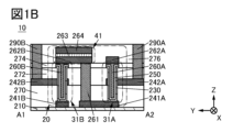
- FIG. 1B is a cross-sectional view showing a configuration example of a semiconductor device.
- FIG. 1C is a circuit diagram for explaining the configuration of the semiconductor device.
- FIG. 2 is a top view showing a configuration example of a semiconductor device.
- 3A and 3D are top views showing configuration examples of transistors.
- 3B and 3C are cross-sectional views showing configuration examples of transistors.
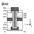
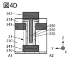
- 4A to 4D are cross-sectional views showing configuration examples of transistors.
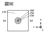
- 5A, 5D, and 5E are top views showing configuration examples of transistors.
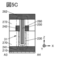
- 5B and 5C are cross-sectional views showing configuration examples of transistors.
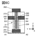
- 6A to 6C are cross-sectional views showing configuration examples of transistors.
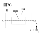
- FIG. 7A, 7C, 7E, and 7G are top views showing configuration examples of capacitors.
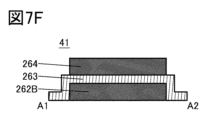
- 7B, 7D, 7F, and 7H are cross-sectional views showing configuration examples of capacitors.
- FIG. 8 is a cross-sectional view showing a configuration example of a semiconductor device.
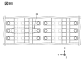
- 9A and 9B are top views showing configuration examples of the semiconductor device.
- FIG. 10A is a top view showing a configuration example of a semiconductor device.
- FIG. 10B is a cross-sectional view showing a configuration example of a semiconductor device.
- FIG. 10C is a circuit diagram for explaining the configuration of the semiconductor device.
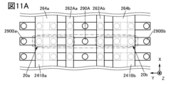
- 11A to 11C are top views showing configuration examples of semiconductor devices.
- FIG. 12A is a top view showing a configuration example of a semiconductor device.
- FIG. 12A is a top view showing a configuration example of a semiconductor device.
- FIG. 12B is a cross-sectional view showing a configuration example of a semiconductor device.
- FIG. 12C is a circuit diagram for explaining the configuration of the semiconductor device.
- FIG. 13A is a cross-sectional view showing a configuration example of a semiconductor device.
- FIG. 13B is a circuit diagram for explaining the configuration of the semiconductor device.
- 14A and 14B are cross-sectional views showing configuration examples of semiconductor devices.
- FIG. 15A is a top view showing a configuration example of a semiconductor device.
- FIG. 15B is a cross-sectional view showing a configuration example of a semiconductor device.
- FIG. 15C is a circuit diagram for explaining the configuration of the semiconductor device.
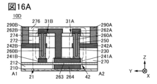
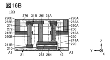
- 16A and 16B are cross-sectional views showing configuration examples of semiconductor devices.
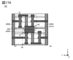
- FIG. 17A is a cross-sectional view showing a configuration example of a semiconductor device.
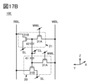
- FIG. 17B is a circuit diagram for explaining the configuration of the semiconductor device.
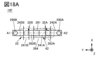
- FIG. 18A is a top view showing a configuration example of a semiconductor device.
- FIG. 18B is a cross-sectional view showing a configuration example of a semiconductor device.
- FIG. 18C is a circuit diagram for explaining the configuration of the semiconductor device.
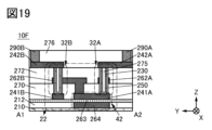
- FIG. 19 is a cross-sectional view showing a configuration example of a semiconductor device.
- 20A and 20D are top views showing configuration examples of transistors.
- 20B and 20C are cross-sectional views showing configuration examples of transistors.
- FIG. 21 is a cross-sectional view showing a configuration example of a transistor.
- FIG. 21 is a cross-sectional view showing a configuration example of a transistor.
- FIG. 22 is a cross-sectional view showing a configuration example of a semiconductor device.
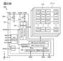
- 23A and 23B are diagrams illustrating an example of a storage device.
- FIG. 24 is a circuit diagram showing an example of a memory layer.
- FIG. 25 is a timing chart for explaining an operation example of the memory cell.
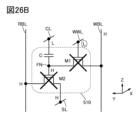
- 26A and 26B are circuit diagrams for explaining an operation example of the memory cell.
- 27A and 27B are circuit diagrams for explaining an operation example of the memory cell.
- FIG. 28 is a circuit diagram for explaining a configuration example of a semiconductor device.
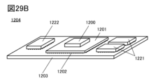
- 29A and 29B are diagrams showing an example of a semiconductor device.
- 30A and 30B are diagrams showing an example of an electronic component.
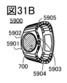
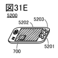
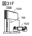
- 31A to 31J are diagrams illustrating examples of electronic devices.
- 32A to 32E are diagrams illustrating examples of electronic devices.
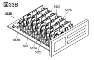
- 33A to 33C are diagrams illustrating examples of electronic devices.
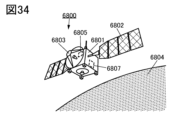
- FIG. 34 is a diagram showing an example of space equipment.
- the ordinal numbers “first” and “second” are used for convenience, and limit the number of constituent elements or the order of constituent elements (for example, the order of steps or the order of stacking). not something to do. Also, the ordinal number given to an element in one place in this specification may not match the ordinal number given to that element elsewhere in the specification or in the claims.
- film and “layer” can be interchanged depending on the case or situation.
- conductive layer can be changed to the term “conductive film.”
- insulating film can be changed to the term “insulating layer”.
- insulator can be replaced with an insulating film or an insulating layer.
- conductor can be replaced with a conductive film or a conductive layer.
- semiconductor can be interchanged with a semiconductor film or a semiconductor layer.
- oxynitride refers to a material whose composition contains more oxygen than nitrogen
- nitride oxide refers to a material whose composition contains more nitrogen than oxygen. point to the material.
- silicon oxynitride refers to a material whose composition contains more oxygen than nitrogen
- silicon nitride oxide refers to a material whose composition contains more nitrogen than oxygen. indicates
- equal in height indicates a configuration in which the height from a reference plane (for example, a flat plane such as a substrate surface) is equal in cross-sectional view.
- planarization processing typically CMP processing
- CMP processing may expose the surface of a single layer or multiple layers.
- the surfaces to be CMP-processed have the same height from the reference surface.
- the heights of the layers may differ depending on the processing apparatus, processing method, or material of the surface to be processed during CMP processing. In this specification and the like, this case is also treated as "matching heights".
- the height of the top surface of the first layer and the height of the second layer When the height difference from the upper surface of the layer is 20 nm or less, it is also said to be "matched in height".
- matching edges means that at least a part of the outline overlaps between the laminated layers when viewed from the top.
- the upper layer and the lower layer may be processed with the same mask pattern or partially with the same mask pattern.
- the outlines do not overlap, and the outline of the upper layer may be located inside the outline of the lower layer, or the outline of the upper layer may be located outside the outline of the lower layer. match.
- match includes both the case of complete match and the case of approximate match.
- One embodiment of the present invention relates to a semiconductor device provided over a substrate.
- a semiconductor device has a first transistor, a second transistor, and a capacitor, which can form a memory cell. Since a semiconductor device of one embodiment of the present invention includes memory cells, it has a function of storing data. Therefore, a semiconductor device of one embodiment of the present invention can be called a memory device.
- a semiconductor device of one embodiment of the present invention preferably includes a transistor (OS transistor) including a metal oxide in a channel formation region.
- the OS transistor has a small off current. Therefore, memory contents can be retained for a long time by using the OS transistor for a semiconductor device that can serve as a memory device.
- the refresh operation is not required or the frequency of the refresh operation is extremely low, the power consumption of the semiconductor device can be sufficiently reduced. Therefore, a semiconductor device with low power consumption can be provided.
- the OS transistor since the OS transistor has high frequency characteristics, the semiconductor device can read and write data at high speed. Therefore, a semiconductor device with high operating speed can be provided.
- the first transistor is provided in the same layer as the second transistor.
- Each of the first and second transistors has first to third conductors, a metal oxide, and an insulator.
- the second conductor is provided on the first conductor and has a region overlapping with the first conductor.
- the second conductor has an opening that overlaps with the first conductor when viewed from above.
- the metal oxide has regions in contact with the side surfaces of the opening of the second conductor and the top surface of the first conductor.
- the insulator is provided in the recess of the metal oxide.
- a third conductor is provided in the recess of the insulator.
- the third conductor has a region overlapping with the metal oxide through the insulator in a region between the first conductor and the second conductor in a cross-sectional view.
- the third conductor has a region facing the metal oxide via the insulator in a region between the first conductor and the second conductor in a cross-sectional view.
- the metal oxide has a region that functions as a channel formation region of the transistor.
- the first conductor has regions that function as one of the source and drain electrodes of the transistor.
- the second conductor has a region that functions as the other of the source and drain electrodes of the transistor.
- the third conductor has a region with a region that functions as the gate electrode of the transistor.
- the insulator has a region that functions as the gate insulator of the transistor.
- the channel length direction of the first and second transistors is the vertical direction.
- the first and second transistors are vertically structured transistors.
- a vertical transistor can be miniaturized. Therefore, by adopting a vertical structure for the first and second transistors, the transistors can be arranged at high density, and high integration in the semiconductor device can be realized.
- a transistor with a vertical structure is more likely to cause the electric field of the gate electrode to act on the entire channel formation region of the semiconductor layer. Therefore, the current density flowing through the transistor is increased, the on current of the transistor is increased, and the frequency characteristics can be improved.
- the first and second transistors when a memory cell is formed using first and second transistors, one of the first and second transistors functions as a writing transistor, and the other of the first and second transistors functions as a reading transistor. Function.
- the read transistor preferably has high on-current characteristics.
- the writing transistor preferably has low off-state current characteristics.
- the channel width related to the on-current of the transistor is adjusted by the size (also referred to as the diameter) of the opening in which a part of the component of the transistor is provided in a top view. can. Therefore, a memory device with excellent performance can be manufactured by making the opening provided with part of the components of the first transistor different from the opening provided with part of the components of the second transistor.
- FIG. 1A and 1B are a top view and a cross-sectional view, respectively, of a structure example of a semiconductor device of one embodiment of the present invention.
- FIG. 1A is a top view of the semiconductor device 10.
- FIG. 1B is a cross-sectional view of the semiconductor device 10, and is also a cross-sectional view of the portion indicated by the dashed-dotted line A1-A2 in FIG. 1A. Note that some elements are omitted in the top view of FIG. 1A for clarity of illustration.
- the semiconductor device 10 includes an insulator 210 on a substrate (not shown), a memory cell 20 on the insulator 210, a conductor 262A, a conductor 290A, a conductor 290B, and an insulator on the insulator 210. 270 , insulator 272 on insulator 270 , insulator 274 on insulator 272 , and insulator 276 on insulator 274 .
- Memory cell 20 is electrically connected to each of conductor 262A, conductor 290A, and conductor 290B.
- the memory cell 20 has a transistor 31A, a transistor 31B, a capacitor 41 on the transistor 31B, and a conductor 261. Note that the transistor 31A is provided in the same layer as the transistor 31B. Note that the components included in the semiconductor device of this embodiment may each have a single-layer structure or a laminated structure.
- the transistor 31 when describing items common to components distinguished by alphabets, reference numerals with alphabets omitted may be used.
- the transistor 31 may be referred to as a transistor 31 when describing items common to the transistor 31A and the transistor 31B.
- the direction parallel to the channel length direction of the illustrated transistor is the Z direction
- the direction perpendicular to the Z direction is the X direction
- the direction perpendicular to both the X direction and the Z direction is defined as the Y direction.
- the X direction and Y direction can be, for example, parallel to the substrate surface
- the Z direction can be perpendicular to the substrate surface.
- the transistor 31A has a conductor 241A, a conductor 242A, and a conductor 260A.
- Conductor 241A has a region that functions as one of the source and drain electrodes of transistor 31A
- conductor 242A has a region that functions as the other of the source and drain electrodes of transistor 31A
- conductor 260A has a region that functions as one of the source and drain electrodes of transistor 31A. has a region functioning as a gate electrode.
- the transistor 31B has a conductor 241B, a conductor 242B, and a conductor 260B.
- a conductor 241B has a region that functions as one of the source and drain electrodes of the transistor 31B
- a conductor 242B has a region that functions as the other of the source and drain electrodes of the transistor 31B
- a conductor 260B has a region that functions as the other of the source and drain electrodes of the transistor 31B. has a region functioning as a gate electrode.
- the capacitor 41 has a conductor 262B, an insulator 263, and a conductor 264.
- the conductor 262 B has a region that functions as one electrode of the capacitor 41
- the conductor 264 has a region that functions as the other electrode of the capacitor 41
- the insulator 263 has a region that functions as a dielectric of the capacitor 41 . have.
- the conductor 262B is electrically connected to the conductors 260B and 261, and the conductor 241A is electrically connected to the conductor 261. That is, the conductor 261 has a function of electrically connecting the conductor 262B and the conductor 241A.
- conductor 262B has a region that contacts the upper surface of each of conductors 260B and 261
- conductor 241A has a region that contacts the lower surface of conductor 261.
- the conductor 262A is electrically connected to the conductor 260A
- the conductor 290A is electrically connected to the conductor 242A
- the conductor 290B is electrically connected to the conductor 242B.
- conductor 262A has a region that contacts the top surface of conductor 260A
- conductor 290A has a region that contacts the top surface of conductor 242A
- conductor 290B has a region that contacts the top surface of conductor 242B.
- the transistor 31A is provided in the same layer as the transistor 31B. That is, the conductor 241A is provided in the same layer as the conductor 241B, and the conductor 242A is provided in the same layer as the conductor 242B. Specifically, the conductors 241 A and 241 B are provided over the insulator 210 , and the conductors 242 A and 242 B are provided over the insulator 270 .
- the conductor 262A is preferably formed from the same material and in the same process as the conductor 262B. By forming the conductor 262A using the same material and the same process as the conductor 262B, the number of steps in the manufacturing process of the semiconductor device can be reduced. At this time, conductor 262A has the same conductive material as conductor 262B. In addition, the conductor 262A is provided in the same layer as the conductor 262B. In FIG. 1B, conductor 262A and conductor 262B are provided on insulator 274. In FIG.
- FIG. 1A shows a configuration in which the conductors 241A, 242A, 242B, and 262B have the same length in the X direction.
- the present invention is not limited to this.
- the X-direction length of conductor 262B may be greater than the X-direction length of conductor 242B.
- the conductor 241B, the conductor 262A, and the conductor 264 have regions that function as wiring.
- Conductors 290A and 290B also have regions that function as plugs or wires.
- the direction in which the conductor 262A extends and the direction in which the conductor 290A extend are preferably different, and more preferably perpendicular to each other.
- the direction in which the conductor 241B extends and the direction in which the conductor 290B extends are preferably different, and more preferably perpendicular to each other.
- conductors 241B, 262A, and 264 are provided extending in the X direction.
- the direction in which the conductor 241B extends is the same as the direction in which the conductor 262A extends.
- the direction in which the conductor 241B extends is the same as the direction in which the conductor 264 extends.
- the direction in which the conductor 262A extends is the same as the direction in which the conductor 264 extends.
- the conductor 290A and the conductor 290B are provided extending in the Z direction.
- the direction in which the conductor 290A extends is the same as the direction in which the conductor 290B extends.
- the direction in which the conductor 262A extends is orthogonal to the direction in which the conductor 290A extends.
- the direction in which the conductor 241B extends is orthogonal to the direction in which the conductor 290B extends. Note that in this specification and the like, that the first direction is the same as the second direction can be rephrased as saying that the first direction is parallel to the second direction.
- FIG. 1B shows a configuration in which the conductors 290A and 290B are single layers.
- each of the conductors 290A and 290B may have a laminated structure.
- the insulators 276, 274, and 272 are used as the first conductors. It is preferable to provide the second conductor in contact with the inner wall of the provided opening, and to further provide the second conductor inside.
- the first conductor of the conductor 290A has a region that contacts the top surface of the conductor 242A, the side surface of the insulator 272, the side surface of the insulator 274, and the side surface of the insulator 276, respectively.
- the first conductor of the conductor 290B has regions in contact with the top surface of the conductor 242B, the side surfaces of the insulator 272, the side surfaces of the insulator 274, and the side surfaces of the insulator 276, respectively.
- the first conductor it is preferable to use a conductive material having a function of suppressing permeation of impurities such as water and hydrogen.
- the first conductor may have a single-layer structure or a laminated structure using one or more of tantalum, tantalum nitride, titanium, titanium nitride, ruthenium, and ruthenium oxide, for example. This can prevent water and impurities such as hydrogen from entering the metal oxide 230 through the conductors 290A and 290B.
- conductors 290A and 290B also function as wiring, conductors with high conductivity are preferably used.
- a conductive material containing tungsten, copper, or aluminum as a main component can be used for the second conductor.
- the first conductor comprises titanium and nitrogen
- the second conductor comprises tungsten
- the insulator 210 preferably functions as a barrier insulating film that prevents impurities such as water and hydrogen from diffusing from the substrate side into the transistor. Therefore, the insulator 210 has a function of suppressing the diffusion of impurities such as hydrogen atoms, hydrogen molecules, water molecules, nitrogen atoms, nitrogen molecules, nitrogen oxide molecules (N 2 O, NO, NO 2 and the like), and copper atoms. It is preferable to have an insulating material (that the impurities do not easily permeate). Alternatively, it is preferable to use an insulating material that has a function of suppressing the diffusion of oxygen (for example, at least one of oxygen atoms and oxygen molecules) (the oxygen hardly permeates).
- the insulator 210 preferably has a function of suppressing the diffusion of water, impurities such as hydrogen, and oxygen.
- silicon nitride, silicon nitride oxide, or the like can be used.
- silicon nitride which has a higher hydrogen barrier property, is preferably used as the insulator 210 .
- the insulator 210 preferably includes aluminum oxide, magnesium oxide, or the like, which has a high function of capturing and fixing hydrogen.
- water and impurities such as hydrogen can be prevented from diffusing into the transistor from the substrate side through the insulator 210 .
- diffusion of oxygen contained in the insulator 270 or the like to the substrate side can be suppressed.
- a barrier insulating film refers to an insulating film having barrier properties.
- the term "barrier property” refers to a function of suppressing diffusion of a corresponding substance (also referred to as low permeability).
- the corresponding substance has the function of capturing and fixing (also called gettering).
- the insulator 270, the insulator 272, the insulator 274, and the insulator 276 function as interlayer films.
- Insulator 270 , insulator 272 , insulator 274 , and insulator 276 each preferably have a lower dielectric constant than insulator 210 .
- the parasitic capacitance generated between wirings can be reduced.
- insulator 270, insulator 272, insulator 274, and insulator 276 may be silicon oxide, silicon oxynitride, fluorine-doped silicon oxide, carbon-doped silicon oxide, carbon- and nitrogen-doped oxide, respectively. It is preferable to include one or more of silicon and silicon oxide having vacancies.
- silicon oxide and silicon oxynitride are preferable because they are thermally stable.
- materials such as silicon oxide, silicon oxynitride, and silicon oxide having vacancies are preferable because a region containing oxygen released by heating can be easily formed.
- top surfaces of the insulators 270, 272, 274, and 276 may be planarized.
- the semiconductor device 10 can be used as a memory device.
- FIG. 1C shows a circuit diagram when the semiconductor device 10 is used as a memory device.
- the semiconductor device 10 can be rephrased as a memory device having memory cells 20 .
- the memory cell 20 has a transistor 31A, a transistor 31B, and a capacitor 41.
- FIG. 1C shows a circuit diagram when the semiconductor device 10 is used as a memory device.
- the semiconductor device 10 can be rephrased as a memory device having memory cells 20 .
- the memory cell 20 has a transistor 31A, a transistor 31B, and a capacitor 41.
- the gate electrode is electrically connected to the wiring WWL
- one of the source electrode and the drain electrode is electrically connected to one electrode of the capacitor 41
- the source electrode and the drain electrode are electrically connected to one electrode.
- the other is electrically connected to wiring WBL.
- a gate electrode is electrically connected to one electrode of the capacitor 41
- one of the source electrode and the drain electrode is electrically connected to the wiring SL
- the other of the source electrode and the drain electrode is electrically connected to the wiring RBL.
- connected to The other electrode of capacitor 41 is electrically connected to line CL.
- the wiring WWL functions as a write word line
- the wiring WBL functions as a write bit line
- the wiring RBL functions as a read bit line
- the wiring SL functions as a selection line
- the wiring CL functions as a capacitance line.
- the wiring WWL corresponds to the conductor 262A
- the wiring WBL corresponds to the conductor 290A
- the wiring RBL corresponds to the conductor 290B
- the wiring SL corresponds to the conductor 241B
- the wiring CL corresponds to the conductor 264. That is, conductor 262A has a region that functions as a write word line, conductor 290A has a region that functions as a write bit line, conductor 290B has a region that functions as a read bit line, and conductor 290B has a region that functions as a read bit line. 241B has a region that functions as a select line, and conductor 264 has a region that functions as a capacitance line.
- a memory device having memory cells will be described in detail in a later embodiment.
- FIG. 1A shows a configuration in which a straight line connecting the conductors 290A and 290B is perpendicular to the X direction.
- a straight line connecting the conductors 290A and 290B is parallel to the Y direction.
- the present invention is not limited to this.
- a straight line connecting conductors 290A and 290B may be inclined in the X direction.
- FIG. 1B can be referred to for the cross-sectional view of the portion indicated by the dashed-dotted line A1-A2 in FIG.
- FIG. 3A to 3D are top views and cross-sectional views showing configuration examples of transistors included in the memory cell 20.
- FIG. 3A is a top view of transistor 31.
- FIG. 3B is a cross-sectional view of the portion indicated by the dashed-dotted line A1-A2 in FIG. 3A
- FIG. 3C is a cross-sectional view of the portion indicated by the dashed-dotted line A3-A4 in FIG. 3A.
- FIG. 3D is a top view of the portion indicated by the dashed-dotted line B1-B2 in FIG. 3B. Note that some elements are omitted from the top views of FIGS. 3A and 3D for clarity of illustration.
- the transistor 31 includes a conductor 241 and an insulator 270 over the insulator 210, a metal oxide 230 over the conductor 241, an insulator 250 over the metal oxide 230, a conductor 260 over the insulator 250, A conductor 242 over insulator 270 and an insulator 272 over insulator 270 and conductor 242 .
- the conductor 241 has a region that functions as one of the source and drain electrodes of the transistor 31
- the conductor 242 has a region that functions as the other of the source and drain electrodes of the transistor 31
- the conductor 260 has a region that functions as the other of the source and drain electrodes of the transistor 31 .
- Metal oxide 230 has a region that functions as a channel forming region.
- a metal oxide that functions as a semiconductor (hereinafter also referred to as an oxide semiconductor) is preferably used for the metal oxide 230 .
- the bandgap of the metal oxide functioning as a semiconductor is preferably 2.0 eV or more, more preferably 2.5 eV or more.
- the off-state current of the transistor can be reduced by using a metal oxide with a large bandgap.
- metal oxide 230 it is preferable to use, for example, metal oxides such as indium oxide, gallium oxide, and zinc oxide. Moreover, as the metal oxide 230, it is preferable to use, for example, a metal oxide containing two or three elements selected from indium, the element M, and zinc.
- Element M includes gallium, aluminum, silicon, boron, yttrium, tin, copper, vanadium, beryllium, titanium, iron, nickel, germanium, zirconium, molybdenum, lanthanum, cerium, neodymium, hafnium, tantalum, tungsten, and magnesium.
- the element M is preferably one or more selected from aluminum, gallium, yttrium, and tin.
- a metal oxide containing indium, the element M, and zinc is sometimes referred to as an In-M-Zn oxide.
- the neighboring composition includes a range of ⁇ 30% of the desired atomic number ratio.
- the element M it is preferable to use gallium.
- the metal oxide 230 has a channel formation region and a source region and a drain region provided to sandwich the channel formation region in the transistor 31 . At least part of the channel formation region overlaps the conductor 260 . In other words, at least part of the channel forming region faces the conductor 260 .
- the source region overlaps one of the conductors 241 and 242 and the drain region overlaps the other of the conductors 241 and 242 . Note that the region overlapping with the conductor 242 can also be said to be a region facing the conductor 242 .
- a transistor including an oxide semiconductor when impurities and oxygen vacancies are present in a channel formation region in the oxide semiconductor, electrical characteristics are likely to fluctuate, and reliability may be degraded.
- hydrogen in the vicinity of oxygen vacancies may form defects in which hydrogen enters oxygen vacancies (hereinafter sometimes referred to as V OH ) to generate electrons serving as carriers. Therefore, if oxygen vacancies are included in the channel formation region in the oxide semiconductor, the transistor has normally-on characteristics (a channel exists even if no voltage is applied to the gate electrode, and a current flows through the transistor). easy to become. Therefore, impurities, oxygen vacancies, and VOH are preferably reduced as much as possible in the channel formation region in the oxide semiconductor.
- an insulator containing oxygen that is released by heating (hereinafter sometimes referred to as excess oxygen) is provided in the vicinity of the oxide semiconductor, and heat treatment is performed so that the oxide semiconductor is converted from the insulator.
- Oxygen can be supplied to reduce oxygen vacancies and VOH .
- the on-state current or the field-effect mobility of the transistor might be lowered.
- variations in the amount of oxygen supplied to the source region or the drain region within the substrate surface cause variations in the characteristics of the semiconductor device having transistors.
- the channel formation region is a high-resistance region with a low carrier concentration because it has less oxygen vacancies or a lower impurity concentration than the source and drain regions. Therefore, the channel forming region can be said to be i-type (intrinsic) or substantially i-type.
- the carrier concentration of the channel formation region is 1 ⁇ 10 18 cm ⁇ 3 or less, less than 1 ⁇ 10 17 cm ⁇ 3 , less than 1 ⁇ 10 16 cm ⁇ 3 , less than 1 ⁇ 10 15 cm ⁇ 3 , and 1 ⁇ 10 14 .
- cm ⁇ 3 less than 1 ⁇ 10 13 cm ⁇ 3 , less than 1 ⁇ 10 12 cm ⁇ 3 , less than 1 ⁇ 10 11 cm ⁇ 3 , or less than 1 ⁇ 10 10 cm ⁇ 3 .
- the lower limit of the carrier concentration in the channel forming region is not particularly limited, but can be, for example, 1 ⁇ 10 ⁇ 9 cm ⁇ 3 .
- the impurity concentration in the metal oxide 230 is lowered to lower the defect level density.
- a low impurity concentration and a low defect level density are referred to as high-purity intrinsic or substantially high-purity intrinsic.
- an oxide semiconductor (or metal oxide) with a low carrier concentration is sometimes referred to as a highly purified intrinsic or substantially highly purified intrinsic oxide semiconductor (or metal oxide).
- the impurities in the metal oxide 230 refer to, for example, substances other than the main components that constitute the metal oxide 230.
- an element with a concentration of less than 0.1 atomic percent can be considered an impurity.
- impurities in the metal oxide 230 include hydrogen, nitrogen, alkali metals, alkaline earth metals, iron, nickel, silicon, and the like.
- the source region and the drain region are low-resistance regions with high carrier concentration because they have many oxygen vacancies or have a high impurity concentration. That is, the source region and the drain region are n-type regions (low resistance regions) having a higher carrier concentration than the channel forming region.
- the concentrations of the metal element and the impurity element detected in each region are not limited to stepwise changes for each region, and may change continuously within each region. That is, the concentration of the impurity element may be decreased in a region closer to the channel formation region.
- Reducing the impurity concentration in the metal oxide 230 is effective in stabilizing the electrical characteristics of the transistor. Moreover, in order to reduce the impurity concentration of the metal oxide 230, it is preferable to reduce the impurity concentration in adjacent films as well.
- An opening reaching the conductor 241 is provided in the insulator 272 , the conductor 242 , and the insulator 270 .
- the opening has a region overlapping with the conductor 241 in top view.
- at least part of each of the metal oxide 230, the insulator 250, and the conductor 260 is disposed in the opening.
- the opening can be said to include the opening of the insulator 272 , the opening of the conductor 242 , and the opening of the insulator 270 .
- the conductor 242 has an opening that overlaps with the conductor 241 when viewed from above.
- the metal oxide 230 is provided in contact with the insulator 272 , the conductor 242 , and the side and bottom surfaces of the opening provided in the insulator 270 .
- the metal oxide 230 has regions in contact with the side surfaces of the opening of the conductor 242 and the top surface of the conductor 241 .
- the metal oxide 230 has a region in contact with the top surface of the insulator 272 .
- the metal oxide 230 has recesses. The recess has a region that overlaps with the opening of the conductor 242 when viewed from above.
- At least part of the insulator 250 is provided in the recess of the metal oxide 230 .
- Insulator 250 also has a region in contact with the top surface of metal oxide 230 .
- Insulator 250 also has a recess. The recess is located inside the recess of the metal oxide 230 .
- the conductor 260 is provided so as to fill the recess of the insulator 250 . Also, the conductor 260 has a region in contact with the top surface of the insulator 250 . In addition, the conductor 260 has a region overlapping with the metal oxide 230 with the insulator 250 interposed therebetween in a region between the conductor 241 and the conductor 242 in a cross-sectional view. In other words, the conductor 260 has a region facing the metal oxide 230 with the insulator 250 interposed therebetween in a region between the conductors 241 and 242 in a cross-sectional view.
- the channel length of the transistor 31 is the shortest distance (L1 in FIG. 3B) from the top surface of the conductor 241 to the bottom surface of the conductor 242 in a cross-sectional view. is also the film thickness of In other words, the channel length of the transistor 31 can be adjusted by the thickness of the insulator 270 in the region overlapping with the conductor 241 . For example, by reducing the thickness of the insulator 270, the transistor 31 with a short channel length can be manufactured.
- the channel width of the transistor 31 is the length of the region where the insulator 270 and the metal oxide 230 are in contact with each other when viewed from the top, and the length of the outline (periphery) of the metal oxide 230 when viewed from the top. be.
- the channel width of the transistor 31 can be adjusted by the diameter of the opening provided in the insulator 270 .
- the opening can be referred to as an opening in which some of the components of the transistor 31 (here, the metal oxide 230, the insulator 250, and the conductor 260) are provided.
- the transistor 31 has a structure in which a channel forming region surrounds a gate electrode. Therefore, the transistor 31 can be said to have a CAA (Channel-All-Around) structure.
- FIG. 3D shows a configuration in which the top surface shape of the opening of the conductor 242 has a circular shape
- the present invention is not limited to this.
- the top surface shape of the opening of the conductor 242 may be elliptical, polygonal, or polygonal with rounded corners.
- polygonal shapes refer to triangles, quadrilaterals, pentagons, hexagons, and the like.
- An insulator 274 is provided over the insulator 272 , and a conductor 262 is provided over the insulator 274 and the conductor 260 .
- a crystalline oxide semiconductor is preferably used for the metal oxide 230 .
- crystalline oxide semiconductors include a CAAC-OS (c-axis aligned crystalline oxide semiconductor), an nc-OS (nanocrystalline oxide semiconductor), a polycrystalline oxide semiconductor, a single-crystalline oxide semiconductor, and the like.
- CAAC-OS or nc-OS is preferably used as the metal oxide 230, and CAAC-OS is particularly preferably used.
- CAAC-OS is a metal oxide that has a dense structure with high crystallinity and few impurities and defects (for example, oxygen vacancies).
- heat treatment is performed at a temperature at which the metal oxide is not polycrystallized (for example, 400° C. or more and 600° C. or less), so that the CAAC-OS has a dense structure with higher crystallinity.
- a temperature at which the metal oxide is not polycrystallized for example, 400° C. or more and 600° C. or less
- the metal oxide 230 by using a crystalline oxide such as CAAC-OS as the metal oxide 230 , extraction of oxygen from the metal oxide 230 by the conductors 241 and 242 can be suppressed. As a result, oxygen can be suppressed from being extracted from the metal oxide 230 even when heat treatment is performed, so the transistor is stable against high temperatures (so-called thermal budget) in the manufacturing process. Further, a decrease in the conductivity of the conductors 241 and 242 can be suppressed.
- a crystalline oxide such as CAAC-OS
- the nc-OS has periodicity in the atomic arrangement in a minute region (for example, a region of 1 nm or more and 10 nm or less, particularly a region of 1 nm or more and 3 nm or less).
- the nc-OS has minute crystals (also referred to as nanocrystals).
- the nc-OS since there is no regularity in crystal orientation between different nanocrystals, no orientation is observed in the entire film. That is, when the nc-OS is used as the metal oxide 230, the film characteristics of the metal oxide 230 are constant regardless of the direction of carriers flowing through the metal oxide 230, and thus the electrical characteristics of the transistor are stable.
- the metal oxide 230 is CAAC-OS, nc-OS, pseudo-amorphous oxide semiconductor (a-like OS), amorphous oxide semiconductor, polycrystalline oxide semiconductor, CAC-OS (cloud-aligned composite oxide semiconductor) may have two or more kinds.
- the position of the peak indicating the c-axis orientation may vary depending on the type and composition of the metal elements forming the CAAC-OS.
- a plurality of bright points (spots) are observed in the electron beam diffraction pattern of the CAAC-OS film. A certain spot and another spot are observed at point-symmetrical positions with respect to the spot of the incident electron beam that has passed through the sample (also referred to as a direct spot) as the center of symmetry.
- an electron beam diffraction pattern is obtained in which a plurality of spots are observed within a ring-shaped area centered on the spot.
- the metal oxide 230 can be rephrased as a semiconductor layer including the channel formation region of the transistor 31 .
- a material that can be used for the semiconductor layer is not limited to a metal oxide that functions as a semiconductor (an oxide semiconductor).
- a semiconductor such as single crystal silicon, polycrystalline silicon, or amorphous silicon may be used as the semiconductor layer, and for example, low temperature poly silicon (LTPS) may be used.
- LTPS low temperature poly silicon
- a transition metal chalcogenide that functions as a semiconductor may be used as the semiconductor layer.
- MoTe 2 tungsten sulfide
- tungsten selenide typically WSe 2
- tungsten tellurium typically WTe 2
- hafnium sulfide typically HfS 2
- hafnium selenide typically HfSe 2
- zirconium sulfide typically ZrS 2
- zirconium selenide typically ZrSe 2
- ZrSe 2 zirconium selenide
- the insulator 250 may have a single-layer structure or a laminated structure.
- the insulator 250 for example, silicon oxide, silicon oxynitride, silicon oxide to which fluorine is added, silicon oxide to which carbon is added, silicon oxide to which carbon and nitrogen are added, silicon oxide having vacancies, or the like can be used.
- silicon oxide and silicon oxynitride are preferable because they are stable against heat.
- the insulator 250 contains at least oxygen and silicon.
- the concentration of impurities such as water and hydrogen in the insulator 250 is preferably reduced.
- an insulator having a barrier property against oxygen may be provided between the insulator 250 and the metal oxide 230 .
- the insulator is provided in contact with the lower surface of the insulator 250 and the concave portion of the metal oxide 230 . Since the insulator has a barrier property against oxygen, oxygen contained in the insulator 250 can be supplied to the channel formation region, and excessive supply of oxygen contained in the insulator 250 to the channel formation region can be suppressed. Therefore, when heat treatment or the like is performed, desorption of oxygen from the metal oxide 230 can be suppressed, and formation of oxygen vacancies in the metal oxide 230 can be suppressed. Therefore, the electrical characteristics of the transistor 31 can be improved, and the reliability can be improved.
- An insulator containing oxides of one or both of aluminum and hafnium is preferably used as the insulator.
- the insulator aluminum oxide, hafnium oxide, an oxide containing aluminum and hafnium (hafnium aluminate), an oxide containing hafnium and silicon (hafnium silicate), or the like can be used. It is more preferable to use aluminum oxide as the insulator.
- the insulator contains at least oxygen and aluminum. Note that the insulator should be less permeable to oxygen than the insulator 250, for example.
- a material that is less permeable to oxygen than the insulator 250 may be used, for example.
- magnesium oxide, gallium oxide, gallium zinc oxide, indium gallium zinc oxide, or the like may be used as the insulator.
- FIG. 3B shows a configuration in which the conductor 260 is a single layer.
- the conductor 260 may have a laminated structure.
- conductor 260 preferably has a first conductor and a second conductor over the first conductor.
- the first conductor of conductor 260 is preferably arranged to wrap the bottom and side surfaces of the second conductor of conductor 260 .
- a conductive material having a function of suppressing diffusion of impurities such as hydrogen atoms, hydrogen molecules, water molecules, nitrogen atoms, nitrogen molecules, nitrogen oxide molecules, or copper atoms is used.
- impurities such as hydrogen atoms, hydrogen molecules, water molecules, nitrogen atoms, nitrogen molecules, nitrogen oxide molecules, or copper atoms is preferred.
- a conductive material having a function of suppressing diffusion of oxygen eg, at least one of oxygen atoms and oxygen molecules
- the second conductor of the conductor 260 is oxidized by oxygen contained in the insulator 250, for example, and the conductivity is lowered. can be suppressed.
- the conductive material having a function of suppressing diffusion of oxygen titanium, titanium nitride, tantalum, tantalum nitride, ruthenium, ruthenium oxide, or the like is preferably used, for example.
- the conductor 260 use a conductor with high conductivity.
- the second conductor of conductor 260 can use a conductive material whose main component is tungsten, copper, or aluminum.
- the second conductor of the conductor 260 may have a layered structure, for example, a layered structure of titanium or titanium nitride and any of the above conductive materials.
- an insulator having a barrier property against hydrogen may be provided between the insulator 250 and the conductor 260 .
- impurities such as hydrogen contained in the conductor 260 can be prevented from diffusing into the insulator 250 and the metal oxide 230 .
- Silicon nitride for example, may be used as the insulator.
- the insulator contains at least nitrogen and silicon.
- aluminum oxide, magnesium oxide, hafnium oxide, gallium oxide, indium gallium zinc oxide, silicon nitride oxide, or the like may be used.
- the insulator may be less permeable to hydrogen than the insulator 250, for example.
- a material that is less permeable to hydrogen than the insulator 250 may be used, for example.
- An insulator having a barrier property against oxygen may be provided between the insulator 250 and the conductor 260 .
- diffusion of oxygen contained in the insulator 250 to the conductor 260 can be suppressed.
- reduction in the amount of oxygen supplied to the metal oxide 230 can be suppressed.
- oxidation of the conductor 260 due to oxygen contained in the insulator 250 can be suppressed.
- An insulator containing oxides of one or both of aluminum and hafnium is preferably used as the insulator.
- the insulator aluminum oxide, hafnium oxide, an oxide containing aluminum and hafnium (hafnium aluminate), an oxide containing hafnium and silicon (hafnium silicate), or the like can be used.
- Hafnium oxide is more preferably used as the insulator.
- the insulator contains at least oxygen and hafnium.
- Hafnium oxide is suitable because it has a barrier property against hydrogen.
- Metal oxide 230, insulator 250, and conductor 260 are formed in insulator 272, conductor 242, and openings provided in insulator 270 by atomic layer deposition (ALD).
- ALD atomic layer deposition
- the ALD method includes a thermal ALD (thermal ALD) method in which reaction of a precursor and a reactant is performed only with thermal energy, a PEALD (plasma enhanced ALD) method using a plasma-excited reactant, and the like.
- PEALD plasma enhanced ALD
- film formation can be performed at a lower temperature by using plasma, which is preferable in some cases.
- the ALD method can deposit atoms one layer at a time, it is possible to deposit ultra-thin films, to form films with high aspect ratio structures, to form films with few defects such as pinholes, and to improve coverage. It has effects such as enabling excellent film formation and enabling film formation at a low temperature. Therefore, the metal oxide 230, the insulator 250, and the conductor 260 can be deposited on the side surfaces of the openings provided in the insulator 272, the conductor 242, and the insulator 270 with good coverage.
- a film formed by the ALD method may contain more impurities such as carbon than films formed by other film forming methods.
- quantification of impurities can be performed using secondary ion mass spectrometry (SIMS: Secondary Ion Mass Spectrometry), X-ray photoelectron spectroscopy (XPS: X-ray Photoelectron Spectroscopy), or Auger electron spectroscopy (AES: Auger Electron Spectroscopy) can be performed using
- microwave treatment after forming a metal oxide film using the ALD method, and it is more preferable to perform microwave treatment in an atmosphere containing oxygen.
- oxygen gas By performing microwave treatment in an oxygen-containing atmosphere, oxygen gas can be plasmatized using high frequencies such as microwaves and RF, and the oxygen plasma can act on metal oxides. At this time, it is also possible to irradiate the metal oxide with high frequency waves such as microwaves and RF. That is, the metal oxide can be acted on by microwaves, high frequencies such as RF, oxygen plasma, and the like.
- the impurity concentration of the metal oxide can be reduced by the action of high frequency, oxygen plasma, or the like.
- hydrogen in the metal oxide can be released as water molecules.
- carbon in the metal oxide can be desorbed as oxocarbon (CO and/or CO 2 ).
- oxygen vacancies, VOH , and the like in the metal oxide can be reduced by supplying oxygen radicals generated by oxygen plasma to the metal oxide.
- the atoms in the metal oxide are given energy higher than the processing temperature of the microwave treatment. Therefore, the rearrangement of the metal atoms and oxygen atoms in the metal oxide is promoted, and the crystallinity of the metal oxide can be improved. Note that the crystallinity of the metal oxide tends to improve as the impurity concentration and the amount of defects (oxygen vacancies, VOH , etc.) in the metal oxide are reduced. In other words, microwave treatment in an oxygen-containing atmosphere reduces the impurity concentration and the amount of defects in the metal oxide and improves the crystallinity of the metal oxide.
- the insulator 270 is, for example, an oxide containing silicon such as silicon oxide, silicon oxynitride, fluorine-added silicon oxide, carbon-added silicon oxide, carbon- and nitrogen-added silicon oxide, or silicon oxide having vacancies. is preferably used.
- silicon oxide and silicon oxynitride are preferable because they are thermally stable.
- a material such as silicon oxide, silicon oxynitride, or silicon oxide having vacancies is preferable because a region containing excess oxygen can be easily formed.
- the metal oxide 230 in the region in contact with the insulator 270 functions as a channel formation region; or substantially i-type.
- insulator 270 preferably comprises silicon oxide or an oxide containing silicon, such as silicon oxynitride.
- the conductors 241 and 242 it is preferable to use a conductive material that is difficult to oxidize or a conductive material that has a function of suppressing the diffusion of oxygen.
- the conductive material include a conductive material containing nitrogen and a conductive material containing oxygen. By using the conductive material, a decrease in the conductivity of the conductors 241 and 242 can be suppressed.
- each of the conductors 241 and 242 contains at least metal and nitrogen.
- nitrides containing tantalum for example, nitrides containing titanium, nitrides containing molybdenum, nitrides containing tungsten, nitrides containing tantalum and aluminum, titanium, and aluminum are used, respectively. It is preferable to use a nitride or the like containing In one aspect of the present invention, nitrides containing tantalum are particularly preferred.
- ruthenium oxide, ruthenium nitride, an oxide containing strontium and ruthenium, an oxide containing lanthanum and nickel, or the like may be used. These materials are preferable because they are conductive materials that are difficult to oxidize or materials that maintain conductivity even after absorbing oxygen.
- FIG. 3B shows a configuration in which the conductors 241 and 242 are single layers.
- each of the conductors 241 and 242 may have a laminated structure.
- each of the conductors 241 and 242 may have a two-layer structure of a first conductor and a second conductor.
- a conductive material that is difficult to oxidize or a conductive material that has a function of suppressing diffusion of oxygen is preferably used as the first conductor in contact with the insulator 270. Accordingly, a decrease in the conductivity of the conductors 241 and 242 can be suppressed.
- the second conductors of the conductors 241 and 242 preferably have higher conductivity than the first conductors of the conductors 241 and 242 . Further, it is preferable that the thickness of the second conductors of the conductors 241 and 242 be larger than the thickness of the first conductors of the conductors 241 and 242 .
- tantalum nitride or titanium nitride can be used as the first conductors of the conductors 241 and 242, and tungsten can be used as the second conductors of the conductors 241 and 242.
- an insulator having a barrier property against oxygen is preferably provided between the conductor 241 and the insulator 270 in order to suppress oxidation of the conductor 241 by oxygen contained in the insulator 270 .
- an insulator having a barrier property against oxygen is preferably provided between the conductor 242 and the insulator 270 in order to suppress oxidation of the conductor 242 due to oxygen contained in the insulator 270 .
- An insulator containing an oxide of one or both of aluminum and hafnium is preferably used as the insulator.
- aluminum oxide, hafnium oxide, an oxide containing aluminum and hafnium (hafnium aluminate), an oxide containing hafnium and silicon (hafnium silicate), or the like can be used.
- the ends of the conductor 260 coincide with the respective ends of the metal oxide 230 and the insulator 250, as shown in FIG. 3B.
- the edges of the conductor 260 may not be aligned with the edges of the metal oxide 230 and the insulator 250 .
- a portion of conductor 260 is removed.
- the end of conductor 260 coincides with the end of conductor 262 .
- FIG. 3B shows a configuration in which the conductor 241 does not have a recess in the region overlapping the opening of the insulator 270 .
- the conductor 241 may have recesses in regions overlapping the openings. In other words, a portion of the upper surface of the conductor 241 overlapping the opening may be removed. Since the conductor 241 has a recess in a region overlapping with the opening, the end of the region (the facing region) where the metal oxide 230 and the conductor 260 overlap with the insulator 250 interposed therebetween can be brought closer to the conductor 241. can be done.
- the conductor 260 can have a region that overlaps (faces with) the conductor 241 with the metal oxide 230 and the insulator 250 interposed therebetween.
- a region where the metal oxide 230 and the conductor 260 do not overlap with each other with the insulator 250 interposed therebetween (region where they do not face each other), that is, a so-called Loff region is narrowed or provided. can be configured without Therefore, the frequency characteristic of transistor 31 can be improved.
- the write speed and read speed of the memory cell 20 can be improved, and the operating speed of the semiconductor device 10 can be improved. Therefore, a semiconductor device with high operating speed can be provided.
- the conductor 241 may have an opening that overlaps with the opening of the insulator 270 and reaches the insulator 210 .
- a region of the conductor 241 that overlaps the opening of the insulator 270 may be removed. Since the conductor 241 has an opening that reaches the insulator 210 , an end portion of a region where the metal oxide 230 and the conductor 260 overlap (face each other) with the insulator 250 interposed therebetween can be brought closer to the conductor 241 . can.
- the conductor 260 can have a region that overlaps (faces with) the conductor 241 with the metal oxide 230 and the insulator 250 interposed therebetween. Therefore, the frequency characteristic of transistor 31 can be improved.
- FIG. 3B shows a configuration in which the metal oxide 230 has a region in contact with the top surface of the insulator 272 .
- the present invention is not limited to this.
- insulator 272 may not be provided, as shown in FIG. 4D.
- the metal oxide 230 has regions in contact with part of the top surface of the conductor 242 and the side surfaces of the opening of the conductor 242 .
- the contact area between the metal oxide 230 and the conductor 242 can be increased, and the on-state current of the transistor 31 can be increased. Therefore, a semiconductor device with large on-current can be provided.
- FIGS. 5A-5E show a transistor having a different configuration than the transistor 31 shown in FIGS. 3A-3D.
- FIGS. 5A to 5E are top views and cross-sectional views showing another configuration example of the transistor 31.
- FIG. 5A, 5D, and 5E are top views of transistor 31.
- FIG. 5B is a cross-sectional view of the portion indicated by the dashed-dotted line A1-A2 in FIG. 5A
- FIG. 5C is a cross-sectional view of the portion indicated by the dashed-dotted line A3-A4 in FIG. 5A
- 5D is a top view of the portion indicated by the dashed-dotted line B1-B2 in FIG. 5B
- FIG. 5E is a top view of the portion indicated by the dashed-dotted line B3-B4 in FIG. 5B.
- some elements are omitted for clarity of illustration.
- a transistor 31 shown in FIGS. 5A to 5E is a modification of the transistor 31 shown in FIGS. 3A to 3D.
- the transistor 31 shown in FIGS. 5A-5E differs from the transistor 31 shown in FIGS. 3A-3D in the shape of the metal oxide 230, the insulator 250, and the conductor 260.
- FIG. hereinafter, portions different from the transistor 31 shown in FIGS. 3A to 3D will mainly be described, and descriptions of overlapping portions will be omitted.
- the diameters of the openings of the insulator 272 and the conductor 242 are smaller than the diameter of the opening of the insulator 270 .
- the metal oxide 230 is provided in contact with the side and bottom surfaces of the opening of the insulator 270 . At this time, the top surface of the metal oxide 230 has a region that matches the top surface of the insulator 270 and contacts the bottom surface of the conductor 242 .
- the insulator 250 is provided in openings of the insulator 272 and the conductor 242 and in recesses of the metal oxide 230 .
- the insulator 250 has regions in contact with the side surfaces of the opening of the insulator 272 and the side surfaces of the opening of the conductor 242 .
- the top surface of insulator 250 coincides with the respective top surfaces of conductor 260 and insulator 272 .
- the conductor 260 is provided so as to fill the recess of the insulator 250 .
- Conductor 260 has a region that contacts the lower surface of conductor 262 .
- the structure shown in FIGS. 5A to 5E forms the metal oxide 230 in the opening of the insulator 270, and the insulating material is formed in the opening of the insulator 272, the opening of the conductor 242, and the recess of the metal oxide 230.
- An insulating film to be the body 250 and a conductive film to be the conductor 260 are formed, and planarization is performed until the top surface of the insulator 272 is exposed.
- CMP chemical mechanical polishing
- the metal oxide 230 is provided below the insulator 272 and therefore does not come into contact with the conductor 262 on the insulator 272 . Therefore, the metal oxide 230 can function as a channel formation region of the transistor 31 . Further, compared with the transistor 31 shown in FIGS. 3A to 3D, the transistor 31 shown in FIGS. 5A to 5E can form the insulator 250 and the conductor 260 without using a photolithography method. Therefore, it is possible to achieve a reduction in size or a high degree of integration. In addition, since the insulator 274 is not required, the number of steps in manufacturing the semiconductor device can be reduced.
- FIG. 5B shows a configuration in which the conductor 241 does not have a recess in the region overlapping the opening of the insulator 270 .
- the present invention is not limited to this.
- the conductor 241 may have recesses in regions overlapping the openings. In other words, a portion of the upper surface of the conductor 241 overlapping the opening may be removed.
- conductor 241 may have an opening that overlaps the opening and reaches insulator 210 . In other words, a region of the conductor 241 that overlaps the opening of the insulator 270 may be removed.
- the conductor 241 has a recessed portion or an opening in a region overlapping with the opening of the insulator 270, so that the end portion of the region (the facing region) where the metal oxide 230 and the conductor 260 overlap with the insulator 250 interposed therebetween. , can be brought closer to the conductor 241 . Therefore, the frequency characteristic of transistor 31 can be improved.
- FIG. 5B shows a configuration in which the metal oxide 230 has recesses.
- metal oxide 230 may have openings down to conductors 241, as shown in FIG. 6C.
- the metal oxide 230 may have a hollow cylindrical shape.
- the conductor 241 has a recessed portion or an opening in a region overlapping with the opening of the insulator 270, as in FIGS. 6A and 6B. good too.
- the contact area between the conductor 241 and the metal oxide 230 can be increased, and the on-state current of the transistor 31 can be increased.
- FIG. 7A and 7B are a top view and a cross-sectional view showing a configuration example of the capacitor 41 of the memory cell 20.
- FIG. 7A is a top view of the capacitor 41.
- FIG. 7B is a cross-sectional view of the portion indicated by the dashed-dotted line A1-A2 in FIG. 7A. Note that some elements are omitted in the top view of FIG. 7A for clarity of illustration.
- the capacitor 41 has a conductor 262B, an insulator 263 on the conductor 262B, and a conductor 264 on the insulator 263.
- the conductor 262 B has a region that functions as one electrode of the capacitor 41
- the conductor 264 has a region that functions as the other electrode of the capacitor 41
- the insulator 263 has a region that functions as a dielectric of the capacitor 41 .
- the capacitor 41 constitutes an MIM (Metal-Insulator-Metal) capacitor.
- the conductor 264 is provided extending outside the end of the conductor 262B in the X direction. 7A and 7B, the Y-direction end of the conductor 262B coincides with the Y-direction end of the insulator 263 and the conductor 264, respectively.
- the conductor 262B and the conductor 264 may each have a single-layer structure or a laminated structure.
- Each of conductor 262B and conductor 264 may have a first conductor and a second conductor on the first conductor. Note that one or both of the conductor 262B and the conductor 264 may be stacked in the opposite order.
- a conductor that can be used as the first conductors of the conductors 241 and 242 may be used as the first conductors of the conductors 262B and 264 .
- a conductor that can be used as the second conductors of the conductors 241 and 242 may be used.
- titanium nitride can be used as the first conductor of the conductor 262B and the conductor 264
- tungsten can be used as the second conductor of the conductor 262B and the conductor 264.
- a high dielectric constant (high-k) material (high dielectric constant material) is preferably used for the insulator 263 .
- the insulator 263 is preferably formed by a film formation method with good coverage, such as an ALD method or a CVD method.
- high dielectric constant (high-k) materials examples include oxides, oxynitrides, nitride oxides, and nitrides containing one or more metal elements selected from aluminum, hafnium, zirconium, gallium, and the like. be done.
- silicon may be contained in the above oxide, oxynitride, nitride oxide, or nitride. Insulators made of the above materials can also be laminated and used.
- high dielectric constant (high-k) materials include aluminum oxide, hafnium oxide, zirconium oxide, oxides containing aluminum and hafnium, oxynitrides containing aluminum and hafnium, oxides containing silicon and hafnium, Oxynitrides with silicon and hafnium, oxides with silicon and zirconium, oxynitrides with silicon and zirconium, oxides with hafnium and zirconium, and oxynitrides with hafnium and zirconium.
- the insulator 263 can be thick enough to suppress leakage current and the capacitance of the capacitor 41 can be sufficiently secured.
- a laminated insulator composed of the above materials, and a laminated structure of a high dielectric constant (high-k) material and a material having a higher dielectric strength than the high dielectric constant (high-k) material is used.
- high-k high dielectric constant
- high-k high dielectric constant
- an insulator in which zirconium oxide, aluminum oxide, and zirconium oxide are stacked in this order can be used as the insulator 263 .
- an insulator in which zirconium oxide, aluminum oxide, zirconium oxide, and aluminum oxide are stacked in this order can be used.
- an insulating film in which hafnium zirconium oxide, aluminum oxide, hafnium zirconium oxide, and aluminum oxide are stacked in this order can be used.
- an insulator having a relatively high dielectric strength, such as aluminum oxide the dielectric strength is improved and electrostatic breakdown of the capacitor 41 can be suppressed.
- 7A and 7B show a configuration in which the Y-direction end of the conductor 262B matches the Y-direction end of the insulator 263 and the conductor 264, respectively.
- the present invention is not limited to this.
- FIGS. 7C and 7D are a top view and a cross-sectional view showing another configuration example of the capacitor 41.
- FIG. 7C is a top view of capacitor 41.
- FIG. FIG. 7D is a cross-sectional view of the portion indicated by the dashed-dotted line A1-A2 in FIG. 7C.
- the Y-direction end of the conductor 262B may be located outside the Y-direction ends of the conductor 264 and the insulator 263, respectively.
- FIG. 7D shows a configuration in which the end of the conductor 264 in the Y direction coincides with the end of the insulator 263 in the Y direction, but the present invention is not limited to this.
- the Y-direction end of the conductor 264 may be located inside the Y-direction end of the insulator 263 .
- FIG. 7E and 7F are a top view and a cross-sectional view showing another configuration example of the capacitor 41.
- FIG. 7E is a top view of capacitor 41.
- FIG. FIG. 7F is a cross-sectional view of the portion indicated by the dashed-dotted line A1-A2 in FIG. 7E.
- the insulator 263 may be provided to cover the top and side surfaces of the conductor 262B.
- FIG. 7F shows a configuration in which the insulator 263 is in contact with the side and top surfaces of the conductor 262B. With this structure, the insulator 263 can sufficiently separate the conductor 264 and the conductor 262B.
- FIG. 7F shows a configuration in which the Y-direction end of the conductor 264 coincides with the Y-direction end of the conductor 262B.
- the present invention is not limited to this.
- FIG. 7G and 7H are a top view and a cross-sectional view showing another configuration example of the capacitor 41.
- FIG. 7G is a top view of capacitor 41.
- FIG. FIG. 7H is a cross-sectional view of the portion indicated by the dashed-dotted line A1-A2 in FIG. 7G.
- the Y-direction end of the conductor 264 may be located outside the Y-direction end of the conductor 262B.
- the outer circumference of the conductor 262B is located inside the outer circumference of the conductor 264 in top view.
- the Y-direction end of the conductor 264 may be located inside the Y-direction end of the conductor 262B.
- FIG. 1B shows a configuration in which the capacitor 41 has a planar shape. In other words, a configuration in which the capacitor 41 is provided on the insulator 274 is shown.
- the present invention is not limited to this.
- FIG. 8 shows a cross-sectional view of a semiconductor device different from the semiconductor device 10 shown in FIG. 1B. Note that FIG. 1A can be referred to for the top view of the semiconductor device illustrated in FIG.
- the semiconductor device shown in FIG. 8 differs from the semiconductor device 10 shown in FIG. 1B in the configuration and shape of the capacitor 41 .
- the semiconductor device shown in FIG. 8 also differs from the semiconductor device 10 shown in FIG. 1B in that it does not have the conductor 262B.
- a portion of the capacitor 41 may be positioned within openings provided in the insulators 274, 272, and 270.
- the capacitor 41 has a conductor 261 , an insulator 263 over the conductor 261 , and a conductor 264 over the insulator 263 .
- the conductor 261 has a region in contact with the side and bottom surfaces of the opening, a region in contact with the top surface of the conductor 260B, and a region in contact with part of the top surface of the insulator 274 .
- the conductor 264 has a region embedded in the opening with the conductor 261 and the insulator 263 interposed therebetween. With this structure, the capacitance per unit area of the capacitor 41 can be increased.
- the semiconductor device 10 can be used as a memory device having the memory cells 20.
- a memory cell array can be configured by arranging the memory cells 20 in a matrix.
- FIG. 9A shows a memory cell array in which a plurality of memory cells 20 are arranged in the X direction.
- FIG. 9A is a top view of a memory cell array.
- the memory cell array shown in FIG. 9A has a plurality of memory cells 20 arranged in the X direction. Note that FIG. 9A shows a region including three memory cells 20 .
- the conductor 241B, the conductor 262A, and the conductor 264 are provided extending in the X direction. At this time, each of the conductors 241 B, 262 A, and 264 is shared by the plurality of memory cells 20 . With such a structure, miniaturization or high integration of the semiconductor device can be achieved.
- FIG. 9B is a top view of a memory cell array in which a plurality of memory cells 20 are arranged in each of the X direction and the Y direction. Note that FIG. 9B shows a region including six memory cells 20 .
- ⁇ Modification 1 of semiconductor device> An example of a semiconductor device that is different from the semiconductor device shown in ⁇ Structure Example 1 of Semiconductor Device> is described below.
- structures having the same functions as the structures constituting the semiconductor device described in ⁇ Structure Example 1 of Semiconductor Device> are denoted by the same reference numerals.
- portions different from those of the semiconductor device shown in ⁇ Structure Example 1 of Semiconductor Device> will be mainly described, and descriptions of overlapping portions will be omitted.
- FIG. 10A and 10B are a top view and a cross-sectional view, respectively, showing a configuration example of the semiconductor device 10A.
- FIG. 10A is a top view of the semiconductor device 10A.
- FIG. 10B is a cross-sectional view of the portion indicated by the dashed-dotted line A1-A2 in FIG. 10A. Note that some elements are omitted in the top view of FIG. 10A for clarity of illustration.
- the semiconductor device 10A has a memory cell 20a, a memory cell 20b, a conductor 262Aa, a conductor 262Ab, a conductor 290A, a conductor 290Ba, and a conductor 290Bb. Moreover, the memory cell 20a is provided in the same layer as the memory cell 20b.
- the memory cell 20a has a transistor 31Aa, a transistor 31Ba, a capacitor 41a, and a conductor 261a.
- the transistor 31Aa has a conductor 241Aa, a conductor 242A, and a conductor 260Aa.
- the transistor 31Ba has a conductor 241Ba, a conductor 242Ba, and a conductor 260Ba.
- the capacitor 41a has a conductor 262Ba, an insulator 263a, and a conductor 264a.
- the memory cell 20b has a transistor 31Ab, a transistor 31Bb, a capacitor 41b, and a conductor 261b.
- the transistor 31Ab has a conductor 241Ab, a conductor 242A, and a conductor 260Ab.
- the transistor 31Bb includes a conductor 241Bb, a conductor 242Bb, and a conductor 260Bb.
- the capacitor 41b has a conductor 262Bb, an insulator 263b, and a conductor 264b.
- the conductor 290A is electrically connected to the conductor 242A.
- the semiconductor device 10A has a symmetrical configuration with the one-dot chain line of C1-C2 as the axis of symmetry.
- the memory cell 20b is arranged at a line-symmetrical position with respect to the memory cell 20a with the conductor 290A as the axis of symmetry. Therefore, the memory cell 20a and the memory cell 20b can be collectively called a pair of memory cells.
- the conductor 242A has a region functioning as the other of the source and drain electrodes of the transistor 31Aa and a region functioning as the other of the source and drain electrodes of the transistor 31Ab.
- the semiconductor device 10A can be used as a memory device.
- FIG. 10C shows a circuit diagram when the semiconductor device 10A is used as a memory device.
- the semiconductor device 10A can be rephrased as a memory device having memory cells 20a and 20b.
- the memory cell 20a has a transistor 31Aa, a transistor 31Ba, and a capacitor 41a.
- the memory cell 20b has a transistor 31Ab, a transistor 31Bb, and a capacitor 41b.
- a gate electrode is electrically connected to the wiring WWLa
- one of the source electrode and the drain electrode is electrically connected to one electrode of the capacitor 41a
- the other of the source electrode and the drain electrode is electrically connected to the wiring WBL.
- the gate electrode is electrically connected to one electrode of the capacitor 41a
- one of the source and drain electrodes is electrically connected to the wiring SLa
- the other of the source and drain electrodes is electrically connected to the wiring RBLa.
- the other electrode of the capacitor 41a is connected to the wiring CLa.
- a gate electrode is electrically connected to the wiring WWLb, one of the source electrode and the drain electrode is electrically connected to one electrode of the capacitor 41b, and the other of the source electrode and the drain electrode is electrically connected to the wiring WBL.
- the gate electrode is electrically connected to one electrode of the capacitor 41b, one of the source and drain electrodes is electrically connected to the wiring SLb, and the other of the source and drain electrodes is electrically connected to the wiring RBLb. connected to The other electrode of capacitor 41b is connected to line CLb.
- the wiring WWLa corresponds to the conductor 262Aa
- the wiring WBL corresponds to the conductor 290A
- the wiring SLa corresponds to the conductor 241Ba
- the wiring RBLa corresponds to the conductor 290Ba
- the wiring CLa corresponds to the conductor 264a.
- the wiring WWLb corresponds to the conductor 262Ab
- the wiring SLb corresponds to the conductor 241Bb
- the wiring RBLb corresponds to the conductor 290Bb
- the wiring CLb corresponds to the conductor 264b.
- the wiring WBL is shared by the memory cell 20a and the memory cell 20b. That is, the write bit line is shared by the memory cells 20a and 20b.
- the conductor 290A functions as a write bit line for the memory cell 20a and as a write bit line for the memory cell 20b.
- connection between the memory cell 20a, the memory cell 20b, and the wiring is configured as described above, so that a semiconductor device that can be miniaturized or highly integrated can be provided.
- the semiconductor device 10A can be used as a storage device having a pair of memory cells.
- a memory cell array can be configured by arranging a pair of memory cells in a matrix.
- FIG. 11A shows an example of a memory cell array in which a plurality of pairs of memory cells are arranged in the X direction. Note that FIG. 11A shows a region including three pairs of memory cells.
- FIG. 11A a pair of memory cells is configured by the memory cell 20a and the memory cell 20b included in the area surrounded by the two-dot chain line.
- FIG. 11A shows a structure in which a conductor 290Ba, a conductor 290A, and a conductor 290Bb are arranged on the same straight line in a pair of memory cells.
- a straight line connecting conductors 290Ba, 290A, and 290Bb is parallel to the Y direction. That is, in a pair of memory cells, a straight line connecting the conductors 290Ba, 290A, and 290Bb is perpendicular to the X direction.
- the present invention is not limited to this.
- FIG. 11B is a top view showing another example of a memory cell array. Note that FIG. 10B can be referred to for the cross-sectional view of the portion indicated by the dashed-dotted line A1-A2 in FIG. 11B.
- a pair of memory cells is configured by the memory cell 20a and the memory cell 20b included in the area surrounded by the two-dot chain line. Also, similar to the pair of memory cells shown in FIG. 11A, conductor 290A is shared between memory cell 20a and memory cell 20b.
- a straight line connecting conductors 290A and 290Ba electrically connected to the memory cell 20a is inclined in the X direction. Note that the conductor 262Aa, the conductor 264a, and the conductor 241Ba are provided extending in the X direction. not orthogonal.
- a straight line connecting conductors 290A and 290Bb electrically connected to the memory cell 20b is inclined in the X direction.
- the conductor 262Ab, the conductor 264b, and the conductor 241Bb are provided extending in the X direction, so that the straight line corresponds to the direction in which the conductor 262Ab, the conductor 264b, and the conductor 241Bb extend. not orthogonal.
- the memory density of the memory cell array may be increased.
- the pair of memory cells has a symmetrical configuration with the dashed-dotted line A3-A4 as the axis of symmetry, but the present invention is not limited to this.
- a pair of memory cells may have an asymmetric configuration.
- FIG. 11C is a top view showing another example of a memory cell array. Note that FIG. 10B can be referred to for the cross-sectional view of the portion indicated by the dashed-dotted line A1-A2 in FIG. 11C.
- a pair of memory cells is configured by the memory cell 20a and the memory cell 20b included in the area surrounded by the two-dot chain line. Also, similar to the pair of memory cells shown in FIG. 11A, conductor 290A is shared between memory cell 20a and memory cell 20b.
- the conductor 290A does not have to be positioned on the straight line connecting the conductor 290Ba and the conductor 290Bb.
- the conductor 242Ba and the conductor 242Bb do not have to be positioned on the extension of the conductor 242A in the Y direction.
- the area occupied by the conductor 262B can be increased and the capacitance of the capacitor 41 can be increased.
- the degree of freedom in designing the memory cell array can be increased.
- the conductors 242Ba and 242Bb may be provided extending in the Y direction without providing the conductors 290Ba and 290Bb.
- the conductor 242Ba and the conductor 242Bb have regions functioning as the wiring RBLa and the wiring RBLb, respectively.
- the direction in which the conductor 242Ba extends is orthogonal to the direction in which the conductor 241Ba extends
- the direction in which the conductor 242Bb extends is orthogonal to the direction in which the conductor 241Bb extends.
- a memory cell array in which memory cells are arranged in a matrix may be formed by arranging a plurality of memory cell arrays shown in any one of FIGS. 11A to 11C in the Y direction.
- the conductor 242Ba of the memory cell 20a replaces the conductor 242Bb of the memory cell 20b adjacent to the A1 side of the memory cell 20a.
- You can also serve as The conductor 290Ba electrically connected to the conductor 242Ba of the memory cell 20a may also serve as the conductor 290Bb electrically connected to the conductor 242Bb of the memory cell 20b adjacent to the A1 side of the memory cell 20a. good.
- the read bit line is shared between the memory cells 20a and 20b adjacent in the Y direction. Therefore, a semiconductor device that can be miniaturized or highly integrated can be provided. Note that the read bit line may also be shared between the memory cell 20b and the memory cell 20a adjacent to the memory cell 20b on the A2 side.
- FIG. 12A and 12B are a top view and a cross-sectional view, respectively, showing a configuration example of the semiconductor device 10B.
- FIG. 12A is a top view of the semiconductor device 10B.
- FIG. 12B is a cross-sectional view of the portion indicated by the dashed-dotted line A1-A2 in FIG. 12A. Note that some elements are omitted in the top view of FIG. 12A for clarity of illustration.
- the semiconductor device 10B has a memory cell 20c, a memory cell 20d, a conductor 262Ac, a conductor 262Ad, a conductor 290Ac, a conductor 290Ad, and a conductor 290B. Also, the memory cell 20c is provided in the same layer as the memory cell 20d.
- the memory cell 20c has a transistor 31Ac, a transistor 31Bc, a capacitor 41c, and a conductor 261c.
- the transistor 31Ac has a conductor 241Ac, a conductor 242Ac, and a conductor 260Ac.
- the transistor 31Bc has a conductor 241Bc, a conductor 242B, and a conductor 260Bc.
- the capacitor 41c has a conductor 262Bc, an insulator 263c, and a conductor 264c.
- the memory cell 20d has a transistor 31Ad, a transistor 31Bd, a capacitor 41d, and a conductor 261d.
- the transistor 31Ad has a conductor 241Ad, a conductor 242Ad, and a conductor 260Ad.
- the transistor 31Bd has a conductor 241Bd, a conductor 242B, and a conductor 260Bd.
- the capacitor 41d has a conductor 262Bd, an insulator 263d, and a conductor 264d.
- the conductor 290B is electrically connected to the conductor 242B.
- the semiconductor device 10B has a symmetrical configuration with the one-dot chain line of C1-C2 as the axis of symmetry.
- the memory cell 20d is arranged at a line-symmetrical position with respect to the memory cell 20c with the conductor 290B as the axis of symmetry. Therefore, the memory cell 20c and the memory cell 20d can collectively be called a pair of memory cells.
- the conductor 242B has a region functioning as the other of the source and drain electrodes of the transistor 31Ac and a region functioning as the other of the source and drain electrodes of the transistor 31Ad.
- the semiconductor device 10B can be used as a memory device.
- FIG. 12C shows a circuit diagram when the semiconductor device 10B is used as a memory device.
- the semiconductor device 10B can be rephrased as a memory device having memory cells 20c and 20d.
- the memory cell 20c has a transistor 31Ac, a transistor 31Bc, and a capacitor 41c.
- the memory cell 20d has a transistor 31Ad, a transistor 31Bd, and a capacitor 41d.
- a gate electrode is electrically connected to the wiring WWLc
- one of the source electrode and the drain electrode is electrically connected to one electrode of the capacitor 41c
- the other of the source electrode and the drain electrode is electrically connected to the wiring WBLc.
- the gate electrode is electrically connected to one electrode of the capacitor 41c
- one of the source and drain electrodes is electrically connected to the wiring SLc
- the other of the source and drain electrodes is electrically connected to the wiring RBL.
- the other electrode of capacitor 41c is connected to line CLc.
- a gate electrode is electrically connected to the wiring WWLd
- one of the source electrode and the drain electrode is electrically connected to one electrode of the capacitor 41d
- the other of the source electrode and the drain electrode is electrically connected to the wiring WBLd.
- the gate electrode is electrically connected to one electrode of the capacitor 41d
- one of the source and drain electrodes is electrically connected to the wiring SLd
- the other of the source and drain electrodes is electrically connected to the wiring RBL.
- the other electrode of the capacitor 41d is connected to the line CLd.
- the wiring WWLc corresponds to the conductor 262Ac
- the wiring WBLc corresponds to the conductor 290Ac
- the wiring SLc corresponds to the conductor 241Bc
- the wiring RBL corresponds to the conductor 290B
- the wiring CLc corresponds to the conductor 264c.
- the wiring WWLd corresponds to the conductor 262Ad
- the wiring WBLd corresponds to the conductor 290Ad
- the wiring SLd corresponds to the conductor 241Bd
- the wiring CLd corresponds to the conductor 264d.
- the wiring RBL is shared by the memory cell 20c and the memory cell 20d. That is, the read bit line is shared by the memory cell 20c and the memory cell 20d.
- the conductor 290B functions as a read bit line for the memory cell 20c and as a read bit line for the memory cell 20d.
- connection between the memory cell 20c, the memory cell 20d, and the wiring is configured as described above, so that a semiconductor device that can be miniaturized or highly integrated can be provided.
- the semiconductor device 10B can be used as a memory device having a pair of memory cells.
- a memory cell array can be configured by arranging a pair of memory cells in a matrix.
- the conductor 242Ac of the memory cell 20c is connected to the conductor 242Ad of the memory cell 20d adjacent to the A1 side of the memory cell 20c.
- the conductor 290Ac electrically connected to the conductor 242Ac of the memory cell 20c may also serve as the conductor 290Ad electrically connected to the conductor 242Ad of the memory cell 20d adjacent to the A1 side of the memory cell 20c. good.
- the memory cell 20c and the memory cell 20d adjacent in the Y direction share the write bit line. Therefore, a semiconductor device that can be miniaturized or highly integrated can be provided. Note that the memory cell 20d and the memory cell 20c adjacent to the memory cell 20d on the A2 side may also share the write bit line.
- FIG. 13A is a cross-sectional view of the semiconductor device 10C. Note that FIG. 1A can be referred to for a top view of the semiconductor device 10C.
- the semiconductor device 10C has a memory cell 20e and a memory cell 20f on the memory cell 20e. That is, the semiconductor device 10C has a configuration in which two memory cells are arranged in the Z direction. In other words, the semiconductor device 10C has a structure in which two memory cells are stacked. Alternatively, the semiconductor device 10C has a structure in which two layers including memory cells (also referred to as memory layers) are stacked. The semiconductor device 10C also has a conductor 290A and a conductor 290B.
- Each of the memory cells 20e and 20f has the same configuration as the memory cell 20 shown in FIGS. 1A and 1B. Therefore, for details of the configuration examples of the memory cells 20e and 20f, the description in ⁇ Structure Example 1 of Semiconductor Device> can be referred to.
- the conductor 290A is electrically connected to each of the conductor 242A of the memory cell 20e and the conductor 242A of the memory cell 20f.
- the conductor 290B is electrically connected to the conductor 242B of the memory cell 20e and the conductor 242B of the memory cell 20f.
- the semiconductor device 10C can be used as a storage device.
- FIG. 13B shows a circuit diagram when the semiconductor device 10C is used as a memory device.
- the semiconductor device 10C can be rephrased as a memory device having memory cells 20e and 20f. Each of memory cell 20 e and memory cell 20 f has transistor 31 A, transistor 31 B, and capacitor 41 .
- a gate electrode is electrically connected to the wiring WWLe
- one of the source electrode and the drain electrode is electrically connected to one electrode of the capacitor 41 included in the memory cell 20e
- the source electrode and the drain electrode are electrically connected to one electrode of the capacitor 41 included in the memory cell 20e.
- the other drain electrode is electrically connected to the wiring WBL.
- the gate electrode is electrically connected to one electrode of the capacitor 41 included in the memory cell 20e
- one of the source electrode and the drain electrode is electrically connected to the wiring SLe
- the source electrode and the drain electrode are electrically connected to the wiring SLe.
- the other of the drain electrodes is electrically connected to the wiring RBL.
- the other electrode of capacitor 41 of memory cell 20e is connected to line CLe.
- a gate electrode is electrically connected to the wiring WWLf
- one of the source electrode and the drain electrode is electrically connected to one electrode of the capacitor 41 included in the memory cell 20f
- the source electrode and the drain electrode are electrically connected to one electrode of the capacitor 41 included in the memory cell 20f.
- the other drain electrode is electrically connected to the wiring WBL.
- the gate electrode is electrically connected to one electrode of the capacitor 41 included in the memory cell 20f
- one of the source electrode and the drain electrode is electrically connected to the wiring SLf
- the source electrode and the drain electrode are electrically connected to the wiring SLf.
- the other of the drain electrodes is electrically connected to the wiring RBL.
- the other electrode of the capacitor 41 included in the memory cell 20f is connected to the wiring CLf.
- the wiring WBL corresponds to the conductor 290A
- the wiring RBL corresponds to the conductor 290B.
- the wiring WBL is shared by the memory cells 20e and 20f. That is, the write bit line is shared by the memory cells 20e and 20f.
- the conductor 290A functions as a write bit line for the memory cell 20e and as a write bit line for the memory cell 20f.
- the wiring RBL is shared by the memory cell 20e and the memory cell 20f. That is, the read bit line is shared by the memory cells 20e and 20f.
- the conductor 290B functions as a read bit line for the memory cell 20e and as a read bit line for the memory cell 20f.
- the memory capacity of the memory device can be increased without increasing the area occupied by the memory cells. Therefore, the area occupied by 1 bit is reduced, and a small semiconductor device with a large storage capacity can be realized.
- FIG. 13A shows a structure in which the conductor 290A is in contact with the upper surface of the conductor 242A of the memory cell 20e and the lower surface of the conductor 242A of the memory cell 20f. Also, a configuration is shown in which the conductor 290B is in contact with the upper surface of the conductor 242B of the memory cell 20e and the lower surface of the conductor 242B of the memory cell 20f.
- the present invention is not limited to this.
- the conductor 242A of the memory cell 20e and the conductor 242A of the memory cell 20f may be electrically connected by a structure composed of a plurality of conductors.
- the conductor 242A of the memory cell 20e and the conductor 242A of the memory cell 20f are the conductor provided in the opening of the insulator 270 and the conductor 241A.
- a conductor provided in the same layer as the conductor 241B, a conductor provided in openings of the insulators 210 and 276, a conductor provided in the same layer as the conductors 262A and 262B, and , the insulator 274 and the insulator 272 may be electrically connected through a structure made of a conductor provided in an opening of the insulator 274 and the insulator 272 .
- the conductor 242A of the memory cell 20e and the conductor 242A of the memory cell 20f may be electrically connected by a conductor extending in the Z direction.
- the conductor 242B of the memory cell 20e and the conductor 242B of the memory cell 20f may be electrically connected by a conductor extending in the Z direction.
- the conductor 290A may extend in the Z direction and have a region in contact with the upper and side surfaces of the conductor 242A.
- the conductor 290B may have a region extending in the Z direction and in contact with the top surface and the side surface of the conductor 242B.
- connection electrode between the conductor 242A and the conductor 290A there is no need to separately provide a connection electrode between the conductor 242B and the conductor 290B.
- a semiconductor device with a high degree of integration of memory cells can be provided.
- the contact between the conductor 290A and the conductor 242A is sometimes called a topside contact.
- the conductor 290A may contact a portion of the lower surface of the conductor 242A.
- the area of the region where the conductor 290A and the conductor 242A are in contact can be further increased. The same applies to the contact between the conductor 290B and the conductor 242B.
- FIG. 13A shows a configuration in which two layers of the memory cells 20 shown in FIG. 1B are stacked.
- the memory cells to be stacked are not particularly limited as long as the memory cells positioned below and the memory cells positioned above share write bit lines and read bit lines.
- a pair of memory cells included in the semiconductor device 10A may be stacked in two layers, or a pair of memory cells included in the semiconductor device 10B may be stacked in two layers.
- two layers of memory cell arrays in which a plurality of memory cells are arranged in at least one of the X direction and the Y direction may be stacked.
- the storage layer can be said to be a layer including a memory cell array.
- FIG. 13A shows a configuration in which two storage layers are stacked
- the present invention is not limited to this.
- Three or more memory layers may be laminated.
- ⁇ Structure Example 2 of Semiconductor Device> An example of a semiconductor device that is different from the semiconductor device shown in ⁇ Structure Example 1 of Semiconductor Device> is described below.
- structures having the same functions as the structures constituting the semiconductor device described in ⁇ Structure Example 1 of Semiconductor Device> are denoted by the same reference numerals.
- portions different from those of the semiconductor device shown in ⁇ Structure Example 1 of Semiconductor Device> will be mainly described, and descriptions of overlapping portions will be omitted.
- FIG. 15A and 15B are a top view and a cross-sectional view, respectively, of another structural example of the semiconductor device of one embodiment of the present invention.
- FIG. 15A is a top view of the semiconductor device 10D.
- FIG. 15B is a cross-sectional view of the semiconductor device 10D, and is also a cross-sectional view of the portion indicated by the dashed-dotted line A1-A2 in FIG. 15A. Note that some elements are omitted in the top view of FIG. 15A for clarity of illustration.
- the semiconductor device 10D includes an insulator 210 on a substrate (not shown), a memory cell 21 on the insulator 210, a conductor 262A, a conductor 290A, a conductor 290B, and an insulator on the insulator 210. 212, insulator 263 on insulator 212, insulator 270 on insulator 263, insulator 272 on insulator 270, insulator 274 on insulator 272, insulator on insulator 274 276 and .
- Memory cell 21 is electrically connected to each of conductor 262A, conductor 290A, and conductor 290B.
- the memory cell 21 has a capacitor 42, a transistor 31A on the capacitor 42, a transistor 31B, a conductor 261, and a conductor 262B. Note that the transistor 31A is provided in the same layer as the transistor 31B. That is, it can be said that the memory cell 21 has a configuration in which the capacitor 41 is replaced with the capacitor 42 in the memory cell 20 shown in FIG. 1B.
- the capacitor 42 has a conductor 264, an insulator 263 on the conductor 264, and a conductor 241A on the insulator 263.
- the conductor 241A has a region that functions as one electrode of the capacitor 42
- the conductor 264 has a region that functions as the other electrode of the capacitor 42
- the insulator 263 has a region that functions as a dielectric of the capacitor 42. have.
- the conductors 241B, 262A, and 264 are provided extending in the X direction, similarly to the configurations shown in FIGS. 1A and 1B (FIG. 15A). Also, the conductor 290A and the conductor 290B are provided extending in the Z direction (FIG. 15B). With this structure, the direction in which the conductor 262A extends is orthogonal to the direction in which the conductor 290A extends. Also, the direction in which the conductor 241B extends is orthogonal to the direction in which the conductor 290B extends.
- the capacitor 42 has a planar shape, but the present invention is not limited to this.
- the shape of volume 42 may be cylindrical.
- FIG. 15B shows a configuration in which conductors 261 and 262B are provided.
- the present invention is not limited to this.
- a structure in which the conductor 261 is not provided and part of the conductor 262B is provided in the openings provided in the insulators 274, 272, and 270 may be employed.
- the conductor 262B can have the function of the conductor 261 as well.
- FIG. 15A can be referred to for the top view of the semiconductor device illustrated in FIG. 16A.
- the configuration of the semiconductor device 10D shown in FIG. 15B is a configuration in which the conductor 262B of the semiconductor device 10D shown in FIG. I can say that there is.
- FIG. 15B shows a configuration in which an insulator 212 is provided.
- the present invention is not limited to this.
- the insulator 212 may not be provided.
- the insulator 263 has regions in contact with the top surface and side surfaces of the conductor 264 and the top surface of the insulator 210 . Since the insulator 212 is not provided in the structure shown in FIG. 16B, the number of steps in manufacturing the semiconductor device can be reduced.
- FIG. 15A can be referred to for the top view of the semiconductor device illustrated in FIG. 16B.
- the conductors 241A and 241B are provided on the insulator 263. That is, it can be said that the conductor 241B is provided in the same layer as the conductor 241A. At this time, the shortest distance from the top surface of the conductor 241B to the bottom surface of the conductor 242B is longer than the shortest distance from the top surface of the conductor 241A to the bottom surface of the conductor 242A. That is, the channel length of transistor 31B is longer than the channel length of transistor 31A.
- the channel capacitance (the capacitance between the gate electrode and the channel formation region) of the transistor 31B functioning as a reading transistor is increased, and the capacitance of the capacitor 42 can be decreased in some cases. Therefore, the area occupied by the capacitor 42 can be reduced, and miniaturization or high integration of memory cells can be achieved.
- the transistor 31A and the transistor 31B are vertically structured transistors, and it is relatively easy to shorten the channel length. By shortening the channel length of the transistor 31A functioning as a write transistor and lengthening the channel length of the transistor 31B functioning as a read transistor, a memory cell with high write speed and high read accuracy can be realized.
- the channel length of the transistor 31B is longer than the channel length of the transistor 31A, so the channel widths of the transistors 31A and 31B are adjusted to manufacture the semiconductor device 10D.
- the transistor 31B functioning as a reading transistor a memory cell with high reading accuracy and high reading speed is realized by increasing the diameter of the opening provided with the metal oxide 230, the insulator 250, and the conductor 260. can.
- the channel width of the transistor 31B is larger than the channel width of the transistor 31A.
- the diameter of the opening provided in the conductor 242B is larger than the diameter of the opening provided in the conductor 242A.
- the semiconductor device 10D can be used as a storage device.
- FIG. 15C shows a circuit diagram when the semiconductor device 10D is used as a memory device.
- the semiconductor device 10D can be rephrased as a storage device having memory cells 21 .
- the memory cell 21 has a transistor 31A, a transistor 31B, and a capacitor .
- the gate electrode is electrically connected to the wiring WWL
- one of the source electrode and the drain electrode is electrically connected to one electrode of the capacitor 42
- the source electrode and the drain electrode are electrically connected.
- the other is electrically connected to wiring WBL.
- the gate electrode is electrically connected to one electrode of the capacitor 42
- one of the source electrode and the drain electrode is electrically connected to the wiring SL
- the other of the source electrode and the drain electrode is electrically connected to the wiring RBL.
- connected to The other electrode of capacitor 42 is electrically connected to line CL.
- the transistor 31A and the transistor 31B are not subjected to thermal history when the capacitor 42 is manufactured. Therefore, it is possible to suppress variations in the threshold voltage of the transistors 31A and 31B, deterioration of the electrical characteristics of the transistors such as an increase in parasitic resistance, and an increase in variations in the electrical characteristics due to the deterioration of the electrical characteristics. Therefore, a semiconductor device having favorable electrical characteristics can be provided. In addition, a semiconductor device with little variation in electrical characteristics of transistors can be provided. In addition, a highly reliable semiconductor device can be provided.
- the semiconductor device 10D can be used as a storage device having memory cells 21.
- a memory cell array can be configured by arranging the memory cells 21 in a matrix. For example, as in the configuration shown in FIG. 9A, a memory cell array in which a plurality of memory cells 21 are arranged in the X direction may be configured, or as in the configuration shown in FIG. A plurality of memory cell arrays may be arranged in each direction. Also, a plurality of layers including memory cells 21 or memory cell arrays may be stacked.
- two adjacent memory cells 21 may share the write bit line, or as described in [Modification 1-2] above.
- two adjacent memory cells 21 may share a read bit line, or two stacked memory cells 21 may share a write bit line and a read bit line as described in [Modification 1-3] above. You can share lines.
- FIG. 13A shows a structure in which memory cells having the same structure are stacked, the present invention is not limited to this. Memory cells with different configurations may be stacked as long as the configuration of the transistor included in the memory cell located above is the same as the configuration of the transistor included in the memory cell located below.
- FIG. 17A is a cross-sectional view of the semiconductor device 10E.
- the semiconductor device 10E has a memory cell 20, a memory cell 21 on the memory cell 20, a conductor 290A, and a conductor 290B.
- the memory cell 20 has the same configuration as the memory cell 20 shown in FIGS. 1A and 1B. Therefore, for details of the configuration example of the memory cell 20, the description in ⁇ Structure Example 1 of Semiconductor Device> can be referred to. Also, the memory cell 21 has the same configuration as the memory cell 21 shown in FIGS. 15A and 15B. Therefore, for details of the structure example of the memory cell 21, the description in ⁇ Structure Example 2 of Semiconductor Device> can be referred to.
- the semiconductor device 10E has a configuration in which memory cells with different configurations are arranged in the Z direction. In other words, the semiconductor device 10E has a configuration in which memory cells with different configurations are stacked.
- the conductor 264 also functions as the other electrode of the capacitor 41 of the memory cell 20 and the other electrode of the capacitor 42 of the memory cell 21 . With this structure, the number of manufacturing steps of the memory device can be reduced, and productivity can be improved.
- the semiconductor device 10E can be used as a memory device.
- FIG. 17B shows a circuit diagram when the semiconductor device 10E is used as a memory device.
- the semiconductor device 10E can be rephrased as a memory device having the memory cells 20 and 21.
- FIG. 17B shows a circuit diagram when the semiconductor device 10E is used as a memory device.
- the semiconductor device 10E can be rephrased as a memory device having the memory cells 20 and 21.
- the wiring CL is shared by the memory cell 20 and the memory cell 21 . That is, the capacity line is shared by the memory cells 20 and 21 .
- the conductor 264 has a function as a capacity line of the memory cell 20 and a function as a capacity line of the memory cell 21 .
- each of the wiring WBL and the wiring RBL is shared by the memory cell 20 and the memory cell 21 . That is, the write bit line and the read bit line are shared by the memory cells 20 and 21, respectively.
- the conductor 290A has a function as a write bit line for the memory cell 20 and a function as a write bit line for the memory cell 21 .
- the conductor 290B also functions as a read bit line for the memory cell 20 and as a read bit line for the memory cell 21 .
- the memory capacity of the memory device can be increased without increasing the area occupied by the memory cells. Therefore, the area occupied by 1 bit is reduced, and a small semiconductor device with a large storage capacity can be realized.
- the semiconductor device 10E can be used as a memory device having a pair of memory cells sharing the wiring CL.
- a memory cell array can be configured by arranging a plurality of pairs of memory cells in at least one of the X direction and the Y direction.
- FIG. 18A and 18B are a top view and a cross-sectional view, respectively, of another structural example of the semiconductor device of one embodiment of the present invention.
- FIG. 18A is a top view of the semiconductor device 10F.
- FIG. 18B is a cross-sectional view of the semiconductor device 10F, and is also a cross-sectional view of the portion indicated by the dashed-dotted line A1-A2 in FIG. 18A. Note that some elements are omitted in the top view of FIG. 18A for clarity of illustration.
- the semiconductor device 10F includes an insulator 210 on a substrate (not shown), a memory cell 22 on the insulator 210, a conductor 290A, a conductor 290B, an insulator 212 on the insulator 210, and an insulator It has an insulator 263 on 212 , an insulator 270 on insulator 263 , an insulator 272 on insulator 270 , and an insulator 276 on insulator 272 .
- Memory cell 22 is electrically connected to each of conductor 290A and conductor 290B.
- the memory cell 22 has a capacitor 42 , a transistor 32 A on the capacitor 42 , a transistor 32 B, and a conductor 261 .
- the transistor 32A is provided in the same layer as the transistor 32B. That is, it can be said that the memory cell 22 has a configuration in which the transistors 31A and 31B in the memory cell 21 shown in FIG. 15B are replaced with the transistors 32A and 32B, respectively.
- the transistor 32A has a conductor 241A, a conductor 262A over the conductor 241A, and a conductor 242A over the conductor 262A.
- Conductor 241A has a region that functions as one of the source and drain electrodes of transistor 32A
- conductor 242A has a region that functions as the other of the source and drain electrodes of transistor 32A
- conductor 262A has a region that functions as the other of the source and drain electrodes of transistor 32A. has a region functioning as a gate electrode.
- the transistor 32B has a conductor 241B, a conductor 262B over the conductor 241B, and a conductor 242B over the conductor 262B.
- Conductor 241B has a region that functions as one of the source and drain electrodes of transistor 32B
- conductor 242B has a region that functions as the other of the source and drain electrodes of transistor 32B
- conductor 262B has a region that functions as the other of the source and drain electrodes of transistor 32B. has a region functioning as a gate electrode.
- the transistor 32A is provided in the same layer as the transistor 32B. That is, the conductor 241A is provided in the same layer as the conductor 241B, the conductor 262A is provided in the same layer as the conductor 262B, and the conductor 242A is provided in the same layer as the conductor 242B. Specifically, the conductors 241A and 241B are provided over the insulator 263, the conductors 262A and 262B are provided over the insulator 270, and the conductors 242A and 242B are provided over the insulator 272. be provided.
- the conductor 241A is electrically connected to the conductor 261, and the conductor 261 is electrically connected to the conductor 262B. That is, the conductor 261 has a function of electrically connecting the conductor 262B and the conductor 241A.
- Conductor 290A is electrically connected to conductor 242A, and conductor 290B is electrically connected to conductor 242B.
- conductors 241B, 262A, and 264 are provided extending in the X direction (FIG. 18A). Also, the conductor 290A and the conductor 290B are provided extending in the Z direction (FIG. 18B).
- the direction in which the conductor 262A extends is orthogonal to the direction in which the conductor 290A extends.
- the direction in which the conductor 241B extends is orthogonal to the direction in which the conductor 290B extends.
- FIG. 18B shows a configuration in which conductors 261 and 262B are provided.
- the present invention is not limited to this.
- a structure in which the conductor 261 is not provided may be employed by providing part of the conductor 262B in an opening of the insulator 270 .
- the conductor 262B can have the function of the conductor 261 as well. With such a structure, the number of steps in manufacturing a semiconductor device can be reduced.
- the semiconductor device 10F can be used as a memory device.
- FIG. 18C shows a circuit diagram when the semiconductor device 10F is used as a memory device.
- the semiconductor device 10F can be rephrased as a storage device having the memory cells 22 .
- the memory cell 22 has a transistor 32A, a transistor 32B, and a capacitor .
- the gate electrode is electrically connected to the wiring WWL
- one of the source electrode and the drain electrode is electrically connected to one electrode of the capacitor 42
- the source electrode and the drain electrode are electrically connected to one electrode.
- the other is electrically connected to wiring WBL.
- the gate electrode is electrically connected to one electrode of the capacitor 42
- one of the source and drain electrodes is electrically connected to the wiring SL
- the other of the source and drain electrodes is electrically connected to the wiring RBL. connected to The other electrode of capacitor 42 is connected to line CL.
- FIG. 20A to 20D are top views and cross-sectional views showing configuration examples of transistors included in the memory cell 22.
- FIG. 20A is a top view of transistor 32.
- FIG. 20B is a cross-sectional view of the portion indicated by the dashed line A1-A2 in FIG. 20A
- FIG. 20C is a cross-sectional view of the portion indicated by the dashed line A3-A4 in FIG. 20A.
- FIG. 20D is a top view of the portion indicated by the dashed-dotted line B1-B2 in FIG. 20B. Note that some elements are omitted from the top views of FIGS. 20A and 20D for clarity of illustration.
- Transistor 32 has conductor 241 and insulator 270 on insulator 263 , insulator 250 and metal oxide 230 on conductor 241 , insulator 275 on metal oxide 230 , and conductor 270 on insulator 270 . It has a body 262 and an insulator 272 and a conductor 242 over insulator 272 , insulator 250 , metal oxide 230 , and insulator 275 .
- the conductor 241 has a region that functions as one of the source and drain electrodes of the transistor 32
- the conductor 242 has a region that functions as the other of the source and drain electrodes of the transistor 32
- the conductor 262 has a region that functions as the other of the source and drain electrodes of the transistor 32 .
- Metal oxide 230 has a region that functions as a channel forming region.
- Insulator 250 has a region that functions as a gate insulator for transistor 32 .
- An opening reaching the conductor 241 is provided in the insulator 272 , the conductor 262 , and the insulator 270 .
- the opening has a region overlapping with the conductor 241 in top view.
- an insulator 250, a metal oxide 230, and an insulator 275 are placed in the opening. Note that the opening can be said to include the opening of the insulator 272 , the opening of the conductor 262 , and the opening of the insulator 270 .
- the conductor 262 has an opening that overlaps with the conductor 241 when viewed from above.
- the insulator 250 is provided in contact with the insulator 272 , the conductor 262 , and part of the bottom surface and the side surface of the opening provided in the insulator 270 .
- the insulator 250 has regions in contact with the side surfaces of the opening of the conductor 262 and part of the top surface of the conductor 241 .
- the insulator 250 has a cylindrical shape with a hollow portion.
- the metal oxide 230 is provided in the insulator 272 , the conductor 262 , and the opening provided in the insulator 270 with the insulator 250 interposed therebetween.
- the metal oxide 230 has regions in contact with the conductors 241 and 242 and regions overlapping with the conductor 262 with the insulator 250 interposed therebetween.
- the metal oxide 230 has a region in contact with the conductors 241 and 242 and a region facing the conductor 262 with the insulator 250 interposed therebetween.
- the metal oxide 230 has recesses. Note that in the case where the diameters of the openings provided in the insulator 272, the conductor 262, and the insulator 270 are small, the metal oxide 230 may not have recesses. Alternatively, the metal oxide 230 may have recesses with small diameters.
- the insulator 275 is provided so as to fill the concave portion of the metal oxide 230 .
- the insulator 275 is not necessarily provided when the metal oxide 230 does not have a recess.
- the metal oxide 230 may have a gap instead of the insulator 275 .
- the gap is provided between the metal oxide 230 and the conductor 242 .
- the void contains, for example, one or more selected from air, nitrogen, oxygen, carbon dioxide, and Group 18 elements.
- the channel length of the transistor 32 is the height (depth) of openings provided in the insulator 272 , the conductor 262 , and the insulator 270 . Therefore, the channel length of the transistor 32 can be adjusted by the height (depth) of the opening. Note that when the conductor 241 does not have a recess in a region overlapping with the opening, the channel length of the transistor 32 can be regarded as the shortest distance from the top surface of the conductor 241 to the bottom surface of the conductor 242 in a cross-sectional view. .
- the thickness of the insulator 270 in the region overlapping with the conductor 241, the thickness of the conductor 262, and the thickness of the insulator 272 in the region overlapping with the conductor 262 are adjusted. It is preferable to adjust the film thickness. For example, by thinning the insulators 270 and 272, the transistor 32 with a short channel length can be manufactured.
- the channel width of the transistor 32 is the length of the region where the insulator 250 and the metal oxide 230 are in contact with each other when viewed from the top, and the length of the contour (periphery) of the metal oxide 230 when viewed from the top. be. That is, the channel width of the transistor 32 can be adjusted by the size (also referred to as diameter) of the opening provided in the insulator 270 when viewed from above. For example, by increasing the diameter of the opening, the transistor 32 with a large channel width can be manufactured.
- the transistor 32 has a structure in which a channel forming region is surrounded by a gate electrode. Therefore, the transistor 32 can be said to be a transistor with a GAA (Gate-All-Around) structure.
- GAA Gate-All-Around
- FIG. 20D shows a configuration in which the top surface shape of the opening of the conductor 262 has a circular shape, but the present invention is not limited to this.
- the top surface shape of the opening of the conductor 262 may be elliptical, polygonal, or polygonal with rounded corners.
- the top surface of the metal oxide 230 coincides with the top surfaces of the insulators 272, 250, and 275, respectively.
- the present invention is not limited to this.
- the insulator 250 may be in contact with part of the top surface of the insulator 272 and the metal oxide 230 may be in contact with the top surface of the insulator 250 .
- the insulator 250 does not contact the conductor 242 .
- the contact area between the metal oxide 230 and the conductor 242 can be increased, and the on-state current of the transistor 32 can be increased.
- the edge of the metal oxide 230 preferably coincides with the edge of the insulator 250 above the insulator 272 .
- the conductor 242 has at least a region in contact with the metal oxide 230 .
- conductor 242 has regions that contact top surfaces of insulator 272 , insulator 250 , metal oxide 230 , and insulator 275 .
- the present invention is not limited to this.
- the conductor 242 may have regions that contact the sides of the metal oxide 230 in regions that overlap the insulator 275 . With this structure, the contact area between the metal oxide 230 and the conductor 242 can be increased, and the on-state current of the transistor 31 can be increased.
- FIG. 20B and 20C show a configuration in which the conductor 241 does not have a recess in the region overlapping the opening of the insulator 270.
- FIG. Note that the shape of the conductor 241 is not particularly limited as long as the conductor 241 and the metal oxide 230 are in contact with each other in a region overlapping with the opening.
- the conductor 241 may have a recess in the region overlapping the opening. In other words, a portion of the upper surface of the conductor 241 overlapping the opening may be removed.
- the semiconductor device 10F may be configured without the insulator 212.
- the insulator 263 has regions in contact with the top surface and side surfaces of the conductor 264 and the top surface of the insulator 210 . Therefore, the number of steps in manufacturing the semiconductor device can be reduced.
- the conductors 241A and 241B are provided on the insulator 263. That is, it can be said that the conductor 241B is provided in the same layer as the conductor 241A.
- the height (depth) of the openings provided in the insulator 272, the conductor 262B, and the insulator 270 is equal to the height (depth) of the openings provided in the insulator 272, the conductor 262A, and the insulator 270. ) becomes larger (deeper) than That is, the channel length of transistor 32B is longer than the channel length of transistor 32A. Therefore, the area occupied by the capacitor 42 can be reduced, and miniaturization or high integration of memory cells can be achieved. Also, a memory cell with high read accuracy can be realized. In addition, a memory cell with high writing speed and high reading accuracy can be realized.
- the channel length of the transistor 32B is longer than the channel length of the transistor 32A, so the channel widths of the transistors 32A and 32B are preferably adjusted to manufacture the semiconductor device 10F.
- the transistor 32B functioning as a reading transistor by increasing the diameter of the opening in which the metal oxide 230 and the insulator 250 are provided, a memory cell with high reading accuracy and high reading speed can be realized.
- the channel width of the transistor 32B is larger than the channel width of the transistor 32A.
- the diameter of the opening of the conductor 262B is larger than the diameter of the opening of the conductor 262A.
- the semiconductor device 10F can be used as a memory device having memory cells 22.
- a memory cell array can be configured by arranging the memory cells 22 in a matrix. For example, as in the configuration shown in FIG. 9A, a memory cell array in which a plurality of memory cells 22 are arranged in the X direction may be configured, or as in the configuration shown in FIG. A plurality of memory cell arrays may be arranged in each direction. Also, a plurality of layers including memory cells 22 or memory cell arrays may be stacked.
- two adjacent memory cells 22 may share the write bit line, or as described in [Modification 1-2] above.
- two adjacent memory cells 22 may share a read bit line, or two stacked memory cells 22 may share a write bit line and a read bit line as described in [Modification 1-3] above. You can share lines.
- FIG. 22 is a cross-sectional view illustrating a structure example of a semiconductor device of one embodiment of the present invention.
- the semiconductor device shown in FIG. 22 shows an example in which a layer having, for example, a transistor 300 is provided under the structure shown in FIG. 1B.
- the transistor 300 can be provided in a memory cell driver circuit formed in a layer above the insulator 210, for example. Note that the configuration of layers above the insulator 210 in FIG. 22 is the same as that in FIG. 1B, and detailed description thereof will be omitted.
- the transistor 300 is illustrated.
- the transistor 300 is provided over a substrate 311 and includes a conductor 316 functioning as a gate, an insulator 315 functioning as a gate insulator, a semiconductor region 313 including part of the substrate 311, and a source or drain region. and a low resistance region 314a and a low resistance region 314b.
- Transistor 300 can be either a p-channel transistor or an n-channel transistor.
- the substrate 311 for example, a single crystal silicon substrate can be used.
- the semiconductor region 313 (part of the substrate 311) in which the channel is formed has a convex shape.
- a conductor 316 is provided so as to cover side surfaces and a top surface of the semiconductor region 313 with an insulator 315 interposed therebetween.
- the conductor 316 may be made of a material that adjusts the work function.
- Such a transistor 300 is also called a FIN transistor because it utilizes the projections of the semiconductor substrate.
- an insulator that functions as a mask for forming the protrusion may be provided in contact with the upper portion of the protrusion.
- SOI Silicon Insulator
- transistor 300 illustrated in FIG. 22 is an example, and the structure thereof is not limited, and an appropriate transistor can be used depending on the circuit configuration or driving method.
- a wiring layer provided with an interlayer film, a wiring, a plug, etc. may be provided between each structure.
- the wiring layer can be provided in a plurality of layers depending on the design.
- the wiring and the plug electrically connected to the wiring may be integrated. That is, part of the conductor may function as wiring, and part of the conductor may function as a plug.
- an insulator 320, an insulator 322, an insulator 324, and an insulator 326 are stacked in this order over the transistor 300 as interlayer films.
- a conductor 328 or the like is embedded in the insulator 320 and the insulator 322 .
- a conductor 330 or the like is embedded in the insulators 324 and 326 . Note that the conductor 328 and the conductor 330 function as contact plugs or wirings.
- the insulator functioning as an interlayer film may function as a planarization film covering the uneven shape thereunder.
- the top surface of the insulator 322 may be planarized by planarization using, for example, a CMP method to improve planarity.
- FIG. 23A shows a schematic perspective view of a storage device of one embodiment of the present invention.
- FIG. 23B shows a block diagram of a storage device of one embodiment of the present invention.
- the memory device 500 shown in FIGS. 23A and 23B has a drive circuit layer 550 and n memory layers 511 (where n is an integer equal to or greater than 1).
- the memory layers 511 each have a memory cell array 515 .
- a memory cell array 515 has a plurality of memory cells 510 .
- the n-layer memory layer 511 is provided on the drive circuit layer 550 .
- the area occupied by the memory device 500 can be reduced. Also, the storage capacity per unit area can be increased.
- the first memory layer 511 is indicated as a memory layer 511_1, the second memory layer 511 is indicated as a memory layer 511_2, and the third memory layer 511 is indicated as a memory layer 511_3.
- the memory layer 511 of the k-th layer (k is an integer from 1 to n inclusive) is indicated as a memory layer 511_k
- the memory layer 511 of the n-th layer is indicated as a memory layer 511_n. Note that in this embodiment and the like, when describing matters related to the entire n-layered memory layer 511, or when describing matters common to each layer of the n-layered memory layer 511, the term “storage layer 511” is simply used. sometimes.
- the drive circuit layer 550 has a PSW 522 (power switch), a PSW 523 and a peripheral circuit 531 .
- the peripheral circuit 531 has a peripheral circuit 541 , a control circuit 532 (control circuit), and a voltage generation circuit 533 .
- each circuit, each signal, and each voltage can be appropriately discarded as needed. Alternatively, other circuits or other signals may be added.
- Signal BW, signal CE, signal GW, signal CLK, signal WAKE, signal ADDR, signal WDA, signal PON1, and signal PON2 are input signals from the outside, and signal RDA is an output signal to the outside.
- the signal CLK is a clock signal.
- Signal BW, signal CE, and signal GW are control signals.
- Signal CE is a chip enable signal
- signal GW is a global write enable signal
- signal BW is a byte write enable signal.
- Signal ADDR is an address signal.
- the signal WDA is write data and the signal RDA is read data.
- a signal PON1 and a signal PON2 are power gating control signals. The signal PON1 and the signal PON2 may be generated by the control circuit 532.
- the control circuit 532 is a logic circuit having a function of controlling the overall operation of the storage device 500. For example, the control circuit logically operates the signal CE, the signal GW, and the signal BW to determine the operation mode (for example, write operation, read operation) of the memory device 500 . Alternatively, the control circuit 532 generates a control signal for the peripheral circuit 541 so that this operation mode is executed.
- the voltage generation circuit 533 has a function of generating a negative voltage.
- the signal WAKE has a function of controlling input of the signal CLK to the voltage generation circuit 533 . For example, when an H level signal is applied to signal WAKE, signal CLK is input to voltage generation circuit 533, and voltage generation circuit 533 generates a negative voltage.
- the peripheral circuit 541 is a circuit for writing data to and reading data from the memory cell 510 .
- the peripheral circuit 541 includes a row decoder 542 (Row Decoder), a column decoder 544 (Column Decoder), a row driver 543 (Row Driver), a column driver 545 (Column Driver), an input circuit 547 (Input Cir.), an output circuit 548 ( Output Circuit) and a sense amplifier 546 (Sense Amplifier).
- the row decoder 542 and column decoder 544 have the function of decoding the signal ADDR.
- Row decoder 542 is a circuit for specifying a row to be accessed
- column decoder 544 is a circuit for specifying a column to be accessed.
- the row driver 543 has a function of selecting a wiring WWL (write word line) specified by the row decoder 542 .
- the column driver 545 has a function of writing data to the memory cell 510, a function of reading data from the memory cell 510, a function of holding the read data, and the like.
- the column driver 545 has a function of selecting the wiring WBL (write bit line) and the wiring RBL (read bit line) specified by the column decoder 544 .
- the input circuit 547 has a function of holding the signal WDA. Data held by the input circuit 547 is output to the column driver 545 . Output data from the input circuit 547 is data (Din) to be written to the memory cell 510 . Data (Dout) read from the memory cells 510 by the column driver 545 is output to the output circuit 548 .
- the output circuit 548 has a function of holding Dout. Also, the output circuit 548 has a function of outputting Dout to the outside of the storage device 500 . Data output from output circuit 548 is signal RDA.
- the PSW 522 has the function of controlling the supply of VDD to the peripheral circuit 531.
- PSW 523 has the function of controlling the supply of VHM to row driver 543 .
- the high power supply voltage of the memory device 500 is VDD
- the low power supply voltage is GND (ground potential).
- VHM is a high power supply voltage used to drive word lines to a high level and is higher than VDD.
- On/off of the PSW 522 is controlled by the signal PON1, and on/off of the PSW 523 is controlled by the signal PON2.
- the number of power supply domains to which VDD is supplied is set to one, but it can be set to a plurality. In this case, a power switch may be provided for each power domain.
- Each of the n memory layers 511 has a memory cell array 515 .
- the memory cell array 515 has a plurality of memory cells 510 .
- 23A and 23B show an example in which a memory cell array 515 has a plurality of memory cells 510 arranged in a matrix of p rows and q columns (p and q are each independently an integer of 2 or more).
- rows and columns extend in directions orthogonal to each other.
- the X direction is the “row” and the Y direction is the “column”, but the X direction may be the “column” and the Y direction the "row”.
- the memory cell 510 provided in row 1, column 1 is denoted as memory cell 510[1,1], and the memory cell 510 provided in row p, column q is denoted as memory cell 510[p,q]. showing.
- the memory cell 510 provided in the i-th row and the j-th column (i is an integer of 1 to p and j is an integer of 1 to q) is denoted as memory cell 510[i,j]. .
- FIG. Embodiment 1 A circuit configuration example of a memory cell is shown in FIG. Embodiment 1 can be referred to for a cross-sectional structure example of the memory cell 510 corresponding to the circuit structure.
- the memory cell 510 has a transistor M1, a transistor M2, and a capacitor C.
- a memory cell including two transistors and one capacitor is also called a 2Tr1C memory cell. Therefore, the memory cell 510 described in this embodiment is a 2Tr1C memory cell.
- the transistor M1 corresponds to the transistor 31A or the transistor 32A shown in the first embodiment.
- the transistor M2 corresponds to the transistor 31B or the transistor 32B described in Embodiment 1.
- Capacitor C corresponds to capacitor 41 or capacitor 42 described in the first embodiment.
- Wiring WBL corresponds to conductor 290A described in the first embodiment.
- the wiring RBL corresponds to the conductor 290B described in Embodiment 1.
- the wiring WWL corresponds to the conductor 262A described in the first embodiment.
- the wiring CL corresponds to the conductor 264 described in the first embodiment.
- the wiring SL corresponds to the conductor 241B described in the first embodiment.
- FIG. 24 illustrates a configuration example in which part of the wiring WWL[j] functions as the gate of the transistor M1.
- the other electrode of capacitor C is electrically connected to line CL[j].
- FIG. 24 shows a configuration example in which part of the wiring CL[j] functions as the other electrode of the capacitor C.
- a gate of the transistor M2 is electrically connected to one electrode of the capacitor C, one of the source and the drain of the transistor M2 is electrically connected to the wiring SL[j], and the other of the source and the drain of the transistor M2 is connected to the wiring RBL. [i, s] are electrically connected.
- a “node FN” is a region where one electrode of the capacitor C, one of the source and drain of the transistor M1, and the gate of the transistor M2 are electrically connected and always have the same potential. call.
- FIG. 24 illustrates a configuration example in which part of the wiring WWL[j+1] functions as the gate of the transistor M1.
- the other electrode of capacitor C is electrically connected to line CL[j+1].
- FIG. 24 shows a configuration example in which part of the wiring CL[j+1] functions as the other electrode of the capacitor C.
- a gate of the transistor M2 is electrically connected to one electrode of the capacitor C, one of the source and the drain of the transistor M2 is electrically connected to the wiring SL[j+1], and the other of the source and the drain of the transistor M2 is connected to the wiring RBL. [i, s] are electrically connected.
- a “node FN” is a region where one electrode of the capacitor C, one of the source or drain of the transistor M1, and the gate of the transistor M2 are electrically connected and always have the same potential. call.
- the wiring RBL[i,s] corresponds to the other of the source or drain of the transistor M2 included in the memory cell 510[i,j] and the other of the source or drain of the transistor M2 included in the memory cell 510[i,j+1]. is electrically connected to Therefore, the wiring RBL[i,s] is shared by the memory cell 510[i,j] and the memory cell 510[i,j+1]. Also, the wiring WBL[i,s] is shared by the memory cell 510[i,j ⁇ 1] (not shown) and the memory cell 510[i,j].
- the wiring WBL[i,s] is the other of the source and the drain of the transistor M1 included in the memory cell 510[i,j ⁇ 1] and the source of the transistor M1 included in the memory cell 510[i,j]. or electrically connected to the other of the drains.
- j and s which indicate column positions, have the following relationship. If j is an even number, s is j/2 and is an integer greater than or equal to 1 and less than or equal to q/2. If j is an odd number, s is (j+1)/2 and is an integer greater than or equal to 1 and less than or equal to (q+1)/2.
- a single crystal semiconductor, a polycrystalline semiconductor, a microcrystalline semiconductor, an amorphous semiconductor, or the like can be used alone or in combination.
- silicon, germanium, or the like can be used as the semiconductor material.
- a compound semiconductor such as silicon germanium, silicon carbide, gallium arsenide, an oxide semiconductor, or a nitride semiconductor may be used.
- a transistor also referred to as an "OS transistor" in which an oxide semiconductor, which is a kind of metal oxide, is used in a semiconductor layer in which channels of the transistor M1 and the transistor M2 are formed is preferable. Since an oxide semiconductor has a bandgap of 2 eV or more, its off-state current is extremely small. Therefore, power consumption of the memory cell 510 can be reduced. Therefore, power consumption of the memory device 500 including the memory cell 510 can be reduced.
- a memory cell including an OS transistor can be called an "OS memory”.
- the memory device 500 including the memory cell can also be called an "OS memory”.
- the OS transistor operates stably even in a high-temperature environment and has little variation in electrical characteristics.
- the off current hardly increases even in a high temperature environment.
- the off current hardly increases even under an environmental temperature of room temperature or higher and 200° C. or lower.
- the on-current is less likely to decrease even in a high-temperature environment. Therefore, the OS memory can operate stably even in a high-temperature environment and obtain high reliability.
- FIG. 25 is a timing chart for explaining an operation example of the memory cell 510.
- FIG. 26A to 27B are circuit diagrams for explaining an operation example of the memory cell 510.
- H or H indicating potential H or “L” indicating potential L may be added adjacent to the wiring and electrode to indicate the potential of the wiring and electrode.
- H or L may be appended to the wiring and electrode in which the potential change occurs.
- an “x” symbol may be added over the transistor.
- the potential H when the potential H is supplied to the gate of the n-channel transistor, the transistor is turned on. Further, when the potential L is supplied to the gate of an n-channel transistor, the transistor is turned off. Therefore, the potential H is a potential higher than the potential L.
- the potential H may be the same potential as the high power supply potential VDD. Further, the potential L is a potential lower than the potential H. Potential L may be the same potential as ground potential GND.
- the potentials of the wiring WWL, the wiring WBL, and the node FN are assumed to be L, and the potentials of the wiring SL and the wiring RBL are assumed to be H (FIG. 25).
- the transistor M2 Since the gate, source, and drain of the transistor M2 are all at potential H, the transistor M2 is off.
- the OS transistor has an extremely small off-state current.
- data written to the node FN can be held for a long time. Therefore, there is no need to refresh the potential of the node FN, and power consumption of the memory cell 510 can be reduced. Therefore, power consumption of the storage device 500 can be reduced.
- OS transistors have a higher withstand voltage between the source and drain than transistors that use silicon in the semiconductor layer in which the channel is formed (also called Si transistors).
- Si transistors also called Si transistors.
- the potential H is precharged (Pre) to the wiring RBL. That is, after the potential of the wiring RBL is set to the potential H, the wiring RBL is brought into a floating state (FIGS. 25 and 27A).
- the potential L is supplied to the wiring SL.
- the transistor M2 is on, so that the wiring RBL and the wiring SL are brought into electrical continuity through the transistor M2.
- the potential of the wiring RBL which is in a floating state changes from the potential H to the potential L (FIGS. 25 and 27B).
- data written to the memory cell 510 can be read by detecting a change in the potential of the wiring RBL when the potential L is supplied to the wiring SL.
- the charge is written to the node FN via the OS transistor, so the high voltage required in the conventional flash memory is not required, and a high-speed write operation can be realized.
- no charge is injected into or extracted from the floating gate or charge trapping layer, so the memory cell 510 using the OS transistor can write and read data virtually unlimited times.
- the memory cell 510 using an OS transistor does not exhibit instability due to an increase in electron trapping centers even after repeated rewrite operations.
- the memory cell 510 using an OS transistor has less deterioration and higher reliability than a conventional flash memory.
- a memory cell 510 using an OS transistor does not involve a structural change at the atomic level, unlike a magnetic memory, a resistance change memory, or the like. Therefore, the memory cell 510 using the OS transistor has better rewrite endurance than the magnetic memory and the resistance change memory.
- Sense Amplifier 546 a configuration example of the sense amplifier 546 will be described. Specifically, a configuration example of a write/read circuit for writing or reading a data signal, including the sense amplifier 546, will be described.
- FIG. 28 is a circuit diagram showing a configuration example of a circuit 600 for writing and reading data signals, including the sense amplifier 546. As shown in FIG. The circuit 600 is provided for each wiring WBL and each wiring RBL.
- the circuit 600 includes transistors 661 to 666, a sense amplifier 546, an AND circuit 652, an analog switch 653, and an analog switch 654.
- the circuit 600 operates according to the signal SEN, signal SEP, signal BPR, signal RSEL, signal WSEL, signal GRSEL, and signal GWSEL.
- Data DIN input to the circuit 600 is written to the memory cell 510 via the wiring WBL electrically connected to the node NS via the AND circuit 652 .
- the data DOUT written in the memory cell 510 is transmitted to the wiring RBL electrically connected to the node NSB through the analog switch 653, and is output from the circuit 600 as the data DOUT.
- Data DIN and data DOUT are internal signals and correspond to signal WDA and signal RDA, respectively.
- a transistor 661 is included in the precharge circuit.
- the wiring RBL is precharged to the precharge potential Vpre by the transistor 661 .
- the potential Vdd (high level) is used as the precharge potential Vpre (indicated as Vdd (Vpre) in FIG. 28) is described.
- Signal BPR is a precharge signal and controls the conduction state of transistor 661 .
- the sense amplifier 546 determines the high level or low level of data input to the wiring RBL during a read operation. Also, the sense amplifier 546 functions as a latch circuit that temporarily holds the data DIN input to the circuit 600 during the write operation.
- a sense amplifier 546 shown in FIG. 28 is a latch-type sense amplifier.
- Sense amplifier 546 has two inverter circuits, and the input node of one inverter circuit is connected to the output node of the other inverter circuit. Assuming that the input node of one inverter circuit is node NS and the output node is node NSB, complementary data are held at node NS and node NSB.
- a signal SEN and a signal SEP are sense amplifier enable signals for activating the sense amplifier 546, and a reference potential Vref is a read determination potential.
- Sense amplifier 546 determines whether the potential of node NSB at the time of activation is at high level or low level, based on reference potential Vref.
- the AND circuit 652 controls the conduction state between the node NS and the wiring WBL.
- the analog switch 653 controls conduction between the node NSB and the wiring RBL.
- analog switch 654 controls the conduction state between node NS and the wiring supplying reference potential Vref.
- the potential of the wiring RBL is transmitted to the node NSB by the analog switch 653 .
- the sense amplifier 546 determines that the wiring RBL is at low level. Further, when the potential of the wiring RBL does not become lower than the reference potential Vref, the sense amplifier 546 determines that the wiring RBL is at high level.
- a signal WSEL is a write selection signal and controls the AND circuit 652 .
- a signal RSEL is a read selection signal and controls the analog switches 653 and 654 .
- the transistors 662 and 663 are included in the output MUX (multiplexer) circuit.
- Signal GRSEL is the global read select signal and controls the output MUX circuit.
- the output MUX circuit has a function of selecting the wiring RBL from which data is read.
- the output MUX circuit has a function of outputting data DOUT read from the sense amplifier 546 .
- the transistors 664 to 666 are included in the write driver circuit.
- Signal GWSEL is the global write select signal and controls the write driver circuitry.
- the write driver circuit has the function of writing data DIN to sense amplifier 546 .
- the write driver circuit has a function of selecting a column to write data DIN.
- the write driver circuit writes data in byte units, halfword units, or word units according to the signal GWSEL.
- a gain cell type memory cell requires at least two transistors per memory cell, and it is difficult to increase the number of memory cells that can be arranged per unit area.
- an OS transistor as a transistor included in the memory cell 510, a plurality of memory cell arrays 515 can be stacked. That is, the amount of data that can be stored per unit area can be increased.
- an OS transistor with extremely low off-state current as a transistor included in the memory cell 510, the capacitance of the capacitor can be reduced.
- one or both of the gate capacitance of the transistor and the parasitic capacitance of the wiring can be used as the capacitor, and the capacitor can be omitted. That is, the area of the memory cell 510 can be reduced.
- SoC System on Chip
- the chip 1200 has a CPU 1211, a GPU 1212, one or more analog computation units 1213, one or more memory controllers 1214, one or more interfaces 1215, one or more network circuits 1216, and the like.
- the chip 1200 is provided with bumps (not shown) to connect with the first surface of the package substrate 1201 as shown in FIG. 29B.
- a plurality of bumps 1202 are provided on the rear surface of the first surface of the package substrate 1201 and connected to the motherboard 1203 .
- the mother board 1203 may be provided with storage devices such as a DRAM 1221 and a flash memory 1222 .
- storage devices such as a DRAM 1221 and a flash memory 1222 .
- the NOSRAM shown in the previous embodiment can be used for the DRAM 1221 .
- the DRAM 1221 can be reduced in power consumption, increased in speed, and increased in capacity.
- the CPU 1211 preferably has multiple CPU cores.
- the GPU 1212 preferably has multiple GPU cores.
- the CPU 1211 and GPU 1212 may each have a memory for temporarily storing data.
- a memory common to the CPU 1211 and the GPU 1212 may be provided in the chip 1200 .
- the above-described NOSRAM can be used for the memory.
- the GPU 1212 is suitable for parallel computation of a large amount of data, and can be used for image processing or sum-of-products operations. By providing an image processing circuit using an OS transistor or a product-sum operation circuit in the GPU 1212, image processing or product-sum operation can be performed with low power consumption.
- the CPU 1211 and the GPU 1212 are provided on the same chip, the wiring between the CPU 1211 and the GPU 1212 can be shortened. , and after the calculation by the GPU 1212, transfer of the calculation result from the GPU 1212 to the CPU 1211 can be performed at high speed.
- the analog computing unit 1213 has one or both of an A/D (analog/digital) conversion circuit and a D/A (digital/analog) conversion circuit. Further, the analog calculation unit 1213 may be provided with the sum-of-products calculation circuit.
- the memory controller 1214 has a circuit functioning as a controller for the DRAM 1221 and a circuit functioning as an interface for the flash memory 1222 .
- the interface 1215 has interface circuits with externally connected devices such as display devices, speakers, microphones, cameras, and controllers. Controllers include mice, keyboards, game controllers, and the like. As such an interface, USB (Universal Serial Bus), HDMI (registered trademark) (High-Definition Multimedia Interface), or the like can be used.
- USB Universal Serial Bus
- HDMI registered trademark
- High-Definition Multimedia Interface High-Definition Multimedia Interface
- the network circuit 1216 has a network circuit such as a LAN (Local Area Network). It may also have circuitry for network security.
- LAN Local Area Network
- the above circuit (system) can be formed on the chip 1200 by the same manufacturing process. Therefore, even if the number of circuits required for the chip 1200 increases, there is no need to increase the number of manufacturing processes, and the chip 1200 can be manufactured at low cost.
- a package substrate 1201 provided with a chip 1200 having a GPU 1212 , a motherboard 1203 provided with a DRAM 1221 and a flash memory 1222 can be called a GPU module 1204 .
- the GPU module 1204 Since the GPU module 1204 has a chip 1200 using SoC technology, its size can be reduced. Moreover, since it excels in image processing, it is suitable for use in portable electronic devices such as smart phones, tablet terminals, laptop PCs, or portable (portable) game machines.
- a product-sum operation circuit using the GPU 1212 enables a deep neural network (DNN), a convolutional neural network (CNN), a recurrent neural network (RNN), an autoencoder, a deep Boltzmann machine (DBM), a deep belief network ( DBN), the chip 1200 can be used as an AI chip, or the GPU module 1204 can be used as an AI system module.
- DNN deep neural network
- CNN convolutional neural network
- RNN recurrent neural network
- DBM deep Boltzmann machine
- DBN deep belief network
- FIG. 30A shows a perspective view of an electronic component 700 and a substrate (mounting substrate 704) on which the electronic component 700 is mounted.
- An electronic component 700 illustrated in FIG. 30A includes a memory device 500 which is one embodiment of the present invention in a mold 711 .
- FIG. 30A omits part of the description to show the inside of electronic component 700 .
- Electronic component 700 has lands 712 outside mold 711 . Land 712 is electrically connected to electrode pad 713 , and electrode pad 713 is electrically connected to storage device 500 via wire 714 .
- the electronic component 700 is mounted on a printed circuit board 702, for example.
- a mounting board 704 is completed by combining a plurality of such electronic components and electrically connecting them on the printed board 702 .
- the memory device 500 has the driver circuit layer 550 and the memory layer 511 (including the memory cell array 515).
- FIG. 30B A perspective view of the electronic component 730 is shown in FIG. 30B.
- Electronic component 730 is an example of SiP (System in package) or MCM (Multi Chip Module).
- An electronic component 730 has an interposer 731 provided on a package substrate 732 (printed circuit board), and a semiconductor device 735 and a plurality of storage devices 500 provided on the interposer 731 .
- the electronic component 730 shows an example of using the storage device 500 as a high bandwidth memory (HBM).
- the semiconductor device 735 can be an integrated circuit (semiconductor device) such as a CPU, GPU, or FPGA (Field Programmable Gate Array).
- the package substrate 732 for example, a ceramic substrate, a plastic substrate, or a glass epoxy substrate can be used.
- the interposer 731 can use, for example, a silicon interposer or a resin interposer.
- the interposer 731 has a plurality of wirings and has a function of electrically connecting a plurality of integrated circuits with different terminal pitches. A plurality of wirings are provided in a single layer or multiple layers.
- the interposer 731 also has a function of electrically connecting the integrated circuit provided over the interposer 731 to electrodes provided over the package substrate 732 . For these reasons, the interposer is sometimes called a "rewiring board” or an "intermediate board".
- through electrodes are provided in the interposer 731 and the integrated circuit and the package substrate 732 are electrically connected using the through electrodes. Also, in the silicon interposer, a TSV (Through Silicon Via) can be used as a through electrode.
- a silicon interposer is preferably used as the interposer 731 . Since silicon interposers do not require active elements, they can be manufactured at a lower cost than integrated circuits. On the other hand, since the wiring of the silicon interposer can be formed by a semiconductor process, it is easy to form fine wiring, which is difficult with the resin interposer.
- HBM In HBM, it is necessary to connect many wires in order to achieve a wide memory bandwidth. Therefore, an interposer for mounting an HBM is required to form fine and high-density wiring. Therefore, it is preferable to use a silicon interposer for the interposer that mounts the HBM.
- the reliability is less likely to deteriorate due to the difference in expansion coefficient between the integrated circuit and the interposer.
- the silicon interposer has a highly flat surface, poor connection between the integrated circuit provided on the silicon interposer and the silicon interposer is less likely to occur.
- a 2.5D package 2.5-dimensional packaging in which a plurality of integrated circuits are arranged side by side on an interposer, it is preferable to use a silicon interposer.
- a heat sink may be provided overlapping the electronic component 730 .
- a heat sink it is preferable that the heights of the integrated circuits provided over the interposer 731 be uniform.
- the memory device 500 and the semiconductor device 735 have the same height.
- An electrode 733 may be provided on the bottom of the package substrate 732 in order to mount the electronic component 730 on another substrate.
- FIG. 30B shows an example of forming the electrodes 733 with solder balls.
- BGA All Grid Array
- the electrodes 733 may be formed of conductive pins.
- PGA Peripheral Component Interconnect
- the electronic component 730 can be mounted on other boards using various mounting methods, not limited to BGA and PGA.
- Examples of implementation methods include SPGA (Staggered Pin Grid Array), LGA (Land Grid Array), QFP (Quad Flat Package), QFJ (Quad Flat J-leaded package), and QFN (Quad Flat Non-leaded package). receipt) is mentioned.
- the storage device of one embodiment of the present invention is a storage device of various electronic devices (for example, information terminals, computers, smartphones, e-book terminals, digital still cameras, video cameras, recording/playback devices, navigation systems, and game machines). Applicable. It can also be used for image sensors, IoT (Internet of Things), healthcare-related equipment, and the like.
- the computer includes a tablet computer, a notebook computer, a desktop computer, and a large computer such as a server system.
- 31A to 31J and 32A to 32E show how each electronic device includes the electronic component 700 or the electronic component 730 having the storage device described in the previous embodiment. showing.
- An information terminal 5500 shown in FIG. 31A is a mobile phone (smartphone), which is a type of information terminal.
- the information terminal 5500 includes a housing 5510 and a display portion 5511.
- the display portion 5511 is provided with a touch panel, and the housing 5510 is provided with buttons.
- the information terminal 5500 can hold temporary files generated when an application is executed (for example, cache when using a web browser).
- FIG. 31B shows an information terminal 5900 that is an example of a wearable terminal.
- An information terminal 5900 includes a housing 5901, a display portion 5902, operation switches 5903 and 5904, a band 5905, and the like.
- a wearable terminal can hold temporary files generated when an application is executed by applying the storage device of one embodiment of the present invention, similarly to the information terminal 5500 described above.
- a desktop information terminal 5300 is shown in FIG. 31C.
- a desktop information terminal 5300 includes an information terminal main body 5301 , a display section 5302 , and a keyboard 5303 .
- the desktop information terminal 5300 can hold temporary files generated when an application is executed by applying the storage device of one embodiment of the present invention.
- smartphones, wearable terminals, and desktop information terminals have been described as electronic devices, but other information terminals include, for example, PDA (Personal Digital Assistant), notebook information terminals, and workstations.
- PDA Personal Digital Assistant
- notebook information terminals notebook information terminals
- workstations workstations
- FIG. 31D shows an electric refrigerator-freezer 5800 as an example of an appliance.
- An electric refrigerator-freezer 5800 includes a housing 5801, a refrigerator compartment door 5802, a freezer compartment door 5803, and the like.
- the electric freezer-refrigerator 5800 is an electric freezer-refrigerator compatible with IoT (Internet of Things).
- the storage device of one embodiment of the present invention can be applied to the electric refrigerator-freezer 5800.
- the electric freezer-refrigerator 5800 can transmit and receive information such as food items stored in the electric freezer-refrigerator 5800 and the expiration date of the food items to and from an information terminal via the Internet, for example.
- Electric refrigerator-freezer 5800 can hold a temporary file generated when transmitting the information in the storage device of one embodiment of the present invention.
- an electric refrigerator-freezer was described as an electric appliance, but other electric appliances include, for example, a vacuum cleaner, a microwave oven, an electric oven, a rice cooker, a water heater, an IH cooker, a water server, and an air conditioner. Appliances, washers, dryers, and audiovisual equipment.
- FIG. 31E shows a portable game machine 5200, which is an example of a game machine.
- a portable game machine 5200 includes a housing 5201, a display portion 5202, buttons 5203, and the like.
- FIG. 31F shows a stationary game machine 7500, which is an example of a game machine.
- the stationary game machine 7500 can be said to be a household stationary game machine in particular.
- a stationary game machine 7500 has a main body 7520 and a controller 7522 .
- a controller 7522 can be connected to the main body 7520 wirelessly or by wire.
- the controller 7522 can include a display unit for displaying game images, a touch panel, a stick, a rotary knob, a slide knob, or the like that serves as an input interface other than buttons.
- the shape of the controller 7522 is not limited to that shown in FIG.
- the shape of the controller 7522 may be changed variously according to the genre of the game.
- a button can be used as a trigger and a controller shaped like a gun can be used.
- a controller shaped like a musical instrument or musical equipment can be used.
- the stationary game machine may not use a controller, but may instead include one or more of a camera, a depth sensor, and a microphone, and be operated by the game player's gestures or voice.
- the video of the game machine described above can be output by a display device such as a television device, a personal computer display, a game display, or a head-mounted display.
- a display device such as a television device, a personal computer display, a game display, or a head-mounted display.
- the storage device of one embodiment of the present invention By applying the storage device of one embodiment of the present invention to the portable game machine 5200 or the stationary game machine 7500, power consumption can be reduced. In addition, due to the low power consumption, heat generation from the circuit can be reduced, and the influence of the heat generation on the circuit itself, the peripheral circuits, and the module can be reduced.
- portable game machines and stationary home game machines are described as examples of game machines, but other game machines are installed in entertainment facilities (game centers, amusement parks, etc.), for example. and arcade game machines installed in sports facilities, and pitching machines for batting practice installed in sports facilities.
- the storage device of one embodiment of the present invention can be applied to automobiles, which are mobile objects, and to the vicinity of the driver's seat of automobiles.
- FIG. 31G An automobile 5700, which is an example of a mobile object, is illustrated in FIG. 31G.
- a display device for displaying such information may be provided around the driver's seat.
- the storage device of one embodiment of the present invention can temporarily hold information, for example, the storage device can be used for necessary temporary storage in a system that performs automatic driving of the automobile 5700, road guidance, danger prediction, or the like. It can be used to hold general information. Further, the storage device of one embodiment of the present invention may be configured to hold images recorded by a driving recorder installed in automobile 5700 .
- moving objects include trains, monorails, ships, and flying objects (helicopters, unmanned aerial vehicles (drone), airplanes, and rockets).
- a storage device of one embodiment of the present invention can be applied to a camera.
- FIG. 31H shows a digital camera 6240 as an example of an imaging device.
- the digital camera 6240 has a housing 6241, a display unit 6242, an operation switch 6243, a shutter button 6244, and the like, and a detachable lens 6246 is attached to the digital camera 6240.
- the digital camera 6240 has a configuration in which the lens 6246 can be removed from the housing 6241 and replaced, the lens 6246 and the housing 6241 may be integrated.
- the digital camera 6240 may have a configuration in which a strobe device, a viewfinder, or the like can be attached separately.
- the storage device of one embodiment of the present invention By applying the storage device of one embodiment of the present invention to the digital camera 6240, power consumption can be reduced. In addition, due to the low power consumption, heat generation from the circuit can be reduced, and the influence of the heat generation on the circuit itself, the peripheral circuits, and the module can be reduced.
- a storage device of one embodiment of the present invention can be applied to a video camera.
- FIG. 31I shows a video camera 6300 as an example of an imaging device.
- a video camera 6300 includes a first housing 6301, a second housing 6302, a display portion 6303, operation switches 6304, a lens 6305, a connection portion 6306, and the like.
- the operation switch 6304 and the lens 6305 are provided on the first housing 6301 and the display section 6303 is provided on the second housing 6302 .
- the first housing 6301 and the second housing 6302 are connected by a connecting portion 6306, and the angle between the first housing 6301 and the second housing 6302 can be changed by the connecting portion 6306. be.
- the image on the display unit 6303 may be switched according to the angle between the first housing 6301 and the second housing 6302 on the connection unit 6306 .
- the video camera 6300 can temporarily hold files generated during encoding.
- a storage device of one aspect of the present invention can be applied to an implantable cardioverter-defibrillator (ICD).
- ICD implantable cardioverter-defibrillator
- FIG. 31J is a cross-sectional schematic diagram showing an example of an ICD.
- the ICD body 5400 has at least a battery 5401, an electronic component 700, a regulator, a control circuit, an antenna 5404, a wire 5402 to the right atrium, and a wire 5403 to the right ventricle.
- the ICD body 5400 is surgically placed in the body, and two wires are passed through the subclavian vein 5405 and the superior vena cava 5406 of the human body with one wire tip placed in the right ventricle and the other wire tip placed in the right atrium. be done.
- the ICD main body 5400 has a function as a pacemaker, and paces the heart when the heart rate deviates from the specified range. Also, if the heart rate is not improved by pacing (fast ventricular tachycardia, ventricular fibrillation, etc.), treatment with electric shocks is performed.
- pacing fast ventricular tachycardia, ventricular fibrillation, etc.
- the ICD main body 5400 needs to constantly monitor the heart rate in order to properly perform pacing and electric shocks. Therefore, the ICD main body 5400 has a sensor for detecting heart rate. In addition, the ICD main body 5400 can store, in the electronic component 700, for example, heart rate data acquired by the sensor, the number of times of pacing therapy, time, or the like.
- the ICD main body 5400 has a plurality of batteries, so that safety can be enhanced. Specifically, even if some of the batteries in the ICD main body 5400 become unusable, the rest of the batteries can still function, so the ICD also functions as an auxiliary power source.
- an antenna capable of transmitting physiological signals may be provided.
- physiological signals such as pulse, respiration rate, heart rate, and body temperature can be checked with an external monitor device.
- a system for monitoring cardiac activity may be constructed.
- a storage device of one embodiment of the present invention can be applied to computers such as PCs (Personal Computers) and expansion devices for information terminals.
- FIG. 32A shows an expansion device 6100 externally attached to a PC, mounted with a portable chip capable of storing information, as an example of the expansion device.
- the expansion device 6100 can store information by the chip by connecting it to a PC via USB, for example.
- FIG. 32A illustrates the expansion device 6100 in a portable form, the expansion device of one aspect of the present invention is not limited to this. It may be an expansion device.
- the expansion device 6100 has a housing 6101, a cap 6102, a USB connector 6103 and a substrate 6104.
- a substrate 6104 is housed in a housing 6101 .
- the substrate 6104 is provided with, for example, a circuit that drives the memory device of one embodiment of the present invention.
- substrate 6104 has electronic component 700 and controller chip 6106 mounted thereon.
- a USB connector 6103 functions as an interface for connecting with an external device.
- SD card A storage device of one embodiment of the present invention can be applied to an SD card that can be attached to an electronic device such as an information terminal or a digital camera.
- FIG. 32B is a schematic diagram of the appearance of the SD card
- FIG. 32C is a schematic diagram of the internal structure of the SD card.
- the SD card 5110 has a housing 5111 , a connector 5112 and a substrate 5113 .
- a connector 5112 functions as an interface for connecting with an external device.
- a substrate 5113 is housed in a housing 5111 .
- a substrate 5113 is provided with a memory device and a circuit for driving the memory device.
- the electronic component 700 and the controller chip 5115 are attached to the substrate 5113 .
- the circuit configurations of the electronic component 700 and the controller chip 5115 are not limited to those described above, and the circuit configurations may be changed as appropriate according to circumstances. For example, a write circuit, a row driver, a read circuit, or the like included in the electronic component may be incorporated in the controller chip 5115 instead of the electronic component 700 .
- the capacity of the SD card 5110 can be increased by providing the electronic component 700 on the back side of the substrate 5113 as well.
- a wireless chip having a wireless communication function may be provided over the substrate 5113 .
- wireless communication can be performed between the external device and the SD card 5110, and data can be read from and written to the electronic component 700.
- SSD Solid State Drive
- electronic device such as an information terminal
- FIG. 32D is a schematic diagram of the appearance of the SSD
- FIG. 32E is a schematic diagram of the internal structure of the SSD.
- the SSD 5150 has a housing 5151 , a connector 5152 and a substrate 5153 .
- a connector 5152 functions as an interface for connecting with an external device.
- a substrate 5153 is housed in a housing 5151 .
- a substrate 5153 is provided with a memory device and a circuit for driving the memory device.
- substrate 5153 has electronic component 700 , memory chip 5155 and controller chip 5156 mounted thereon. By providing the electronic component 700 also on the back side of the substrate 5153, the capacity of the SSD 5150 can be increased.
- the memory chip 5155 incorporates a work memory.
- the memory chip 5155 may be a DRAM chip.
- the controller chip 5156 incorporates a processor, an ECC (Error-Correcting Code) circuit, and the like. Note that the circuit configurations of the electronic component 700, the memory chip 5155, and the controller chip 5115 are not limited to those described above, and the circuit configurations may be changed as appropriate according to circumstances. For example, the controller chip 5156 may also be provided with a memory functioning as a work memory.
- ECC Error-Correcting Code
- a computer 5600 shown in FIG. 33A is an example of a large computer.
- a rack 5610 stores a plurality of rack-mounted computers 5620 .
- the computer 5620 can have, for example, the configuration of the perspective view shown in FIG. 33B.
- a computer 5620 has a motherboard 5630, and the motherboard 5630 has a plurality of slots 5631 and a plurality of connection terminals.
- a PC card 5621 is inserted into the slot 5631 .
- the PC card 5621 has a connection terminal 5623, a connection terminal 5624, and a connection terminal 5625, which are connected to the mother board 5630 respectively.
- a PC card 5621 shown in FIG. 33C is an example of a processing board including a CPU, a GPU, a storage device, and the like.
- the PC card 5621 has a board 5622 .
- the board 5622 has a connection terminal 5623 , a connection terminal 5624 , a connection terminal 5625 , a semiconductor device 5626 , a semiconductor device 5627 , a semiconductor device 5628 , and a connection terminal 5629 .
- FIG. 33C illustrates semiconductor devices other than the semiconductor devices 5626, 5627, and 5628; The description of the semiconductor device 5628 may be referred to.
- connection terminal 5629 has a shape that can be inserted into the slot 5631 of the motherboard 5630, and the connection terminal 5629 functions as an interface for connecting the PC card 5621 and the motherboard 5630.
- Examples of standards for the connection terminal 5629 include PCIe.
- connection terminals 5623, 5624, and 5625 can be interfaces for supplying power to the PC card 5621 or inputting signals, for example. Also, for example, it can be an interface for outputting a signal calculated by the PC card 5621 .
- Standards for the connection terminals 5623, 5624, and 5625 include, for example, USB, SATA (Serial ATA), and SCSI (Small Computer System Interface). Also, when video signals are output from the connection terminals 5623, 5624, and 5625, HDMI (registered trademark), for example, can be used as the respective standards.
- the semiconductor device 5626 has a terminal (not shown) for signal input/output, and by inserting the terminal into a socket (not shown) provided on the board 5622, the semiconductor device 5626 and the board 5622 are electrically connected. can be connected to
- the semiconductor device 5627 has a plurality of terminals, and the terminals are electrically connected to the wiring of the board 5622 by, for example, reflow soldering. be able to.
- Examples of the semiconductor device 5627 include FPGA, GPU, and CPU.
- the electronic component 730 can be used, for example.
- the semiconductor device 5628 has a plurality of terminals, and the terminals are electrically connected to the wiring of the board 5622 by, for example, reflow soldering. be able to.
- Examples of the semiconductor device 5628 include a memory device.
- the semiconductor device 5628 the electronic component 700 can be used, for example.
- the computer 5600 can also function as a parallel computer.
- the computer 5600 By using the computer 5600 as a parallel computer, for example, it is possible to perform large-scale calculations necessary for artificial intelligence learning and inference.
- the electronic devices can be made smaller and consume less power. Further, since the memory device of one embodiment of the present invention consumes less power, heat generation from the circuit can be reduced. Therefore, adverse effects on the circuit itself, peripheral circuits, and modules due to the heat generation can be reduced. Further, by using the memory device of one embodiment of the present invention, an electronic device that operates stably even in a high-temperature environment can be realized. Therefore, the reliability of electronic equipment can be improved.
- a semiconductor device of one embodiment of the present invention includes an OS transistor.
- An OS transistor has little change in electrical characteristics due to irradiation with radiation. In other words, since it has high resistance to radiation, it can be suitably used in an environment where radiation may be incident. For example, OS transistors can be suitably used when used in outer space.
- FIG. 34 shows an artificial satellite 6800 as an example of space equipment.
- Artificial satellite 6800 has fuselage 6801 , solar panel 6802 , antenna 6803 , secondary battery 6805 , and controller 6807 .
- FIG. 34 illustrates a planet 6804 in outer space.
- Outer space refers to, for example, an altitude of 100 km or more, but the outer space described in this specification may include one or more of the thermosphere, the mesosphere, and the stratosphere.
- outer space is an environment with a high radiation dose, more than 100 times higher than on the ground.
- radiation include electromagnetic radiation (electromagnetic radiation) typified by X-rays and gamma rays, and particle radiation typified by alpha rays, beta rays, neutron rays, proton rays, heavy ion rays, and meson rays. be done.
- the power required for the satellite 6800 to operate is generated. However, less power is generated, for example, in situations where the solar panel is not illuminated by sunlight, or where the amount of sunlight illuminated by the solar panel is low. Thus, the power required for satellite 6800 to operate may not be generated.
- a secondary battery 6805 may be provided in the satellite 6800 so that the satellite 6800 can operate even when the generated power is low. Note that the solar panel is sometimes called a solar cell module.
- the artificial satellite 6800 can generate a signal.
- the signal is transmitted via antenna 6803 and can be received by, for example, a receiver located on the ground or other satellite. By receiving the signal transmitted by satellite 6800, the position of the receiver that received the signal can be determined.
- artificial satellite 6800 can constitute a satellite positioning system.
- control device 6807 has a function of controlling the artificial satellite 6800.
- the control device 6807 is configured using, for example, one or more selected from a CPU, a GPU, and a storage device.
- a semiconductor device including an OS transistor that is one embodiment of the present invention is preferably used for the control device 6807 .
- An OS transistor has less variation in electrical characteristics due to radiation irradiation than a Si transistor. In other words, it has high reliability and can be suitably used even in an environment where radiation may be incident.
- the artificial satellite 6800 can be configured to have a sensor.
- the artificial satellite 6800 can have a function of detecting sunlight that hits an object on the ground and is reflected.
- the artificial satellite 6800 can have a function of detecting thermal infrared rays emitted from the earth's surface by adopting a configuration having a thermal infrared sensor.
- the artificial satellite 6800 can function as an earth observation satellite, for example.
- an artificial satellite is illustrated as an example of space equipment, but the present invention is not limited to this.
- the semiconductor device of one embodiment of the present invention can be suitably used for space equipment such as spacecraft, space capsules, and space probes.
Landscapes
- Engineering & Computer Science (AREA)
- Manufacturing & Machinery (AREA)
- Thin Film Transistor (AREA)
- Semiconductor Memories (AREA)
- Semiconductor Integrated Circuits (AREA)
- Metal-Oxide And Bipolar Metal-Oxide Semiconductor Integrated Circuits (AREA)
Priority Applications (3)
| Application Number | Priority Date | Filing Date | Title |
|---|---|---|---|
| JP2024504026A JPWO2023166378A1 (https=) | 2022-03-04 | 2023-02-21 | |
| CN202380021941.0A CN118715619A (zh) | 2022-03-04 | 2023-02-21 | 半导体装置 |
| US18/842,344 US20250185229A1 (en) | 2022-03-04 | 2023-02-21 | Semiconductor Device |
Applications Claiming Priority (2)
| Application Number | Priority Date | Filing Date | Title |
|---|---|---|---|
| JP2022-033577 | 2022-03-04 | ||
| JP2022033577 | 2022-03-04 |
Publications (1)
| Publication Number | Publication Date |
|---|---|
| WO2023166378A1 true WO2023166378A1 (ja) | 2023-09-07 |
Family
ID=87883161
Family Applications (1)
| Application Number | Title | Priority Date | Filing Date |
|---|---|---|---|
| PCT/IB2023/051550 Ceased WO2023166378A1 (ja) | 2022-03-04 | 2023-02-21 | 半導体装置 |
Country Status (5)
| Country | Link |
|---|---|
| US (1) | US20250185229A1 (https=) |
| JP (1) | JPWO2023166378A1 (https=) |
| CN (1) | CN118715619A (https=) |
| TW (1) | TW202339129A (https=) |
| WO (1) | WO2023166378A1 (https=) |
Cited By (2)
| Publication number | Priority date | Publication date | Assignee | Title |
|---|---|---|---|---|
| JP2025107957A (ja) * | 2024-01-09 | 2025-07-22 | 旺宏電子股▲ふん▼有限公司 | メモリデバイスのメモリ構造および制御方法 |
| WO2025163445A1 (ja) * | 2024-01-31 | 2025-08-07 | 株式会社半導体エネルギー研究所 | 半導体装置 |
Citations (4)
| Publication number | Priority date | Publication date | Assignee | Title |
|---|---|---|---|---|
| JP2006148097A (ja) * | 2004-11-17 | 2006-06-08 | Samsung Sdi Co Ltd | 有機発光素子及び前記有機発光素子の製造方法 |
| JP2012256847A (ja) * | 2011-03-10 | 2012-12-27 | Semiconductor Energy Lab Co Ltd | メモリ装置、及びメモリ装置の作製方法 |
| JP2016149552A (ja) * | 2015-02-11 | 2016-08-18 | 株式会社半導体エネルギー研究所 | 半導体装置、および半導体装置の作製方法 |
| WO2018203181A1 (ja) * | 2017-05-01 | 2018-11-08 | 株式会社半導体エネルギー研究所 | 半導体装置 |
-
2023
- 2023-02-21 US US18/842,344 patent/US20250185229A1/en active Pending
- 2023-02-21 CN CN202380021941.0A patent/CN118715619A/zh active Pending
- 2023-02-21 JP JP2024504026A patent/JPWO2023166378A1/ja active Pending
- 2023-02-21 WO PCT/IB2023/051550 patent/WO2023166378A1/ja not_active Ceased
- 2023-02-23 TW TW112106784A patent/TW202339129A/zh unknown
Patent Citations (4)
| Publication number | Priority date | Publication date | Assignee | Title |
|---|---|---|---|---|
| JP2006148097A (ja) * | 2004-11-17 | 2006-06-08 | Samsung Sdi Co Ltd | 有機発光素子及び前記有機発光素子の製造方法 |
| JP2012256847A (ja) * | 2011-03-10 | 2012-12-27 | Semiconductor Energy Lab Co Ltd | メモリ装置、及びメモリ装置の作製方法 |
| JP2016149552A (ja) * | 2015-02-11 | 2016-08-18 | 株式会社半導体エネルギー研究所 | 半導体装置、および半導体装置の作製方法 |
| WO2018203181A1 (ja) * | 2017-05-01 | 2018-11-08 | 株式会社半導体エネルギー研究所 | 半導体装置 |
Cited By (4)
| Publication number | Priority date | Publication date | Assignee | Title |
|---|---|---|---|---|
| JP2025107957A (ja) * | 2024-01-09 | 2025-07-22 | 旺宏電子股▲ふん▼有限公司 | メモリデバイスのメモリ構造および制御方法 |
| JP7759440B2 (ja) | 2024-01-09 | 2025-10-23 | 旺宏電子股▲ふん▼有限公司 | メモリデバイスのメモリ構造および制御方法 |
| US12592275B2 (en) | 2024-01-09 | 2026-03-31 | Macronix International Co., Ltd. | Memory structure and control method for reducing layout area of memory device |
| WO2025163445A1 (ja) * | 2024-01-31 | 2025-08-07 | 株式会社半導体エネルギー研究所 | 半導体装置 |
Also Published As
| Publication number | Publication date |
|---|---|
| CN118715619A (zh) | 2024-09-27 |
| TW202339129A (zh) | 2023-10-01 |
| US20250185229A1 (en) | 2025-06-05 |
| JPWO2023166378A1 (https=) | 2023-09-07 |
Similar Documents
| Publication | Publication Date | Title |
|---|---|---|
| US12396215B2 (en) | Semiconductor device and electronic device | |
| US11568944B2 (en) | Semiconductor device comprising memory cells | |
| KR20240052666A (ko) | 반도체 장치 | |
| US20260122891A1 (en) | Semiconductor device and electronic device | |
| WO2023166378A1 (ja) | 半導体装置 | |
| JP2026032141A (ja) | 半導体装置 | |
| JP7788384B2 (ja) | 半導体装置 | |
| WO2023156883A1 (ja) | 半導体装置、及び半導体装置の作製方法 | |
| US20250126843A1 (en) | Semiconductor device and method for manufacturing the semiconductor device | |
| US20250133824A1 (en) | Semiconductor device | |
| WO2023144652A1 (ja) | 記憶装置 | |
| WO2023156866A1 (ja) | 記憶装置 | |
| US20250185340A1 (en) | Semiconductor device | |
| US20250120182A1 (en) | Semiconductor device | |
| JP7730833B2 (ja) | 半導体装置、および半導体装置の駆動方法 | |
| US20250113545A1 (en) | Semiconductor device | |
| WO2023166376A1 (ja) | 半導体装置 | |
| WO2023199181A1 (ja) | 積層体の作製方法、及び半導体装置の作製方法 | |
| WO2023144653A1 (ja) | 記憶装置 | |
| WO2024224258A1 (ja) | 半導体装置 | |
| CN121359203A (zh) | 半导体装置 |
Legal Events
| Date | Code | Title | Description |
|---|---|---|---|
| 121 | Ep: the epo has been informed by wipo that ep was designated in this application |
Ref document number: 23763058 Country of ref document: EP Kind code of ref document: A1 |
|
| ENP | Entry into the national phase |
Ref document number: 2024504026 Country of ref document: JP Kind code of ref document: A |
|
| WWE | Wipo information: entry into national phase |
Ref document number: 202380021941.0 Country of ref document: CN |
|
| WWE | Wipo information: entry into national phase |
Ref document number: 18842344 Country of ref document: US |
|
| NENP | Non-entry into the national phase |
Ref country code: DE |
|
| 122 | Ep: pct application non-entry in european phase |
Ref document number: 23763058 Country of ref document: EP Kind code of ref document: A1 |
|
| WWP | Wipo information: published in national office |
Ref document number: 18842344 Country of ref document: US |