WO2023090278A1 - コンデンサおよびその製造方法 - Google Patents
コンデンサおよびその製造方法 Download PDFInfo
- Publication number
- WO2023090278A1 WO2023090278A1 PCT/JP2022/042170 JP2022042170W WO2023090278A1 WO 2023090278 A1 WO2023090278 A1 WO 2023090278A1 JP 2022042170 W JP2022042170 W JP 2022042170W WO 2023090278 A1 WO2023090278 A1 WO 2023090278A1
- Authority
- WO
- WIPO (PCT)
- Prior art keywords
- main body
- scanning
- connection surface
- capacitor
- layers
- Prior art date
- Legal status (The legal status is an assumption and is not a legal conclusion. Google has not performed a legal analysis and makes no representation as to the accuracy of the status listed.)
- Ceased
Links
Images


Classifications
-
- H—ELECTRICITY
- H01—ELECTRIC ELEMENTS
- H01G—CAPACITORS; CAPACITORS, RECTIFIERS, DETECTORS, SWITCHING DEVICES, LIGHT-SENSITIVE OR TEMPERATURE-SENSITIVE DEVICES OF THE ELECTROLYTIC TYPE
- H01G4/00—Fixed capacitors; Processes of their manufacture
- H01G4/002—Details
- H01G4/228—Terminals
- H01G4/232—Terminals electrically connecting two or more layers of a stacked or rolled capacitor
-
- H—ELECTRICITY
- H01—ELECTRIC ELEMENTS
- H01G—CAPACITORS; CAPACITORS, RECTIFIERS, DETECTORS, SWITCHING DEVICES, LIGHT-SENSITIVE OR TEMPERATURE-SENSITIVE DEVICES OF THE ELECTROLYTIC TYPE
- H01G4/00—Fixed capacitors; Processes of their manufacture
- H01G4/002—Details
- H01G4/005—Electrodes
- H01G4/012—Form of non-self-supporting electrodes
-
- H—ELECTRICITY
- H01—ELECTRIC ELEMENTS
- H01G—CAPACITORS; CAPACITORS, RECTIFIERS, DETECTORS, SWITCHING DEVICES, LIGHT-SENSITIVE OR TEMPERATURE-SENSITIVE DEVICES OF THE ELECTROLYTIC TYPE
- H01G4/00—Fixed capacitors; Processes of their manufacture
- H01G4/002—Details
- H01G4/018—Dielectrics
- H01G4/06—Solid dielectrics
- H01G4/14—Organic dielectrics
- H01G4/18—Organic dielectrics of synthetic material, e.g. derivatives of cellulose
-
- H—ELECTRICITY
- H01—ELECTRIC ELEMENTS
- H01G—CAPACITORS; CAPACITORS, RECTIFIERS, DETECTORS, SWITCHING DEVICES, LIGHT-SENSITIVE OR TEMPERATURE-SENSITIVE DEVICES OF THE ELECTROLYTIC TYPE
- H01G4/00—Fixed capacitors; Processes of their manufacture
- H01G4/30—Stacked capacitors
Definitions
- the present invention relates to a capacitor and its manufacturing method.
- Japanese Patent Laid-Open No. 2004-6495 discloses that after a laminate base body in which aluminum is deposited on a dielectric resin layer and alternately laminated is cut into sticks, two or more of CF 3 , CF 4 and O 2 are added.
- a lamination characterized by activating the contained mixed gas to a plasma state, chemically dry-etching the cut surface to an etching depth of 10 to 100 ⁇ m, and forming an electrode lead-out portion by metal spraying on the etched surface.
- a metallized film capacitor and method of making the same are disclosed.
- Multilayer capacitors are small, have high withstand voltage, and low ESR. Furthermore, it is important that the connection with the external electrode is good and stable, and that good withstand voltage characteristics are obtained.
- thin film polymer multilayer capacitors can have dielectric layers as thin as 1.5 ⁇ m or less, and can provide compact capacitors with high withstand voltage and low ESR.
- the connection portion with the external electrode will also be thin. For this reason, the connection resistance of the connection portion becomes high, making it difficult to sufficiently reduce the ESR. Adopting a heavy edge structure in which only the edge portion is made thicker is also under consideration. In order to provide a compact capacitor with a high withstand voltage and a lower connection resistance, it is important to further stabilize the connection with the external electrodes.
- One aspect of the present invention is a method of manufacturing a capacitor having a main body in which a plurality of dielectric layers and a plurality of electrode layers are alternately laminated, and an external electrode connected to at least part of the main body.
- the connecting surfaces of the main body to be metal sprayed are connected so that the ends of the plurality of dielectric layers and the plurality of electrode layers are exposed. At least part of the surface is scanned with a laser beam. Scanning the connecting surface with a laser beam (scanning step, scanning treatment) may be used instead of or together with a surface treatment with plasma.
- connection surface By irradiating the connection surface with a laser beam, the connection surface can be processed such that the structure and/or shape of at least a part of the connection surface are repeatedly changed at appropriate intervals (pitch). For example, in order to obtain a stable connection with an external electrode formed by metal spraying, the connection surface may be stably formed with an uneven shape.
- plasma processing is basically ashing of the dielectric layer, and the amount of ashing depends on the film formation state of the dielectric layer. Variation in quantity is likely to occur. Therefore, it is difficult to control the state of the electrode layer on the connection surface by plasma treatment or only by plasma treatment.
- the connection surface is scanned with a laser beam. In this method, not only the edge of the dielectric layer but also the edge of the electrode layer can be forcibly melted and transpired. Configurations or shapes can be introduced periodically in two or three dimensions.
- the processing (process, step) of scanning with a laser beam may include forming a scanning mark with a laser beam on the connecting surface.
- the scanning mark may be a three-dimensional scanning mark.
- the processing of scanning with a laser beam may include forming unevenness on at least part of the connecting surface. For example, by scanning the connection surface with a laser beam having a relatively large spot diameter, irregularities may be formed depending on the film formation state of the dielectric layer and/or the electrode layer. As another example, by scanning with a laser beam having a relatively small spot diameter, it is possible to form a scanning trace with unevenness in a predetermined direction or shape, and forcibly form unevenness in a predetermined shape on the connection surface. good too.
- the scanning process forms, on at least a portion of the connection surface, a region in which at least a portion of the edges of the plurality of electrode layers are recessed relative to at least a portion of the edges of the plurality of dielectric layers exposed on the connection surface.
- the electrode layer made of a metal such as aluminum may evaporate more easily than the dielectric layer by laser irradiation.
- a concavo-convex structure having high connectivity with may be formed.
- Each of the plurality of electrode layers may be connected to the internal electrode layer laminated inside the main body, and may have a thick heavy edge portion with respect to the internal electrode layer, one end of which is exposed to the connection surface.
- the scanning process may include scanning the ends of the plurality of heavy edge portions and the ends of the plurality of dielectric layers appearing on the connecting surface with a laser beam. If the electrode layer appearing on the connection surface becomes too thick, the connectivity with the external electrode tends to deteriorate. In addition, since the thicker heavy edge portion recedes due to the laser irradiation, the unevenness between the dielectric layer and the electrode layer is likely to increase, and the connectivity with the external electrode can be improved.
- At least one of a YVO4 laser, a YAG laser, a fiber laser, a semiconductor laser, an excimer laser, and a CO2 laser can be used as the laser light used for the scanning process.
- this manufacturing method may further include the following steps. - Producing a laminate by alternately forming a plurality of dielectric layers and a plurality of electrode layers. - To form a main body portion in a strip state (stick state) cut from a laminate. ⁇ Scan the cut surface with a laser beam as a connecting surface. • Forming external electrodes by metal spraying on the connection surface scanned by the laser beam. - Cutting the strip-like main body on which the external electrodes are formed into chips together with the external electrodes. If the plasma treatment can be omitted by using the laser beam scanning treatment, it becomes possible to carry out the treatments after the strip cutting in the atmosphere, which further simplifies the manufacturing process of the capacitor. Therefore, the capacitor can be provided at a lower cost.
- Another aspect of the present invention is a capacitor having a main body in which a plurality of dielectric layers and a plurality of electrode layers are laminated, and an external electrode connected to at least a part of the main body.
- At least a portion of the connection surface of the main body of the capacitor, on which the external electrodes are formed by metal spraying, includes traces of laser light scanning.
- the plurality of electrode layers may be connected to the internal electrode layers laminated inside the main body, one end of which may be exposed to the connection surface, and a thick heavy edge portion with respect to the internal electrode layers.
- the connecting surface may include scanning traces across the ends of the plurality of heavy edge portions appearing on the connecting surface and the ends of the plurality of dielectric layers.
- Another aspect of the present invention is a capacitor having a main body in which a plurality of dielectric layers and a plurality of electrode layers are laminated, and an external electrode connected to at least a part of the main body, At least a portion of the connection surface of the main body on which the external electrodes are formed by metal spraying includes unevenness in which at least a portion of the ends of the plurality of electrode layers recedes with respect to a portion of the ends of the plurality of dielectric layers.
- a capacitor Each of the plurality of electrode layers of this capacitor is connected to the internal electrode layer laminated inside the main body, one end is exposed to the connection surface, and the internal electrode layer is provided with a thick-film heavy edge portion. and at least some of the ends of the plurality of heavy edge portions appearing on the connecting surface may recede with respect to some of the ends of the plurality of dielectric layers.
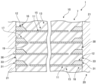
- FIG. 2 is a cross-sectional view schematically showing an active layer (laminate); The figure which shows the outline
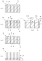
- FIG. 4 is a diagram showing an example of scanning traces of laser light; 4 is a flowchart showing an example of a method for manufacturing a capacitor;
- Fig. 1 shows an example of a capacitor according to the present invention.
- a capacitor (capacitor) 1 having a main body (main body portion, laminated body) 10 in which a plurality of dielectric layers and a plurality of electrode layers are alternately laminated and integrated, and an external electrode 20 connected to the main body 10 .
- a capacitor 1 whose appearance is shown in FIG. 1(a) is an example of a thin film polymer multilayer capacitor, and as shown in the cross-sectional view of FIG. , an active layer 7 that develops capacitance, a dummy layer 8 that does not develop capacitance disposed above and below it, and a protective layer 9 disposed above and below it.
- the active layer 7 and the dummy layer 8 are formed by alternately laminating a plurality of resin layers (dielectric layers) 13 and a plurality of electrode layers 11, and the protective layer 9 is made only of resin.
- the external electrodes 20 are formed by metal spraying (metallicon) so as to be bonded to the connection surfaces 30 where the ends of the multiple electrode layers 11 and the ends of the multiple resin layers 13 of the active layer 7 and the dummy layer 8 are exposed. It includes an inner metallikon layer (metal sprayed layer, eg, brass metallikon) 21, a copper plating layer 22 surrounding it, and a tin plating layer 23 covering the outside.
- FIG. 2 shows an enlarged cross section of a part of the active layer 7 of the main body 10 .
- the active layer 7 of the main body 10 is a portion in which a plurality of dielectric layers 13 and a plurality of electrode layers 11 are alternately laminated. (portions, edges, connection portions, connection regions, connection boundaries) 31 and ends 33 of the respective dielectric layers 13 are joined to the metallikon layers 21 of the external electrodes 20, and the respective electrode layers 11 are electrically metallikon layers. connected to layer 21;
- the electrode layer 11 is in wide contact with the dielectric layer 13 inside the active layer 7, and is an end where a thin-film internal electrode portion (internal electrode layer) 15 forming a capacitor and an external electrode 20 (metallikon layer 21) are connected.
- a portion 31 includes a heavy edge portion 16 thicker than the internal electrode portion 15 .
- the heavy edge portion 16 of the electrode layer 11 is composed of the electrode layer 11 and the layer 12 laminated on the electrode layer 11 . Therefore, the internal electrode layer 15 is composed of the electrode layer 11, the heavy edge portion 16 is composed of the electrode layer 11 and the laminated layer 12, the heavy edge portion 16 is connected to the internal electrode layer 15, and the heavy edge portion 16 is One end 31 is exposed to the connection surface 30 .
- the thickness of the internal electrode layer (internal electrode portion) 15 is preferably thin, for example, 0.01 ⁇ m, or even thinner, 0.005 ⁇ m (5 nm). may On the other hand, considering the connection with the external electrode 20, it is considered that a thickness of about 0.01 ⁇ m or more is necessary. may be provided. In addition, when the internal electrode portion 15 has a sufficient thickness, the heavy edge portion 16 may not be provided.
- An example of the resin forming the dielectric layer 13 is a thermosetting resin, including an acrylic polymer.
- An example of the resin that can be used for the thin-film polymer multilayer capacitor 1 is a polymer obtained by polymerizing one or more of tricyclodecanedimethanol dimethacrylate and tricyclodecanedimethanol diacrylate, which constitutes the dielectric layer 13. Resin is not limited to this.
- the dielectric layer 13 may be thin enough and the body portion 7 may have a sufficient number of laminations to provide a compact, thin, high-capacity capacitor.
- the thickness of the dielectric layer 13 may be 0.1 to 1.5 ⁇ m, or 0.2 to 1.2 ⁇ m, and the number of layers may be 1000 or more.
- the dielectric layer 13 having a predetermined thickness can be obtained by depositing a thermosetting resin as a monomer under a reduced pressure environment (in a vacuum) and curing it by irradiation with an electron beam or the like. can.
- a capacitor 1 having a dielectric layer 13 made of a thermosetting resin has a higher heat-resistant temperature than a capacitor made of a thermoplastic resin, and is compatible with reflow, so it can be provided as an element more suitable for surface mounting. .
- the electrode layer 11 may be made of at least one of conductive metals such as aluminum, zinc, copper, gold, silver, or alloys containing these.
- the withstand voltage can be improved by reducing the thickness of the electrodes functioning as a capacitor, that is, the internal electrode layers 15 .
- the withstand voltage may be 400 V or more, and the thickness of the internal electrode layer 15 may be about 3 to 50 nm, or about 5 to 30 nm.
- Surface resistivity may be used to control the thickness of the thin-film electrodes, and the surface resistivity of the internal electrode layer 15 may be 5 to 80 ⁇ /square ( ⁇ /sq.), preferably 15 to 60 ⁇ /square. It may be 20 to 50 ⁇ / ⁇ .
- the electrode layer 11 of the capacitor 1 may further include a dummy heavy edge portion 17 separated from the internal electrode layer 15 by a gap 19 and having one end exposed to the connection surface 30. good. Since the dummy heavy edge portion 17 is separated from the internal electrode layer 15 , it does not contribute to the capacitance of the capacitor 1 . However, it is useful for obtaining mechanical connection strength between the external electrode 20 and the metallikon (sprayed metal) 21, and maintains or maintains the connection with the metallikon 21 together with the heavy edge portion 16 integrated with the internal electrode layer 15. Strengthen. Therefore, in the following description, the end of the dummy heavy edge portion 17 is treated in common with the end 31 of the electrode layer 11 (dummy hedge portion 16).
- the layer 12 constituting the heavy edge portion 16 may be laminated on the upper side of the electrode layer 11, may be laminated on the lower side, or may be laminated on both upper and lower surfaces.
- the heavy edge portion 16 is not limited to a two-layer structure, and may have a one-layer structure or a structure of three or more layers.
- the withstand voltage can be increased, but the loss factor (tan ⁇ ) and the equivalent series resistance (ESR) increase, and the performance as a capacitor tends to deteriorate. Therefore, the configuration of the end (end portion) 31, which is the connecting portion between the electrode layer 11 and the external electrode 20, is important. Conventionally, even if the internal electrode portion 15 is thin, the tan ⁇ and ESR are lowered and the frequency characteristics are improved by securing a sufficient thickness of the end portion 31, which is the connection portion with the external electrode 20, metallikon 21 in this example. It was thought that it would improve and be able to handle high currents.
- the method of connecting the laminate (body) 10 and the external electrodes 20 is mostly the metallikon 21 as far as it is commercialized.
- metallikon 21 it is difficult to secure the mechanical strength necessary for a capacitor by means other than metal spraying, that is, metal spraying.
- the end (edge) 31 of the electrode is exposed, and at the same time, an anchoring effect is generated to obtain the bonding strength with the metallikon 21.
- the inventors of the present application believe that it is necessary to create the resulting uneven shape on the connecting surface 30 .
- the current standard for thin-film polymer multilayer capacitors is the ashing method that uses plasma, and the electrode lead-out shape is greatly affected by the state of the film formation and is affected by the uneven distribution of the plasma. It is considered difficult to obtain the shape. For this reason, the inventors of the present application assumed that it would be difficult to solve problems such as peeling of metallikon and poor electrical characteristics in the current mass production process that employs only the ashing method using plasma.
- Fig. 3 shows an overview of the assumed ashing mechanism. Ashing is originally a technique for uniformly etching organic matter. For this reason, a high ashing rate and a certain amount of ashing time are required to form unevenness. On the other hand, as the dielectric thickness increases, the ashing surface tends to become smoother, and no significant change is seen when the output or flow rate is changed. Therefore, it is considered that the reason why the unevenness is formed by ashing is that the energy of strong ashing is used to make the difference in the adhesion between layers visible. For example, even if the connection surface 30 in the initial state is flat as shown in FIG. 3A, the end portion 33 of the dielectric layer 13 is ashed as shown in FIG.
- the edges of the plurality of dielectric layers 13 to be metallikoned are coated. 33 and at least a portion of the connecting surface 30 where the ends 31 of the plurality of electrode layers 11 are exposed are scanned with laser light (laser, laser beam). As shown in FIG. 4A, the connection surface 30 of the main body 10 is scanned with a laser beam 51 emitted from a laser light source 50 .
- a strip-shaped (stick-shaped) cut surface from a laminate serving as the base of the main body 10 is scanned with a laser beam 51 as the connection surface 30 , and the laser beam 51 is scanned onto the connection surface 30 .
- the connection surface 30 is laser-processed by irradiation of . Spatial (two-dimensional or three-dimensional) periodic structure or shape change (difference) in the ends 31 of the plurality of electrode layers 11 and the ends 33 of the plurality of resin layers 13 exposed on the connecting surface 30 by laser processing is introduced, and is considered to contribute to strengthening of the adhesion to the external electrode 20 by the metallikon.
- Lasers for processing include YVO4 laser (wavelength 1064 nm), YAG laser (wavelength 1064 nm), fiber laser (wavelength 1090 nm), semiconductor laser (wavelength 650-905 nm), excimer laser (wavelength 193 nm) and CO2 laser (wavelength 10600 nm). Any of the following can be mentioned.
- semiconductor lasers include GaAs, GaAlAs, and GaInAs.
- the laser light 51 may be a pulse. Taking a YVO4 laser as an example, the output is 3 to 30 W, the scan speed is 100 to 10000 mm/s, the pulse frequency is 1 to 200 kHz, and the scan pitch is 0.01 to 0.01. It may be set to 2 mm.
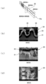
- FIG. 5 shows the results of electron microscope observation of the state of the connecting surface 30 scanned by the YVO4 laser 51 with an output of 10 W, a scan speed of 1000 mm, a pulse frequency of 40 kHz, and a scan pitch of 0.04 mm.
- S-3000H manufactured by Hitachi observed conditions: acceleration voltage 5 kV, working distance 15 mm
- FIG. 5(a) shows the position of the viewing surface.
- the laser processing is performed on the strip-shaped main body (stick-shaped main body) 10a before it is cut into chips, and the observation surface A in FIG. A cross section along the body portion 10a is shown, an observation surface B in FIG.
- FIG. 5C shows a cross section perpendicular to the stick-shaped main body portion 10a of the connection surface 30, and an observation surface C in FIG. It shows a plane along the stick-shaped body portion 10a of the face 30.
- the connecting surface 30 has continuous unevenness (macroscopic unevenness) 35 formed by scanning with the laser beam 51 , and furthermore, the electrode is formed from the edge 33 of the dielectric layer 13 . It can be seen that the edge 31 of the layer 11 is recessed to form microscopic unevenness 36 .
- FIG. 4(b) conceptually shows how the connection surface 30 scanned by the laser 51 also takes into account the observation results shown in FIG.
- a certain amount of the electrode layer 11 can be forcibly melted and evaporated, and the dielectric layer 13 can be melted and evaporated.
- macroscopic irregularities 35 can be formed (introduced) in the connecting surface 30 by this.
- the end 31 of the electrode layer 11 appearing on the connecting surface 30 can be selectively melted and transpired. It is considered possible. As a result, the edge 31 of the electrode layer 11 recedes with respect to the edge 33 of the dielectric layer 13, and it is possible to form the region 37 in which the interlayer of the dielectric layer 13 is open. For this reason, it is considered that a uniform uneven shape (microscopic uneven shape) 36 can be formed (introduced) at the edge 33 of the dielectric layer 13 and the edge 31 of the electrode layer 11 .
- the metallikon 21 evenly penetrates into the microscopic unevenness 36 in the region 37 formed between the layers and having the microscopic unevenness 36 having a layer thickness level, for example, a size of about 5 to 200 nm. It is considered that sufficient bonding strength and good electrical properties can be obtained even with a relatively shallow penetration depth.
- the edge 33 of the dielectric layer 13 and the edge 31 of the electrode layer 11 are both melted and transpired, resulting in a macroscopic size larger than the layer thickness level, for example, about 200 nm to 100 ⁇ m. unevenness 35 is formed. It is considered that the macroscopic unevenness 35 makes it possible to suppress peeling due to stress that may occur between the metallikon 21 and the connection surface 30 . Therefore, it is possible to manufacture the capacitor 1 having the metallikon 21 with sufficient bonding strength and good electrical characteristics to the main body 10 . For example, as shown in FIG.
- the macroscopic unevenness 35 is formed by narrowing the spot diameter of the laser beam 51 so that three-dimensional (three-dimensional) scanning traces 55 are formed on the connecting surface 30 at limited locations. It may be formed so as to be clearly visible as In addition, since it is possible to form the region 37 in which the microscopic unevenness 36 is formed in the concave portion of the macroscopic unevenness 35, the connection surface 30 can be formed by forming three-dimensional scanning traces 55 on the connecting surface 30 by laser processing. A region 37 having microscopic unevenness 36 can be formed on at least a portion of the surface 30 .
- FIG. 4 shows, as an example, the body portion 10 in which the thickness of the end 31 of the electrode layer 11 does not change, in order to schematically explain the outline of the laser processing.
- the laser treatment of the connection surface 30 even if the end 31 of the thick-film heavy edge portion 16 is exposed on the connection surface 30 with respect to the thin-film internal electrode layer 15, the same is considered to be the case.
- FIG. 6 A specific example of laser processing is shown in FIG.
- the spot diameter can be increased by defocusing (shifting the focus) as shown in FIGS. 6(a) and 6(c).
- FIG. 6B it is also possible to reduce the spot diameter by focusing the laser beam 51 on the connection surface 30.
- the connecting surface 30 may be scanned with the laser beam 51 in a state in which scanning traces do not clearly appear.
- a clear scanning trace of the laser beam 51 may be formed on the connection surface 30 .
- FIG. 7 shows some examples of scanning traces 55 of the laser beam 51 formed on the connection surface 30.
- FIG. FIGS. 7A to 7C show examples of scanning traces 55 consisting of a pattern of only oblique lines formed parallel or almost parallel.
- FIGS. 7(d) to (f) show examples of scanning traces 55 formed of patterns in which a plurality of lines intersect. The angle is shown with reference to the extending direction of the edge 33 of the dielectric layer 13 and the edge 31 of the electrode layer 11 appearing on the connection surface 30 .
- the scanning trace 55 shown in FIG. 7 is an example, and the scanning trace formed by the laser beam 51 is not limited to these examples.
- the conditions such as the spot diameter and pattern (scanning trace) of the laser beam 51 scanning the connection surface 30 can be selected according to the conditions such as the processing time required for processing the laser beam 51 and the adhesion to the metallikon 21 .
- the connection surface 30 may be scanned in parallel with a plurality of laser beams 51 .
- FIG. 8 shows a flow chart of the main part of a series of processes for manufacturing the capacitor 1 .
- a laminate that is the base of the main body 10 is manufactured.
- An example of a method of manufacturing a laminate is a method of forming each layer by a vapor deposition method. 11 are alternately formed to manufacture a laminate that is the base of the body portion 10 in which a plurality of dielectric layers 13 and a plurality of electrode layers 11 are alternately laminated.
- the laminate may be manufactured using other methods such as coating or printing.
- step 42 the laminate is cut into strips to form the main body portion 10a in a strip state (stick state).
- the strip-shaped body portion 10a may be formed directly from the laminate, or the strip-shaped body portion 10a may be manufactured through other processing such as a flattening press treatment or a card cutting treatment.
- step 43 the cut surface is scanned with the laser beam 51 as the connection surface 30 to be metallikoned.
- the spot of the laser beam 51 may be narrowed to form a scanning trace 55 by the laser beam 51 on the connecting surface 30 .
- step 43 by irradiating the connection surface 30 with the laser beam 51 , a plurality of dielectric layers 13 are formed on at least a part of the connection surface 30 with respect to the ends 33 of the plurality of dielectric layers 13 exposed on the connection surface 30 .
- the ends 31 of the electrode layer 11 each form recessed portions (microscopic unevenness) 36 .
- Each of the plurality of electrode layers 11 is connected to a thin film internal electrode layer 15 laminated inside the main body 10 , one of which is exposed to the connection surface 30 , and has a thick film heavy edge with respect to the internal electrode layer 15 .
- the portion 16 When the portion 16 is provided, the plurality of heavy edge portions 16 appearing on the connection surface 30 and the plurality of dielectric layers 13 may be scanned with the laser beam 51 .
- the edge 31 of the heavy edge portion 16 of the thickness of the internal electrode layer 15 can be melted and transpired by laser irradiation, and the comparison between the adjacent dielectric layer 13 corresponding to each heavy edge portion 16 can be performed.
- a large unevenness 36 can be formed.
- the metallikon 21 can enter evenly, and the metallikon 21 having sufficient bonding strength and good electrical properties can be manufactured.
- the dummy heavy edge portion 17 can also be subjected to the laser treatment in the same manner, and the adhesion between the contact surface 30 including the dummy heavy edge portion 17 and the external electrode 20 can be improved. can be improved.
- the contact surface 30 may be scanned with the laser beam 51 to form scanning traces 55 on the contact surface 30 with the laser beam 51 .
- the scan mark 55 may be a three-dimensional scan mark 55 , and macroscopic unevenness 35 can be introduced into the contact surface 30 .
- the microscopic unevenness is formed on at least a partial region 37 of the contact surface 30 . 36 can be formed.
- the external electrodes 20 are formed by metallikon (metal spraying) on the connection surface 30 scanned by the laser beam 51.
- suitable metallikon metals include zinc, tin, brass, and the like.
- the processing required for the external electrodes 20 such as heat treatment (step 45) and deburring (step 46) is performed.
- step 47 the strip-like body portion 10a with the external electrodes 20 formed thereon is cut into chips together with the external electrodes 20, thereby manufacturing the capacitor 1 in which the external electrodes 20 are connected to the body portion 10.
- FIG. 8 show typical treatments, and other treatments may be performed. good.
- the state of the connecting surface 30 may be controlled by performing plasma processing similar to the conventional one before and after the laser beam scanning processing (step 43).
- the external electrode 20 with sufficient bonding strength and good electrical characteristics can be manufactured by the laser beam scanning process (step 43) and the plasma treatment can be omitted, the processes from the cutting of the strip to the subsequent process can be performed in the air. can be done with Therefore, the manufacturing process of the capacitor can be further simplified. Therefore, the capacitor 1 having the body portion 10 in which the plurality of dielectric layers 13 and the plurality of electrode layers 11 are laminated, and the external electrode 20 connected to at least a part of the body portion 10 can be provided at a lower cost. can.
- the capacitor 1 manufactured by this manufacturing method may include traces 55 scanned by the laser beam 51 on at least a portion of the connection surface 30 of the main body 10 on which the external electrodes 20 are formed by the metallikon 21. .
- the connection surface 30 includes a plurality of heavy edge portions 16 appearing on the connection surface 30 and a plurality of dielectric layers. 13 and may include scan marks 55 .
- the plurality of electrode layers 11 or the ends 31 of the heavy edge portions 16 are formed on at least a part of the connection surface 30 of the body portion 10 on which the external electrodes 20 are formed by the metallikon 21 . At least a portion may include a region 37 formed with unevenness 36 recessed from at least a portion of the edges 33 of the plurality of dielectric layers 13 .
Landscapes
- Engineering & Computer Science (AREA)
- Power Engineering (AREA)
- Manufacturing & Machinery (AREA)
- Microelectronics & Electronic Packaging (AREA)
- Fixed Capacitors And Capacitor Manufacturing Machines (AREA)
- Physics & Mathematics (AREA)
- Optics & Photonics (AREA)
- Plasma & Fusion (AREA)
- Mechanical Engineering (AREA)
Priority Applications (4)
| Application Number | Priority Date | Filing Date | Title |
|---|---|---|---|
| JP2023561577A JP7708877B2 (ja) | 2021-11-16 | 2022-11-14 | コンデンサおよびその製造方法 |
| US18/710,546 US12597563B2 (en) | 2021-11-16 | 2022-11-14 | Capacitor and method for manufacturing the same |
| CN202280074872.5A CN118235220A (zh) | 2021-11-16 | 2022-11-14 | 电容器及其制造方法 |
| EP22895560.5A EP4435813A4 (en) | 2021-11-16 | 2022-11-14 | CAPACITOR AND ITS MANUFACTURING PROCESS |
Applications Claiming Priority (2)
| Application Number | Priority Date | Filing Date | Title |
|---|---|---|---|
| JP2021186331 | 2021-11-16 | ||
| JP2021-186331 | 2021-11-16 |
Publications (1)
| Publication Number | Publication Date |
|---|---|
| WO2023090278A1 true WO2023090278A1 (ja) | 2023-05-25 |
Family
ID=86396948
Family Applications (1)
| Application Number | Title | Priority Date | Filing Date |
|---|---|---|---|
| PCT/JP2022/042170 Ceased WO2023090278A1 (ja) | 2021-11-16 | 2022-11-14 | コンデンサおよびその製造方法 |
Country Status (5)
| Country | Link |
|---|---|
| US (1) | US12597563B2 (https=) |
| EP (1) | EP4435813A4 (https=) |
| JP (1) | JP7708877B2 (https=) |
| CN (1) | CN118235220A (https=) |
| WO (1) | WO2023090278A1 (https=) |
Citations (6)
| Publication number | Priority date | Publication date | Assignee | Title |
|---|---|---|---|---|
| JPH02129906A (ja) * | 1988-11-09 | 1990-05-18 | Matsushita Electric Ind Co Ltd | フィルムコンデンサの製造方法 |
| JPH04233217A (ja) * | 1990-12-28 | 1992-08-21 | Matsushita Electric Ind Co Ltd | 金属化フィルムコンデンサの製造方法および製造装置 |
| JP2003109837A (ja) * | 2001-09-28 | 2003-04-11 | Matsushita Electric Ind Co Ltd | 積層フィルムコンデンサと積層フィルムコンデンサの製造方法と積層フィルムコンデンサ製造装置 |
| JP2004006495A (ja) | 2002-05-31 | 2004-01-08 | Nichicon Corp | 積層フィルムコンデンサおよびその製造方法 |
| JP2013118356A (ja) * | 2011-10-31 | 2013-06-13 | Murata Mfg Co Ltd | セラミック電子部品及びその製造方法 |
| JP2015177172A (ja) * | 2014-03-18 | 2015-10-05 | 京セラ株式会社 | フィルムコンデンサ |
Family Cites Families (7)
| Publication number | Priority date | Publication date | Assignee | Title |
|---|---|---|---|---|
| DE19734477B4 (de) | 1996-08-09 | 2005-11-03 | Matsushita Electric Industrial Co., Ltd., Kadoma | Metallisierter Filmkondensator und Vorrichtung und Verfahren für die Herstellung eines metallisierten Films für den metallisierten Filmkondensator |
| US5912796A (en) * | 1996-11-15 | 1999-06-15 | Illinois Tool Works, Inc. | Metallized film capacitor and manufacturing process |
| JP2013004916A (ja) * | 2011-06-21 | 2013-01-07 | Daikin Ind Ltd | フィルムコンデンサ |
| FR2989007B1 (fr) * | 2012-04-04 | 2015-05-15 | M U L Micro Usinage Laser | Procede de metallisation d'une patte de connexion d'un composant electrique |
| DE102015117452B4 (de) | 2015-10-14 | 2024-10-02 | Semikron Elektronik Gmbh & Co. Kg | Folienkondensator und Verfahren zur Herstellung eines Folienkondensators |
| JP2018182039A (ja) * | 2017-04-12 | 2018-11-15 | 太陽誘電株式会社 | 積層セラミックコンデンサ及びその製造方法 |
| US11854748B2 (en) | 2021-11-26 | 2023-12-26 | Rubycon Corporation | Thin film high polymer laminated capacitor manufacturing method |
-
2022
- 2022-11-14 EP EP22895560.5A patent/EP4435813A4/en active Pending
- 2022-11-14 JP JP2023561577A patent/JP7708877B2/ja active Active
- 2022-11-14 WO PCT/JP2022/042170 patent/WO2023090278A1/ja not_active Ceased
- 2022-11-14 CN CN202280074872.5A patent/CN118235220A/zh active Pending
- 2022-11-14 US US18/710,546 patent/US12597563B2/en active Active
Patent Citations (6)
| Publication number | Priority date | Publication date | Assignee | Title |
|---|---|---|---|---|
| JPH02129906A (ja) * | 1988-11-09 | 1990-05-18 | Matsushita Electric Ind Co Ltd | フィルムコンデンサの製造方法 |
| JPH04233217A (ja) * | 1990-12-28 | 1992-08-21 | Matsushita Electric Ind Co Ltd | 金属化フィルムコンデンサの製造方法および製造装置 |
| JP2003109837A (ja) * | 2001-09-28 | 2003-04-11 | Matsushita Electric Ind Co Ltd | 積層フィルムコンデンサと積層フィルムコンデンサの製造方法と積層フィルムコンデンサ製造装置 |
| JP2004006495A (ja) | 2002-05-31 | 2004-01-08 | Nichicon Corp | 積層フィルムコンデンサおよびその製造方法 |
| JP2013118356A (ja) * | 2011-10-31 | 2013-06-13 | Murata Mfg Co Ltd | セラミック電子部品及びその製造方法 |
| JP2015177172A (ja) * | 2014-03-18 | 2015-10-05 | 京セラ株式会社 | フィルムコンデンサ |
Non-Patent Citations (1)
| Title |
|---|
| See also references of EP4435813A4 |
Also Published As
| Publication number | Publication date |
|---|---|
| US20250010400A1 (en) | 2025-01-09 |
| EP4435813A1 (en) | 2024-09-25 |
| US12597563B2 (en) | 2026-04-07 |
| JP7708877B2 (ja) | 2025-07-15 |
| CN118235220A (zh) | 2024-06-21 |
| EP4435813A4 (en) | 2025-11-05 |
| JPWO2023090278A1 (https=) | 2023-05-25 |
Similar Documents
| Publication | Publication Date | Title |
|---|---|---|
| EP2810539B1 (en) | Laser patterning of photovoltaic backsheet | |
| US20020158307A1 (en) | Laminated body, capacitor, electronic part, and method and device for manufacturing the laminated body, capacitor, and electronic part | |
| TWI544590B (zh) | 半導體裝置封裝體及其製造方法 | |
| US4898648A (en) | Method for providing a strengthened conductive circuit pattern | |
| US20240087815A1 (en) | Thin film high polymer laminated capacitor | |
| JP2000306771A (ja) | 電子部品及び電子部品の製造方法 | |
| KR100344482B1 (ko) | 프린트 기판 및 프린트 기판의 제조방법 | |
| WO2023090278A1 (ja) | コンデンサおよびその製造方法 | |
| TW586340B (en) | Laser processing method | |
| CN114425653A (zh) | 一种封装基板的激光加工方法及激光加工系统 | |
| JP4655574B2 (ja) | 電解コンデンサの製造方法 | |
| JP2006203077A5 (https=) | ||
| JP2010283062A (ja) | 固体電解コンデンサ及びその製造方法 | |
| JP2007522644A (ja) | レーザーを用いた受動電子部品の端子の形成方法 | |
| JP2004327830A (ja) | プリント基板の製造方法およびプリント基板 | |
| JP3979027B2 (ja) | セラミック電子部品の製造方法 | |
| JP2006041447A (ja) | 電解コンデンサの製造方法及び電解コンデンサ | |
| JP3869736B2 (ja) | レーザ加工方法及び多層配線基板 | |
| US12494324B2 (en) | Capacitor and method for manufacturing same | |
| TWI303148B (en) | Production method for electronic component and electronic component | |
| JPH04170016A (ja) | 積層セラミック電子部品の製造方法 | |
| JP2004063801A (ja) | 配線基板の製造方法および同製造方法に使用される基板 | |
| JPH03182078A (ja) | 電気的接続部材の製造方法 | |
| JP2004140403A (ja) | 電子部品の製造方法 | |
| JPH06246922A (ja) | インクジェット式記録ヘッドの製造方法 |
Legal Events
| Date | Code | Title | Description |
|---|---|---|---|
| 121 | Ep: the epo has been informed by wipo that ep was designated in this application |
Ref document number: 22895560 Country of ref document: EP Kind code of ref document: A1 |
|
| WWE | Wipo information: entry into national phase |
Ref document number: 2023561577 Country of ref document: JP |
|
| WWE | Wipo information: entry into national phase |
Ref document number: 202280074872.5 Country of ref document: CN |
|
| WWE | Wipo information: entry into national phase |
Ref document number: 18710546 Country of ref document: US |
|
| WWE | Wipo information: entry into national phase |
Ref document number: 2022895560 Country of ref document: EP |
|
| ENP | Entry into the national phase |
Ref document number: 2022895560 Country of ref document: EP Effective date: 20240617 |
|
| WWG | Wipo information: grant in national office |
Ref document number: 18710546 Country of ref document: US |