WO2023090278A1 - Capacitor and method for manufacturing same - Google Patents
Capacitor and method for manufacturing same Download PDFInfo
- Publication number
- WO2023090278A1 WO2023090278A1 PCT/JP2022/042170 JP2022042170W WO2023090278A1 WO 2023090278 A1 WO2023090278 A1 WO 2023090278A1 JP 2022042170 W JP2022042170 W JP 2022042170W WO 2023090278 A1 WO2023090278 A1 WO 2023090278A1
- Authority
- WO
- WIPO (PCT)
- Prior art keywords
- main body
- scanning
- connection surface
- capacitor
- layers
- Prior art date
Links
- 239000003990 capacitor Substances 0.000 title claims abstract description 57
- 238000004519 manufacturing process Methods 0.000 title claims description 29
- 238000000034 method Methods 0.000 title claims description 23
- 229910052751 metal Inorganic materials 0.000 claims abstract description 24
- 239000002184 metal Substances 0.000 claims abstract description 24
- 238000005507 spraying Methods 0.000 claims abstract description 18
- 229910009372 YVO4 Inorganic materials 0.000 claims description 5
- 238000005520 cutting process Methods 0.000 claims description 5
- 239000004065 semiconductor Substances 0.000 claims description 4
- 239000000835 fiber Substances 0.000 claims description 3
- 230000015572 biosynthetic process Effects 0.000 abstract description 5
- 239000010410 layer Substances 0.000 description 167
- 238000004380 ashing Methods 0.000 description 18
- 229920005989 resin Polymers 0.000 description 12
- 239000011347 resin Substances 0.000 description 12
- 239000010408 film Substances 0.000 description 10
- 239000010409 thin film Substances 0.000 description 10
- 229920000642 polymer Polymers 0.000 description 7
- 238000011282 treatment Methods 0.000 description 7
- 238000009832 plasma treatment Methods 0.000 description 6
- 230000001678 irradiating effect Effects 0.000 description 4
- 229910052782 aluminium Inorganic materials 0.000 description 3
- XAGFODPZIPBFFR-UHFFFAOYSA-N aluminium Chemical compound [Al] XAGFODPZIPBFFR-UHFFFAOYSA-N 0.000 description 3
- 238000013532 laser treatment Methods 0.000 description 3
- 239000001301 oxygen Substances 0.000 description 3
- 229910052760 oxygen Inorganic materials 0.000 description 3
- 229920001187 thermosetting polymer Polymers 0.000 description 3
- 229910001369 Brass Inorganic materials 0.000 description 2
- RYGMFSIKBFXOCR-UHFFFAOYSA-N Copper Chemical compound [Cu] RYGMFSIKBFXOCR-UHFFFAOYSA-N 0.000 description 2
- ATJFFYVFTNAWJD-UHFFFAOYSA-N Tin Chemical compound [Sn] ATJFFYVFTNAWJD-UHFFFAOYSA-N 0.000 description 2
- HCHKCACWOHOZIP-UHFFFAOYSA-N Zinc Chemical compound [Zn] HCHKCACWOHOZIP-UHFFFAOYSA-N 0.000 description 2
- 239000010951 brass Substances 0.000 description 2
- 229910052802 copper Inorganic materials 0.000 description 2
- 239000010949 copper Substances 0.000 description 2
- 230000032798 delamination Effects 0.000 description 2
- 230000000694 effects Effects 0.000 description 2
- 238000005530 etching Methods 0.000 description 2
- 238000003475 lamination Methods 0.000 description 2
- 150000002739 metals Chemical class 0.000 description 2
- 230000000737 periodic effect Effects 0.000 description 2
- 238000007747 plating Methods 0.000 description 2
- 239000011241 protective layer Substances 0.000 description 2
- 229910052718 tin Inorganic materials 0.000 description 2
- 239000011135 tin Substances 0.000 description 2
- 229910052725 zinc Inorganic materials 0.000 description 2
- 239000011701 zinc Substances 0.000 description 2
- -1 GaAlAs Inorganic materials 0.000 description 1
- 229910001218 Gallium arsenide Inorganic materials 0.000 description 1
- 229910000530 Gallium indium arsenide Inorganic materials 0.000 description 1
- BQCADISMDOOEFD-UHFFFAOYSA-N Silver Chemical compound [Ag] BQCADISMDOOEFD-UHFFFAOYSA-N 0.000 description 1
- VEBCLRKUSAGCDF-UHFFFAOYSA-N ac1mi23b Chemical compound C1C2C3C(COC(=O)C=C)CCC3C1C(COC(=O)C=C)C2 VEBCLRKUSAGCDF-UHFFFAOYSA-N 0.000 description 1
- 230000001133 acceleration Effects 0.000 description 1
- 230000003213 activating effect Effects 0.000 description 1
- 229910045601 alloy Inorganic materials 0.000 description 1
- 239000000956 alloy Substances 0.000 description 1
- 238000004458 analytical method Methods 0.000 description 1
- 238000004873 anchoring Methods 0.000 description 1
- QVGXLLKOCUKJST-UHFFFAOYSA-N atomic oxygen Chemical compound [O] QVGXLLKOCUKJST-UHFFFAOYSA-N 0.000 description 1
- 239000011248 coating agent Substances 0.000 description 1
- 238000000576 coating method Methods 0.000 description 1
- 238000000151 deposition Methods 0.000 description 1
- 238000010586 diagram Methods 0.000 description 1
- 238000009826 distribution Methods 0.000 description 1
- 238000001312 dry etching Methods 0.000 description 1
- 238000010894 electron beam technology Methods 0.000 description 1
- 239000007789 gas Substances 0.000 description 1
- PCHJSUWPFVWCPO-UHFFFAOYSA-N gold Chemical compound [Au] PCHJSUWPFVWCPO-UHFFFAOYSA-N 0.000 description 1
- 229910052737 gold Inorganic materials 0.000 description 1
- 239000010931 gold Substances 0.000 description 1
- 238000010438 heat treatment Methods 0.000 description 1
- 239000011229 interlayer Substances 0.000 description 1
- 238000005304 joining Methods 0.000 description 1
- 238000010030 laminating Methods 0.000 description 1
- 239000011104 metalized film Substances 0.000 description 1
- 238000012986 modification Methods 0.000 description 1
- 230000004048 modification Effects 0.000 description 1
- 239000000178 monomer Substances 0.000 description 1
- OTLDLKLSNZMTTA-UHFFFAOYSA-N octahydro-1h-4,7-methanoindene-1,5-diyldimethanol Chemical compound C1C2C3C(CO)CCC3C1C(CO)C2 OTLDLKLSNZMTTA-UHFFFAOYSA-N 0.000 description 1
- 239000005416 organic matter Substances 0.000 description 1
- 230000035515 penetration Effects 0.000 description 1
- 229920000058 polyacrylate Polymers 0.000 description 1
- 230000000379 polymerizing effect Effects 0.000 description 1
- 229910052709 silver Inorganic materials 0.000 description 1
- 239000004332 silver Substances 0.000 description 1
- 238000005728 strengthening Methods 0.000 description 1
- 238000004381 surface treatment Methods 0.000 description 1
- 229920005992 thermoplastic resin Polymers 0.000 description 1
- 238000007740 vapor deposition Methods 0.000 description 1
Images


Classifications
-
- H—ELECTRICITY
- H01—ELECTRIC ELEMENTS
- H01G—CAPACITORS; CAPACITORS, RECTIFIERS, DETECTORS, SWITCHING DEVICES OR LIGHT-SENSITIVE DEVICES, OF THE ELECTROLYTIC TYPE
- H01G4/00—Fixed capacitors; Processes of their manufacture
- H01G4/002—Details
- H01G4/228—Terminals
-
- H—ELECTRICITY
- H01—ELECTRIC ELEMENTS
- H01G—CAPACITORS; CAPACITORS, RECTIFIERS, DETECTORS, SWITCHING DEVICES OR LIGHT-SENSITIVE DEVICES, OF THE ELECTROLYTIC TYPE
- H01G4/00—Fixed capacitors; Processes of their manufacture
- H01G4/002—Details
- H01G4/228—Terminals
- H01G4/232—Terminals electrically connecting two or more layers of a stacked or rolled capacitor
-
- H—ELECTRICITY
- H01—ELECTRIC ELEMENTS
- H01G—CAPACITORS; CAPACITORS, RECTIFIERS, DETECTORS, SWITCHING DEVICES OR LIGHT-SENSITIVE DEVICES, OF THE ELECTROLYTIC TYPE
- H01G4/00—Fixed capacitors; Processes of their manufacture
- H01G4/002—Details
- H01G4/228—Terminals
- H01G4/252—Terminals the terminals being coated on the capacitive element
-
- H—ELECTRICITY
- H01—ELECTRIC ELEMENTS
- H01G—CAPACITORS; CAPACITORS, RECTIFIERS, DETECTORS, SWITCHING DEVICES OR LIGHT-SENSITIVE DEVICES, OF THE ELECTROLYTIC TYPE
- H01G4/00—Fixed capacitors; Processes of their manufacture
- H01G4/30—Stacked capacitors
-
- H—ELECTRICITY
- H01—ELECTRIC ELEMENTS
- H01G—CAPACITORS; CAPACITORS, RECTIFIERS, DETECTORS, SWITCHING DEVICES OR LIGHT-SENSITIVE DEVICES, OF THE ELECTROLYTIC TYPE
- H01G4/00—Fixed capacitors; Processes of their manufacture
- H01G4/32—Wound capacitors
Definitions
- the present invention relates to a capacitor and its manufacturing method.
- Japanese Patent Laid-Open No. 2004-6495 discloses that after a laminate base body in which aluminum is deposited on a dielectric resin layer and alternately laminated is cut into sticks, two or more of CF 3 , CF 4 and O 2 are added.
- a lamination characterized by activating the contained mixed gas to a plasma state, chemically dry-etching the cut surface to an etching depth of 10 to 100 ⁇ m, and forming an electrode lead-out portion by metal spraying on the etched surface.
- a metallized film capacitor and method of making the same are disclosed.
- Multilayer capacitors are small, have high withstand voltage, and low ESR. Furthermore, it is important that the connection with the external electrode is good and stable, and that good withstand voltage characteristics are obtained.
- thin film polymer multilayer capacitors can have dielectric layers as thin as 1.5 ⁇ m or less, and can provide compact capacitors with high withstand voltage and low ESR.
- the connection portion with the external electrode will also be thin. For this reason, the connection resistance of the connection portion becomes high, making it difficult to sufficiently reduce the ESR. Adopting a heavy edge structure in which only the edge portion is made thicker is also under consideration. In order to provide a compact capacitor with a high withstand voltage and a lower connection resistance, it is important to further stabilize the connection with the external electrodes.
- One aspect of the present invention is a method of manufacturing a capacitor having a main body in which a plurality of dielectric layers and a plurality of electrode layers are alternately laminated, and an external electrode connected to at least part of the main body.
- the connecting surfaces of the main body to be metal sprayed are connected so that the ends of the plurality of dielectric layers and the plurality of electrode layers are exposed. At least part of the surface is scanned with a laser beam. Scanning the connecting surface with a laser beam (scanning step, scanning treatment) may be used instead of or together with a surface treatment with plasma.
- connection surface By irradiating the connection surface with a laser beam, the connection surface can be processed such that the structure and/or shape of at least a part of the connection surface are repeatedly changed at appropriate intervals (pitch). For example, in order to obtain a stable connection with an external electrode formed by metal spraying, the connection surface may be stably formed with an uneven shape.
- plasma processing is basically ashing of the dielectric layer, and the amount of ashing depends on the film formation state of the dielectric layer. Variation in quantity is likely to occur. Therefore, it is difficult to control the state of the electrode layer on the connection surface by plasma treatment or only by plasma treatment.
- the connection surface is scanned with a laser beam. In this method, not only the edge of the dielectric layer but also the edge of the electrode layer can be forcibly melted and transpired. Configurations or shapes can be introduced periodically in two or three dimensions.
- the processing (process, step) of scanning with a laser beam may include forming a scanning mark with a laser beam on the connecting surface.
- the scanning mark may be a three-dimensional scanning mark.
- the processing of scanning with a laser beam may include forming unevenness on at least part of the connecting surface. For example, by scanning the connection surface with a laser beam having a relatively large spot diameter, irregularities may be formed depending on the film formation state of the dielectric layer and/or the electrode layer. As another example, by scanning with a laser beam having a relatively small spot diameter, it is possible to form a scanning trace with unevenness in a predetermined direction or shape, and forcibly form unevenness in a predetermined shape on the connection surface. good too.
- the scanning process forms, on at least a portion of the connection surface, a region in which at least a portion of the edges of the plurality of electrode layers are recessed relative to at least a portion of the edges of the plurality of dielectric layers exposed on the connection surface.
- the electrode layer made of a metal such as aluminum may evaporate more easily than the dielectric layer by laser irradiation.
- a concavo-convex structure having high connectivity with may be formed.
- Each of the plurality of electrode layers may be connected to the internal electrode layer laminated inside the main body, and may have a thick heavy edge portion with respect to the internal electrode layer, one end of which is exposed to the connection surface.
- the scanning process may include scanning the ends of the plurality of heavy edge portions and the ends of the plurality of dielectric layers appearing on the connecting surface with a laser beam. If the electrode layer appearing on the connection surface becomes too thick, the connectivity with the external electrode tends to deteriorate. In addition, since the thicker heavy edge portion recedes due to the laser irradiation, the unevenness between the dielectric layer and the electrode layer is likely to increase, and the connectivity with the external electrode can be improved.
- At least one of a YVO4 laser, a YAG laser, a fiber laser, a semiconductor laser, an excimer laser, and a CO2 laser can be used as the laser light used for the scanning process.
- this manufacturing method may further include the following steps. - Producing a laminate by alternately forming a plurality of dielectric layers and a plurality of electrode layers. - To form a main body portion in a strip state (stick state) cut from a laminate. ⁇ Scan the cut surface with a laser beam as a connecting surface. • Forming external electrodes by metal spraying on the connection surface scanned by the laser beam. - Cutting the strip-like main body on which the external electrodes are formed into chips together with the external electrodes. If the plasma treatment can be omitted by using the laser beam scanning treatment, it becomes possible to carry out the treatments after the strip cutting in the atmosphere, which further simplifies the manufacturing process of the capacitor. Therefore, the capacitor can be provided at a lower cost.
- Another aspect of the present invention is a capacitor having a main body in which a plurality of dielectric layers and a plurality of electrode layers are laminated, and an external electrode connected to at least a part of the main body.
- At least a portion of the connection surface of the main body of the capacitor, on which the external electrodes are formed by metal spraying, includes traces of laser light scanning.
- the plurality of electrode layers may be connected to the internal electrode layers laminated inside the main body, one end of which may be exposed to the connection surface, and a thick heavy edge portion with respect to the internal electrode layers.
- the connecting surface may include scanning traces across the ends of the plurality of heavy edge portions appearing on the connecting surface and the ends of the plurality of dielectric layers.
- Another aspect of the present invention is a capacitor having a main body in which a plurality of dielectric layers and a plurality of electrode layers are laminated, and an external electrode connected to at least a part of the main body, At least a portion of the connection surface of the main body on which the external electrodes are formed by metal spraying includes unevenness in which at least a portion of the ends of the plurality of electrode layers recedes with respect to a portion of the ends of the plurality of dielectric layers.
- a capacitor Each of the plurality of electrode layers of this capacitor is connected to the internal electrode layer laminated inside the main body, one end is exposed to the connection surface, and the internal electrode layer is provided with a thick-film heavy edge portion. and at least some of the ends of the plurality of heavy edge portions appearing on the connecting surface may recede with respect to some of the ends of the plurality of dielectric layers.
- FIG. 2 is a cross-sectional view schematically showing an active layer (laminate); The figure which shows the outline
- FIG. 4 is a diagram showing an example of scanning traces of laser light; 4 is a flowchart showing an example of a method for manufacturing a capacitor;
- Fig. 1 shows an example of a capacitor according to the present invention.
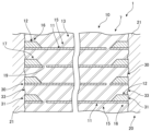
- a capacitor (capacitor) 1 having a main body (main body portion, laminated body) 10 in which a plurality of dielectric layers and a plurality of electrode layers are alternately laminated and integrated, and an external electrode 20 connected to the main body 10 .
- a capacitor 1 whose appearance is shown in FIG. 1(a) is an example of a thin film polymer multilayer capacitor, and as shown in the cross-sectional view of FIG. , an active layer 7 that develops capacitance, a dummy layer 8 that does not develop capacitance disposed above and below it, and a protective layer 9 disposed above and below it.
- the active layer 7 and the dummy layer 8 are formed by alternately laminating a plurality of resin layers (dielectric layers) 13 and a plurality of electrode layers 11, and the protective layer 9 is made only of resin.
- the external electrodes 20 are formed by metal spraying (metallicon) so as to be bonded to the connection surfaces 30 where the ends of the multiple electrode layers 11 and the ends of the multiple resin layers 13 of the active layer 7 and the dummy layer 8 are exposed. It includes an inner metallikon layer (metal sprayed layer, eg, brass metallikon) 21, a copper plating layer 22 surrounding it, and a tin plating layer 23 covering the outside.
- FIG. 2 shows an enlarged cross section of a part of the active layer 7 of the main body 10 .
- the active layer 7 of the main body 10 is a portion in which a plurality of dielectric layers 13 and a plurality of electrode layers 11 are alternately laminated. (portions, edges, connection portions, connection regions, connection boundaries) 31 and ends 33 of the respective dielectric layers 13 are joined to the metallikon layers 21 of the external electrodes 20, and the respective electrode layers 11 are electrically metallikon layers. connected to layer 21;
- the electrode layer 11 is in wide contact with the dielectric layer 13 inside the active layer 7, and is an end where a thin-film internal electrode portion (internal electrode layer) 15 forming a capacitor and an external electrode 20 (metallikon layer 21) are connected.
- a portion 31 includes a heavy edge portion 16 thicker than the internal electrode portion 15 .
- the heavy edge portion 16 of the electrode layer 11 is composed of the electrode layer 11 and the layer 12 laminated on the electrode layer 11 . Therefore, the internal electrode layer 15 is composed of the electrode layer 11, the heavy edge portion 16 is composed of the electrode layer 11 and the laminated layer 12, the heavy edge portion 16 is connected to the internal electrode layer 15, and the heavy edge portion 16 is One end 31 is exposed to the connection surface 30 .
- the thickness of the internal electrode layer (internal electrode portion) 15 is preferably thin, for example, 0.01 ⁇ m, or even thinner, 0.005 ⁇ m (5 nm). may On the other hand, considering the connection with the external electrode 20, it is considered that a thickness of about 0.01 ⁇ m or more is necessary. may be provided. In addition, when the internal electrode portion 15 has a sufficient thickness, the heavy edge portion 16 may not be provided.
- An example of the resin forming the dielectric layer 13 is a thermosetting resin, including an acrylic polymer.
- An example of the resin that can be used for the thin-film polymer multilayer capacitor 1 is a polymer obtained by polymerizing one or more of tricyclodecanedimethanol dimethacrylate and tricyclodecanedimethanol diacrylate, which constitutes the dielectric layer 13. Resin is not limited to this.
- the dielectric layer 13 may be thin enough and the body portion 7 may have a sufficient number of laminations to provide a compact, thin, high-capacity capacitor.
- the thickness of the dielectric layer 13 may be 0.1 to 1.5 ⁇ m, or 0.2 to 1.2 ⁇ m, and the number of layers may be 1000 or more.
- the dielectric layer 13 having a predetermined thickness can be obtained by depositing a thermosetting resin as a monomer under a reduced pressure environment (in a vacuum) and curing it by irradiation with an electron beam or the like. can.
- a capacitor 1 having a dielectric layer 13 made of a thermosetting resin has a higher heat-resistant temperature than a capacitor made of a thermoplastic resin, and is compatible with reflow, so it can be provided as an element more suitable for surface mounting. .
- the electrode layer 11 may be made of at least one of conductive metals such as aluminum, zinc, copper, gold, silver, or alloys containing these.
- the withstand voltage can be improved by reducing the thickness of the electrodes functioning as a capacitor, that is, the internal electrode layers 15 .
- the withstand voltage may be 400 V or more, and the thickness of the internal electrode layer 15 may be about 3 to 50 nm, or about 5 to 30 nm.
- Surface resistivity may be used to control the thickness of the thin-film electrodes, and the surface resistivity of the internal electrode layer 15 may be 5 to 80 ⁇ /square ( ⁇ /sq.), preferably 15 to 60 ⁇ /square. It may be 20 to 50 ⁇ / ⁇ .
- the electrode layer 11 of the capacitor 1 may further include a dummy heavy edge portion 17 separated from the internal electrode layer 15 by a gap 19 and having one end exposed to the connection surface 30. good. Since the dummy heavy edge portion 17 is separated from the internal electrode layer 15 , it does not contribute to the capacitance of the capacitor 1 . However, it is useful for obtaining mechanical connection strength between the external electrode 20 and the metallikon (sprayed metal) 21, and maintains or maintains the connection with the metallikon 21 together with the heavy edge portion 16 integrated with the internal electrode layer 15. Strengthen. Therefore, in the following description, the end of the dummy heavy edge portion 17 is treated in common with the end 31 of the electrode layer 11 (dummy hedge portion 16).
- the layer 12 constituting the heavy edge portion 16 may be laminated on the upper side of the electrode layer 11, may be laminated on the lower side, or may be laminated on both upper and lower surfaces.
- the heavy edge portion 16 is not limited to a two-layer structure, and may have a one-layer structure or a structure of three or more layers.
- the withstand voltage can be increased, but the loss factor (tan ⁇ ) and the equivalent series resistance (ESR) increase, and the performance as a capacitor tends to deteriorate. Therefore, the configuration of the end (end portion) 31, which is the connecting portion between the electrode layer 11 and the external electrode 20, is important. Conventionally, even if the internal electrode portion 15 is thin, the tan ⁇ and ESR are lowered and the frequency characteristics are improved by securing a sufficient thickness of the end portion 31, which is the connection portion with the external electrode 20, metallikon 21 in this example. It was thought that it would improve and be able to handle high currents.
- the method of connecting the laminate (body) 10 and the external electrodes 20 is mostly the metallikon 21 as far as it is commercialized.
- metallikon 21 it is difficult to secure the mechanical strength necessary for a capacitor by means other than metal spraying, that is, metal spraying.
- the end (edge) 31 of the electrode is exposed, and at the same time, an anchoring effect is generated to obtain the bonding strength with the metallikon 21.
- the inventors of the present application believe that it is necessary to create the resulting uneven shape on the connecting surface 30 .
- the current standard for thin-film polymer multilayer capacitors is the ashing method that uses plasma, and the electrode lead-out shape is greatly affected by the state of the film formation and is affected by the uneven distribution of the plasma. It is considered difficult to obtain the shape. For this reason, the inventors of the present application assumed that it would be difficult to solve problems such as peeling of metallikon and poor electrical characteristics in the current mass production process that employs only the ashing method using plasma.
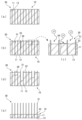
- Fig. 3 shows an overview of the assumed ashing mechanism. Ashing is originally a technique for uniformly etching organic matter. For this reason, a high ashing rate and a certain amount of ashing time are required to form unevenness. On the other hand, as the dielectric thickness increases, the ashing surface tends to become smoother, and no significant change is seen when the output or flow rate is changed. Therefore, it is considered that the reason why the unevenness is formed by ashing is that the energy of strong ashing is used to make the difference in the adhesion between layers visible. For example, even if the connection surface 30 in the initial state is flat as shown in FIG. 3A, the end portion 33 of the dielectric layer 13 is ashed as shown in FIG.
- the edges of the plurality of dielectric layers 13 to be metallikoned are coated. 33 and at least a portion of the connecting surface 30 where the ends 31 of the plurality of electrode layers 11 are exposed are scanned with laser light (laser, laser beam). As shown in FIG. 4A, the connection surface 30 of the main body 10 is scanned with a laser beam 51 emitted from a laser light source 50 .
- a strip-shaped (stick-shaped) cut surface from a laminate serving as the base of the main body 10 is scanned with a laser beam 51 as the connection surface 30 , and the laser beam 51 is scanned onto the connection surface 30 .
- the connection surface 30 is laser-processed by irradiation of . Spatial (two-dimensional or three-dimensional) periodic structure or shape change (difference) in the ends 31 of the plurality of electrode layers 11 and the ends 33 of the plurality of resin layers 13 exposed on the connecting surface 30 by laser processing is introduced, and is considered to contribute to strengthening of the adhesion to the external electrode 20 by the metallikon.
- Lasers for processing include YVO4 laser (wavelength 1064 nm), YAG laser (wavelength 1064 nm), fiber laser (wavelength 1090 nm), semiconductor laser (wavelength 650-905 nm), excimer laser (wavelength 193 nm) and CO2 laser (wavelength 10600 nm). Any of the following can be mentioned.
- semiconductor lasers include GaAs, GaAlAs, and GaInAs.
- the laser light 51 may be a pulse. Taking a YVO4 laser as an example, the output is 3 to 30 W, the scan speed is 100 to 10000 mm/s, the pulse frequency is 1 to 200 kHz, and the scan pitch is 0.01 to 0.01. It may be set to 2 mm.
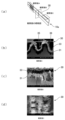
- FIG. 5 shows the results of electron microscope observation of the state of the connecting surface 30 scanned by the YVO4 laser 51 with an output of 10 W, a scan speed of 1000 mm, a pulse frequency of 40 kHz, and a scan pitch of 0.04 mm.
- S-3000H manufactured by Hitachi observed conditions: acceleration voltage 5 kV, working distance 15 mm
- FIG. 5(a) shows the position of the viewing surface.
- the laser processing is performed on the strip-shaped main body (stick-shaped main body) 10a before it is cut into chips, and the observation surface A in FIG. A cross section along the body portion 10a is shown, an observation surface B in FIG.
- FIG. 5C shows a cross section perpendicular to the stick-shaped main body portion 10a of the connection surface 30, and an observation surface C in FIG. It shows a plane along the stick-shaped body portion 10a of the face 30.
- the connecting surface 30 has continuous unevenness (macroscopic unevenness) 35 formed by scanning with the laser beam 51 , and furthermore, the electrode is formed from the edge 33 of the dielectric layer 13 . It can be seen that the edge 31 of the layer 11 is recessed to form microscopic unevenness 36 .
- FIG. 4(b) conceptually shows how the connection surface 30 scanned by the laser 51 also takes into account the observation results shown in FIG.
- a certain amount of the electrode layer 11 can be forcibly melted and evaporated, and the dielectric layer 13 can be melted and evaporated.
- macroscopic irregularities 35 can be formed (introduced) in the connecting surface 30 by this.
- the end 31 of the electrode layer 11 appearing on the connecting surface 30 can be selectively melted and transpired. It is considered possible. As a result, the edge 31 of the electrode layer 11 recedes with respect to the edge 33 of the dielectric layer 13, and it is possible to form the region 37 in which the interlayer of the dielectric layer 13 is open. For this reason, it is considered that a uniform uneven shape (microscopic uneven shape) 36 can be formed (introduced) at the edge 33 of the dielectric layer 13 and the edge 31 of the electrode layer 11 .
- the metallikon 21 evenly penetrates into the microscopic unevenness 36 in the region 37 formed between the layers and having the microscopic unevenness 36 having a layer thickness level, for example, a size of about 5 to 200 nm. It is considered that sufficient bonding strength and good electrical properties can be obtained even with a relatively shallow penetration depth.
- the edge 33 of the dielectric layer 13 and the edge 31 of the electrode layer 11 are both melted and transpired, resulting in a macroscopic size larger than the layer thickness level, for example, about 200 nm to 100 ⁇ m. unevenness 35 is formed. It is considered that the macroscopic unevenness 35 makes it possible to suppress peeling due to stress that may occur between the metallikon 21 and the connection surface 30 . Therefore, it is possible to manufacture the capacitor 1 having the metallikon 21 with sufficient bonding strength and good electrical characteristics to the main body 10 . For example, as shown in FIG.
- the macroscopic unevenness 35 is formed by narrowing the spot diameter of the laser beam 51 so that three-dimensional (three-dimensional) scanning traces 55 are formed on the connecting surface 30 at limited locations. It may be formed so as to be clearly visible as In addition, since it is possible to form the region 37 in which the microscopic unevenness 36 is formed in the concave portion of the macroscopic unevenness 35, the connection surface 30 can be formed by forming three-dimensional scanning traces 55 on the connecting surface 30 by laser processing. A region 37 having microscopic unevenness 36 can be formed on at least a portion of the surface 30 .
- FIG. 4 shows, as an example, the body portion 10 in which the thickness of the end 31 of the electrode layer 11 does not change, in order to schematically explain the outline of the laser processing.
- the laser treatment of the connection surface 30 even if the end 31 of the thick-film heavy edge portion 16 is exposed on the connection surface 30 with respect to the thin-film internal electrode layer 15, the same is considered to be the case.
- FIG. 6 A specific example of laser processing is shown in FIG.
- the spot diameter can be increased by defocusing (shifting the focus) as shown in FIGS. 6(a) and 6(c).
- FIG. 6B it is also possible to reduce the spot diameter by focusing the laser beam 51 on the connection surface 30.
- the connecting surface 30 may be scanned with the laser beam 51 in a state in which scanning traces do not clearly appear.
- a clear scanning trace of the laser beam 51 may be formed on the connection surface 30 .
- FIG. 7 shows some examples of scanning traces 55 of the laser beam 51 formed on the connection surface 30.
- FIG. FIGS. 7A to 7C show examples of scanning traces 55 consisting of a pattern of only oblique lines formed parallel or almost parallel.
- FIGS. 7(d) to (f) show examples of scanning traces 55 formed of patterns in which a plurality of lines intersect. The angle is shown with reference to the extending direction of the edge 33 of the dielectric layer 13 and the edge 31 of the electrode layer 11 appearing on the connection surface 30 .
- the scanning trace 55 shown in FIG. 7 is an example, and the scanning trace formed by the laser beam 51 is not limited to these examples.
- the conditions such as the spot diameter and pattern (scanning trace) of the laser beam 51 scanning the connection surface 30 can be selected according to the conditions such as the processing time required for processing the laser beam 51 and the adhesion to the metallikon 21 .
- the connection surface 30 may be scanned in parallel with a plurality of laser beams 51 .
- FIG. 8 shows a flow chart of the main part of a series of processes for manufacturing the capacitor 1 .
- a laminate that is the base of the main body 10 is manufactured.
- An example of a method of manufacturing a laminate is a method of forming each layer by a vapor deposition method. 11 are alternately formed to manufacture a laminate that is the base of the body portion 10 in which a plurality of dielectric layers 13 and a plurality of electrode layers 11 are alternately laminated.
- the laminate may be manufactured using other methods such as coating or printing.
- step 42 the laminate is cut into strips to form the main body portion 10a in a strip state (stick state).
- the strip-shaped body portion 10a may be formed directly from the laminate, or the strip-shaped body portion 10a may be manufactured through other processing such as a flattening press treatment or a card cutting treatment.
- step 43 the cut surface is scanned with the laser beam 51 as the connection surface 30 to be metallikoned.
- the spot of the laser beam 51 may be narrowed to form a scanning trace 55 by the laser beam 51 on the connecting surface 30 .
- step 43 by irradiating the connection surface 30 with the laser beam 51 , a plurality of dielectric layers 13 are formed on at least a part of the connection surface 30 with respect to the ends 33 of the plurality of dielectric layers 13 exposed on the connection surface 30 .
- the ends 31 of the electrode layer 11 each form recessed portions (microscopic unevenness) 36 .
- Each of the plurality of electrode layers 11 is connected to a thin film internal electrode layer 15 laminated inside the main body 10 , one of which is exposed to the connection surface 30 , and has a thick film heavy edge with respect to the internal electrode layer 15 .
- the portion 16 When the portion 16 is provided, the plurality of heavy edge portions 16 appearing on the connection surface 30 and the plurality of dielectric layers 13 may be scanned with the laser beam 51 .
- the edge 31 of the heavy edge portion 16 of the thickness of the internal electrode layer 15 can be melted and transpired by laser irradiation, and the comparison between the adjacent dielectric layer 13 corresponding to each heavy edge portion 16 can be performed.
- a large unevenness 36 can be formed.
- the metallikon 21 can enter evenly, and the metallikon 21 having sufficient bonding strength and good electrical properties can be manufactured.
- the dummy heavy edge portion 17 can also be subjected to the laser treatment in the same manner, and the adhesion between the contact surface 30 including the dummy heavy edge portion 17 and the external electrode 20 can be improved. can be improved.
- the contact surface 30 may be scanned with the laser beam 51 to form scanning traces 55 on the contact surface 30 with the laser beam 51 .
- the scan mark 55 may be a three-dimensional scan mark 55 , and macroscopic unevenness 35 can be introduced into the contact surface 30 .
- the microscopic unevenness is formed on at least a partial region 37 of the contact surface 30 . 36 can be formed.
- the external electrodes 20 are formed by metallikon (metal spraying) on the connection surface 30 scanned by the laser beam 51.
- suitable metallikon metals include zinc, tin, brass, and the like.
- the processing required for the external electrodes 20 such as heat treatment (step 45) and deburring (step 46) is performed.
- step 47 the strip-like body portion 10a with the external electrodes 20 formed thereon is cut into chips together with the external electrodes 20, thereby manufacturing the capacitor 1 in which the external electrodes 20 are connected to the body portion 10.
- FIG. 8 show typical treatments, and other treatments may be performed. good.
- the state of the connecting surface 30 may be controlled by performing plasma processing similar to the conventional one before and after the laser beam scanning processing (step 43).
- the external electrode 20 with sufficient bonding strength and good electrical characteristics can be manufactured by the laser beam scanning process (step 43) and the plasma treatment can be omitted, the processes from the cutting of the strip to the subsequent process can be performed in the air. can be done with Therefore, the manufacturing process of the capacitor can be further simplified. Therefore, the capacitor 1 having the body portion 10 in which the plurality of dielectric layers 13 and the plurality of electrode layers 11 are laminated, and the external electrode 20 connected to at least a part of the body portion 10 can be provided at a lower cost. can.
- the capacitor 1 manufactured by this manufacturing method may include traces 55 scanned by the laser beam 51 on at least a portion of the connection surface 30 of the main body 10 on which the external electrodes 20 are formed by the metallikon 21. .
- the connection surface 30 includes a plurality of heavy edge portions 16 appearing on the connection surface 30 and a plurality of dielectric layers. 13 and may include scan marks 55 .
- the plurality of electrode layers 11 or the ends 31 of the heavy edge portions 16 are formed on at least a part of the connection surface 30 of the body portion 10 on which the external electrodes 20 are formed by the metallikon 21 . At least a portion may include a region 37 formed with unevenness 36 recessed from at least a portion of the edges 33 of the plurality of dielectric layers 13 .
Abstract
Provided is a capacitor (1) having a main body (10) in which a plurality of dielectric layers (13) and a plurality of electrode layers (11) are laminated, and an external electrode (20) connected to at least part of the main body, wherein, prior to formation of the external electrode by metal spraying (metallikon) on the main body, at least part of a connection surface (30) to be subjected to metal spraying is scanned by a laser beam (51), and a scanning mark (55) composed of a relief (35) produced by the laser beam is formed in at least part of the connection surface.
Description
本発明は、コンデンサおよびその製造方法に関するものである。
The present invention relates to a capacitor and its manufacturing method.
日本国特開2004-6495号公報には、誘電体樹脂層にアルミニウムを蒸着し交互に重ね合わせた積層母体を、スティック状に切断した後、CF3、CF4、O2の2種以上を含有する混合ガスを活性化してプラズマ状態とし、該切断面にエッチング深さ10~100μmにケミカルドライエッチング処理を行い、該エッチング面に金属溶射して電極引出し部を形成したことを特徴とする積層金属化フィルムコンデンサおよびその製造方法が開示されている。
Japanese Patent Laid-Open No. 2004-6495 discloses that after a laminate base body in which aluminum is deposited on a dielectric resin layer and alternately laminated is cut into sticks, two or more of CF 3 , CF 4 and O 2 are added. A lamination characterized by activating the contained mixed gas to a plasma state, chemically dry-etching the cut surface to an etching depth of 10 to 100 μm, and forming an electrode lead-out portion by metal spraying on the etched surface. A metallized film capacitor and method of making the same are disclosed.
積層型のコンデンサは、小型で、高耐電圧、低ESRのものが提供されている。さらに、外部電極との接続性が良好で安定し、良好な耐電圧特性が得られることが重要となっている。例えば、フィルムコンデンサに対し、薄膜高分子積層コンデンサは誘電体層の厚みを1.5μm、あるいはそれ以下に薄くすることが可能であり、小型で、高耐電圧、低ESRのコンデンサを提供できる。一方、耐電圧を高めるためにコンデンサ部分の電極部分(内部電極部分)の表面抵抗率(シート抵抗率)を十分に高くなるように薄膜化すると外部電極との接続部分も薄くなる。このため、接続部分の接続抵抗は高くなり、ESRを十分に小さくすることが難しくなる。エッジ部分だけをさらに厚膜にしたヘビーエッジ構造を採用することも検討されている。小型、高耐電圧で、接続抵抗がさらに低いコンデンサを提供するためには、外部電極との接続をさらに安定させることが重要となっている。
Multilayer capacitors are small, have high withstand voltage, and low ESR. Furthermore, it is important that the connection with the external electrode is good and stable, and that good withstand voltage characteristics are obtained. For example, in contrast to film capacitors, thin film polymer multilayer capacitors can have dielectric layers as thin as 1.5 μm or less, and can provide compact capacitors with high withstand voltage and low ESR. On the other hand, if the surface resistivity (sheet resistivity) of the electrode portion (internal electrode portion) of the capacitor portion is made sufficiently high in order to increase the withstand voltage, the connection portion with the external electrode will also be thin. For this reason, the connection resistance of the connection portion becomes high, making it difficult to sufficiently reduce the ESR. Adopting a heavy edge structure in which only the edge portion is made thicker is also under consideration. In order to provide a compact capacitor with a high withstand voltage and a lower connection resistance, it is important to further stabilize the connection with the external electrodes.
本発明の一態様は、複数の誘電体層と複数の電極層とが交互に積層された本体部と、本体部の少なくとも一部に接続された外部電極とを有するコンデンサの製造方法である。この製造方法は、本体部に金属溶射により外部電極を形成する前に、金属溶射の対象とする本体部の接続面であって、複数の誘電体層および複数の電極層の端が露出した接続面の少なくとも一部をレーザー光により走査することを有する。レーザー光により接続面を走査すること(走査する工程、走査する処理)は、プラズマによる表面処理の代わりに、またはプラズマによる処理と共に用いられてもよい。接続面にレーザー光を照射することにより、接続面の少なくとも一部の構造および/または形状の変化が適当な間隔(ピッチ)で繰り返されるように接続面を加工できる。例えば、金属溶射により形成される外部電極との安定した接続を得るためには接続面に凹凸形状が安定して形成されてもよい。レーザー光による処理に対し、プラズマによる処理は、基本的には誘電体層のアッシングであり、アッシングの量は誘電体層の成膜状態に依存し、さらに、プラズマの分布に偏りが生ずるため処理量にばらつきが生じやすい。そのため、プラズマ処理により、あるいはプラズマ処理のみにより、接続面における電極層の状態を制御することが難しい。本発明においては、レーザー光により接続面を走査する。この方法では、強制的に、誘電体層の端だけではなく、電極層の端を含めて溶融蒸散させることが可能であり、接続面に、より安定して、金属溶射との接続性の高い構成または形状を2次元または3次元で周期的に導入できる。
One aspect of the present invention is a method of manufacturing a capacitor having a main body in which a plurality of dielectric layers and a plurality of electrode layers are alternately laminated, and an external electrode connected to at least part of the main body. In this manufacturing method, prior to forming the external electrodes on the main body by metal spraying, the connecting surfaces of the main body to be metal sprayed are connected so that the ends of the plurality of dielectric layers and the plurality of electrode layers are exposed. At least part of the surface is scanned with a laser beam. Scanning the connecting surface with a laser beam (scanning step, scanning treatment) may be used instead of or together with a surface treatment with plasma. By irradiating the connection surface with a laser beam, the connection surface can be processed such that the structure and/or shape of at least a part of the connection surface are repeatedly changed at appropriate intervals (pitch). For example, in order to obtain a stable connection with an external electrode formed by metal spraying, the connection surface may be stably formed with an uneven shape. In contrast to laser light processing, plasma processing is basically ashing of the dielectric layer, and the amount of ashing depends on the film formation state of the dielectric layer. Variation in quantity is likely to occur. Therefore, it is difficult to control the state of the electrode layer on the connection surface by plasma treatment or only by plasma treatment. In the present invention, the connection surface is scanned with a laser beam. In this method, not only the edge of the dielectric layer but also the edge of the electrode layer can be forcibly melted and transpired. Configurations or shapes can be introduced periodically in two or three dimensions.
レーザー光により走査する処理(工程、ステップ)は、接続面にレーザー光による走査痕を形成することを含んでいてもよい。走査痕は立体的な走査痕であってもよい。レーザー光により走査する処理は、接続面の少なくとも一部に凹凸を形成することを含んでいてもよい。一例としては、接続面を比較的スポット径の大きなレーザー光により走査することにより、誘電体層および/または電極層の成膜状態による凹凸が形成されることがある。他の例としては、比較的スポット径の小さなレーザー光により走査することにより、所定の方向あるいは形状の凹凸のある走査痕を形成でき、接続面に強制的に所定の形状の凹凸を形成してもよい。
The processing (process, step) of scanning with a laser beam may include forming a scanning mark with a laser beam on the connecting surface. The scanning mark may be a three-dimensional scanning mark. The processing of scanning with a laser beam may include forming unevenness on at least part of the connecting surface. For example, by scanning the connection surface with a laser beam having a relatively large spot diameter, irregularities may be formed depending on the film formation state of the dielectric layer and/or the electrode layer. As another example, by scanning with a laser beam having a relatively small spot diameter, it is possible to form a scanning trace with unevenness in a predetermined direction or shape, and forcibly form unevenness in a predetermined shape on the connection surface. good too.
走査する処理は、接続面の少なくとも一部に、接続面に露出した複数の誘電体層の端の少なくとも一部に対して、複数の電極層の端の少なくとも一部が後退した領域を形成することを含んでもよい。アルミニウムなどの金属で形成される電極層は、レーザー照射により、誘電体層よりも蒸散しやすくてもよく、レーザー照射により電極層の端が誘電体層の端よりも後退することで、金属溶射との接続性の高い凹凸構造が形成されてもよい。
The scanning process forms, on at least a portion of the connection surface, a region in which at least a portion of the edges of the plurality of electrode layers are recessed relative to at least a portion of the edges of the plurality of dielectric layers exposed on the connection surface. may include The electrode layer made of a metal such as aluminum may evaporate more easily than the dielectric layer by laser irradiation. A concavo-convex structure having high connectivity with may be formed.
複数の電極層のそれぞれは、本体部の内部に積層された内部電極層に繋がり、一方の端が接続面に露出した、内部電極層に対して厚膜のヘビーエッジ部を備えていてもよく、走査する処理は、接続面に現れた複数のヘビーエッジ部の端と複数の誘電体層の端とをレーザー光により走査することを含んでもよい。接続面に現れる電極層が厚くなりすぎると、外部電極との接続性が低下しやすいが、レーザー光を照射して安定した凹凸を作ることで接続性の低下を抑制できる。また、より膜厚のヘビーエッジ部がレーザー照射により後退することで、誘電体層と電極層との凹凸がより大きくなりやすく、外部電極との接続性を向上できる。
Each of the plurality of electrode layers may be connected to the internal electrode layer laminated inside the main body, and may have a thick heavy edge portion with respect to the internal electrode layer, one end of which is exposed to the connection surface. , the scanning process may include scanning the ends of the plurality of heavy edge portions and the ends of the plurality of dielectric layers appearing on the connecting surface with a laser beam. If the electrode layer appearing on the connection surface becomes too thick, the connectivity with the external electrode tends to deteriorate. In addition, since the thicker heavy edge portion recedes due to the laser irradiation, the unevenness between the dielectric layer and the electrode layer is likely to increase, and the connectivity with the external electrode can be improved.
走査する処理に用いられるレーザー光としては、YVO4レーザー、YAGレーザー、ファイバーレーザー、半導体レーザー、エキシマレーザーおよびCO2レーザーの少なくともいずれかを挙げることができる。
At least one of a YVO4 laser, a YAG laser, a fiber laser, a semiconductor laser, an excimer laser, and a CO2 laser can be used as the laser light used for the scanning process.
また、この製造方法は、以下のステップをさらに含んでいてもよい。
・複数の誘電体層と複数の電極層とを交互に成膜して積層体を製造すること。
・積層体から条切断された条状態(スティック状態)の本体部を形成すること。
・条切断された面を接続面としてレーザー光により走査すること。
・レーザー光により走査された接続面に金属溶射により外部電極を形成すること。
・外部電極が形成された条状態の本体部を外部電極とともにチップ状にカットすること。レーザー光により走査する処理を用いることによりプラズマ処理が省略できる場合は、条切断から以降の処理を大気中で行うことが可能となり、コンデンサの製造工程をより簡略化できる。このため、さらに低コストでコンデンサを提供できる。 Moreover, this manufacturing method may further include the following steps.
- Producing a laminate by alternately forming a plurality of dielectric layers and a plurality of electrode layers.
- To form a main body portion in a strip state (stick state) cut from a laminate.
・Scan the cut surface with a laser beam as a connecting surface.
• Forming external electrodes by metal spraying on the connection surface scanned by the laser beam.
- Cutting the strip-like main body on which the external electrodes are formed into chips together with the external electrodes. If the plasma treatment can be omitted by using the laser beam scanning treatment, it becomes possible to carry out the treatments after the strip cutting in the atmosphere, which further simplifies the manufacturing process of the capacitor. Therefore, the capacitor can be provided at a lower cost.
本発明の他の態様の1つは、複数の誘電体層と複数の電極層とが積層された本体部と、本体部の少なくとも一部に接続された外部電極とを有するコンデンサである。このコンデンサの本体部の、金属溶射により外部電極が形成された接続面の少なくとも一部に、レーザー光による走査痕を含む。複数の電極層は、本体部の内部に積層された内部電極層に繋がり、一方の端が接続面に露出し、内部電極層に対して厚膜のヘビーエッジ部を備えていてもよい。接続面には、接続面に現れた複数のヘビーエッジ部の端と、複数の誘電体層の端とにわたる走査痕を含んでもよい。
Another aspect of the present invention is a capacitor having a main body in which a plurality of dielectric layers and a plurality of electrode layers are laminated, and an external electrode connected to at least a part of the main body. At least a portion of the connection surface of the main body of the capacitor, on which the external electrodes are formed by metal spraying, includes traces of laser light scanning. The plurality of electrode layers may be connected to the internal electrode layers laminated inside the main body, one end of which may be exposed to the connection surface, and a thick heavy edge portion with respect to the internal electrode layers. The connecting surface may include scanning traces across the ends of the plurality of heavy edge portions appearing on the connecting surface and the ends of the plurality of dielectric layers.
本発明の他の態様の1つは、複数の誘電体層と複数の電極層とが積層された本体部と、本体部の少なくとも一部に接続された外部電極とを有するコンデンサであって、本体部の、金属溶射により外部電極が形成された接続面の少なくとも一部に、複数の電極層の端の少なくとも一部が複数の誘電体層の端の一部に対して後退した凹凸を含むコンデンサである。このコンデンサの複数の電極層のそれぞれは、本体部の内部に積層された内部電極層に繋がり、一方の端が接続面に露出し、内部電極層に対して厚膜のヘビーエッジ部を備えており、接続面に現れた複数のヘビーエッジ部の端の少なくとも一部が複数の誘電体層の端の一部に対して後退していてもよい。
Another aspect of the present invention is a capacitor having a main body in which a plurality of dielectric layers and a plurality of electrode layers are laminated, and an external electrode connected to at least a part of the main body, At least a portion of the connection surface of the main body on which the external electrodes are formed by metal spraying includes unevenness in which at least a portion of the ends of the plurality of electrode layers recedes with respect to a portion of the ends of the plurality of dielectric layers. is a capacitor. Each of the plurality of electrode layers of this capacitor is connected to the internal electrode layer laminated inside the main body, one end is exposed to the connection surface, and the internal electrode layer is provided with a thick-film heavy edge portion. and at least some of the ends of the plurality of heavy edge portions appearing on the connecting surface may recede with respect to some of the ends of the plurality of dielectric layers.
図1に、本発明に係るコンデンサの一例を示している。複数の誘電体層と複数の電極層とが交互に積層されて一体となった本体(本体部、積層体)10と、本体10に接続された外部電極20とを有するコンデンサ(キャパシタ)1として、薄膜高分子積層コンデンサが知られている。図1(a)に外観を示したコンデンサ1は、薄膜高分子積層コンデンサの一例であり、図1(b)に断面図で示すように、本体部10は、厚み方向の中央に設けられた、容量を発現するアクティブ層7と、その上下に配置された容量を発現しないダミー層8と、その上下に配置された保護層9とを含む。アクティブ層7およびダミー層8は、複数の樹脂層(誘電体層)13と複数の電極層11とが交互に積層された構成であり、保護層9は樹脂のみにより構成されている。外部電極20は、アクティブ層7およびダミー層8の複数の電極層11の端および複数の樹脂層13の端が現れた接続面30に接合するように金属溶射(メタリコン)で形成されており、内部のメタリコン層(金属溶射層、例えば、真鍮メタリコン)21と、その周囲を覆う銅メッキ層22と、さらに外側を覆う錫メッキ層23とを含む。
Fig. 1 shows an example of a capacitor according to the present invention. As a capacitor (capacitor) 1 having a main body (main body portion, laminated body) 10 in which a plurality of dielectric layers and a plurality of electrode layers are alternately laminated and integrated, and an external electrode 20 connected to the main body 10 , thin film polymer multilayer capacitors are known. A capacitor 1 whose appearance is shown in FIG. 1(a) is an example of a thin film polymer multilayer capacitor, and as shown in the cross-sectional view of FIG. , an active layer 7 that develops capacitance, a dummy layer 8 that does not develop capacitance disposed above and below it, and a protective layer 9 disposed above and below it. The active layer 7 and the dummy layer 8 are formed by alternately laminating a plurality of resin layers (dielectric layers) 13 and a plurality of electrode layers 11, and the protective layer 9 is made only of resin. The external electrodes 20 are formed by metal spraying (metallicon) so as to be bonded to the connection surfaces 30 where the ends of the multiple electrode layers 11 and the ends of the multiple resin layers 13 of the active layer 7 and the dummy layer 8 are exposed. It includes an inner metallikon layer (metal sprayed layer, eg, brass metallikon) 21, a copper plating layer 22 surrounding it, and a tin plating layer 23 covering the outside.
図2に、本体部10のアクティブ層7の一部の断面を拡大して示している。本体10のアクティブ層7は、複数の誘電体層13と複数の電極層11とが交互に積層された部分であり、理想的には、接続面30において、それぞれの電極層11の端(端部、エッジ部、接続部分、接続領域、接続境界)31と、それぞれの誘電体層13の端33とが外部電極20のメタリコン層21と接合し、それぞれの電極層11は電気的にもメタリコン層21と接続される。電極層11は、アクティブ層7の内部で誘電体層13と広く接し、容量を形成する薄膜状の内部電極部分(内部電極層)15と、外部電極20(メタリコン層21)とが接続する端31の部分が内部電極部分15よりも厚くなったヘビーエッジ部16とを含む。本例において電極層11のヘビーエッジ部16は電極層11と、電極層11に積層された層12とにより構成されている。したがって、内部電極層15は電極層11により構成され、ヘビーエッジ部16は電極層11と積層された層12とにより構成され、ヘビーエッジ部16は内部電極層15に繋がり、ヘビーエッジ部16の一方の端31が接続面30に露出した構成となっている。高耐電圧のコンデンサ1を提供する場合、内部電極層(内部電極部分)15の厚みは薄いことが望ましく、例えば、0.01μmであってもよく、さらに薄く、0.005μm(5nm)であってもよい。一方、外部電極20との接続を考慮すると、0.01μm程度あるいはそれ以上の厚みが必要であると考えられており、薄膜タイプの内部電極部分15を備えたコンデンサ1においては、ヘビーエッジ部16が設けられていてもよい。なお、内部電極部分15が十分な厚みを備えている場合は、ヘビーエッジ部16が設けられていなくてもよい。
FIG. 2 shows an enlarged cross section of a part of the active layer 7 of the main body 10 . The active layer 7 of the main body 10 is a portion in which a plurality of dielectric layers 13 and a plurality of electrode layers 11 are alternately laminated. (portions, edges, connection portions, connection regions, connection boundaries) 31 and ends 33 of the respective dielectric layers 13 are joined to the metallikon layers 21 of the external electrodes 20, and the respective electrode layers 11 are electrically metallikon layers. connected to layer 21; The electrode layer 11 is in wide contact with the dielectric layer 13 inside the active layer 7, and is an end where a thin-film internal electrode portion (internal electrode layer) 15 forming a capacitor and an external electrode 20 (metallikon layer 21) are connected. A portion 31 includes a heavy edge portion 16 thicker than the internal electrode portion 15 . In this example, the heavy edge portion 16 of the electrode layer 11 is composed of the electrode layer 11 and the layer 12 laminated on the electrode layer 11 . Therefore, the internal electrode layer 15 is composed of the electrode layer 11, the heavy edge portion 16 is composed of the electrode layer 11 and the laminated layer 12, the heavy edge portion 16 is connected to the internal electrode layer 15, and the heavy edge portion 16 is One end 31 is exposed to the connection surface 30 . When providing a capacitor 1 with a high withstand voltage, the thickness of the internal electrode layer (internal electrode portion) 15 is preferably thin, for example, 0.01 μm, or even thinner, 0.005 μm (5 nm). may On the other hand, considering the connection with the external electrode 20, it is considered that a thickness of about 0.01 μm or more is necessary. may be provided. In addition, when the internal electrode portion 15 has a sufficient thickness, the heavy edge portion 16 may not be provided.
誘電体層13を構成する樹脂の一例は熱硬化性樹脂であり、アクリル系ポリマーを含む。薄膜高分子積層コンデンサ1に採用可能な樹脂の一例は、トリシクロデカンジメタノールジメタクリレートまたはトリシクロデカンジメタノールジアクリレートのいずれか一種以上が重合したものであるが、誘電体層13を構成する樹脂はこれに限定されない。小型で薄く、大容量のコンデンサを提供するために、誘電体層13が十分に薄く、本体部7が十分な積層数を備えていてもよい。例えば、誘電体層13の厚みは0.1~1.5μmであってもよく、0.2~1.2μmであってもよく、積層数は1000あるいはそれ以上であってもよい。薄膜の誘電体層13は、熱硬化性樹脂を減圧環境下(真空中)でモノマとして蒸着し、電子線等を照射して硬化させることにより、所定の厚みの誘電体層13を得ることができる。熱硬化型の樹脂による誘電体層13を備えたコンデンサ1は、熱可塑性樹脂を備えたものと比較して耐熱温度が高く、リフローにも対応できるので、より表面実装に適した素子として提供できる。
An example of the resin forming the dielectric layer 13 is a thermosetting resin, including an acrylic polymer. An example of the resin that can be used for the thin-film polymer multilayer capacitor 1 is a polymer obtained by polymerizing one or more of tricyclodecanedimethanol dimethacrylate and tricyclodecanedimethanol diacrylate, which constitutes the dielectric layer 13. Resin is not limited to this. The dielectric layer 13 may be thin enough and the body portion 7 may have a sufficient number of laminations to provide a compact, thin, high-capacity capacitor. For example, the thickness of the dielectric layer 13 may be 0.1 to 1.5 μm, or 0.2 to 1.2 μm, and the number of layers may be 1000 or more. The dielectric layer 13 having a predetermined thickness can be obtained by depositing a thermosetting resin as a monomer under a reduced pressure environment (in a vacuum) and curing it by irradiation with an electron beam or the like. can. A capacitor 1 having a dielectric layer 13 made of a thermosetting resin has a higher heat-resistant temperature than a capacitor made of a thermoplastic resin, and is compatible with reflow, so it can be provided as an element more suitable for surface mounting. .
電極層11は、導電性の金属、例えば、アルミニウム、亜鉛、銅、金、銀、またはこれらを含む合金の少なくともいずれかにより形成してもよい。高圧用のコンデンサ1としては、コンデンサとして機能する電極、すなわち内部電極層15の厚みを薄くすることで耐電圧を向上できる。例えば、耐電圧は400V以上であってもよく、内部電極層15の厚みは3~50nm程度であってもよく、5~30nm程度であってもよい。薄膜状の電極の厚みの管理として表面抵抗率を用いてもよく、内部電極層15の表面抵抗率は5~80Ω/□(Ω/sq.)であってもよく、15~60Ω/□であってもよく、20~50Ω/□であってもよい。
The electrode layer 11 may be made of at least one of conductive metals such as aluminum, zinc, copper, gold, silver, or alloys containing these. As for the capacitor 1 for high voltage, the withstand voltage can be improved by reducing the thickness of the electrodes functioning as a capacitor, that is, the internal electrode layers 15 . For example, the withstand voltage may be 400 V or more, and the thickness of the internal electrode layer 15 may be about 3 to 50 nm, or about 5 to 30 nm. Surface resistivity may be used to control the thickness of the thin-film electrodes, and the surface resistivity of the internal electrode layer 15 may be 5 to 80 Ω/square (Ω/sq.), preferably 15 to 60 Ω/square. It may be 20 to 50 Ω/□.
コンデンサ1の電極層11は、さらに、内部電極層15から間隙19により分離されたダミーのヘビーエッジ部17であって、一方の端が接続面30に露出したダミーのヘビーエッジ部17を含んでもよい。ダミーのヘビーエッジ部17は、内部電極層15から分離されているのでコンデンサ1の容量としては寄与しない。しかしながら、外部電極20のメタリコン(金属溶射)21との機械的な接続強度を得るためには有用であり、内部電極層15と一体となったヘビーエッジ部16とともにメタリコン21との接続を維持あるいは強化する。したがって、以降においては、ダミーのヘビーエッジ部17の端も、電極層11(ダミーヘッジ部16)の端31と共通に扱って説明する。なお、本例では、ヘビーエッジ部16を構成する層12は、電極層11の上側に積層されていてもよく、下側に積層されていてもよく、上下両面に積層されていてもよい。ヘビーエッジ部16は2層構造に限らず、1層構造であってもよく、3層以上の構造であってもよい。
The electrode layer 11 of the capacitor 1 may further include a dummy heavy edge portion 17 separated from the internal electrode layer 15 by a gap 19 and having one end exposed to the connection surface 30. good. Since the dummy heavy edge portion 17 is separated from the internal electrode layer 15 , it does not contribute to the capacitance of the capacitor 1 . However, it is useful for obtaining mechanical connection strength between the external electrode 20 and the metallikon (sprayed metal) 21, and maintains or maintains the connection with the metallikon 21 together with the heavy edge portion 16 integrated with the internal electrode layer 15. Strengthen. Therefore, in the following description, the end of the dummy heavy edge portion 17 is treated in common with the end 31 of the electrode layer 11 (dummy hedge portion 16). In this example, the layer 12 constituting the heavy edge portion 16 may be laminated on the upper side of the electrode layer 11, may be laminated on the lower side, or may be laminated on both upper and lower surfaces. The heavy edge portion 16 is not limited to a two-layer structure, and may have a one-layer structure or a structure of three or more layers.
電極層11を薄膜にすると耐電圧は高くできるが、損失係数(tanδ)および等価直列抵抗分(ESR)が高くなり、コンデンサとしての性能が低下しやすい。このため、電極層11と外部電極20との接続部分である端(端部)31の構成は重要である。従来、内部電極部分15が薄くても、外部電極20、本例においてはメタリコン21との接続部分である端部31の厚みを十分に確保することにより、tanδおよびESRが低下し、周波数特性が向上し、高電流に対応可能となると考えられていた。
When the electrode layer 11 is thin, the withstand voltage can be increased, but the loss factor (tan δ) and the equivalent series resistance (ESR) increase, and the performance as a capacitor tends to deteriorate. Therefore, the configuration of the end (end portion) 31, which is the connecting portion between the electrode layer 11 and the external electrode 20, is important. Conventionally, even if the internal electrode portion 15 is thin, the tan δ and ESR are lowered and the frequency characteristics are improved by securing a sufficient thickness of the end portion 31, which is the connection portion with the external electrode 20, metallikon 21 in this example. It was thought that it would improve and be able to handle high currents.
フィルムコンデンサや薄膜高分子積層コンデンサなどの積層タイプのコンデンサにおいて、積層体(本体)10と外部電極20とを接続する手法は、商品化されている範囲ではメタリコン21がほとんどである。メタリコン、すなわち金属溶射以外の手法では、コンデンサとして必要な機械的強度を確保することが難しいのが現状である。メタリコンによる電極引出では、電極層11と外部電極20とを電気的に接合するために、電極の端(端部)31を露出させると同時に、メタリコン21との接合強度を得るためにアンカー効果が得られる凹凸形状を接続面30に作り出す必要があると本願の発明者らは考えている。薄膜高分子積層コンデンサにおいて現在標準となっているプラズマを使ったアッシング方法による電極引出形状では、製膜の状態に大きく左右されたり、プラズマの分布の偏りの影響を受けたりするため、安定した凹凸形状を得ることが難しいと考えられる。このため、プラズマを使ったアッシング方法のみを採用している現在の量産工程では、メタリコン剥離や電気特性不良などの問題を解決することが難しいと、本願の発明者らは想定した。
In laminated type capacitors such as film capacitors and thin film polymer multilayer capacitors, the method of connecting the laminate (body) 10 and the external electrodes 20 is mostly the metallikon 21 as far as it is commercialized. At present, it is difficult to secure the mechanical strength necessary for a capacitor by means other than metal spraying, that is, metal spraying. In order to electrically connect the electrode layer 11 and the external electrode 20, the end (edge) 31 of the electrode is exposed, and at the same time, an anchoring effect is generated to obtain the bonding strength with the metallikon 21. The inventors of the present application believe that it is necessary to create the resulting uneven shape on the connecting surface 30 . The current standard for thin-film polymer multilayer capacitors is the ashing method that uses plasma, and the electrode lead-out shape is greatly affected by the state of the film formation and is affected by the uneven distribution of the plasma. It is considered difficult to obtain the shape. For this reason, the inventors of the present application assumed that it would be difficult to solve problems such as peeling of metallikon and poor electrical characteristics in the current mass production process that employs only the ashing method using plasma.
酸素プラズマを用いたプラズマ処理(アッシング方式)では、各層のプラズマのエネルギーに対する密着力のバラツキを利用することにより凹凸形状を実現していると考えられる。すなわち、密着力の弱い層は容易に剥離するため、アッシングが深くまで進み、強い層はアッシングがあまり進行しないことで凹凸形状が形成されると考えられる。このため、アッシングにより形成される凹凸形状は、各層の製膜状態に強く依存され、各層の密着力が均一であればあるほど、凹凸形状を得ることが困難となってしまう。
In the plasma treatment (ashing method) using oxygen plasma, it is believed that unevenness is achieved by utilizing the variation in the adhesiveness of each layer to the energy of the plasma. In other words, since the layer with weak adhesion is easily peeled off, the ashing progresses deeply, and the layer with strong adhesion does not progress so much, so that the uneven shape is formed. Therefore, the uneven shape formed by ashing strongly depends on the film formation state of each layer, and the more uniform the adhesion of each layer, the more difficult it becomes to obtain the uneven shape.
図3に、想定されるアッシングのメカニズムの概要を示している。アッシングは元々均一に有機物をエッチングするための技術である。このため、凹凸を形成するためには高いアッシングレートと、ある程度のアッシング時間とが必要である。一方、誘電体厚が厚くなる程、平滑なアッシング面になる傾向があり、出力、流量変更ではあまり大きな変化は見られない。したがって、アッシングにより凹凸が形成される要因は、強いアッシングによるエネルギーを利用して、層間密着力の差を顕在化させることであると考えられる。例えば、図3(a)のように、初期状態の接続面30が平坦であっても、図3(b)に示すようにアッシングにより、誘電体層13の端部33がアッシングされるとともに、電極層11の端部31との間に層間剥離が発生することが、本願の発明者らによるメタリコンとの結合部分の解析で明らかになっている。この現象は、図3(c)に示すように、酸素ラジカルによる灰化反応やプラズマの熱などにより誘電体層13の端部33が収縮するためと想定される。図3(d)に示すように、剥離層39は酸素ラジカルの触れる面が増大することにより、アッシングが進み、接続面30に凹凸が形成されると考えられる。
Fig. 3 shows an overview of the assumed ashing mechanism. Ashing is originally a technique for uniformly etching organic matter. For this reason, a high ashing rate and a certain amount of ashing time are required to form unevenness. On the other hand, as the dielectric thickness increases, the ashing surface tends to become smoother, and no significant change is seen when the output or flow rate is changed. Therefore, it is considered that the reason why the unevenness is formed by ashing is that the energy of strong ashing is used to make the difference in the adhesion between layers visible. For example, even if the connection surface 30 in the initial state is flat as shown in FIG. 3A, the end portion 33 of the dielectric layer 13 is ashed as shown in FIG. It has been clarified by the analysis of the joint portion with the metallikon by the inventors of the present application that delamination occurs between the end portion 31 of the electrode layer 11 and the electrode layer 11 . As shown in FIG. 3C, this phenomenon is assumed to be caused by shrinkage of the end portion 33 of the dielectric layer 13 due to an ashing reaction due to oxygen radicals, plasma heat, or the like. As shown in FIG. 3(d), it is considered that the contact surface of the peeling layer 39 with oxygen radicals increases, so ashing progresses and the connecting surface 30 becomes uneven.
一方、図3(e)に示すように、プラズマのエネルギーが層間剥離の差を発生させるためには不足または過剰な状態であると、均一にアッシングが進み、接続面30に凹凸が形成されず、電極層11のみが露出した状態となる。このため、誘電体層13と外部電極20との接合力が得られず、外部電極20を安定して維持するための密着力が得られない可能性がある。
On the other hand, as shown in FIG. 3(e), if the plasma energy is insufficient or excessive to cause a difference in delamination, the ashing progresses uniformly, and unevenness is not formed on the connecting surface 30. , only the electrode layer 11 is exposed. For this reason, the bonding strength between the dielectric layer 13 and the external electrodes 20 cannot be obtained, and there is a possibility that the adhesion strength for stably maintaining the external electrodes 20 cannot be obtained.
図4に示すように、本発明においては、プラズマによる処理の代わりに、あるいはプラズマによる処理に加えて、メタリコン(金属溶射)に先立って、メタリコンの対象となる、複数の誘電体層13の端33および複数の電極層11の端31が露出した接続面30の少なくとも一部をレーザー光(レーザー、レーザービーム)により走査する処理を行う。図4(a)に示すように、レーザー光源50から出射されたレーザー光51により本体部10の接続面30を走査する。具体的には、後述するように、本体部10の母体となる積層体より条状(スティック状)にカットされた面を接続面30としてレーザー光51により走査し、接続面30にレーザー光51の照射により接続面30をレーザー処理する。レーザー処理により接続面30に露出している複数の電極層11の端31および複数の樹脂層13の端33に空間的(2次元または3次元)に周期的な構造または形状の変化(相違)が導入され、メタリコンによる外部電極20との密着力の強化に寄与すると考えられる。
As shown in FIG. 4, in the present invention, instead of or in addition to plasma treatment, prior to metallikon (metal spraying), the edges of the plurality of dielectric layers 13 to be metallikoned are coated. 33 and at least a portion of the connecting surface 30 where the ends 31 of the plurality of electrode layers 11 are exposed are scanned with laser light (laser, laser beam). As shown in FIG. 4A, the connection surface 30 of the main body 10 is scanned with a laser beam 51 emitted from a laser light source 50 . Specifically, as will be described later, a strip-shaped (stick-shaped) cut surface from a laminate serving as the base of the main body 10 is scanned with a laser beam 51 as the connection surface 30 , and the laser beam 51 is scanned onto the connection surface 30 . The connection surface 30 is laser-processed by irradiation of . Spatial (two-dimensional or three-dimensional) periodic structure or shape change (difference) in the ends 31 of the plurality of electrode layers 11 and the ends 33 of the plurality of resin layers 13 exposed on the connecting surface 30 by laser processing is introduced, and is considered to contribute to strengthening of the adhesion to the external electrode 20 by the metallikon.
レーザー処理による最も大きな寄与は、レーザー処理により接続面30に露出している複数の電極層11の端31および複数の樹脂層13の端33に周期的な凹凸を導入できることであると考えられる。処理用のレーザーとしては、YVO4レーザー(波長1064nm)、YAGレーザー(波長1064nm)、ファイバーレーザー(波長1090nm)、半導体レーザー(波長650~905nm)、エキシマレーザー(波長193nm)およびCO2レーザー(波長10600nm)のいずれかを挙げることができる。半導体レーザーとしては、GaAs、GaAlAs、GaInAsなどを挙げることができる。
It is considered that the greatest contribution of the laser treatment is that periodic irregularities can be introduced into the ends 31 of the multiple electrode layers 11 and the ends 33 of the multiple resin layers 13 exposed on the connection surface 30 by the laser process. Lasers for processing include YVO4 laser (wavelength 1064 nm), YAG laser (wavelength 1064 nm), fiber laser (wavelength 1090 nm), semiconductor laser (wavelength 650-905 nm), excimer laser (wavelength 193 nm) and CO2 laser (wavelength 10600 nm). Any of the following can be mentioned. Examples of semiconductor lasers include GaAs, GaAlAs, and GaInAs.
レーザー光51は、パルスであってもよく、YVO4レーザーを例にすると、出力を3~30W、スキャン速度を100~10000mm/s、パルス周波数を1~200kHz、スキャンピッチを0.01~0.2mmに設定してもよい。
The laser light 51 may be a pulse. Taking a YVO4 laser as an example, the output is 3 to 30 W, the scan speed is 100 to 10000 mm/s, the pulse frequency is 1 to 200 kHz, and the scan pitch is 0.01 to 0.01. It may be set to 2 mm.
図5に、出力10W、スキャン速度1000mm、パルス周波数40kHz、スキャンピッチ0.04mmのYVO4レーザー51でスキャンした接続面30の状態を電子顕微鏡により観察した結果を示している。電子顕微鏡としては日立社製S-3000H(観察条件:加速電圧5kV、ワーキングディスタンス15mm)を用いた。図5(a)に観察面の位置を示している。上述したように、レーザー加工は、チップ状に切り出す前の、条状態の本体(スティック状の本体部)10aで行われ、図5(b)の観察面Aは、接続面30のスティック状の本体部10aに沿った断面を示し、図5(c)の観察面Bは、接続面30のスティック状の本体部10aに垂直な断面を示し、図5(d)の観察面Cは、接続面30のスティック状の本体部10aに沿った平面を示している。これらの観察面の状態からわかるように、接続面30には、レーザー光51の走査により連続した凹凸(巨視的な凹凸)35が形成されており、さらに、誘電体層13の端33より電極層11の端31が後退した微視的な凹凸36が形成されていることが分かる。
FIG. 5 shows the results of electron microscope observation of the state of the connecting surface 30 scanned by the YVO4 laser 51 with an output of 10 W, a scan speed of 1000 mm, a pulse frequency of 40 kHz, and a scan pitch of 0.04 mm. As an electron microscope, S-3000H manufactured by Hitachi (observation conditions: acceleration voltage 5 kV, working distance 15 mm) was used. FIG. 5(a) shows the position of the viewing surface. As described above, the laser processing is performed on the strip-shaped main body (stick-shaped main body) 10a before it is cut into chips, and the observation surface A in FIG. A cross section along the body portion 10a is shown, an observation surface B in FIG. 5C shows a cross section perpendicular to the stick-shaped main body portion 10a of the connection surface 30, and an observation surface C in FIG. It shows a plane along the stick-shaped body portion 10a of the face 30. FIG. As can be seen from the state of these observation surfaces, the connecting surface 30 has continuous unevenness (macroscopic unevenness) 35 formed by scanning with the laser beam 51 , and furthermore, the electrode is formed from the edge 33 of the dielectric layer 13 . It can be seen that the edge 31 of the layer 11 is recessed to form microscopic unevenness 36 .
図4(b)に、図5に示した観察結果も考慮した、レーザー51に走査された接続面30の様子を概念的に示している。レーザー51により接続面30を走査することにより、強制的に一定量の電極層11を溶融蒸散させるとともに、誘電体層13を溶融蒸散させることができると考えられる。これにより接続面30に巨視的な凹凸35を形成(導入)できると考えられる。
FIG. 4(b) conceptually shows how the connection surface 30 scanned by the laser 51 also takes into account the observation results shown in FIG. By scanning the connection surface 30 with the laser 51, it is considered that a certain amount of the electrode layer 11 can be forcibly melted and evaporated, and the dielectric layer 13 can be melted and evaporated. It is considered that macroscopic irregularities 35 can be formed (introduced) in the connecting surface 30 by this.
図4(c)に拡大して示しているように、レーザー51により接続面30を走査することにより、さらに、電極層11の接続面30に現れた端31を選択的に溶融蒸散させることが可能であると考えられる。これにより、誘電体層13の端33に対して電極層11の端31が後退し、誘電体層13の層間が開いた領域37を形成することが可能となると考えられる。このため、誘電体層13の端33と、電極層11の端31とで均一な凹凸形状(微視的な凹凸形状)36を形成(導入)できると考えられる。また、電極層11の端31がレーザー光51により蒸散するため、図3(e)に示したようなアッシングでは問題となるメタリコンが凹凸(層間)36へ入り込む際に障害となる露出した内部電極の存在を抑制できると考えられる。これらの要因により、各層間に形成された、層厚レベル、例えば5~200nm程度のサイズの微視的な凹凸36が形成された領域37では、微視的な凹凸36へ満遍なくメタリコン21が入り込むことができ、比較的浅い入り込み量であっても十分な接合強度と良好な電気特性が得られると考えられる。
As shown enlarged in FIG. 4(c), by scanning the connecting surface 30 with the laser 51, the end 31 of the electrode layer 11 appearing on the connecting surface 30 can be selectively melted and transpired. It is considered possible. As a result, the edge 31 of the electrode layer 11 recedes with respect to the edge 33 of the dielectric layer 13, and it is possible to form the region 37 in which the interlayer of the dielectric layer 13 is open. For this reason, it is considered that a uniform uneven shape (microscopic uneven shape) 36 can be formed (introduced) at the edge 33 of the dielectric layer 13 and the edge 31 of the electrode layer 11 . In addition, since the edge 31 of the electrode layer 11 is evaporated by the laser beam 51, the metallikon, which is a problem in ashing as shown in FIG. It is considered that the existence of Due to these factors, the metallikon 21 evenly penetrates into the microscopic unevenness 36 in the region 37 formed between the layers and having the microscopic unevenness 36 having a layer thickness level, for example, a size of about 5 to 200 nm. It is considered that sufficient bonding strength and good electrical properties can be obtained even with a relatively shallow penetration depth.
さらに、レーザー光51の走査により、誘電体層13の端33と電極層11の端31とが共に溶融蒸散されることで、層厚レベルより大きな、例えば、200nm~100μm程度のサイズの巨視的な凹凸35が形成される。この巨視的な凹凸35により、メタリコン21と接続面30との間に生ずる可能性がある応力による剥離を抑制することが可能となると考えられる。このため、本体部10に対し十分な接合強度と良好な電気特性とを備えたメタリコン21を有するコンデンサ1を製造できる。巨視的な凹凸35は、例えば、図4(d)に示すように、レーザー光51のスポット径を絞って、接続面30の限定した場所に、立体的な(3次元的な)走査痕55として明確に見えるように形成してもよい。また、巨視的な凹凸35の凹部に微視的な凹凸36が形成される領域37を形成できると考えられるので、レーザー処理により接続面30に立体的な走査痕55を形成することにより、接続面30の少なくとも一部に、微視的な凹凸36が形成された領域37を形成できる。
Furthermore, by scanning with the laser beam 51, the edge 33 of the dielectric layer 13 and the edge 31 of the electrode layer 11 are both melted and transpired, resulting in a macroscopic size larger than the layer thickness level, for example, about 200 nm to 100 μm. unevenness 35 is formed. It is considered that the macroscopic unevenness 35 makes it possible to suppress peeling due to stress that may occur between the metallikon 21 and the connection surface 30 . Therefore, it is possible to manufacture the capacitor 1 having the metallikon 21 with sufficient bonding strength and good electrical characteristics to the main body 10 . For example, as shown in FIG. 4(d), the macroscopic unevenness 35 is formed by narrowing the spot diameter of the laser beam 51 so that three-dimensional (three-dimensional) scanning traces 55 are formed on the connecting surface 30 at limited locations. It may be formed so as to be clearly visible as In addition, since it is possible to form the region 37 in which the microscopic unevenness 36 is formed in the concave portion of the macroscopic unevenness 35, the connection surface 30 can be formed by forming three-dimensional scanning traces 55 on the connecting surface 30 by laser processing. A region 37 having microscopic unevenness 36 can be formed on at least a portion of the surface 30 .
なお、図4では、レーザー処理の概要を模式的に説明するために、電極層11の端31の厚みに変化がない本体部10を一例として示している。接続面30のレーザー処理については、薄膜の内部電極層15に対して厚膜のヘビーエッジ部16の端31が接続面30に露出する場合であっても同様であると考えられる。
Note that FIG. 4 shows, as an example, the body portion 10 in which the thickness of the end 31 of the electrode layer 11 does not change, in order to schematically explain the outline of the laser processing. Regarding the laser treatment of the connection surface 30, even if the end 31 of the thick-film heavy edge portion 16 is exposed on the connection surface 30 with respect to the thin-film internal electrode layer 15, the same is considered to be the case.
図6にレーザー処理の具体的な例を示している。レーザー光51を接続面30に照射する際は、図6(a)および(c)に示すように、デフォーカスする(フォーカスをずらす)ことによりスポット径を大きくすることができる。一方、図6(b)に示すように、レーザー光51を接続面30にフォーカスすることによりスポット径を小さくすることも可能である。接続面30をデフォーカス状態のレーザー光51により走査することにより、レーザー光による処理速度を向上でき、デフォーカスされたレーザー光51のエネルギー分布や、走査方向あるいは間隔により、比較的大きな走査痕で、あるいは走査痕が明確には現れない状態で接続面30をレーザー光51により走査してもよい。一方、接続面30をフォーカス状態のレーザー光51により走査することにより、接続面30に明確なレーザー光51による走査痕を形成してもよい。
A specific example of laser processing is shown in FIG. When irradiating the connection surface 30 with the laser light 51, the spot diameter can be increased by defocusing (shifting the focus) as shown in FIGS. 6(a) and 6(c). On the other hand, as shown in FIG. 6B, it is also possible to reduce the spot diameter by focusing the laser beam 51 on the connection surface 30. FIG. By scanning the connecting surface 30 with the defocused laser beam 51, the processing speed of the laser beam can be improved. Alternatively, the connecting surface 30 may be scanned with the laser beam 51 in a state in which scanning traces do not clearly appear. On the other hand, by scanning the connection surface 30 with the focused laser beam 51 , a clear scanning trace of the laser beam 51 may be formed on the connection surface 30 .
図7に、接続面30に形成されるレーザー光51の走査痕55のいくつかの例を示している。図7(a)~(c)は、平行またはほぼ平行に形成された斜線のみのパターンからなる走査痕55の例を示している。図7(d)~(f)は、複数の線が交差したパターンからなる走査痕55の例を示している。角度は、接続面30に現れる誘電体層13の端33および電極層11の端31が延びた方向を基準として示している。図7に示した走査痕55は一例であり、レーザー光51により形成される走査痕はこれらの例に限定されるものではない。接続面30を走査するレーザー光51のスポット径、パターン(走査痕)などの条件は、レーザー光51の処理に要する処理時間、メタリコン21との密着性などの条件により選択できる。また、接続面30を複数のレーザー光51により、並行して走査してもよい。走査痕の有無に関わらず、メタリコン21を接合する接続面30にレーザー光51を照射することにより、選択的に電極層11が一定量溶融蒸散され、各層が均一にバラバラの状態になる。これにより、各層間に満遍なくメタリコン21が入り込むことができる。このため、十分なアンカー効果と良好な電気特性が得られる。
FIG. 7 shows some examples of scanning traces 55 of the laser beam 51 formed on the connection surface 30. FIG. FIGS. 7A to 7C show examples of scanning traces 55 consisting of a pattern of only oblique lines formed parallel or almost parallel. FIGS. 7(d) to (f) show examples of scanning traces 55 formed of patterns in which a plurality of lines intersect. The angle is shown with reference to the extending direction of the edge 33 of the dielectric layer 13 and the edge 31 of the electrode layer 11 appearing on the connection surface 30 . The scanning trace 55 shown in FIG. 7 is an example, and the scanning trace formed by the laser beam 51 is not limited to these examples. The conditions such as the spot diameter and pattern (scanning trace) of the laser beam 51 scanning the connection surface 30 can be selected according to the conditions such as the processing time required for processing the laser beam 51 and the adhesion to the metallikon 21 . Alternatively, the connection surface 30 may be scanned in parallel with a plurality of laser beams 51 . By irradiating the laser beam 51 to the connecting surface 30 for joining the metallikon 21 regardless of the presence or absence of scanning traces, a certain amount of the electrode layer 11 is selectively melted and transpired, and each layer is evenly separated. Thereby, the metallikon 21 can enter evenly between the layers. Therefore, a sufficient anchor effect and good electrical properties can be obtained.
図8に、コンデンサ1を製造する一連の処理の主な部分をフローチャートにより示している。この製造方法40においては、ステップ41において、本体部10の母体となる積層体を製造する。積層体を製造する方法の一例は蒸着方式により各層を成膜する方法であり、真空チャンバ内の減圧環境(真空環境)下で回転するドラム上に、蒸着方式により誘電体層13と、電極層11とを交互に成膜して、複数の誘電体層13および複数の電極層11とが交互に積層された本体部10の母体となる積層体を製造する装置が知られている。積層体は、塗布あるいは印刷などの他の方式を用いて製造してもよい。
FIG. 8 shows a flow chart of the main part of a series of processes for manufacturing the capacitor 1 . In this manufacturing method 40 , in step 41 , a laminate that is the base of the main body 10 is manufactured. An example of a method of manufacturing a laminate is a method of forming each layer by a vapor deposition method. 11 are alternately formed to manufacture a laminate that is the base of the body portion 10 in which a plurality of dielectric layers 13 and a plurality of electrode layers 11 are alternately laminated. The laminate may be manufactured using other methods such as coating or printing.
ステップ42において、積層体を条切断して条状態(スティック状態)の本体部10aを形成する。積層体から直に条状態の本体部10aを形成してもよく、平坦化プレス処理、カード切断処理などの他の処理を挟んで条状態の本体部10aを製造してもよい。
In step 42, the laminate is cut into strips to form the main body portion 10a in a strip state (stick state). The strip-shaped body portion 10a may be formed directly from the laminate, or the strip-shaped body portion 10a may be manufactured through other processing such as a flattening press treatment or a card cutting treatment.
ステップ43において、条切断された面を、メタリコンの対象となる接続面30としてレーザー光51により走査する処理を行う。このステップ43においては、レーザー光51のスポットを絞って、接続面30にレーザー光51による走査痕55を形成してもよい。また、このステップ43においては、接続面30にレーザー光51を照射することにより、接続面30の少なくとも一部に、接続面30に露出した複数の誘電体層13の端33に対して複数の電極層11の端31がそれぞれ後退した部分(微視的な凹凸)36を形成する。また、複数の電極層11のそれぞれが、本体部10の内部に積層された薄膜の内部電極層15に繋がり、一方が接続面30に露出し、内部電極層15に対して厚膜のヘビーエッジ部16を備えている場合は、接続面30に現れた複数のヘビーエッジ部16と複数の誘電体層13とをレーザー光51により走査してもよい。内部電極層15に対して膜厚のヘビーエッジ部16の端31をレーザー照射により溶融蒸散することができ、それぞれのヘビーエッジ部16に対応して、隣接する誘電体層13との間に比較的大きな凹凸36を形成できる。このため、メタリコン21が、いっそう満遍なく入り込むことができ、十分な接合強度と良好な電気特性を備えたメタリコン21を製造できる。ダミーのヘビーエッジ部17を備えている場合は、ダミーのヘビーエッジ部17についても同様にレーザー処理することができ、ダミーのヘビーエッジ部17を含めた接触面30と外部電極20との密着性を向上できる。
In step 43, the cut surface is scanned with the laser beam 51 as the connection surface 30 to be metallikoned. In this step 43 , the spot of the laser beam 51 may be narrowed to form a scanning trace 55 by the laser beam 51 on the connecting surface 30 . In step 43 , by irradiating the connection surface 30 with the laser beam 51 , a plurality of dielectric layers 13 are formed on at least a part of the connection surface 30 with respect to the ends 33 of the plurality of dielectric layers 13 exposed on the connection surface 30 . The ends 31 of the electrode layer 11 each form recessed portions (microscopic unevenness) 36 . Each of the plurality of electrode layers 11 is connected to a thin film internal electrode layer 15 laminated inside the main body 10 , one of which is exposed to the connection surface 30 , and has a thick film heavy edge with respect to the internal electrode layer 15 . When the portion 16 is provided, the plurality of heavy edge portions 16 appearing on the connection surface 30 and the plurality of dielectric layers 13 may be scanned with the laser beam 51 . The edge 31 of the heavy edge portion 16 of the thickness of the internal electrode layer 15 can be melted and transpired by laser irradiation, and the comparison between the adjacent dielectric layer 13 corresponding to each heavy edge portion 16 can be performed. A large unevenness 36 can be formed. Therefore, the metallikon 21 can enter evenly, and the metallikon 21 having sufficient bonding strength and good electrical properties can be manufactured. When the dummy heavy edge portion 17 is provided, the dummy heavy edge portion 17 can also be subjected to the laser treatment in the same manner, and the adhesion between the contact surface 30 including the dummy heavy edge portion 17 and the external electrode 20 can be improved. can be improved.
さらに、このステップ43においては、接触面30をレーザー光51によりスキャンすることで、接触面30にレーザー光51による走査痕55を形成してもよい。走査痕55は立体的な走査痕55であってもよく、巨視的な凹凸35を接触面30に導入できる。さらに、巨視的な凹凸35の底部(凹部)は微視的な凹凸36が形成される領域37となるので、このステップ43において、接触面30の少なくとも一部の領域37に微視的な凹凸36を形成できる。
Furthermore, in this step 43 , the contact surface 30 may be scanned with the laser beam 51 to form scanning traces 55 on the contact surface 30 with the laser beam 51 . The scan mark 55 may be a three-dimensional scan mark 55 , and macroscopic unevenness 35 can be introduced into the contact surface 30 . Furthermore, since the bottom (concave portion) of the macroscopic unevenness 35 becomes the region 37 where the microscopic unevenness 36 is formed, in this step 43 , the microscopic unevenness is formed on at least a partial region 37 of the contact surface 30 . 36 can be formed.
ステップ44において、レーザー光51により走査された接続面30にメタリコン(金属溶射)により外部電極20を形成する。好適なメタリコン金属の例としては、亜鉛、錫、真鍮などが挙げられる。その後、熱処理(ステップ45)、バリ取り(ステップ46)などの外部電極20に対して要求される処理を行う。さらに、ステップ47において、外部電極20が形成された条状態の本体部10aを外部電極20とともにチップ状にカットすることにより、本体部10に外部電極20が接続されたコンデンサ1を製造する。なお、図8に記載の工程は代表的な処理を示すものであり、その他の処理が実施されてもよく、例えば、ステップ46とステップ47の間に、めっきなどの処理を適宜実施しても良い。
In step 44, the external electrodes 20 are formed by metallikon (metal spraying) on the connection surface 30 scanned by the laser beam 51. Examples of suitable metallikon metals include zinc, tin, brass, and the like. After that, the processing required for the external electrodes 20 such as heat treatment (step 45) and deburring (step 46) is performed. Further, in step 47, the strip-like body portion 10a with the external electrodes 20 formed thereon is cut into chips together with the external electrodes 20, thereby manufacturing the capacitor 1 in which the external electrodes 20 are connected to the body portion 10. FIG. It should be noted that the steps shown in FIG. 8 show typical treatments, and other treatments may be performed. good.
この製造方法において、レーザー光により走査する処理(ステップ43)の前後に、従来と同様のプラズマ処理を行い、接続面30の状態を制御してもよい。一方、レーザー光により走査する処理(ステップ43)により、十分な接合強度と良好な電気特性を備えた外部電極20を製造でき、プラズマ処理が省略できる場合は、条切断から以降の処理を大気中で行うことが可能となる。このため、コンデンサの製造工程をより簡略化できる。したがって、さらに低コストで、複数の誘電体層13と複数の電極層11とが積層された本体部10と、本体部10の少なくとも一部に接続された外部電極20とを有するコンデンサ1を提供できる。
In this manufacturing method, the state of the connecting surface 30 may be controlled by performing plasma processing similar to the conventional one before and after the laser beam scanning processing (step 43). On the other hand, if the external electrode 20 with sufficient bonding strength and good electrical characteristics can be manufactured by the laser beam scanning process (step 43) and the plasma treatment can be omitted, the processes from the cutting of the strip to the subsequent process can be performed in the air. can be done with Therefore, the manufacturing process of the capacitor can be further simplified. Therefore, the capacitor 1 having the body portion 10 in which the plurality of dielectric layers 13 and the plurality of electrode layers 11 are laminated, and the external electrode 20 connected to at least a part of the body portion 10 can be provided at a lower cost. can.
この製造方法により製造されたコンデンサ1は、本体部10の、メタリコン21により外部電極20が形成された接続面30の少なくとも一部に、レーザー光51による走査痕55を含むものであってもよい。電極層11が内部電極層15に対して厚膜のヘビーエッジ部16を備えているコンデンサ1においては、接続面30は、接続面30に現れた複数のヘビーエッジ部16と複数の誘電体層13とにわたる走査痕55を含んでもよい。また、この製造方法により製造されたコンデンサ1は、本体部10の、メタリコン21により外部電極20が形成された接続面30の少なくとも一部に複数の電極層11またはヘビーエッジ部16の端31の少なくとも一部が複数の誘電体層13の端33の少なくとも一部に対して後退した凹凸36が形成された領域37を含むものであってもよい。
The capacitor 1 manufactured by this manufacturing method may include traces 55 scanned by the laser beam 51 on at least a portion of the connection surface 30 of the main body 10 on which the external electrodes 20 are formed by the metallikon 21. . In the capacitor 1 in which the electrode layers 11 are provided with the thick-film heavy edge portions 16 with respect to the internal electrode layers 15, the connection surface 30 includes a plurality of heavy edge portions 16 appearing on the connection surface 30 and a plurality of dielectric layers. 13 and may include scan marks 55 . Also, in the capacitor 1 manufactured by this manufacturing method, the plurality of electrode layers 11 or the ends 31 of the heavy edge portions 16 are formed on at least a part of the connection surface 30 of the body portion 10 on which the external electrodes 20 are formed by the metallikon 21 . At least a portion may include a region 37 formed with unevenness 36 recessed from at least a portion of the edges 33 of the plurality of dielectric layers 13 .
また、上記においては、本発明の特定の実施形態を説明したが、様々な他の実施形態および変形例は本発明の範囲および精神から逸脱することなく当業者が想到し得ることであり、そのような他の実施形態および変形は以下の請求の範囲の対象となり、本発明は以下の請求の範囲により規定されるものである。
Also, while specific embodiments of the present invention have been described above, various other embodiments and modifications can be envisioned to those skilled in the art without departing from the scope and spirit of the present invention. Such other embodiments and variations are covered by the following claims and it is intended that the invention be defined by the following claims.
Claims (12)
- 複数の誘電体層と複数の電極層とが交互に積層された本体部と、前記本体部の少なくとも一部に接続された外部電極とを有するコンデンサの製造方法であって、
前記本体部に金属溶射により前記外部電極を形成する前に、前記金属溶射の対象となる前記本体部の接続面であって、前記複数の誘電体層および前記複数の電極層の端が露出した接続面の少なくとも一部をレーザー光により走査することを有する、製造方法。 A method for manufacturing a capacitor having a main body in which a plurality of dielectric layers and a plurality of electrode layers are alternately laminated, and an external electrode connected to at least a part of the main body, comprising:
Before forming the external electrodes on the main body by metal spraying, ends of the plurality of dielectric layers and the ends of the plurality of electrode layers are exposed on the connection surface of the main body to be subjected to the metal spraying. A manufacturing method comprising scanning at least part of the connection surface with a laser beam. - 請求項1において、
前記走査することは、前記接続面に、前記レーザー光による走査痕を形成することを含む、製造方法。 In claim 1,
The manufacturing method, wherein the scanning includes forming a scanning mark by the laser beam on the connecting surface. - 請求項1において、
前記走査することは、前記接続面に、前記レーザー光による立体的な走査痕を形成することを含む、製造方法。 In claim 1,
The manufacturing method according to claim 1, wherein the scanning includes forming a three-dimensional scanning trace on the connection surface by the laser beam. - 請求項1において、
前記走査することは、前記接続面の少なくとも一部に凹凸を形成することを含む、製造方法。 In claim 1,
The manufacturing method, wherein the scanning includes forming unevenness on at least part of the connection surface. - 請求項1ないし4のいずれかにおいて、
前記走査することは、前記接続面の少なくとも一部に、前記接続面に露出した前記複数の誘電体層の端の少なくとも一部に対して前記複数の電極層の端の少なくとも一部が後退した領域を形成することを含む、製造方法。 In any one of claims 1 to 4,
The scanning causes at least a portion of the edges of the plurality of electrode layers to recede with respect to at least a portion of the edges of the plurality of dielectric layers exposed on the connection surface. A manufacturing method comprising forming a region. - 請求項1ないし5のいずれかにおいて、
前記複数の電極層のそれぞれは、前記本体部の内部に積層された内部電極層に繋がり、一方の端が前記接続面に露出した、前記内部電極層に対して厚膜のヘビーエッジ部を備えており、
前記走査することは、前記接続面に現れた複数の前記ヘビーエッジ部の端および前記複数の誘電体層の端の少なくとも一部を前記レーザー光により走査することを含む、製造方法。 In any one of claims 1 to 5,
Each of the plurality of electrode layers has a heavy edge portion which is thick with respect to the internal electrode layer and which is connected to the internal electrode layer laminated inside the main body portion and has one end exposed to the connection surface. and
The manufacturing method, wherein the scanning includes scanning at least part of the ends of the plurality of heavy edge portions and the ends of the plurality of dielectric layers appearing on the connecting surface with the laser beam. - 請求項1ないし6のいずれかにおいて、
前記走査することは、YVO4レーザー、YAGレーザー、ファイバーレーザー、半導体レーザー、エキシマレーザーおよびCO2レーザーの少なくともいずれかにより走査することを含む、製造方法。 In any one of claims 1 to 6,
The manufacturing method, wherein the scanning includes scanning with at least one of a YVO4 laser, a YAG laser, a fiber laser, a semiconductor laser, an excimer laser and a CO2 laser. - 請求項1ないし7のいずれかにおいて、
前記複数の誘電体層と前記複数の電極層とを交互に成膜して積層体を製造することと、
前記積層体から条切断された条状態の前記本体部を形成することとを有し、
前記走査することは条切断された面を前記接続面として前記レーザー光により走査することを含み、
さらに、当該製造方法は、
前記レーザー光により走査された前記接続面に前記金属溶射により前記外部電極を形成することと、
前記外部電極が形成された前記条状態の前記本体部を前記外部電極とともにチップ状にカットすることとを含む、製造方法。 In any one of claims 1 to 7,
producing a laminate by alternately forming the plurality of dielectric layers and the plurality of electrode layers;
forming the main body portion in a strip state cut from the laminate,
The scanning includes scanning the strip-cut surface as the connecting surface with the laser beam,
Furthermore, the manufacturing method is
forming the external electrode by the metal spraying on the connection surface scanned by the laser beam;
A manufacturing method comprising: cutting the strip-shaped main body portion on which the external electrodes are formed into chips together with the external electrodes. - 複数の誘電体層と複数の電極層とが交互に積層された本体部と、前記本体部の少なくとも一部に接続された外部電極とを有するコンデンサであって、
前記本体部の、金属溶射により前記外部電極が形成された接続面の少なくとも一部に、レーザー光による走査痕を含む、コンデンサ。 A capacitor having a main body in which a plurality of dielectric layers and a plurality of electrode layers are alternately laminated, and an external electrode connected to at least a part of the main body,
A capacitor, wherein at least a part of a connection surface of the main body portion on which the external electrodes are formed by metal spraying includes traces scanned by a laser beam. - 請求項9において、
前記複数の電極層のそれぞれは、前記本体部の内部に積層された内部電極層に繋がり、一方の端が前記接続面に露出した、前記内部電極層に対して厚膜のヘビーエッジ部を備えており、
前記接続面は、前記接続面に現れた複数の前記ヘビーエッジ部の端および前記複数の誘電体層の端の少なくとも一部にわたる前記走査痕を含む、コンデンサ。 In claim 9,
Each of the plurality of electrode layers has a heavy edge portion which is thick with respect to the internal electrode layer and which is connected to the internal electrode layer laminated inside the main body portion and has one end exposed to the connection surface. and
The capacitor, wherein the connection surface includes the scanning marks extending over at least part of the ends of the plurality of heavy edge portions and the ends of the plurality of dielectric layers appearing on the connection surface. - 複数の誘電体層と複数の電極層とが交互に積層された本体部と、前記本体部の少なくとも一部に接続された外部電極とを有するコンデンサであって、
前記本体部の、金属溶射により前記外部電極が形成された接続面の少なくとも一部に前記複数の電極層の端の少なくとも一部が前記複数の誘電体層の端の少なくとも一部に対して後退した凹凸を含む、コンデンサ。 A capacitor having a main body in which a plurality of dielectric layers and a plurality of electrode layers are alternately laminated, and an external electrode connected to at least a part of the main body,
At least a portion of the ends of the plurality of electrode layers recedes from at least a portion of the ends of the plurality of dielectric layers on at least a portion of the connecting surface of the main body on which the external electrodes are formed by metal spraying. Capacitor, including unevenness. - 請求項11において、
前記複数の電極層のそれぞれは、前記本体部の内部に積層された内部電極層に繋がり、一方の端が前記接続面に露出した、前記内部電極層に対して厚膜のヘビーエッジ部を備えており、
前記接続面に現れた複数の前記ヘビーエッジ部の端の少なくとも一部が前記複数の誘電体層の端の少なくとも一部に対して後退している、コンデンサ。 In claim 11,
Each of the plurality of electrode layers has a heavy edge portion which is thick with respect to the internal electrode layer and which is connected to the internal electrode layer laminated inside the main body portion and has one end exposed to the connection surface. and
The capacitor, wherein at least some of the ends of the plurality of heavy edge portions appearing on the connecting surface are recessed with respect to at least some of the ends of the plurality of dielectric layers.
Applications Claiming Priority (2)
| Application Number | Priority Date | Filing Date | Title |
|---|---|---|---|
| JP2021186331 | 2021-11-16 | ||
| JP2021-186331 | 2021-11-16 |
Publications (1)
| Publication Number | Publication Date |
|---|---|
| WO2023090278A1 true WO2023090278A1 (en) | 2023-05-25 |
Family
ID=86396948
Family Applications (1)
| Application Number | Title | Priority Date | Filing Date |
|---|---|---|---|
| PCT/JP2022/042170 WO2023090278A1 (en) | 2021-11-16 | 2022-11-14 | Capacitor and method for manufacturing same |
Country Status (1)
| Country | Link |
|---|---|
| WO (1) | WO2023090278A1 (en) |
Citations (5)
| Publication number | Priority date | Publication date | Assignee | Title |
|---|---|---|---|---|
| JPH02129906A (en) * | 1988-11-09 | 1990-05-18 | Matsushita Electric Ind Co Ltd | Manufacture of film capacitor |
| JPH04233217A (en) * | 1990-12-28 | 1992-08-21 | Matsushita Electric Ind Co Ltd | Manufacture of metalized film capacitor and its manufacturing equipment |
| JP2003109837A (en) * | 2001-09-28 | 2003-04-11 | Matsushita Electric Ind Co Ltd | Laminated film capacitor, manufacturing method of the laminated film capacitor and laminated film capacitor manufacturing device |
| JP2013118356A (en) * | 2011-10-31 | 2013-06-13 | Murata Mfg Co Ltd | Ceramic electronic component and manufacturing method of the same |
| JP2015177172A (en) * | 2014-03-18 | 2015-10-05 | 京セラ株式会社 | Film capacitor |
-
2022
- 2022-11-14 WO PCT/JP2022/042170 patent/WO2023090278A1/en active Application Filing
Patent Citations (5)
| Publication number | Priority date | Publication date | Assignee | Title |
|---|---|---|---|---|
| JPH02129906A (en) * | 1988-11-09 | 1990-05-18 | Matsushita Electric Ind Co Ltd | Manufacture of film capacitor |
| JPH04233217A (en) * | 1990-12-28 | 1992-08-21 | Matsushita Electric Ind Co Ltd | Manufacture of metalized film capacitor and its manufacturing equipment |
| JP2003109837A (en) * | 2001-09-28 | 2003-04-11 | Matsushita Electric Ind Co Ltd | Laminated film capacitor, manufacturing method of the laminated film capacitor and laminated film capacitor manufacturing device |
| JP2013118356A (en) * | 2011-10-31 | 2013-06-13 | Murata Mfg Co Ltd | Ceramic electronic component and manufacturing method of the same |
| JP2015177172A (en) * | 2014-03-18 | 2015-10-05 | 京セラ株式会社 | Film capacitor |
Similar Documents
| Publication | Publication Date | Title |
|---|---|---|
| US6829135B2 (en) | Layered product, capacitor, electronic component and method and apparatus manufacturing the same | |
| EP2810539B1 (en) | Laser patterning of photovoltaic backsheet | |
| JPH06168943A (en) | Treatment method of laser-cut wavy pattern | |
| US4898648A (en) | Method for providing a strengthened conductive circuit pattern | |
| TWI544590B (en) | Semiconductor device package and method of manufacturing thereof | |
| WO2023090278A1 (en) | Capacitor and method for manufacturing same | |
| JP2000306771A (en) | Electronic component and its manufacture | |
| KR100344482B1 (en) | Print board and method of fabricating print board | |
| JP2006203077A5 (en) | ||
| TW586340B (en) | Laser processing method | |
| JP4655574B2 (en) | Electrolytic capacitor manufacturing method | |
| JP3979027B2 (en) | Manufacturing method of ceramic electronic component | |
| JP7154529B2 (en) | Metal member, semiconductor element, resin-metal composite, semiconductor device, dissimilar metal composite, and method for producing the metal member | |
| JP4720775B2 (en) | Laminate processing method | |
| JP2007522644A (en) | Method of forming terminals of passive electronic components using laser | |
| JP2006041447A (en) | Manufacturing method of electrolytic capacitor, and electrolytic capacitor | |
| JP2006253412A (en) | Solid electrolytic capacitor and manufacturing method thereof | |
| JP3869736B2 (en) | Laser processing method and multilayer wiring board | |
| JP2010283062A (en) | Solid electrolytic capacitor, and method for manufacturing the same | |
| JPS61229492A (en) | Formation of through-hole to substrate | |
| JPH04170016A (en) | Manufacture of laminated ceramic electronic parts | |
| CN115084334A (en) | LED chip structure, manufacturing method thereof and electronic equipment | |
| CN1406452A (en) | A method of forming an opening or cavity in a substrate for receiving an electronic component | |
| JP2004140403A (en) | Manufacturing method of electronic components | |
| JPH03182078A (en) | Manufacture of member for electric connection |
Legal Events
| Date | Code | Title | Description |
|---|---|---|---|
| 121 | Ep: the epo has been informed by wipo that ep was designated in this application |
Ref document number: 22895560 Country of ref document: EP Kind code of ref document: A1 |
|
| WWE | Wipo information: entry into national phase |
Ref document number: 2023561577 Country of ref document: JP |