WO2023079617A1 - 電力変換装置 - Google Patents
電力変換装置 Download PDFInfo
- Publication number
- WO2023079617A1 WO2023079617A1 PCT/JP2021/040569 JP2021040569W WO2023079617A1 WO 2023079617 A1 WO2023079617 A1 WO 2023079617A1 JP 2021040569 W JP2021040569 W JP 2021040569W WO 2023079617 A1 WO2023079617 A1 WO 2023079617A1
- Authority
- WO
- WIPO (PCT)
- Prior art keywords
- capacitor
- line
- line capacitor
- ground
- path
- Prior art date
- Legal status (The legal status is an assumption and is not a legal conclusion. Google has not performed a legal analysis and makes no representation as to the accuracy of the status listed.)
- Ceased
Links
Images






Classifications
-
- H—ELECTRICITY
- H02—GENERATION; CONVERSION OR DISTRIBUTION OF ELECTRIC POWER
- H02M—APPARATUS FOR CONVERSION BETWEEN AC AND AC, BETWEEN AC AND DC, OR BETWEEN DC AND DC, AND FOR USE WITH MAINS OR SIMILAR POWER SUPPLY SYSTEMS; CONVERSION OF DC OR AC INPUT POWER INTO SURGE OUTPUT POWER; CONTROL OR REGULATION THEREOF
- H02M7/00—Conversion of AC power input into DC power output; Conversion of DC power input into AC power output
- H02M7/42—Conversion of DC power input into AC power output without possibility of reversal
- H02M7/44—Conversion of DC power input into AC power output without possibility of reversal by static converters
- H02M7/48—Conversion of DC power input into AC power output without possibility of reversal by static converters using discharge tubes with control electrode or semiconductor devices with control electrode
-
- H—ELECTRICITY
- H02—GENERATION; CONVERSION OR DISTRIBUTION OF ELECTRIC POWER
- H02M—APPARATUS FOR CONVERSION BETWEEN AC AND AC, BETWEEN AC AND DC, OR BETWEEN DC AND DC, AND FOR USE WITH MAINS OR SIMILAR POWER SUPPLY SYSTEMS; CONVERSION OF DC OR AC INPUT POWER INTO SURGE OUTPUT POWER; CONTROL OR REGULATION THEREOF
- H02M1/00—Details of apparatus for conversion
- H02M1/44—Circuits or arrangements for compensating for electromagnetic interference in converters or inverters
-
- H—ELECTRICITY
- H02—GENERATION; CONVERSION OR DISTRIBUTION OF ELECTRIC POWER
- H02M—APPARATUS FOR CONVERSION BETWEEN AC AND AC, BETWEEN AC AND DC, OR BETWEEN DC AND DC, AND FOR USE WITH MAINS OR SIMILAR POWER SUPPLY SYSTEMS; CONVERSION OF DC OR AC INPUT POWER INTO SURGE OUTPUT POWER; CONTROL OR REGULATION THEREOF
- H02M3/00—Conversion of DC power input into DC power output
- H02M3/02—Conversion of DC power input into DC power output without intermediate conversion into AC
- H02M3/04—Conversion of DC power input into DC power output without intermediate conversion into AC by static converters
- H02M3/10—Conversion of DC power input into DC power output without intermediate conversion into AC by static converters using discharge tubes with control electrode or semiconductor devices with control electrode
- H02M3/145—Conversion of DC power input into DC power output without intermediate conversion into AC by static converters using discharge tubes with control electrode or semiconductor devices with control electrode using devices of a triode or transistor type requiring continuous application of a control signal
- H02M3/155—Conversion of DC power input into DC power output without intermediate conversion into AC by static converters using discharge tubes with control electrode or semiconductor devices with control electrode using devices of a triode or transistor type requiring continuous application of a control signal using semiconductor devices only
-
- H—ELECTRICITY
- H02—GENERATION; CONVERSION OR DISTRIBUTION OF ELECTRIC POWER
- H02M—APPARATUS FOR CONVERSION BETWEEN AC AND AC, BETWEEN AC AND DC, OR BETWEEN DC AND DC, AND FOR USE WITH MAINS OR SIMILAR POWER SUPPLY SYSTEMS; CONVERSION OF DC OR AC INPUT POWER INTO SURGE OUTPUT POWER; CONTROL OR REGULATION THEREOF
- H02M3/00—Conversion of DC power input into DC power output
- H02M3/02—Conversion of DC power input into DC power output without intermediate conversion into AC
- H02M3/04—Conversion of DC power input into DC power output without intermediate conversion into AC by static converters
- H02M3/10—Conversion of DC power input into DC power output without intermediate conversion into AC by static converters using discharge tubes with control electrode or semiconductor devices with control electrode
- H02M3/145—Conversion of DC power input into DC power output without intermediate conversion into AC by static converters using discharge tubes with control electrode or semiconductor devices with control electrode using devices of a triode or transistor type requiring continuous application of a control signal
- H02M3/155—Conversion of DC power input into DC power output without intermediate conversion into AC by static converters using discharge tubes with control electrode or semiconductor devices with control electrode using devices of a triode or transistor type requiring continuous application of a control signal using semiconductor devices only
- H02M3/156—Conversion of DC power input into DC power output without intermediate conversion into AC by static converters using discharge tubes with control electrode or semiconductor devices with control electrode using devices of a triode or transistor type requiring continuous application of a control signal using semiconductor devices only with automatic control of output voltage or current, e.g. switching regulators
- H02M3/158—Conversion of DC power input into DC power output without intermediate conversion into AC by static converters using discharge tubes with control electrode or semiconductor devices with control electrode using devices of a triode or transistor type requiring continuous application of a control signal using semiconductor devices only with automatic control of output voltage or current, e.g. switching regulators including plural semiconductor devices as final control devices for a single load
-
- H—ELECTRICITY
- H02—GENERATION; CONVERSION OR DISTRIBUTION OF ELECTRIC POWER
- H02M—APPARATUS FOR CONVERSION BETWEEN AC AND AC, BETWEEN AC AND DC, OR BETWEEN DC AND DC, AND FOR USE WITH MAINS OR SIMILAR POWER SUPPLY SYSTEMS; CONVERSION OF DC OR AC INPUT POWER INTO SURGE OUTPUT POWER; CONTROL OR REGULATION THEREOF
- H02M7/00—Conversion of AC power input into DC power output; Conversion of DC power input into AC power output
- H02M7/42—Conversion of DC power input into AC power output without possibility of reversal
- H02M7/44—Conversion of DC power input into AC power output without possibility of reversal by static converters
- H02M7/48—Conversion of DC power input into AC power output without possibility of reversal by static converters using discharge tubes with control electrode or semiconductor devices with control electrode
- H02M7/53—Conversion of DC power input into AC power output without possibility of reversal by static converters using discharge tubes with control electrode or semiconductor devices with control electrode using devices of a triode or transistor type requiring continuous application of a control signal
- H02M7/537—Conversion of DC power input into AC power output without possibility of reversal by static converters using discharge tubes with control electrode or semiconductor devices with control electrode using devices of a triode or transistor type requiring continuous application of a control signal using semiconductor devices only, e.g. single switched pulse inverters
Definitions
- This application relates to a power converter.
- Electromagnetic noise generated by power converters is common mode noise that propagates from the housing to the outside of the equipment through the impedance between the power converter, the wiring or load connected to the power converter, and the ground potential. , and differential mode noise that propagates between power supply lines and propagates to the outside of equipment.
- Patent Document 1 a first reactor and a rectifying element are provided on one of a pair of lines, and a second reactor having the same specifications as the first reactor and a rectifying element are provided on the other line.
- a technique is disclosed for equilibrating the impedance on the high voltage side and the low voltage side of a power supply line by providing a rectifying element for suppressing potential fluctuations of specifications.
- Patent Document 1 since an element for impedance balancing is added to the low voltage side of the power supply line, there is a problem that the number of parts increases.
- the low-voltage side of the power supply line is composed of a ground such as a metal housing, a heat sink, or a printed circuit board instead of wiring, patterns, or bus bars, it is difficult to add elements. Configuration cannot be applied.
- the present application has been made to solve the above-mentioned problems, and aims to suppress mode conversion of electromagnetic noise generated from a power converter without adding an element for impedance balancing. .
- a power conversion device disclosed in the present application is connected to a first wiring and a second wiring to which a voltage is applied, and includes a switching element and a control unit that generates a control signal for controlling the switching element. and a drive unit that drives the load connected by the connection wiring with the voltage converted by the control, the first line capacitor and the second line capacitor connected to the first wiring and the second wiring, the first A choke coil connected between the first inter-line capacitor and the second inter-line capacitor in either one of the wiring and the second wiring, and the other wiring to which the choke coil is not connected and the ground wire and a capacitor to ground connected therebetween.
- the power conversion device disclosed in the present application it is possible to reduce the imbalance of impedance with respect to common mode noise, and mode conversion of electromagnetic noise generated from the power conversion device can be performed without adding an element for impedance balancing. can be suppressed.
- FIG. 1 is a circuit diagram of a power converter according to Embodiment 1;
- FIG. FIG. 2 is a circuit diagram of the power conversion device according to Embodiment 1 when the drive unit is an inverter;
- FIG. 2 is a circuit diagram of the power conversion device according to Embodiment 1 when the drive unit is a converter;
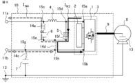
- 4 is a diagram illustrating propagation of common mode noise current in the power converter according to Embodiment 1;
- FIG. FIG. 4 is a schematic diagram showing an example of a case where mode conversion does not occur in electromagnetic noise;
- FIG. 2 is a schematic diagram showing an example of mode conversion in electromagnetic noise;
- 3 is a circuit diagram showing a configuration of a power conversion device of Comparative Example 1;
- FIG. 3 is a circuit diagram showing a configuration of a power conversion device of Comparative Example 1;
- FIG. 3 is a circuit diagram showing the configuration of a power conversion device of Comparative Example 2;
- FIG. 3 is a circuit diagram showing the configuration of a power conversion device of Comparative Example 2;
- FIG. 4 is another circuit diagram of the power converter according to Embodiment 1.
- FIG. FIG. 7 is a circuit diagram showing the configuration of a power conversion device according to Embodiment 2;
- FIG. 10 is a circuit diagram showing the configuration of a power conversion device according to Embodiment 3;
- FIG. 11 is a circuit diagram showing the configuration of a power conversion device according to Embodiment 4;
- FIG. 11 is a circuit diagram showing the configuration of a power conversion device according to Embodiment 5;
- FIG. 1 is a circuit diagram of a power converter according to Embodiment 1.
- the power converter 10 converts any DC voltage input from the input terminals 11 a and 11 b into any AC voltage or DC voltage to drive the load 8 .
- the output is AC voltage, it functions as a DC-AC converter (inverter), and when the output is DC voltage, it functions as a DC-DC converter (converter).
- the power conversion device 10 includes a switching element 1, a control unit 2 that supplies switching signals for opening and closing the switching element 1, a choke coil 4, a first line capacitor 5, a second line capacitor 6, and a ground capacitor 7. It is A drive unit 3 is composed of the switching element 1 and the control unit 2 . The drive unit 3 and the load 8 are connected by a connection wiring 9, and the load 8 is driven by arbitrary AC power or DC power output from the drive unit.
- Parasitic inductances 14a and 14c are present in the second line-to-line capacitor 6 and the line-to-ground capacitor 7, respectively. In the figure, the parasitic inductance is indicated by a dashed line. Parasitic inductance also exists in the first line-to-line capacitor 5 or other connection wiring, but only the portions necessary for explaining the effects of the present embodiment are shown in the figure.
- the plus side terminal is serially connected to the connection terminal 15c of the second line capacitor, the choke coil 4, the connection terminal 15d of the first line capacitor, and the connection terminal 15a of the drive unit 3 in order from the input terminal 11a.
- An electric circuit is formed.
- the terminals on the negative side are the connection terminal 15g of the capacitor to ground 7, the connection terminal 15e of the second capacitor between lines, the connection terminal 15f of the first capacitor between lines, and the connection terminal 15b of the driving section 3 in this order from the input terminal 11b. , are connected in series to form an electric path.
- the other terminal of capacitor 7 to ground is connected to ground potential 12 .
- the input power is DC power, but the input power is AC power, and the AC power is converted into DC power using a rectifier circuit and applied to the input terminals 11a and 11b.
- the choke coil 4 is connected to the positive side and one terminal of the capacitor to ground 7 is connected to the negative side.
- the connection terminal 15g may be configured to be connected to the positive side.
- the capacitor to ground 7 is arranged between the input terminal 11b and the connection terminal 15e of the second line capacitor. and the connection terminal 15f of the first line capacitor, or between the connection terminal 15f of the first line capacitor and the connection terminal 15b of the driving section 3.
- one drive unit 3 drives one load 8, but this is not the only option, and a plurality of drive units may drive multiple loads.
- FIG. 2 shows an example of a circuit diagram when the drive unit 3 is an inverter.
- the inverter 201 is connected from the input terminals 11a and 11b to the connection terminals 15a and 15b via the connections described above, and has switching elements 1a, 1b and 1c for switching arbitrary DC power input to the input terminals 11a and 11b.
- 1d, 1e, and 1f are controlled by the control unit 2 to convert into any three-phase AC power consisting of U-phase, V-phase, and W-phase, and output from output terminals 101a, 101b, and 101c.
- the output terminals 101 a , 101 b , 101 c of the inverter 201 and the input terminals 102 a , 102 b , 102 c of the load 8 are connected by the connection wiring 9 .
- the DC power is converted into arbitrary three-phase AC power consisting of U-phase, V-phase, and W-phase, and the load 8 is driven.
- the switching elements 1a, 1b, 1c, 1d, 1e, and 1f are MOSFETs (Metal-Oxide-Semiconductor Field-Effect-Transistors), but the present invention is not limited to this. It is good also as a switching element other than MOSFET.
- MOSFETs Metal-Oxide-Semiconductor Field-Effect-Transistors
- FIG. 3 shows an example of a circuit diagram when the drive unit 3 is a converter.
- the positive side terminal 103a is connected to the connection terminal 15a in FIG. 1 with the high voltage V HIGH side as an input
- the negative side terminal 103b is connected to the connection terminal 15b in FIG.
- the side terminal 104b is connected to the connection wiring 9 in FIG. In this case, it functions as a step-down converter that steps down the DC voltage.
- the positive terminal 104a is connected to the connection terminal 15a in FIG. 1 with the low voltage V LOW side as an input
- the negative terminal 104b is connected to the connection terminal 15b in FIG. 103a
- the negative terminal 103b are connected to the connection wiring 9 in FIG. 1, it functions as a boost converter for boosting the DC voltage.
- the converter 202 opens and closes the switching elements 1g and 1h, the high-voltage side smoothing capacitor 203a, the low-voltage side smoothing capacitor 203b, the reactor 204, and the switching elements 1g and 1h, and supplies switching signals for controlling the load 8 in FIG. It is composed of a control unit 2 that
- the plus side terminals are, in order from the plus side terminal 103a on the high voltage V HIGH side, the plus side terminal of the smoothing capacitor 203a, the plus side terminals of the switching elements 1g and 1h, the reactor 204, the plus side terminal of the smoothing capacitor 203b, and the low voltage. It is connected in series with the plus side terminal 104a on the V LOW side.
- the negative terminals are, in order from the negative terminal 103b on the high voltage V HIGH side, the negative terminal of the smoothing capacitor 203a, the negative terminal of the switching element 1h, the negative terminal of the smoothing capacitor 203b, and the negative terminal on the low voltage V LOW side. It is connected in series with the side terminal 104b.
- the common mode noise current IN0 propagates from the housing to the outside of the device via the impedance to ground 13 of the load.
- the housing potential ground potential 12
- the bypassed common mode noise current IN0 is fed back to the switching element 1 via the connection terminals 15a and 15b.
- the common mode noise current IN0 When the common mode noise current IN0 is fed back to the switching element 1 via the connection terminal 15a, the common mode noise current INO bypassed from the ground potential flows through the first line capacitor 5 as shown in FIG. propagates from the negative side to the positive side.
- the common mode noise current IN0 is fed back to the switching element 1 via the connection terminal 15b, the common mode noise current IN0 bypassed from the ground potential propagates on the negative side as it is, as shown in FIG.
- FIG. 5 When a common mode noise voltage V C is applied between the midpoint of the input terminal 11a and the input terminal 11b and the ground potential 12, a common mode noise current I C flows, and the positive side and the negative side are I 1C and I 2C , respectively. divert.
- the common mode noise current is I1C ⁇ I2C .
- a differential mode noise voltage VD is applied between the plus side and the minus side, thereby superimposing a differential mode noise current ID .
- FIG. 7 shows Comparative Example 1 of the present embodiment.
- ground capacitors 7a and 7b are provided on the positive side and the negative side, respectively.
- the common mode noise current IN0 that propagates from the housing to the outside of the device via the impedance to ground 13 of the load is bypassed by the common mode noise current IN1 that is bypassed by the capacitor to ground 7a and by the capacitor to ground 7b.
- shunted to the common mode noise current IN2 Since the choke coil 4 is a high impedance element and the second line capacitor 6 is a low impedance element, the common mode noise current IN1 propagates through the second line capacitor 6 to the negative side.
- the combined impedance in the propagation path of the common mode noise current IN1 is larger than the combined impedance in the propagation path of the common mode noise current IN2 by the impedance of the second line-to-line capacitor 6, and the impedance of the propagation path increases. An imbalance will occur, and mode conversion of electromagnetic noise will occur.
- the impedance of the second line-to-line capacitor 6 includes not only the electrostatic capacity but also the influence of the parasitic inductance 14a caused by the element, wiring, bus bar, and cable. Further, when the impedances of the capacitors 7a and 7b to ground are different, the combined impedance in the propagation paths of the common mode noise currents I N1 and I N2 is further unbalanced.
- the impedance of the capacitors 7a and 7b to ground includes not only the electrostatic capacitance but also the effects of parasitic inductances 14b and 14c caused by elements, wiring, bus bars and cables.
- Comparative Example 1 in order to eliminate the influence of such impedance imbalance, as shown in FIG. It balances the impedance on the side and suppresses the mode conversion of electromagnetic noise.
- the choke coil 4 is arranged on one of the plus side and the minus side, and the capacitor to ground 7 is between the other of the plus side and the minus side and the ground potential. are placed in As a result, the common mode noise current IN0 is bypassed to the negative side by the capacitor to ground, so that the electromagnetic noise mode conversion in FIG. can be suppressed.
- connection terminal 15f of the first line capacitor 5 and the connection terminal 15e of the second line capacitor 6 are connected to the negative side through a common connection terminal 15h.
- a part of the differential mode noise current IN3 bypassed by the first line capacitor 5 is shunted to become a noise current IN4 , which is bypassed to the outside of the power converter 10 by the second line capacitor 6.
- connection terminal 15f of the first line capacitor 5 and the connection terminal 15e of the second line capacitor 6 are common on the negative side where the choke coil 4 is not arranged. are connected individually without being merged.
- the connection terminal 15f of the first line capacitor 5 and the connection terminal 15e of the second line capacitor 6 are not shared, and power conversion is performed. Differential mode noise currents bypassed outside of device 10 can be reduced.
- the side on which the choke coil 4 is not arranged is the negative side in FIG.
- connection terminal 15f of the first line capacitor 5, the connection terminal 15e of the second line capacitor 6, and the connection terminal 15g of the capacitor to ground are common connection terminals.
- This is an example of a power converter connected to the negative side at 15h.
- part of the differential mode noise current IN3 bypassed by the first line capacitor 5 flows through the parasitic inductance 14d at the common connection terminal, causing voltage fluctuations in the parasitic inductance 14d.
- the common mode noise current IN5 is newly superimposed.
- connection terminal 15g on the negative side of the capacitor to ground 7 is shared with the connection terminal 15f of the first line capacitor 5 and the connection terminal 15e of the second line capacitor 6. are configured to be connected individually.
- the connection terminal 15g on the negative side of the capacitor to ground 7 is not shared with the connection terminal 15f of the first line capacitor 5 and the connection terminal 15e of the second line capacitor 6, but is individually connected.
- new superimposed common mode noise current can be reduced.
- the connection terminal of the capacitor 7 to ground is connected to the positive side, the connection terminal of the first line capacitor 5 and the connection terminal of the second line capacitor 6 are not shared by the same configuration. A similar effect can be obtained by connecting them individually.
- the side on which the choke coil 4 is not arranged is the negative side in FIG.
- FIG. 11 shows an example in which the choke coil 4 is arranged on the plus side, the capacitor to ground 7 is arranged between the minus side and the ground potential, and the minus side is connected including a heat sink in the power converter shown in FIG. is shown. Even with such a structure, the same effect as described above can be obtained.
- the negative side includes the heat sink 16, but the configuration is not limited to this, and may include a metal housing.
- the connection terminals of the first line capacitor 5 and the second line capacitor 6 are shared.
- the ground capacitor 7 between the other of the plus side and the minus side and the ground potential, it is possible to reduce the imbalance of impedance against common mode noise. Mode conversion of electromagnetic noise generated from the power converter can be suppressed without adding an element.
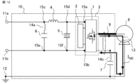
- FIG. 12 shows an example of the power converter shown in FIG. 1 in which the ground capacitor 7 is arranged close to the connection wiring 9 . Even with such a structure, it is possible to obtain the same effects as those of the power converter shown in the first embodiment. Further, the directions of the common mode noise current IN0 are opposite to each other between the connection wiring 9 and the capacitor to ground 7, so that the parasitic inductance 14c of the capacitor to ground 7 is reduced. As a result, the impedance of the capacitor 7 to ground is further reduced, thereby further improving the bypass effect of the common mode noise current IN0 .
- the impedance of the ground capacitor 7 includes not only the element itself, but also wiring, bus bars, and cables for connecting the ground capacitor 7 to the ground potential, plus side or minus side.
- the connection wiring 9, which is arranged close to the ground, and the wiring, bus bar, and cable for connecting the capacitor 7 to ground may not only be arranged close to each other, but may also be twisted with each other.
- FIG. 13 shows an example of a power converter in which the connection wiring 9 is electrically shielded by the shield part 17 in the power converter shown in FIG.
- the choke coil 4 when the choke coil 4 is arranged on the plus side, by arranging the ground capacitor 7 between the minus side and the ground potential, impedance imbalance against common mode noise can be reduced. is possible, and in addition to being able to suppress mode conversion of electromagnetic noise generated from the power converter without adding an element for impedance balancing, radiation noise generated from the connection wiring 9 can be reduced. can.
- a similar effect can be obtained by wiring the ground capacitor 7 to the positive side. Further, even if the choke coil 4 is arranged on the negative side, the same effect can be obtained with the same configuration.
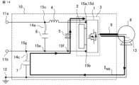
- FIG. 14 shows an example in which the connection terminal 15d of the first line capacitor 5 is directly connected to the connection terminal 15a of the driving section 3 in the power converter shown in FIG. Even with such a structure, it is possible to obtain the same effects as those of the power converter shown in the first embodiment. Moreover, the parasitic inductance between the connection terminal 15d of the first line capacitor and the connection terminal 15a of the driving section 3 is reduced. As a result, the impedance between the connection terminal 15d of the first line-to-line capacitor and the connection terminal 15a of the drive section 3 can be further reduced, thereby further improving the bypass effect of the noise current IN0 .
- FIG. 15 shows an example in which an LC filter 20 comprising a choke coil 18 and a third line-to-line capacitor 19 is added to the power converter shown in FIG.
- the third line capacitor 19 is connected in order from the input terminal 11a between the input terminal 11a and the connection terminal 15c of the second line capacitor in the preceding stage of the second line capacitor 6.
- a terminal 15i, a choke coil 18, and a connection terminal 15c of the second line capacitor are connected in series.
- the connection terminal 15j of the third line-to-line capacitor 19 is connected in series between the connection terminal 15g of the line-to-ground capacitor 7 and the connection terminal 15e of the second line-to-line capacitor.
- connection terminal 15g on the negative side of the capacitor to ground 7 is connected to the connection terminal 15f of the first line capacitor 5, the connection terminal 15e of the second line capacitor 6, and the connection terminal 15j of the third line capacitor 19. are individually connected without being shared.
- the differential mode noise current bypassed to the outside of the power converter 10 and the common mode noise current newly superimposed can be reduced.
- the choke coil 18 and the third line-to-line capacitor 19 can further improve the effect of reducing differential mode noise generated from the driving section 3 .
- a similar effect can be obtained by wiring the ground capacitor 7 to the positive side.
- one LC filter 20 is added, but this is not the only option, and a plurality of LC filters may be added.
Landscapes
- Engineering & Computer Science (AREA)
- Power Engineering (AREA)
- Physics & Mathematics (AREA)
- Electromagnetism (AREA)
- Power Conversion In General (AREA)
Priority Applications (4)
| Application Number | Priority Date | Filing Date | Title |
|---|---|---|---|
| EP21963214.8A EP4429096A4 (en) | 2021-11-04 | 2021-11-04 | POWER CONVERTER |
| PCT/JP2021/040569 WO2023079617A1 (ja) | 2021-11-04 | 2021-11-04 | 電力変換装置 |
| JP2022515494A JPWO2023079617A1 (https=) | 2021-11-04 | 2021-11-04 | |
| US18/702,817 US20250233514A1 (en) | 2021-11-04 | 2021-11-04 | Power conversion device |
Applications Claiming Priority (1)
| Application Number | Priority Date | Filing Date | Title |
|---|---|---|---|
| PCT/JP2021/040569 WO2023079617A1 (ja) | 2021-11-04 | 2021-11-04 | 電力変換装置 |
Publications (1)
| Publication Number | Publication Date |
|---|---|
| WO2023079617A1 true WO2023079617A1 (ja) | 2023-05-11 |
Family
ID=86240748
Family Applications (1)
| Application Number | Title | Priority Date | Filing Date |
|---|---|---|---|
| PCT/JP2021/040569 Ceased WO2023079617A1 (ja) | 2021-11-04 | 2021-11-04 | 電力変換装置 |
Country Status (4)
| Country | Link |
|---|---|
| US (1) | US20250233514A1 (https=) |
| EP (1) | EP4429096A4 (https=) |
| JP (1) | JPWO2023079617A1 (https=) |
| WO (1) | WO2023079617A1 (https=) |
Citations (6)
| Publication number | Priority date | Publication date | Assignee | Title |
|---|---|---|---|---|
| JPH09285000A (ja) * | 1996-04-10 | 1997-10-31 | Ricoh Co Ltd | スイッチングレギュレータ |
| JP2001178127A (ja) * | 1999-12-13 | 2001-06-29 | Sony Corp | スイッチング電源回路 |
| JP2006296067A (ja) * | 2005-04-08 | 2006-10-26 | Matsushita Electric Ind Co Ltd | 空気調和機 |
| JP2016010308A (ja) * | 2014-06-26 | 2016-01-18 | 富士電機株式会社 | 電力変換装置 |
| JP6045664B1 (ja) | 2015-08-20 | 2016-12-14 | 三菱電機株式会社 | 電力変換装置 |
| JP2019047541A (ja) * | 2017-08-29 | 2019-03-22 | ダイキン工業株式会社 | 電力変換システム |
Family Cites Families (18)
| Publication number | Priority date | Publication date | Assignee | Title |
|---|---|---|---|---|
| JPH05219758A (ja) * | 1992-02-03 | 1993-08-27 | Fuji Electric Co Ltd | 電力変換装置のノイズ防止装置 |
| JP2002335688A (ja) * | 2001-05-09 | 2002-11-22 | Mitsubishi Electric Corp | 電源回路 |
| JP4032723B2 (ja) * | 2001-12-06 | 2008-01-16 | 松下電器産業株式会社 | 空調装置 |
| JP5235820B2 (ja) * | 2009-08-17 | 2013-07-10 | 株式会社日立産機システム | 電力変換装置 |
| JP5721772B2 (ja) * | 2013-05-16 | 2015-05-20 | 三菱電機株式会社 | 電力変換装置 |
| EP3273585B1 (en) * | 2015-03-16 | 2023-04-26 | Mitsubishi Electric Corporation | Power circuit device |
| JP2017069675A (ja) * | 2015-09-29 | 2017-04-06 | 北川工業株式会社 | ノイズ低減装置 |
| JP6643972B2 (ja) * | 2016-12-13 | 2020-02-12 | 日立オートモティブシステムズ株式会社 | バスバ構造およびそれを用いた電力変換装置 |
| JP2019102477A (ja) * | 2017-11-28 | 2019-06-24 | 株式会社ジェイテクト | 回路モジュール |
| US10784678B1 (en) * | 2018-01-26 | 2020-09-22 | Universal Lighting Technologies, Inc. | Damped PI-type filter Y-type capacitance network for radiated and conducted emission |
| US10554122B1 (en) * | 2018-06-29 | 2020-02-04 | Universal Lighting Technologies, Inc. | Low loss voltage feedback method for power factor correction circuits |
| JP7009325B2 (ja) * | 2018-07-09 | 2022-01-25 | サンデン・オートモーティブコンポーネント株式会社 | スイッチング電源装置及びそれを備えた車載用電動コンプレッサ |
| JP7152296B2 (ja) * | 2018-12-20 | 2022-10-12 | 株式会社日立製作所 | 電力変換装置、及び高電圧ノイズフィルタ |
| JP7135949B2 (ja) * | 2019-03-14 | 2022-09-13 | 株式会社デンソー | 電力変換装置 |
| EP3952091A4 (en) * | 2019-03-25 | 2022-05-04 | Panasonic Intellectual Property Management Co., Ltd. | SWITCHING POWER SUPPLY DEVICE |
| CN210867501U (zh) * | 2019-10-11 | 2020-06-26 | 博世华域转向系统有限公司 | 一种电动助力转向系统控制器的电源接口滤波电路 |
| DE112020005305T5 (de) * | 2019-12-17 | 2022-09-15 | Murata Manufacturing Co., Ltd. | Elektronische schaltung |
| US12009734B2 (en) * | 2020-04-20 | 2024-06-11 | Mitsubishi Electric Corporation | Power conversion device and air conditioner |
-
2021
- 2021-11-04 JP JP2022515494A patent/JPWO2023079617A1/ja active Pending
- 2021-11-04 EP EP21963214.8A patent/EP4429096A4/en not_active Withdrawn
- 2021-11-04 US US18/702,817 patent/US20250233514A1/en active Pending
- 2021-11-04 WO PCT/JP2021/040569 patent/WO2023079617A1/ja not_active Ceased
Patent Citations (6)
| Publication number | Priority date | Publication date | Assignee | Title |
|---|---|---|---|---|
| JPH09285000A (ja) * | 1996-04-10 | 1997-10-31 | Ricoh Co Ltd | スイッチングレギュレータ |
| JP2001178127A (ja) * | 1999-12-13 | 2001-06-29 | Sony Corp | スイッチング電源回路 |
| JP2006296067A (ja) * | 2005-04-08 | 2006-10-26 | Matsushita Electric Ind Co Ltd | 空気調和機 |
| JP2016010308A (ja) * | 2014-06-26 | 2016-01-18 | 富士電機株式会社 | 電力変換装置 |
| JP6045664B1 (ja) | 2015-08-20 | 2016-12-14 | 三菱電機株式会社 | 電力変換装置 |
| JP2019047541A (ja) * | 2017-08-29 | 2019-03-22 | ダイキン工業株式会社 | 電力変換システム |
Non-Patent Citations (1)
| Title |
|---|
| See also references of EP4429096A4 |
Also Published As
| Publication number | Publication date |
|---|---|
| JPWO2023079617A1 (https=) | 2023-05-11 |
| US20250233514A1 (en) | 2025-07-17 |
| EP4429096A1 (en) | 2024-09-11 |
| EP4429096A4 (en) | 2024-12-25 |
Similar Documents
| Publication | Publication Date | Title |
|---|---|---|
| US8138694B2 (en) | Bidirectional buck-boost power converters | |
| US7880088B2 (en) | Power electronic switching device with laminated bus | |
| US11239766B2 (en) | Flying capacitor circuit, circuit module and power conversion apparatus | |
| KR100544758B1 (ko) | 교류 라인에 연결된 능동 공통 모드 필터 | |
| US11070163B2 (en) | Driving power supply device | |
| CN103650316A (zh) | 电力变换装置 | |
| US10910944B2 (en) | Voltage converter, electric drive system and method for reducing interference voltages | |
| JP2017146154A (ja) | 電流検出装置および半導体装置 | |
| US11398772B2 (en) | Circuit device for reducing common-mode interference of a power converter | |
| EP3955453B1 (en) | Power conversion device | |
| US11050358B2 (en) | Power module with built-in drive circuit | |
| JPH10135681A (ja) | 可変速駆動装置 | |
| US11431239B2 (en) | Power converter | |
| US4617621A (en) | Inverters with reduced distributed inductance | |
| JP2006020389A (ja) | ノイズフィルタおよびそれを搭載したモータ駆動装置 | |
| JP2006020389A5 (https=) | ||
| JP6720601B2 (ja) | 電力変換装置 | |
| WO2023079617A1 (ja) | 電力変換装置 | |
| JP7716346B2 (ja) | 半導体装置および半導体装置を備えたインバータ | |
| JP3315303B2 (ja) | 電動機制御装置 | |
| WO2018100645A1 (ja) | 電力変換装置 | |
| JP7275397B1 (ja) | バスバーモジュール及び電力変換システム | |
| JPS59153476A (ja) | インバ−タ装置 | |
| JP7511669B2 (ja) | ノイズフィルタ | |
| CN1245297C (zh) | 电动车控制装置 |
Legal Events
| Date | Code | Title | Description |
|---|---|---|---|
| WWE | Wipo information: entry into national phase |
Ref document number: 2022515494 Country of ref document: JP |
|
| 121 | Ep: the epo has been informed by wipo that ep was designated in this application |
Ref document number: 21963214 Country of ref document: EP Kind code of ref document: A1 |
|
| WWE | Wipo information: entry into national phase |
Ref document number: 18702817 Country of ref document: US |
|
| WWE | Wipo information: entry into national phase |
Ref document number: 2021963214 Country of ref document: EP |
|
| NENP | Non-entry into the national phase |
Ref country code: DE |
|
| ENP | Entry into the national phase |
Ref document number: 2021963214 Country of ref document: EP Effective date: 20240604 |
|
| WWP | Wipo information: published in national office |
Ref document number: 18702817 Country of ref document: US |
|
| WWW | Wipo information: withdrawn in national office |
Ref document number: 2021963214 Country of ref document: EP |