WO2023074836A1 - β-Ga2O3/β-Ga2O3積層体の製造方法 - Google Patents
β-Ga2O3/β-Ga2O3積層体の製造方法 Download PDFInfo
- Publication number
- WO2023074836A1 WO2023074836A1 PCT/JP2022/040309 JP2022040309W WO2023074836A1 WO 2023074836 A1 WO2023074836 A1 WO 2023074836A1 JP 2022040309 W JP2022040309 W JP 2022040309W WO 2023074836 A1 WO2023074836 A1 WO 2023074836A1
- Authority
- WO
- WIPO (PCT)
- Prior art keywords
- pbo
- mol
- laminate
- growth
- substrate
- Prior art date
- Legal status (The legal status is an assumption and is not a legal conclusion. Google has not performed a legal analysis and makes no representation as to the accuracy of the status listed.)
- Ceased
Links
Images


Classifications
-
- C—CHEMISTRY; METALLURGY
- C30—CRYSTAL GROWTH
- C30B—SINGLE-CRYSTAL GROWTH; UNIDIRECTIONAL SOLIDIFICATION OF EUTECTIC MATERIAL OR UNIDIRECTIONAL DEMIXING OF EUTECTOID MATERIAL; REFINING BY ZONE-MELTING OF MATERIAL; PRODUCTION OF A HOMOGENEOUS POLYCRYSTALLINE MATERIAL WITH DEFINED STRUCTURE; SINGLE CRYSTALS OR HOMOGENEOUS POLYCRYSTALLINE MATERIAL WITH DEFINED STRUCTURE; AFTER-TREATMENT OF SINGLE CRYSTALS OR A HOMOGENEOUS POLYCRYSTALLINE MATERIAL WITH DEFINED STRUCTURE; APPARATUS THEREFOR
- C30B29/00—Single crystals or homogeneous polycrystalline material with defined structure characterised by the material or by their shape
- C30B29/10—Inorganic compounds or compositions
- C30B29/16—Oxides
-
- C—CHEMISTRY; METALLURGY
- C30—CRYSTAL GROWTH
- C30B—SINGLE-CRYSTAL GROWTH; UNIDIRECTIONAL SOLIDIFICATION OF EUTECTIC MATERIAL OR UNIDIRECTIONAL DEMIXING OF EUTECTOID MATERIAL; REFINING BY ZONE-MELTING OF MATERIAL; PRODUCTION OF A HOMOGENEOUS POLYCRYSTALLINE MATERIAL WITH DEFINED STRUCTURE; SINGLE CRYSTALS OR HOMOGENEOUS POLYCRYSTALLINE MATERIAL WITH DEFINED STRUCTURE; AFTER-TREATMENT OF SINGLE CRYSTALS OR A HOMOGENEOUS POLYCRYSTALLINE MATERIAL WITH DEFINED STRUCTURE; APPARATUS THEREFOR
- C30B19/00—Liquid-phase epitaxial-layer growth
- C30B19/12—Liquid-phase epitaxial-layer growth characterised by the substrate
-
- C—CHEMISTRY; METALLURGY
- C30—CRYSTAL GROWTH
- C30B—SINGLE-CRYSTAL GROWTH; UNIDIRECTIONAL SOLIDIFICATION OF EUTECTIC MATERIAL OR UNIDIRECTIONAL DEMIXING OF EUTECTOID MATERIAL; REFINING BY ZONE-MELTING OF MATERIAL; PRODUCTION OF A HOMOGENEOUS POLYCRYSTALLINE MATERIAL WITH DEFINED STRUCTURE; SINGLE CRYSTALS OR HOMOGENEOUS POLYCRYSTALLINE MATERIAL WITH DEFINED STRUCTURE; AFTER-TREATMENT OF SINGLE CRYSTALS OR A HOMOGENEOUS POLYCRYSTALLINE MATERIAL WITH DEFINED STRUCTURE; APPARATUS THEREFOR
- C30B19/00—Liquid-phase epitaxial-layer growth
- C30B19/02—Liquid-phase epitaxial-layer growth using molten solvents, e.g. flux
-
- H—ELECTRICITY
- H10—SEMICONDUCTOR DEVICES; ELECTRIC SOLID-STATE DEVICES NOT OTHERWISE PROVIDED FOR
- H10P—GENERIC PROCESSES OR APPARATUS FOR THE MANUFACTURE OR TREATMENT OF DEVICES COVERED BY CLASS H10
- H10P14/00—Formation of materials, e.g. in the shape of layers or pillars
- H10P14/20—Formation of materials, e.g. in the shape of layers or pillars of semiconductor materials
- H10P14/26—Formation of materials, e.g. in the shape of layers or pillars of semiconductor materials using liquid deposition
- H10P14/263—Formation of materials, e.g. in the shape of layers or pillars of semiconductor materials using liquid deposition using melted materials
-
- H—ELECTRICITY
- H10—SEMICONDUCTOR DEVICES; ELECTRIC SOLID-STATE DEVICES NOT OTHERWISE PROVIDED FOR
- H10P—GENERIC PROCESSES OR APPARATUS FOR THE MANUFACTURE OR TREATMENT OF DEVICES COVERED BY CLASS H10
- H10P14/00—Formation of materials, e.g. in the shape of layers or pillars
- H10P14/20—Formation of materials, e.g. in the shape of layers or pillars of semiconductor materials
- H10P14/26—Formation of materials, e.g. in the shape of layers or pillars of semiconductor materials using liquid deposition
- H10P14/265—Formation of materials, e.g. in the shape of layers or pillars of semiconductor materials using liquid deposition using solutions
-
- H—ELECTRICITY
- H10—SEMICONDUCTOR DEVICES; ELECTRIC SOLID-STATE DEVICES NOT OTHERWISE PROVIDED FOR
- H10P—GENERIC PROCESSES OR APPARATUS FOR THE MANUFACTURE OR TREATMENT OF DEVICES COVERED BY CLASS H10
- H10P14/00—Formation of materials, e.g. in the shape of layers or pillars
- H10P14/20—Formation of materials, e.g. in the shape of layers or pillars of semiconductor materials
- H10P14/29—Formation of materials, e.g. in the shape of layers or pillars of semiconductor materials characterised by the substrates
- H10P14/2901—Materials
- H10P14/2918—Materials being semiconductor metal oxides
-
- H—ELECTRICITY
- H10—SEMICONDUCTOR DEVICES; ELECTRIC SOLID-STATE DEVICES NOT OTHERWISE PROVIDED FOR
- H10P—GENERIC PROCESSES OR APPARATUS FOR THE MANUFACTURE OR TREATMENT OF DEVICES COVERED BY CLASS H10
- H10P14/00—Formation of materials, e.g. in the shape of layers or pillars
- H10P14/20—Formation of materials, e.g. in the shape of layers or pillars of semiconductor materials
- H10P14/34—Deposited materials, e.g. layers
- H10P14/3402—Deposited materials, e.g. layers characterised by the chemical composition
- H10P14/3434—Deposited materials, e.g. layers characterised by the chemical composition being oxide semiconductor materials
-
- H—ELECTRICITY
- H10—SEMICONDUCTOR DEVICES; ELECTRIC SOLID-STATE DEVICES NOT OTHERWISE PROVIDED FOR
- H10P—GENERIC PROCESSES OR APPARATUS FOR THE MANUFACTURE OR TREATMENT OF DEVICES COVERED BY CLASS H10
- H10P14/00—Formation of materials, e.g. in the shape of layers or pillars
- H10P14/20—Formation of materials, e.g. in the shape of layers or pillars of semiconductor materials
- H10P14/34—Deposited materials, e.g. layers
- H10P14/3438—Doping during depositing
- H10P14/3441—Conductivity type
- H10P14/3442—N-type
-
- H—ELECTRICITY
- H10—SEMICONDUCTOR DEVICES; ELECTRIC SOLID-STATE DEVICES NOT OTHERWISE PROVIDED FOR
- H10P—GENERIC PROCESSES OR APPARATUS FOR THE MANUFACTURE OR TREATMENT OF DEVICES COVERED BY CLASS H10
- H10P14/00—Formation of materials, e.g. in the shape of layers or pillars
- H10P14/20—Formation of materials, e.g. in the shape of layers or pillars of semiconductor materials
- H10P14/34—Deposited materials, e.g. layers
- H10P14/3438—Doping during depositing
- H10P14/3441—Conductivity type
- H10P14/3444—P-type
-
- H—ELECTRICITY
- H10—SEMICONDUCTOR DEVICES; ELECTRIC SOLID-STATE DEVICES NOT OTHERWISE PROVIDED FOR
- H10P—GENERIC PROCESSES OR APPARATUS FOR THE MANUFACTURE OR TREATMENT OF DEVICES COVERED BY CLASS H10
- H10P14/00—Formation of materials, e.g. in the shape of layers or pillars
- H10P14/20—Formation of materials, e.g. in the shape of layers or pillars of semiconductor materials
- H10P14/34—Deposited materials, e.g. layers
- H10P14/3438—Doping during depositing
- H10P14/3441—Conductivity type
- H10P14/3446—Transition metal elements; Rare earth elements
-
- H—ELECTRICITY
- H10—SEMICONDUCTOR DEVICES; ELECTRIC SOLID-STATE DEVICES NOT OTHERWISE PROVIDED FOR
- H10P—GENERIC PROCESSES OR APPARATUS FOR THE MANUFACTURE OR TREATMENT OF DEVICES COVERED BY CLASS H10
- H10P14/00—Formation of materials, e.g. in the shape of layers or pillars
- H10P14/60—Formation of materials, e.g. in the shape of layers or pillars of insulating materials
- H10P14/63—Formation of materials, e.g. in the shape of layers or pillars of insulating materials characterised by the formation processes
- H10P14/6302—Non-deposition formation processes
-
- H—ELECTRICITY
- H10—SEMICONDUCTOR DEVICES; ELECTRIC SOLID-STATE DEVICES NOT OTHERWISE PROVIDED FOR
- H10P—GENERIC PROCESSES OR APPARATUS FOR THE MANUFACTURE OR TREATMENT OF DEVICES COVERED BY CLASS H10
- H10P14/00—Formation of materials, e.g. in the shape of layers or pillars
- H10P14/60—Formation of materials, e.g. in the shape of layers or pillars of insulating materials
- H10P14/69—Inorganic materials
- H10P14/692—Inorganic materials composed of oxides, glassy oxides or oxide-based glasses
- H10P14/6938—Inorganic materials composed of oxides, glassy oxides or oxide-based glasses the material containing at least one metal element, e.g. metal oxides, metal oxynitrides or metal oxycarbides
- H10P14/6939—Inorganic materials composed of oxides, glassy oxides or oxide-based glasses the material containing at least one metal element, e.g. metal oxides, metal oxynitrides or metal oxycarbides characterised by the metal
-
- H—ELECTRICITY
- H10—SEMICONDUCTOR DEVICES; ELECTRIC SOLID-STATE DEVICES NOT OTHERWISE PROVIDED FOR
- H10P—GENERIC PROCESSES OR APPARATUS FOR THE MANUFACTURE OR TREATMENT OF DEVICES COVERED BY CLASS H10
- H10P14/00—Formation of materials, e.g. in the shape of layers or pillars
- H10P14/20—Formation of materials, e.g. in the shape of layers or pillars of semiconductor materials
- H10P14/32—Formation of materials, e.g. in the shape of layers or pillars of semiconductor materials characterised by intermediate layers between substrates and deposited layers
- H10P14/3202—Materials thereof
- H10P14/3234—Materials thereof being oxide semiconducting materials
-
- Y—GENERAL TAGGING OF NEW TECHNOLOGICAL DEVELOPMENTS; GENERAL TAGGING OF CROSS-SECTIONAL TECHNOLOGIES SPANNING OVER SEVERAL SECTIONS OF THE IPC; TECHNICAL SUBJECTS COVERED BY FORMER USPC CROSS-REFERENCE ART COLLECTIONS [XRACs] AND DIGESTS
- Y02—TECHNOLOGIES OR APPLICATIONS FOR MITIGATION OR ADAPTATION AGAINST CLIMATE CHANGE
- Y02P—CLIMATE CHANGE MITIGATION TECHNOLOGIES IN THE PRODUCTION OR PROCESSING OF GOODS
- Y02P70/00—Climate change mitigation technologies in the production process for final industrial or consumer products
- Y02P70/50—Manufacturing or production processes characterised by the final manufactured product
Definitions
- the present invention relates to a method for producing a ⁇ -Ga 2 O 3 / ⁇ -Ga 2 O 3 laminate and the laminate obtained by the method.
- Power devices are one of the key devices for improving the efficiency of power usage for the realization of a low-carbon society. ing.
- energy loss due to resistance when current flows through the element and wasteful current generation due to the recovery process of the charge distribution in the element that occurs at the moment when the voltage applied to the element is switched cannot be avoided.
- These loss ratios vary depending on power and frequency, but generally range from several percent to ten and several percent.
- the device structure of conventional power semiconductors using Si has been devised, but Si is approaching its physical limit, and it is difficult to improve efficiency further. Therefore, SiC and GaN are being developed as power device materials to replace Si.
- SiC has a bandgap of 3.3 eV and GaN has a bandgap of 3.4 eV, which are wider bandgap materials than Si's 1.1 eV.
- a material with a wider bandgap has a higher dielectric breakdown voltage, which indicates the electric field at the limit (avalanche breakdown) that prevents charges from leaking into the semiconductor, and a device structure capable of withstanding a higher voltage can be adopted.
- ⁇ -Ga 2 O 3 is a type of oxide semiconductor, and has been applied to transparent conductive substrates for GaN-based LEDs, solar blind ultraviolet detectors, etc. In recent years, it has also attracted attention as a power device material. It is expected to realize a high-voltage and high-efficiency power semiconductor that surpasses SiC and GaN. This is because the bandgap of ⁇ -Ga 2 O 3 is expected to be 4.5 to 4.9 eV, which is wider than that of SiC and GaN. Another advantage of ⁇ -Ga 2 O 3 over SiC and GaN is that crystal growth from a melt is possible. SiC and GaN are difficult to crystallize from a melt, and there is a problem that the substrate is expensive.
- ⁇ -Ga 2 O 3 has a melting point at normal pressure and is capable of bulk crystal growth, and is being researched and developed by the EFG (Edge-Defined Film-fed Growth) method and the vertical Bridgman method.
- EFG Edge-Defined Film-fed Growth
- vertical Bridgman method For the former growth method, substrates of 2 to 4 inches are commercially available, and for the latter growth method, a 4-inch substrate is under development.
- ⁇ -Ga 2 O 3 epitaxial layer
- the thickness of the epitaxial layer is required to be several ⁇ m to 20 ⁇ m.
- the vapor phase growth method is a non-thermodynamic growth method, and has the disadvantages of low crystal quality and slow growth rate.
- Non-Patent Document 1 discloses a method of epitaxially growing ⁇ -Ga 2 O 3 on a sapphire substrate by HVPE. According to this method, since the crystal structure of the sapphire substrate and ⁇ -Ga 2 O 3 are different, a plurality of rotational domains exist and the epitaxial layer does not form a single domain. The same layer is not strictly monocrystalline and cannot be applied to power devices. In addition, the epitaxial layer obtained by the same method has a half-value width of X-ray rocking curve of 0.5 deg (1800 arcsec) and has low crystallinity.
- ⁇ -Ga 2 O 3 is epitaxially grown on a ⁇ -Ga 2 O 3 substrate by the HVPE method to form a ⁇ -Ga 2 O 3 / ⁇ -Ga 2 O 3 laminate (hereinafter simply (sometimes abbreviated as " ⁇ -Ga 2 O 3 laminate") is disclosed. According to this method, a ⁇ -Ga 2 O 3 / ⁇ -Ga 2 O 3 laminate can be obtained, but the growth rate of the epitaxial layer is as low as 2.7 to 6.0 ⁇ m/hr.
- ⁇ -Ga 2 O 3 has a high melting point of about 1970° C., and it is difficult to maintain a stable melt surface near the melting point. was difficult. Therefore, single crystal growth is performed by the EFG method or the vertical Bridgman method as described above. However, a ⁇ -Ga 2 O 3 laminate cannot be obtained by the EFG method or the vertical Bridgman method.
- the target substance is dissolved in an appropriate solvent, the temperature of the mixed solution is lowered to bring it into a supersaturated state, and the target substance grows from the melt. ), the solution pulling method and the liquid phase epitaxial growth method (LPE; Liquid Phase Epitaxy).
- Patent Document 2 discloses a method of obtaining a ⁇ -Ga 2 O 3 epitaxial layer by the LPE method. According to this method, a ⁇ -Ga 2 O 3 single crystal layer is laminated on a sapphire substrate using the LPE method . Can not. Also, the sapphire substrate has a corundum crystal structure, while ⁇ -Ga 2 O 3 has a monoclinic crystal structure, and the crystal structures are different. In addition, since the lattice constant is not matched, there is a problem of low crystal quality.
- Patent Document 2 exemplifies PbO or PbF 2 as a solvent, and either one is used. In order to establish a stable single crystal growth method with good reproducibility, it is common to keep the melt at a temperature about 100 to 200°C higher than the melting point so that the solvent and solute are uniformly mixed. . In Patent Document 2, the melt is held at 1100°C. The melting point of PbO is about 886°C and that of PbF2 is about 824°C.
- the method of vapor-phase growth of ⁇ -Ga 2 O 3 on a ⁇ -Ga 2 O 3 substrate as a method of obtaining a ⁇ -Ga 2 O 3 laminate useful as a power device has low crystal quality. , had the drawback of slow growth rate.
- the liquid phase growth method which is close to thermal equilibrium growth in principle and can be expected to have high crystallinity and growth rate, there is a problem that a ⁇ -Ga 2 O 3 laminate cannot be obtained by the conventional method.
- An object of the present invention is to solve at least one of the conventional problems. Furthermore, the present invention provides ⁇ -Ga 2 O 3 by laminating a ⁇ -Ga 2 O 3 single crystal having high crystallinity and a high growth rate on a ⁇ -Ga 2 O 3 substrate by a liquid phase epitaxial growth method. An object of the present invention is to provide a method for manufacturing a / ⁇ -Ga 2 O 3 laminate.
- the ⁇ -Ga 2 O 3 / ⁇ -Ga 2 O 3 laminate means that an epitaxial layer containing ⁇ -Ga 2 O 3 is laminated on a substrate containing ⁇ -Ga 2 O 3 means something
- the present invention is as follows. ⁇ 1> Ga 2 O 3 as a solute and PbO and Bi 2 O 3 as solvents are mixed and melted, and then a ⁇ -Ga 2 O 3 substrate is brought into direct contact with the resulting melt, A ⁇ -Ga 2 O 3 / ⁇ -Ga 2 O 3 laminate is obtained by growing a ⁇ -Ga 2 O 3 single crystal on the ⁇ -Ga 2 O 3 substrate by a liquid phase epitaxial growth method. A method for manufacturing a ⁇ -Ga 2 O 3 / ⁇ -Ga 2 O 3 laminate.
- a ⁇ -Ga 2 O 3 single crystal is grown on the ⁇ -Ga 2 O 3 substrate by an epitaxial growth method to obtain a ⁇ -Ga 2 O 3 / ⁇ -Ga 2 O 3 laminate.
- ⁇ 5> Any one of ⁇ 1> to ⁇ 4> above, wherein the layer containing the ⁇ -Ga 2 O 3 single crystal formed by the liquid phase epitaxial growth method contains 0.01 mol % or more and 20 mol % or less of a different element.
- a method for producing a ⁇ -Ga 2 O 3 / ⁇ -Ga 2 O 3 laminate described in . ⁇ 6> The group consisting of Be, Mg, Ca, Sr, Ba, Ti, Zr, Hf, Fe, Co, Ni, Cu, Zn, Cd, Al, In, Si, Ge, Sn and Pb
- the ⁇ -Ga 2 O 3 / ⁇ -Ga 2 O 3 laminate has a rocking curve half width of 5 to 100 arcsec in the layer containing three single crystals.
- the evaporation of the solvent is suppressed, stable crystal growth can be performed with little change in composition, and the consumption of furnace materials can be suppressed, and the growth furnace does not have to be a closed system, so it is low cost.
- the crystal growth method is the liquid phase growth method, the ⁇ -Ga 2 O 3 single crystal layer can be grown with high crystallinity and high growth rate.
- the ⁇ -Ga 2 O 3 laminate manufactured in this embodiment can be used for power devices using ⁇ -Ga 2 O 3 laminates, which are expected to develop in the future.
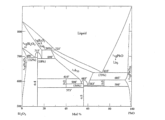
- FIG. 1 is a phase diagram of PbO—Bi 2 O 3 .
- FIG. 2 is a phase diagram of PbO—PbF 2 .
- a solute of Ga 2 O 3 and solvents of PbO and Bi 2 O 3 are mixed and melted, and then ⁇ -Ga 2 O is added to the resulting melt.
- the ⁇ -Ga 2 O 3 / ⁇ -Ga 2 O 3 laminate is obtained by bringing the three substrates into direct contact and growing a ⁇ -Ga 2 O 3 single crystal on the ⁇ -Ga 2 O 3 substrate by a liquid phase epitaxial growth method.
- a method for producing a ⁇ -Ga 2 O 3 / ⁇ -Ga 2 O 3 laminate characterized by obtaining The principle of the first embodiment of the present invention will be described below.
- PbO and Bi 2 O 3 form a eutectic system, and the melting point can be lowered by mixing the two.
- the melting point of the PbO+Bi 2 O 3 mixture can be made lower than the melting point of PbO alone or Bi 2 O 3 alone. This indicates that the evaporation amount of PbO or Bi 2 O 3 in the above PbO concentration range can be suppressed as compared with PbO or Bi 2 O 3 alone.
- PbO or Bi 2 O 3 When PbO or Bi 2 O 3 is used alone, the LPE growth temperature (the temperature during epitaxial growth) becomes high, so the mixed solvent as described above is suitable.
- the solute concentration is 14 mol % or more and 27 mol % or less. If the solute concentration is less than 5 mol %, the crystal growth rate will be slow, and if it exceeds 30 mol %, the LPE growth temperature will increase and solvent volatilization may increase. Also, the crystal growth speed increases, and the crystal quality may deteriorate.
- the growth rate of the layer containing the ⁇ -Ga 2 O 3 single crystal (epitaxial layer) formed by the liquid phase epitaxial growth method is preferably 10 to 50 ⁇ m/hr. More preferably ⁇ 30 ⁇ m/hr. If it is less than 10 ⁇ m/hr, the growth rate becomes slow and the cost may increase. Moreover, if it exceeds 50 ⁇ m/hr, the crystal quality may deteriorate.
- the growth rate can be obtained from the film thickness difference before and after the LPE growth and the growth time.
- the solute Ga 2 O 3 and the solvents PbO and PbF 2 are mixed and melted, and then ⁇ -Ga 2 is added to the resulting melt.
- a ⁇ -Ga 2 O 3 / ⁇ - Ga 2 O 3 stack is formed by directly contacting an O 3 substrate and growing a ⁇ - Ga 2 O 3 single crystal on the ⁇ -Ga 2 O 3 substrate by a liquid phase epitaxial growth method.
- Figure 2 is a phase diagram of PbO- PbF2 (Reference: C.
- PbO and PbF2 form a eutectic system, and the melting point can be lowered by mixing the two.
- the melting point of the PbO+PbF 2 mixture can be made lower than the melting point of PbO alone or PbF 2 alone. This indicates that the evaporation amount of PbO or PbF2 in the concentration range of PbO+ PbF2 can be suppressed as compared with PbO or PbF2 alone.
- the growth rate of the layer containing the ⁇ -Ga 2 O 3 single crystal (epitaxial layer) formed by the liquid phase epitaxial growth method is preferably 10 to 50 ⁇ m/hr. More preferably ⁇ 30 ⁇ m/hr. If it is less than 10 ⁇ m/hr, the growth rate becomes slow and the cost may increase. Moreover, if it exceeds 50 ⁇ m/hr, the crystal quality may deteriorate.
- the growth rate can be obtained from the film thickness difference before and after the LPE growth and the growth time.
- the LPE growth temperature is controlled, the solvent viscosity is adjusted, and the dissimilar element
- one or two or more third components can be added to the solvent. Examples include B 2 O 3 , V 2 O 5 , P 2 O 5 , MoO 3 and WO 3 .
- Bi 2 O 3 may be added as a third component to the solvent of the second embodiment. Liquid phase epitaxial growth using a ⁇ -Ga 2 O 3 substrate is most preferable as the method for growing the ⁇ -Ga 2 O 3 laminate in the present invention.
- Ga in ⁇ -Ga 2 O 3 is a trivalent oxide and generally exhibits n-type conductivity.
- ⁇ -Ga 2 O 3 is a trivalent oxide and generally exhibits n-type conductivity.
- by doping ⁇ -Ga 2 O 3 with a different element residual electron concentration, bandgap, insulating properties, etc. can be imparted.
- MgO or ZnO as a divalent impurity
- residual electrons can be reduced.
- SiO 2 or SnO 2 as a tetravalent impurity the residual electron concentration can be increased.
- Insulation can be imparted by doping Fe 2 O 3 .
- ⁇ -Ga 2 O 3 is doped with MgO or Al 2 O 3 which has a wider band gap than ⁇ -Ga 2 O 3 and mixed crystals are formed, the band gap can be increased. Also, by doping ZnO or CdO to form a mixed crystal, the bandgap can be reduced.
- the layer containing the ⁇ -Ga 2 O 3 single crystal formed by the liquid phase epitaxial growth method contains Be, Mg, Ca, Sr, Ba, Ti, Zr, Hf, Fe, Co, Ni, Cu, and Zn as heteroelements. , Cd, Al, In, Si, Ge, Sn and Pb, preferably in the range of 0.01 to 20 mol%, preferably in the range of 0.1 to 10 mol%. is more preferred. If the doping amount of the foreign element is less than 0.01 mol %, the characteristic expression may be poor, and if it exceeds 20 mol %, crystal growth may become difficult.
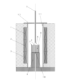
- FIG. 3 is a schematic diagram showing an example of a general LPE growth furnace.
- a platinum crucible 7 in which raw materials are melted and stored as a melt 8 is placed on a crucible base 9 made of mullite (compound of aluminum oxide and silicon dioxide).
- Three-stage side heaters (upper heater 1, central heater 2, lower heater 3) for heating and melting the raw material in the platinum crucible 7 are provided outside and laterally of the platinum crucible 7. .
- the outputs of the heaters are independently controlled, and the amount of heat applied to the melt 8 is adjusted independently.
- a mullite furnace core tube 11 is provided between the heater and the inner wall of the manufacturing furnace, and a mullite furnace cover 12 is provided above the furnace core tube 11 .
- a lifting mechanism is provided above the platinum crucible 7 .
- a lifting shaft 5 made of alumina is fixed to the lifting mechanism, and a substrate holder 6 and a substrate 4 fixed by the holder are provided at the tip of the shaft.
- a mechanism for rotating the shaft is provided on the upper portion of the pulling shaft 5 .
- a thermocouple 10 is provided at the bottom of the crucible.
- a third embodiment of the present invention is a ⁇ -Ga 2 O 3 / ⁇ -Ga 2 O 3 laminate having a layer containing a ⁇ -Ga 2 O 3 single crystal on a ⁇ -Ga 2 O 3 substrate, and the ⁇ -Ga 2 O 3 / ⁇ -Ga 2 O 3 laminate, wherein the rocking curve half width of the layer containing the ⁇ -Ga 2 O 3 single crystal is 5 to 100 arcsec.
- the ⁇ -Ga 2 O 3 / ⁇ -Ga 2 O 3 laminate of the present invention can be preferably produced by the first and second embodiments of the present invention described above.
- the rocking curve half width of the layer containing the ⁇ -Ga 2 O 3 single crystal is 5 to 100 arcsec, preferably 5 to 80 arcsec, more preferably 5 to 50 arcsec. If it exceeds 100 arcsec, the crystallinity is low, and the power device performance may deteriorate.
- the ⁇ -Ga 2 O 3 / ⁇ -Ga 2 O 3 laminate of the present invention is characterized by high crystallinity.
- the method described in Examples to be described later can be adopted as a method for measuring the rocking curve half-value width.
- a ⁇ -Ga 2 O 3 epitaxial layer is formed on a ⁇ -Ga 2 O 3 substrate. how to do this.
- the present invention is by no means limited to the following examples.
- a platinum crucible 7 in which raw materials are melted and stored as a melt 8 is placed on a crucible base 9 .
- Three-stage side heaters (upper heater 1, central heater 2, lower heater 3) for heating and melting the raw material in the platinum crucible 7 are provided outside and laterally of the platinum crucible 7. .
- the outputs of the heaters are independently controlled, and the amount of heat applied to the melt 8 is adjusted independently.
- a furnace core tube 11 is provided between the heater and the inner wall of the manufacturing furnace, and a furnace lid 12 is provided above the furnace core tube 11 .
- a lifting mechanism is provided above the platinum crucible 7 .
- a lifting shaft 5 made of alumina is fixed to the lifting mechanism, and a substrate holder 6 and a substrate 4 ( ⁇ -Ga 2 O 3 substrate) fixed by the holder are provided at the tip of the shaft.
- a mechanism for rotating the shaft is provided on the upper portion of the pulling shaft 5 .
- a thermocouple 10 is provided at the bottom of the crucible.
- the temperature of the manufacturing furnace is increased until the raw material melts.
- the temperature is preferably raised to 600 to 1000° C., more preferably 700 to 900° C., and allowed to stand still for 2 to 3 hours to homogenize the raw material melt.
- a plate made of platinum may be fixed to the tip of the alumina shaft, dipped in the melt, and the shaft rotated to stir to homogenize the melt. It is desirable that the growth of the ⁇ -Ga 2 O 3 single crystal layer proceeds only directly under the substrate.
- the three-stage heater is offset so that the bottom of the crucible is several degrees higher than the surface of the melt.
- the seed crystal substrate is brought into contact with the surface of the melt.
- the temperature is kept constant or the temperature is lowered at 0.025 to 5° C./hr to form the desired ⁇ -Ga 2 O 3 single crystal layer on the surface of the seed crystal substrate. grow.
- the seed crystal substrate is rotated at 5 to 300 rpm by the rotation of the growth shaft, and is reversely rotated at regular time intervals.
- the growing shaft is pulled up to separate the grown crystal from the melt, and the growing shaft is rotated at 50 to 300 rpm to separate the melt components adhering to the surface of the grown crystal. . Thereafter, it is cooled to room temperature over 1 to 24 hours to obtain the desired ⁇ -Ga 2 O 3 / ⁇ -Ga 2 O 3 laminate.
- Example 1 2661.2 g of PbO (99.999% purity), 2777.7 g of Bi 2 O 3 (99.999% purity) and Ga 2 O 3 are placed in a platinum crucible 7 having an inner diameter of 120 mm, a height of 150 mm and a thickness of 1 mm. (99.999% purity) was charged in an amount of 561.2 g.
- the platinum crucible 7 charged with raw materials was placed in the LPE furnace shown in FIG. After stirring the melt for 6 hours using a platinum plate, the temperature was lowered until the bottom temperature of the crucible reached 750° C., and ⁇ -Ga 2 O 3 with a C-plane orientation of 11 mm ⁇ 11 mm ⁇ thickness of 650 ⁇ m grown by the EFG method. The substrate was wetted. The growth was carried out at the same temperature for 3 hours while rotating the pulling shaft 5 made of alumina at 60 rpm. At this time, the shaft rotation was reversed every 5 minutes. After that, the pull-up shaft 5 was pulled up to separate from the melt, and the melt components were separated by rotating the pull-up shaft 5 at 200 rpm.
- a ⁇ -Ga 2 O 3 / ⁇ -Ga 2 O 3 laminate was obtained.
- the melt components that could not be completely removed were removed using hydrochloric acid.
- the average thickness of the epitaxial layer was about 90 ⁇ m.
- the average growth rate was about 30 ⁇ m/hr.
- the rocking curve half width was measured using an X-ray diffractometer (X'pert MRD manufactured by Spectris). Using the same apparatus, after adjusting 2 ⁇ , ⁇ , ⁇ and ⁇ and setting the axis so that the peak of the (002) plane of ⁇ -Ga 2 O 3 can be detected, measurement was performed at a tube voltage of 45 KV and a tube current of 40 mA. . The incident light was made monochromatic by using four crystals of Ge (220) plane. Other measurement conditions were as follows.
- ⁇ scan incidence angle scan
- ⁇ range set the angle at which the ⁇ -Ga 2 O 3 (002) plane appears for each sample
- ⁇ range 0.1 deg ⁇ step
- 0.0005deg 2 ⁇ position set the angle at which the ⁇ -Ga 2 O 3 (002) plane appears for each sample
- Collimator diameter 0.5 mm Anti-scattering slit; 1.5mm
- Example 2 ⁇ -Ga 2 O 3 / was prepared in the same manner as in Example 1 except that the charging composition was changed so as to have the composition shown in Table 1 below, and the raw material melting temperature and growth temperature were changed as shown in Table 1.
- a ⁇ -Ga 2 O 3 laminate was obtained.
- the epitaxial layer obtained in Example 2 is a mixed crystal layer of ⁇ -Ga 2 O 3 and MgO
- the epitaxial layer obtained in Example 5 is a mixed crystal layer of ⁇ -Ga 2 O 3 and Al 2 O 3 . It was a mixed crystal layer of
- the solute Ga 2 O 3 and the solvents PbO and Bi 2 O 3 are mixed and dissolved, and then the ⁇ -Ga 2 O 3 substrate is brought into direct contact with the resulting melt.
- a ⁇ -Ga 2 O 3 / ⁇ -Ga 2 O 3 laminate can be produced.
- the melting point of the solvent can be made lower than that of PbO or Bi 2 O 3 alone. Therefore, both the raw material dissolution temperature and the ⁇ -Ga 2 O 3 growth temperature are lower than when a single solvent is used. This means that the amount of evaporation of solvent components can be reduced.
- the present invention provides a liquid phase growth method close to thermal equilibrium growth. Therefore, as shown in Table 1 above, the growth rate is as high as 13 to 30 ⁇ m/hr, the rocking curve half width is as narrow as 15 to 28 arcsec, and the crystallinity is high. On the other hand, Comparative Examples 1 and 2 were not melted unless heat exceeding 1000° C. was applied, and the solvent was volatilized at a temperature exceeding 1000° C., so a laminate could not be produced.
- the platinum crucible 7 charged with raw materials was placed in the LPE furnace shown in FIG. After stirring the melt for 6 hours using a platinum plate, the temperature was lowered until the bottom temperature of the crucible reached 840° C., and a ⁇ -Ga 2 O 3 with a C-plane orientation of 11 mm ⁇ 11 mm ⁇ thickness of 650 ⁇ m grown by the EFG method. The substrate was wetted. The growth was carried out at the same temperature for 3 hours while rotating the pulling shaft 5 made of alumina at 60 rpm. At this time, the shaft rotation was reversed every 5 minutes. After that, the pull-up shaft 5 was pulled up to separate from the melt, and the melt components were separated by rotating the pull-up shaft 5 at 200 rpm.
- a ⁇ -Ga 2 O 3 / ⁇ -Ga 2 O 3 laminate was obtained.
- the melt components that could not be completely removed were removed using nitric acid.
- the average thickness of the epitaxial layer was about 69 ⁇ m.
- the average growth rate was about 23 ⁇ m/hr.
- Examples 10-11, Comparative Example 3 ⁇ -Ga 2 O 3 / ⁇ was prepared in the same manner as in Example 9 except that the charging composition was changed so as to have the composition shown in Table 2 below, and the raw material melting temperature and growth temperature were changed as shown in Table 2. - Ga 2 O 3 laminate was obtained.
- Example 12-13 ⁇ -Ga 2 O 3 / ⁇ was prepared in the same manner as in Example 9 except that the charging composition was changed so as to have the composition shown in Table 3 below, and the raw material melting temperature and growth temperature were changed as shown in Table 3. - Ga 2 O 3 laminate was obtained. If the concentration of Ga 2 O 3 as a solute is less than 2 mol %, it approaches the melting point of the solvent, and the solvent tends to be viscous, making stable crystal growth difficult. Also, when the solute concentration exceeds 20 mol %, the growth temperature may become high. Therefore, the concentration of the solute Ga 2 O 3 is preferably 2 to 20 mol %.
- the solute Ga 2 O 3 and the solvents PbO and PbF 2 are mixed and dissolved, and then the ⁇ -Ga 2 O 3 substrate is brought into direct contact with the obtained melt. , ⁇ -Ga 2 O 3 / ⁇ -Ga 2 O 3 laminates can be produced.
- ⁇ -Ga 2 O 3 / ⁇ -Ga 2 O 3 laminates can be produced.
- the melting point of the solvent can be made lower than that of PbO or PbF 2 alone. Therefore, both the raw material dissolution temperature and the ⁇ -Ga 2 O 3 growth temperature are lower than when a single solvent is used. This means that the amount of evaporation of solvent components can be reduced.
- the present invention provides a liquid phase growth method close to thermal equilibrium growth. Therefore, as shown in Tables 2 and 3 above, the growth rate is as high as 18 to 29 ⁇ m/hr, the rocking curve half width is as narrow as 35 to 77 arcsec, and the crystallinity is high. On the other hand, in Comparative Example 3, the laminate was not melted unless heat exceeding 1000° C. was applied, and the solvent volatilized at a temperature exceeding 1000° C., so that a laminate could not be produced.
Landscapes
- Chemical & Material Sciences (AREA)
- Engineering & Computer Science (AREA)
- Crystallography & Structural Chemistry (AREA)
- Materials Engineering (AREA)
- Metallurgy (AREA)
- Organic Chemistry (AREA)
- Inorganic Chemistry (AREA)
- Crystals, And After-Treatments Of Crystals (AREA)
- Liquid Deposition Of Substances Of Which Semiconductor Devices Are Composed (AREA)
- Recrystallisation Techniques (AREA)
Priority Applications (6)
| Application Number | Priority Date | Filing Date | Title |
|---|---|---|---|
| EP22887161.2A EP4411028B1 (en) | 2021-11-01 | 2022-10-28 | Method for producing beta-ga2o3/beta-ga2o3 multilayer body |
| US18/703,762 US20240417881A1 (en) | 2021-11-01 | 2022-10-28 | Method for producing beta-ga2o3/beta-ga2o3 multilayer body |
| JP2023512692A JP7380948B2 (ja) | 2021-11-01 | 2022-10-28 | β-Ga2O3/β-Ga2O3積層体の製造方法 |
| CN202280071198.5A CN118159694A (zh) | 2021-11-01 | 2022-10-28 | β-Ga₂O₃/β-Ga₂O₃层叠体的制造方法 |
| KR1020247008343A KR102927254B1 (ko) | 2021-11-01 | 2022-10-28 | β-Ga2O3/β-Ga2O3 적층체의 제조 방법 |
| JP2023110746A JP2023134567A (ja) | 2021-11-01 | 2023-07-05 | β-Ga2O3/β-Ga2O3積層体の製造方法 |
Applications Claiming Priority (2)
| Application Number | Priority Date | Filing Date | Title |
|---|---|---|---|
| JP2021178650 | 2021-11-01 | ||
| JP2021-178650 | 2021-11-01 |
Publications (1)
| Publication Number | Publication Date |
|---|---|
| WO2023074836A1 true WO2023074836A1 (ja) | 2023-05-04 |
Family
ID=86159992
Family Applications (1)
| Application Number | Title | Priority Date | Filing Date |
|---|---|---|---|
| PCT/JP2022/040309 Ceased WO2023074836A1 (ja) | 2021-11-01 | 2022-10-28 | β-Ga2O3/β-Ga2O3積層体の製造方法 |
Country Status (7)
| Country | Link |
|---|---|
| US (1) | US20240417881A1 (https=) |
| EP (1) | EP4411028B1 (https=) |
| JP (2) | JP7380948B2 (https=) |
| KR (1) | KR102927254B1 (https=) |
| CN (1) | CN118159694A (https=) |
| TW (1) | TW202328516A (https=) |
| WO (1) | WO2023074836A1 (https=) |
Cited By (1)
| Publication number | Priority date | Publication date | Assignee | Title |
|---|---|---|---|---|
| CN119041012A (zh) * | 2024-10-30 | 2024-11-29 | 安徽科瑞思创晶体材料有限责任公司 | 一种利用液相外延制备稀土掺杂钇铁石榴石薄膜的方法 |
Families Citing this family (1)
| Publication number | Priority date | Publication date | Assignee | Title |
|---|---|---|---|---|
| TW202600920A (zh) * | 2024-02-22 | 2026-01-01 | 日商三菱瓦斯化學股份有限公司 | β-Ga2O3/β-Ga2O3疊層體之製造方法、利用該製造方法而得到的疊層體、及含有該疊層體之半導體裝置 |
Citations (4)
| Publication number | Priority date | Publication date | Assignee | Title |
|---|---|---|---|---|
| JP2010280533A (ja) * | 2009-06-04 | 2010-12-16 | Mitsubishi Gas Chemical Co Inc | 液相エピタキシャル成長法による励起子発光型ZnOシンチレータの製造方法 |
| JP5794955B2 (ja) | 2012-07-11 | 2015-10-14 | 信越化学工業株式会社 | β−Ga2O3単結晶膜付基板の製造方法 |
| JP2019182744A (ja) * | 2019-07-31 | 2019-10-24 | 株式会社タムラ製作所 | Ga2O3系単結晶基板 |
| JP6744523B2 (ja) | 2015-12-16 | 2020-08-19 | 株式会社タムラ製作所 | 半導体基板、並びにエピタキシャルウエハ及びその製造方法 |
Family Cites Families (3)
| Publication number | Priority date | Publication date | Assignee | Title |
|---|---|---|---|---|
| JP3679097B2 (ja) * | 2002-05-31 | 2005-08-03 | 株式会社光波 | 発光素子 |
| CN102251281B (zh) * | 2006-03-01 | 2013-01-16 | 三菱瓦斯化学株式会社 | 采用液相生长法的ZnO单晶的制造方法 |
| JP5747110B1 (ja) * | 2014-06-30 | 2015-07-08 | 株式会社タムラ製作所 | Ga2O3系単結晶基板 |
-
2022
- 2022-10-28 EP EP22887161.2A patent/EP4411028B1/en active Active
- 2022-10-28 KR KR1020247008343A patent/KR102927254B1/ko active Active
- 2022-10-28 CN CN202280071198.5A patent/CN118159694A/zh active Pending
- 2022-10-28 US US18/703,762 patent/US20240417881A1/en active Pending
- 2022-10-28 WO PCT/JP2022/040309 patent/WO2023074836A1/ja not_active Ceased
- 2022-10-28 JP JP2023512692A patent/JP7380948B2/ja active Active
- 2022-10-31 TW TW111141303A patent/TW202328516A/zh unknown
-
2023
- 2023-07-05 JP JP2023110746A patent/JP2023134567A/ja active Pending
Patent Citations (4)
| Publication number | Priority date | Publication date | Assignee | Title |
|---|---|---|---|---|
| JP2010280533A (ja) * | 2009-06-04 | 2010-12-16 | Mitsubishi Gas Chemical Co Inc | 液相エピタキシャル成長法による励起子発光型ZnOシンチレータの製造方法 |
| JP5794955B2 (ja) | 2012-07-11 | 2015-10-14 | 信越化学工業株式会社 | β−Ga2O3単結晶膜付基板の製造方法 |
| JP6744523B2 (ja) | 2015-12-16 | 2020-08-19 | 株式会社タムラ製作所 | 半導体基板、並びにエピタキシャルウエハ及びその製造方法 |
| JP2019182744A (ja) * | 2019-07-31 | 2019-10-24 | 株式会社タムラ製作所 | Ga2O3系単結晶基板 |
Non-Patent Citations (5)
| Title |
|---|
| C. SANDONNINI ATTI: "Accad. Naz. Licei", SCI. FIS. MAT. NAT., vol. 23, 1914, pages 962 - 964 |
| J. AM. CHEM. SOC., vol. 64, no. 3, 1981, pages 182 - 184 |
| JOURNAL OF THE JAPANESE ASSOCIATION FOR CRYSTAL GROWTH, vol. 42, no. 2, 2015, pages 141 - 147 |
| See also references of EP4411028A4 |
| YOKOYAMA, MITSUNORI: "Study of Crystal Growth Methods for Zirconia-, Hafnia-, and Titania-Based Oxides", PH.D. THESIS, HOKKAIDO UNIVERSITY, 25 March 1993 (1993-03-25), pages 8 - 14, XP009545267, DOI: 10.11501/3093008 * |
Cited By (1)
| Publication number | Priority date | Publication date | Assignee | Title |
|---|---|---|---|---|
| CN119041012A (zh) * | 2024-10-30 | 2024-11-29 | 安徽科瑞思创晶体材料有限责任公司 | 一种利用液相外延制备稀土掺杂钇铁石榴石薄膜的方法 |
Also Published As
| Publication number | Publication date |
|---|---|
| EP4411028A4 (en) | 2024-12-04 |
| CN118159694A (zh) | 2024-06-07 |
| KR20240045295A (ko) | 2024-04-05 |
| EP4411028C0 (en) | 2026-02-25 |
| EP4411028A1 (en) | 2024-08-07 |
| JPWO2023074836A1 (https=) | 2023-05-04 |
| JP2023134567A (ja) | 2023-09-27 |
| KR102927254B1 (ko) | 2026-02-12 |
| EP4411028B1 (en) | 2026-02-25 |
| US20240417881A1 (en) | 2024-12-19 |
| JP7380948B2 (ja) | 2023-11-15 |
| TW202328516A (zh) | 2023-07-16 |
Similar Documents
| Publication | Publication Date | Title |
|---|---|---|
| CN102251281B (zh) | 采用液相生长法的ZnO单晶的制造方法 | |
| Dang et al. | Recent progress in the synthesis of hybrid halide perovskite single crystals | |
| CN103781947B (zh) | 晶体层叠结构体 | |
| JP5304793B2 (ja) | 炭化珪素単結晶の製造方法 | |
| JP7380948B2 (ja) | β-Ga2O3/β-Ga2O3積層体の製造方法 | |
| JP5260881B2 (ja) | Mg含有ZnO系混晶単結晶、その積層体およびそれらの製造方法 | |
| WO2014103394A1 (ja) | n型SiC単結晶の製造方法 | |
| CN117822122B (zh) | 一种层状Ge1-xSb4+xTe7单晶体及其制备方法 | |
| EP4703501A1 (en) | Method for producing ?-ga2o3/?-ga2o3 layered product, and layered product obtained using said production method | |
| WO2009119411A1 (ja) | ZnO単結晶の製造方法、それによって得られた自立ZnO単結晶ウエファー、並びに自立Mg含有ZnO系混晶単結晶ウエファーおよびそれに用いるMg含有ZnO系混晶単結晶の製造方法 | |
| JP2004203721A (ja) | 単結晶成長装置および成長方法 | |
| TW202432918A (zh) | 熔融生長塊狀β-(AlxGa-x)O單晶及用於製造塊狀β-(AlxGa-x)O單晶的方法 | |
| JP3548910B2 (ja) | ZnO単結晶の製造方法 | |
| TW202600920A (zh) | β-Ga2O3/β-Ga2O3疊層體之製造方法、利用該製造方法而得到的疊層體、及含有該疊層體之半導體裝置 | |
| JP3906359B2 (ja) | P形半導体SrCu2O2単結晶の製造方法 | |
| JP2018080063A (ja) | SiC単結晶の製造方法 | |
| JP2000154096A (ja) | SiC結晶の液相エピタキシャル成長方法 | |
| UA26253U (en) | METHOD FOR PRODUCING Cu2CdGeS4 MONOCRYSTALS |
Legal Events
| Date | Code | Title | Description |
|---|---|---|---|
| WWE | Wipo information: entry into national phase |
Ref document number: 2023512692 Country of ref document: JP |
|
| 121 | Ep: the epo has been informed by wipo that ep was designated in this application |
Ref document number: 22887161 Country of ref document: EP Kind code of ref document: A1 |
|
| WWE | Wipo information: entry into national phase |
Ref document number: 18703762 Country of ref document: US Ref document number: 202280071198.5 Country of ref document: CN |
|
| ENP | Entry into the national phase |
Ref document number: 2022887161 Country of ref document: EP Effective date: 20240502 |
|
| WWR | Wipo information: refused in national office |
Ref document number: 1020247008343 Country of ref document: KR |
|
| WWC | Wipo information: continuation of processing after refusal or withdrawal |
Ref document number: 1020247008343 Country of ref document: KR |
|
| WWG | Wipo information: grant in national office |
Ref document number: 2022887161 Country of ref document: EP |